High Power Infrared Emitting Diode, 850 nm, Surface ... · • Dimensions (L x W x H in mm): 3.85 x...
7
VSMY9857535 www.vishay.com Vishay Semiconductors Rev. 1.0, 05-Jul-16 1 Document Number: 84359 For technical questions, contact: [email protected] THIS DOCUMENT IS SUBJECT TO CHANGE WITHOUT NOTICE. THE PRODUCTS DESCRIBED HEREIN AND THIS DOCUMENT ARE SUBJECT TO SPECIFIC DISCLAIMERS, SET FORTH AT www.vishay.com/doc?91000 High Power Infrared Emitting Diode, 850 nm, Surface Emitter Technology DESCRIPTION As part of the SurfLight TM portfolio, the VSMY9857535 is an infrared, 850 nm emitting diode based on surface emitter technology with high radiant power and high speed, molded in low thermal resistance SMD package with lens. A 35 mil chip provides outstanding radiant intensity and allows DC operation of the device up to 1.0 A. FEATURES • Package type: surface mount • Package form: high power SMD with lens • Dimensions (L x W x H in mm): 3.85 x 3.85 x 1.51 • Peak wavelength: λ p = 850 nm • High radiant power • High radiant intensity • Angle of half intensity: ϕ = ± 75° • Designed for high drive currents: up to 1.0 A (DC) and up to 5 A pulses • Low thermal resistance: R thJP = 10 K/W • Floor life: 168 h, MSL 3, according to J-STD-020 • Lead (Pb)-free reflow soldering • Material categorization: for definitions of compliance please see www.vishay.com/doc?99912 APPLICATIONS • Infrared illumination for CMOS cameras (CCTV, 3D gaming) • Machine vision • Bio identification Note • Test conditions see table “Basic Characteristics” Note • MOQ: minimum order quantity PRODUCT SUMMARY COMPONENT I e (mW/sr) ϕ (deg) λ p (nm) t r (ns) VSMY9857535 180 ± 75 850 30 ORDERING INFORMATION ORDERING CODE PACKAGING REMARKS PACKAGE FORM VSMY9857535 Tape and reel MOQ: 600 pcs, 600 pcs/reel High power with lens ABSOLUTE MAXIMUM RATINGS (T amb = 25 °C, unless otherwise specified) PARAMETER TEST CONDITION SYMBOL VALUE UNIT Reverse voltage V R 5 V Forward current I F 1 A Peak forward current t p /T = 0.5, t p = 100 μs I FM 2 A Surge forward current t p = 100 μs I FSM 5 A Power dissipation P V 2.5 W Junction temperature T j 115 °C Operating temperature range T amb -40 to +85 °C Storage temperature range T stg -55 to +100 °C Soldering temperature According to Fig. 10, J-STD-20 T sd 260 °C Thermal resistance junction / pin JESD 51 R thJP 10 K/W
-
Upload
truongliem -
Category
Documents
-
view
221 -
download
0
Transcript of High Power Infrared Emitting Diode, 850 nm, Surface ... · • Dimensions (L x W x H in mm): 3.85 x...
VSMY9857535www.vishay.com Vishay Semiconductors
Rev. 1.0, 05-Jul-16 1 Document Number: 84359For technical questions, contact: [email protected]
THIS DOCUMENT IS SUBJECT TO CHANGE WITHOUT NOTICE. THE PRODUCTS DESCRIBED HEREIN AND THIS DOCUMENTARE SUBJECT TO SPECIFIC DISCLAIMERS, SET FORTH AT www.vishay.com/doc?91000
High Power Infrared Emitting Diode, 850 nm,Surface Emitter Technology
DESCRIPTIONAs part of the SurfLightTM portfolio, the VSMY9857535 is an infrared, 850 nm emitting diode based on surface emitter technology with high radiant power and high speed, molded in low thermal resistance SMD package with lens. A 35 mil chip provides outstanding radiant intensity and allows DC operation of the device up to 1.0 A.
FEATURES• Package type: surface mount• Package form: high power SMD with lens• Dimensions (L x W x H in mm): 3.85 x 3.85 x 1.51• Peak wavelength: λp = 850 nm• High radiant power• High radiant intensity• Angle of half intensity: ϕ = ± 75°• Designed for high drive currents: up to 1.0 A (DC)
and up to 5 A pulses• Low thermal resistance: RthJP = 10 K/W• Floor life: 168 h, MSL 3, according to J-STD-020• Lead (Pb)-free reflow soldering• Material categorization: for definitions of compliance
please see www.vishay.com/doc?99912
APPLICATIONS• Infrared illumination for CMOS cameras (CCTV, 3D
gaming)• Machine vision• Bio identification
Note• Test conditions see table “Basic Characteristics”
Note• MOQ: minimum order quantity
PRODUCT SUMMARYCOMPONENT Ie (mW/sr) ϕ (deg) λp (nm) tr (ns)
VSMY9857535 180 ± 75 850 30
ORDERING INFORMATIONORDERING CODE PACKAGING REMARKS PACKAGE FORM
VSMY9857535 Tape and reel MOQ: 600 pcs, 600 pcs/reel High power with lens
ABSOLUTE MAXIMUM RATINGS (Tamb = 25 °C, unless otherwise specified)PARAMETER TEST CONDITION SYMBOL VALUE UNIT
Reverse voltage VR 5 V
Forward current IF 1 A
Peak forward current tp/T = 0.5, tp = 100 μs IFM 2 A
Surge forward current tp = 100 μs IFSM 5 A
Power dissipation PV 2.5 W
Junction temperature Tj 115 °C
Operating temperature range Tamb -40 to +85 °C
Storage temperature range Tstg -55 to +100 °C
Soldering temperature According to Fig. 10, J-STD-20 Tsd 260 °C
Thermal resistance junction / pin JESD 51 RthJP 10 K/W
VSMY9857535www.vishay.com Vishay Semiconductors
Rev. 1.0, 05-Jul-16 2 Document Number: 84359For technical questions, contact: [email protected]
THIS DOCUMENT IS SUBJECT TO CHANGE WITHOUT NOTICE. THE PRODUCTS DESCRIBED HEREIN AND THIS DOCUMENTARE SUBJECT TO SPECIFIC DISCLAIMERS, SET FORTH AT www.vishay.com/doc?91000
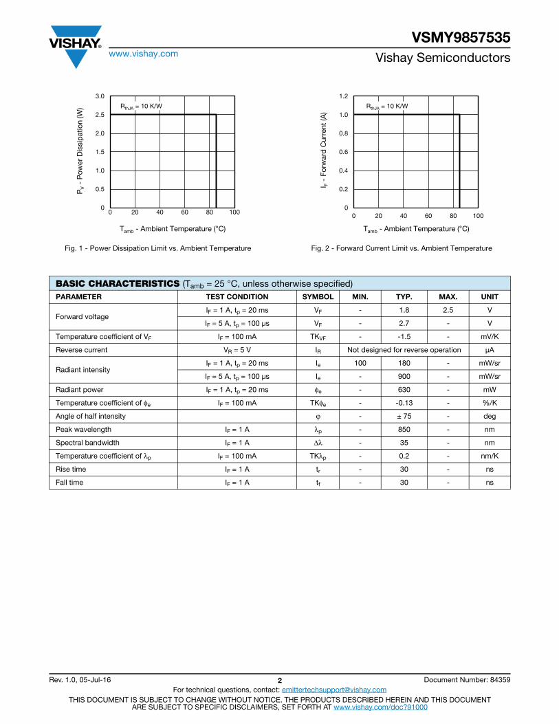
Fig. 1 - Power Dissipation Limit vs. Ambient Temperature Fig. 2 - Forward Current Limit vs. Ambient Temperature
0
0.5
1.0
1.5
2.0
2.5
3.0
0 20 40 60 80 100
PV
-P
ower
Dissi
pat
ion
(W)
Tamb - Ambient Temperature (°C)
RthJA = 10 K/W
0
0.2
0.4
0.6
0.8
1.0
1.2
0 20 40 60 80 100
I F-
Forw
ard
Cur
rent
(A)
Tamb - Ambient Temperature (°C)
RthJA = 10 K/W
BASIC CHARACTERISTICS (Tamb = 25 °C, unless otherwise specified)PARAMETER TEST CONDITION SYMBOL MIN. TYP. MAX. UNIT
Forward voltageIF = 1 A, tp = 20 ms VF - 1.8 2.5 V
IF = 5 A, tp = 100 μs VF - 2.7 - V
Temperature coefficient of VF IF = 100 mA TKVF - -1.5 - mV/K
Reverse current VR = 5 V IR Not designed for reverse operation μA
Radiant intensityIF = 1 A, tp = 20 ms Ie 100 180 - mW/sr
IF = 5 A, tp = 100 μs Ie - 900 - mW/sr
Radiant power IF = 1 A, tp = 20 ms φe - 630 - mW
Temperature coefficient of φe IF = 100 mA TKφe - -0.13 - %/K
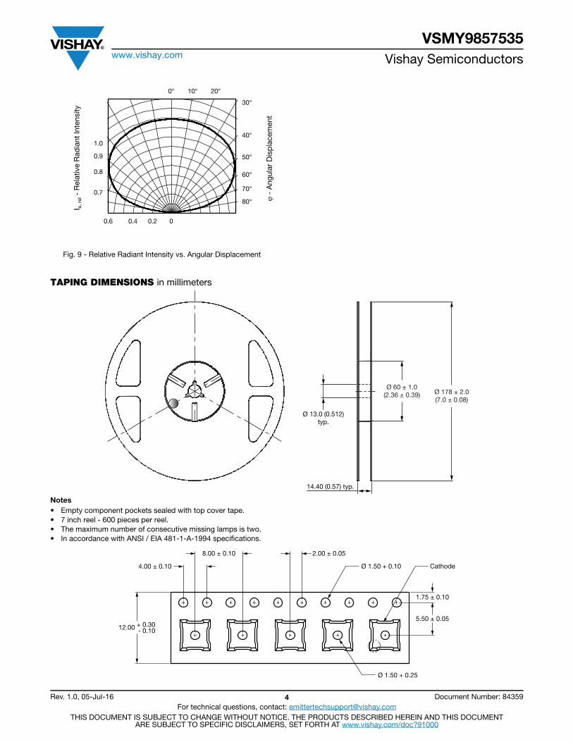
Angle of half intensity ϕ - ± 75 - deg
Peak wavelength IF = 1 A λp - 850 - nm
Spectral bandwidth IF = 1 A Δλ - 35 - nm
Temperature coefficient of λp IF = 100 mA TKλp - 0.2 - nm/K
Rise time IF = 1 A tr - 30 - ns
Fall time IF = 1 A tf - 30 - ns
VSMY9857535www.vishay.com Vishay Semiconductors
Rev. 1.0, 05-Jul-16 3 Document Number: 84359For technical questions, contact: [email protected]
THIS DOCUMENT IS SUBJECT TO CHANGE WITHOUT NOTICE. THE PRODUCTS DESCRIBED HEREIN AND THIS DOCUMENTARE SUBJECT TO SPECIFIC DISCLAIMERS, SET FORTH AT www.vishay.com/doc?91000
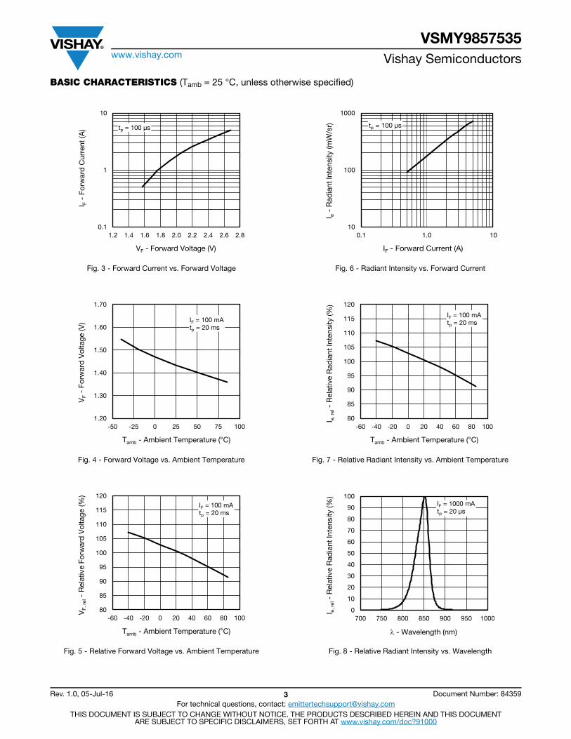
BASIC CHARACTERISTICS (Tamb = 25 °C, unless otherwise specified)
Fig. 3 - Forward Current vs. Forward Voltage
Fig. 4 - Forward Voltage vs. Ambient Temperature
Fig. 5 - Relative Forward Voltage vs. Ambient Temperature
Fig. 6 - Radiant Intensity vs. Forward Current
Fig. 7 - Relative Radiant Intensity vs. Ambient Temperature
Fig. 8 - Relative Radiant Intensity vs. Wavelength
0.1
1
10
1.2 1.4 1.6 1.8 2.0 2.2 2.4 2.6 2.8
I F-
Forw
ard
Cur
rent
(A)
VF - Forward Voltage (V)
tp = 100 μs
1.20
1.30
1.40
1.50
1.60
1.70
-50 -25 0 25 50 75 100
VF
-Fo
rwar
d V
olta
ge (V
)
Tamb - Ambient Temperature (°C)
IF = 100 mAtp = 20 ms
80
85
90
95
100
105
110
115
120
-60 -40 -20 0 20 40 60 80 100
VF,
rel
-R
elat
ive
Forw
ard
Vol
tage
(%)
Tamb - Ambient Temperature (°C)
IF = 100 mAtp = 20 ms
10
100
1000
0.1 1.0 10
I e-
Rad
iant
Inte
nsity
(mW
/sr)
IF - Forward Current (A)
tp = 100 μs
80
85
90
95
100
105
110
115
120
-60 -40 -20 0 20 40 60 80 100
I e, r
el-
Rel
ativ
e R
adia
nt In
tens
ity (%
)
Tamb - Ambient Temperature (°C)
IF = 100 mAtp = 20 ms
0
10
20
30
40
50
60
70
80
90
100
700 750 800 850 900 950 1000
I e, r
el-
Rel
ativ
e R
adia
nt In
tens
ity (%
)
λ - Wavelength (nm)
IF = 1000 mAtp = 20 μs
VSMY9857535www.vishay.com Vishay Semiconductors
Rev. 1.0, 05-Jul-16 4 Document Number: 84359For technical questions, contact: [email protected]
THIS DOCUMENT IS SUBJECT TO CHANGE WITHOUT NOTICE. THE PRODUCTS DESCRIBED HEREIN AND THIS DOCUMENTARE SUBJECT TO SPECIFIC DISCLAIMERS, SET FORTH AT www.vishay.com/doc?91000
Fig. 9 - Relative Radiant Intensity vs. Angular Displacement
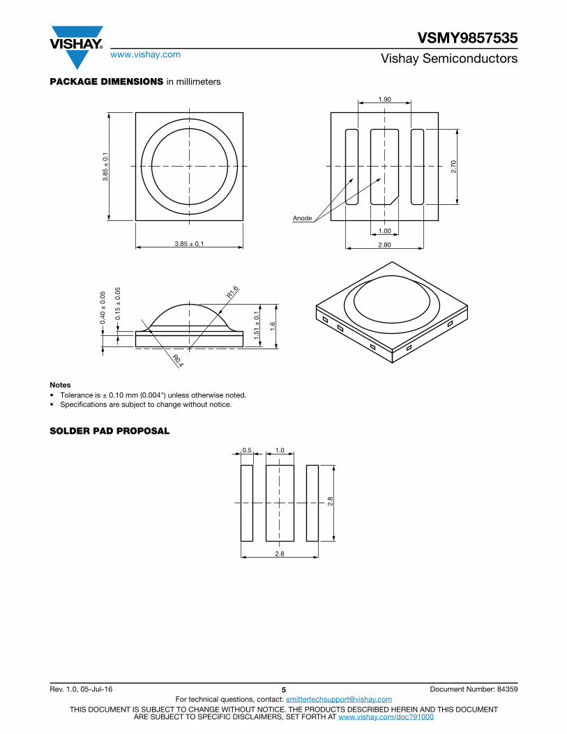
TAPING DIMENSIONS in millimeters
Notes• Empty component pockets sealed with top cover tape.• 7 inch reel - 600 pieces per reel.• The maximum number of consecutive missing lamps is two.• In accordance with ANSI / EIA 481-1-A-1994 specifications.
I e, r
el -
Rel
ativ
e R
adia
nt In
tens
ity
0.6
80°
0°
0.7
0.4 0.2 0
30°
70°
60°
50°
40°
10° 20°
1.0
0.9
0.8
ϕ -
Ang
ular
Dis
pla
cem
ent
Ø 178 ± 2.0(7.0 ± 0.08)
Ø 60 ± 1.0(2.36 ± 0.39)
Ø 13.0 (0.512)typ.
14.40 (0.57) typ.
4.00 ± 0.10
8.00 ± 0.10
12.00 + 0.30- 0.10
2.00 ± 0.05
1.75 ± 0.10
5.50 ± 0.05
Ø 1.50 + 0.10
Ø 1.50 + 0.25
Cathode
VSMY9857535www.vishay.com Vishay Semiconductors
Rev. 1.0, 05-Jul-16 5 Document Number: 84359For technical questions, contact: [email protected]
THIS DOCUMENT IS SUBJECT TO CHANGE WITHOUT NOTICE. THE PRODUCTS DESCRIBED HEREIN AND THIS DOCUMENTARE SUBJECT TO SPECIFIC DISCLAIMERS, SET FORTH AT www.vishay.com/doc?91000
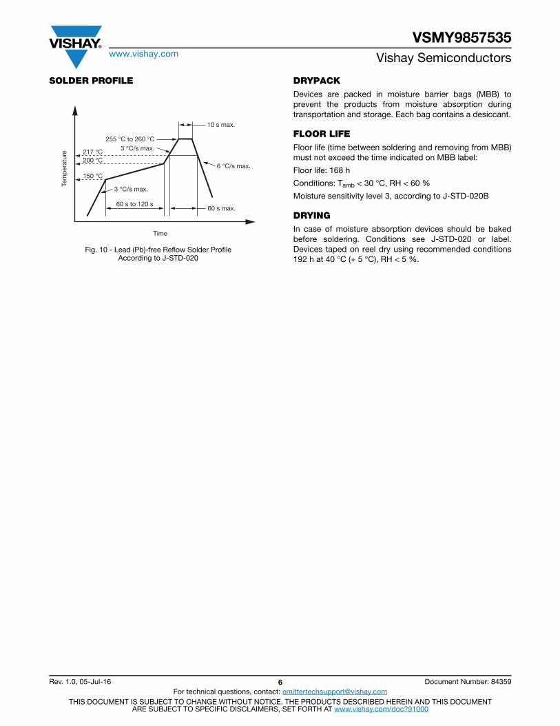
PACKAGE DIMENSIONS in millimeters
Notes• Tolerance is ± 0.10 mm (0.004") unless otherwise noted.• Specifications are subject to change without notice.
SOLDER PAD PROPOSAL
3.85
± 0
.1
3.85 ± 0.1
1.00
2.80
2.70
1.90
Anode
1.6
1.51
± 0
.1
R1.6
R0.4
0.40
± 0
.05
0.15
± 0
.05
2.8
2.8
0.5 1.0
VSMY9857535www.vishay.com Vishay Semiconductors
Rev. 1.0, 05-Jul-16 6 Document Number: 84359For technical questions, contact: [email protected]
THIS DOCUMENT IS SUBJECT TO CHANGE WITHOUT NOTICE. THE PRODUCTS DESCRIBED HEREIN AND THIS DOCUMENTARE SUBJECT TO SPECIFIC DISCLAIMERS, SET FORTH AT www.vishay.com/doc?91000
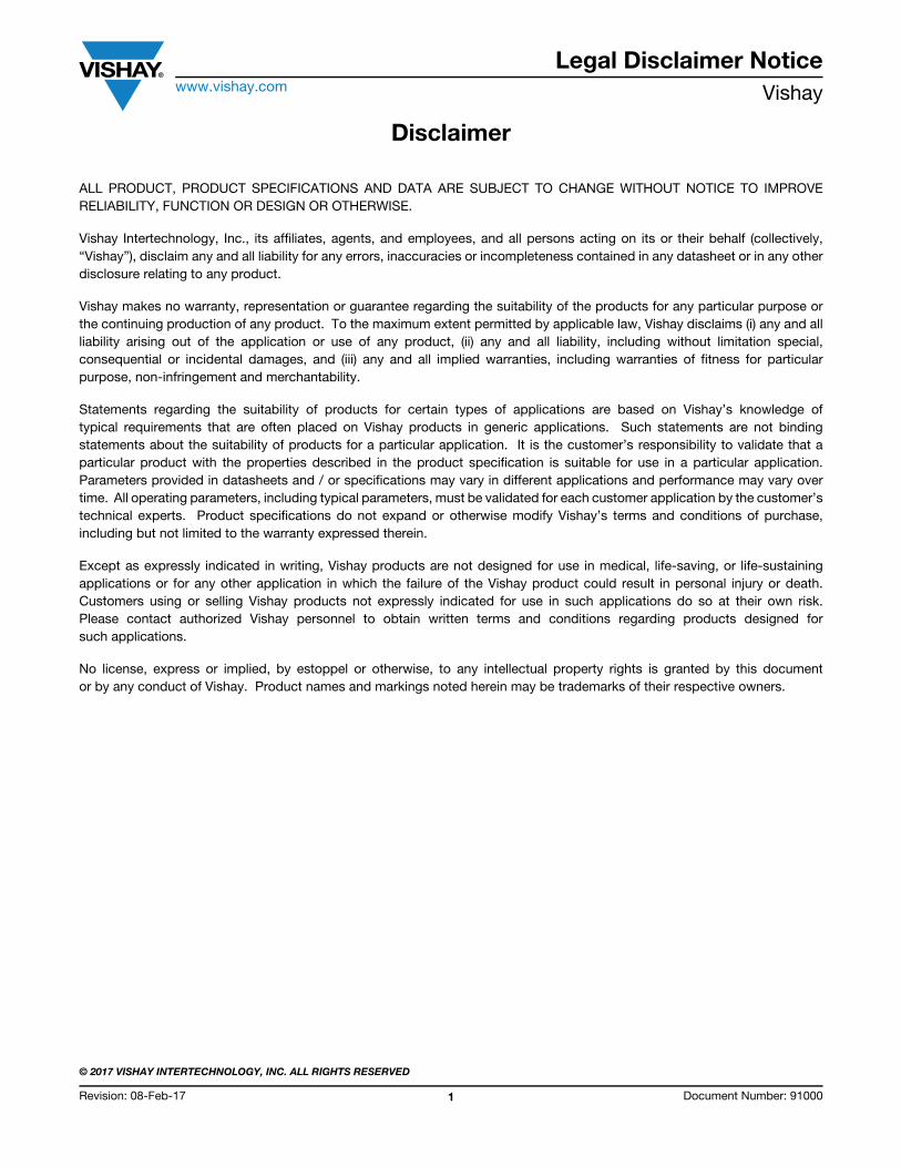
SOLDER PROFILE
Fig. 10 - Lead (Pb)-free Reflow Solder ProfileAccording to J-STD-020
DRYPACKDevices are packed in moisture barrier bags (MBB) to prevent the products from moisture absorption during transportation and storage. Each bag contains a desiccant.
FLOOR LIFEFloor life (time between soldering and removing from MBB) must not exceed the time indicated on MBB label:
Floor life: 168 h
Conditions: Tamb < 30 °C, RH < 60 %
Moisture sensitivity level 3, according to J-STD-020B
DRYINGIn case of moisture absorption devices should be baked before soldering. Conditions see J-STD-020 or label. Devices taped on reel dry using recommended conditions 192 h at 40 °C (+ 5 °C), RH < 5 %.
255 °C to 260 °C
10 s max.
6 °C/s max.
3 °C/s max.
3 °C/s max.
150 °C
200 °C217 °C
60 s to 120 s60 s max.
Time
Tem
per
atur
e
Legal Disclaimer Noticewww.vishay.com Vishay
Revision: 08-Feb-17 1 Document Number: 91000
DisclaimerALL PRODUCT, PRODUCT SPECIFICATIONS AND DATA ARE SUBJECT TO CHANGE WITHOUT NOTICE TO IMPROVE RELIABILITY, FUNCTION OR DESIGN OR OTHERWISE.
Vishay Intertechnology, Inc., its affiliates, agents, and employees, and all persons acting on its or their behalf (collectively, “Vishay”), disclaim any and all liability for any errors, inaccuracies or incompleteness contained in any datasheet or in any other disclosure relating to any product.
Vishay makes no warranty, representation or guarantee regarding the suitability of the products for any particular purpose or the continuing production of any product. To the maximum extent permitted by applicable law, Vishay disclaims (i) any and all liability arising out of the application or use of any product, (ii) any and all liability, including without limitation special, consequential or incidental damages, and (iii) any and all implied warranties, including warranties of fitness for particular purpose, non-infringement and merchantability.
Statements regarding the suitability of products for certain types of applications are based on Vishay’s knowledge of typical requirements that are often placed on Vishay products in generic applications. Such statements are not binding statements about the suitability of products for a particular application. It is the customer’s responsibility to validate that a particular product with the properties described in the product specification is suitable for use in a particular application. Parameters provided in datasheets and / or specifications may vary in different applications and performance may vary over time. All operating parameters, including typical parameters, must be validated for each customer application by the customer’s technical experts. Product specifications do not expand or otherwise modify Vishay’s terms and conditions of purchase, including but not limited to the warranty expressed therein.
Except as expressly indicated in writing, Vishay products are not designed for use in medical, life-saving, or life-sustaining applications or for any other application in which the failure of the Vishay product could result in personal injury or death. Customers using or selling Vishay products not expressly indicated for use in such applications do so at their own risk. Please contact authorized Vishay personnel to obtain written terms and conditions regarding products designed for such applications.
No license, express or implied, by estoppel or otherwise, to any intellectual property rights is granted by this document or by any conduct of Vishay. Product names and markings noted herein may be trademarks of their respective owners.
© 2017 VISHAY INTERTECHNOLOGY, INC. ALL RIGHTS RESERVED