
High Power Factor and High Efficiency-You Can Have Both · PDF fileHigh Power Factor and High...
42
Power Supply Design Seminar Power Seminar topics and online power- training modules are available at: power.ti.com/seminars Topic 1 Presentation: High Power Factor and High Efficiency — You Can Have Both Reproduced from 2008 Texas Instruments Power Supply Design Seminar SEM1800, Topic 1 TI Literature Number: SLUP282 © 2008, 2011 Texas Instruments Incorporated
Transcript of High Power Factor and High Efficiency-You Can Have Both · PDF fileHigh Power Factor and High...

Power Supply Design Seminar
Power Seminar topics and online power-training modules are available at:
power.ti.com/seminars
Topic 1 Presentation:
High Power Factor and High Efficiency — You Can Have Both
Reproduced from2008 Texas Instruments Power Supply Design Seminar
SEM1800, Topic 1TI Literature Number: SLUP282
© 2008, 2011 Texas Instruments Incorporated

SLUP254
Topic 1
High Power Factor and High Efficiency: You Can Have Both
I C h d Bi LIsaac Cohen and Bing Lu

SLUP254
Agenda
Definition of power factor and discussion of the applicable standards
Effect of the power factor on power-distribution losses
Benefits of active PFC
Effect of the input-voltage range on PFC efficiency
Configurable PFC topologiesConfigurable PFC topologies
The buck PFC: a solution for universal input-voltage applicationsapplications
Conclusions
1-2

SLUP254
Definition of Power Factor:A Quick ReviewQu c e e
PF = Real Power / Apparent Powerpp
Real Power = T
0
1vidt
T ∫
Apparent Power = VRMS × IRMS
0T ∫
Definition valid for arbitrary current and voltage waveformswaveforms
1-3

SLUP254
Linear and Nonlinear Loads
Sinusoidal source, linear load
Both the voltage and the current are sinusoidal but gnot in phase; power factor less than unity
PF known as : cos(Φ) or “displacement power factor”( ) p p
Sinusoidal source, nonlinear load
PF i d t i d b h l d h iPF is determined by phase angle and harmonics
Harmonics increase apparent power, the power factor l l th italso less than unity
Reducing harmonics increases the power factor
1-4

SLUP254
Standards for Power-Factor Correction
EN61000-3-2
Focuses on line-current harmonics
Four categories according to different end equipments
Most power supplies are Class D
Energy Star®
Power supplies with greater than or equal to 100 W inputPower supplies with greater than or equal to 100-W input power must have a true power factor of 0.9 or greater at 100% of rated load when tested at 115 V, 60 Hz
Universal-input power supplies need to meet requirements of both standards
1-5

SLUP254
Power Factor and EN61000-3-2 Class D
Meeting EN61000-3-2 harmonic standard is not enough to meet the Energy Star power-factor requirementrequirement
Harmonic Order n
75 W < P < 600 WMaximum Permissible Harmonic
Current (mA/W)3 3.45 1.9
7 1.0
9 0.5
11 0.3513 0.269
15 ≤ n ≤ 39 3.85/n
1IPF 0 726= =DisplacementF 1=
1-6
392
nn 1,3
PF 0.726
I=
= =
∑Displacement DistortionPF F F= ×

SLUP254
Harmonics for Energy Star
A power supply drawing square-wave line current is well within Energy Star PF limits but will fail the IEC harmonic-content standardharmonic content standard
PF 0.9=
IACIAC
AC
11I 0.56 mA / W 0.35 mA / W= >
1-7

SLUP254
Meeting Both Standards
The PFC circuit must increase the PF to the
Energy Star limit AND attenuate the
harmonics below the limits of EN61000-3-2harmonics below the limits of EN61000 3 2
1-8

SLUP254
The Power Factor and the Power-Distribution Losseso e st but o osses
If the PF is low, an increase in RMS current is required to deliver a given amount of powerrequired to deliver a given amount of power
10
(A)
8
6MS
Cur
rent
4
zed
Line
RM
2
Nor
mal
i
1-9
0 0 0.2 0.4Power Factor
0.80.6

SLUP254
Normalized Power-Distribution Losses
Wiring 0.05 R =w Ω
G t LoadR = 1load Ω
GeneratorVgen
+–
Where:Vgen = Effective AC source voltageRw = Distribution wiring resistanceR L d i t
1-10
Rload = Load resistance

SLUP254
Effect of the Power Factor on Power-Distribution Losseso e st but o osses
PFC reduces
0.92
0.94
ency
, η
distribution losses
Assuming 5% 0.9
0.88
0 86utio
n Ef
ficie
distribution loss, the system will break even if the efficiency
0.84
0.86
0 82
Dis
trib
ueven if the efficiency of the PFC circuit is 0.953 0.82
0.4 0.5 0.6 0.7 0.8 0.9 1Power Factor (PF)
1-11

SLUP254
Direct Benefits of PFC/Harmonics AttenuationC/ a o cs tte uat o
Meet the requirements of EN61000-2-3 and Energy Star
Higher power factor
Allows higher power draw from 115-V linesg p
0.5 PF = 719 W, 0.9 PF = 1294 W (intermittent rating)
Reduced stresses on neutral conductorsReduced stresses on neutral conductors
Improved electrical system distribution efficiency (Only if the PFC efficiency is high enough!)(Only if the PFC efficiency is high enough!)
Reduced VA rating of standby power systems
1-12

SLUP254
Indirect Benefits of Active PFC/Harmonics Attenuationct e C/ a o cs tte uat o
Facilitates power supply holdupp pp y p
Universal input voltage capability ( 85 to 265 VAC)( 85 to 265 VAC)
Improved efficiency of downstream DC/DC converters
1-13

SLUP254
Active PFC/Harmonic Attenuation Circuits
Most popular active PFC circuit: The boost converterconverter
This additional conversion stage adds power dissipation
Efficiency of the PFC stage is stronglyEfficiency of the PFC stage is strongly dependent on the difference between the input and the output voltage
1-14

SLUP254
Analysis of the Boost PFC Efficiency
To examine the effect of the differenceTo examine the effect of the difference between the input and output voltages on efficiency, we define the “Boost Factor” BF:y,
outVBF out
in(pk)
VBF = V
1-15

SLUP254
Analysis of the Boost PFC Efficiency
A nonisolated converter is similar to an autotransformer
Separate the power flow by separating the power transferred directly to the output from p y ppower processed by the PFC circuit
Emulate the PFC boost converter by addingEmulate the PFC boost converter by adding the output of a flyback converter (“ΔV converter”) in series with the rectified( ΔV converter ) in series with the rectified line-input voltage
The model is eq i alent to a boost con erter
1-16
The model is equivalent to a boost converter

SLUP254
The ΔV Converter
A little algebra shows that the DC transfer function of the proposed circuit is identical to that of a boost converter
ΔV Converter
converter
PFCOut
ΔV Converter
In Out
+Fl
ybac
k
lyba
ck O–
F Fl
out in inDV =V V
1 DV
+ ×−
1-17
inV1 D
=−

SLUP254
Peak-Power Rating of the ΔV Converter as a Function of Input Voltageas a u ct o o put o tage
1 22
1.36BF = 3 118
0.95
1.09
1.22
r, P Δ
V
BF = 3.118(V = 85 V)in
0.68
0.82
ized
Pow
er
BF = 1.418(V = 187 V)in
0 27
0.41
0.54
Nor
mal
i
BF = 1(V = 265 V)in
0
0.14
0.27
0 63 1 26 1 88 2 51 3 14 3 77 4 4 5 03 5 650
1-18
ωt0.63 1.26 1.88 2.51 3.14 3.77 4.4 5.03 5.650

SLUP254
Average-Power Rating of ΔV Converter as a Function of Input Voltageas a u ct o o put o tage
The average power delivered by the ΔV
0.73
ave)
delivered by the ΔV converter is a strong function of BF
0.62
0.5Pow
er, P
V(a
Δ
An increasing BF also corresponds to
0.5
0.38
ed A
vera
ge P
also corresponds to an increase in boost-PFC size and cost
0.27
0.151 1 44 1 88 2 32 2 76 3 2
Nor
mal
ize
1 1.44 1.88 2.32 2.76 3.2Boost Factor (BF)
1-19

SLUP254
Overall PFC Efficiency versus BF
ΔV converter efficiency = 90%
98.32
96 38
97.0297.67
%)
95.0895.7396.38
cien
cy,
(%η
93 13
93.7894.43
Effic
91.84
92.4893.13
1.44 1.88 2.32 2.76 3.21
1-20
1.44 1.88Boost Factor (BF)
2.32 2.76 3.21

SLUP254
Discussion of the Results
As the boost factor increases, the converter processes more power and the efficiency decreases
Component ratings and converter efficiency are driven by the lowest operating Boost Factor
For “local” voltagesDesigned for Boost Factor of 1.417
ΔV-converter average- and peak-power ratings are 40.1% and 58.9% of the PFC-stage output power
For universal input voltageFor universal input voltageDesigned for Boost Factor of 3.118
ΔV converter average- and peak-power ratings are 73% and
1-21
ΔV converter average and peak power ratings are 73% and 136% of the PFC-stage output power
SLUP254
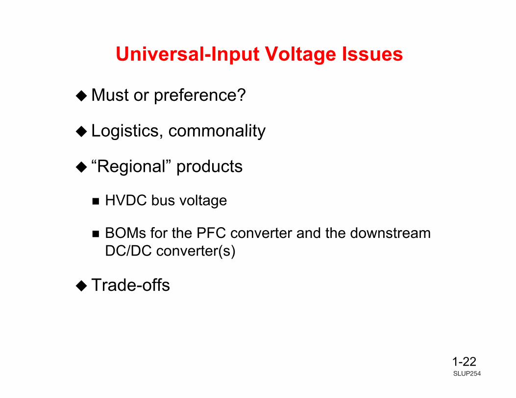
Universal-Input Voltage Issues
Must or preference?
Logistics commonalityLogistics, commonality
“Regional” products
HVDC bus voltage
BOM f th PFC t d th d tBOMs for the PFC converter and the downstream DC/DC converter(s)
Trade-offs
1-22
SLUP254
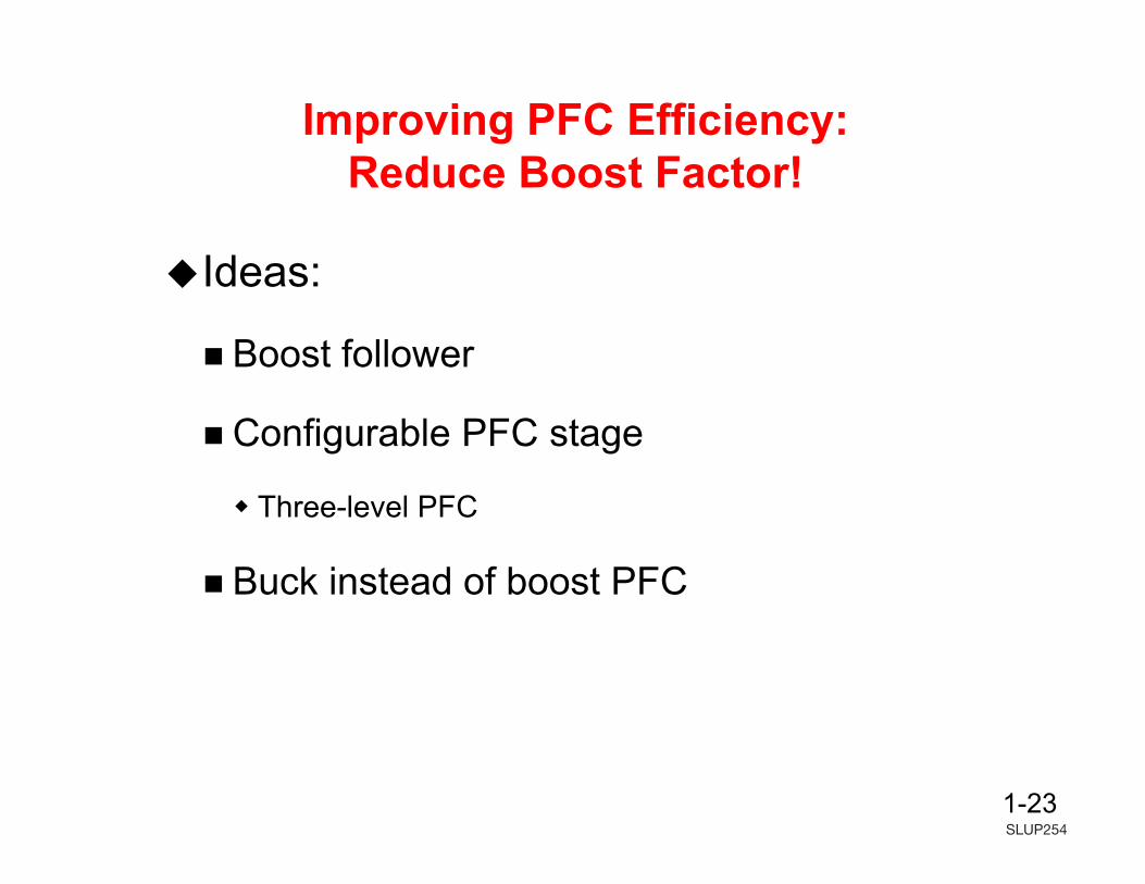
Improving PFC Efficiency: Reduce Boost Factor!educe oost acto
Ideas:
Boost follower
Configurable PFC stage
Three level PFCThree-level PFC
Buck instead of boost PFC
1-23

SLUP254
Boost-Follower PFCO t t V lt (C ti l)
3.5
400
300V)
Output Voltage (Conventional)
e (Boost Follower)3
2 5r (B
F)
Volta
ge ( V
200Output Voltage (B
Input Voltage
2.5
Boo
st F
acto
r
2
ConventionalBoost PFC
100
0100 20 30 40 50 60 70 80 90 100
B
1.5
1100 150 200 250
Boost-Follower PFC
Conventional PFC maintains same output voltage for different
100 20 30 40 50 60 70 80 90 100Time (ms)
100 150 200 250Input Voltage, V (V)in
line voltages, the boost factor is 3.3 at 85-V inputBoost follower PFC changes its output voltage according to the AC line voltage (following AC line voltage)
1-24
Boost factor is greatly reduced and efficiency can be improved but Vout is not constant

SLUP254
Boost-Follower PFC Implementation
By adjusting the voltage-sensing divider network, output voltage can be changed with most off-the-shelf PFC controllersPFC controllers
UCC3817
RectifiedLine Voltage
V(Boost Output
Voltage)
out
UCC3817PFC Controller
VoltageAmplifier
R1998 kΩ
R3998 kΩ
Amplifier
Internal
R214.3 kΩ
R4Q1C1
+
–
ReferenceR439.2 kΩ
R539.2 kΩ
2N22226.6 µF
1-25“Simple circuitry gets that old PFC controller working in a boost-follower PFC Application,” By Michael O’Loughlin

SLUP254
Design Considerations
“Boost Follower” reduces BF but:T f t ti i th d tTransformer turns ratio in the downstream converters must be lower, so:
Primary currents are higher, VA rating increases
Higher voltages on rectifiers, higher Vf
Larger filter inductor
Larger capacitors on the HV busLarger capacitors on the HV bus
1-26

SLUP254
Configurable Topologies
Use identical components for both 115-V and 230-V inputs
Same HVDC bus voltage
C f fConfiguration on assembly line for 115 V or 230 V
Nearly equal efficiencies for 115-V or 230-V operation
1-27

SLUP254
“Ideal” Configurable PFCL li i t fi tiHi h li i t fi ti Low line-input configurationHigh line-input configuration
At high line input, the MOSFETs, diodes, and inductors are in
At low line input, the MOSFETs, diodes, and
series
Output voltage is equal to the peak of the high line voltage
inductors are in parallel
Output voltage is only half the peak of the high line p g g
(same as conventional PFC)
Equal stresses on the converter components at either “High” or “Low” line-input configuration!
p gvoltage
1-28
Low line-input configuration!

SLUP254
Boost Factor of Ideal Configurable PFC3 5
)
3
3.5
ConventionalBoost PFC Converter
ost F
acto
r (B
F)2.5
2
Boo
2
1.5
Ideal Configurable
Input Voltage, V (V)in
1100 150 200 250
gPFC Converter
At “high” line-input condition, the BF and the output voltage are the same as for a conventional PFCAt “low” line-input condition the BF and the output
1-29
At low line-input condition, the BF and the output voltage are half the values of a conventional PFC

SLUP254
“Real-Life” Solutions
The “ideal” circuit is not practical
Voltage balancing for series devices
D i i i it f i i itDriving circuit for series circuits
Practical circuits will be less efficient than the ideal
1-30

SLUP254
Configurable Three-Level PFC
High line-input condition: two boost PFCs are in series
Low line-input condition: only one boost PFC is operating at each half lineseries operating at each half line cycle
1-31Note: Output-bus voltage does not change for different configurations

SLUP254
Boost Factor and Efficiency Estimation3 5
F)
3
3.5
ConventionalBoost PFC Converter
98
%)
Boo
st F
acto
r (B
2.5
2
96
94
Effic
ienc
y, η
(
B
1.5
1100 150 200 250
Ideal ConfigurablePFC Converter
92
9050 100 150 200 250 300
Configurable three-level PFC maintains same output voltage for different line conditions
Input Voltage, V (V)in
100 150 200 250 50 100 150 200 250 300Input Voltage, V (V)in
At low line input, each boost PFC operates half-line cycle and the equivalent output voltage is half of the total PFC output voltage
1-32
gThis reduced output voltage reduces the boost factor at low line input and improves efficiency

SLUP254
Benefits and Challenges
Benefits
Reduced boost factor improves overall system efficiency
Three-level structure, a lower-voltage switches and diodes can be used to improve efficiency
At low line conditions, the bridge is reconfigured as a doubler (bridge diodes can be paralleled)
ChallengesChallenges
At low line input, each boost PFC only operates half of the line cycle (component utilization)cycle (component utilization)
Devices referenced to different grounds: drive, current sensing
Voltage balancing on the output capacitors
1-33
Voltage balancing on the output capacitors

SLUP254
The Buck PFC
A buck converter can also shape the input currentHandles least power at lowest input (“Buck Factor”)
Iin
Vboost+
+
Outboost
––
Control(Modified(Modified
Peak CMC)
1-34

SLUP254
Idealized AC-Line Current with a Buck PFCt a uc C
1.51.000.5
0–0.5
1 0I
(A)
loadLow Line Input
(Normalized input t) –1.0
–1.50 5 10 15 20
Time (ms)
current)
1.51.00 5A
) 0.50
–0.5–1.0
I (A
loadHigh Line Input
(Normalized input current)
1-35
–1.50 5 10 15 20
Time (ms)

SLUP254
Buck PFC and Prevailing Standards
The buck PFC draws current only if the input voltage is higher than the output voltagevoltage is higher than the output voltage
The optimal output voltage for universal input voltage is 80 V
Waveform is “ugly” – but passes both EPAWaveform is ugly – but passes both EPA and IEC standards
1-36

SLUP254
Benefits of the Buck PFC
Solves the problem of low efficiency at low input voltage
Allows optimization of the downstream DC/DC converter
Inherent inrush-current control
“Gentler” on the HV diode than the boost converter it replaces
1-37

SLUP254
Efficiency of a 90-W Buck PFC versus the AC-Input Voltagee sus t e C put o tage
9896969492(%
)
9088
ficie
ncy
(
868482
Eff
8280
90 130110 170 190150 210 230 250 270AC Input (V)
1-38
p ( )

SLUP254
Conclusions
PFC provides many benefits but adds losses that are strongly affected by the Boost Factor
Reconfigurable-PFC topology is available that can reduce the effective BF and use the same components for both 115-V and 230-V lines—components for both 115 V and 230 V linesothers to be invented?
It remains to be seen if the pressure for ever higher e a s o be see e p essu e o e e g eefficiency will drive adoption of more complex topologies
The buck PFC is an attractive solution for universal input voltages at power levels below 600 W
1-39

SLUP282
TI Worldwide Technical Support
InternetTI Semiconductor Product Information Center Home Pagesupport.ti.com
TI E2E™ Community Home Pagee2e.ti.com
Product Information CentersAmericas Phone +1(972)644-5580
Brazil Phone 0800-891-2616
Mexico Phone 0800-670-7544
Fax +1(972)927-6377 Internet/Email support.ti.com/sc/pic/americas.htm
Europe, Middle East, and AfricaPhone EuropeanFreeCall 00800-ASK-TEXAS (0080027583927) International +49(0)8161802121 RussianSupport +7(4)959810701
Note:TheEuropeanFreeCall(TollFree)numberisnotactiveinallcountries.Ifyouhavetechnicaldifficultycallingthefreecallnumber,pleaseusetheinternationalnumberabove.
Fax +(49)(0)8161802045Internet support.ti.com/sc/pic/euro.htmDirectEmail [email protected]
JapanPhone Domestic0120-92-3326
Fax International+81-3-3344-5317 Domestic0120-81-0036
Internet/Email Internationalsupport.ti.com/sc/pic/japan.htm Domesticwww.tij.co.jp/pic
A122010
Important Notice:TheproductsandservicesofTexasInstrumentsIncorporatedanditssubsidiariesdescribedhereinaresoldsubjecttoTI’sstandardtermsandconditionsofsale.CustomersareadvisedtoobtainthemostcurrentandcompleteinformationaboutTIproductsandservicesbeforeplacingorders.TIassumesnoliabilityforapplicationsassistance,customer’sapplicationsorproductdesigns,softwareperformance,orinfringementofpatents.Thepublicationofinformationregardinganyothercompany’sproductsorservicesdoesnotconstituteTI’sapproval,warrantyorendorsementthereof.
AsiaPhone International +91-80-41381665 Domestic Toll-FreeNumber Note:Toll-freenumbersdonotsupport
mobileandIPphones. Australia 1-800-999-084 China 800-820-8682 HongKong 800-96-5941 India 1-800-425-7888 Indonesia 001-803-8861-1006 Korea 080-551-2804 Malaysia 1-800-80-3973 NewZealand 0800-446-934 Philippines 1-800-765-7404 Singapore 800-886-1028 Taiwan 0800-006800 Thailand 001-800-886-0010Fax +8621-23073686Email [email protected]@ti.comInternet support.ti.com/sc/pic/asia.htm
TheplatformbarandE2EaretrademarksofTexasInstruments.Allothertrademarksarethepropertyoftheirrespectiveowners.

IMPORTANT NOTICE
Texas Instruments Incorporated and its subsidiaries (TI) reserve the right to make corrections, enhancements, improvements and otherchanges to its semiconductor products and services per JESD46, latest issue, and to discontinue any product or service per JESD48, latestissue. Buyers should obtain the latest relevant information before placing orders and should verify that such information is current andcomplete. All semiconductor products (also referred to herein as “components”) are sold subject to TI’s terms and conditions of salesupplied at the time of order acknowledgment.TI warrants performance of its components to the specifications applicable at the time of sale, in accordance with the warranty in TI’s termsand conditions of sale of semiconductor products. Testing and other quality control techniques are used to the extent TI deems necessaryto support this warranty. Except where mandated by applicable law, testing of all parameters of each component is not necessarilyperformed.TI assumes no liability for applications assistance or the design of Buyers’ products. Buyers are responsible for their products andapplications using TI components. To minimize the risks associated with Buyers’ products and applications, Buyers should provideadequate design and operating safeguards.TI does not warrant or represent that any license, either express or implied, is granted under any patent right, copyright, mask work right, orother intellectual property right relating to any combination, machine, or process in which TI components or services are used. Informationpublished by TI regarding third-party products or services does not constitute a license to use such products or services or a warranty orendorsement thereof. Use of such information may require a license from a third party under the patents or other intellectual property of thethird party, or a license from TI under the patents or other intellectual property of TI.Reproduction of significant portions of TI information in TI data books or data sheets is permissible only if reproduction is without alterationand is accompanied by all associated warranties, conditions, limitations, and notices. TI is not responsible or liable for such altereddocumentation. Information of third parties may be subject to additional restrictions.Resale of TI components or services with statements different from or beyond the parameters stated by TI for that component or servicevoids all express and any implied warranties for the associated TI component or service and is an unfair and deceptive business practice.TI is not responsible or liable for any such statements.Buyer acknowledges and agrees that it is solely responsible for compliance with all legal, regulatory and safety-related requirementsconcerning its products, and any use of TI components in its applications, notwithstanding any applications-related information or supportthat may be provided by TI. Buyer represents and agrees that it has all the necessary expertise to create and implement safeguards whichanticipate dangerous consequences of failures, monitor failures and their consequences, lessen the likelihood of failures that might causeharm and take appropriate remedial actions. Buyer will fully indemnify TI and its representatives against any damages arising out of the useof any TI components in safety-critical applications.In some cases, TI components may be promoted specifically to facilitate safety-related applications. With such components, TI’s goal is tohelp enable customers to design and create their own end-product solutions that meet applicable functional safety standards andrequirements. Nonetheless, such components are subject to these terms.No TI components are authorized for use in FDA Class III (or similar life-critical medical equipment) unless authorized officers of the partieshave executed a special agreement specifically governing such use.Only those TI components which TI has specifically designated as military grade or “enhanced plastic” are designed and intended for use inmilitary/aerospace applications or environments. Buyer acknowledges and agrees that any military or aerospace use of TI componentswhich have not been so designated is solely at the Buyer's risk, and that Buyer is solely responsible for compliance with all legal andregulatory requirements in connection with such use.TI has specifically designated certain components as meeting ISO/TS16949 requirements, mainly for automotive use. In any case of use ofnon-designated products, TI will not be responsible for any failure to meet ISO/TS16949.
Products ApplicationsAudio www.ti.com/audio Automotive and Transportation www.ti.com/automotiveAmplifiers amplifier.ti.com Communications and Telecom www.ti.com/communicationsData Converters dataconverter.ti.com Computers and Peripherals www.ti.com/computersDLP® Products www.dlp.com Consumer Electronics www.ti.com/consumer-appsDSP dsp.ti.com Energy and Lighting www.ti.com/energyClocks and Timers www.ti.com/clocks Industrial www.ti.com/industrialInterface interface.ti.com Medical www.ti.com/medicalLogic logic.ti.com Security www.ti.com/securityPower Mgmt power.ti.com Space, Avionics and Defense www.ti.com/space-avionics-defenseMicrocontrollers microcontroller.ti.com Video and Imaging www.ti.com/videoRFID www.ti-rfid.comOMAP Applications Processors www.ti.com/omap TI E2E Community e2e.ti.comWireless Connectivity www.ti.com/wirelessconnectivity
Mailing Address: Texas Instruments, Post Office Box 655303, Dallas, Texas 75265Copyright © 2015, Texas Instruments Incorporated