Efficient organic–inorganic intumescent interfacial flame ...

1
High Performance Inverted Organic Photovoltaics Without
Hole Selective Contact.
Achilleas Savva*, Ignasi Burgués-Ceballos, Giannis Papazoglou and Stelios A.
Choulis*.
Molecular Electronics and Photonics Research Unit, Department of Mechanical
Engineering and Materials Science and Engineering, Cyprus University of Technology,
Limassol, 3603 (Cyprus).
*email: [email protected], *email: [email protected]
ABSTRACT
A detailed investigation of the functionality of inverted organic photovoltaics (OPVs)
using bare Ag contacts as top electrode is presented. The inverted OPVs without hole
transporting layer (HTL) exhibit a significant gain in hole carrier selectivity and power
conversion efficiency (PCE) after exposure in ambient conditions. Inverted OPVs
comprised of ITO/ZnO/poly(3-hexylthiophene-2,5-diyl):phenyl-C61-butyric acid
methyl ester (P3HT:PCBM)/Ag demonstrate over 3.5% power conversion efficiency
only if the devices are exposed in air for over 4 days. As concluded through a series of
measurements, the oxygen presence is essential to obtain fully operational solar cell
devices without HTL. Moreover, accelerated stability tests under damp heat conditions
(RH=85% and T=65oC) performed to non-encapsulated OPVs demonstrate that HTL-
free inverted OPVs exhibit comparable stability to the reference inverted OPVs.
Importantly, it is shown that bare Ag top electrodes can be efficiently used in inverted
OPVs using various high performance polymer:fullerene bulk heterojunction material
systems demonstrating 6.5% power conversion efficiencies.

2
1. INTRODUCTION
Solution-based thin film photovoltaics based on organic semiconducting
materials have attracted remarkable interest as a possible alternative to conventional,
inorganic photovoltaic technologies. Newly synthesized organic semiconductors, as
well as novel interfacial engineering and electrode configurations continuously push
power conversion efficiency (PCE) of these photovoltaic devices over 10%.1-2
Typically, in all aforementioned device structures, the absorber is sandwiched
between two electrodes, each one selectively extracting one type of charge carrier. The
selectivity of the electrodes is a crucial factor for high device performance and is
typically provided by the implementation of sophisticated electrodes comprised by
charge selective contacts between the absorber and the metallic terminals of the device.
The normal structure is usually based on: ITO/poly(3,4-ethylene
dioxythiophene):poly(styrenesulfonate) (PEDOT:PSS)/photoactive layer/low work
function (LWF) metal (i.e. Al).3 In inverted structured OPVs the current flow is
reversed by changing the polarity of the electrodes and is normally based on: ITO/ n-
type metal oxides (i.e. TiOx4 or ZnO5 or n-doped metal oxides6)/photoactive layer/high
work function (HWF) metal (i.e. Ag)
Lifetime is an equally important factor relevant to product development targets
of OPVs. It has been proven that electrodes are one of the main origins of failure of
OPVs under harsh environmental conditions.7 The use of LWF metal based cathodes is
a main degradation factor related to electrodes stability, since LWF metals (Li, Ca, Al)
are oxidized extremely fast. Several strategies to improve the stability of normal
structured OPVs have been proposed such as the addition of metal nanoparticles within
the active layer8-9 as well as the implementation of more stable interfacial layers.10-11
3
On the other hand, inverted solution based PVs provide a facile and reliable
strategy to improve OPV stability, due to the implementation of HWF, more stable
metals (i.e. Ag) as top electrode.12 Despite the enhanced lifetime of the inverted
structured compared with normal structured OPVs, it has been proven that a major
origin of failure of inverted OPVs is due to the most commonly used hole selective
contact PEDOT:PSS.13 Its hygroscopic and acidic nature results in insufficient hole
selectivity of the top electrode over time of exposure under harsh environmental
conditions.14-15 In addition, we have recently proved that not only the hygroscopic
nature of PEDOT:PSS, but also the poor adhesion between the PEDOT:PSS and the
polymeric active layer materials of inverted OPVs is another mechanism of degradation
of inverted OPVs under intense humidity conditions.16 In addition, a number of studies
prove that major degradation mechanisms of inverted OPVs arise from the interfaces
formed between the top electrode components and the active layer when PEDOT:PSS
is used.17-18
Based on the latter, promising replacements and currently investigated
substitutes for PEDOT:PSS come from the class of metal oxides, due to their excellent
optoelectronic properties and chemical/moisture resistance. Metal oxides such as
WO3,19 MoO3,
20 V2O5,21 have been used as efficient hole selective contacts in inverted
OPVs. This novel buffer layer engineering, results in optimum inverted OPVs
electrodes selectivity, leading in high Fill Factors (FF) over 65%,22 and in some cases
in enhanced lifetime performance.23
Interestingly, recent studies report that the electrodes of inverted OPVs could
provide the necessary charge selectivity without the use of charge selective contacts.
J.-C.Wang et al. reported an efficient inverted OPV device in which an electron
selective layer was not used.24 The inverted OPVs with bare ITO bottom electrodes

4
demonstrated high electron selectivity after a UV light treatment. In addition, M.S.
white et al. demonstrated that inverted OPVs using bare Ag top contacts could
efficiently serve as hole selective electrode for inverted OPVs.25 Further studies
analyzed the phenomenon and observed that inverted OPVs showed an increase in PCE
after exposure of the devices in air.26 The increase in PCE was attributed to the
increased work function of Ag layers after the exposure in air. TOF-SIMs studies
showed the presence of significantly increased silver oxide percentage at the interface
of Ag with the P3HT:PCBM layer.27
In this report a detailed investigation of the functionality of inverted OPVs using
bare Ag contacts as the hole selective top electrode is provided. Initially, inverted OPVs
comprised of ITO/ZnO/P3HT:PCBM/PEDOT:PSS/Ag (reference inverted OPVs) are
compared with ITO/ZnO/P3HT:PCBM/Ag (HTL-free inverted OPVs). These devices
are measured after exposure in air for several days after fabrication. It is demonstrated
that HTL-free devices are continuously gaining in PCE and finally reaching the PCE
levels of the reference inverted OPVs. To investigate the impact of atmospheric
conditions in the hole selectivity process encapsulated and non-encapsulated HTL-free
devices are compared during several days after exposure in air. The oxygen presence is
essential to obtain fully operational solar cell devices. This effect is verified through a
series of measurements and calculations such as current vs voltage characteristics, Vbi
calculations, statistical analysis and photocurrent mapping measurements. Accelerated
stability tests under damp heat conditions (RH=85% and T=65oC) performed in non-
encapsulated devices demonstrated that HTL-free inverted OPVs exhibit comparable
stability compared with reference inverted OPVs (using PEDOT: PSS) at least for the
first 200 hours of testing. Finally, bare Ag top electrodes under the presence of suitable
oxygen treatment are proved to be functional using different high performance
5
polymer-fullerene active layer material systems such as PTB7:PC[70BM], and PTB7-
TH:PC[70]BM demonstrating HTL-free inverted OPVs with 6.5% PCE .
2. MATERIALS AND METHODS
Materials: Pre-patterned glass-ITO substrates (sheet resistance 4Ω/sq) were purchased
from Psiotec Ltd. Zinc acetate dehydrate, 2-methoxyethanol and ethanolamine have
been purchased from Sigma Aldrich, P3HT from Rieke metals, PTB7 from 1-material,
PTB7-Th from Solarmer, PC[60]BM and PC[70]BM from Solenne BV and
PEDOT:PSS PH from H.C. Stark. Device Fabrication: For inverted solar cells, ITO
substrates were sonicated in acetone and subsequently in isopropanol for 10 minutes.
ZnO electron transporting layer was prepared using a sol-gel process as described in
detail in our previous study.6 The photo-active layer, deposited on top of ZnO, consisted
of a) a blend of P3HT:PC60BM (1:0.8 wt%) 36 mg/ml in chlorobenzene, doctor bladed
in air, with a resulting thickness of ~180 nm, b) a blend of PTB7:PC70BM (1:1.5) 25
mg/mL in chlorobenzene with 3% of 1,8-diiodooctane (DIO) additive, doctor bladed in
air with a resulting thickness of ~90 nm without further annealing, or c) a blend of
PTB7-Th:PC70BM (1:2) 36 mg/mL in o-dichlorobenzene with 2.5% of DIO additive,
spin coated in glove box, ~90 nm thick, slow dried in a petri dish for 1h. For inverted
OPVs containing PEDOT:PSS a treatment with two wetting agents was applied as
described in detail previously.28 All the inverted OPVs based on P3HT:PCBM were
annealed inside a glove box at 140 °C for 20 minutes. The devices were completed by
thermal evaporating a silver layer with a thickness of 100 nm. Encapsulation was
applied directly after evaporation in the glove box using an Ossila E131 encapsulation
epoxy resin activated by 365nm UV-irradiation and a glass coverslip. The active area
of the devices was 9 mm2. Storage: During the study the samples were stored under two
6
different conditions, namely 1) exposure to air and 2) exposure to pure oxygen. For the
latter the samples were stored in a desiccator, to which subsequential vacuum and
refilling with pure oxygen (99.5%) were performed. Accelerated degradation: The un-
encapsulated inverted OPVs were subjected to degradation under the ISOS D-3
protocol (Damp Heat test, RH = 85%, T = 65 °C, Dark conditions) using a climate
chamber. Characterization: The thicknesses of the active layers were measured with a
Veeco Dektak 150 profilometer. The current density-voltage (J/V) characteristics were
measured with a Keithley source measurement unit (SMU 2420). For illumination, a
calibrated Newport Solar simulator equipped with a Xe lamp was used, providing an
AM1.5G spectrum at 100mW/cm2 as measured by an oriel 91150V calibration cell
equipped with a KG5 filter. Net photocurrent vs voltage characteristics were obtained
by extracting the dark from the illuminated J/V characteristics. Photocurrent and open
circuit voltage (Voc) mapping measurements were performed under 405 nm laser
excitation using a Botest PCT photocurrent system.
3. RESULTS AND DISCUSSION
Inverted OPVs comprised of ITO/ZnO/P3HT:PCBM/ PEDOT:PSS/Ag
(reference inverted OPVs) are compared with ITO/ZnO/ P3HT:PCBM/Ag (HTL-free
inverted OPVs) and shown in figure 1a. The inverted OPVs under study were tested
directly after fabrication with no encapsulation barrier, stored in ambient conditions
and tested periodically up to 7 days after fabrication. To avoid repetitions within the
rest of the manuscript the process of exposing in ambient conditions of all the inverted
OPVs under study 2, 4 and 7 days after fabrication will be referred as day 2, 4 and 7,
respectively. Figure 1 b) c) and d) show representative J/V characteristics for the
inverted OPVs under study out of total 8 inverted OPV devices in each case. Similar

7
results were observed in more than 5 identically executed experimental runs (over 40
devices for each case).
Figure 1. a) the inverted OPVs structure and materials used in this study, b) current
density versus voltage characteristics under illumination and c) under dark conditions,
d) net photocurrent density versus voltage measurements.
Figure 1b shows the current density vs voltage characteristics of all of the non-
encapsulated inverted OPVs under study obtained from day 0 to day 7. Reference
inverted OPVs exhibited good cell operation directly after fabrication. This good
performance was also maintained upon exposure of reference devices in air after 2, 4
and 7 days, respectively. On the other hand, non-encapsulated HTL-free inverted OPVs
exhibited poor device performance after fabrication with low Voc and FF factor values
and thus limited initial PCE values. Interestingly, these HTL-free devices were
continuously gaining in Voc, FF and PCE after the exposure of the devices in air and
finally reaching the PCE levels of the reference inverted OPVs.

8
These observations are also in agreement with figure 1c, in which the J/V
characteristics under dark conditions for all the inverted OPVs under study are shown.
Functionality of non-encapsulated HTL-free inverted OPVs improved gradually from
day 0 to day 7. This enhancement could be mainly attributed to a drastic decrease of
the series resistance (Rs) and secondary to parallel resistance (Rp) increase from day 0
to day 7 respectively. At day 7 non-encapsulated HTL-free inverted OPVs show good
hole selectivity since the device internal resistances, FF and PCE exhibit good values,
very similar to the reference inverted OPVs. The latter, clearly demonstrates a
functional hole selective top electrode for inverted OPVs, using only Ag without HTL.
The values of Rs and Rp for all the representative diodes under study were calculated
using a simulation model described previously by Waldauf et al29 and shown in table
1.
In an attempt to better understand the origin of the functionality of the bare Ag
electrodes of inverted OPVs, the Vbi of all the inverted OPVs under study were
calculated. Figure 1d shows the net photocurrent density as a function of diode bias for
the three inverted OPVs under study. These measurements can be used to determine the
built-in potential (Vbi) and thus the changes in the energy barriers at the interfaces
between the active layer and the electrodes.30 As table 1 shows, the Vbi for HTL-free
inverted OPVs increased gradually over exposure in air from 0.16 V after fabrication
to 0.52 V in day 4 and 0.65 V in day 7. The Vbi of HTL-free inverted OPVs at day 7 is
very similar with the corresponding 0.67 V of the reference inverted OPVs using
PEDOT:PSS hole selective contact directly after fabrication. All the critical device
parameters of the representative inverted OPVs under study are shown in table 1.

9
Table 1. Summary of the photovoltaic parameters of all the inverted OPVs under
study calculated from figure 1.
From day 1 to 7 the most important changes in the device are the Voc, Vbi and the Rs.
It could be deduced that at day 0 an energy barrier at the P3HT:PCBM/Ag interface is
present, according to the high Rs and low Vbi. Over days of exposure this barrier is
reduced, leading to continuously lower Rs, higher Vbi and Voc and thus increased hole
selectivity, FF and PCE values. The origin of this barrier is attributed to a reduction of
Ag work function. The work function of Ag has been documented to be located at −4.3
eV.31 However, it has been shown that exposure to oxygen can induce a shift in band
alignment at metal/organic interfaces.31 Based on the efficient hole-collecting nature of
the P3HT/Ag interface seen here, it is evident that a similar shift further from vacuum
is occurring upon contact of the two materials with the presence of oxygen.
To proof that oxygen is the only component causing the modification of the
silver electrode we compared HTL-free inverted OPVs exposed to ambient air with
HTL-free inverted OPVs exposed to >99% oxygen atmosphere (supplementary figure
S1). We observed that HTL-free inverted OPVs exposed to oxygen only environment
became functional at day 7, following the same trend as those exposed to ambient air.
Inverted
OPVs
Voc
[V]
Jsc
[mA/cm2]
FF
[%]
PCE
[%]
Rp
[Ohm]
Rs
[Ohm]
Vbi
[V]
Reference after fab. 0.59 8.71 64.5 3.34 2795 0.62 0.67
HTL-free after fab. 0.16 7.25 32.7 0.37 470 150 0.16
HTL-free at Day 2 0.31 8.64 37.5 0.99 1271 1.16 0.31
HTL-free at Day 4 0.50 9.10 48.0 2.18 1558 1.0 0.52
HTL-free at Day7 0.57 9.33 64.8 3.45 1570 1.1 0.65
10
This suggests that the presence of oxygen is crucial in this process. According to our
results, water and other gases present might play a minor role.
Although Ag band alignment with the P3HT interface could serve as a hole
transporting material, it would be unlikely to also provide electron blocking capabilities
and thus the high FF values observed in HTL-free devices is most likely related to
changes in interfacial properties. It has been previously reported that upon air exposure,
there is a pronounced increase of AgO and Ag2O signals at the Ag–organic interface.27
The presence of an oxide layer at the Ag–organic interface in the samples exposed to
oxygen can be used to justify the outstanding hole selectivity of the inverted OPVs with
no hole selective layer.
To further investigate the impact of oxygen in this process, inverted OPVs with
and without encapsulation were fabricated. Four series of inverted OPVs were tested in
this experimental run. Reference and HTL-free inverted OPVs were fabricated and
tested up to 7 days after fabrication, similar to what is described previously in this study.
Some of the HTL-free devices were encapsulated directly after fabrication in nitrogen
filled glovebox before the devices were exposed to oxygen (named as HTL-free
encapsulated after fab). Another set of HTL-free inverted OPVs were encapsulated after
being exposed 2 days in ambient conditions (HTL-free encapsulated after 2 days).
Figure 2 shows the box plots constructed out of 8 devices for each inverted OPV device
structure under study.

11
Figure 2. Average results represented in box plots out of 8 devices of each of the 4
series of inverted OPVs under study, reference inverted OPVs (black box plots), non-
encapsulated HTL-free inverted OPVs (red box plots), encapsulated after fabrication
HTL-free inverted OPVs (green box plots) and encapsulated 2 days after fabrication
and exposure in air HTL-free inverted OPVs (blue box plots). a) Open circuit voltage
(Voc) b) current density (Jsc) c) fill factor (FF) and d) power conversion efficiency
(PCE).
Reference inverted OPVs with PEDOT:PSS hole selective contact
demonstrated good functionality directly after fabrication and well maintained up to
day 7. On the other hand, all the HTL-free un-encapsulated inverted OPVs
demonstrated very low Voc, FF and PCE values after fabrication. Under ambient
exposure these devices showed a significant increase mainly in Voc. FF parameter is
also improved and thus PCE values are greatly increased. In contrast, HTL-free OPVs

12
encapsulated after fabrication did not gain in PCE from day 1 to day 7, exhibiting very
low Voc, FF and PCE values. This is a strong indication that the presence of oxygen is
necessary for gaining in hole selectivity and thus PCE. As a further confirmation to the
above effects, HTL-free inverted OPVs encapsulated 2 days after fabrication exhibited
an increase in the first 2 days (when atmospheric oxygen is present) but after
encapsulation this gaining stops and the PCE is “frozen” at the values measured just
before the encapsulation process in day 2. This observation proves that the oxygen
presence is necessary for over 5 days in order to obtain fully operational inverted OPVs
using bare Ag hole selective electrodes. It is worthy to note here that similar results
have been observed in several other experimental runs. In addition, we observed that
non-encapsulated devices stored in a nitrogen filled glovebox (instead of ambient
conditions) did not convert into fully operational devices even after several days
(devices were periodically measured but data are not shown within the manuscript).
This is another proof that the oxygen presence is a crucial factor in functionalizing the
hole selective electrode.
In order to examine whether the observed effect is reversible, 8 HTL-free
devices fully functional (after exposure to air) were subjected to a 10-3 bar vacuum for
3 hours. As demonstrated in supplementary figure S2b the inverted OPVs do not loose
in functionality after exposure under vacuum. This indicates that the observed effect is
not reversible. In addition, another set of 8 HTL-free inverted OPVs were reversed
engineered by removing the silver layer on top after the inverted OPVs became fully
functional at day 7. After that, a fresh layer of Ag was evaporated on top of the
ITO/ZnO/P3HT:PCBM. The aforementioned HTL-free inverted OPVs exhibited
similar diode behavior with that of day 0 (low Voc and PCE). These results (see figure
S2b in supplementary information) indicate that the observed effect originates from the

13
Ag layer interaction with oxygen and not from any other interaction between the layers
of the device.
To better analyze the phenomenon, spatially resolved Voc and photocurrent
measurements were performed over the whole area of all the inverted OPVs under
study. Figure 3 shows the Voc maps of the representative reference inverted OPVs
directly after fabrication and HTL-free inverted OPVs after fabrication, at day 2 and at
day 7.
Figure 3. Voc maps at 405nm laser excitation of a) reference inverted OPVs after
fabrication, b) non-encapsulated HTL-free inverted OPVs after fabrication, c) non-
encapsulated HTL-free inverted OPVs 2 days after fabrication and d) non-encapsulated
HTL-free inverted OPVs 7 days after fabrication. The active area of all the inverted
OPVs under study is 9 mm2 and is highlighted with a dashed black square.
a) Reference (PEDOT) After Fab
-2 -1 0 1
-1
0
1
2
X position (mm)
Y p
ositio
n (
mm
)
0.1000
0.1960
0.2920
0.3880
0.4840
0.5800
Voltage (V) -2 -1 0 1
-2
-1
0
1
X position (mm)
Y p
ositio
n (
mm
)
0.1000
0.1960
0.2920
0.3880
0.4840
0.5800
Voltage (V)
b) HTL-free After Fabrication
-1 0 1 2-2
-1
0
1
2
X position (mm)
Y p
ositio
n (
mm
)
0.1000
0.1960
0.2920
0.3880
0.4840
0.5800
Voltage (V)
c) HTL-free 2 days After Fabrication
-1 0 1 2-2
-1
0
1
2
X position (mm)
Y p
ositio
n (
mm
)
0.1000
0.1960
0.2920
0.3880
0.4840
0.5800
Voltage (V)
d) HTL-free 7 days After Fabrication

14
Reference inverted OPVs (figure 3a) showed a well distributed Voc within the
device directly after fabrication. Interestingly, HTL-free inverted OPVs after
fabrication showed a poor Voc only at one edge of the device. Testing the same inverted
OPV at day 2 revealed an intense Voc at the edges and moving to the center of the
device. Finally, at day 7 the Voc is well distributed all over the 9 mm2 of the device.
Consistently, photocurrent maps (see Fig. S3 in supplementary information) follow a
similar trend as Voc. These measurements undoubtedly demonstrate that the process
takes place from the edges to the center of the HTL-free devices. We believe that this
is linked with our previous observations concerning the impact of oxygen in the HTL-
free inverted OPVs. The oxygen presumably penetrates the non-encapsulated inverted
OPVs from the edges of the device and the Voc and photocurrent are correspondingly
more intense at the edges at day 0 and 2. At day 7 the oxygen has diffused all over the
active area, causing a reduction in Ag work function and correspondingly a
homogeneous Voc and an efficient photocurrent generation due to enhanced top
electrode hole selectivity. These observations are in agreement with the assumptions
made in previously reported studies that the oxygen might diffuse from the sides of the
Ag electrodes rather than through the Ag layer.26
Another important factor for cost efficient OPVs is their long-term stability. It
is well known that electrodes are one of the major degradation mechanisms of inverted
OPVs.9a The inverted OPVs without any encapsulation barrier were subjected to
stability studies under the ISOS D-3 protocol using a climate chamber. Damp Heat test
(RH = 85% - T = 65 oC –Dark) is considered as one of the harshest test for OPVs and
it has been found to mainly affect the electrodes of inverted OPVs.7 Our reference
inverted OPVs (ITO/ZnO/P3HT:PCBM/PEDOT:PSS/Ag) were compared with
ITO/ZnO/P3HT:PCBM/Ag (HTL-free inverted OPVs). 12 non-encapsulated devices in

15
each case were examined. Figure 4 shows the average results of the normalized Voc,
Jsc, FF and PCE over time of damp heat exposure.
Figure 4. Lifetime performance under ISOS D-3 protocol (Damp heat, RH = 85%-Heat
65 oC -Dark) for reference non-encapsulated inverted OPVs ITO/ZnO/P3HT:PCBM/
PEDOT:PSS/Ag (black filled squares) and HTL-free non-encapsulated inverted OPVs
ITO/ZnO/P3HT:PCBM/Ag (open red circles). a) Normalized Voc, b) Normalized Jsc,
c) Normalized FF and d) Normalized PCE over time of exposure under damp-heat
conditions.
HTL-free inverted OPVs under damp heat conditions exhibited comparable
lifetime performance with inverted OPVs using a PEDOT:PSS. Both of the compared
inverted OPVs exhibit a significant drop in Jsc, FF and PCE in the first few hours. Later
on, the drop is smoother in both cases until the end of the study. Therefore, initial damp
16
heat tests prove that HTL-free inverted OPVs exhibit lifetime performances comparable
with inverted OPVs using a PEDOT:PSS as hole selective layers. However, a more
detailed lifetime investigation would be desirable in order to better examine the lifetime
behavior of these devices for more than 200 hours. To identify the exact degradation
mechanisms in each case deserves further studies and is beyond the scope of the present
work.
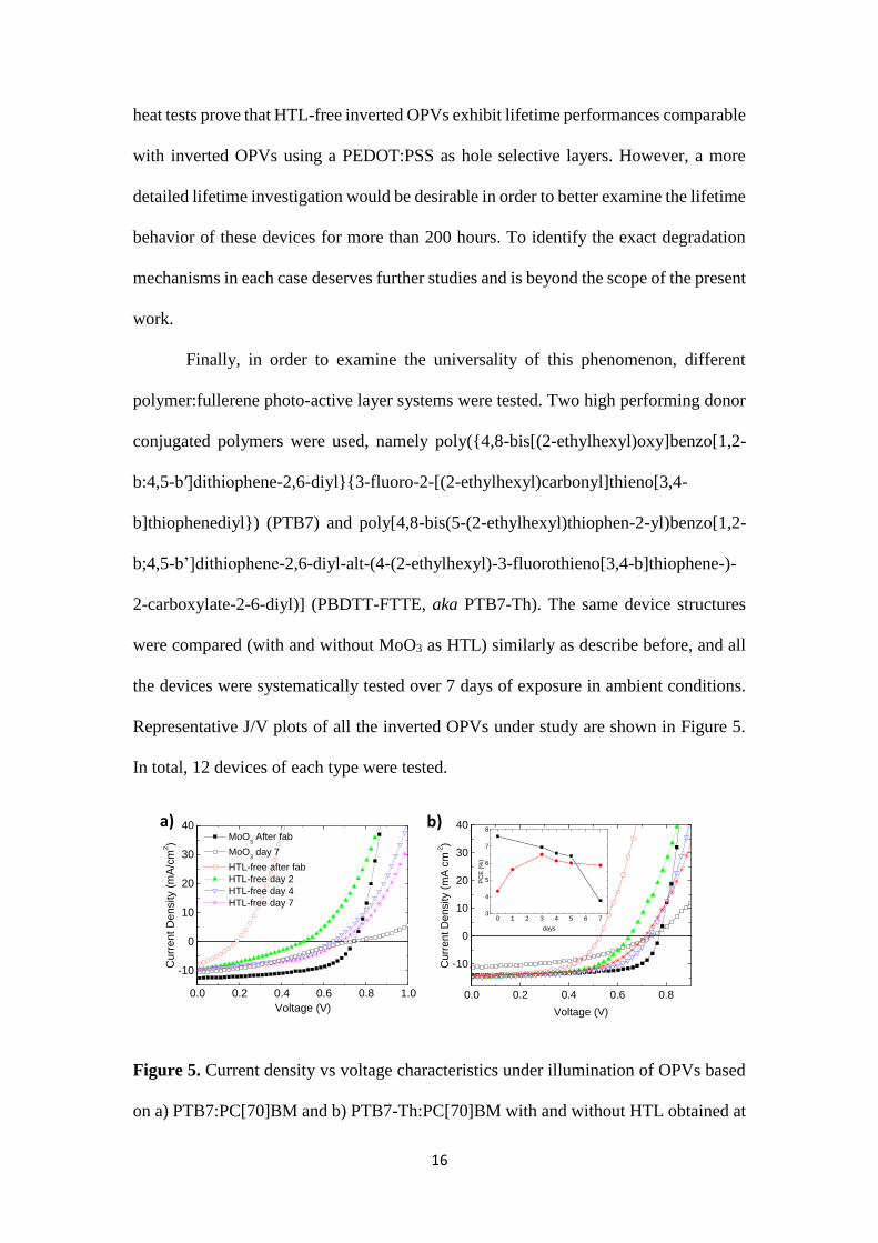
Finally, in order to examine the universality of this phenomenon, different
polymer:fullerene photo-active layer systems were tested. Two high performing donor
conjugated polymers were used, namely poly({4,8-bis[(2-ethylhexyl)oxy]benzo[1,2-
b:4,5-b′]dithiophene-2,6-diyl}{3-fluoro-2-[(2-ethylhexyl)carbonyl]thieno[3,4-
b]thiophenediyl}) (PTB7) and poly[4,8-bis(5-(2-ethylhexyl)thiophen-2-yl)benzo[1,2-
b;4,5-b’]dithiophene-2,6-diyl-alt-(4-(2-ethylhexyl)-3-fluorothieno[3,4-b]thiophene-)-
2-carboxylate-2-6-diyl)] (PBDTT-FTTE, aka PTB7-Th). The same device structures
were compared (with and without MoO3 as HTL) similarly as describe before, and all
the devices were systematically tested over 7 days of exposure in ambient conditions.
Representative J/V plots of all the inverted OPVs under study are shown in Figure 5.
In total, 12 devices of each type were tested.
Figure 5. Current density vs voltage characteristics under illumination of OPVs based
on a) PTB7:PC[70]BM and b) PTB7-Th:PC[70]BM with and without HTL obtained at
0.0 0.2 0.4 0.6 0.8 1.0
-10
0
10
20
30
40 MoO
3 After fab
MoO3 day 7
HTL-free after fab
HTL-free day 2
HTL-free day 4
HTL-free day 7
Cu
rre
nt
De
nsity (
mA
/cm
2)
Voltage (V)
a) b)
0.0 0.2 0.4 0.6 0.8
-10
0
10
20
30
40
Cu
rre
nt
De
nsity (
mA
cm
-2)
Voltage (V)
0 1 2 3 4 5 6 73
4
5
6
7
8
PC
E (
%)
days

17
different days of exposure in air. Inset in b) shows the evolution of PCE in devices with
(black squares) and without (red circles) HTL.
In the two material systems, reference inverted OPVs (with MoO3) exhibited
good diode behavior after fabrication demonstrating Voc = 0.74 V and 0.77 V, Jsc =
12.6 mA/cm2 and 14.1 mA/cm2, FF = 63% and 70% and PCE = 5.9% and 7.6% for
PTB7 and PTB7-Th based OPVs, respectively. On the other hand, HTL-free inverted
OPVs exhibited very poor performance after fabrication, similarly to what was
observed when using our reference P3HT:PCBM as the photo-active layer material
system. Over several days in exposure to air, HTL-free devices showed a gradual
increase in all the photovoltaic parameters. After 7 days, PTB7-based HTL-free devices
reached Voc = 0.68 V, Jsc = 9.5 mA/cm2, FF = 60% and PCE = 3.9%. In the case of
PTB7-Th HTL-free devices, only 3 days of exposure to air were needed to increase
efficiency from the initial 4.3% to a respectable PCE of 6.5%, with Voc = 0.73 V, Jsc
= 14.9 mA/cm2 and FF = 60%. In both cases, equivalently as in P3HT:PCBM samples,
the greatest enhancement corresponds to a significant increase in Voc, as can be clearly
seen in Figure 5. This indicates a reduction in Ag work function, as analyzed previously
within the text. Therefore, this phenomenon seems to be independent of the photo-
active materials. On the contrary, the PCE values of the HTL-free OPVs based on these
two high performing conjugated polymer donors did not match those of the reference
device. Inset in Figure 5b shows a constant decrease in the performance of reference
devices during the first 5 days, followed by a more abrupt decrease from there on. We
attribute the former to a gradual degradation of the photoactive layer, as these materials
are known to be not particularly air stable.32 The second step could be related to MoO3
degradation,33 which we have systematically observed in other material systems
containing MoO3 (this will be published separately). As a result, the progressive

18
increase of PCE in HTL-free devices upon exposure to air competes with the gradual
degradation of the active layer, as inset in Figure 5b reveals. Based on these
observations, we believe that bare Ag could serve as an efficient hole selective electrode
for a broad variety of active layer systems, particularly for those that show high air
stability.
4. CONCLUSIONS
In summary, functional inverted OPVs without hole selective contact are
investigated. It is shown that a crucial requirement to achieve sufficient hole selectivity
for inverted OPVs using bare Ag top electrodes is the exposure of the devices in
ambient conditions for several few days. As proven by detailed J/V analysis, the
inverted OPVs without hole selective contact are gaining gradually in Voc, FF and PCE
after exposure in ambient conditions. In contrast, HTL-free inverted OPVs which have
been encapsulated before any contact with atmospheric conditions do not convert into
operational diodes even after 7 days of exposure. Specifically, it is demonstrated that
the presence of oxygen is a key factor to achieve the desired hole selectivity and that
the process takes place from the edges to the center of the device. Progressive oxygen
ingress is assumed to partially oxidize the Ag layer in the interface with the active layer,
inducing changes in the work function of the electrode. Furthermore, damp heat test for
the air stable P3HT:PCBM material system proved that HTL-free non-encapsulated
inverted OPVs exhibit comparable lifetime with inverted non-encapsulated OPVs using
PEDOT:PSS/Ag hole selective electrode at least up to T80. Importantly, the
universality of this effect is demonstrated: bare Ag could be served as functional hole
selective electrodes not only in the P3HT:PCBM case but also in other highly efficient
polymer:fullerene systems such as PTB7:PCB[70]BM and PTB7-Th:PC[70]BM

19
leading in HTL-free inverted OPVs with PCE of 6.5%. We believe that the concept and
detailed investigation for HTL-free OPVs presented could be used for the evaluation of
air-stable novel materials simplifying the processing steps for high performance
inverted OPVs.
AKNOWLEDGEMENTS
This work has been funded by the H2020-ERC-2014-GoG project “Solution Processed
Next Generation Photovoltaics (Sol-Pro)” number 647311.
REFERENCES
1. Guo, X.; Zhou, N.; Lou, S. J.; Smith, J.; Tice, D. B.; Hennek, J. W.; Ortiz, R. P.;
Navarrete, J. T. L.; Li, S.; Strzalka, J.; Chen, L. X.; Chang, R. P. H.; Facchetti, A.;
Marks, T. J., Polymer Solar Cells With Enhanced Fill Factors. Nat. Photonics 2013, 7,
825-833.
2. You, J.; Dou, L.; Yoshimura, K.; Kato, T.; Ohya, K.; Moriarty, T.; Emery, K.; Chen,
C.-C.; Gao, J.; Li, G.; Yang, Y., A Polymer Tandem Solar Cell With 10.6% Power
Conversion Efficiency. Nat. Commun. 2013, 4, 1446.
3. Bai, S.; Cao, M.; Jin, Y.; Dai, X.; Liang, X.; Ye, Z.; Li, M.; Cheng, J.; Xiao, X.;
Wu, Z.; Xia, Z.; Sun, B.; Wang, E.; Mo, Y.; Gao, F.; Zhang, F., Low-Temperature
Combustion-Synthesized Nickel Oxide Thin Films as Hole-Transport Interlayers for
Solution-Processed Optoelectronic Devices. Adv. Energy Mater. 2014, 4, 1301460.
4. Waldauf, C.; Morana, M.; Denk, P.; Schilinsky, P.; Coakley, K.; Choulis, S. A.;
Brabec, C. J., Highly Efficient Inverted Organic Photovoltaics Using Solution Based
Titanium Oxide as Electron Selective Contact. Appl. Phys. Lett. 2006, 89, 233517.
20
5. Oh, H.; Krantz, J.; Litzov, I.; Stubhan, T.; Pinna, L.; Brabec, C. J., Comparison of
Various sol–gel Derived Metal Oxide Layers for Inverted Organic Solar Cells. Sol.
Energy Mater. Sol. Cells 2011, 95, 2194-2199.
6. Savva, A.; Choulis, S. A., Cesium-Doped Zinc Oxide as Electron Selective Contact
in Inverted Organic Photovoltaics. Appl. Phys. Lett. 2013, 102, 233301.
7. Reese, M. O.; Morfa, A. J.; White, M. S.; Kopidakis, N.; Shaheen, S. E.; Rumbles,
G.; Ginley, D. S. In Short-term metal/organic interface stability investigations of
organic photovoltaic devices, Photovoltaic Specialists Conference, 2008. PVSC '08.
33rd IEEE, 11-16 May 2008; 2008; pp 1-3.
8. Paci, B.; Generosi, A.; Albertini, V. R.; Spyropoulos, G. D., Stratakis, E.; Emmanuel
Kymakis, Enhancement of Photo/Thermal Stability of Organic Bulk Heterojunction
Photovoltaic Devices via Gold Nanoparticles Doping of the Active Layer. Nanoscale
2012, 4, 7452–7459.
9. Sygletou, M.; Kakavelakis, G.; Paci, B.; Generosi, A.; Kymakis, E.; Stratakis, E.,
Enhanced Stability of Aluminum Nanoparticle-Doped Organic Solar Cells, ACS Appl.
Mater. Interfaces 2015, 7, 17756−17764.
10. Kakavelakis, G.; Konios, D.; Stratakis, E.; Kymakis, E., Enhancement of the
Efficiency and Stability of Organic Photovoltaic Devices via the Addition of a Lithium-
Neutralized Graphene Oxide Electron-Transporting Layer Chem. Mater. 2014, 26,
5988−5993.
11. Yipa, H.-L.; Jen, A. K.-Y., Recent advances in solution-processed interfacial
materials for efficient and stable polymer solar cells. Energy Environ. Sci., 2012, 5,
5994-6011.
12. Reese, M. O.; Gevorgyan, S. A.; Jørgensen, M.; Bundgaard, E.; Kurtz, S. R.;
Ginley, D. S.; Olson, D. C.; Lloyd, M. T.; Morvillo, P.; Katz, E. A.; Elschner, A.;

21
Haillant, O.; Currier, T. R.; Shrotriya, V.; Hermenau, M.; Riede, M.; R. Kirov, K.;
Trimmel, G.; Rath, T.; Inganäs, O.; Zhang, F.; Andersson, M.; Tvingstedt, K.; Lira-
Cantu, M.; Laird, D.; McGuiness, C.; Gowrisanker, S.; Pannone, M.; Xiao, M.; Hauch,
J.; Steim, R.; DeLongchamp, D. M.; Rösch, R.; Hoppe, H.; Espinosa, N.; Urbina, A.;
Yaman-Uzunoglu, G.; Bonekamp, J.-B.; van Breemen, A. J. J. M.; Girotto, C.;
Voroshazi, E.; Krebs, F. C., Consensus Stability Testing Protocols for Organic
Photovoltaic Materials and Devices. Sol. Energy Mater. Sol. Cells 2011, 95, 1253-1267.
13. Norrman, K.; Madsen, M. V.; Gevorgyan, S. A.; Krebs, F. C., Degradation Patterns
in Water and Oxygen of an Inverted Polymer Solar Cell. J. Am. Chem. Soc. 2010, 132,
16883-16892.
14. Giannouli, M.; Drakonakis, V. M.; Savva, A.; Eleftheriou, P.; Florides, G.; Choulis,
S. A., Methods for Improving the Lifetime Performance of Organic Photovoltaics with
Low-Costing Encapsulation. ChemPhysChem 2015, 16, 1134-1154.
15. Drakonakis, V. M.; Savva, A.; Kokonou, M.; Choulis, S. A., Investigating
Electrodes Degradation in Organic Photovoltaics Through Reverse Engineering Under
Accelerated Humidity Lifetime Conditions. Sol. Energy Mater. Sol. Cells 2014, 130,
544-550.
16. Savva, A.; Georgiou, E.; Papazoglou, G.; Chrusou, A. Z.; Kapnisis, K.; Choulis, S.
A., Photovoltaic Analysis of the Effects of PEDOT:PSS-Additives Hole Selective
Contacts on the Efficiency and Lifetime Performance of Inverted Organic Solar Cells.
Sol. Energy Mater. Sol. Cells 2015, 132, 507-514.
17. Dupont, S. R.; Voroshazi, E.; Heremans, P.; Dauskardt, R. H., Adhesion Properties
of Inverted Polymer Solar Cells: Processing and Film Structure Parameters. Org.
Electron. 2013, 14, 1262-1270.

22
18. Jorgensen, M.; Norrman, K.; Gevorgyan, S. A.; Tromholt, T.; Andreasen, B.; Krebs,
F. C., Stability of Polymer Solar Cells. Adv. Mater. 2012, 24, 580-612.
19. Stubhan, T.; Li, N.; Luechinger, N. A.; Halim, S. C.; Matt, G. J.; Brabec, C. J.,
High Fill Factor Polymer Solar Cells Incorporating a Low Temperature Solution
Processed WO3 Hole Extraction Layer. Adv. Energy Mater. 2012, 2, 1433-1438.
20. Zilberberg, K.; Gharbi, H.; Behrendt, A.; Trost, S.; Riedl, T., Low-Temperature,
Solution-Processed MoO(x) for Efficient and Stable Organic Solar Cells. ACS Appl.
Mater. Interfaces 2012, 4, 1164-1168.
21. Meyer, J.; Hamwi, S.; Kroger, M.; Kowalsky, W.; Riedl, T.; Kahn, A., Transition
Metal Oxides for Organic Electronics: Energetics, Device Physics and Applications.
Adv. Mater. 2012, 24, 5408-5427.
22. Stubhan, T.; Ameri, T.; Salinas, M.; Krantz, J.; Machui, F.; Halik, M.; Brabec, C.
J., High Shunt Resistance in Polymer Solar Cells Comprising a MoO3 Hole Extraction
Layer Processed From Nanoparticle Suspension. Appl. Phys. Lett. 2011, 98, 253308.
23. Chen, C. P.; Chen, Y. D.; Chuang, S. C., High-Performance and Highly Durable
Inverted Organic Photovoltaics Embedding Solution-Processable Vanadium Oxides as
an Interfacial Hole-Transporting Layer. Adv. Mater. 2011, 23, 3859-3863.
24. Wang, J.-C.; Lu, C.-Y.; Hsu, J.-L.; Lee, M.-K.; Hong, Y.-R.; Perng, T.-P.; Horng,
S.-F.; Meng, H.-F., Efficient Inverted Organic Solar Cells Without an Electron
Selective Layer. J. Mater. Chem. 2011, 21, 5723-5728.
25. White, M. S.; Olson, D. C.; Shaheen, S. E.; Kopidakis, N.; Ginley, D. S., Inverted
Bulk-Heterojunction Organic Photovoltaic Device Using a Solution-Derived ZnO
Underlayer. Appl. Phys. Lett. 2006, 89 (14), 143517.
23
26. Lloyd, M. T.; Olson, D. C.; Lu, P.; Fang, E.; Moore, D. L.; White, M. S.; Reese, M.
O.; Ginley, D. S.; Hsu, J. W. P., Impact of Contact Evolution on the Shelf Life of
Organic Solar Cells. J. Mater. Chem. 2009, 19, 7638-7642.
27. Lloyd, M. T.; Peters, C. H.; Garcia, A.; Kauvar, I. V.; Berry, J. J.; Reese, M. O.;
McGehee, M. D.; Ginley, D. S.; Olson, D. C., Influence of the Hole-Transport Layer
on the Initial Behavior and Lifetime of Inverted Organic Photovoltaics. Sol. Energy
Mater. Sol. Cells 2011, 95, 1382-1388.
28. Savva, A.; Neophytou, M.; Koutsides, C.; Kalli, K.; Choulis, S. A., Synergistic
Effects of Buffer Layer Processing Additives for Enhanced Hole Carrier Selectivity in
Inverted Organic Photovoltaics. Org. Electron. 2013, 14, 3123-3130.
29. Waldauf, C.; Schilinsky, P.; Hauch, J.; Brabec, C. J., Material and Device Concepts
for Organic Photovoltaics: Towards Competitive Efficiencies. Thin Solid Films 2004,
451-452, 503-507.
30. Malliaras, G. G.; Salem, J. R.; Brock, P. J.; Scott, J. C., Photovoltaic Measurement
of the Built-in Potential in Organic Light Emitting Diodes and photodiodes. J. Appl.
Phys.1998, 84, 1583.
31. Narioka, S.; Ishii, H.; Yoshimura, D.; Sei, M.; Ouchi, Y.; Seki, K.; Hasegawa, S.;
Miyazaki, T.; Harima, Y.; Yamashita, K., The Electronic Structure and Energy Level
Alignment of Porphyrin/Metal Interfaces Studied by Ultraviolet Photoelectron
Spectroscopy. Appl. Phys. Lett. 1995, 67, 1899.
32. Soon, Y. W.; Cho, H.; Low, J.; Bronstein, H.; McCulloch, I.; Durrant, J. R.,
Correlating Triplet Yield, Singlet Oxygen Generation and Photochemical Stability in
Polymer/Fullerene Blend Films. Chem. Commun. 2013, 49, 1291-1293.
33. Voroshazi, E.; Uytterhoeven, G.; Cnops, K.; Conard, T.; Favia, P.; Bender, H.;
Muller, R.; Cheyns, D., Root-Cause Failure Analysis of Photocurrent loss in

24
Polythiophene:Fullerene-Based Inverted Solar Cells. ACS Appl. Mater. Interfaces
2015, 7, 618-23.