High-Performance, 16-Bit Digital Signal Controllers · High-Performance, 16-Bit Digital Signal...
342
© 2007 Microchip Technology Inc. DS70287A dsPIC33FJXXXMCX06/X08/X10 Motor Control Family Data Sheet High-Performance, 16-Bit Digital Signal Controllers
Transcript of High-Performance, 16-Bit Digital Signal Controllers · High-Performance, 16-Bit Digital Signal...
© 2007 Microchip Technology Inc. DS70287A
dsPIC33FJXXXMCX06/X08/X10Motor Control Family
Data SheetHigh-Performance, 16-BitDigital Signal Controllers
Note the following details of the code protection feature on Microchip devices:• Microchip products meet the specification contained in their particular Microchip Data Sheet.
• Microchip believes that its family of products is one of the most secure families of its kind on the market today, when used in the intended manner and under normal conditions.
• There are dishonest and possibly illegal methods used to breach the code protection feature. All of these methods, to our knowledge, require using the Microchip products in a manner outside the operating specifications contained in Microchip’s Data Sheets. Most likely, the person doing so is engaged in theft of intellectual property.
• Microchip is willing to work with the customer who is concerned about the integrity of their code.
• Neither Microchip nor any other semiconductor manufacturer can guarantee the security of their code. Code protection does not mean that we are guaranteeing the product as “unbreakable.”
Code protection is constantly evolving. We at Microchip are committed to continuously improving the code protection features of ourproducts. Attempts to break Microchip’s code protection feature may be a violation of the Digital Millennium Copyright Act. If such actsallow unauthorized access to your software or other copyrighted work, you may have a right to sue for relief under that Act.
Information contained in this publication regarding deviceapplications and the like is provided only for your convenienceand may be superseded by updates. It is your responsibility toensure that your application meets with your specifications.MICROCHIP MAKES NO REPRESENTATIONS ORWARRANTIES OF ANY KIND WHETHER EXPRESS ORIMPLIED, WRITTEN OR ORAL, STATUTORY OROTHERWISE, RELATED TO THE INFORMATION,INCLUDING BUT NOT LIMITED TO ITS CONDITION,QUALITY, PERFORMANCE, MERCHANTABILITY ORFITNESS FOR PURPOSE. Microchip disclaims all liabilityarising from this information and its use. Use of Microchipdevices in life support and/or safety applications is entirely atthe buyer’s risk, and the buyer agrees to defend, indemnify andhold harmless Microchip from any and all damages, claims,suits, or expenses resulting from such use. No licenses areconveyed, implicitly or otherwise, under any Microchipintellectual property rights.
DS70287A-page ii
Trademarks
The Microchip name and logo, the Microchip logo, Accuron, dsPIC, KEELOQ, KEELOQ logo, microID, MPLAB, PIC, PICmicro, PICSTART, PRO MATE, rfPIC and SmartShunt are registered trademarks of Microchip Technology Incorporated in the U.S.A. and other countries.
AmpLab, FilterLab, Linear Active Thermistor, Migratable Memory, MXDEV, MXLAB, SEEVAL, SmartSensor and The Embedded Control Solutions Company are registered trademarks of Microchip Technology Incorporated in the U.S.A.
Analog-for-the-Digital Age, Application Maestro, CodeGuard, dsPICDEM, dsPICDEM.net, dsPICworks, ECAN, ECONOMONITOR, FanSense, FlexROM, fuzzyLAB, In-Circuit Serial Programming, ICSP, ICEPIC, Mindi, MiWi, MPASM, MPLAB Certified logo, MPLIB, MPLINK, PICkit, PICDEM, PICDEM.net, PICLAB, PICtail, PowerCal, PowerInfo, PowerMate, PowerTool, REAL ICE, rfLAB, Select Mode, Smart Serial, SmartTel, Total Endurance, UNI/O, WiperLock and ZENA are trademarks of Microchip Technology Incorporated in the U.S.A. and other countries.
SQTP is a service mark of Microchip Technology Incorporated in the U.S.A.
All other trademarks mentioned herein are property of their respective companies.
© 2007, Microchip Technology Incorporated, Printed in the U.S.A., All Rights Reserved.
Printed on recycled paper.
© 2007 Microchip Technology Inc.
Microchip received ISO/TS-16949:2002 certification for its worldwide headquarters, design and wafer fabrication facilities in Chandler and Tempe, Arizona; Gresham, Oregon and design centers in California and India. The Company’s quality system processes and procedures are for its PIC® MCUs and dsPIC® DSCs, KEELOQ® code hopping devices, Serial EEPROMs, microperipherals, nonvolatile memory and analog products. In addition, Microchip’s quality system for the design and manufacture of development systems is ISO 9001:2000 certified.
dsPIC33FJXXXMCX06/X08/X10MOTOR CONTROL FAMILY
High-Performance, 16-bit Digital Signal Controllers
Operating Range:• DC – 40 MIPS (40 MIPS @ 3.0-3.6V,
-40°C to +85°C)• Industrial temperature range (-40°C to +85°C)
High-Performance DSC CPU:• Modified Harvard architecture• C compiler optimized instruction set• 16-bit wide data path• 24-bit wide instructions• Linear program memory addressing up to 4M
instruction words• Linear data memory addressing up to 64 Kbytes• 83 base instructions: mostly 1 word/1 cycle• Two 40-bit accumulators:
- With rounding and saturation options• Flexible and powerful addressing modes:
- Indirect, Modulo and Bit-Reversed• Software stack• 16 x 16 fractional/integer multiply operations• 32/16 and 16/16 divide operations• Single-cycle multiply and accumulate:
- Accumulator write back for DSP operations- Dual data fetch
• Up to ±16-bit shifts for up to 40-bit data
Direct Memory Access (DMA):• 8-channel hardware DMA• 2 Kbytes dual ported DMA buffer area
(DMA RAM) to store data transferred via DMA:- Allows data transfer between RAM and a
peripheral while CPU is executing code (no cycle stealing)
• Most peripherals support DMA
Interrupt Controller:• 5-cycle latency• 118 interrupt vectors• Up to 67 available interrupt sources• Up to 5 external interrupts• 7 programmable priority levels• 5 processor exceptions
Digital I/O:• Up to 85 programmable digital I/O pins• Wake-up/Interrupt-on-Change on up to 24 pins• Output pins can drive from 3.0V to 3.6V• All digital input pins are 5V tolerant• 4 mA sink on all I/O pins
On-Chip Flash and SRAM:• Flash program memory, up to 256 Kbytes• Data SRAM, up to 30 Kbytes (includes 2 Kbytes
of DMA RAM)
System Management:• Flexible clock options:
- External, crystal, resonator, internal RC- Fully integrated PLL- Extremely low jitter PLL
• Power-up Timer• Oscillator Start-up Timer/Stabilizer• Watchdog Timer with its own RC oscillator• Fail-Safe Clock Monitor• Reset by multiple sources
Power Management:• On-chip 2.5V voltage regulator• Switch between clock sources in real time• Idle, Sleep and Doze modes with fast wake-up
Timers/Capture/Compare/PWM:• Timer/Counters, up to nine 16-bit timers:
- Can pair up to make four 32-bit timers- 1 timer runs as Real-Time Clock with external
32.768 kHz oscillator- Programmable prescaler
• Input Capture (up to 8 channels):- Capture on up, down or both edges- 16-bit capture input functions- 4-deep FIFO on each capture
• Output Compare (up to 8 channels):- Single or Dual 16-Bit Compare mode- 16-bit Glitchless PWM mode
© 2007 Microchip Technology Inc. DS70287A-page 1
dsPIC33FJXXXMCX06/X08/X10 MOTOR CONTROL FAMILY
Communication Modules:• 3-wire SPI (up to 2 modules):
- Framing supports I/O interface to simple codecs
- Supports 8-bit and 16-bit data- Supports all serial clock formats and
sampling modes• I2C™ (up to 2 modules):
- Full Multi-Master Slave mode support- 7-bit and 10-bit addressing- Bus collision detection and arbitration- Integrated signal conditioning- Slave address masking
• UART (up to 2 modules):- Interrupt on address bit detect- Interrupt on UART error- Wake-up on Start bit from Sleep mode- 4-character TX and RX FIFO buffers- LIN bus support- IrDA® encoding and decoding in hardware- High-Speed Baud mode- Hardware Flow Control with CTS and RTS
• Enhanced CAN (ECAN™ module) 2.0B active (up to 2 modules):- Up to 8 transmit and up to 32 receive buffers - 16 receive filters and 3 masks- Loopback, Listen Only and Listen All
Messages modes for diagnostics and bus monitoring
- Wake-up on CAN message- Automatic processing of Remote
Transmission Requests- FIFO mode using DMA- DeviceNet™ addressing support
Motor Control Peripherals:• Motor Control PWM (up to 8 channels):
- 4 duty cycle generators- Independent or Complementary mode- Programmable dead time and output polarity- Edge or center-aligned- Manual output override control- Up to 2 Fault inputs- Trigger for ADC conversions- PWM frequency for 16-bit resolution
(@ 40 MIPS) = 1220 Hz for Edge-Aligned mode, 610 Hz for Center-Aligned mode
- PWM frequency for 11-bit resolution(@ 40 MIPS) = 39.1 kHz for Edge-Aligned mode, 19.55 kHz for Center-Aligned mode
• Quadrature Encoder Interface module:- Phase A, Phase B and index pulse input- 16-bit up/down position counter- Count direction status- Position Measurement (x2 and x4) mode- Programmable digital noise filters on inputs- Alternate 16-bit Timer/Counter mode- Interrupt on position counter rollover/underflow
Analog-to-Digital Converters (ADCs):• Up to two ADC modules in a device• 10-bit, 1.1 Msps or 12-bit, 500 Ksps conversion:
- 2, 4 or 8 simultaneous samples- Up to 32 input channels with auto-scanning- Conversion start can be manual or
synchronized with 1 of 4 trigger sources- Conversion possible in Sleep mode- ±1 LSb max integral nonlinearity- ±1 LSb max differential nonlinearity
CMOS Flash Technology:• Low-power, high-speed Flash technology• Fully static design• 3.3V (±10%) operating voltage• Industrial temperature• Low-power consumption
Packaging:• 100-pin TQFP (14x14x1 mm and 12x12x1 mm)• 80-pin TQFP (12x12x1 mm)• 64-pin TQFP (10x10x1 mm)
Note: See the device variant tables for exactperipheral features per device.
DS70287A-page 2 © 2007 Microchip Technology Inc.
dsPIC33FJXXXMCX06/X08/X10 MOTOR CONTROL FAMILY
dsPIC33F PRODUCT FAMILIESThe dsPIC33F Motor Control Family supports a varietyof motor control applications, such as brushless DCmotors, single and 3-phase induction motors andswitched reluctance motors. The dsPIC33F Motor Con-trol products are also well-suited for UninterruptedPower Supply (UPS), inverters, switched mode power
supplies, power factor correction and also for control-ling the power management module in servers, tele-communication equipment and other industrialequipment.
The device names, pin counts, memory sizes andperipheral availability of each device are listed below.The following pages show their pinout diagrams.
dsPIC33F Motor Control Family Variants
Device Pins
Program Flash
Memory(Kbyte)
RAM(Kbyte)(1)
Tim
er 1
6-bi
t
Inpu
t Cap
ture
Out
put C
ompa
reSt
d. P
WM
Mot
or C
ontro
l PW
M
Qua
drat
ure
Enco
der
Inte
rface
Cod
ec In
terfa
ce
AD
C
UA
RT
SPI
I2 C™
Enha
nced
CA
N
I/O P
ins
(Max
)(2)
Packages
dsPIC33FJ64MC506 64 64 8 9 8 8 8 ch 1 0 1 ADC, 16 ch
2 2 2 1 53 PT
dsPIC33FJ64MC508 80 64 8 9 8 8 8 ch 1 0 1 ADC, 18 ch
2 2 2 1 69 PT
dsPIC33FJ64MC510 100 64 8 9 8 8 8 ch 1 0 1 ADC, 24 ch
2 2 2 1 85 PF, PT
dsPIC33FJ64MC706 64 64 16 9 8 8 8 ch 1 0 2 ADC, 16 ch
2 2 2 1 53 PT
dsPIC33FJ64MC710 100 64 16 9 8 8 8 ch 1 0 2 ADC, 24 ch
2 2 2 2 85 PF, PT
dsPIC33FJ128MC506 64 128 8 9 8 8 8 ch 1 0 1 ADC, 16 ch
2 2 2 1 53 PT
dsPIC33FJ128MC510 100 128 8 9 8 8 8 ch 1 0 1 ADC, 24 ch
2 2 2 1 85 PF, PT
dsPIC33FJ128MC706 64 128 16 9 8 8 8 ch 1 0 2 ADC, 16 ch
2 2 2 1 53 PT
dsPIC33FJ128MC708 80 128 16 9 8 8 8 ch 1 0 2 ADC, 18 ch
2 2 2 2 69 PT
dsPIC33FJ128MC710 100 128 16 9 8 8 8 ch 1 0 2 ADC, 24 ch
2 2 2 2 85 PF, PT
dsPIC33FJ256MC510 100 256 16 9 8 8 8 ch 1 0 1 ADC, 24 ch
2 2 2 1 85 PF, PT
dsPIC33FJ256MC710 100 256 30 9 8 8 8 ch 1 0 2 ADC, 24 ch
2 2 2 2 85 PF, PT
Note 1: RAM size is inclusive of 2 Kbytes DMA RAM.2: Maximum I/O pin count includes pins shared by the peripheral functions.
© 2007 Microchip Technology Inc. DS70287A-page 3
dsPIC33FJXXXMCX06/X08/X10 MOTOR CONTROL FAMILY
Pin Diagrams
64-Pin TQFP
12345678910111213 36
353433
32313029282726
64 63 62 61 60 59 58 57 56
141516
17 18 19 20 21 22 23 24 25
PGC2/EMUC2/SOSCO/T1CK/CN0/RC14PGD2/EMUD2/SOSCI/T4CK/CN1/RC13OC1/RD0IC4/INT4/RD11
IC2/U1CTS/FLTB/INT2/RD9IC1/FLTA/INT1/RD8VSS
OSC2/CLKO/RC15OSC1/CLKIN/RC12VDD
SCL1/RG2
U1RTS/SCK1/INT0/RF6U1RX/SDI1/RF2U1TX/SDO1/RF3
PWM3H/RE5PWM4L/RE6PWM4H/RE7
SCK2/CN8/RG6SDI2/CN9/RG7
SDO2/CN10/RG8MCLR
VSS
VDD
AN3/INDX/CN5/RB3AN2/SS1/CN4/RB2
PGC3/EMUC3/AN1/VREF-/CN3/RB1PGD3/EMUD3/AN0/VREF+/CN2/RB0
OC
8/U
PDN
/CN
16/R
D7
PWM
3L/R
E4PW
M2H
/RE3
PWM
2L/R
E2
VDD
CO
RE
PWM
1L/R
E0C
1TX/
RF1
PWM
1H/R
E1
OC
2/R
D1
OC
3/R
D2
PGC
1/EM
UC
1/AN
6/O
CFA
/RB6
PGD
1/EM
UD
1/AN
7/R
B7AV
DD
AVSS
U2C
TS/A
N8/
RB8
AN9/
RB9
TMS/
AN10
/RB1
0TD
O/A
N11
/RB1
1VS
S
VDD
TCK/
AN12
/RB1
2TD
I/AN
13/R
B13
U2R
TS/A
N14
/RB1
4AN
15/O
CFB
/CN
12/R
B15
U2T
X/SC
L2/C
N18
/RF5
U2R
X/SD
A2/C
N17
/RF4
SDA1/RG3
43424140393837
44
484746
50 495154 53 5255
45
SS2/CN11/RG9
AN5/QEB/IC8/CN7/RB5AN4/QEA/IC7/CN6/RB4
IC3/INT3/RD10VD
D
C1R
X/R
F0
OC
4/R
D3
OC
7/C
N15
/RD
6O
C6/
IC6/
CN
14/R
D5
OC
5/IC
5/C
N13
/RD
4
dsPIC33FJ128MC506dsPIC33FJ64MC506dsPIC33FJ128MC706dsPIC33FJ64MC706
DS70287A-page 4 © 2007 Microchip Technology Inc.

dsPIC33FJXXXMCX06/X08/X10 MOTOR CONTROL FAMILY
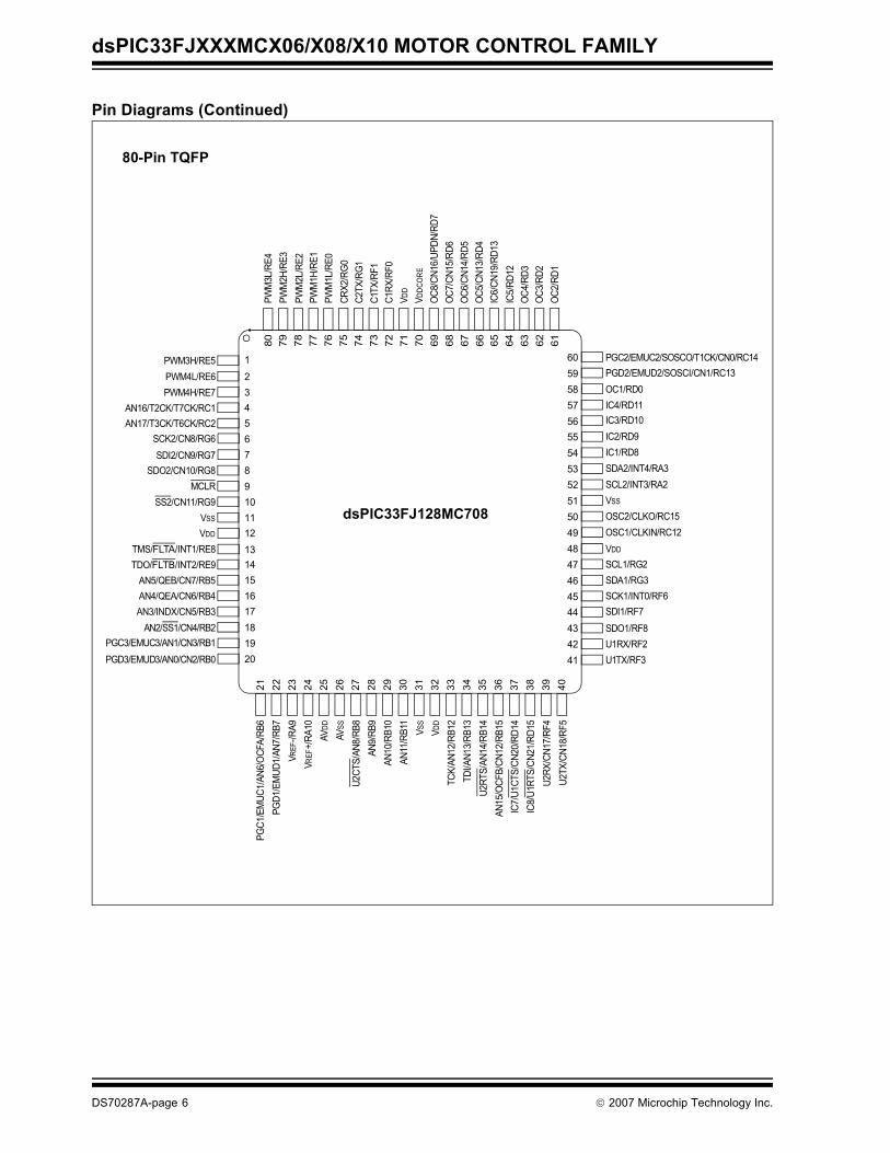
Pin Diagrams (Continued)
80-Pin TQFP
7274 73 71 70 69 68 67 66 65 64 63 62 61
20
2345678910111213141516
50494847464544
21
41
4039383736353423 24 25 26 27 28 29 30 31 32 33
171819
751
57565554535251
605958
4342
7678 777922
80
IC5/
RD12
OC4/
RD3
OC3/
RD2
OC2/
RD1
PWM
2L/R
E2PW
M1H
/RE1
PWM
1L/R
E0RG
0RG
1C1
TX/R
F1C1
RX/R
F0
PWM
3L/R
E4PW
M2H
/RE3
OC8/
CN16
/UPD
N/RD
7
OC6/
CN14
/RD5
OC1/RD0IC4/RD11
IC2/RD9IC1/RD8
IC3/RD10
VSS
OSC1/CLKIN/RC12VDD
SCL1/RG2
U1RX/RF2U1TX/RF3
PGC2/EMUC2/SOSCO/T1CK/CN0/RC14PGD2/EMUD2/SOSCI/CN1/RC13
VREF
+/RA
10VR
EF-/R
A9
AVDD
AVSS
U2CT
S/AN
8/RB
8AN
9/RB
9AN
10/R
B10
AN11
/RB1
1
VDD
U2RX
/CN1
7/RF
4IC
8/U1
RTS/
CN21
/RD1
5
U2TX
/CN1
8/RF
5
PGC1
/EM
UC1/
AN6/
OCFA
/RB6
PGD1
/EM
UD1/
AN7/
RB7
PWM4H/RE7AN16/T2CK/T7CK/RC1AN17/T3CK/T6CK/RC2
SCK2/CN8/RG6SDI2/CN9/RG7
SDO2/CN10/RG8MCLR
SS2/CN11/RG9
AN4/QEA/CN6/RB4AN3/INDX/CN5/RB3
AN2/SS1/CN4/RB2PGC3/EMUC3/AN1/CN3/RB1PGD3/EMUD3/AN0/CN2/RB0
VSS
VDD
PWM3H/RE5PWM4L/RE6
TDO/FLTB/INT2/RE9TMS/FLTA/INT1/RE8
TCK/
AN12
/RB1
2TD
I/AN1
3/RB
13U2
RTS/
AN14
/RB1
4AN
15/O
CFB/
CN12
/RB1
5
V DD
VDDC
ORE
OC5/
CN13
/RD4
IC6/
CN19
/RD1
3
SDA1/RG3
SDI1/RF7SDO1/RF8
AN5/QEB/CN7/RB5
VSS
OSC2/CLKO/RC15
OC7/
CN15
/RD6
SCK1/INT0/RF6
IC7/
U1CT
S/CN
20/R
D14
SDA2/INT4/RA3SCL2/INT3/RA2
dsPIC33FJ64MC508
© 2007 Microchip Technology Inc. DS70287A-page 5
dsPIC33FJXXXMCX06/X08/X10 MOTOR CONTROL FAMILY
Pin Diagrams (Continued)
80-Pin TQFP
7274 73 71 70 69 68 67 66 65 64 63 62 61
20
2345678910111213141516
50494847464544
21
41
4039383736353423 24 25 26 27 28 29 30 31 32 33
171819
751
57565554535251
605958
4342
7678 777922
80
IC5/
RD12
OC4/
RD3
OC3/
RD2
OC2/
RD1
PWM
2L/R
E2PW
M1H
/RE1
PWM
1L/R
E0CR
X2/R
G0
C2TX
/RG1
C1TX
/RF1
C1RX
/RF0
PWM
3L/R
E4PW
M2H
/RE3
OC8/
CN16
/UPD
N/RD
7
OC6/
CN14
/RD5
OC1/RD0IC4/RD11
IC2/RD9IC1/RD8
IC3/RD10
VSS
OSC1/CLKIN/RC12VDD
SCL1/RG2
U1RX/RF2U1TX/RF3
PGC2/EMUC2/SOSCO/T1CK/CN0/RC14PGD2/EMUD2/SOSCI/CN1/RC13
VREF
+/RA
10VR
EF-/R
A9
AVDD
AVSS
U2CT
S/AN
8/RB
8AN
9/RB
9AN
10/R
B10
AN11
/RB1
1
VDD
U2RX
/CN1
7/RF
4IC
8/U1
RTS /
CN21
/RD1
5
U2TX
/CN1
8/RF
5
PGC1
/EM
UC1/
AN6/
OCF
A/RB
6PG
D1/E
MUD
1/AN
7/RB
7
PWM4H/RE7AN16/T2CK/T7CK/RC1AN17/T3CK/T6CK/RC2
SCK2/CN8/RG6SDI2/CN9/RG7
SDO2/CN10/RG8MCLR
SS2/CN11/RG9
AN4/QEA/CN6/RB4AN3/INDX/CN5/RB3
AN2/SS1/CN4/RB2PGC3/EMUC3/AN1/CN3/RB1PGD3/EMUD3/AN0/CN2/RB0
VSS
VDD
PWM3H/RE5PWM4L/RE6
TDO/FLTB/INT2/RE9TMS/FLTA/INT1/RE8
TCK/
AN12
/RB1
2TD
I/AN1
3/RB
13U2
RTS/
AN14
/RB1
4AN
15/O
CFB/
CN12
/RB1
5
V DD
VDDC
ORE
OC5/
CN13
/RD4
IC6/
CN19
/RD1
3
SDA1/RG3
SDI1/RF7SDO1/RF8
AN5/QEB/CN7/RB5
VSS
OSC2/CLKO/RC15
OC7/
CN15
/RD6
SCK1/INT0/RF6
IC7/
U1CT
S/CN
20/R
D14
SDA2/INT4/RA3SCL2/INT3/RA2
dsPIC33FJ128MC708
DS70287A-page 6 © 2007 Microchip Technology Inc.
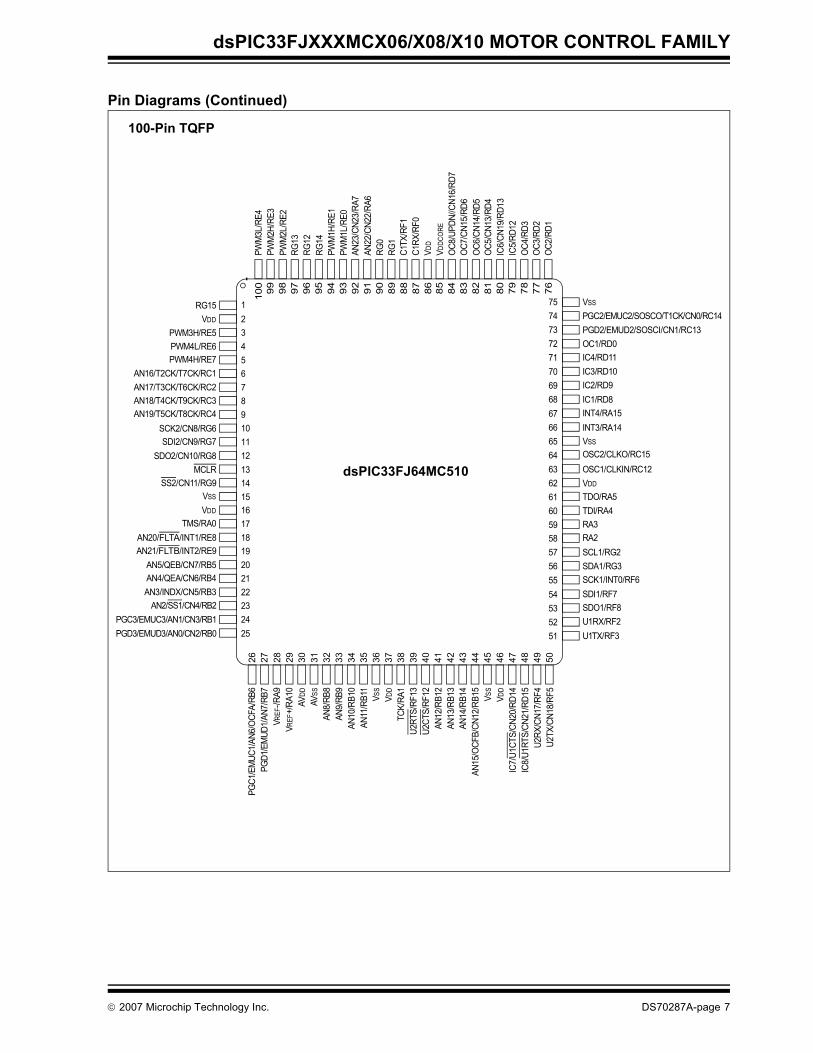
dsPIC33FJXXXMCX06/X08/X10 MOTOR CONTROL FAMILY
Pin Diagrams (Continued)
9294 93 91 90 89 88 87 86 85 84 83 82 81 80 79 78
20
2345678910111213141516
65646362616059
26
56
4544434241403928 29 30 31 32 33 34 35 36 37 38
171819
2122
951
7677
72717069686766
757473
5857
2423
25
9698 979927 46 47 48 49 50
5554535251
100
OC6
/CN1
4/RD
5O
C5/C
N13/
RD4
IC6/
CN19
/RD1
3IC
5/RD
12O
C4/R
D3O
C3/R
D2O
C2/R
D1
AN23
/CN2
3/RA
7AN
22/C
N22/
RA6
PWM
2L/R
E2RG
13RG
12RG
14PW
M1H
/RE1
PWM
1L/R
E0
RG0
PWM
3L/R
E4PW
M2H
/RE3
C1RX
/RF0
V DDC
ORE
PGD2/EMUD2/SOSCI/CN1/RC13OC1/RD0
IC3/RD10IC2/RD9IC1/RD8
IC4/RD11
RA3RA2
OSC2/CLKO/RC15OSC1/CLKIN/RC12VDD
SCL1/RG2
SCK1/INT0/RF6SDI1/RF7SDO1/RF8
SDA1/RG3
U1RX/RF2U1TX/RF3
VSS
PGC2/EMUC2/SOSCO/T1CK/CN0/RC14
VREF
+/RA
10VR
EF-/R
A9
AVDD
AVSS
AN8/
RB8
AN9/
RB9
AN10
/RB1
0AN
11/R
B11
V DD
U2CT
S/RF
12U2
RTS/
RF13
IC7/
U1CT
S /CN
20/R
D14
IC8/
U1RT
S /CN
21/R
D15
V DD
VSS
PGC1
/EM
UC1/
AN6/
OCF
A/RB
6PG
D1/E
MUD
1/AN
7/RB
7
U2TX
/CN1
8/RF
5U2
RX/C
N17/
RF4
PWM3H/RE5PWM4L/RE6PWM4H/RE7
AN16/T2CK/T7CK/RC1AN17/T3CK/T6CK/RC2AN18/T4CK/T9CK/RC3AN19/T5CK/T8CK/RC4
SCK2/CN8/RG6
VDD
TMS/RA0AN20/FLTA/INT1/RE8AN21/FLTB/INT2/RE9
AN5/QEB/CN7/RB5AN4/QEA/CN6/RB4AN3/INDX/CN5/RB3
AN2/SS1/CN4/RB2
SDI2/CN9/RG7SDO2/CN10/RG8
PGC3/EMUC3/AN1/CN3/RB1PGD3/EMUD3/AN0/CN2/RB0
RG15VDD
SS2/CN11/RG9MCLR
AN12
/RB1
2AN
13/R
B13
AN14
/RB1
4AN
15/O
CFB/
CN12
/RB1
5
RG1
C1TX
/RF1
OC8
/UPD
N//C
N16/
RD7
OC7
/CN1
5/RD
6
TDO/RA5
INT4/RA15INT3/RA14
VSS
VSS
VSS
VDD
TDI/RA4
TCK/
RA1
100-Pin TQFP
dsPIC33FJ64MC510
© 2007 Microchip Technology Inc. DS70287A-page 7
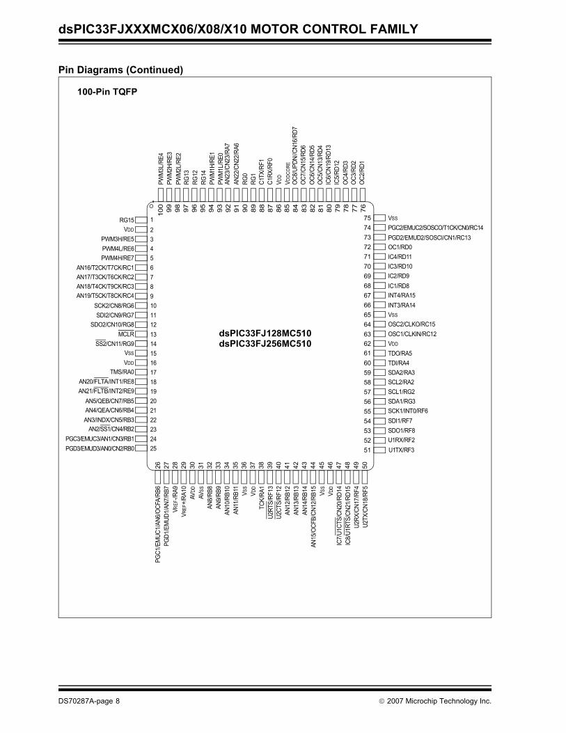
dsPIC33FJXXXMCX06/X08/X10 MOTOR CONTROL FAMILY
Pin Diagrams (Continued)
9294 93 91 90 89 88 87 86 85 84 83 82 81 80 79 78
20
2345678910111213141516
65646362616059
26
56
4544434241403928 29 30 31 32 33 34 35 36 37 38
171819
2122
95
1
7677
72717069686766
757473
5857
2423
25
9698 979927 46 47 48 49 50
5554535251
100
OC6
/CN1
4/RD
5O
C5/C
N13/
RD4
IC6/
CN19
/RD1
3IC
5/RD
12O
C4/R
D3O
C3/R
D2O
C2/R
D1
AN23
/CN2
3/RA
7AN
22/C
N22/
RA6
PWM
2L/R
E2RG
13RG
12RG
14PW
M1H
/RE1
PWM
1L/R
E0
RG0
PWM
3L/R
E4PW
M2H
/RE3
C1RX
/RF0
V DDC
ORE
PGD2/EMUD2/SOSCI/CN1/RC13OC1/RD0
IC3/RD10IC2/RD9IC1/RD8
IC4/RD11
SDA2/RA3SCL2/RA2
OSC2/CLKO/RC15OSC1/CLKIN/RC12VDD
SCL1/RG2
SCK1/INT0/RF6SDI1/RF7SDO1/RF8
SDA1/RG3
U1RX/RF2U1TX/RF3
VSS
PGC2/EMUC2/SOSCO/T1CK/CN0/RC14
VREF
+/RA
10VR
EF-/R
A9
AVDD
AVSS
AN8/
RB8
AN9/
RB9
AN10
/RB1
0AN
11/R
B11
V DD
U2CT
S/RF
12U2
RTS/
RF13
IC7/
U1CT
S /CN
20/R
D14
IC8/
U1RT
S /CN
21/R
D15
V DD
VSS
PGC1
/EM
UC1/
AN6/
OCF
A/RB
6PG
D1/E
MUD
1/AN
7/RB
7
U2TX
/CN1
8/RF
5U2
RX/C
N17/
RF4
PWM3H/RE5PWM4L/RE6PWM4H/RE7
AN16/T2CK/T7CK/RC1AN17/T3CK/T6CK/RC2AN18/T4CK/T9CK/RC3AN19/T5CK/T8CK/RC4
SCK2/CN8/RG6
VDD
TMS/RA0AN20/FLTA/INT1/RE8AN21/FLTB/INT2/RE9
AN5/QEB/CN7/RB5AN4/QEA/CN6/RB4AN3/INDX/CN5/RB3
AN2/SS1/CN4/RB2
SDI2/CN9/RG7SDO2/CN10/RG8
PGC3/EMUC3/AN1/CN3/RB1PGD3/EMUD3/AN0/CN2/RB0
RG15VDD
SS2/CN11/RG9MCLR
AN12
/RB1
2AN
13/R
B13
AN14
/RB1
4AN
15/O
CFB/
CN12
/RB1
5
RG1
C1TX
/RF1
OC8
/UPD
N//C
N16/
RD7
OC7
/CN1
5/RD
6
TDO/RA5
INT4/RA15INT3/RA14
VSS
VSS
VSS
VDD
TDI/RA4
TCK/
RA1
100-Pin TQFP
dsPIC33FJ128MC510dsPIC33FJ256MC510
DS70287A-page 8 © 2007 Microchip Technology Inc.
dsPIC33FJXXXMCX06/X08/X10 MOTOR CONTROL FAMILY
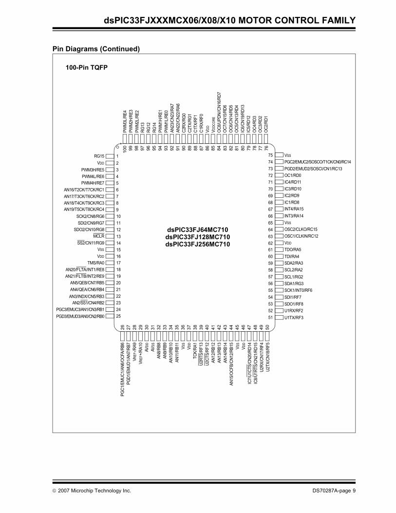
Pin Diagrams (Continued)
9294 93 91 90 89 88 87 86 85 84 83 82 81 80 79 78
20
2345678910111213141516
65646362616059
26
56
4544434241403928 29 30 31 32 33 34 35 36 37 38
171819
2122
951
7677
72717069686766
757473
5857
2423
25
9698 979927 46 47 48 49 50
5554535251
100
OC6
/CN1
4/RD
5O
C5/C
N13/
RD4
IC6/
CN19
/RD1
3IC
5/RD
12O
C4/R
D3O
C3/R
D2O
C2/R
D1
AN23
/CN2
3/RA
7AN
22/C
N22/
RA6
PWM
2L/R
E2RG
13RG
12RG
14PW
M1H
/RE1
PWM
1L/R
E0
C2RX
/RG
0
PWM
3L/R
E4PW
M2H
/RE3
C1RX
/RF0
V DDC
ORE
PGD2/EMUD2/SOSCI/CN1/RC13OC1/RD0
IC3/RD10IC2/RD9IC1/RD8
IC4/RD11
SDA2/RA3SCL2/RA2
OSC2/CLKO/RC15OSC1/CLKIN/RC12VDD
SCL1/RG2
SCK1/INT0/RF6SDI1/RF7SDO1/RF8
SDA1/RG3
U1RX/RF2U1TX/RF3
VSS
PGC2/EMUC2/SOSCO/T1CK/CN0/RC14
VREF
+/RA
10VR
EF-/R
A9
AVDD
AVSS
AN8/
RB8
AN9/
RB9
AN10
/RB1
0AN
11/R
B11
V DD
U2CT
S/RF
12U2
RTS/
RF13
IC7/
U1CT
S /CN
20/R
D14
IC8/
U1RT
S /CN
21/R
D15
V DD
VSS
PGC1
/EM
UC1/
AN6/
OCF
A/RB
6PG
D1/E
MUD
1/AN
7/RB
7
U2TX
/CN1
8/RF
5U2
RX/C
N17/
RF4
PWM3H/RE5PWM4L/RE6PWM4H/RE7
AN16/T2CK/T7CK/RC1AN17/T3CK/T6CK/RC2AN18/T4CK/T9CK/RC3AN19/T5CK/T8CK/RC4
SCK2/CN8/RG6
VDD
TMS/RA0AN20/FLTA/INT1/RE8AN21/FLTB/INT2/RE9
AN5/QEB/CN7/RB5AN4/QEA/CN6/RB4AN3/INDX/CN5/RB3
AN2/SS1/CN4/RB2
SDI2/CN9/RG7SDO2/CN10/RG8
PGC3/EMUC3/AN1/CN3/RB1PGD3/EMUD3/AN0/CN2/RB0
RG15VDD
SS2/CN11/RG9MCLR
AN12
/RB1
2AN
13/R
B13
AN14
/RB1
4AN
15/O
CFB/
CN12
/RB1
5
C2TX
/RG1
C1TX
/RF1
OC8
/UPD
N//C
N16/
RD7
OC7
/CN1
5/RD
6
TDO/RA5
INT4/RA15INT3/RA14
VSS
VSS
VSS
VDD
TDI/RA4
TCK/
RA1
100-Pin TQFP
dsPIC33FJ64MC710dsPIC33FJ128MC710dsPIC33FJ256MC710
© 2007 Microchip Technology Inc. DS70287A-page 9
dsPIC33FJXXXMCX06/X08/X10 MOTOR CONTROL FAMILY
Table of ContentsdsPIC33F Product Families ................................................................................................................................................................... 31.0 Device Overview ........................................................................................................................................................................ 132.0 CPU............................................................................................................................................................................................ 173.0 Memory Organization ................................................................................................................................................................. 294.0 Flash Program Memory.............................................................................................................................................................. 675.0 Resets ....................................................................................................................................................................................... 736.0 Interrupt Controller ..................................................................................................................................................................... 797.0 Direct Memory Access (DMA) .................................................................................................................................................. 1278.0 Oscillator Configuration ............................................................................................................................................................ 1379.0 Power-Saving Features............................................................................................................................................................ 14510.0 I/O Ports ................................................................................................................................................................................... 14711.0 Timer1 ...................................................................................................................................................................................... 14912.0 Timer2/3, Timer4/5, Timer6/7 and Timer8/9 ............................................................................................................................ 15113.0 Input Capture............................................................................................................................................................................ 15714.0 Output Compare....................................................................................................................................................................... 15915.0 Motor Control PWM Module ..................................................................................................................................................... 16316.0 Quadrature Encoder Interface (QEI) Module ........................................................................................................................... 18517.0 Serial Peripheral Interface (SPI)............................................................................................................................................... 19318.0 Inter-Integrated Circuit (I2C) ..................................................................................................................................................... 20119.0 Universal Asynchronous Receiver Transmitter (UART) ........................................................................................................... 21120.0 Enhanced CAN Module............................................................................................................................................................ 21921.0 10-bit/12-bit Analog-to-Digital Converter (ADC) ....................................................................................................................... 24922.0 Special Features ...................................................................................................................................................................... 26323.0 Instruction Set Summary .......................................................................................................................................................... 27124.0 Development Support............................................................................................................................................................... 27925.0 Electrical Characteristics .......................................................................................................................................................... 28326.0 Packaging Information.............................................................................................................................................................. 323Appendix A: Differences Between “PS” (Prototype Sample) Devices and Final Production Devices................................................ 329Appendix B: Revision History............................................................................................................................................................. 330Index ................................................................................................................................................................................................. 331The Microchip Web Site ..................................................................................................................................................................... 337Customer Change Notification Service .............................................................................................................................................. 337Customer Support .............................................................................................................................................................................. 337Reader Response .............................................................................................................................................................................. 338Product Identification System............................................................................................................................................................. 339
DS70287A-page 10 © 2007 Microchip Technology Inc.
dsPIC33FJXXXMCX06/X08/X10 MOTOR CONTROL FAMILY
TO OUR VALUED CUSTOMERSIt is our intention to provide our valued customers with the best documentation possible to ensure successful use of your Microchipproducts. To this end, we will continue to improve our publications to better suit your needs. Our publications will be refined andenhanced as new volumes and updates are introduced. If you have any questions or comments regarding this publication, please contact the Marketing Communications Department viaE-mail at [email protected] or fax the Reader Response Form in the back of this data sheet to (480) 792-4150. Wewelcome your feedback.
Most Current Data SheetTo obtain the most up-to-date version of this data sheet, please register at our Worldwide Web site at:
http://www.microchip.comYou can determine the version of a data sheet by examining its literature number found on the bottom outside corner of any page.The last character of the literature number is the version number, (e.g., DS30000A is version A of document DS30000).
ErrataAn errata sheet, describing minor operational differences from the data sheet and recommended workarounds, may exist for currentdevices. As device/documentation issues become known to us, we will publish an errata sheet. The errata will specify the revisionof silicon and revision of document to which it applies.To determine if an errata sheet exists for a particular device, please check with one of the following:• Microchip’s Worldwide Web site; http://www.microchip.com• Your local Microchip sales office (see last page)When contacting a sales office, please specify which device, revision of silicon and data sheet (include literature number) you areusing.
Customer Notification SystemRegister on our web site at www.microchip.com to receive the most current information on all of our products.
© 2007 Microchip Technology Inc. DS70287A-page 11

dsPIC33FJXXXMCX06/X08/X10 MOTOR CONTROL FAMILY
NOTES:
DS70287A-page 12 © 2007 Microchip Technology Inc.
dsPIC33FJXXXMCX06/X08/X10 MOTOR CONTROL FAMILY
1.0 DEVICE OVERVIEW
This document contains device specific information forthe following devices:
• dsPIC33FJ64MC506• dsPIC33FJ64MC508• dsPIC33FJ64MC510• dsPIC33FJ64MC706• dsPIC33FJ64MC710• dsPIC33FJ128MC506• dsPIC33FJ128MC510• dsPIC33FJ128MC706• dsPIC33FJ128MC708• dsPIC33FJ128MC710• dsPIC33FJ256MC510• dsPIC33FJ256MC710
The dsPIC33FJXXXMCX06/X08/X10 Motor ControlFamily includes devices with a wide range of pin counts(64, 80 and 100), different program memory sizes (64Kbytes, 128 Kbytes and 256 Kbytes) and different RAMsizes (8 Kbytes, 16 Kbytes and 30 Kbytes).
These features make this family suitable for a wide vari-ety of high-performance digital signal control applica-tions. The devices are pin compatible with the PIC24Hfamily of devices, and also share a very high degree ofcompatibility with the dsPIC30F family devices. Thisallows easy migration between device families as may benecessitated by the specific functionality, computationalresource and system cost requirements of theapplication.
The dsPIC33FJXXXMCX06/X08/X10 Motor ControlFamily of devices employ a powerful 16-bitarchitecture that seamlessly integrates the controlfeatures of a Microcontroller (MCU) with thecomputational capabilities of a Digital Signal Processor(DSP). The resulting functionality is ideal forapplications that rely on high-speed, repetitivecomputations, as well as control.
The DSP engine, dual 40-bit accumulators, hardwaresupport for division operations, barrel shifter, 17 x 17multiplier, a large array of 16-bit working registers anda wide variety of data addressing modes, together,provide the dsPIC33FJXXXMCX06/X08/X10 MotorControl Family Central Processing Unit (CPU) withextensive mathematical processing capability. Flexibleand deterministic interrupt handling, coupled with apowerful array of peripherals, renders thedsPIC33FJXXXMCX06/X08/X10 Motor Control Familydevices suitable for control applications. Further, DirectMemory Access (DMA) enables overhead-free transferof data between several peripherals and a dedicatedDMA RAM. Reliable, field programmable Flashprogram memory ensures scalability of applicationsthat use dsPIC33FJXXXMCX06/X08/X10 MotorControl Family devices.
Note: This data sheet summarizes the featuresof this groupof dsPIC33FJXXXMCX06/X08/X10 MotorControl Family devices. It is not intendedto be a comprehensive reference source.To complement the information in this datasheet, refer to the “dsPIC33F Family Ref-erence Manual”. Refer to the Microchipweb site (www.microchip.com) for the lat-est dsPIC33F family reference manualchapters.
© 2007 Microchip Technology Inc. DS70287A-page 13
dsPIC33FJXXXMCX06/X08/X10 MOTOR CONTROL FAMILY
FIGURE 1-1: dsPIC33FJXXXMCX06/X08/X10 MOTOR CONTROL FAMILY GENERAL BLOCK DIAGRAM
16
OSC1/CLKIOSC2/CLKO
VDD, VSS
TimingGeneration
MCLR
Power-upTimer
OscillatorStart-up Timer
Power-onReset
WatchdogTimer
Brown-outReset
Precision
ReferenceBand Gap
FRC/LPRCOscillators
RegulatorVoltage
VDDCORE/VCAP
UART1,2
ECAN1,2PWM
IC1-8OC/
SPI1,2 I2C1,2
QEI
PORTA
Note: Not all pins or features are implemented on all device pinout configurations. See pinout diagrams for the specific pinsand features present on each device.
PWM1-8CN1-23
InstructionDecode &
Control
PCH PCL
16
Program Counter
16-bit ALU
23
23
24
23
Instruction Reg
PCU
16 x 16W Register Array
ROM Latch
16
EA MUX
16
16
8
InterruptController
PSV & TableData AccessControl Block
StackControl
Logic
LoopControlLogic
Data Latch
AddressLatch
Address Latch
Program Memory
Data LatchAddress Bus
L
itera
l Dat
a 16 16
16
16
Data Latch
AddressLatch
16
X RAM Y RAM
16
Y Data Bus
X Data Bus
DSP Engine
Divide Support
16
DMARAM
DMA
Controller
Control Signals to Various Blocks
ADC1,2Timers
PORTB
PORTC
PORTD
PORTE
PORTF
PORTG
Address Generator Units
1-9
DS70287A-page 14 © 2007 Microchip Technology Inc.
dsPIC33FJXXXMCX06/X08/X10 MOTOR CONTROL FAMILY
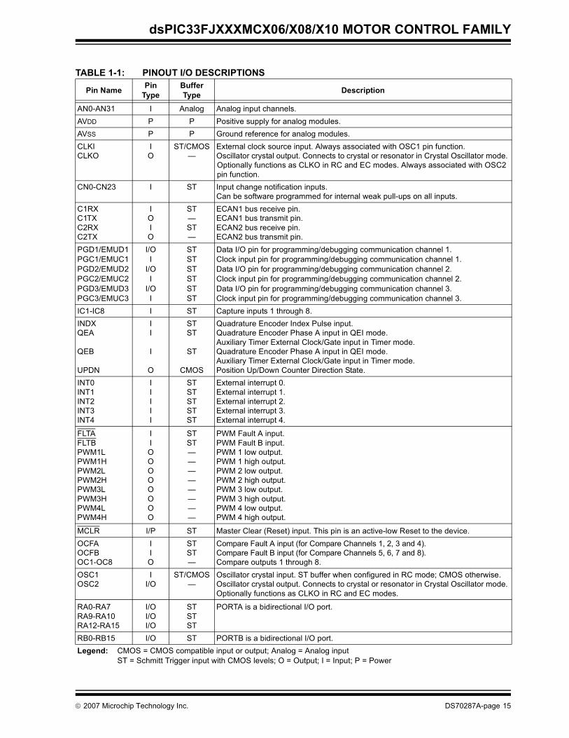
TABLE 1-1: PINOUT I/O DESCRIPTIONS
Pin Name PinType
BufferType Description
AN0-AN31 I Analog Analog input channels. AVDD P P Positive supply for analog modules.AVSS P P Ground reference for analog modules.CLKICLKO
IO
ST/CMOS—
External clock source input. Always associated with OSC1 pin function.Oscillator crystal output. Connects to crystal or resonator in Crystal Oscillator mode. Optionally functions as CLKO in RC and EC modes. Always associated with OSC2 pin function.
CN0-CN23 I ST Input change notification inputs.Can be software programmed for internal weak pull-ups on all inputs.
C1RXC1TXC2RXC2TX
IOIO
ST—ST—
ECAN1 bus receive pin.ECAN1 bus transmit pin.ECAN2 bus receive pin.ECAN2 bus transmit pin.
PGD1/EMUD1PGC1/EMUC1PGD2/EMUD2PGC2/EMUC2PGD3/EMUD3PGC3/EMUC3
I/OI
I/OI
I/OI
STSTSTSTSTST
Data I/O pin for programming/debugging communication channel 1.Clock input pin for programming/debugging communication channel 1.Data I/O pin for programming/debugging communication channel 2.Clock input pin for programming/debugging communication channel 2.Data I/O pin for programming/debugging communication channel 3.Clock input pin for programming/debugging communication channel 3.
IC1-IC8 I ST Capture inputs 1 through 8.INDXQEA
QEB
UPDN
II
I
O
STST
ST
CMOS
Quadrature Encoder Index Pulse input.Quadrature Encoder Phase A input in QEI mode. Auxiliary Timer External Clock/Gate input in Timer mode.Quadrature Encoder Phase A input in QEI mode. Auxiliary Timer External Clock/Gate input in Timer mode.Position Up/Down Counter Direction State.
INT0INT1INT2INT3INT4
IIIII
STSTSTSTST
External interrupt 0.External interrupt 1.External interrupt 2.External interrupt 3.External interrupt 4.
FLTAFLTBPWM1LPWM1HPWM2LPWM2HPWM3LPWM3HPWM4LPWM4H
IIOOOOOOOO
STST————————
PWM Fault A input.PWM Fault B input.PWM 1 low output. PWM 1 high output.PWM 2 low output.PWM 2 high output.PWM 3 low output.PWM 3 high output.PWM 4 low output.PWM 4 high output.
MCLR I/P ST Master Clear (Reset) input. This pin is an active-low Reset to the device.OCFAOCFBOC1-OC8
IIO
STST—
Compare Fault A input (for Compare Channels 1, 2, 3 and 4).Compare Fault B input (for Compare Channels 5, 6, 7 and 8).Compare outputs 1 through 8.
OSC1OSC2
II/O
ST/CMOS—
Oscillator crystal input. ST buffer when configured in RC mode; CMOS otherwise.Oscillator crystal output. Connects to crystal or resonator in Crystal Oscillator mode. Optionally functions as CLKO in RC and EC modes.
RA0-RA7RA9-RA10RA12-RA15
I/OI/OI/O
STSTST
PORTA is a bidirectional I/O port.
RB0-RB15 I/O ST PORTB is a bidirectional I/O port.Legend: CMOS = CMOS compatible input or output; Analog = Analog input
ST = Schmitt Trigger input with CMOS levels; O = Output; I = Input; P = Power
© 2007 Microchip Technology Inc. DS70287A-page 15
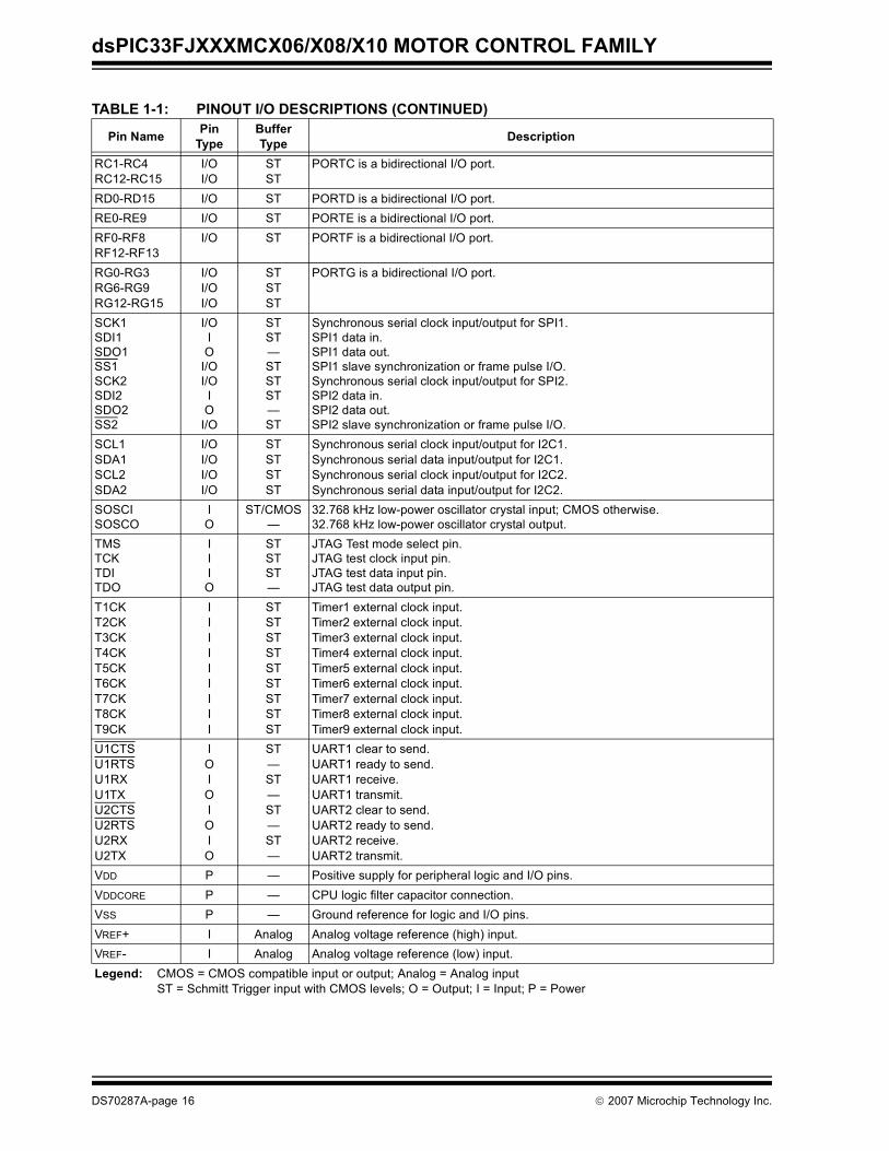
dsPIC33FJXXXMCX06/X08/X10 MOTOR CONTROL FAMILY
RC1-RC4RC12-RC15
I/OI/O
STST
PORTC is a bidirectional I/O port.
RD0-RD15 I/O ST PORTD is a bidirectional I/O port.RE0-RE9 I/O ST PORTE is a bidirectional I/O port.RF0-RF8 RF12-RF13
I/O ST PORTF is a bidirectional I/O port.
RG0-RG3RG6-RG9RG12-RG15
I/OI/OI/O
STSTST
PORTG is a bidirectional I/O port.
SCK1SDI1SDO1SS1SCK2SDI2SDO2SS2
I/OIO
I/OI/OIO
I/O
STST—STSTST—ST
Synchronous serial clock input/output for SPI1.SPI1 data in.SPI1 data out.SPI1 slave synchronization or frame pulse I/O.Synchronous serial clock input/output for SPI2.SPI2 data in.SPI2 data out.SPI2 slave synchronization or frame pulse I/O.
SCL1SDA1SCL2SDA2
I/OI/OI/OI/O
STSTSTST
Synchronous serial clock input/output for I2C1.Synchronous serial data input/output for I2C1.Synchronous serial clock input/output for I2C2.Synchronous serial data input/output for I2C2.
SOSCISOSCO
IO
ST/CMOS—
32.768 kHz low-power oscillator crystal input; CMOS otherwise.32.768 kHz low-power oscillator crystal output.
TMSTCKTDITDO
IIIO
STSTST—
JTAG Test mode select pin.JTAG test clock input pin.JTAG test data input pin.JTAG test data output pin.
T1CKT2CKT3CKT4CKT5CKT6CKT7CKT8CKT9CK
IIIIIIIII
STSTSTSTSTSTSTSTST
Timer1 external clock input.Timer2 external clock input.Timer3 external clock input.Timer4 external clock input.Timer5 external clock input.Timer6 external clock input.Timer7 external clock input.Timer8 external clock input.Timer9 external clock input.
U1CTSU1RTSU1RXU1TXU2CTSU2RTSU2RXU2TX
IOIOIOIO
ST—ST—ST—ST—
UART1 clear to send.UART1 ready to send.UART1 receive.UART1 transmit.UART2 clear to send.UART2 ready to send.UART2 receive.UART2 transmit.
VDD P — Positive supply for peripheral logic and I/O pins.VDDCORE P — CPU logic filter capacitor connection.VSS P — Ground reference for logic and I/O pins.VREF+ I Analog Analog voltage reference (high) input.VREF- I Analog Analog voltage reference (low) input.
TABLE 1-1: PINOUT I/O DESCRIPTIONS (CONTINUED)
Pin Name PinType
BufferType Description
Legend: CMOS = CMOS compatible input or output; Analog = Analog inputST = Schmitt Trigger input with CMOS levels; O = Output; I = Input; P = Power
DS70287A-page 16 © 2007 Microchip Technology Inc.
dsPIC33FJXXXMCX06/X08/X10 MOTOR CONTROL FAMILY
2.0 CPU
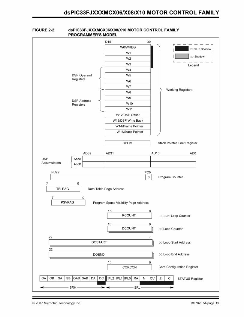
The dsPIC33FJXXXMCX06/X08/X10 Motor ControlFamily CPU module has a 16-bit (data) modified Har-vard architecture with an enhanced instruction set,including significant support for DSP. The CPU has a24-bit instruction word with a variable length opcodefield. The Program Counter (PC) is 23 bits wide andaddresses up to 4M x 24 bits of user program memoryspace. The actual amount of program memory imple-mented varies by device. A single-cycle instructionprefetch mechanism is used to help maintain through-put and provides predictable execution. All instructionsexecute in a single cycle, with the exception of instruc-tions that change the program flow, the double wordmove (MOV.D) instruction and the table instructions.Overhead-free program loop constructs are supportedusing the DO and REPEAT instructions, both of whichare interruptible at any point.
The dsPIC33FJXXXMCX06/X08/X10 Motor ControlFamily devices have sixteen 16-bit working registers inthe programmer’s model. Each of the working registerscan serve as a data, address or address offset register.The 16th working register (W15) operates as a soft-ware Stack Pointer (SP) for interrupts and calls.
The dsPIC33FJXXXMCX06/X08/X10 Motor ControlFamily instruction set has two classes of instructions:MCU and DSP. These two instruction classes areseamlessly integrated into a single CPU. The instruc-tion set includes many addressing modes and isdesigned for optimum C compiler efficiency. For mostinstructions, the dsPIC33FJXXXMCX06/X08/X10Motor Control Family is capable of executing a data (orprogram data) memory read, a working register (data)read, a data memory write and a program (instruction)memory read per instruction cycle. As a result, threeparameter instructions can be supported, allowing A +B = C operations to be executed in a single cycle.
A block diagram of the CPU is shown in Figure 2-1, andthe programmer’s model for thedsPIC33FJXXXMCX06/X08/X10 Motor Control Familyis shown in Figure 2-2.
2.1 Data Addressing OverviewThe data space can be addressed as 32K words or64 Kbytes and is split into two blocks referred to as Xand Y data memory. Each memory block has its ownindependent Address Generation Unit (AGU). TheMCU class of instructions operates solely through theX memory AGU, which accesses the entire memorymap as one linear data space. Certain DSP instructionsoperate through the X and Y AGUs to support dualoperand reads, which splits the data address spaceinto two parts. The X and Y data space boundary isdevice-specific.
Overhead-free circular buffers (Modulo Addressingmode) are supported in both X and Y address spaces.The Modulo Addressing removes the software bound-ary checking overhead for DSP algorithms. Further-more, the X AGU circular addressing can be used withany of the MCU class of instructions. The X AGU alsosupports Bit-Reversed Addressing to greatly simplifyinput or output data reordering for radix-2 FFT algo-rithms.
The upper 32 Kbytes of the data space memory mapcan optionally be mapped into program space at any16K program word boundary defined by the 8-bit Pro-gram Space Visibility Page (PSVPAG) register. Theprogram to data space mapping feature lets anyinstruction access program space as if it were dataspace.
The data space also includes 2 Kbytes of DMA RAM,which is primarily used for DMA data transfers but maybe used as general purpose RAM.
2.2 DSP Engine OverviewThe DSP engine features a high-speed, 17-bit by 17-bitmultiplier, a 40-bit ALU, two 40-bit saturating accumu-lators and a 40-bit bidirectional barrel shifter. The barrelshifter is capable of shifting a 40-bit value up to 16 bitsright or left in a single cycle. The DSP instructions oper-ate seamlessly with all other instructions and havebeen designed for optimal real-time performance. TheMAC instruction and other associated instructions canconcurrently fetch two data operands from memorywhile multiplying two W registers and accumulating andoptionally saturating the result in the same cycle. Thisinstruction functionality requires that the RAM memorydata space be split for these instructions and linear forall others. Data space partitioning is achieved in atransparent and flexible manner through dedicatingcertain working registers to each address space.
Note: This data sheet summarizes the featuresof this groupof dsPIC33FJXXXMCX06/X08/X10 MotorControl Family devices. It is not intendedto be a comprehensive reference source.To complement the information in this datasheet, refer to the “dsPIC33F FamilyReference Manual”. Refer to theMicrochip web site (www.microchip.com)for the latest dsPIC33F family referencemanual chapters.
© 2007 Microchip Technology Inc. DS70287A-page 17
dsPIC33FJXXXMCX06/X08/X10 MOTOR CONTROL FAMILY
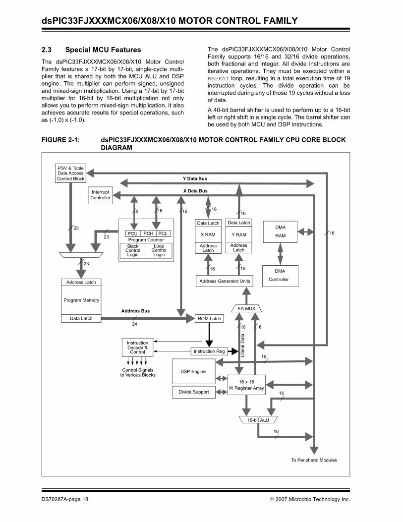
2.3 Special MCU FeaturesThe dsPIC33FJXXXMCX06/X08/X10 Motor ControlFamily features a 17-bit by 17-bit, single-cycle multi-plier that is shared by both the MCU ALU and DSPengine. The multiplier can perform signed, unsignedand mixed-sign multiplication. Using a 17-bit by 17-bitmultiplier for 16-bit by 16-bit multiplication not onlyallows you to perform mixed-sign multiplication, it alsoachieves accurate results for special operations, suchas (-1.0) x (-1.0).
The dsPIC33FJXXXMCX06/X08/X10 Motor ControlFamily supports 16/16 and 32/16 divide operations,both fractional and integer. All divide instructions areiterative operations. They must be executed within aREPEAT loop, resulting in a total execution time of 19instruction cycles. The divide operation can beinterrupted during any of those 19 cycles without a lossof data.
A 40-bit barrel shifter is used to perform up to a 16-bitleft or right shift in a single cycle. The barrel shifter canbe used by both MCU and DSP instructions.
FIGURE 2-1: dsPIC33FJXXXMCX06/X08/X10 MOTOR CONTROL FAMILY CPU CORE BLOCK DIAGRAM
InstructionDecode &
Control
PCH PCLProgram Counter
16-bit ALU
24
23
Instruction Reg
PCU
16 x 16W Register Array
ROM Latch
EA MUX
InterruptController
StackControlLogic
LoopControlLogic
Data Latch
AddressLatch
Control Signalsto Various Blocks
Address Bus
L
itera
l Dat
a
16 16
16
To Peripheral Modules
Data Latch
AddressLatch
16
X RAM Y RAM
Address Generator Units
16
Y Data Bus
X Data Bus
DMA
Controller
DMA
RAM
DSP Engine
Divide Support
16
16
23
23
168
PSV & TableData AccessControl Block
16
16
16
16
Program Memory
Data Latch
Address Latch
DS70287A-page 18 © 2007 Microchip Technology Inc.
dsPIC33FJXXXMCX06/X08/X10 MOTOR CONTROL FAMILY
FIGURE 2-2: dsPIC33FJXXXMCX06/X08/X10 MOTOR CONTROL FAMILY PROGRAMMER’S MODEL
PC22 PC0
7 0
D0D15
Program Counter
Data Table Page Address
STATUS Register
Working Registers
DSP OperandRegisters
W1
W2
W3
W4
W5
W6
W7
W8
W9
W10
W11
W12/DSP Offset
W13/DSP Write Back
W14/Frame Pointer
W15/Stack Pointer
DSP AddressRegisters
AD39 AD0AD31
DSPAccumulators
AccA
AccB
7 0Program Space Visibility Page Address
Z
0
OA OB SA SB
RCOUNT15 0
REPEAT Loop Counter
DCOUNT15 0
DO Loop Counter
DOSTART 22 0
DO Loop Start Address
IPL2 IPL1
SPLIM Stack Pointer Limit Register
AD15
SRL
PUSH.S Shadow
DO Shadow
OAB SAB
15 0Core Configuration Register
Legend
CORCON
DA DC RA N
TBLPAG
PSVPAG
IPL0 OV
W0/WREG
SRH
DO Loop End AddressDOEND 22
C
© 2007 Microchip Technology Inc. DS70287A-page 19

dsPIC33FJXXXMCX06/X08/X10 MOTOR CONTROL FAMILY
2.4 CPU Control Registers
REGISTER 2-1: SR: CPU STATUS REGISTER
R-0 R-0 R/C-0 R/C-0 R-0 R/C-0 R -0 R/W-0OA OB SA(1) SB(1) OAB SAB DA DC
bit 15 bit 8
R/W-0(2) R/W-0(3) R/W-0(3) R-0 R/W-0 R/W-0 R/W-0 R/W-0IPL<2:0>(2) RA N OV Z C
bit 7 bit 0
Legend:C = Clear only bit R = Readable bit U = Unimplemented bit, read as ‘0’S = Set only bit W = Writable bit -n = Value at POR‘1’ = Bit is set ‘0’ = Bit is cleared x = Bit is unknown
bit 15 OA: Accumulator A Overflow Status bit1 = Accumulator A overflowed0 = Accumulator A has not overflowed
bit 14 OB: Accumulator B Overflow Status bit1 = Accumulator B overflowed0 = Accumulator B has not overflowed
bit 13 SA: Accumulator A Saturation ‘Sticky’ Status bit(1)
1 = Accumulator A is saturated or has been saturated at some time0 = Accumulator A is not saturated
bit 12 SB: Accumulator B Saturation ‘Sticky’ Status bit(1)
1 = Accumulator B is saturated or has been saturated at some time0 = Accumulator B is not saturated
bit 11 OAB: OA || OB Combined Accumulator Overflow Status bit1 = Accumulators A or B have overflowed0 = Neither Accumulators A or B have overflowed
bit 10 SAB: SA || SB Combined Accumulator ‘Sticky’ Status bit1 = Accumulators A or B are saturated or have been saturated at some time in the past0 = Neither Accumulator A or B are saturated
Note: This bit may be read or cleared (not set). Clearing this bit will clear SA and SB.bit 9 DA: DO Loop Active bit
1 = DO loop in progress0 = DO loop not in progress
bit 8 DC: MCU ALU Half Carry/Borrow bit1 = A carry-out from the 4th low-order bit (for byte sized data) or 8th low-order bit (for word sized data)
of the result occurred0 = No carry-out from the 4th low-order bit (for byte sized data) or 8th low-order bit (for word sized
data) of the result occurred
Note 1: This bit may be read or cleared (not set).2: The IPL<2:0> bits are concatenated with the IPL<3> bit (CORCON<3>) to form the CPU Interrupt Priority
Level. The value in parentheses indicates the IPL if IPL<3> = 1. User interrupts are disabled when IPL<3> = 1.
3: The IPL<2:0> Status bits are read only when NSTDIS = 1 (INTCON1<15>).
DS70287A-page 20 © 2007 Microchip Technology Inc.
dsPIC33FJXXXMCX06/X08/X10 MOTOR CONTROL FAMILY
bit 7-5 IPL<2:0>: CPU Interrupt Priority Level Status bits(2)
111 = CPU Interrupt Priority Level is 7 (15), user interrupts disabled110 = CPU Interrupt Priority Level is 6 (14)101 = CPU Interrupt Priority Level is 5 (13)100 = CPU Interrupt Priority Level is 4 (12)011 = CPU Interrupt Priority Level is 3 (11)010 = CPU Interrupt Priority Level is 2 (10)001 = CPU Interrupt Priority Level is 1 (9)000 = CPU Interrupt Priority Level is 0 (8)
bit 4 RA: REPEAT Loop Active bit1 = REPEAT loop in progress0 = REPEAT loop not in progress
bit 3 N: MCU ALU Negative bit1 = Result was negative0 = Result was non-negative (zero or positive)
bit 2 OV: MCU ALU Overflow bitThis bit is used for signed arithmetic (2’s complement). It indicates an overflow of the magnitude thatcauses the sign bit to change state. 1 = Overflow occurred for signed arithmetic (in this arithmetic operation)0 = No overflow occurred
bit 1 Z: MCU ALU Zero bit1 = An operation which affects the Z bit has set it at some time in the past0 = The most recent operation which affects the Z bit has cleared it (i.e., a non-zero result)
bit 0 C: MCU ALU Carry/Borrow bit1 = A carry-out from the Most Significant bit of the result occurred0 = No carry-out from the Most Significant bit of the result occurred
REGISTER 2-1: SR: CPU STATUS REGISTER (CONTINUED)
Note 1: This bit may be read or cleared (not set).2: The IPL<2:0> bits are concatenated with the IPL<3> bit (CORCON<3>) to form the CPU Interrupt Priority
Level. The value in parentheses indicates the IPL if IPL<3> = 1. User interrupts are disabled when IPL<3> = 1.
3: The IPL<2:0> Status bits are read only when NSTDIS = 1 (INTCON1<15>).
© 2007 Microchip Technology Inc. DS70287A-page 21
dsPIC33FJXXXMCX06/X08/X10 MOTOR CONTROL FAMILY
REGISTER 2-2: CORCON: CORE CONTROL REGISTER
U-0 U-0 U-0 R/W-0 R/W-0 R-0 R-0 R-0— — — US EDT(1) DL<2:0>
bit 15 bit 8
R/W-0 R/W-0 R/W-1 R/W-0 R/C-0 R/W-0 R/W-0 R/W-0SATA SATB SATDW ACCSAT IPL3(2) PSV RND IF
bit 7 bit 0
Legend: C = Clear only bitR = Readable bit W = Writable bit -n = Value at POR ‘1’ = Bit is set0’ = Bit is cleared ‘x = Bit is unknown U = Unimplemented bit, read as ‘0’
bit 15-13 Unimplemented: Read as ‘0’bit 12 US: DSP Multiply Unsigned/Signed Control bit
1 = DSP engine multiplies are unsigned 0 = DSP engine multiplies are signed
bit 11 EDT: Early DO Loop Termination Control bit(1)
1 = Terminate executing DO loop at end of current loop iteration0 = No effect
bit 10-8 DL<2:0>: DO Loop Nesting Level Status bits111 = 7 DO loops active•••001 = 1 DO loop active000 = 0 DO loops active
bit 7 SATA: AccA Saturation Enable bit1 = Accumulator A saturation enabled0 = Accumulator A saturation disabled
bit 6 SATB: AccB Saturation Enable bit1 = Accumulator B saturation enabled0 = Accumulator B saturation disabled
bit 5 SATDW: Data Space Write from DSP Engine Saturation Enable bit1 = Data space write saturation enabled0 = Data space write saturation disabled
bit 4 ACCSAT: Accumulator Saturation Mode Select bit1 = 9.31 saturation (super saturation)0 = 1.31 saturation (normal saturation)
bit 3 IPL3: CPU Interrupt Priority Level Status bit 3(2)
1 = CPU interrupt priority level is greater than 70 = CPU interrupt priority level is 7 or less
bit 2 PSV: Program Space Visibility in Data Space Enable bit1 = Program space visible in data space0 = Program space not visible in data space
bit 1 RND: Rounding Mode Select bit1 = Biased (conventional) rounding enabled0 = Unbiased (convergent) rounding enabled
bit 0 IF: Integer or Fractional Multiplier Mode Select bit1 = Integer mode enabled for DSP multiply ops0 = Fractional mode enabled for DSP multiply ops
Note 1: This bit will always read as ‘0’.2: The IPL3 bit is concatenated with the IPL<2:0> bits (SR<7:5>) to form the CPU interrupt priority level.
DS70287A-page 22 © 2007 Microchip Technology Inc.
dsPIC33FJXXXMCX06/X08/X10 MOTOR CONTROL FAMILY
2.5 Arithmetic Logic Unit (ALU)The dsPIC33FJXXXMCX06/X08/X10 Motor ControlFamily ALU is 16 bits wide and is capable of addition,subtraction, bit shifts and logic operations. Unless oth-erwise mentioned, arithmetic operations are 2’s com-plement in nature. Depending on the operation, theALU may affect the values of the Carry (C), Zero (Z),Negative (N), Overflow (OV) and Digit Carry (DC) Sta-tus bits in the SR register. The C and DC Status bitsoperate as Borrow and Digit Borrow bits, respectively,for subtraction operations.
The ALU can perform 8-bit or 16-bit operations,depending on the mode of the instruction that is used.Data for the ALU operation can come from the W reg-ister array or data memory, depending on the address-ing mode of the instruction. Likewise, output data fromthe ALU can be written to the W register array or a datamemory location.
Refer to the “dsPIC30F/33F Programmer’s ReferenceManual” (DS70157) for information on the SR bitsaffected by each instruction.
The dsPIC33FJXXXMCX06/X08/X10 Motor ControlFamily CPU incorporates hardware support for bothmultiplication and division. This includes a dedicatedhardware multiplier and support hardware for16-bit-divisor division.
2.5.1 MULTIPLIERUsing the high-speed 17-bit x 17-bit multiplier of theDSP engine, the ALU supports unsigned, signed ormixed-sign operation in several MCU multiplicationmodes:
1. 16-bit x 16-bit signed2. 16-bit x 16-bit unsigned3. 16-bit signed x 5-bit (literal) unsigned4. 16-bit unsigned x 16-bit unsigned5. 16-bit unsigned x 5-bit (literal) unsigned6. 16-bit unsigned x 16-bit signed7. 8-bit unsigned x 8-bit unsigned
2.5.2 DIVIDERThe divide block supports 32-bit/16-bit and 16-bit/16-bitsigned and unsigned integer divide operations with thefollowing data sizes:
1. 32-bit signed/16-bit signed divide2. 32-bit unsigned/16-bit unsigned divide3. 16-bit signed/16-bit signed divide4. 16-bit unsigned/16-bit unsigned divide
The quotient for all divide instructions ends up in W0and the remainder in W1. 16-bit signed and unsignedDIV instructions can specify any W register for both the16-bit divisor (Wn) and any W register (aligned) pair(W(m + 1):Wm) for the 32-bit dividend. The divide algo-rithm takes one cycle per bit of divisor, so both32-bit/16-bit and 16-bit/16-bit instructions take thesame number of cycles to execute.
2.6 DSP EngineThe DSP engine consists of a high-speed, 17-bit x17-bit multiplier, a barrel shifter and a 40-bitadder/subtracter (with two target accumulators, roundand saturation logic).
The dsPIC33FJXXXMCX06/X08/X10 Motor ControlFamily is a single-cycle, instruction flow architecture;therefore, concurrent operation of the DSP engine withMCU instruction flow is not possible. However, someMCU ALU and DSP engine resources may be usedconcurrently by the same instruction (e.g., ED, EDAC).
The DSP engine also has the capability to performinherent accumulator-to-accumulator operations whichrequire no additional data. These instructions are ADD,SUB and NEG.
The DSP engine has various options selected throughvarious bits in the CPU Core Control register(CORCON), as listed below:
1. Fractional or integer DSP multiply (IF)2. Signed or unsigned DSP multiply (US)3. Conventional or convergent rounding (RND)4. Automatic saturation on/off for AccA (SATA)5. Automatic saturation on/off for AccB (SATB)6. Automatic saturation on/off for writes to data
memory (SATDW)7. Accumulator Saturation mode selection (ACCSAT)
Table 2-1 provides a summary of DSP instructions. Ablock diagram of the DSP engine is shown inFigure 2-3.
TABLE 2-1: DSP INSTRUCTIONS SUMMARY
Instruction Algebraic Operation
ACC Write Back
CLR A = 0 YesED A = (x – y)2 NoEDAC A = A + (x – y)2 NoMAC A = A + (x * y) YesMAC A = A + x2 NoMOVSAC No change in A YesMPY A = x * y NoMPY A = x 2 NoMPY.N A = – x * y NoMSC A = A – x * y Yes
© 2007 Microchip Technology Inc. DS70287A-page 23
dsPIC33FJXXXMCX06/X08/X10 MOTOR CONTROL FAMILY
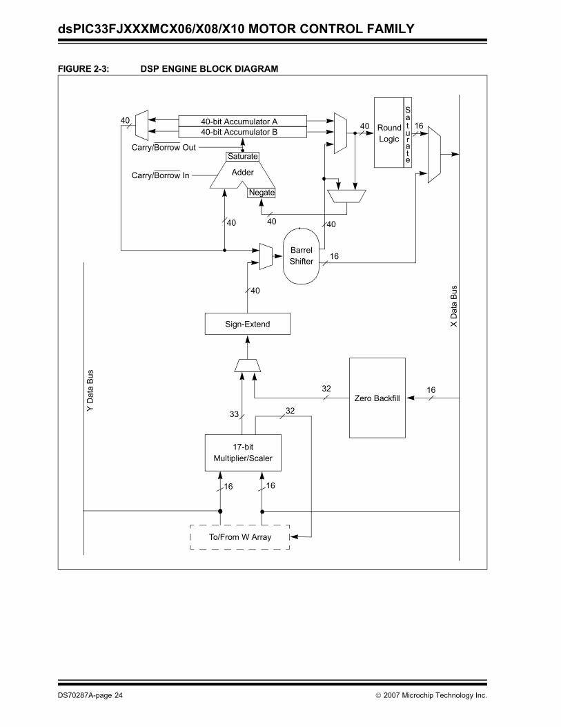
FIGURE 2-3: DSP ENGINE BLOCK DIAGRAM
Zero Backfill
Sign-Extend
BarrelShifter
40-bit Accumulator A40-bit Accumulator B Round
Logic
X D
ata
Bus
To/From W Array
Adder
Saturate
Negate
32
3233
16
16 16
16
40 40
4040
Saturate
Y D
ata
Bus
40
Carry/Borrow Out
Carry/Borrow In
16
40
Multiplier/Scaler17-bit
DS70287A-page 24 © 2007 Microchip Technology Inc.
dsPIC33FJXXXMCX06/X08/X10 MOTOR CONTROL FAMILY
2.6.1 MULTIPLIERThe 17-bit x 17-bit multiplier is capable of signed orunsigned operation and can multiplex its output using ascaler to support either 1.31 fractional (Q31) or 32-bitinteger results. Unsigned operands are zero-extendedinto the 17th bit of the multiplier input value. Signedoperands are sign-extended into the 17th bit of themultiplier input value. The output of the 17-bit x 17-bitmultiplier/scaler is a 33-bit value which issign-extended to 40 bits. Integer data is inherently rep-resented as a signed two’s complement value, wherethe MSb is defined as a sign bit. Generally speaking,the range of an N-bit two’s complement integer is -2N-1
to 2N-1 – 1. For a 16-bit integer, the data range is-32768 (0x8000) to 32767 (0x7FFF) including 0. For a32-bit integer, the data range is -2,147,483,648(0x8000 0000) to 2,147,483,647 (0x7FFF FFFF).
When the multiplier is configured for fractional multipli-cation, the data is represented as a two’s complementfraction, where the MSb is defined as a sign bit and theradix point is implied to lie just after the sign bit (QXformat). The range of an N-bit two’s complementfraction with this implied radix point is -1.0 to (1 – 21-N).For a 16-bit fraction, the Q15 data range is -1.0(0x8000) to 0.999969482 (0x7FFF) including 0 and hasa precision of 3.01518x10⁻⁵. In Fractional mode, the 16x 16 multiply operation generates a 1.31 product whichhas a precision of 4.65661 x 10⁻¹⁰.
The same multiplier is used to support the MCU multi-ply instructions which include integer 16-bit signed,unsigned and mixed sign multiplies.
The MUL instruction may be directed to use byte orword sized operands. Byte operands will direct a 16-bitresult, and word operands will direct a 32-bit result tothe specified register(s) in the W array.
2.6.2 DATA ACCUMULATORS AND ADDER/SUBTRACTER
The data accumulator consists of a 40-bitadder/subtracter with automatic sign extension logic. Itcan select one of two accumulators (A or B) as itspre-accumulation source and post-accumulation desti-nation. For the ADD and LAC instructions, the data to beaccumulated or loaded can be optionally scaled via thebarrel shifter prior to accumulation.
2.6.2.1 Adder/Subtracter, Overflow and Saturation
The adder/subtracter is a 40-bit adder with an optionalzero input into one side, and either true, or complementdata into the other input. In the case of addition, theCarry/Borrow input is active-high and the other input istrue data (not complemented), whereas in the case ofsubtraction, the Carry/Borrow input is active-low andthe other input is complemented. The adder/subtractergenerates Overflow Status bits, SA/SB and OA/OB,which are latched and reflected in the STATUS register:
• Overflow from bit 39: this is a catastrophic overflow in which the sign of the accumulator is destroyed.
• Overflow into guard bits 32 through 39: this is a recoverable overflow. This bit is set whenever all the guard bits are not identical to each other.
The adder has an additional saturation block whichcontrols accumulator data saturation, if selected. Ituses the result of the adder, the Overflow Status bitsdescribed above and the SAT<A:B> (CORCON<7:6>)and ACCSAT (CORCON<4>) mode control bits todetermine when and to what value to saturate.
Six STATUS register bits have been provided tosupport saturation and overflow; they are:
1. OA:AccA overflowed into guard bits
2. OB: AccB overflowed into guard bits
3. SA:AccA saturated (bit 31 overflow and saturation)orAccA overflowed into guard bits and saturated(bit 39 overflow and saturation)
4. SB:AccB saturated (bit 31 overflow and saturation)orAccB overflowed into guard bits and saturated(bit 39 overflow and saturation)
5. OAB:Logical OR of OA and OB
6. SAB:Logical OR of SA and SB
The OA and OB bits are modified each time datapasses through the adder/subtracter. When set, theyindicate that the most recent operation has overflowedinto the accumulator guard bits (bits 32 through 39).The OA and OB bits can also optionally generate anarithmetic warning trap when they and the correspond-ing Overflow Trap Flag Enable bits (OVATE, OVBTE) inthe INTCON1 register (refer to Section 6.0 “InterruptController”) are set. This allows the user to takeimmediate action, for example, to correct system gain.
© 2007 Microchip Technology Inc. DS70287A-page 25
dsPIC33FJXXXMCX06/X08/X10 MOTOR CONTROL FAMILY
The SA and SB bits are modified each time datapasses through the adder/subtracter, but can only becleared by the user. When set, they indicate that theaccumulator has overflowed its maximum range (bit 31for 32-bit saturation or bit 39 for 40-bit saturation) andwill be saturated (if saturation is enabled). Whensaturation is not enabled, SA and SB default to bit 39overflow and, thus, indicate that a catastrophic over-flow has occurred. If the COVTE bit in the INTCON1register is set, SA and SB bits will generate an arithmetic warning trap when saturation is disabled.
The Overflow and Saturation Status bits can optionallybe viewed in the STATUS Register (SR) as the logicalOR of OA and OB (in bit OAB) and the logical OR of SAand SB (in bit SAB). This allows programmers to checkone bit in the STATUS register to determine if eitheraccumulator has overflowed or one bit to determine ifeither accumulator has saturated. This would be usefulfor complex number arithmetic, which typically usesboth the accumulators.
The device supports three Saturation and Overflowmodes:
1. Bit 39 Overflow and Saturation:When bit 39 overflow and saturation occurs, thesaturation logic loads the maximally positive 9.31(0x7FFFFFFFFF) or maximally negative 9.31value (0x8000000000) into the target accumula-tor. The SA or SB bit is set and remains set untilcleared by the user. This is referred to as ‘supersaturation’ and provides protection against erro-neous data or unexpected algorithm problems(e.g., gain calculations).
2. Bit 31 Overflow and Saturation:When bit 31 overflow and saturation occurs, thesaturation logic then loads the maximally posi-tive 1.31 value (0x007FFFFFFF) or maximallynegative 1.31 value (0x0080000000) into thetarget accumulator. The SA or SB bit is set andremains set until cleared by the user. When thisSaturation mode is in effect, the guard bits arenot used (so the OA, OB or OAB bits are neverset).
3. Bit 39 Catastrophic Overflow:The bit 39 Overflow Status bit from the adder isused to set the SA or SB bit, which remains setuntil cleared by the user. No saturation operationis performed and the accumulator is allowed tooverflow (destroying its sign). If the COVTE bit inthe INTCON1 register is set, a catastrophicoverflow can initiate a trap exception.
2.6.2.2 Accumulator ‘Write Back’The MAC class of instructions (with the exception ofMPY, MPY.N, ED and EDAC) can optionally write arounded version of the high word (bits 31 through 16)of the accumulator that is not targeted by the instructioninto data space memory. The write is performed acrossthe X bus into combined X and Y address space. Thefollowing addressing modes are supported:
1. W13, Register Direct:The rounded contents of the non-targetaccumulator are written into W13 as a1.15 fraction.
2. [W13]+ = 2, Register Indirect with Post-Increment:The rounded contents of the non-target accumu-lator are written into the address pointed to byW13 as a 1.15 fraction. W13 is thenincremented by 2 (for a word write).
2.6.2.3 Round LogicThe round logic is a combinational block whichperforms a conventional (biased) or convergent(unbiased) round function during an accumulator write(store). The Round mode is determined by the state ofthe RND bit in the CORCON register. It generates a16-bit, 1.15 data value which is passed to the dataspace write saturation logic. If rounding is not indicatedby the instruction, a truncated 1.15 data value is storedand the least significant word is simply discarded.
Conventional rounding zero-extends bit 15 of the accu-mulator and adds it to the ACCxH word (bits 16 through31 of the accumulator). If the ACCxL word (bits 0through 15 of the accumulator) is between 0x8000 and0xFFFF (0x8000 included), ACCxH is incremented. IfACCxL is between 0x0000 and 0x7FFF, ACCxH is leftunchanged. A consequence of this algorithm is thatover a succession of random rounding operations, thevalue tends to be biased slightly positive.
Convergent (or unbiased) rounding operates in thesame manner as conventional rounding, except whenACCxL equals 0x8000. In this case, the Least Signifi-cant bit (bit 16 of the accumulator) of ACCxH isexamined. If it is ‘1’, ACCxH is incremented. If it is ‘0’,ACCxH is not modified. Assuming that bit 16 iseffectively random in nature, this scheme removes anyrounding bias that may accumulate.
The SAC and SAC.R instructions store either atruncated (SAC), or rounded (SAC.R) version of thecontents of the target accumulator to data memory viathe X bus, subject to data saturation (seeSection 2.6.2.4 “Data Space Write Saturation”). Forthe MAC class of instructions, the accumulatorwrite-back operation will function in the same manner,addressing combined MCU (X and Y) data spacethough the X bus. For this class of instructions, the datais always subject to rounding.
DS70287A-page 26 © 2007 Microchip Technology Inc.
dsPIC33FJXXXMCX06/X08/X10 MOTOR CONTROL FAMILY
2.6.2.4 Data Space Write SaturationIn addition to adder/subtracter saturation, writes to dataspace can also be saturated – but without affecting thecontents of the source accumulator. The data spacewrite saturation logic block accepts a 16-bit, 1.15 frac-tional value from the round logic block as its input,together with overflow status from the original source(accumulator) and the 16-bit round adder. These inputsare combined and used to select the appropriate 1.15fractional value as output to write to data spacememory.
If the SATDW bit in the CORCON register is set, data(after rounding or truncation) is tested for overflow andadjusted accordingly. For input data greater than0x007FFF, data written to memory is forced to the max-imum positive 1.15 value, 0x7FFF. For input data lessthan 0xFF8000, data written to memory is forced to themaximum negative 1.15 value, 0x8000. The MostSignificant bit of the source (bit 39) is used to determinethe sign of the operand being tested.
If the SATDW bit in the CORCON register is not set, theinput data is always passed through unmodified underall conditions.
2.6.3 BARREL SHIFTERThe barrel shifter is capable of performing up to 16-bitarithmetic or logic right shifts, or up to 16-bit left shiftsin a single cycle. The source can be either of the twoDSP accumulators or the X bus (to support multi-bitshifts of register or memory data).
The shifter requires a signed binary value to determineboth the magnitude (number of bits) and direction of theshift operation. A positive value shifts the operand right.A negative value shifts the operand left. A value of ‘0’does not modify the operand.
The barrel shifter is 40 bits wide, thereby obtaining a40-bit result for DSP shift operations and a 16-bit resultfor MCU shift operations. Data from the X bus is pre-sented to the barrel shifter between bit positions 16 to31 for right shifts and between bit positions 0 to 16 forleft shifts.
© 2007 Microchip Technology Inc. DS70287A-page 27

dsPIC33FJXXXMCX06/X08/X10 MOTOR CONTROL FAMILY
NOTES:
DS70287A-page 28 © 2007 Microchip Technology Inc.
dsPIC33FJXXXMCX06/X08/X10 MOTOR CONTROL FAMILY
3.0 MEMORY ORGANIZATION
The dsPIC33FJXXXMCX06/X08/X10 Motor ControlFamily architecture features separate program anddata memory spaces and buses. This architecture alsoallows the direct access of program memory from thedata space during code execution.
3.1 Program Address SpaceThe program address memory space of thedsPIC33FJXXXMCX06/X08/X10 Motor Control Familydevices is 4M instructions. The space is addressableby a 24-bit value derived from either the 23-bit ProgramCounter (PC) during program execution, or from tableoperation or data space remapping as described inSection 3.6 “Interfacing Program and Data MemorySpaces”.
User access to the program memory space is restrictedto the lower half of the address range (0x000000 to0x7FFFFF). The exception is the use of TBLRD/TBLWToperations, which use TBLPAG<7> to permit access tothe Configuration bits and Device ID sections of theconfiguration memory space. Memory usage for thedsPIC33FJXXXMCX06/X08/X10 Motor Control Familyfamily of devices is shown in Figure 3-1.
Note: This data sheet summarizes the featuresof this groupof dsPIC33FJXXXMCX06/X08/X10 MotorControl Family devices. It is not intendedto be a comprehensive reference source.To complement the information in this datasheet, refer to the “dsPIC33F FamilyReference Manual”. Refer to theMicrochip web site (www.microchip.com)for the latest dsPIC33F family referencemanual chapters.
© 2007 Microchip Technology Inc. DS70287A-page 29
dsPIC33FJXXXMCX06/X08/X10 MOTOR CONTROL FAMILY
FIGURE 3-1: PROGRAM MEMORY MAP FOR dsPIC33FJXXXMCX06/X08/X10 MOTOR CONTROL FAMILY DEVICES
Reset Address0x000000
0x0000FE
0x000002
0x000100
Device Configuration
User ProgramFlash Memory
0x00AC000x00ABFE
(22K instructions)
0x800000
0xF80000Registers 0xF80017
0xF80010
DEVID (2)0xFEFFFE0xFF00000xFFFFFE
0xF7FFFE
Unimplemented(Read ‘0’s)
GOTO Instruction0x000004
Reserved
0x7FFFFE
Reserved
0x0002000x0001FE0x000104Alternate Vector Table
ReservedInterrupt Vector Table
Reset Address
Device ConfigurationRegisters
DEVID (2)
Unimplemented(Read ‘0’s)
GOTO Instruction
Reserved
Reserved
Alternate Vector TableReserved
Interrupt Vector TableReset Address
Device Configuration
User ProgramFlash Memory
(88K instructions)
Registers
DEVID (2)
GOTO Instruction
Reserved
Reserved
Alternate Vector TableReserved
Interrupt Vector Table
dsPIC33FJ64MCXXX dsPIC33FJ128MCXXX dsPIC33FJ256MCXXXC
onfig
urat
ion
Mem
ory
Spac
eU
ser M
emor
y Sp
ace
0x0158000x0157FE
User Program
(44K instructions)Flash Memory
(Read ‘0’s)Unimplemented
0x02AC000x02ABFE
DS70287A-page 30 © 2007 Microchip Technology Inc.
dsPIC33FJXXXMCX06/X08/X10 MOTOR CONTROL FAMILY
3.1.1 PROGRAM MEMORY ORGANIZATION
The program memory space is organized inword-addressable blocks. Although it is treated as24 bits wide, it is more appropriate to think of eachaddress of the program memory as a lower and upperword, with the upper byte of the upper word beingunimplemented. The lower word always has an evenaddress, while the upper word has an odd address(Figure 3-2).
Program memory addresses are always word-alignedon the lower word, and addresses are incremented ordecremented by two during code execution. Thisarrangement also provides compatibility with datamemory space addressing and makes it possible toaccess data in the program memory space.
3.1.2 INTERRUPT AND TRAP VECTORSAll dsPIC33FJXXXMCX06/X08/X10 Motor ControlFamily devices reserve the addresses between0x00000 and 0x000200 for hard-coded program exe-cution vectors. A hardware Reset vector is provided toredirect code execution from the default value of thePC on device Reset to the actual start of code. A GOTOinstruction is programmed by the user at 0x000000,with the actual address for the start of code at0x000002.
dsPIC33FJXXXMCX06/X08/X10 Motor Control Familydevices also have two interrupt vector tables locatedfrom 0x000004 to 0x0000FF and 0x000100 to0x0001FF. These vector tables allow each of the manydevice interrupt sources to be handled by separateInterrupt Service Routines (ISRs). A more detailed dis-cussion of the interrupt vector tables is provided inSection 6.1 “Interrupt Vector Table”.
FIGURE 3-2: PROGRAM MEMORY ORGANIZATION
0816
PC Address
0x0000000x0000020x0000040x000006
230000000000000000
0000000000000000
Program Memory‘Phantom’ Byte
(read as ‘0’)
least significant wordmost significant word
Instruction Width
0x0000010x0000030x0000050x000007
mswAddress (lsw Address)
© 2007 Microchip Technology Inc. DS70287A-page 31
dsPIC33FJXXXMCX06/X08/X10 MOTOR CONTROL FAMILY
3.2 Data Address SpaceThe dsPIC33FJXXXMCX06/X08/X10 Motor ControlFamily CPU has a separate 16-bit wide data memoryspace. The data space is accessed using separateAddress Generation Units (AGUs) for read and writeoperations. Data memory maps of devices with differ-ent RAM sizes are shown in Figure 3-3 throughFigure 3-5.
All Effective Addresses (EAs) in the data memory spaceare 16 bits wide and point to bytes within the data space.This arrangement gives a data space address range of64 Kbytes or 32K words. The lower half of the datamemory space (that is, when EA<15> = 0) is used forimplemented memory addresses, while the upper half(EA<15> = 1) is reserved for the Program SpaceVisibility area (see Section 3.6.3 “Reading Data FromProgram Memory Using Program Space Visibility”).
dsPIC33FJXXXMCX06/X08/X10 Motor Control Familydevices implement a total of up to 30 Kbytes of datamemory. Should an EA point to a location outside ofthis area, an all-zero word or byte will be returned.
3.2.1 DATA SPACE WIDTHThe data memory space is organized in byteaddressable, 16-bit wide blocks. Data is aligned in datamemory and registers as 16-bit words, but all dataspace EAs resolve to bytes. The Least SignificantBytes of each word have even addresses, while theMost Significant Bytes have odd addresses.
3.2.2 DATA MEMORY ORGANIZATION AND ALIGNMENT
To maintain backward compatibility with PIC® micro-controllers and improve data space memory usageefficiency, the dsPIC33FJXXXMCX06/X08/X10 MotorControl Family instruction set supports both word andbyte operations. As a consequence of byte accessibil-ity, all effective address calculations are internallyscaled to step through word-aligned memory. Forexample, the core recognizes that Post-ModifiedRegister Indirect Addressing mode [Ws++] will result ina value of Ws + 1 for byte operations and Ws + 2 forword operations.
Data byte reads will read the complete word thatcontains the byte, using the LSb of any EA to determinewhich byte to select. The selected byte is placed ontothe LSb of the data path. That is, data memory and reg-isters are organized as two parallel byte-wide entitieswith shared (word) address decode but separate writelines. Data byte writes only write to the correspondingside of the array or register which matches the byteaddress.
All word accesses must be aligned to an even address.Misaligned word data fetches are not supported, socare must be taken when mixing byte and wordoperations or translating from 8-bit MCU code. If amisaligned read or write is attempted, an address errortrap is generated. If the error occurred on a read, theinstruction underway is completed; if it occurred on awrite, the instruction will be executed but the write doesnot occur. In either case, a trap is then executed,allowing the system and/or user to examine themachine state prior to execution of the address Fault.
All byte loads into any W register are loaded into theLeast Significant Byte. The Most Significant Byte is notmodified.
A sign-extend instruction (SE) is provided to allowusers to translate 8-bit signed data to 16-bit signedvalues. Alternatively, for 16-bit unsigned data, userscan clear the MSb of any W register by executing azero-extend (ZE) instruction on the appropriateaddress.
3.2.3 SFR SPACEThe first 2 Kbytes of the Near Data Space, from 0x0000to 0x07FF, is primarily occupied by Special FunctionRegisters (SFRs). These are used by thedsPIC33FJXXXMCX06/X08/X10 Motor Control Familycore and peripheral modules for controlling theoperation of the device.
SFRs are distributed among the modules that theycontrol and are generally grouped together by module.Much of the SFR space contains unused addresses;these are read as ‘0’.
3.2.4 NEAR DATA SPACE The 8-Kbyte area between 0x0000 and 0x1FFF isreferred to as the Near Data Space. Locations in thisspace are directly addressable via a 13-bit absoluteaddress field within all memory direct instructions.Additionally, the whole data space is addressable usingMOV instructions, which support Memory DirectAddressing mode with a 16-bit address field, or byusing Indirect Addressing mode using a workingregister as an Address Pointer.
Note: The actual set of peripheral features andinterrupts varies by the device. Pleaserefer to the corresponding device tablesand pinout diagrams for device-specificinformation.
DS70287A-page 32 © 2007 Microchip Technology Inc.
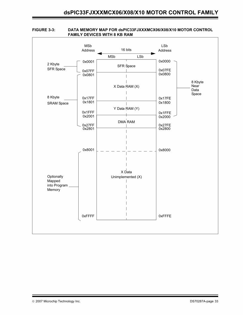
dsPIC33FJXXXMCX06/X08/X10 MOTOR CONTROL FAMILY
FIGURE 3-3: DATA MEMORY MAP FOR dsPIC33FJXXXMCX06/X08/X10 MOTOR CONTROL FAMILY DEVICES WITH 8 KB RAM
0x0000
0x07FE
0x17FE
0xFFFE
LSbAddress16 bits
LSbMSb
MSbAddress
0x0001
0x07FF
0x17FF
0xFFFF
OptionallyMappedinto ProgramMemory
0x27FF 0x27FE
0x0801 0x0800
0x1801 0x1800
2 KbyteSFR Space
8 Kbyte
SRAM Space
0x8001 0x8000
0x28000x2801
0x1FFE0x2000
0x1FFF0x2001
SpaceDataNear8 Kbyte
SFR Space
X Data RAM (X)
X DataUnimplemented (X)
DMA RAM
Y Data RAM (Y)
© 2007 Microchip Technology Inc. DS70287A-page 33
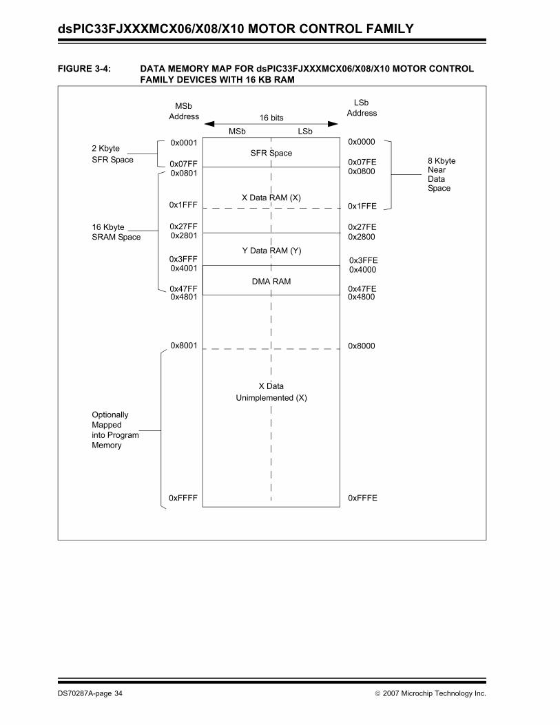
dsPIC33FJXXXMCX06/X08/X10 MOTOR CONTROL FAMILY
FIGURE 3-4: DATA MEMORY MAP FOR dsPIC33FJXXXMCX06/X08/X10 MOTOR CONTROL FAMILY DEVICES WITH 16 KB RAM
0x0000
0x07FE
0x27FE
0xFFFE
LSbAddress16 bits
LSbMSb
MSbAddress
0x0001
0x07FF
0x27FF
0xFFFF
OptionallyMappedinto ProgramMemory
0x47FF 0x47FE
0x0801 0x0800
0x2801 0x2800
NearData
2 KbyteSFR Space
16 KbyteSRAM Space
8 Kbyte
Space
0x8001 0x8000
0x48000x4801
0x3FFE0x4000
0x3FFF0x4001
0x1FFE0x1FFF
SFR Space
X Data RAM (X)
X DataUnimplemented (X)
DMA RAM
Y Data RAM (Y)
DS70287A-page 34 © 2007 Microchip Technology Inc.
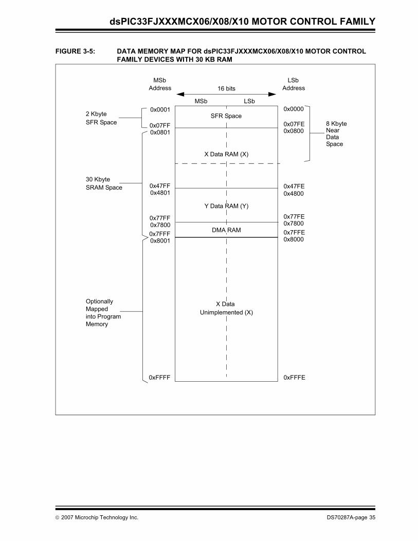
dsPIC33FJXXXMCX06/X08/X10 MOTOR CONTROL FAMILY
FIGURE 3-5: DATA MEMORY MAP FOR dsPIC33FJXXXMCX06/X08/X10 MOTOR CONTROL FAMILY DEVICES WITH 30 KB RAM
0x0000
0x07FESFR Space
0xFFFE
X Data RAM (X)
16 bits
LSbMSb0x0001
0x07FF
0xFFFF
X Data OptionallyMappedinto ProgramMemory
Unimplemented (X)
0x0801 0x0800
2 KbyteSFR Space
0x48000x47FE
0x48010x47FF
0x7FFE0x8000
30 KbyteSRAM Space
0x7FFF0x8001
Y Data RAM (Y)
NearData
8 Kbyte
Space
0x77FE0x7800
0x77FF0x7800
LSbAddress
MSbAddress
DMA RAM
© 2007 Microchip Technology Inc. DS70287A-page 35
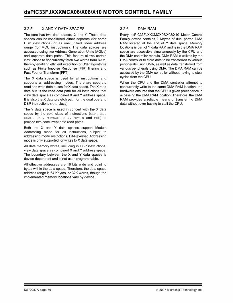
dsPIC33FJXXXMCX06/X08/X10 MOTOR CONTROL FAMILY
3.2.5 X AND Y DATA SPACESThe core has two data spaces, X and Y. These dataspaces can be considered either separate (for someDSP instructions) or as one unified linear addressrange (for MCU instructions). The data spaces areaccessed using two Address Generation Units (AGUs)and separate data paths. This feature allows certaininstructions to concurrently fetch two words from RAM,thereby enabling efficient execution of DSP algorithmssuch as Finite Impulse Response (FIR) filtering andFast Fourier Transform (FFT).
The X data space is used by all instructions andsupports all addressing modes. There are separateread and write data buses for X data space. The X readdata bus is the read data path for all instructions thatview data space as combined X and Y address space.It is also the X data prefetch path for the dual operandDSP instructions (MAC class).
The Y data space is used in concert with the X dataspace by the MAC class of instructions (CLR, ED,EDAC, MAC, MOVSAC, MPY, MPY.N and MSC) toprovide two concurrent data read paths.
Both the X and Y data spaces support ModuloAddressing mode for all instructions, subject toaddressing mode restrictions. Bit-Reversed Addressingmode is only supported for writes to X data space.
All data memory writes, including in DSP instructions,view data space as combined X and Y address space.The boundary between the X and Y data spaces isdevice-dependent and is not user-programmable.
All effective addresses are 16 bits wide and point tobytes within the data space. Therefore, the data spaceaddress range is 64 Kbytes, or 32K words, though theimplemented memory locations vary by device.
3.2.6 DMA RAMEvery dsPIC33FJXXXMCX06/X08/X10 Motor ControlFamily device contains 2 Kbytes of dual ported DMARAM located at the end of Y data space. Memorylocations is part of Y data RAM and is in the DMA RAMspace are accessible simultaneously by the CPU andthe DMA controller module. DMA RAM is utilized by theDMA controller to store data to be transferred to variousperipherals using DMA, as well as data transferred fromvarious peripherals using DMA. The DMA RAM can beaccessed by the DMA controller without having to stealcycles from the CPU.
When the CPU and the DMA controller attempt toconcurrently write to the same DMA RAM location, thehardware ensures that the CPU is given precedence inaccessing the DMA RAM location. Therefore, the DMARAM provides a reliable means of transferring DMAdata without ever having to stall the CPU.
DS70287A-page 36 © 2007 Microchip Technology Inc.
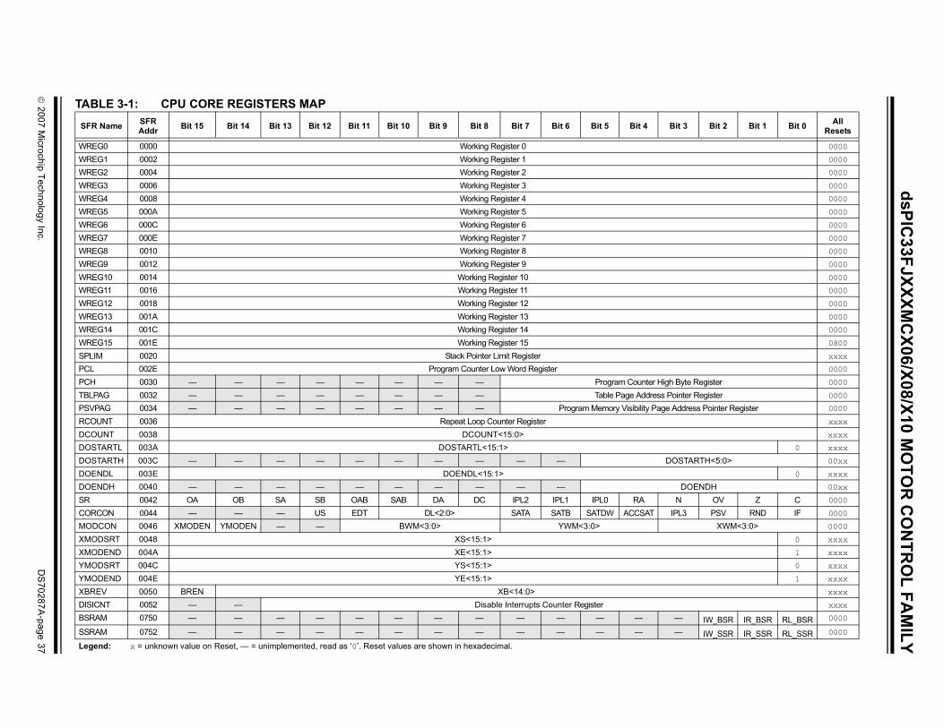
© 2007 M
icrochip Technology Inc.D
S70287A
-page 37
dsPIC33FJXXXM
CX06/X08/X10 M
OTO
R C
ON
TRO
L FAM
ILY
TA
S Bit 3 Bit 2 Bit 1 Bit 0 All Resets
W 0000
W 0000
W 0000
W 0000
W 0000
W 0000
W 0000
W 0000
W 0000
W 0000
W 0000
W 0000
W 0000
W 0000
W 0000
W 0800
SP xxxx
PC 0000
PC h Byte Register 0000
TB Pointer Register 0000
PS Address Pointer Register 0000
RC xxxx
DC xxxx
DO 0 xxxx
DO DOSTARTH<5:0> 00xx
DO 0 xxxx
DO DOENDH 00xx
SR N OV Z C 0000
CO IPL3 PSV RND IF 0000
MO XWM<3:0> 0000
XM 0 xxxx
XM 1 xxxx
YM 0 xxxx
YM 1 xxxx
XB xxxx
DI xxxx
BS — IW_BSR IR_BSR RL_BSR 0000
SS — IW_SSR IR_SSR RL_SSR 0000
Le
BLE 3-1: CPU CORE REGISTERS MAP
FR Name SFR Addr Bit 15 Bit 14 Bit 13 Bit 12 Bit 11 Bit 10 Bit 9 Bit 8 Bit 7 Bit 6 Bit 5 Bit 4
REG0 0000 Working Register 0REG1 0002 Working Register 1REG2 0004 Working Register 2REG3 0006 Working Register 3REG4 0008 Working Register 4REG5 000A Working Register 5REG6 000C Working Register 6REG7 000E Working Register 7REG8 0010 Working Register 8REG9 0012 Working Register 9REG10 0014 Working Register 10REG11 0016 Working Register 11REG12 0018 Working Register 12REG13 001A Working Register 13REG14 001C Working Register 14REG15 001E Working Register 15LIM 0020 Stack Pointer Limit RegisterL 002E Program Counter Low Word RegisterH 0030 — — — — — — — — Program Counter HigLPAG 0032 — — — — — — — — Table Page Address VPAG 0034 — — — — — — — — Program Memory Visibility PageOUNT 0036 Repeat Loop Counter RegisterOUNT 0038 DCOUNT<15:0>STARTL 003A DOSTARTL<15:1>STARTH 003C — — — — — — — — — —ENDL 003E DOENDL<15:1>ENDH 0040 — — — — — — — — — —
0042 OA OB SA SB OAB SAB DA DC IPL2 IPL1 IPL0 RARCON 0044 — — — US EDT DL<2:0> SATA SATB SATDW ACCSATDCON 0046 XMODEN YMODEN — — BWM<3:0> YWM<3:0>ODSRT 0048 XS<15:1>ODEND 004A XE<15:1>ODSRT 004C YS<15:1>ODEND 004E YE<15:1>REV 0050 BREN XB<14:0>
SICNT 0052 — — Disable Interrupts Counter RegisterRAM 0750 — — — — — — — — — — — —
RAM 0752 — — — — — — — — — — — —
gend: x = unknown value on Reset, — = unimplemented, read as ‘0’. Reset values are shown in hexadecimal.
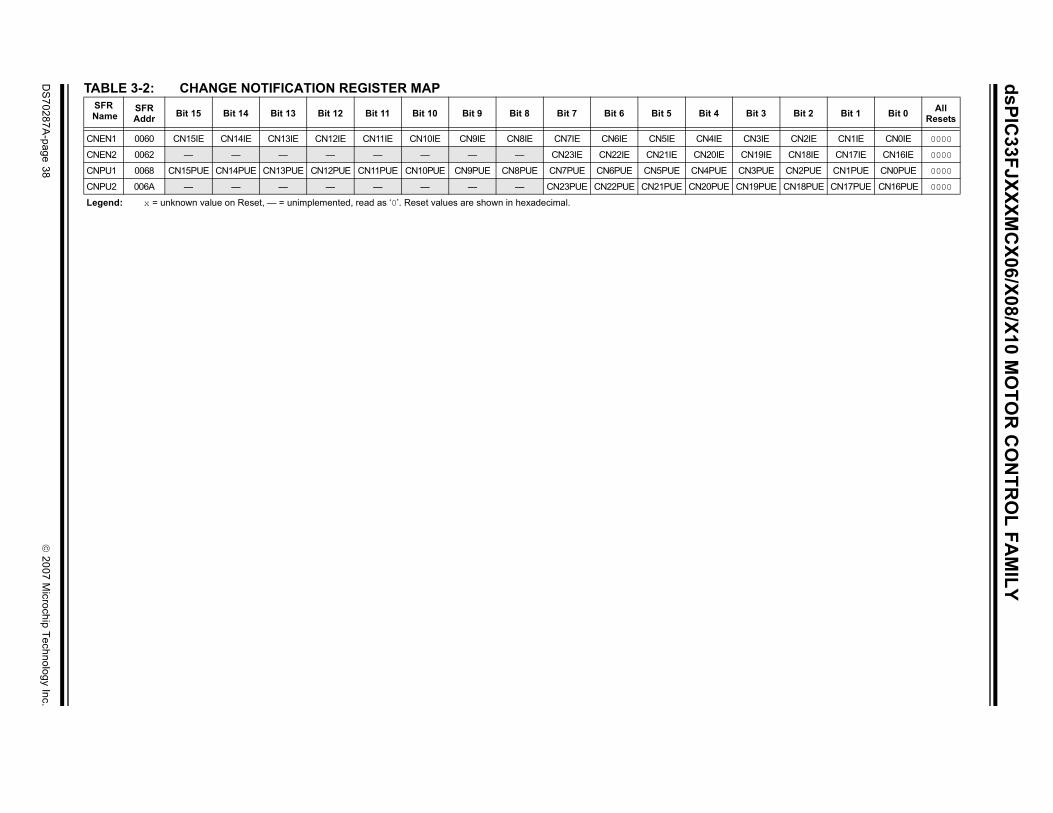
dsPIC33FJXXXM
CX06/X08/X10 M
OTO
R C
ON
TRO
L FAM
ILY
DS
70287A-page 38
© 2007 M
icrochip Technology Inc.
Bit 3 Bit 2 Bit 1 Bit 0 All Resets
CN3IE CN2IE CN1IE CN0IE 0000
E CN19IE CN18IE CN17IE CN16IE 0000
E CN3PUE CN2PUE CN1PUE CN0PUE 0000
E CN19PUE CN18PUE CN17PUE CN16PUE 0000
TABLE 3-2: CHANGE NOTIFICATION REGISTER MAPSFR
NameSFR Addr Bit 15 Bit 14 Bit 13 Bit 12 Bit 11 Bit 10 Bit 9 Bit 8 Bit 7 Bit 6 Bit 5 Bit 4
CNEN1 0060 CN15IE CN14IE CN13IE CN12IE CN11IE CN10IE CN9IE CN8IE CN7IE CN6IE CN5IE CN4IE
CNEN2 0062 — — — — — — — — CN23IE CN22IE CN21IE CN20I
CNPU1 0068 CN15PUE CN14PUE CN13PUE CN12PUE CN11PUE CN10PUE CN9PUE CN8PUE CN7PUE CN6PUE CN5PUE CN4PU
CNPU2 006A — — — — — — — — CN23PUE CN22PUE CN21PUE CN20PU
Legend: x = unknown value on Reset, — = unimplemented, read as ‘0’. Reset values are shown in hexadecimal.
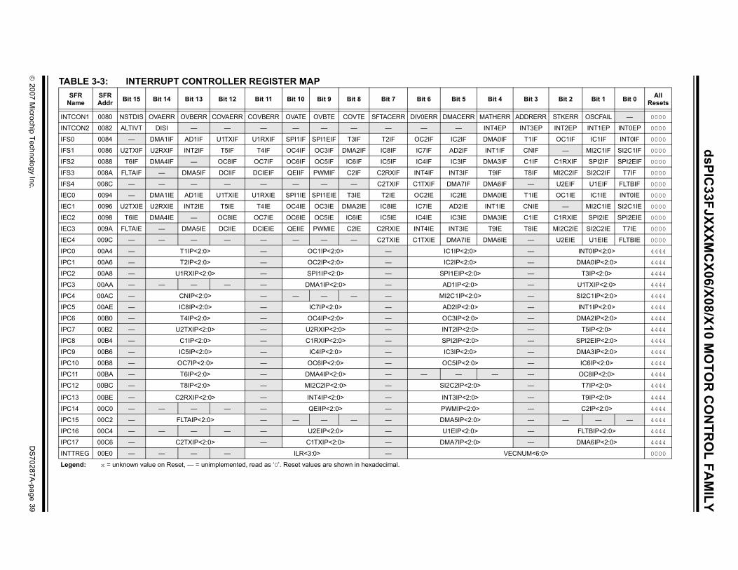
© 2007 M
icrochip Technology Inc.D
S70287A
-page 39
dsPIC33FJXXXM
CX06/X08/X10 M
OTO
R C
ON
TRO
L FAM
ILY
TA
N Bit 3 Bit 2 Bit 1 Bit 0 AllResets
IN DRERR STKERR OSCFAIL — 0000
IN NT3EP INT2EP INT1EP INT0EP 0000
IFS T1IF OC1IF IC1IF INT0IF 0000
IFS CNIF — MI2C1IF SI2C1IF 0000
IFS C1IF C1RXIF SPI2IF SPI2EIF 0000
IFS T8IF MI2C2IF SI2C2IF T7IF 0000
IFS — U2EIF U1EIF FLTBIF 0000
IEC T1IE OC1IE IC1IE INT0IE 0000
IEC CNIE — MI2C1IE SI2C1IE 0000
IEC C1IE C1RXIE SPI2IE SPI2EIE 0000
IEC T8IE MI2C2IE SI2C2IE T7IE 0000
IEC — U2EIE U1EIE FLTBIE 0000
IPC — INT0IP<2:0> 4444
IPC — DMA0IP<2:0> 4444
IPC — T3IP<2:0> 4444
IPC — U1TXIP<2:0> 4444
IPC — SI2C1IP<2:0> 4444
IPC — INT1IP<2:0> 4444
IPC — DMA2IP<2:0> 4444
IPC — T5IP<2:0> 4444
IPC — SPI2EIP<2:0> 4444
IPC — DMA3IP<2:0> 4444
IPC — IC6IP<2:0> 4444
IPC — OC8IP<2:0> 4444
IPC — T7IP<2:0> 4444
IPC — T9IP<2:0> 4444
IPC — C2IP<2:0> 4444
IPC — — — — 4444
IPC — FLTBIP<2:0> 4444
IPC — DMA6IP<2:0> 4444
IN UM<6:0> 0000
Le
BLE 3-3: INTERRUPT CONTROLLER REGISTER MAPSFR ame
SFR Addr Bit 15 Bit 14 Bit 13 Bit 12 Bit 11 Bit 10 Bit 9 Bit 8 Bit 7 Bit 6 Bit 5 Bit 4
TCON1 0080 NSTDIS OVAERR OVBERR COVAERR COVBERR OVATE OVBTE COVTE SFTACERR DIV0ERR DMACERR MATHERR AD
TCON2 0082 ALTIVT DISI — — — — — — — — — INT4EP I
0 0084 — DMA1IF AD1IF U1TXIF U1RXIF SPI1IF SPI1EIF T3IF T2IF OC2IF IC2IF DMA0IF
1 0086 U2TXIF U2RXIF INT2IF T5IF T4IF OC4IF OC3IF DMA2IF IC8IF IC7IF AD2IF INT1IF
2 0088 T6IF DMA4IF — OC8IF OC7IF OC6IF OC5IF IC6IF IC5IF IC4IF IC3IF DMA3IF
3 008A FLTAIF — DMA5IF DCIIF DCIEIF QEIIF PWMIF C2IF C2RXIF INT4IF INT3IF T9IF
4 008C — — — — — — — — C2TXIF C1TXIF DMA7IF DMA6IF
0 0094 — DMA1IE AD1IE U1TXIE U1RXIE SPI1IE SPI1EIE T3IE T2IE OC2IE IC2IE DMA0IE
1 0096 U2TXIE U2RXIE INT2IE T5IE T4IE OC4IE OC3IE DMA2IE IC8IE IC7IE AD2IE INT1IE
2 0098 T6IE DMA4IE — OC8IE OC7IE OC6IE OC5IE IC6IE IC5IE IC4IE IC3IE DMA3IE
3 009A FLTAIE — DMA5IE DCIIE DCIEIE QEIIE PWMIE C2IE C2RXIE INT4IE INT3IE T9IE
4 009C — — — — — — — — C2TXIE C1TXIE DMA7IE DMA6IE
0 00A4 — T1IP<2:0> — OC1IP<2:0> — IC1IP<2:0>
1 00A6 — T2IP<2:0> — OC2IP<2:0> — IC2IP<2:0>
2 00A8 — U1RXIP<2:0> — SPI1IP<2:0> — SPI1EIP<2:0>
3 00AA — — — — — DMA1IP<2:0> — AD1IP<2:0>
4 00AC — CNIP<2:0> — — — — — MI2C1IP<2:0>
5 00AE — IC8IP<2:0> — IC7IP<2:0> — AD2IP<2:0>
6 00B0 — T4IP<2:0> — OC4IP<2:0> — OC3IP<2:0>
7 00B2 — U2TXIP<2:0> — U2RXIP<2:0> — INT2IP<2:0>
8 00B4 — C1IP<2:0> — C1RXIP<2:0> — SPI2IP<2:0>
9 00B6 — IC5IP<2:0> — IC4IP<2:0> — IC3IP<2:0>
10 00B8 — OC7IP<2:0> — OC6IP<2:0> — OC5IP<2:0>
11 00BA — T6IP<2:0> — DMA4IP<2:0> — — — —
12 00BC — T8IP<2:0> — MI2C2IP<2:0> — SI2C2IP<2:0>
13 00BE — C2RXIP<2:0> — INT4IP<2:0> — INT3IP<2:0>
14 00C0 — — — — — QEIIP<2:0> — PWMIP<2:0>
15 00C2 — FLTAIP<2:0> — — — — — DMA5IP<2:0>
16 00C4 — — — — — U2EIP<2:0> — U1EIP<2:0>
17 00C6 — C2TXIP<2:0> — C1TXIP<2:0> — DMA7IP<2:0>
TTREG 00E0 — — — — ILR<3:0> — VECN
gend: x = unknown value on Reset, — = unimplemented, read as ‘0’. Reset values are shown in hexadecimal.
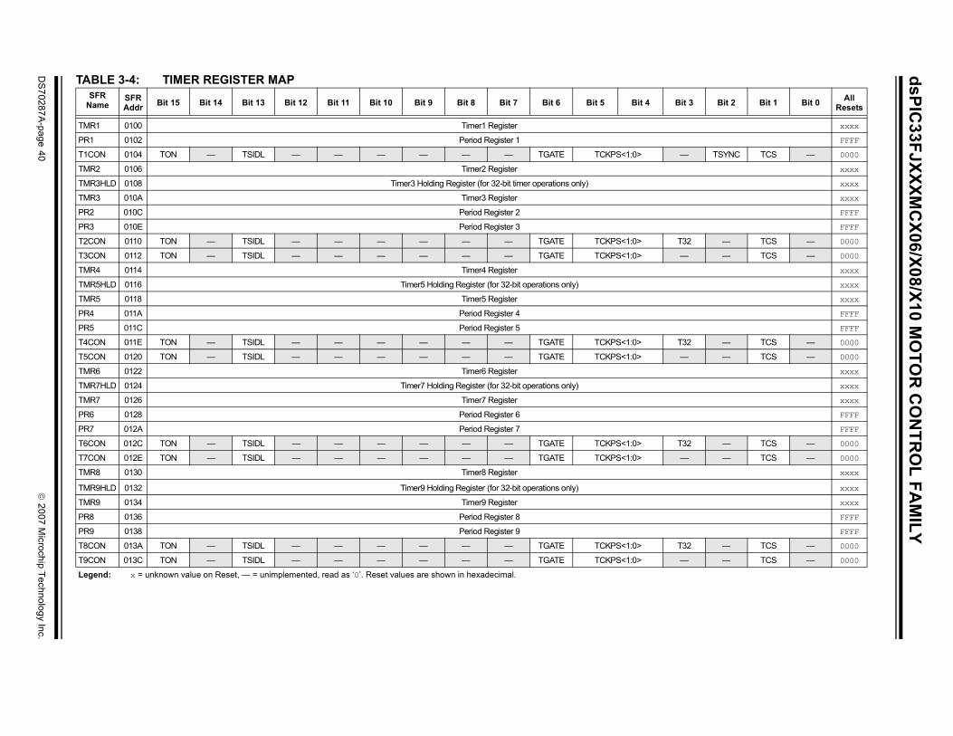
dsPIC33FJXXXM
CX06/X08/X10 M
OTO
R C
ON
TRO
L FAM
ILY
DS
70287A-page 40
© 2007 M
icrochip Technology Inc.
Bit 3 Bit 2 Bit 1 Bit 0 All Resets
xxxx
FFFF
— TSYNC TCS — 0000
xxxx
xxxx
xxxx
FFFF
FFFF
T32 — TCS — 0000
— — TCS — 0000
xxxx
xxxx
xxxx
FFFF
FFFF
T32 — TCS — 0000
— — TCS — 0000
xxxx
xxxx
xxxx
FFFF
FFFF
T32 — TCS — 0000
— — TCS — 0000
xxxx
xxxx
xxxx
FFFF
FFFF
T32 — TCS — 0000
— — TCS — 0000
TABLE 3-4: TIMER REGISTER MAPSFR
NameSFR Addr Bit 15 Bit 14 Bit 13 Bit 12 Bit 11 Bit 10 Bit 9 Bit 8 Bit 7 Bit 6 Bit 5 Bit 4
TMR1 0100 Timer1 Register
PR1 0102 Period Register 1
T1CON 0104 TON — TSIDL — — — — — — TGATE TCKPS<1:0>
TMR2 0106 Timer2 Register
TMR3HLD 0108 Timer3 Holding Register (for 32-bit timer operations only)
TMR3 010A Timer3 Register
PR2 010C Period Register 2
PR3 010E Period Register 3
T2CON 0110 TON — TSIDL — — — — — — TGATE TCKPS<1:0>
T3CON 0112 TON — TSIDL — — — — — — TGATE TCKPS<1:0>
TMR4 0114 Timer4 Register
TMR5HLD 0116 Timer5 Holding Register (for 32-bit operations only)
TMR5 0118 Timer5 Register
PR4 011A Period Register 4
PR5 011C Period Register 5
T4CON 011E TON — TSIDL — — — — — — TGATE TCKPS<1:0>
T5CON 0120 TON — TSIDL — — — — — — TGATE TCKPS<1:0>
TMR6 0122 Timer6 Register
TMR7HLD 0124 Timer7 Holding Register (for 32-bit operations only)
TMR7 0126 Timer7 Register
PR6 0128 Period Register 6
PR7 012A Period Register 7
T6CON 012C TON — TSIDL — — — — — — TGATE TCKPS<1:0>
T7CON 012E TON — TSIDL — — — — — — TGATE TCKPS<1:0>
TMR8 0130 Timer8 Register
TMR9HLD 0132 Timer9 Holding Register (for 32-bit operations only)
TMR9 0134 Timer9 Register
PR8 0136 Period Register 8
PR9 0138 Period Register 9
T8CON 013A TON — TSIDL — — — — — — TGATE TCKPS<1:0>
T9CON 013C TON — TSIDL — — — — — — TGATE TCKPS<1:0>
Legend: x = unknown value on Reset, — = unimplemented, read as ‘0’. Reset values are shown in hexadecimal.
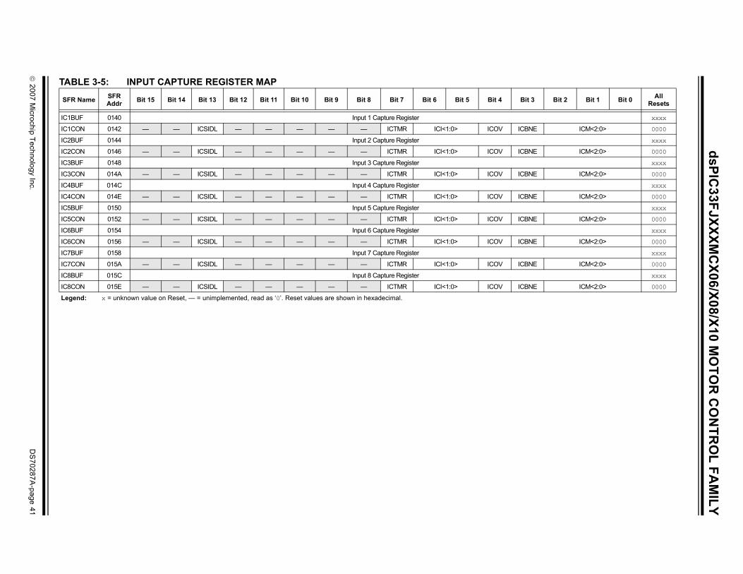
© 2007 M
icrochip Technology Inc.D
S70287A
-page 41
dsPIC33FJXXXM
CX06/X08/X10 M
OTO
R C
ON
TRO
L FAM
ILY
TA
SF it 3 Bit 2 Bit 1 Bit 0 All Resets
IC1 xxxx
IC1 BNE ICM<2:0> 0000
IC2 xxxx
IC2 BNE ICM<2:0> 0000
IC3 xxxx
IC3 BNE ICM<2:0> 0000
IC4 xxxx
IC4 BNE ICM<2:0> 0000
IC5 xxxx
IC5 BNE ICM<2:0> 0000
IC6 xxxx
IC6 BNE ICM<2:0> 0000
IC7 xxxx
IC7 BNE ICM<2:0> 0000
IC8 xxxx
IC8 BNE ICM<2:0> 0000
Le
BLE 3-5: INPUT CAPTURE REGISTER MAP
R Name SFR Addr Bit 15 Bit 14 Bit 13 Bit 12 Bit 11 Bit 10 Bit 9 Bit 8 Bit 7 Bit 6 Bit 5 Bit 4 B
BUF 0140 Input 1 Capture Register
CON 0142 — — ICSIDL — — — — — ICTMR ICI<1:0> ICOV IC
BUF 0144 Input 2 Capture Register
CON 0146 — — ICSIDL — — — — — ICTMR ICI<1:0> ICOV IC
BUF 0148 Input 3 Capture Register
CON 014A — — ICSIDL — — — — — ICTMR ICI<1:0> ICOV IC
BUF 014C Input 4 Capture Register
CON 014E — — ICSIDL — — — — — ICTMR ICI<1:0> ICOV IC
BUF 0150 Input 5 Capture Register
CON 0152 — — ICSIDL — — — — — ICTMR ICI<1:0> ICOV IC
BUF 0154 Input 6 Capture Register
CON 0156 — — ICSIDL — — — — — ICTMR ICI<1:0> ICOV IC
BUF 0158 Input 7 Capture Register
CON 015A — — ICSIDL — — — — — ICTMR ICI<1:0> ICOV IC
BUF 015C Input 8 Capture Register
CON 015E — — ICSIDL — — — — — ICTMR ICI<1:0> ICOV IC
gend: x = unknown value on Reset, — = unimplemented, read as ‘0’. Reset values are shown in hexadecimal.
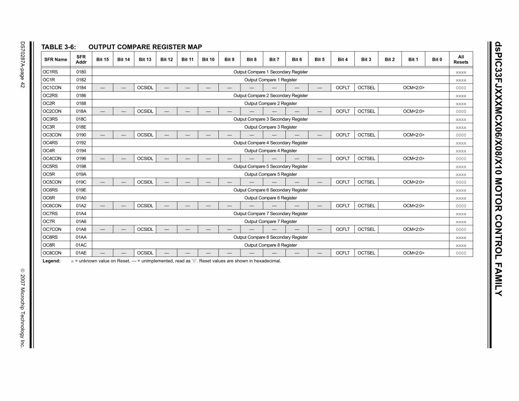
dsPIC33FJXXXM
CX06/X08/X10 M
OTO
R C
ON
TRO
L FAM
ILY
DS
70287A-page 42
© 2007 M
icrochip Technology Inc.
Bit 3 Bit 2 Bit 1 Bit 0 All Resets
xxxx
xxxx
OCTSEL OCM<2:0> 0000
xxxx
xxxx
OCTSEL OCM<2:0> 0000
xxxx
xxxx
OCTSEL OCM<2:0> 0000
xxxx
xxxx
OCTSEL OCM<2:0> 0000
xxxx
xxxx
OCTSEL OCM<2:0> 0000
xxxx
xxxx
OCTSEL OCM<2:0> 0000
xxxx
xxxx
OCTSEL OCM<2:0> 0000
xxxx
xxxx
OCTSEL OCM<2:0> 0000
TABLE 3-6: OUTPUT COMPARE REGISTER MAP
SFR Name SFR Addr Bit 15 Bit 14 Bit 13 Bit 12 Bit 11 Bit 10 Bit 9 Bit 8 Bit 7 Bit 6 Bit 5 Bit 4
OC1RS 0180 Output Compare 1 Secondary Register
OC1R 0182 Output Compare 1 Register
OC1CON 0184 — — OCSIDL — — — — — — — — OCFLT
OC2RS 0186 Output Compare 2 Secondary Register
OC2R 0188 Output Compare 2 Register
OC2CON 018A — — OCSIDL — — — — — — — — OCFLT
OC3RS 018C Output Compare 3 Secondary Register
OC3R 018E Output Compare 3 Register
OC3CON 0190 — — OCSIDL — — — — — — — — OCFLT
OC4RS 0192 Output Compare 4 Secondary Register
OC4R 0194 Output Compare 4 Register
OC4CON 0196 — — OCSIDL — — — — — — — — OCFLT
OC5RS 0198 Output Compare 5 Secondary Register
OC5R 019A Output Compare 5 Register
OC5CON 019C — — OCSIDL — — — — — — — — OCFLT
OC6RS 019E Output Compare 6 Secondary Register
OC6R 01A0 Output Compare 6 Register
OC6CON 01A2 — — OCSIDL — — — — — — — — OCFLT
OC7RS 01A4 Output Compare 7 Secondary Register
OC7R 01A6 Output Compare 7 Register
OC7CON 01A8 — — OCSIDL — — — — — — — — OCFLT
OC8RS 01AA Output Compare 8 Secondary Register
OC8R 01AC Output Compare 8 Register
OC8CON 01AE — — OCSIDL — — — — — — — — OCFLT
Legend: x = unknown value on Reset, — = unimplemented, read as ‘0’. Reset values are shown in hexadecimal.
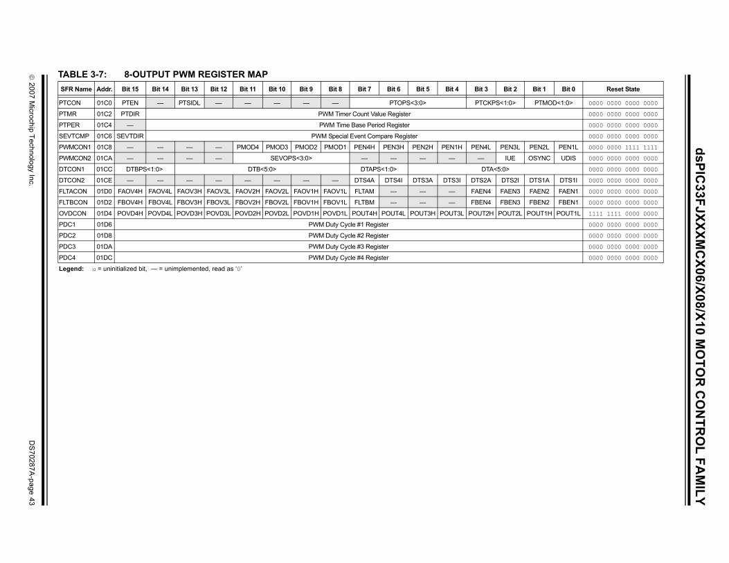
© 2007 M
icrochip Technology Inc.D
S70287A
-page 43
dsPIC33FJXXXM
CX06/X08/X10 M
OTO
R C
ON
TRO
L FAM
ILY
TBit 1 Bit 0 Reset State
P PTMOD<1:0> 0000 0000 0000 0000
P 0000 0000 0000 0000
P 0000 0000 0000 0000
S 0000 0000 0000 0000
P L PEN2L PEN1L 0000 0000 1111 1111
P OSYNC UDIS 0000 0000 0000 0000
D 0000 0000 0000 0000
D 2I DTS1A DTS1I 0000 0000 0000 0000
F 3 FAEN2 FAEN1 0000 0000 0000 0000
F 3 FBEN2 FBEN1 0000 0000 0000 0000
O 2L POUT1H POUT1L 1111 1111 0000 0000
P 0000 0000 0000 0000
P 0000 0000 0000 0000
P 0000 0000 0000 0000
P 0000 0000 0000 0000
L
ABLE 3-7: 8-OUTPUT PWM REGISTER MAPSFR Name Addr. Bit 15 Bit 14 Bit 13 Bit 12 Bit 11 Bit 10 Bit 9 Bit 8 Bit 7 Bit 6 Bit 5 Bit 4 Bit 3 Bit 2
TCON 01C0 PTEN — PTSIDL — — — — — PTOPS<3:0> PTCKPS<1:0>
TMR 01C2 PTDIR PWM Timer Count Value Register
TPER 01C4 — PWM Time Base Period Register
EVTCMP 01C6 SEVTDIR PWM Special Event Compare Register
WMCON1 01C8 — — — — PMOD4 PMOD3 PMOD2 PMOD1 PEN4H PEN3H PEN2H PEN1H PEN4L PEN3
WMCON2 01CA — — — — SEVOPS<3:0> — — — — — IUE
TCON1 01CC DTBPS<1:0> DTB<5:0> DTAPS<1:0> DTA<5:0>
TCON2 01CE — — — — — — — — DTS4A DTS4I DTS3A DTS3I DTS2A DTS
LTACON 01D0 FAOV4H FAOV4L FAOV3H FAOV3L FAOV2H FAOV2L FAOV1H FAOV1L FLTAM — — — FAEN4 FAEN
LTBCON 01D2 FBOV4H FBOV4L FBOV3H FBOV3L FBOV2H FBOV2L FBOV1H FBOV1L FLTBM — — — FBEN4 FBEN
VDCON 01D4 POVD4H POVD4L POVD3H POVD3L POVD2H POVD2L POVD1H POVD1L POUT4H POUT4L POUT3H POUT3L POUT2H POUT
DC1 01D6 PWM Duty Cycle #1 Register
DC2 01D8 PWM Duty Cycle #2 Register
DC3 01DA PWM Duty Cycle #3 Register
DC4 01DC PWM Duty Cycle #4 Register
egend: u = uninitialized bit, — = unimplemented, read as ‘0’
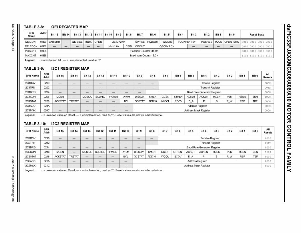
dsPIC33FJXXXM
CX06/X08/X10 M
OTO
R C
ON
TRO
L FAM
ILY
DS
70287A-page 44
© 2007 M
icrochip Technology Inc.
it 2 Bit 1 Bit 0 Reset State
RES TQCS UPDN_SRC 0000 0000 0000 0000
— — — 0000 0000 0000 0000
0000 0000 0000 0000
1111 1111 1111 1111
Bit 3 Bit 2 Bit 1 Bit 0 All Resets
ive Register 0000
smit Register 00FF
rator Register 0000
N RCEN PEN RSEN SEN 1000
S R_W RBF TBF 0000
r 0000
ister 0000
Bit 3 Bit 2 Bit 1 Bit 0 All Resets
ive Register 0000
mit Register 00FF
rator Register 0000
N RCEN PEN RSEN SEN 1000
S R_W RBF TBF 0000
r 0000
ster 0000
TABLE 3-8: QEI REGISTER MAPSFR
NameAddr
. Bit 15 Bit 14 Bit 13 Bit 12 Bit 11 Bit 10 Bit 9 Bit 8 Bit 7 Bit 6 Bit 5 Bit 4 Bit 3 B
QEICON 01E0 CNTERR — QEISIDL INDX UPDN QEIM<2:0> SWPAB PCDOUT TQGATE TQCKPS<1:0> POS
DFLTCON 01E2 — — — — — IMV<1:0> CEID QEOUT QECK<2:0> —
POSCNT 01E4 Position Counter<15:0>
MAXCNT 01E6 Maximum Count<15:0>
Legend: u = uninitialized bit, — = unimplemented, read as ‘0’
TABLE 3-9: I2C1 REGISTER MAP
SFR Name SFR Addr Bit 15 Bit 14 Bit 13 Bit 12 Bit 11 Bit 10 Bit 9 Bit 8 Bit 7 Bit 6 Bit 5 Bit 4
I2C1RCV 0200 — — — — — — — — Rece
I2C1TRN 0202 — — — — — — — — Tran
I2C1BRG 0204 — — — — — — — Baud Rate Gene
I2C1CON 0206 I2CEN — I2CSIDL SCLREL IPMIEN A10M DISSLW SMEN GCEN STREN ACKDT ACKE
I2C1STAT 0208 ACKSTAT TRSTAT — — — BCL GCSTAT ADD10 IWCOL I2COV D_A P
I2C1ADD 020A — — — — — — Address Registe
I2C1MSK 020C — — — — — — Address Mask Reg
Legend: x = unknown value on Reset, — = unimplemented, read as ‘0’. Reset values are shown in hexadecimal.
TABLE 3-10: I2C2 REGISTER MAP
SFR Name SFR Addr Bit 15 Bit 14 Bit 13 Bit 12 Bit 11 Bit 10 Bit 9 Bit 8 Bit 7 Bit 6 Bit 5 Bit 4
I2C2RCV 0210 — — — — — — — — Rece
I2C2TRN 0212 — — — — — — — — Trans
I2C2BRG 0214 — — — — — — — Baud Rate Gene
I2C2CON 0216 I2CEN — I2CSIDL SCLREL IPMIEN A10M DISSLW SMEN GCEN STREN ACKDT ACKE
I2C2STAT 0218 ACKSTAT TRSTAT — — — BCL GCSTAT ADD10 IWCOL I2COV D_A P
I2C2ADD 021A — — — — — — Address Registe
I2C2MSK 021C — — — — — — Address Mask Regi
Legend: x = unknown value on Reset, — = unimplemented, read as ‘0’. Reset values are shown in hexadecimal.
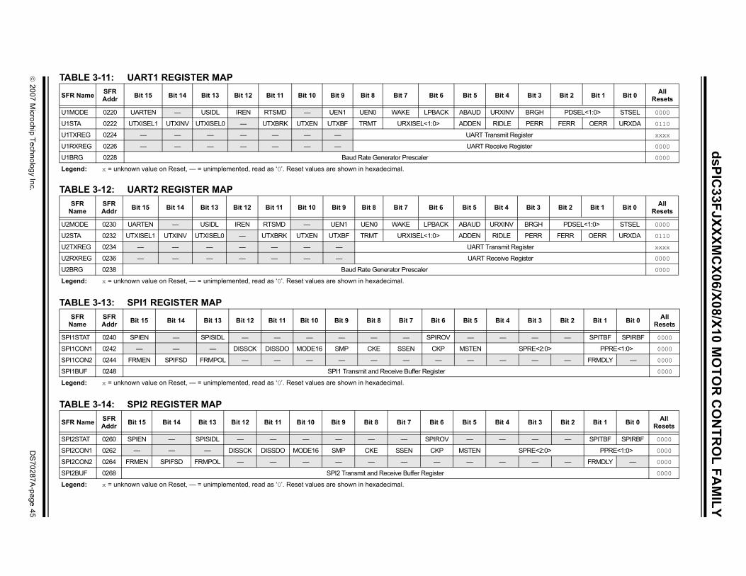
© 2007 M
icrochip Technology Inc.D
S70287A
-page 45
dsPIC33FJXXXM
CX06/X08/X10 M
OTO
R C
ON
TRO
L FAM
ILY
T
S Bit 3 Bit 2 Bit 1 Bit 0 All Resets
U RGH PDSEL<1:0> STSEL 0000
U PERR FERR OERR URXDA 0110
U er xxxx
U er 0000
U 0000
L
T
Bit 3 Bit 2 Bit 1 Bit 0 All Resets
U RGH PDSEL<1:0> STSEL 0000
U ERR FERR OERR URXDA 0110
U ter xxxx
U ter 0000
U 0000
L
T
Bit 3 Bit 2 Bit 1 Bit 0 All Resets
S — — SPITBF SPIRBF 0000
S RE<2:0> PPRE<1:0> 0000
S — — FRMDLY — 0000
S 0000
L
T
S Bit 3 Bit 2 Bit 1 Bit 0 All Resets
S — — SPITBF SPIRBF 0000
S RE<2:0> PPRE<1:0> 0000
S — — FRMDLY — 0000
S 0000
L
ABLE 3-11: UART1 REGISTER MAP
FR Name SFR Addr Bit 15 Bit 14 Bit 13 Bit 12 Bit 11 Bit 10 Bit 9 Bit 8 Bit 7 Bit 6 Bit 5 Bit 4
1MODE 0220 UARTEN — USIDL IREN RTSMD — UEN1 UEN0 WAKE LPBACK ABAUD URXINV B
1STA 0222 UTXISEL1 UTXINV UTXISEL0 — UTXBRK UTXEN UTXBF TRMT URXISEL<1:0> ADDEN RIDLE
1TXREG 0224 — — — — — — — UART Transmit Regist
1RXREG 0226 — — — — — — — UART Receive Regist
1BRG 0228 Baud Rate Generator Prescaler
egend: x = unknown value on Reset, — = unimplemented, read as ‘0’. Reset values are shown in hexadecimal.
ABLE 3-12: UART2 REGISTER MAPSFR
NameSFR Addr Bit 15 Bit 14 Bit 13 Bit 12 Bit 11 Bit 10 Bit 9 Bit 8 Bit 7 Bit 6 Bit 5 Bit 4
2MODE 0230 UARTEN — USIDL IREN RTSMD — UEN1 UEN0 WAKE LPBACK ABAUD URXINV B
2STA 0232 UTXISEL1 UTXINV UTXISEL0 — UTXBRK UTXEN UTXBF TRMT URXISEL<1:0> ADDEN RIDLE P
2TXREG 0234 — — — — — — — UART Transmit Regis
2RXREG 0236 — — — — — — — UART Receive Regis
2BRG 0238 Baud Rate Generator Prescaler
egend: x = unknown value on Reset, — = unimplemented, read as ‘0’. Reset values are shown in hexadecimal.
ABLE 3-13: SPI1 REGISTER MAPSFR
NameSFR Addr Bit 15 Bit 14 Bit 13 Bit 12 Bit 11 Bit 10 Bit 9 Bit 8 Bit 7 Bit 6 Bit 5 Bit 4
PI1STAT 0240 SPIEN — SPISIDL — — — — — — SPIROV — —
PI1CON1 0242 — — — DISSCK DISSDO MODE16 SMP CKE SSEN CKP MSTEN SP
PI1CON2 0244 FRMEN SPIFSD FRMPOL — — — — — — — — —
PI1BUF 0248 SPI1 Transmit and Receive Buffer Register
egend: x = unknown value on Reset, — = unimplemented, read as ‘0’. Reset values are shown in hexadecimal.
ABLE 3-14: SPI2 REGISTER MAP
FR Name SFR Addr Bit 15 Bit 14 Bit 13 Bit 12 Bit 11 Bit 10 Bit 9 Bit 8 Bit 7 Bit 6 Bit 5 Bit 4
PI2STAT 0260 SPIEN — SPISIDL — — — — — — SPIROV — —
PI2CON1 0262 — — — DISSCK DISSDO MODE16 SMP CKE SSEN CKP MSTEN SP
PI2CON2 0264 FRMEN SPIFSD FRMPOL — — — — — — — — —
PI2BUF 0268 SPI2 Transmit and Receive Buffer Register
egend: x = unknown value on Reset, — = unimplemented, read as ‘0’. Reset values are shown in hexadecimal.
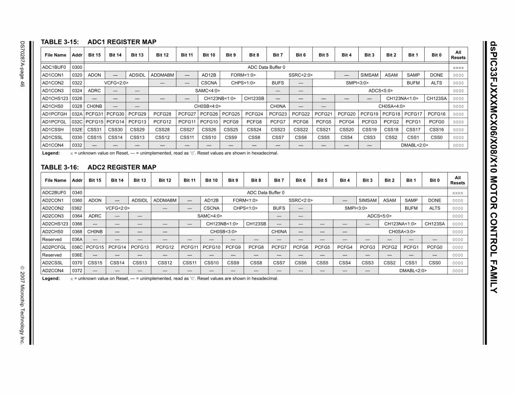
dsPIC33FJXXXM
CX06/X08/X10 M
OTO
R C
ON
TRO
L FAM
ILY
DS
70287A-page 46
© 2007 M
icrochip Technology Inc.
Bit 3 Bit 2 Bit 1 Bit 0 All Resets
xxxx
SIMSAM ASAM SAMP DONE 0000
PI<3:0> BUFM ALTS 0000
ADCS<5:0> 0000
— CH123NA<1:0> CH123SA 0000
CH0SA<4:0> 0000
0 PCFG19 PCFG18 PCFG17 PCFG16 0000
4 PCFG3 PCFG2 PCFG1 PCFG0 0000
0 CSS19 CSS18 CSS17 CSS16 0000
CSS3 CSS2 CSS1 CSS0 0000
— DMABL<2:0> 0000
Bit 3 Bit 2 Bit 1 Bit 0 All Resets
xxxx
SIMSAM ASAM SAMP DONE 0000
PI<3:0> BUFM ALTS 0000
ADCS<5:0> 0000
— CH123NA<1:0> CH123SA 0000
CH0SA<3:0> 0000
— — — — 0000
PCFG3 PCFG2 PCFG1 PCFG0 0000
— — — — 0000
CSS3 CSS2 CSS1 CSS0 0000
— DMABL<2:0> 0000
TABLE 3-15: ADC1 REGISTER MAP
File Name Addr Bit 15 Bit 14 Bit 13 Bit 12 Bit 11 Bit 10 Bit 9 Bit 8 Bit 7 Bit 6 Bit 5 Bit 4
ADC1BUF0 0300 ADC Data Buffer 0
AD1CON1 0320 ADON — ADSIDL ADDMABM — AD12B FORM<1:0> SSRC<2:0> —
AD1CON2 0322 VCFG<2:0> — — CSCNA CHPS<1:0> BUFS — SM
AD1CON3 0324 ADRC — — SAMC<4:0> — —
AD1CHS123 0326 — — — — — CH123NB<1:0> CH123SB — — — —
AD1CHS0 0328 CH0NB — — CH0SB<4:0> CH0NA — —
AD1PCFGH 032A PCFG31 PCFG30 PCFG29 PCFG28 PCFG27 PCFG26 PCFG25 PCFG24 PCFG23 PCFG22 PCFG21 PCFG2
AD1PCFGL 032C PCFG15 PCFG14 PCFG13 PCFG12 PCFG11 PCFG10 PCFG9 PCFG8 PCFG7 PCFG6 PCFG5 PCFG
AD1CSSH 032E CSS31 CSS30 CSS29 CSS28 CSS27 CSS26 CSS25 CSS24 CSS23 CSS22 CSS21 CSS2
AD1CSSL 0330 CSS15 CSS14 CSS13 CSS12 CSS11 CSS10 CSS9 CSS8 CSS7 CSS6 CSS5 CSS4
AD1CON4 0332 — — — — — — — — — — — —
Legend: x = unknown value on Reset, — = unimplemented, read as ‘0’. Reset values are shown in hexadecimal.
TABLE 3-16: ADC2 REGISTER MAP
File Name Addr Bit 15 Bit 14 Bit 13 Bit 12 Bit 11 Bit 10 Bit 9 Bit 8 Bit 7 Bit 6 Bit 5 Bit 4
ADC2BUF0 0340 ADC Data Buffer 0
AD2CON1 0360 ADON — ADSIDL ADDMABM — AD12B FORM<1:0> SSRC<2:0> —
AD2CON2 0362 VCFG<2:0> — — CSCNA CHPS<1:0> BUFS — SM
AD2CON3 0364 ADRC — — SAMC<4:0> — —
AD2CHS123 0366 — — — — — CH123NB<1:0> CH123SB — — — —
AD2CHS0 0368 CH0NB — — — CH0SB<3:0> CH0NA — — —
Reserved 036A — — — — — — — — — — — —
AD2PCFGL 036C PCFG15 PCFG14 PCFG13 PCFG12 PCFG11 PCFG10 PCFG9 PCFG8 PCFG7 PCFG6 PCFG5 PCFG4
Reserved 036E — — — — — — — — — — — —
AD2CSSL 0370 CSS15 CSS14 CSS13 CSS12 CSS11 CSS10 CSS9 CSS8 CSS7 CSS6 CSS5 CSS4
AD2CON4 0372 — — — — — — — — — — — —
Legend: x = unknown value on Reset, — = unimplemented, read as ‘0’. Reset values are shown in hexadecimal.
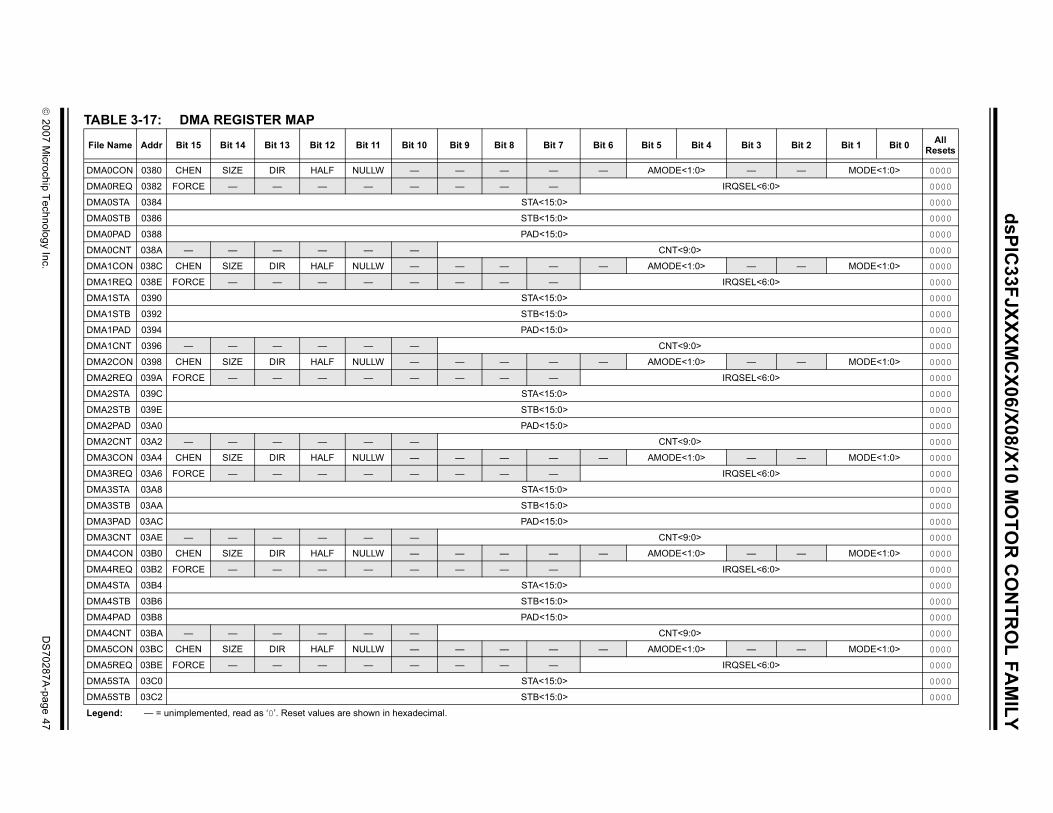
© 2007 M
icrochip Technology Inc.D
S70287A
-page 47
dsPIC33FJXXXM
CX06/X08/X10 M
OTO
R C
ON
TRO
L FAM
ILY
TA
File it 3 Bit 2 Bit 1 Bit 0 All Resets
DM — — MODE<1:0> 0000
DM EL<6:0> 0000
DM 0000
DM 0000
DM 0000
DM 0000
DM — — MODE<1:0> 0000
DM EL<6:0> 0000
DM 0000
DM 0000
DM 0000
DM 0000
DM — — MODE<1:0> 0000
DM EL<6:0> 0000
DM 0000
DM 0000
DM 0000
DM 0000
DM — — MODE<1:0> 0000
DM EL<6:0> 0000
DM 0000
DM 0000
DM 0000
DM 0000
DM — — MODE<1:0> 0000
DM EL<6:0> 0000
DM 0000
DM 0000
DM 0000
DM 0000
DM — — MODE<1:0> 0000
DM EL<6:0> 0000
DM 0000
DM 0000
Leg
BLE 3-17: DMA REGISTER MAP
Name Addr Bit 15 Bit 14 Bit 13 Bit 12 Bit 11 Bit 10 Bit 9 Bit 8 Bit 7 Bit 6 Bit 5 Bit 4 B
A0CON 0380 CHEN SIZE DIR HALF NULLW — — — — — AMODE<1:0>
A0REQ 0382 FORCE — — — — — — — — IRQS
A0STA 0384 STA<15:0>
A0STB 0386 STB<15:0>
A0PAD 0388 PAD<15:0>
A0CNT 038A — — — — — — CNT<9:0>
A1CON 038C CHEN SIZE DIR HALF NULLW — — — — — AMODE<1:0>
A1REQ 038E FORCE — — — — — — — — IRQS
A1STA 0390 STA<15:0>
A1STB 0392 STB<15:0>
A1PAD 0394 PAD<15:0>
A1CNT 0396 — — — — — — CNT<9:0>
A2CON 0398 CHEN SIZE DIR HALF NULLW — — — — — AMODE<1:0>
A2REQ 039A FORCE — — — — — — — — IRQS
A2STA 039C STA<15:0>
A2STB 039E STB<15:0>
A2PAD 03A0 PAD<15:0>
A2CNT 03A2 — — — — — — CNT<9:0>
A3CON 03A4 CHEN SIZE DIR HALF NULLW — — — — — AMODE<1:0>
A3REQ 03A6 FORCE — — — — — — — — IRQS
A3STA 03A8 STA<15:0>
A3STB 03AA STB<15:0>
A3PAD 03AC PAD<15:0>
A3CNT 03AE — — — — — — CNT<9:0>
A4CON 03B0 CHEN SIZE DIR HALF NULLW — — — — — AMODE<1:0>
A4REQ 03B2 FORCE — — — — — — — — IRQS
A4STA 03B4 STA<15:0>
A4STB 03B6 STB<15:0>
A4PAD 03B8 PAD<15:0>
A4CNT 03BA — — — — — — CNT<9:0>
A5CON 03BC CHEN SIZE DIR HALF NULLW — — — — — AMODE<1:0>
A5REQ 03BE FORCE — — — — — — — — IRQS
A5STA 03C0 STA<15:0>
A5STB 03C2 STB<15:0>
end: — = unimplemented, read as ‘0’. Reset values are shown in hexadecimal.
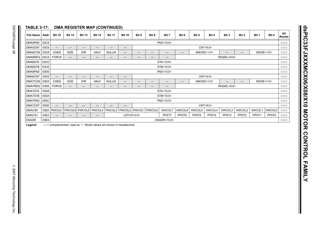
dsPIC33FJXXXM
CX06/X08/X10 M
OTO
R C
ON
TRO
L FAM
ILY
DS
70287A-page 48
© 2007 M
icrochip Technology Inc.
0000
0000
— — MODE<1:0> 0000
IRQSEL<6:0> 0000
0000
0000
0000
0000
— — MODE<1:0> 0000
IRQSEL<6:0> 0000
0000
0000
0000
0000
XWCOL3 XWCOL2 XWCOL1 XWCOL0 0000
PPST3 PPST2 PPST1 PPST0 0000
0000
Bit 3 Bit 2 Bit 1 Bit 0 All Resets
DMA5PAD 03C4 PAD<15:0>
DMA5CNT 03C6 — — — — — — CNT<9:0>
DMA6CON 03C8 CHEN SIZE DIR HALF NULLW — — — — — AMODE<1:0>
DMA6REQ 03CA FORCE — — — — — — — —
DMA6STA 03CC STA<15:0>
DMA6STB 03CE STB<15:0>
DMA6PAD 03D0 PAD<15:0>
DMA6CNT 03D2 — — — — — — CNT<9:0>
DMA7CON 03D4 CHEN SIZE DIR HALF NULLW — — — — — AMODE<1:0>
DMA7REQ 03D6 FORCE — — — — — — — —
DMA7STA 03D8 STA<15:0>
DMA7STB 03DA STB<15:0>
DMA7PAD 03DC PAD<15:0>
DMA7CNT 03DE — — — — — — CNT<9:0>
DMACS0 03E0 PWCOL7 PWCOL6 PWCOL5 PWCOL4 PWCOL3 PWCOL2 PWCOL1 PWCOL0 XWCOL7 XWCOL6 XWCOL5 XWCOL4
DMACS1 03E2 — — — — LSTCH<3:0> PPST7 PPST6 PPST5 PPST4
DSADR 03E4 DSADR<15:0>
TABLE 3-17: DMA REGISTER MAP (CONTINUED)
File Name Addr Bit 15 Bit 14 Bit 13 Bit 12 Bit 11 Bit 10 Bit 9 Bit 8 Bit 7 Bit 6 Bit 5 Bit 4
Legend: — = unimplemented, read as ‘0’. Reset values are shown in hexadecimal.
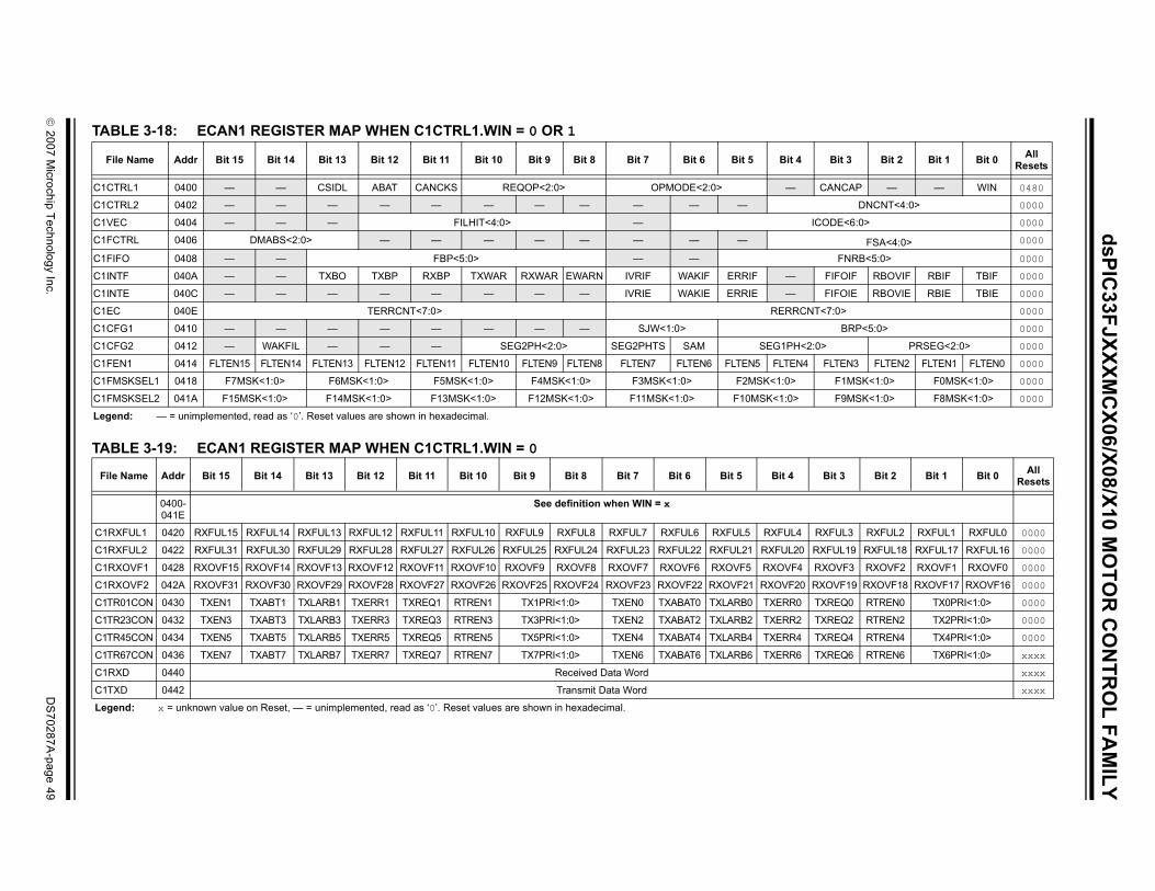
© 2007 M
icrochip Technology Inc.D
S70287A
-page 49
dsPIC33FJXXXM
CX06/X08/X10 M
OTO
R C
ON
TRO
L FAM
ILY
TA
F Bit 3 Bit 2 Bit 1 Bit 0 All Resets
C1C CANCAP — — WIN 0480
C1C DNCNT<4:0> 0000
C1V CODE<6:0> 0000
C1F FSA<4:0> 0000
C1F FNRB<5:0> 0000
C1I FIFOIF RBOVIF RBIF TBIF 0000
C1I FIFOIE RBOVIE RBIE TBIE 0000
C1E T<7:0> 0000
C1C BRP<5:0> 0000
C1C 0> PRSEG<2:0> 0000
C1F FLTEN3 FLTEN2 FLTEN1 FLTEN0 0000
C1F F1MSK<1:0> F0MSK<1:0> 0000
C1F F9MSK<1:0> F8MSK<1:0> 0000
Leg
TA
Fi Bit 3 Bit 2 Bit 1 Bit 0 All Resets
C1 RXFUL3 RXFUL2 RXFUL1 RXFUL0 0000
C1 XFUL19 RXFUL18 RXFUL17 RXFUL16 0000
C1 RXOVF3 RXOVF2 RXOVF1 RXOVF0 0000
C1 XOVF19 RXOVF18 RXOVF17 RXOVF16 0000
C1T TXREQ0 RTREN0 TX0PRI<1:0> 0000
C1T TXREQ2 RTREN2 TX2PRI<1:0> 0000
C1T TXREQ4 RTREN4 TX4PRI<1:0> 0000
C1T TXREQ6 RTREN6 TX6PRI<1:0> xxxx
C1 xxxx
C1T xxxx
Leg
BLE 3-18: ECAN1 REGISTER MAP WHEN C1CTRL1.WIN = 0 OR 1
ile Name Addr Bit 15 Bit 14 Bit 13 Bit 12 Bit 11 Bit 10 Bit 9 Bit 8 Bit 7 Bit 6 Bit 5 Bit 4
TRL1 0400 — — CSIDL ABAT CANCKS REQOP<2:0> OPMODE<2:0> —
TRL2 0402 — — — — — — — — — — —
EC 0404 — — — FILHIT<4:0> — I
CTRL 0406 DMABS<2:0> — — — — — — — —
IFO 0408 — — FBP<5:0> — —
NTF 040A — — TXBO TXBP RXBP TXWAR RXWAR EWARN IVRIF WAKIF ERRIF —
NTE 040C — — — — — — — — IVRIE WAKIE ERRIE —
C 040E TERRCNT<7:0> RERRCN
FG1 0410 — — — — — — — — SJW<1:0>
FG2 0412 — WAKFIL — — — SEG2PH<2:0> SEG2PHTS SAM SEG1PH<2:
EN1 0414 FLTEN15 FLTEN14 FLTEN13 FLTEN12 FLTEN11 FLTEN10 FLTEN9 FLTEN8 FLTEN7 FLTEN6 FLTEN5 FLTEN4
MSKSEL1 0418 F7MSK<1:0> F6MSK<1:0> F5MSK<1:0> F4MSK<1:0> F3MSK<1:0> F2MSK<1:0>
MSKSEL2 041A F15MSK<1:0> F14MSK<1:0> F13MSK<1:0> F12MSK<1:0> F11MSK<1:0> F10MSK<1:0>
end: — = unimplemented, read as ‘0’. Reset values are shown in hexadecimal.
BLE 3-19: ECAN1 REGISTER MAP WHEN C1CTRL1.WIN = 0
le Name Addr Bit 15 Bit 14 Bit 13 Bit 12 Bit 11 Bit 10 Bit 9 Bit 8 Bit 7 Bit 6 Bit 5 Bit 4
0400-041E
See definition when WIN = x
RXFUL1 0420 RXFUL15 RXFUL14 RXFUL13 RXFUL12 RXFUL11 RXFUL10 RXFUL9 RXFUL8 RXFUL7 RXFUL6 RXFUL5 RXFUL4
RXFUL2 0422 RXFUL31 RXFUL30 RXFUL29 RXFUL28 RXFUL27 RXFUL26 RXFUL25 RXFUL24 RXFUL23 RXFUL22 RXFUL21 RXFUL20 R
RXOVF1 0428 RXOVF15 RXOVF14 RXOVF13 RXOVF12 RXOVF11 RXOVF10 RXOVF9 RXOVF8 RXOVF7 RXOVF6 RXOVF5 RXOVF4
RXOVF2 042A RXOVF31 RXOVF30 RXOVF29 RXOVF28 RXOVF27 RXOVF26 RXOVF25 RXOVF24 RXOVF23 RXOVF22 RXOVF21 RXOVF20 R
R01CON 0430 TXEN1 TXABT1 TXLARB1 TXERR1 TXREQ1 RTREN1 TX1PRI<1:0> TXEN0 TXABAT0 TXLARB0 TXERR0
R23CON 0432 TXEN3 TXABT3 TXLARB3 TXERR3 TXREQ3 RTREN3 TX3PRI<1:0> TXEN2 TXABAT2 TXLARB2 TXERR2
R45CON 0434 TXEN5 TXABT5 TXLARB5 TXERR5 TXREQ5 RTREN5 TX5PRI<1:0> TXEN4 TXABAT4 TXLARB4 TXERR4
R67CON 0436 TXEN7 TXABT7 TXLARB7 TXERR7 TXREQ7 RTREN7 TX7PRI<1:0> TXEN6 TXABAT6 TXLARB6 TXERR6
RXD 0440 Received Data Word
XD 0442 Transmit Data Word
end: x = unknown value on Reset, — = unimplemented, read as ‘0’. Reset values are shown in hexadecimal.
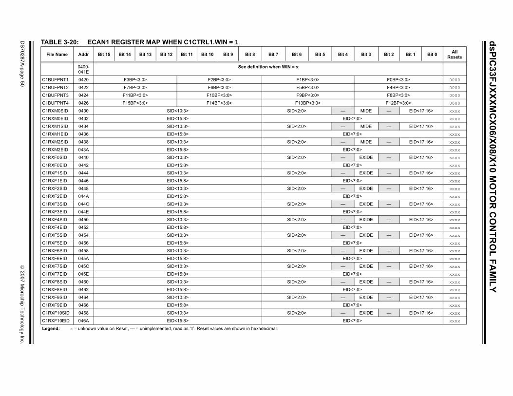
dsPIC33FJXXXM
CX06/X08/X10 M
OTO
R C
ON
TRO
L FAM
ILY
DS
70287A-page 50
© 2007 M
icrochip Technology Inc.
Bit 3 Bit 2 Bit 1 Bit 0 All Resets
F0BP<3:0> 0000
F4BP<3:0> 0000
F8BP<3:0> 0000
F12BP<3:0> 0000
MIDE — EID<17:16> xxxx
<7:0> xxxx
MIDE — EID<17:16> xxxx
<7:0> xxxx
MIDE — EID<17:16> xxxx
<7:0> xxxx
EXIDE — EID<17:16> xxxx
<7:0> xxxx
EXIDE — EID<17:16> xxxx
<7:0> xxxx
EXIDE — EID<17:16> xxxx
<7:0> xxxx
EXIDE — EID<17:16> xxxx
<7:0> xxxx
EXIDE — EID<17:16> xxxx
<7:0> xxxx
EXIDE — EID<17:16> xxxx
<7:0> xxxx
EXIDE — EID<17:16> xxxx
<7:0> xxxx
EXIDE — EID<17:16> xxxx
<7:0> xxxx
EXIDE — EID<17:16> xxxx
<7:0> xxxx
EXIDE — EID<17:16> xxxx
<7:0> xxxx
EXIDE — EID<17:16> xxxx
<7:0> xxxx
TABLE 3-20: ECAN1 REGISTER MAP WHEN C1CTRL1.WIN = 1
File Name Addr Bit 15 Bit 14 Bit 13 Bit 12 Bit 11 Bit 10 Bit 9 Bit 8 Bit 7 Bit 6 Bit 5 Bit 4
0400-041E
See definition when WIN = x
C1BUFPNT1 0420 F3BP<3:0> F2BP<3:0> F1BP<3:0>
C1BUFPNT2 0422 F7BP<3:0> F6BP<3:0> F5BP<3:0>
C1BUFPNT3 0424 F11BP<3:0> F10BP<3:0> F9BP<3:0>
C1BUFPNT4 0426 F15BP<3:0> F14BP<3:0> F13BP<3:0>
C1RXM0SID 0430 SID<10:3> SID<2:0> —
C1RXM0EID 0432 EID<15:8> EID
C1RXM1SID 0434 SID<10:3> SID<2:0> —
C1RXM1EID 0436 EID<15:8> EID
C1RXM2SID 0438 SID<10:3> SID<2:0> —
C1RXM2EID 043A EID<15:8> EID
C1RXF0SID 0440 SID<10:3> SID<2:0> —
C1RXF0EID 0442 EID<15:8> EID
C1RXF1SID 0444 SID<10:3> SID<2:0> —
C1RXF1EID 0446 EID<15:8> EID
C1RXF2SID 0448 SID<10:3> SID<2:0> —
C1RXF2EID 044A EID<15:8> EID
C1RXF3SID 044C SID<10:3> SID<2:0> —
C1RXF3EID 044E EID<15:8> EID
C1RXF4SID 0450 SID<10:3> SID<2:0> —
C1RXF4EID 0452 EID<15:8> EID
C1RXF5SID 0454 SID<10:3> SID<2:0> —
C1RXF5EID 0456 EID<15:8> EID
C1RXF6SID 0458 SID<10:3> SID<2:0> —
C1RXF6EID 045A EID<15:8> EID
C1RXF7SID 045C SID<10:3> SID<2:0> —
C1RXF7EID 045E EID<15:8> EID
C1RXF8SID 0460 SID<10:3> SID<2:0> —
C1RXF8EID 0462 EID<15:8> EID
C1RXF9SID 0464 SID<10:3> SID<2:0> —
C1RXF9EID 0466 EID<15:8> EID
C1RXF10SID 0468 SID<10:3> SID<2:0> —
C1RXF10EID 046A EID<15:8> EID
Legend: x = unknown value on Reset, — = unimplemented, read as ‘0’. Reset values are shown in hexadecimal.
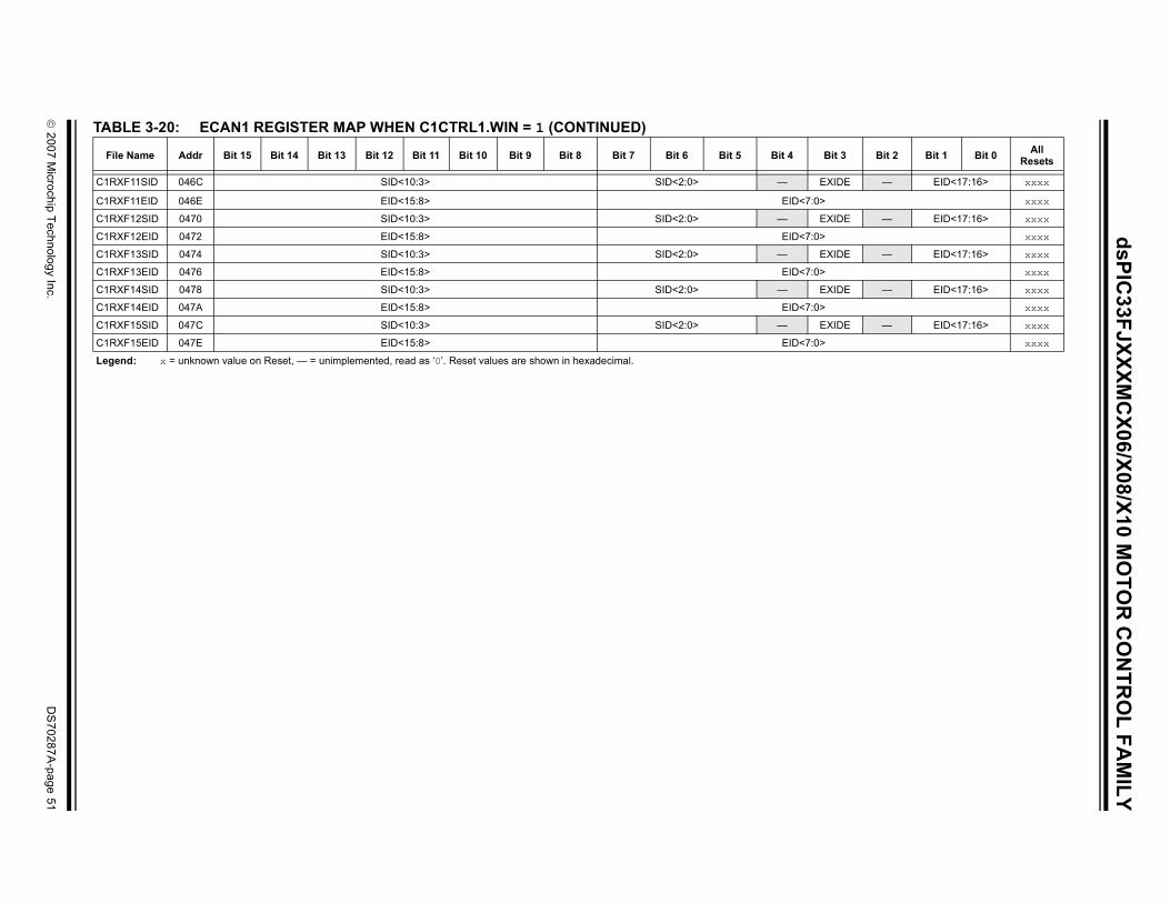
© 2007 M
icrochip Technology Inc.D
S70287A
-page 51
dsPIC33FJXXXM
CX06/X08/X10 M
OTO
R C
ON
TRO
L FAM
ILY
C1 XIDE — EID<17:16> xxxx
C1 xxxx
C1 XIDE — EID<17:16> xxxx
C1 xxxx
C1 XIDE — EID<17:16> xxxx
C1 xxxx
C1 XIDE — EID<17:16> xxxx
C1 xxxx
C1 XIDE — EID<17:16> xxxx
C1 xxxx
TA
F it 3 Bit 2 Bit 1 Bit 0 All Resets
Leg
RXF11SID 046C SID<10:3> SID<2:0> — E
RXF11EID 046E EID<15:8> EID<7:0>
RXF12SID 0470 SID<10:3> SID<2:0> — E
RXF12EID 0472 EID<15:8> EID<7:0>
RXF13SID 0474 SID<10:3> SID<2:0> — E
RXF13EID 0476 EID<15:8> EID<7:0>
RXF14SID 0478 SID<10:3> SID<2:0> — E
RXF14EID 047A EID<15:8> EID<7:0>
RXF15SID 047C SID<10:3> SID<2:0> — E
RXF15EID 047E EID<15:8> EID<7:0>
BLE 3-20: ECAN1 REGISTER MAP WHEN C1CTRL1.WIN = 1 (CONTINUED)
ile Name Addr Bit 15 Bit 14 Bit 13 Bit 12 Bit 11 Bit 10 Bit 9 Bit 8 Bit 7 Bit 6 Bit 5 Bit 4 B
end: x = unknown value on Reset, — = unimplemented, read as ‘0’. Reset values are shown in hexadecimal.
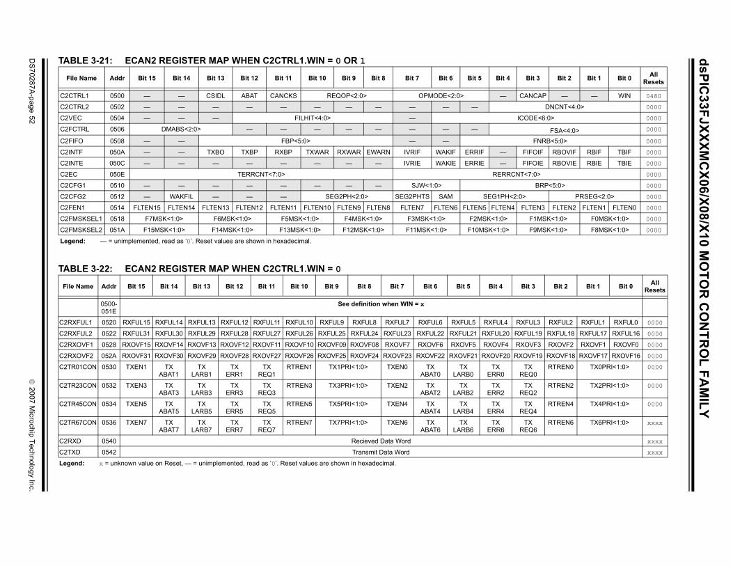
dsPIC33FJXXXM
CX06/X08/X10 M
OTO
R C
ON
TRO
L FAM
ILY
DS
70287A-page 52
© 2007 M
icrochip Technology Inc.
it 4 Bit 3 Bit 2 Bit 1 Bit 0 All Resets
CANCAP — — WIN 0480
DNCNT<4:0> 0000
ICODE<6:0> 0000
FSA<4:0> 0000
FNRB<5:0> 0000
FIFOIF RBOVIF RBIF TBIF 0000
FIFOIE RBOVIE RBIE TBIE 0000
RRCNT<7:0> 0000
BRP<5:0> 0000
PH<2:0> PRSEG<2:0> 0000
EN4 FLTEN3 FLTEN2 FLTEN1 FLTEN0 0000
0> F1MSK<1:0> F0MSK<1:0> 0000
:0> F9MSK<1:0> F8MSK<1:0> 0000
Bit 3 Bit 2 Bit 1 Bit 0 All Resets
L4 RXFUL3 RXFUL2 RXFUL1 RXFUL0 0000
20 RXFUL19 RXFUL18 RXFUL17 RXFUL16 0000
F4 RXOVF3 RXOVF2 RXOVF1 RXOVF0 0000
20 RXOVF19 RXOVF18 RXOVF17 RXOVF16 0000
0TX
REQ0RTREN0 TX0PRI<1:0> 0000
2TX
REQ2RTREN2 TX2PRI<1:0> 0000
4TX
REQ4RTREN4 TX4PRI<1:0> 0000
6TX
REQ6RTREN6 TX6PRI<1:0> xxxx
xxxx
xxxx
TABLE 3-21: ECAN2 REGISTER MAP WHEN C2CTRL1.WIN = 0 OR 1
File Name Addr Bit 15 Bit 14 Bit 13 Bit 12 Bit 11 Bit 10 Bit 9 Bit 8 Bit 7 Bit 6 Bit 5 B
C2CTRL1 0500 — — CSIDL ABAT CANCKS REQOP<2:0> OPMODE<2:0> —
C2CTRL2 0502 — — — — — — — — — — —
C2VEC 0504 — — — FILHIT<4:0> —
C2FCTRL 0506 DMABS<2:0> — — — — — — — —
C2FIFO 0508 — — FBP<5:0> — —
C2INTF 050A — — TXBO TXBP RXBP TXWAR RXWAR EWARN IVRIF WAKIF ERRIF —
C2INTE 050C — — — — — — — — IVRIE WAKIE ERRIE —
C2EC 050E TERRCNT<7:0> RE
C2CFG1 0510 — — — — — — — — SJW<1:0>
C2CFG2 0512 — WAKFIL — — — SEG2PH<2:0> SEG2PHTS SAM SEG1
C2FEN1 0514 FLTEN15 FLTEN14 FLTEN13 FLTEN12 FLTEN11 FLTEN10 FLTEN9 FLTEN8 FLTEN7 FLTEN6 FLTEN5 FLT
C2FMSKSEL1 0518 F7MSK<1:0> F6MSK<1:0> F5MSK<1:0> F4MSK<1:0> F3MSK<1:0> F2MSK<1:
C2FMSKSEL2 051A F15MSK<1:0> F14MSK<1:0> F13MSK<1:0> F12MSK<1:0> F11MSK<1:0> F10MSK<1
Legend: — = unimplemented, read as ‘0’. Reset values are shown in hexadecimal.
TABLE 3-22: ECAN2 REGISTER MAP WHEN C2CTRL1.WIN = 0
File Name Addr Bit 15 Bit 14 Bit 13 Bit 12 Bit 11 Bit 10 Bit 9 Bit 8 Bit 7 Bit 6 Bit 5 Bit 4
0500-051E
See definition when WIN = x
C2RXFUL1 0520 RXFUL15 RXFUL14 RXFUL13 RXFUL12 RXFUL11 RXFUL10 RXFUL9 RXFUL8 RXFUL7 RXFUL6 RXFUL5 RXFU
C2RXFUL2 0522 RXFUL31 RXFUL30 RXFUL29 RXFUL28 RXFUL27 RXFUL26 RXFUL25 RXFUL24 RXFUL23 RXFUL22 RXFUL21 RXFUL
C2RXOVF1 0528 RXOVF15 RXOVF14 RXOVF13 RXOVF12 RXOVF11 RXOVF10 RXOVF09 RXOVF08 RXOVF7 RXOVF6 RXOVF5 RXOV
C2RXOVF2 052A RXOVF31 RXOVF30 RXOVF29 RXOVF28 RXOVF27 RXOVF26 RXOVF25 RXOVF24 RXOVF23 RXOVF22 RXOVF21 RXOVF
C2TR01CON 0530 TXEN1 TXABAT1
TXLARB1
TXERR1
TXREQ1
RTREN1 TX1PRI<1:0> TXEN0 TXABAT0
TXLARB0
TXERR
C2TR23CON 0532 TXEN3 TXABAT3
TXLARB3
TXERR3
TXREQ3
RTREN3 TX3PRI<1:0> TXEN2 TXABAT2
TXLARB2
TXERR
C2TR45CON 0534 TXEN5 TXABAT5
TXLARB5
TXERR5
TXREQ5
RTREN5 TX5PRI<1:0> TXEN4 TXABAT4
TXLARB4
TXERR
C2TR67CON 0536 TXEN7 TXABAT7
TXLARB7
TXERR7
TXREQ7
RTREN7 TX7PRI<1:0> TXEN6 TXABAT6
TXLARB6
TXERR
C2RXD 0540 Recieved Data Word
C2TXD 0542 Transmit Data Word
Legend: x = unknown value on Reset, — = unimplemented, read as ‘0’. Reset values are shown in hexadecimal.
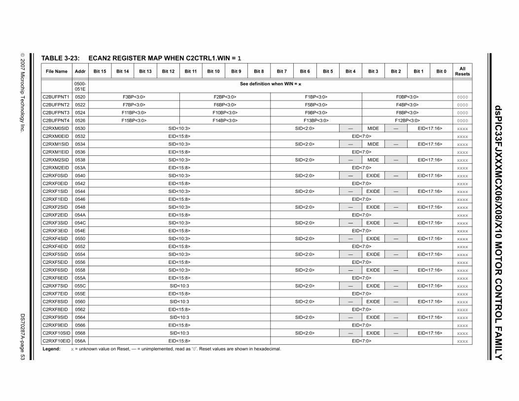
© 2007 M
icrochip Technology Inc.D
S70287A
-page 53
dsPIC33FJXXXM
CX06/X08/X10 M
OTO
R C
ON
TRO
L FAM
ILY
TA
F Bit 3 Bit 2 Bit 1 Bit 0 All Resets
C2 F0BP<3:0> 0000
C2 F4BP<3:0> 0000
C2 F8BP<3:0> 0000
C2 F12BP<3:0> 0000
C2 MIDE — EID<17:16> xxxx
C2 0> xxxx
C2 MIDE — EID<17:16> xxxx
C2 0> xxxx
C2 MIDE — EID<17:16> xxxx
C2 0> xxxx
C2 EXIDE — EID<17:16> xxxx
C2 0> xxxx
C2 EXIDE — EID<17:16> xxxx
C2 0> xxxx
C2 EXIDE — EID<17:16> xxxx
C2 0> xxxx
C2 EXIDE — EID<17:16> xxxx
C2 0> xxxx
C2 EXIDE — EID<17:16> xxxx
C2 0> xxxx
C2 EXIDE — EID<17:16> xxxx
C2 0> xxxx
C2 EXIDE — EID<17:16> xxxx
C2 0> xxxx
C2 EXIDE — EID<17:16> xxxx
C2 0> xxxx
C2 EXIDE — EID<17:16> xxxx
C2 0> xxxx
C2 EXIDE — EID<17:16> xxxx
C2 0> xxxx
C2 EXIDE — EID<17:16> xxxx
C2 0> xxxx
Le
BLE 3-23: ECAN2 REGISTER MAP WHEN C2CTRL1.WIN = 1
ile Name Addr Bit 15 Bit 14 Bit 13 Bit 12 Bit 11 Bit 10 Bit 9 Bit 8 Bit 7 Bit 6 Bit 5 Bit 4
0500-051E
See definition when WIN = x
BUFPNT1 0520 F3BP<3:0> F2BP<3:0> F1BP<3:0>
BUFPNT2 0522 F7BP<3:0> F6BP<3:0> F5BP<3:0>
BUFPNT3 0524 F11BP<3:0> F10BP<3:0> F9BP<3:0>
BUFPNT4 0526 F15BP<3:0> F14BP<3:0> F13BP<3:0>
RXM0SID 0530 SID<10:3> SID<2:0> —
RXM0EID 0532 EID<15:8> EID<7:
RXM1SID 0534 SID<10:3> SID<2:0> —
RXM1EID 0536 EID<15:8> EID<7:
RXM2SID 0538 SID<10:3> SID<2:0> —
RXM2EID 053A EID<15:8> EID<7:
RXF0SID 0540 SID<10:3> SID<2:0> —
RXF0EID 0542 EID<15:8> EID<7:
RXF1SID 0544 SID<10:3> SID<2:0> —
RXF1EID 0546 EID<15:8> EID<7:
RXF2SID 0548 SID<10:3> SID<2:0> —
RXF2EID 054A EID<15:8> EID<7:
RXF3SID 054C SID<10:3> SID<2:0> —
RXF3EID 054E EID<15:8> EID<7:
RXF4SID 0550 SID<10:3> SID<2:0> —
RXF4EID 0552 EID<15:8> EID<7:
RXF5SID 0554 SID<10:3> SID<2:0> —
RXF5EID 0556 EID<15:8> EID<7:
RXF6SID 0558 SID<10:3> SID<2:0> —
RXF6EID 055A EID<15:8> EID<7:
RXF7SID 055C SID<10:3 SID<2:0> —
RXF7EID 055E EID<15:8> EID<7:
RXF8SID 0560 SID<10:3 SID<2:0> —
RXF8EID 0562 EID<15:8> EID<7:
RXF9SID 0564 SID<10:3 SID<2:0> —
RXF9EID 0566 EID<15:8> EID<7:
RXF10SID 0568 SID<10:3 SID<2:0> —
RXF10EID 056A EID<15:8> EID<7:
gend: x = unknown value on Reset, — = unimplemented, read as ‘0’. Reset values are shown in hexadecimal.
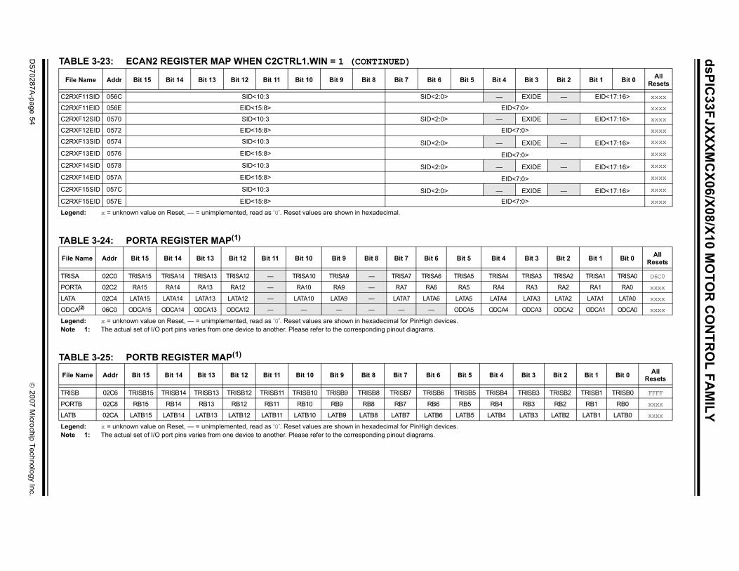
dsPIC33FJXXXM
CX06/X08/X10 M
OTO
R C
ON
TRO
L FAM
ILY
DS
70287A-page 54
© 2007 M
icrochip Technology Inc.
EXIDE — EID<17:16> xxxx
ID<7:0> xxxx
EXIDE — EID<17:16> xxxx
ID<7:0> xxxx
EXIDE — EID<17:16> xxxx
ID<7:0> xxxx
EXIDE — EID<17:16> xxxx
ID<7:0> xxxx
EXIDE — EID<17:16> xxxx
ID<7:0> xxxx
Bit 3 Bit 2 Bit 1 Bit 0 All Resets
Bit 3 Bit 2 Bit 1 Bit 0 All Resets
4 TRISA3 TRISA2 TRISA1 TRISA0 D6C0
RA3 RA2 RA1 RA0 xxxx
LATA3 LATA2 LATA1 LATA0 xxxx
4 ODCA3 ODCA2 ODCA1 ODCA0 xxxx
Bit 3 Bit 2 Bit 1 Bit 0 All Resets
TRISB3 TRISB2 TRISB1 TRISB0 FFFF
RB3 RB2 RB1 RB0 xxxx
LATB3 LATB2 LATB1 LATB0 xxxx
C2RXF11SID 056C SID<10:3 SID<2:0> —
C2RXF11EID 056E EID<15:8> E
C2RXF12SID 0570 SID<10:3 SID<2:0> —
C2RXF12EID 0572 EID<15:8> E
C2RXF13SID 0574 SID<10:3 SID<2:0> —C2RXF13EID 0576 EID<15:8> EC2RXF14SID 0578 SID<10:3 SID<2:0> —C2RXF14EID 057A EID<15:8> EC2RXF15SID 057C SID<10:3 SID<2:0> —C2RXF15EID 057E EID<15:8> E
TABLE 3-23: ECAN2 REGISTER MAP WHEN C2CTRL1.WIN = 1 (CONTINUED)
File Name Addr Bit 15 Bit 14 Bit 13 Bit 12 Bit 11 Bit 10 Bit 9 Bit 8 Bit 7 Bit 6 Bit 5 Bit 4
Legend: x = unknown value on Reset, — = unimplemented, read as ‘0’. Reset values are shown in hexadecimal.
TABLE 3-24: PORTA REGISTER MAP(1)
File Name Addr Bit 15 Bit 14 Bit 13 Bit 12 Bit 11 Bit 10 Bit 9 Bit 8 Bit 7 Bit 6 Bit 5 Bit 4
TRISA 02C0 TRISA15 TRISA14 TRISA13 TRISA12 — TRISA10 TRISA9 — TRISA7 TRISA6 TRISA5 TRISA
PORTA 02C2 RA15 RA14 RA13 RA12 — RA10 RA9 — RA7 RA6 RA5 RA4
LATA 02C4 LATA15 LATA14 LATA13 LATA12 — LATA10 LATA9 — LATA7 LATA6 LATA5 LATA4
ODCA(2) 06C0 ODCA15 ODCA14 ODCA13 ODCA12 — — — — — — ODCA5 ODCA
Legend: x = unknown value on Reset, — = unimplemented, read as ‘0’. Reset values are shown in hexadecimal for PinHigh devices.Note 1: The actual set of I/O port pins varies from one device to another. Please refer to the corresponding pinout diagrams.
TABLE 3-25: PORTB REGISTER MAP(1)
File Name Addr Bit 15 Bit 14 Bit 13 Bit 12 Bit 11 Bit 10 Bit 9 Bit 8 Bit 7 Bit 6 Bit 5 Bit 4
TRISB 02C6 TRISB15 TRISB14 TRISB13 TRISB12 TRISB11 TRISB10 TRISB9 TRISB8 TRISB7 TRISB6 TRISB5 TRISB4
PORTB 02C8 RB15 RB14 RB13 RB12 RB11 RB10 RB9 RB8 RB7 RB6 RB5 RB4
LATB 02CA LATB15 LATB14 LATB13 LATB12 LATB11 LATB10 LATB9 LATB8 LATB7 LATB6 LATB5 LATB4
Legend: x = unknown value on Reset, — = unimplemented, read as ‘0’. Reset values are shown in hexadecimal for PinHigh devices.Note 1: The actual set of I/O port pins varies from one device to another. Please refer to the corresponding pinout diagrams.
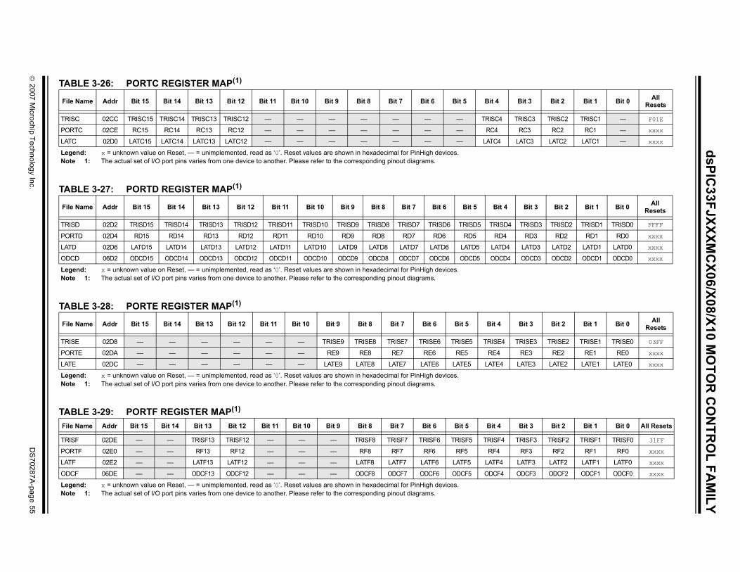
© 2007 M
icrochip Technology Inc.D
S70287A
-page 55
dsPIC33FJXXXM
CX06/X08/X10 M
OTO
R C
ON
TRO
L FAM
ILY
TA
Fil it 3 Bit 2 Bit 1 Bit 0 All Resets
TRI ISC3 TRISC2 TRISC1 — F01E
PO C3 RC2 RC1 — xxxx
LAT TC3 LATC2 LATC1 — xxxx
LegNo
TA
Fil Bit 3 Bit 2 Bit 1 Bit 0 All Resets
TRI RISD3 TRISD2 TRISD1 TRISD0 FFFF
PO RD3 RD2 RD1 RD0 xxxx
LAT ATD3 LATD2 LATD1 LATD0 xxxx
OD DCD3 ODCD2 ODCD1 ODCD0 xxxx
LegNo
TA
Fil it 3 Bit 2 Bit 1 Bit 0 All Resets
TRI ISE3 TRISE2 TRISE1 TRISE0 03FF
PO E3 RE2 RE1 RE0 xxxx
LAT TE3 LATE2 LATE1 LATE0 xxxx
LegNo
TAFil it 3 Bit 2 Bit 1 Bit 0 All Resets
TRI ISF3 TRISF2 TRISF1 TRISF0 31FF
PO F3 RF2 RF1 RF0 xxxx
LAT TF3 LATF2 LATF1 LATF0 xxxx
OD CF3 ODCF2 ODCF1 ODCF0 xxxx
LegNo
BLE 3-26: PORTC REGISTER MAP(1)
e Name Addr Bit 15 Bit 14 Bit 13 Bit 12 Bit 11 Bit 10 Bit 9 Bit 8 Bit 7 Bit 6 Bit 5 Bit 4 B
SC 02CC TRISC15 TRISC14 TRISC13 TRISC12 — — — — — — — TRISC4 TR
RTC 02CE RC15 RC14 RC13 RC12 — — — — — — — RC4 R
C 02D0 LATC15 LATC14 LATC13 LATC12 — — — — — — — LATC4 LA
end: x = unknown value on Reset, — = unimplemented, read as ‘0’. Reset values are shown in hexadecimal for PinHigh devices.te 1: The actual set of I/O port pins varies from one device to another. Please refer to the corresponding pinout diagrams.
BLE 3-27: PORTD REGISTER MAP(1)
e Name Addr Bit 15 Bit 14 Bit 13 Bit 12 Bit 11 Bit 10 Bit 9 Bit 8 Bit 7 Bit 6 Bit 5 Bit 4
SD 02D2 TRISD15 TRISD14 TRISD13 TRISD12 TRISD11 TRISD10 TRISD9 TRISD8 TRISD7 TRISD6 TRISD5 TRISD4 T
RTD 02D4 RD15 RD14 RD13 RD12 RD11 RD10 RD9 RD8 RD7 RD6 RD5 RD4
D 02D6 LATD15 LATD14 LATD13 LATD12 LATD11 LATD10 LATD9 LATD8 LATD7 LATD6 LATD5 LATD4 L
CD 06D2 ODCD15 ODCD14 ODCD13 ODCD12 ODCD11 ODCD10 ODCD9 ODCD8 ODCD7 ODCD6 ODCD5 ODCD4 O
end: x = unknown value on Reset, — = unimplemented, read as ‘0’. Reset values are shown in hexadecimal for PinHigh devices.te 1: The actual set of I/O port pins varies from one device to another. Please refer to the corresponding pinout diagrams.
BLE 3-28: PORTE REGISTER MAP(1)
e Name Addr Bit 15 Bit 14 Bit 13 Bit 12 Bit 11 Bit 10 Bit 9 Bit 8 Bit 7 Bit 6 Bit 5 Bit 4 B
SE 02D8 — — — — — — TRISE9 TRISE8 TRISE7 TRISE6 TRISE5 TRISE4 TR
RTE 02DA — — — — — — RE9 RE8 RE7 RE6 RE5 RE4 R
E 02DC — — — — — — LATE9 LATE8 LATE7 LATE6 LATE5 LATE4 LA
end: x = unknown value on Reset, — = unimplemented, read as ‘0’. Reset values are shown in hexadecimal for PinHigh devices.te 1: The actual set of I/O port pins varies from one device to another. Please refer to the corresponding pinout diagrams.
BLE 3-29: PORTF REGISTER MAP(1)
e Name Addr Bit 15 Bit 14 Bit 13 Bit 12 Bit 11 Bit 10 Bit 9 Bit 8 Bit 7 Bit 6 Bit 5 Bit 4 B
SF 02DE — — TRISF13 TRISF12 — — — TRISF8 TRISF7 TRISF6 TRISF5 TRISF4 TR
RTF 02E0 — — RF13 RF12 — — — RF8 RF7 RF6 RF5 RF4 R
F 02E2 — — LATF13 LATF12 — — — LATF8 LATF7 LATF6 LATF5 LATF4 LA
CF 06DE — — ODCF13 ODCF12 — — — ODCF8 ODCF7 ODCF6 ODCF5 ODCF4 OD
end: x = unknown value on Reset, — = unimplemented, read as ‘0’. Reset values are shown in hexadecimal for PinHigh devices.te 1: The actual set of I/O port pins varies from one device to another. Please refer to the corresponding pinout diagrams.
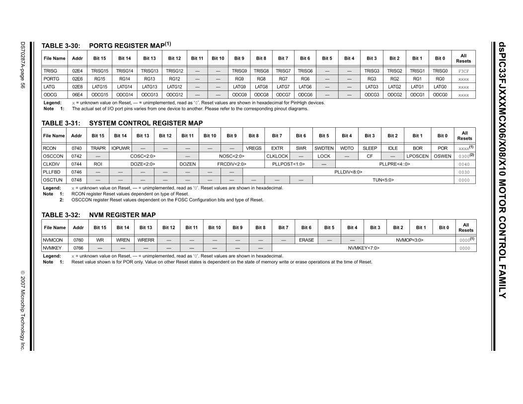
dsPIC33FJXXXM
CX06/X08/X10 M
OTO
R C
ON
TRO
L FAM
ILY
DS
70287A-page 56
© 2007 M
icrochip Technology Inc.
Bit 3 Bit 2 Bit 1 Bit 0 All Resets
TRISG3 TRISG2 TRISG1 TRISG0 F3CF
RG3 RG2 RG1 RG0 xxxx
LATG3 LATG2 LATG1 LATG0 xxxx
ODCG3 ODCG2 ODCG1 ODCG0 xxxx
Bit 3 Bit 2 Bit 1 Bit 0 All Resets
SLEEP IDLE BOR POR xxxx(1)
CF — LPOSCEN OSWEN 0300(2)
PLLPRE<4::0> 0040
0> 0030
TUN<5:0> 0000
Bit 3 Bit 2 Bit 1 Bit 0 All Resets
NVMOP<3:0> 0000(1)
KEY<7:0> 0000
Reset.
TABLE 3-30: PORTG REGISTER MAP(1)
File Name Addr Bit 15 Bit 14 Bit 13 Bit 12 Bit 11 Bit 10 Bit 9 Bit 8 Bit 7 Bit 6 Bit 5 Bit 4
TRISG 02E4 TRISG15 TRISG14 TRISG13 TRISG12 — — TRISG9 TRISG8 TRISG7 TRISG6 — —
PORTG 02E6 RG15 RG14 RG13 RG12 — — RG9 RG8 RG7 RG6 — —
LATG 02E8 LATG15 LATG14 LATG13 LATG12 — — LATG9 LATG8 LATG7 LATG6 — —
ODCG 06E4 ODCG15 ODCG14 ODCG13 ODCG12 — — ODCG9 ODCG8 ODCG7 ODCG6 — —
Legend: x = unknown value on Reset, — = unimplemented, read as ‘0’. Reset values are shown in hexadecimal for PinHigh devices.Note 1: The actual set of I/O port pins varies from one device to another. Please refer to the corresponding pinout diagrams.
TABLE 3-31: SYSTEM CONTROL REGISTER MAP
File Name Addr Bit 15 Bit 14 Bit 13 Bit 12 Bit 11 Bit 10 Bit 9 Bit 8 Bit 7 Bit 6 Bit 5 Bit 4
RCON 0740 TRAPR IOPUWR — — — — — VREGS EXTR SWR SWDTEN WDTO
OSCCON 0742 — COSC<2:0> — NOSC<2:0> CLKLOCK — LOCK —
CLKDIV 0744 ROI DOZE<2:0> DOZEN FRCDIV<2:0> PLLPOST<1:0> —
PLLFBD 0746 — — — — — — — PLLDIV<8:
OSCTUN 0748 — — — — — — — — — —
Legend: x = unknown value on Reset, — = unimplemented, read as ‘0’. Reset values are shown in hexadecimal.Note 1: RCON register Reset values dependent on type of Reset.
2: OSCCON register Reset values dependent on the FOSC Configuration bits and type of Reset.
TABLE 3-32: NVM REGISTER MAP
File Name Addr Bit 15 Bit 14 Bit 13 Bit 12 Bit 11 Bit 10 Bit 9 Bit 8 Bit 7 Bit 6 Bit 5 Bit 4
NVMCON 0760 WR WREN WRERR — — — — — — ERASE — —
NVMKEY 0766 — — — — — — — — NVM
Legend: x = unknown value on Reset, — = unimplemented, read as ‘0’. Reset values are shown in hexadecimal.Note 1: Reset value shown is for POR only. Value on other Reset states is dependent on the state of memory write or erase operations at the time of
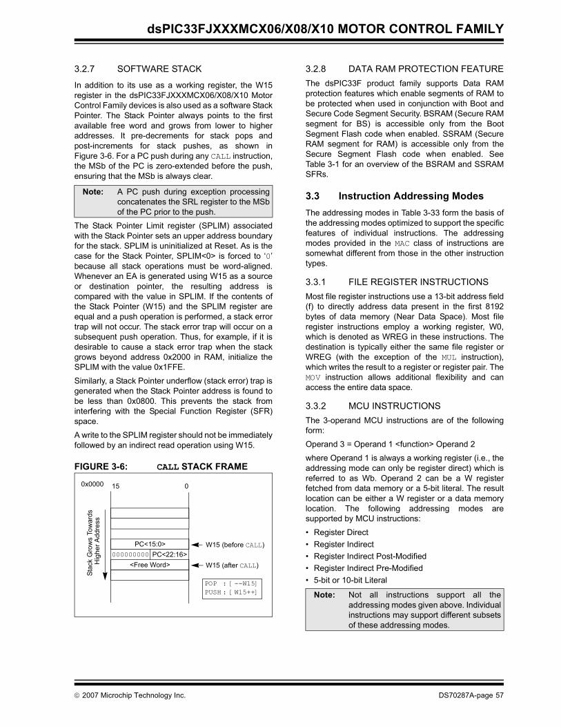
dsPIC33FJXXXMCX06/X08/X10 MOTOR CONTROL FAMILY
3.2.7 SOFTWARE STACK
In addition to its use as a working register, the W15register in the dsPIC33FJXXXMCX06/X08/X10 MotorControl Family devices is also used as a software StackPointer. The Stack Pointer always points to the firstavailable free word and grows from lower to higheraddresses. It pre-decrements for stack pops andpost-increments for stack pushes, as shown inFigure 3-6. For a PC push during any CALL instruction,the MSb of the PC is zero-extended before the push,ensuring that the MSb is always clear.
The Stack Pointer Limit register (SPLIM) associatedwith the Stack Pointer sets an upper address boundaryfor the stack. SPLIM is uninitialized at Reset. As is thecase for the Stack Pointer, SPLIM<0> is forced to ‘0’because all stack operations must be word-aligned.Whenever an EA is generated using W15 as a sourceor destination pointer, the resulting address iscompared with the value in SPLIM. If the contents ofthe Stack Pointer (W15) and the SPLIM register areequal and a push operation is performed, a stack errortrap will not occur. The stack error trap will occur on asubsequent push operation. Thus, for example, if it isdesirable to cause a stack error trap when the stackgrows beyond address 0x2000 in RAM, initialize theSPLIM with the value 0x1FFE.
Similarly, a Stack Pointer underflow (stack error) trap isgenerated when the Stack Pointer address is found tobe less than 0x0800. This prevents the stack frominterfering with the Special Function Register (SFR)space.
A write to the SPLIM register should not be immediatelyfollowed by an indirect read operation using W15.
FIGURE 3-6: CALL STACK FRAME
3.2.8 DATA RAM PROTECTION FEATUREThe dsPIC33F product family supports Data RAMprotection features which enable segments of RAM tobe protected when used in conjunction with Boot andSecure Code Segment Security. BSRAM (Secure RAMsegment for BS) is accessible only from the BootSegment Flash code when enabled. SSRAM (SecureRAM segment for RAM) is accessible only from theSecure Segment Flash code when enabled. SeeTable 3-1 for an overview of the BSRAM and SSRAMSFRs.
3.3 Instruction Addressing ModesThe addressing modes in Table 3-33 form the basis ofthe addressing modes optimized to support the specificfeatures of individual instructions. The addressingmodes provided in the MAC class of instructions aresomewhat different from those in the other instructiontypes.
3.3.1 FILE REGISTER INSTRUCTIONSMost file register instructions use a 13-bit address field(f) to directly address data present in the first 8192bytes of data memory (Near Data Space). Most fileregister instructions employ a working register, W0,which is denoted as WREG in these instructions. Thedestination is typically either the same file register orWREG (with the exception of the MUL instruction),which writes the result to a register or register pair. TheMOV instruction allows additional flexibility and canaccess the entire data space.
3.3.2 MCU INSTRUCTIONSThe 3-operand MCU instructions are of the followingform:
Operand 3 = Operand 1 <function> Operand 2
where Operand 1 is always a working register (i.e., theaddressing mode can only be register direct) which isreferred to as Wb. Operand 2 can be a W registerfetched from data memory or a 5-bit literal. The resultlocation can be either a W register or a data memorylocation. The following addressing modes aresupported by MCU instructions:
• Register Direct• Register Indirect• Register Indirect Post-Modified• Register Indirect Pre-Modified• 5-bit or 10-bit Literal
Note: A PC push during exception processingconcatenates the SRL register to the MSbof the PC prior to the push.
<Free Word>
PC<15:0>000000000
015
W15 (before CALL)
W15 (after CALL)
Stac
k G
row
s To
war
dsH
ighe
r Add
ress
0x0000
PC<22:16>
POP : [--W15]PUSH : [W15++] Note: Not all instructions support all the
addressing modes given above. Individualinstructions may support different subsetsof these addressing modes.
© 2007 Microchip Technology Inc. DS70287A-page 57
dsPIC33FJXXXMCX06/X08/X10 MOTOR CONTROL FAMILY
TABLE 3-33: FUNDAMENTAL ADDRESSING MODES SUPPORTED
3.3.3 MOVE AND ACCUMULATOR INSTRUCTIONS
Move instructions and the DSP accumulator class ofinstructions provide a greater degree of addressingflexibility than other instructions. In addition to theAddressing modes supported by most MCUinstructions, move and accumulator instructions alsosupport Register Indirect with Register OffsetAddressing mode, also referred to as Register Indexedmode.
In summary, the following Addressing modes aresupported by move and accumulator instructions:
• Register Direct• Register Indirect• Register Indirect Post-modified• Register Indirect Pre-modified• Register Indirect with Register Offset (Indexed)• Register Indirect with Literal Offset• 8-bit Literal• 16-bit Literal
3.3.4 MAC INSTRUCTIONSThe dual source operand DSP instructions (CLR, ED,EDAC, MAC, MPY, MPY.N, MOVSAC and MSC), also referredto as MAC instructions, utilize a simplified set ofaddressing modes to allow the user to effectivelymanipulate the data pointers through register indirecttables.
The 2-source operand prefetch registers must bemembers of the set {W8, W9, W10, W11}. For datareads, W8 and W9 are always directed to the X RAGUand W10 and W11 will always be directed to the YAGU. The effective addresses generated (before andafter modification) must, therefore, be valid addresseswithin X data space for W8 and W9 and Y data spacefor W10 and W11.
In summary, the following addressing modes aresupported by the MAC class of instructions:
• Register Indirect• Register Indirect Post-Modified by 2• Register Indirect Post-Modified by 4• Register Indirect Post-Modified by 6• Register Indirect with Register Offset (Indexed)
3.3.5 OTHER INSTRUCTIONSBesides the various addressing modes outlined above,some instructions use literal constants of various sizes.For example, BRA (branch) instructions use 16-bit signedliterals to specify the branch destination directly, whereasthe DISI instruction uses a 14-bit unsigned literal field. Insome instructions, such as ADD Acc, the source of anoperand or result is implied by the opcode itself. Certainoperations, such as NOP, do not have any operands.
3.4 Modulo AddressingModulo Addressing mode is a method of providing anautomated means to support circular data buffers usinghardware. The objective is to remove the need forsoftware to perform data address boundary checkswhen executing tightly looped code, as is typical inmany DSP algorithms.
Modulo Addressing can operate in either data or programspace (since the data pointer mechanism is essentiallythe same for both). One circular buffer can be supportedin each of the X (which also provides the pointers intoprogram space) and Y data spaces. Modulo Addressing
Addressing Mode Description
File Register Direct The address of the file register is specified explicitly.Register Direct The contents of a register are accessed directly.Register Indirect The contents of Wn forms the EA.Register Indirect Post-Modified The contents of Wn forms the EA. Wn is post-modified (incremented or
decremented) by a constant value.Register Indirect Pre-Modified Wn is pre-modified (incremented or decremented) by a signed constant value
to form the EA.Register Indirect with Register Offset The sum of Wn and Wb forms the EA.Register Indirect with Literal Offset The sum of Wn and a literal forms the EA.
Note: For the MOV instructions, the Addressingmode specified in the instruction can differfor the source and destination EA.However, the 4-bit Wb (Register Offset)field is shared between both source anddestination (but typically only used byone).
Note: Not all instructions support all theAddressing modes given above. Individualinstructions may support different subsetsof these Addressing modes.
Note: Register Indirect with Register OffsetAddressing mode is only available for W9(in X space) and W11 (in Y space).
DS70287A-page 58 © 2007 Microchip Technology Inc.
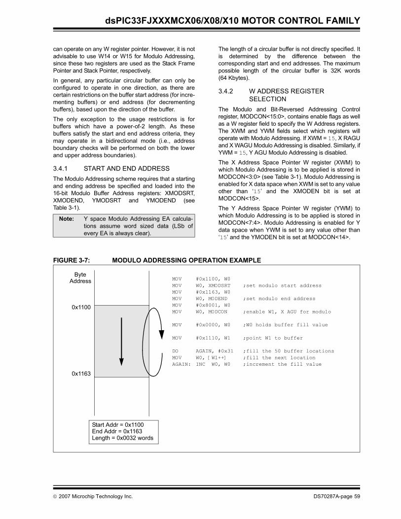
dsPIC33FJXXXMCX06/X08/X10 MOTOR CONTROL FAMILY
can operate on any W register pointer. However, it is notadvisable to use W14 or W15 for Modulo Addressing,since these two registers are used as the Stack FramePointer and Stack Pointer, respectively.
In general, any particular circular buffer can only beconfigured to operate in one direction, as there arecertain restrictions on the buffer start address (for incre-menting buffers) or end address (for decrementingbuffers), based upon the direction of the buffer.
The only exception to the usage restrictions is forbuffers which have a power-of-2 length. As thesebuffers satisfy the start and end address criteria, theymay operate in a bidirectional mode (i.e., addressboundary checks will be performed on both the lowerand upper address boundaries).
3.4.1 START AND END ADDRESSThe Modulo Addressing scheme requires that a startingand ending address be specified and loaded into the16-bit Modulo Buffer Address registers: XMODSRT,XMODEND, YMODSRT and YMODEND (seeTable 3-1).
The length of a circular buffer is not directly specified. Itis determined by the difference between thecorresponding start and end addresses. The maximumpossible length of the circular buffer is 32K words(64 Kbytes).
3.4.2 W ADDRESS REGISTER SELECTION
The Modulo and Bit-Reversed Addressing Controlregister, MODCON<15:0>, contains enable flags as wellas a W register field to specify the W Address registers.The XWM and YWM fields select which registers willoperate with Modulo Addressing. If XWM = 15, X RAGUand X WAGU Modulo Addressing is disabled. Similarly, ifYWM = 15, Y AGU Modulo Addressing is disabled.
The X Address Space Pointer W register (XWM) towhich Modulo Addressing is to be applied is stored inMODCON<3:0> (see Table 3-1). Modulo Addressing isenabled for X data space when XWM is set to any valueother than ‘15’ and the XMODEN bit is set atMODCON<15>.
The Y Address Space Pointer W register (YWM) towhich Modulo Addressing is to be applied is stored inMODCON<7:4>. Modulo Addressing is enabled for Ydata space when YWM is set to any value other than‘15’ and the YMODEN bit is set at MODCON<14>.
FIGURE 3-7: MODULO ADDRESSING OPERATION EXAMPLE
Note: Y space Modulo Addressing EA calcula-tions assume word sized data (LSb ofevery EA is always clear).
0x1100
0x1163
Start Addr = 0x1100End Addr = 0x1163Length = 0x0032 words
ByteAddress MOV #0x1100, W0
MOV W0, XMODSRT ;set modulo start addressMOV #0x1163, W0MOV W0, MODEND ;set modulo end addressMOV #0x8001, W0MOV W0, MODCON ;enable W1, X AGU for modulo
MOV #0x0000, W0 ;W0 holds buffer fill value
MOV #0x1110, W1 ;point W1 to buffer
DO AGAIN, #0x31 ;fill the 50 buffer locationsMOV W0, [W1++] ;fill the next locationAGAIN: INC W0, W0 ;increment the fill value
© 2007 Microchip Technology Inc. DS70287A-page 59
dsPIC33FJXXXMCX06/X08/X10 MOTOR CONTROL FAMILY
3.4.3 MODULO ADDRESSING APPLICABILITY
Modulo Addressing can be applied to the EffectiveAddress (EA) calculation associated with any Wregister. It is important to realize that the addressboundaries check for addresses less than or greaterthan the upper (for incrementing buffers) and lower (fordecrementing buffers) boundary addresses (not justequal to). Address changes may, therefore, jumpbeyond boundaries and still be adjusted correctly.
3.5 Bit-Reversed AddressingBit-Reversed Addressing mode is intended to simplifydata reordering for radix-2 FFT algorithms. It is supported by the X AGU for data writes only.
The modifier, which may be a constant value or registercontents, is regarded as having its bit order reversed. Theaddress source and destination are kept in normal order.Thus, the only operand requiring reversal is the modifier.
3.5.1 BIT-REVERSED ADDRESSING IMPLEMENTATION
Bit-Reversed Addressing mode is enabled when thefollowing conditions exist:
1. The BWM bits (W register selection) in theMODCON register are any value other than ‘15’(the stack cannot be accessed usingBit-Reversed Addressing).
2. The BREN bit is set in the XBREV register.3. The addressing mode used is Register Indirect
with Pre-Increment or Post-Increment.
If the length of a bit-reversed buffer is M = 2N bytes,the last ‘N’ bits of the data buffer start address mustbe zeros.
XB<14:0> is the Bit-Reversed Address modifier, or‘pivot point,’ which is typically a constant. In the case ofan FFT computation, its value is equal to half of the FFTdata buffer size.
When enabled, Bit-Reversed Addressing is only exe-cuted for Register Indirect with Pre-Increment orPost-Increment Addressing and word sized data writes.It will not function for any other addressing mode or forbyte sized data; normal addresses are generatedinstead. When Bit-Reversed Addressing is active, theW Address Pointer is always added to the addressmodifier (XB) and the offset associated with the Regis-ter Indirect Addressing mode is ignored. In addition, asword sized data is a requirement, the LSb of the EA isignored (and always clear).
If Bit-Reversed Addressing has already been enabledby setting the BREN (XBREV<15>) bit, then a write tothe XBREV register should not be immediately followedby an indirect read operation using the W register thathas been designated as the bit-reversed pointer.
Note: The modulo corrected effective address iswritten back to the register only whenPre-Modify or Post-Modify Addressingmode is used to compute the effectiveaddress. When an address offset (e.g.,[W7+W2]) is used, Modulo Address cor-rection is performed but the contents ofthe register remain unchanged.
Note: All bit-reversed EA calculations assumeword sized data (LSb of every EA isalways clear). The XB value is scaledaccordingly to generate compatible (byte)addresses.
Note: Modulo Addressing and Bit-ReversedAddressing should not be enabledtogether. In the event that the user attemptsto do so, Bit-Reversed Addressing willassume priority for the X WAGU, and XWAGU Modulo Addressing will be dis-abled. However, Modulo Addressing willcontinue to function in the X RAGU.
DS70287A-page 60 © 2007 Microchip Technology Inc.
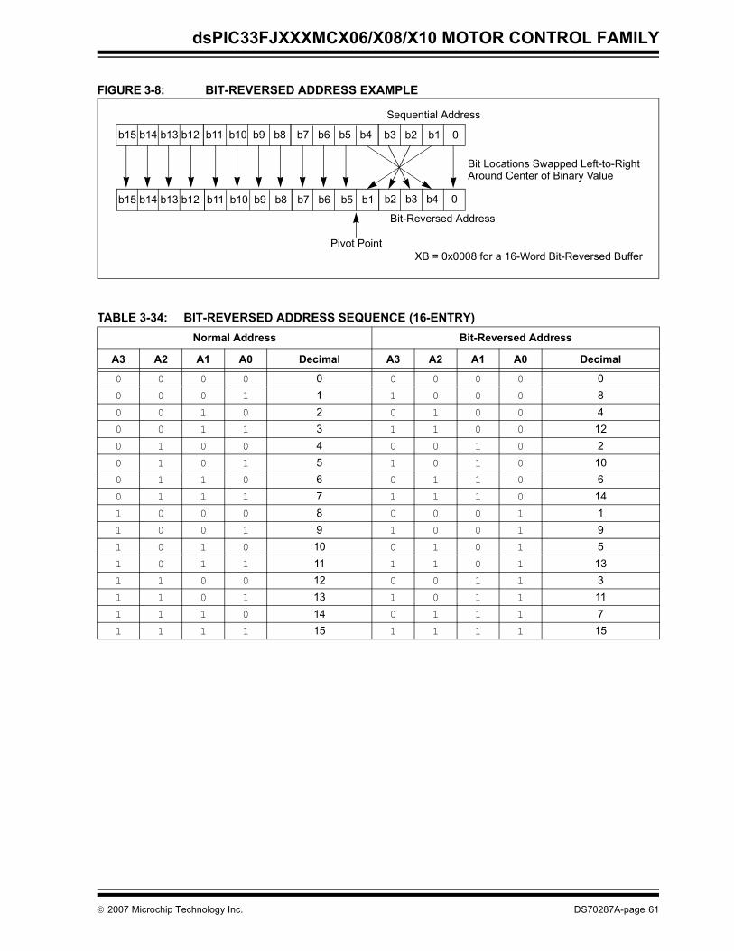
dsPIC33FJXXXMCX06/X08/X10 MOTOR CONTROL FAMILY
FIGURE 3-8: BIT-REVERSED ADDRESS EXAMPLE
TABLE 3-34: BIT-REVERSED ADDRESS SEQUENCE (16-ENTRY)
b3 b2 b1 0
b2 b3 b4 0
Bit Locations Swapped Left-to-RightAround Center of Binary Value
Bit-Reversed Address
XB = 0x0008 for a 16-Word Bit-Reversed Buffer
b7 b6 b5 b1
b7 b6 b5 b4b11 b10 b9 b8
b11 b10 b9 b8
b15 b14 b13 b12
b15 b14 b13 b12
Sequential Address
Pivot Point
Normal Address Bit-Reversed Address
A3 A2 A1 A0 Decimal A3 A2 A1 A0 Decimal
0 0 0 0 0 0 0 0 0 00 0 0 1 1 1 0 0 0 80 0 1 0 2 0 1 0 0 40 0 1 1 3 1 1 0 0 120 1 0 0 4 0 0 1 0 20 1 0 1 5 1 0 1 0 100 1 1 0 6 0 1 1 0 60 1 1 1 7 1 1 1 0 141 0 0 0 8 0 0 0 1 11 0 0 1 9 1 0 0 1 91 0 1 0 10 0 1 0 1 51 0 1 1 11 1 1 0 1 131 1 0 0 12 0 0 1 1 31 1 0 1 13 1 0 1 1 111 1 1 0 14 0 1 1 1 71 1 1 1 15 1 1 1 1 15
© 2007 Microchip Technology Inc. DS70287A-page 61
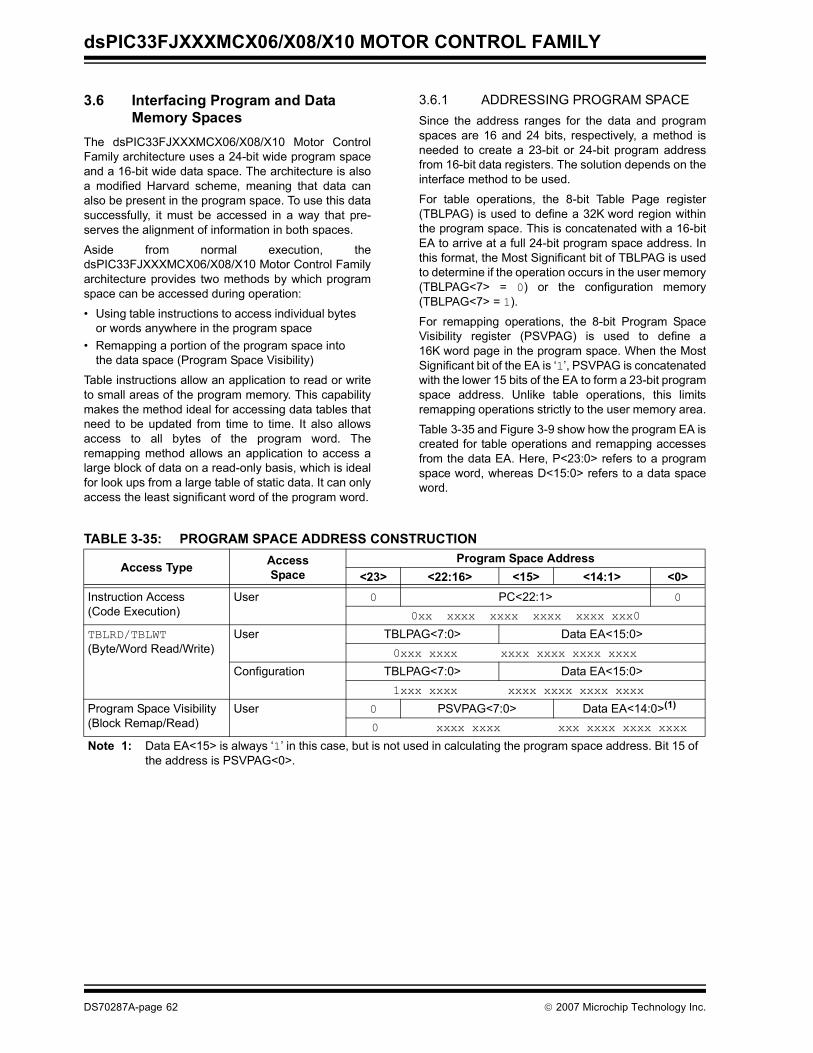
dsPIC33FJXXXMCX06/X08/X10 MOTOR CONTROL FAMILY
3.6 Interfacing Program and Data Memory Spaces
The dsPIC33FJXXXMCX06/X08/X10 Motor ControlFamily architecture uses a 24-bit wide program spaceand a 16-bit wide data space. The architecture is alsoa modified Harvard scheme, meaning that data canalso be present in the program space. To use this datasuccessfully, it must be accessed in a way that pre-serves the alignment of information in both spaces.
Aside from normal execution, thedsPIC33FJXXXMCX06/X08/X10 Motor Control Familyarchitecture provides two methods by which programspace can be accessed during operation:
• Using table instructions to access individual bytes or words anywhere in the program space
• Remapping a portion of the program space into the data space (Program Space Visibility)
Table instructions allow an application to read or writeto small areas of the program memory. This capabilitymakes the method ideal for accessing data tables thatneed to be updated from time to time. It also allowsaccess to all bytes of the program word. Theremapping method allows an application to access alarge block of data on a read-only basis, which is idealfor look ups from a large table of static data. It can onlyaccess the least significant word of the program word.
3.6.1 ADDRESSING PROGRAM SPACESince the address ranges for the data and programspaces are 16 and 24 bits, respectively, a method isneeded to create a 23-bit or 24-bit program addressfrom 16-bit data registers. The solution depends on theinterface method to be used.
For table operations, the 8-bit Table Page register(TBLPAG) is used to define a 32K word region withinthe program space. This is concatenated with a 16-bitEA to arrive at a full 24-bit program space address. Inthis format, the Most Significant bit of TBLPAG is usedto determine if the operation occurs in the user memory(TBLPAG<7> = 0) or the configuration memory(TBLPAG<7> = 1).
For remapping operations, the 8-bit Program SpaceVisibility register (PSVPAG) is used to define a16K word page in the program space. When the MostSignificant bit of the EA is ‘1’, PSVPAG is concatenatedwith the lower 15 bits of the EA to form a 23-bit programspace address. Unlike table operations, this limitsremapping operations strictly to the user memory area.
Table 3-35 and Figure 3-9 show how the program EA iscreated for table operations and remapping accessesfrom the data EA. Here, P<23:0> refers to a programspace word, whereas D<15:0> refers to a data spaceword.
TABLE 3-35: PROGRAM SPACE ADDRESS CONSTRUCTION
Access Type AccessSpace
Program Space Address<23> <22:16> <15> <14:1> <0>
Instruction Access(Code Execution)
User 0 PC<22:1> 0
0xx xxxx xxxx xxxx xxxx xxx0
TBLRD/TBLWT(Byte/Word Read/Write)
User TBLPAG<7:0> Data EA<15:0> 0xxx xxxx xxxx xxxx xxxx xxxx
Configuration TBLPAG<7:0> Data EA<15:0> 1xxx xxxx xxxx xxxx xxxx xxxx
Program Space Visibility(Block Remap/Read)
User 0 PSVPAG<7:0> Data EA<14:0>(1)
0 xxxx xxxx xxx xxxx xxxx xxxx
Note 1: Data EA<15> is always ‘1’ in this case, but is not used in calculating the program space address. Bit 15 of the address is PSVPAG<0>.
DS70287A-page 62 © 2007 Microchip Technology Inc.
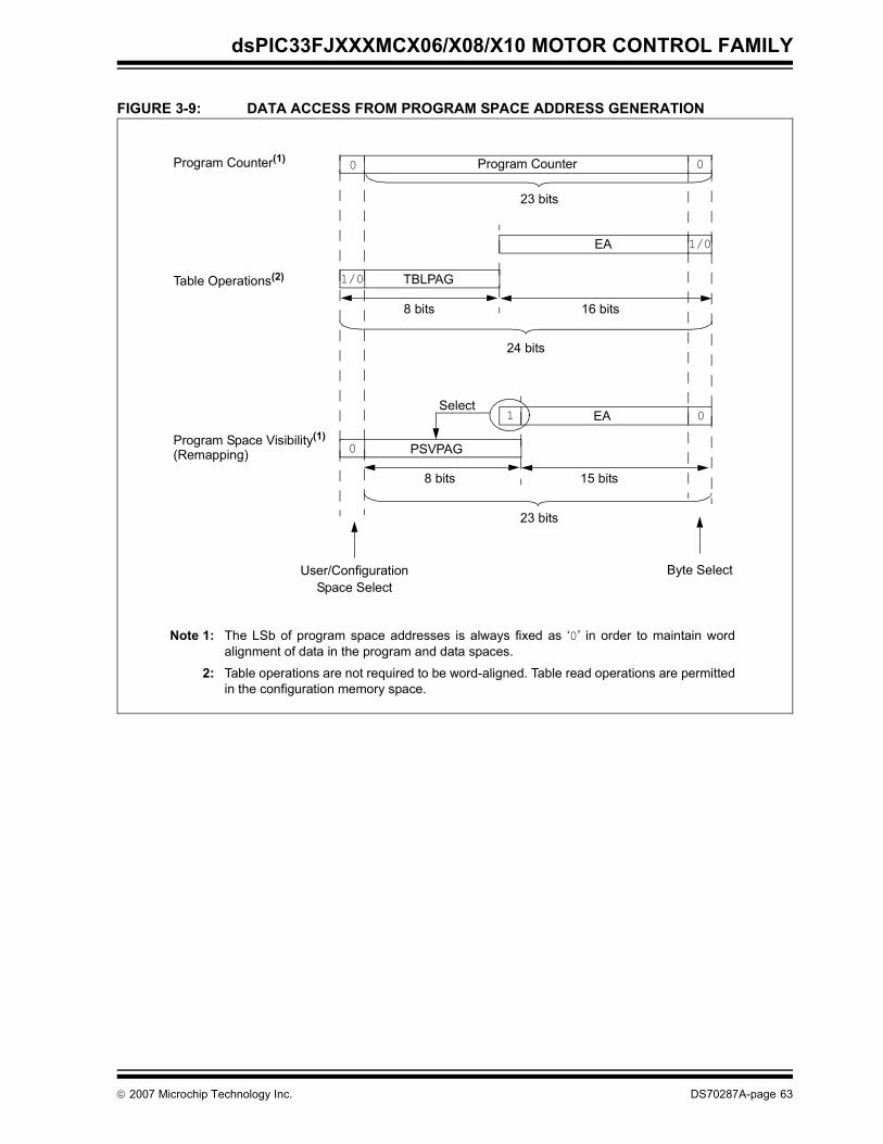
dsPIC33FJXXXMCX06/X08/X10 MOTOR CONTROL FAMILY
FIGURE 3-9: DATA ACCESS FROM PROGRAM SPACE ADDRESS GENERATION
0Program Counter
23 bits
1
PSVPAG
8 bits
EA
15 bits
Program Counter(1)
Select
TBLPAG
8 bits
EA
16 bits
Byte Select
0
0
1/0
User/Configuration
Table Operations(2)
Program Space Visibility(1)
Space Select
24 bits
23 bits
(Remapping)
1/0
0
Note 1: The LSb of program space addresses is always fixed as ‘0’ in order to maintain wordalignment of data in the program and data spaces.
2: Table operations are not required to be word-aligned. Table read operations are permittedin the configuration memory space.
© 2007 Microchip Technology Inc. DS70287A-page 63
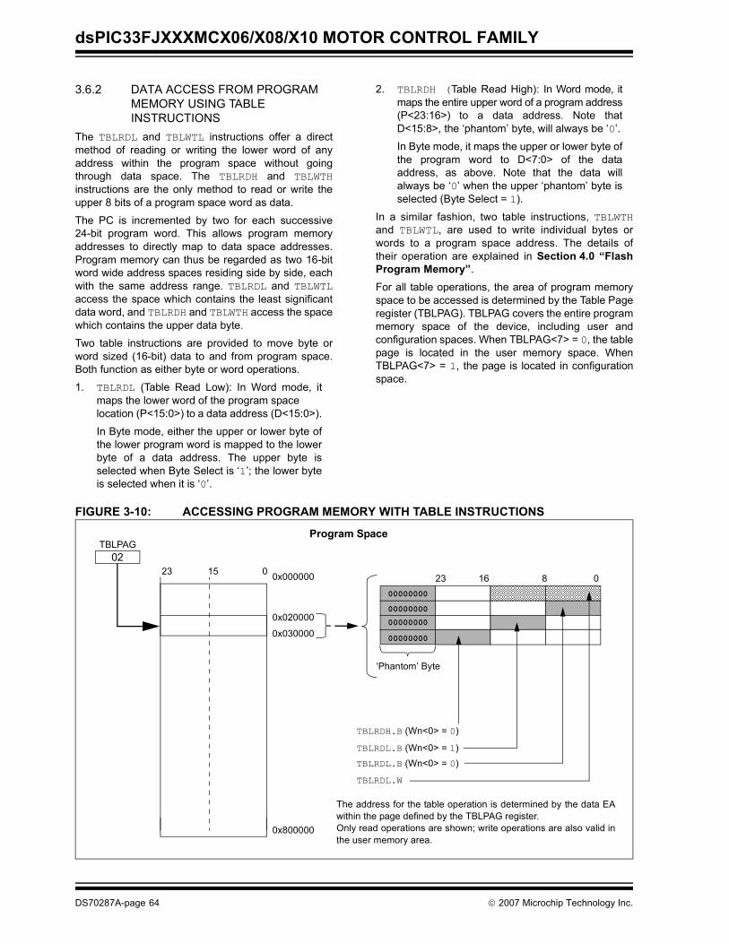
dsPIC33FJXXXMCX06/X08/X10 MOTOR CONTROL FAMILY
3.6.2 DATA ACCESS FROM PROGRAM MEMORY USING TABLE INSTRUCTIONS
The TBLRDL and TBLWTL instructions offer a directmethod of reading or writing the lower word of anyaddress within the program space without goingthrough data space. The TBLRDH and TBLWTHinstructions are the only method to read or write theupper 8 bits of a program space word as data.
The PC is incremented by two for each successive24-bit program word. This allows program memoryaddresses to directly map to data space addresses.Program memory can thus be regarded as two 16-bitword wide address spaces residing side by side, eachwith the same address range. TBLRDL and TBLWTLaccess the space which contains the least significantdata word, and TBLRDH and TBLWTH access the spacewhich contains the upper data byte.
Two table instructions are provided to move byte orword sized (16-bit) data to and from program space.Both function as either byte or word operations.
1. TBLRDL (Table Read Low): In Word mode, itmaps the lower word of the program space location (P<15:0>) to a data address (D<15:0>).
In Byte mode, either the upper or lower byte ofthe lower program word is mapped to the lowerbyte of a data address. The upper byte isselected when Byte Select is ‘1’; the lower byteis selected when it is ‘0’.
2. TBLRDH (Table Read High): In Word mode, itmaps the entire upper word of a program address(P<23:16>) to a data address. Note thatD<15:8>, the ‘phantom’ byte, will always be ‘0’.
In Byte mode, it maps the upper or lower byte ofthe program word to D<7:0> of the dataaddress, as above. Note that the data willalways be ‘0’ when the upper ‘phantom’ byte isselected (Byte Select = 1).
In a similar fashion, two table instructions, TBLWTHand TBLWTL, are used to write individual bytes orwords to a program space address. The details oftheir operation are explained in Section 4.0 “FlashProgram Memory”.
For all table operations, the area of program memoryspace to be accessed is determined by the Table Pageregister (TBLPAG). TBLPAG covers the entire programmemory space of the device, including user andconfiguration spaces. When TBLPAG<7> = 0, the tablepage is located in the user memory space. WhenTBLPAG<7> = 1, the page is located in configurationspace.
FIGURE 3-10: ACCESSING PROGRAM MEMORY WITH TABLE INSTRUCTIONS
08162300000000
00000000
00000000
00000000
‘Phantom’ Byte
TBLRDH.B (Wn<0> = 0)
TBLRDL.W
TBLRDL.B (Wn<0> = 1)TBLRDL.B (Wn<0> = 0)
23 15 0
TBLPAG02
0x000000
0x800000
0x020000
0x030000
Program Space
The address for the table operation is determined by the data EAwithin the page defined by the TBLPAG register. Only read operations are shown; write operations are also valid inthe user memory area.
DS70287A-page 64 © 2007 Microchip Technology Inc.
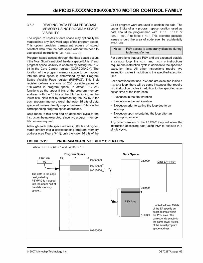
dsPIC33FJXXXMCX06/X08/X10 MOTOR CONTROL FAMILY
3.6.3 READING DATA FROM PROGRAM MEMORY USING PROGRAM SPACE VISIBILITY
The upper 32 Kbytes of data space may optionally bemapped into any 16K word page of the program space.This option provides transparent access of storedconstant data from the data space without the need touse special instructions (i.e., TBLRDL/H).
Program space access through the data space occursif the Most Significant bit of the data space EA is ‘1’ andprogram space visibility is enabled by setting the PSVbit in the Core Control register (CORCON<2>). Thelocation of the program memory space to be mappedinto the data space is determined by the ProgramSpace Visibility Page register (PSVPAG). This 8-bitregister defines any one of 256 possible pages of16K words in program space. In effect, PSVPAGfunctions as the upper 8 bits of the program memoryaddress, with the 15 bits of the EA functioning as thelower bits. Note that by incrementing the PC by 2 foreach program memory word, the lower 15 bits of dataspace addresses directly map to the lower 15 bits in thecorresponding program space addresses.
Data reads to this area add an additional cycle to theinstruction being executed, since two program memoryfetches are required.
Although each data space address, 8000h and higher,maps directly into a corresponding program memoryaddress (see Figure 3-11), only the lower 16 bits of the
24-bit program word are used to contain the data. Theupper 8 bits of any program space location used asdata should be programmed with ‘1111 1111’ or‘0000 0000’ to force a NOP. This prevents possibleissues should the area of code ever be accidentallyexecuted.
For operations that use PSV and are executed outsidea REPEAT loop, the MOV and MOV.D instructionsrequire one instruction cycle in addition to the specifiedexecution time. All other instructions require twoinstruction cycles in addition to the specified executiontime.
For operations that use PSV and are executed inside aREPEAT loop, there will be some instances that requiretwo instruction cycles in addition to the specified exe-cution time of the instruction:
• Execution in the first iteration• Execution in the last iteration• Execution prior to exiting the loop due to an
interrupt• Execution upon re-entering the loop after an
interrupt is serviced
Any other iteration of the REPEAT loop will allow theinstruction accessing data using PSV to execute in asingle cycle.
FIGURE 3-11: PROGRAM SPACE VISIBILITY OPERATION
Note: PSV access is temporarily disabled duringtable reads/writes.
23 15 0PSVPAGData SpaceProgram Space
0x0000
0x8000
0xFFFF
020x000000
0x800000
0x010000
0x018000
When CORCON<2> = 1 and EA<15> = 1:
The data in the page designated by PSVPAG is mapped into the upper half of the data memory space...
Data EA<14:0>
...while the lower 15 bits of the EA specify an exact address within the PSV area. This corresponds exactly to the same lower 15 bits of the actual program space address.
PSV Area
© 2007 Microchip Technology Inc. DS70287A-page 65

dsPIC33FJXXXMCX06/X08/X10 MOTOR CONTROL FAMILY
NOTES:
DS70287A-page 66 © 2007 Microchip Technology Inc.
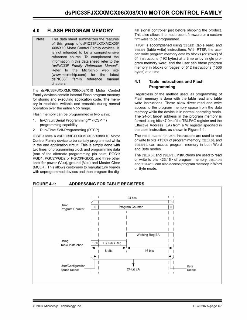
dsPIC33FJXXXMCX06/X08/X10 MOTOR CONTROL FAMILY
4.0 FLASH PROGRAM MEMORY
The dsPIC33FJXXXMCX06/X08/X10 Motor ControlFamily devices contain internal Flash program memoryfor storing and executing application code. The mem-ory is readable, writable and erasable during normaloperation over the entire VDD range.
Flash memory can be programmed in two ways:
1. In-Circuit Serial Programming™ (ICSP™) programming capability
2. Run-Time Self-Programming (RTSP)
ICSP allows a dsPIC33FJXXXMCX06/X08/X10 MotorControl Family device to be serially programmed whilein the end application circuit. This is simply done withtwo lines for programming clock and programming data(one of the alternate programming pin pairs: PGC1/PGD1, PGC2/PGD2 or PGC3/PGD3), and three otherlines for power (VDD), ground (VSS) and Master Clear(MCLR). This allows customers to manufacture boardswith unprogrammed devices and then program the dig-
ital signal controller just before shipping the product.This also allows the most recent firmware or a customfirmware to be programmed.
RTSP is accomplished using TBLRD (table read) andTBLWT (table write) instructions. With RTSP, the usercan write program memory data by blocks (or ‘rows’) of64 instructions (192 bytes) at a time or by single pro-gram memory word; and the user can erase programmemory in blocks or ‘pages’ of 512 instructions (1536bytes) at a time.
4.1 Table Instructions and Flash Programming
Regardless of the method used, all programming ofFlash memory is done with the table read and tablewrite instructions. These allow direct read and writeaccess to the program memory space from the datamemory while the device is in normal operating mode.The 24-bit target address in the program memory isformed using bits <7:0> of the TBLPAG register and theEffective Address (EA) from a W register specified inthe table instruction, as shown in Figure 4-1.
The TBLRDL and TBLWTL instructions are used to reador write to bits <15:0> of program memory. TBLRDL andTBLWTL can access program memory in both Wordand Byte modes.
The TBLRDH and TBLWTH instructions are used to reador write to bits <23:16> of program memory. TBLRDHand TBLWTH can also access program memory in Wordor Byte mode.
FIGURE 4-1: ADDRESSING FOR TABLE REGISTERS
Note: This data sheet summarizes the featuresof this group of dsPIC33FJXXXMCX06/X08/X10 Motor Control Family devices. Itis not intended to be a comprehensivereference source. To complement theinformation in this data sheet, refer to the“dsPIC33F Family Reference Manual”.Refer to the Microchip web site(www.microchip.com) for the latestdsPIC33F family reference manualchapters.
0Program Counter
24 bits
Program Counter
TBLPAG Reg
8 bits
Working Reg EA
16 bits
Byte24-bit EA
0
1/0
Select
UsingTable Instruction
Using
User/ConfigurationSpace Select
© 2007 Microchip Technology Inc. DS70287A-page 67
dsPIC33FJXXXMCX06/X08/X10 MOTOR CONTROL FAMILY
4.2 RTSP OperationThe dsPIC33FJXXXMCX06/X08/X10 Motor ControlFamily Flash program memory array is organized intorows of 64 instructions or 192 bytes. RTSP allows theuser to erase a page of memory at a time, which con-sists of eight rows (512 instructions), and to programone row or one word at a time. Table 25-12 shows typ-ical erase and programming times. The 8-row erasepages and single-row write rows are edge-aligned,from the beginning of program memory, on boundariesof 1536 bytes and 192 bytes, respectively.
The program memory implements holding buffers thatcan contain 64 instructions of programming data. Priorto the actual programming operation, the write datamust be loaded into the buffers in sequential order. Theinstruction words loaded must always be from a groupof 64 boundary.
The basic sequence for RTSP programming is to set upa Table Pointer, then do a series of TBLWT instructionsto load the buffers. Programming is performed bysetting the control bits in the NVMCON register. A totalof 64 TBLWTL and TBLWTH instructions are requiredto load the instructions.
All of the table write operations are single-word writes(two instruction cycles), because only the buffers arewritten. A programming cycle is required forprogramming each row.
4.3 Control RegistersThere are two SFRs used to read and write theprogram Flash memory: NVMCON and NVMKEY.
The NVMCON register (Register 4-1) controls whichblocks are to be erased, which memory type is to beprogrammed and the start of the programming cycle.
NVMKEY is a write-only register that is used for writeprotection. To start a programming or erase sequence,the user must consecutively write 55h and AAh to theNVMKEY register. Refer to Section 4.4 for furtherdetails.
4.4 Programming OperationsA complete programming sequence is necessary forprogramming or erasing the internal Flash in RTSPmode. A programming operation is nominally 4 ms induration, and the processor stalls (waits) until theoperation is finished. Setting the WR bit(NVMCON<15>) starts the operation; the WR bit isautomatically cleared when the operation is finished.
DS70287A-page 68 © 2007 Microchip Technology Inc.
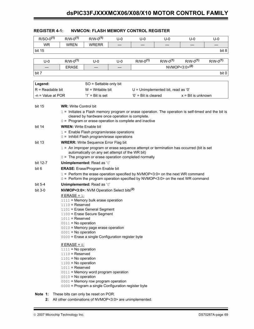
dsPIC33FJXXXMCX06/X08/X10 MOTOR CONTROL FAMILY
REGISTER 4-1: NVMCON: FLASH MEMORY CONTROL REGISTER
R/SO-0(1) R/W-0(1) R/W-0(1) U-0 U-0 U-0 U-0 U-0WR WREN WRERR — — — — —
bit 15 bit 8
U-0 R/W-0(1) U-0 U-0 R/W-0(1) R/W-0(1) R/W-0(1) R/W-0(1)
— ERASE — — NVMOP<3:0>(2)
bit 7 bit 0
Legend: SO = Settable only bitR = Readable bit W = Writable bit U = Unimplemented bit, read as ‘0’-n = Value at POR ‘1’ = Bit is set ‘0’ = Bit is cleared x = Bit is unknown
bit 15 WR: Write Control bit1 = Initiates a Flash memory program or erase operation. The operation is self-timed and the bit is
cleared by hardware once operation is complete. 0 = Program or erase operation is complete and inactive
bit 14 WREN: Write Enable bit1 = Enable Flash program/erase operations0 = Inhibit Flash program/erase operations
bit 13 WRERR: Write Sequence Error Flag bit1 = An improper program or erase sequence attempt or termination has occurred (bit is set
automatically on any set attempt of the WR bit)0 = The program or erase operation completed normally
bit 12-7 Unimplemented: Read as ‘0’bit 6 ERASE: Erase/Program Enable bit
1 = Perform the erase operation specified by NVMOP<3:0> on the next WR command0 = Perform the program operation specified by NVMOP<3:0> on the next WR command
bit 5-4 Unimplemented: Read as ‘0’bit 3-0 NVMOP<3:0>: NVM Operation Select bits(2)
If ERASE = 1:1111 = Memory bulk erase operation1110 = Reserved1101 = Erase General Segment1100 = Erase Secure Segment1011 = Reserved0011 = No operation0010 = Memory page erase operation0001 = No operation0000 = Erase a single Configuration register byte
If ERASE = 0:1111 = No operation1110 = Reserved1101 = No operation1100 = No operation1011 = Reserved0011 = Memory word program operation0010 = No operation0001 = Memory row program operation0000 = Program a single Configuration register byte
Note 1: These bits can only be reset on POR.2: All other combinations of NVMOP<3:0> are unimplemented.
© 2007 Microchip Technology Inc. DS70287A-page 69
dsPIC33FJXXXMCX06/X08/X10 MOTOR CONTROL FAMILY
4.4.1 PROGRAMMING ALGORITHM FOR FLASH PROGRAM MEMORY
The user can program one row of program Flashmemory at a time. To do this, it is necessary to erasethe 8-row erase page that contains the desired row.The general process is as follows:
1. Read eight rows of program memory(512 instructions) and store it in data RAM.
2. Update the program data in RAM with thedesired new data.
3. Erase the block (see Example 4-1):a) Set the NVMOP bits (NVMCON<3:0>) to
‘0010’ to configure for block erase. Set theERASE (NVMCON<6>) and WREN (NVM-CON<14>) bits.
b) Write the starting address of the page to beerased into the TBLPAG and W registers.
c) Write 55h to NVMKEY.d) Write AAh to NVMKEY.e) Set the WR bit (NVMCON<15>). The erase
cycle begins and the CPU stalls for the dura-tion of the erase cycle. When the erase isdone, the WR bit is cleared automatically.
4. Write the first 64 instructions from data RAM intothe program memory buffers (see Example 4-2).
5. Write the program block to Flash memory:a) Set the NVMOP bits to ‘0001’ to configure
for row programming. Clear the ERASE bitand set the WREN bit.
b) Write #0x55 to NVMKEY.c) Write 0xAA to NVMKEY.d) Set the WR bit. The programming cycle
begins and the CPU stalls for the duration ofthe write cycle. When the write to Flash mem-ory is done, the WR bit is clearedautomatically.
6. Repeat steps 4 and 5 using the next available 64instructions from the block in data RAM by incre-menting the value in TBLPAG until all512 instructions are written back to Flash memory.
For protection against accidental operations, the writeinitiate sequence for NVMKEY must be used to allowany erase or program operation to proceed. After theprogramming command has been executed, the usermust wait for the programming time until programmingis complete. The two instructions following the start ofthe programming sequence should be NOPs, as shownin Example 4-3.
EXAMPLE 4-1: ERASING A PROGRAM MEMORY PAGE ; Set up NVMCON for block erase operation
MOV #0x4042, W0 ;MOV W0, NVMCON ; Initialize NVMCON
; Init pointer to row to be ERASEDMOV #tblpage(PROG_ADDR), W0 ; MOV W0, TBLPAG ; Initialize PM Page Boundary SFRMOV #tbloffset(PROG_ADDR), W0 ; Initialize in-page EA[15:0] pointerTBLWTL W0, [W0] ; Set base address of erase blockDISI #5 ; Block all interrupts with priority <7
; for next 5 instructionsMOV #0x55, W0 MOV W0, NVMKEY ; Write the 55 key MOV #0xAA, W1 ;MOV W1, NVMKEY ; Write the AA keyBSET NVMCON, #WR ; Start the erase sequence NOP ; Insert two NOPs after the eraseNOP ; command is asserted
DS70287A-page 70 © 2007 Microchip Technology Inc.
dsPIC33FJXXXMCX06/X08/X10 MOTOR CONTROL FAMILY
EXAMPLE 4-2: LOADING THE WRITE BUFFERS
EXAMPLE 4-3: INITIATING A PROGRAMMING SEQUENCE
; Set up NVMCON for row programming operationsMOV #0x4001, W0 ;MOV W0, NVMCON ; Initialize NVMCON
; Set up a pointer to the first program memory location to be written; program memory selected, and writes enabled
MOV #0x0000, W0 ; MOV W0, TBLPAG ; Initialize PM Page Boundary SFRMOV #0x6000, W0 ; An example program memory address
; Perform the TBLWT instructions to write the latches; 0th_program_word
MOV #LOW_WORD_0, W2 ; MOV #HIGH_BYTE_0, W3 ; TBLWTL W2, [W0] ; Write PM low word into program latchTBLWTH W3, [W0++] ; Write PM high byte into program latch
; 1st_program_wordMOV #LOW_WORD_1, W2 ; MOV #HIGH_BYTE_1, W3 ; TBLWTL W2, [W0] ; Write PM low word into program latchTBLWTH W3, [W0++] ; Write PM high byte into program latch
; 2nd_program_wordMOV #LOW_WORD_2, W2 ; MOV #HIGH_BYTE_2, W3 ; TBLWTL W2, [W0] ; Write PM low word into program latchTBLWTH W3, [W0++] ; Write PM high byte into program latch•••
; 63rd_program_wordMOV #LOW_WORD_31, W2 ; MOV #HIGH_BYTE_31, W3 ; TBLWTL W2, [W0] ; Write PM low word into program latchTBLWTH W3, [W0++] ; Write PM high byte into program latch
DISI #5 ; Block all interrupts with priority <7; for next 5 instructions
MOV #0x55, W0MOV W0, NVMKEY ; Write the 55 key MOV #0xAA, W1 ;MOV W1, NVMKEY ; Write the AA keyBSET NVMCON, #WR ; Start the erase sequence NOP ; Insert two NOPs after theNOP ; erase command is asserted
© 2007 Microchip Technology Inc. DS70287A-page 71

dsPIC33FJXXXMCX06/X08/X10 MOTOR CONTROL FAMILY
NOTES:
DS70287A-page 72 © 2007 Microchip Technology Inc.
dsPIC33FJXXXMCX06/X08/X10 MOTOR CONTROL FAMILY
5.0 RESETS
The Reset module combines all Reset sources andcontrols the device Master Reset Signal, SYSRST. Thefollowing is a list of device Reset sources:
• POR: Power-on Reset • BOR: Brown-out Reset• MCLR: Master Clear Pin Reset• SWR: RESET Instruction• WDT: Watchdog Timer Reset• TRAPR: Trap Conflict Reset• IOPUWR: Illegal Opcode and Uninitialized W
Register Reset
A simplified block diagram of the Reset module isshown in Figure 5-1.
Any active source of Reset will make the SYSRSTsignal active. Many registers associated with the CPUand peripherals are forced to a known Reset state.Most registers are unaffected by a Reset; their status isunknown on POR and unchanged by all other Resets.
All types of device Reset will set a corresponding statusbit in the RCON register to indicate the type of Reset(see Register 5-1). A POR will clear all bits except forthe POR bit (RCON<0>), which is set. The user can setor clear any bit at any time during code execution. TheRCON bits only serve as status bits. Setting a particularReset status bit in software does not cause a deviceReset to occur.
The RCON register also has other bits associated withthe Watchdog Timer and device power-saving states.The function of these bits is discussed in other sectionsof this manual.
FIGURE 5-1: RESET SYSTEM BLOCK DIAGRAM
Note: This data sheet summarizes the featuresof this groupof dsPIC33FJXXXMCX06/X08/X10 MotorControl Family devices. It is not intendedto be a comprehensive reference source.To complement the information in this datasheet, refer to the “dsPIC33F FamilyReference Manual”. Refer to theMicrochip web site (www.microchip.com)for the latest dsPIC33F family referencemanual chapters.
Note: Refer to the specific peripheral or CPUsection of this manual for register Resetstates.
Note: The status bits in the RCON registershould be cleared after they are read sothat the next RCON register value after adevice Reset will be meaningful.
MCLR
VDD
InternalRegulator
BOR
Sleep or Idle
RESET Instruction
WDTModule
Glitch Filter
Trap Conflict
Illegal Opcode
Uninitialized W Register
SYSRST
VDD RiseDetect
POR
© 2007 Microchip Technology Inc. DS70287A-page 73
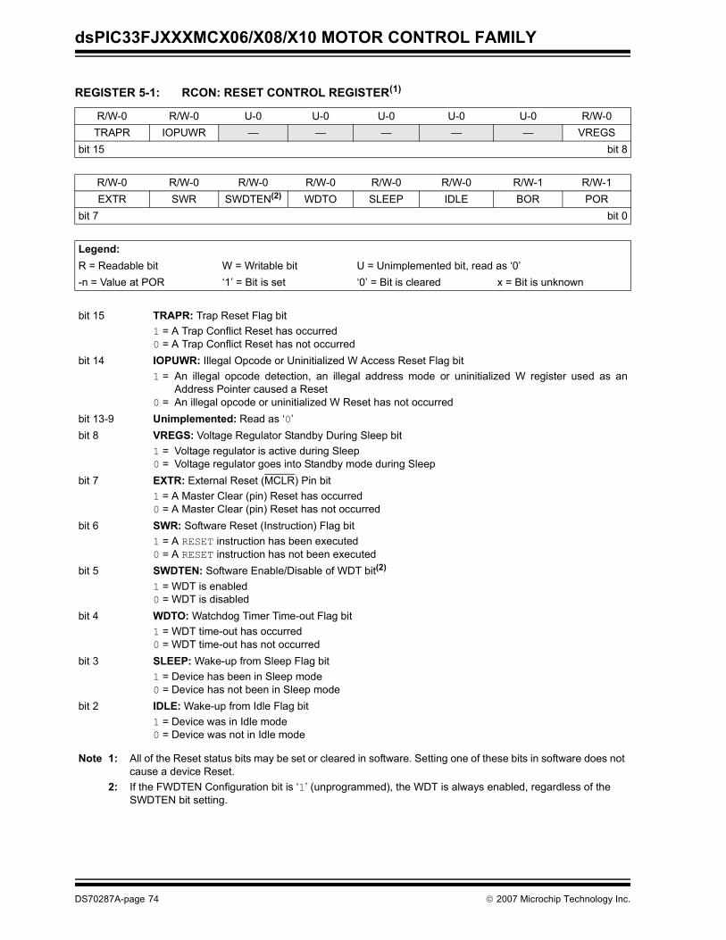
dsPIC33FJXXXMCX06/X08/X10 MOTOR CONTROL FAMILY
REGISTER 5-1: RCON: RESET CONTROL REGISTER(1)
R/W-0 R/W-0 U-0 U-0 U-0 U-0 U-0 R/W-0TRAPR IOPUWR — — — — — VREGS
bit 15 bit 8
R/W-0 R/W-0 R/W-0 R/W-0 R/W-0 R/W-0 R/W-1 R/W-1EXTR SWR SWDTEN(2) WDTO SLEEP IDLE BOR POR
bit 7 bit 0
Legend:R = Readable bit W = Writable bit U = Unimplemented bit, read as ‘0’-n = Value at POR ‘1’ = Bit is set ‘0’ = Bit is cleared x = Bit is unknown
bit 15 TRAPR: Trap Reset Flag bit1 = A Trap Conflict Reset has occurred0 = A Trap Conflict Reset has not occurred
bit 14 IOPUWR: Illegal Opcode or Uninitialized W Access Reset Flag bit1 = An illegal opcode detection, an illegal address mode or uninitialized W register used as an
Address Pointer caused a Reset0 = An illegal opcode or uninitialized W Reset has not occurred
bit 13-9 Unimplemented: Read as ‘0’bit 8 VREGS: Voltage Regulator Standby During Sleep bit
1 = Voltage regulator is active during Sleep0 = Voltage regulator goes into Standby mode during Sleep
bit 7 EXTR: External Reset (MCLR) Pin bit1 = A Master Clear (pin) Reset has occurred0 = A Master Clear (pin) Reset has not occurred
bit 6 SWR: Software Reset (Instruction) Flag bit1 = A RESET instruction has been executed0 = A RESET instruction has not been executed
bit 5 SWDTEN: Software Enable/Disable of WDT bit(2)
1 = WDT is enabled0 = WDT is disabled
bit 4 WDTO: Watchdog Timer Time-out Flag bit1 = WDT time-out has occurred0 = WDT time-out has not occurred
bit 3 SLEEP: Wake-up from Sleep Flag bit1 = Device has been in Sleep mode0 = Device has not been in Sleep mode
bit 2 IDLE: Wake-up from Idle Flag bit1 = Device was in Idle mode0 = Device was not in Idle mode
Note 1: All of the Reset status bits may be set or cleared in software. Setting one of these bits in software does not cause a device Reset.
2: If the FWDTEN Configuration bit is ‘1’ (unprogrammed), the WDT is always enabled, regardless of the SWDTEN bit setting.
DS70287A-page 74 © 2007 Microchip Technology Inc.
dsPIC33FJXXXMCX06/X08/X10 MOTOR CONTROL FAMILY
bit 1 BOR: Brown-out Reset Flag bit1 = A Brown-out Reset has occurred0 = A Brown-out Reset has not occurred
bit 0 POR: Power-on Reset Flag bit1 = A Power-up Reset has occurred0 = A Power-up Reset has not occurred
REGISTER 5-1: RCON: RESET CONTROL REGISTER(1) (CONTINUED)
Note 1: All of the Reset status bits may be set or cleared in software. Setting one of these bits in software does not cause a device Reset.
2: If the FWDTEN Configuration bit is ‘1’ (unprogrammed), the WDT is always enabled, regardless of the SWDTEN bit setting.
© 2007 Microchip Technology Inc. DS70287A-page 75
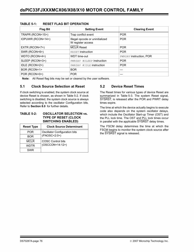
dsPIC33FJXXXMCX06/X08/X10 MOTOR CONTROL FAMILY
TABLE 5-1: RESET FLAG BIT OPERATION
5.1 Clock Source Selection at ResetIf clock switching is enabled, the system clock source atdevice Reset is chosen, as shown in Table 5-2. If clockswitching is disabled, the system clock source is alwaysselected according to the oscillator Configuration bits.Refer to Section 8.0 for further details.
TABLE 5-2: OSCILLATOR SELECTION vs. TYPE OF RESET (CLOCK SWITCHING ENABLED)
5.2 Device Reset TimesThe Reset times for various types of device Reset aresummarized in Table 5-3. The system Reset signal,SYSRST, is released after the POR and PWRT delaytimes expire.
The time at which the device actually begins to executecode also depends on the system oscillator delays,which include the Oscillator Start-up Timer (OST) andthe PLL lock time. The OST and PLL lock times occurin parallel with the applicable SYSRST delay times.
The FSCM delay determines the time at which theFSCM begins to monitor the system clock source afterthe SYSRST signal is released.
Flag Bit Setting Event Clearing Event
TRAPR (RCON<15>) Trap conflict event PORIOPUWR (RCON<14>) Illegal opcode or uninitialized
W register accessPOR
EXTR (RCON<7>) MCLR Reset PORSWR (RCON<6>) RESET instruction PORWDTO (RCON<4>) WDT time-out PWRSAV instruction, PORSLEEP (RCON<3>) PWRSAV #SLEEP instruction PORIDLE (RCON<2>) PWRSAV #IDLE instruction PORBOR (RCON<1> BOR —POR (RCON<0>) POR —Note: All Reset flag bits may be set or cleared by the user software.
Reset Type Clock Source Determinant
POR Oscillator Configuration bits(FNOSC<2:0>)BOR
MCLR COSC Control bits (OSCCON<14:12>)WDTR
SWR
DS70287A-page 76 © 2007 Microchip Technology Inc.
dsPIC33FJXXXMCX06/X08/X10 MOTOR CONTROL FAMILY
TABLE 5-3: RESET DELAY TIMES FOR VARIOUS DEVICE RESETS
5.2.1 POR AND LONG OSCILLATOR START-UP TIMES
The oscillator start-up circuitry and its associated delaytimers are not linked to the device Reset delays thatoccur at power-up. Some crystal circuits (especiallylow-frequency crystals) have a relatively long start-uptime. Therefore, one or more of the following conditionsis possible after SYSRST is released:
• The oscillator circuit has not begun to oscillate.• The Oscillator Start-up Timer has not expired (if a
crystal oscillator is used).• The PLL has not achieved a lock (if PLL is used).
The device will not begin to execute code until a validclock source has been released to the system.Therefore, the oscillator and PLL start-up delays mustbe considered when the Reset delay time must beknown.
5.2.2 FAIL-SAFE CLOCK MONITOR (FSCM) AND DEVICE RESETS
If the FSCM is enabled, it begins to monitor the systemclock source when SYSRST is released. If a valid clocksource is not available at this time, the deviceautomatically switches to the FRC oscillator and theuser can switch to the desired crystal oscillator in theTrap Service Routine.
5.2.2.1 FSCM Delay for Crystal and PLL Clock Sources
When the system clock source is provided by a crystaloscillator and/or the PLL, a small delay, TFSCM, isautomatically inserted after the POR and PWRT delaytimes. The FSCM does not begin to monitor the systemclock source until this delay expires. The FSCM delaytime is nominally 500 μs and provides additional timefor the oscillator and/or PLL to stabilize. In most cases,the FSCM delay prevents an oscillator failure trap at adevice Reset when the PWRT is disabled.
Reset Type Clock Source SYSRST Delay System ClockDelay
FSCMDelay Notes
POR EC, FRC, LPRC TPOR + TSTARTUP + TRST — — 1, 2, 3ECPLL, FRCPLL TPOR + TSTARTUP + TRST TLOCK TFSCM 1, 2, 3, 5, 6XT, HS, SOSC TPOR + TSTARTUP + TRST TOST TFSCM 1, 2, 3, 4, 6XTPLL, HSPLL TPOR + TSTARTUP + TRST TOST + TLOCK TFSCM 1, 2, 3, 4, 5, 6
BOR EC, FRC, LPRC TSTARTUP + TRST — — 3ECPLL, FRCPLL TSTARTUP + TRST TLOCK TFSCM 3, 5, 6XT, HS, SOSC TSTARTUP + TRST TOST TFSCM 3, 4, 6XTPLL, HSPLL TSTARTUP + TRST TOST + TLOCK TFSCM 3, 4, 5, 6
MCLR Any Clock TRST — — 3WDT Any Clock TRST — — 3Software Any Clock TRST — — 3Illegal Opcode Any Clock TRST — — 3Uninitialized W Any Clock TRST — — 3Trap Conflict Any Clock TRST — — 3Note 1: TPOR = Power-on Reset delay (10 μs nominal).
2: TSTARTUP = Conditional POR delay of 20 μs nominal (if on-chip regulator is enabled) or 64 ms nominal Power-up Timer delay (if regulator is disabled). TSTARTUP is also applied to all returns from powered-down states, including waking from Sleep mode, if the regulator is enabled.
3: TRST = Internal state Reset time (20 μs nominal).4: TOST = Oscillator Start-up Timer. A 10-bit counter counts 1024 oscillator periods before releasing the
oscillator clock to the system.5: TLOCK = PLL lock time (20 μs nominal).6: TFSCM = Fail-Safe Clock Monitor delay (100 μs nominal).
© 2007 Microchip Technology Inc. DS70287A-page 77
dsPIC33FJXXXMCX06/X08/X10 MOTOR CONTROL FAMILY
5.3 Special Function Register Reset States
Most of the Special Function Registers (SFRs)associated with the CPU and peripherals are reset to aparticular value at a device Reset. The SFRs aregrouped by their peripheral or CPU function, and theirReset values are specified in each section of this manual.
The Reset value for each SFR does not depend on thetype of Reset, with the exception of two registers. TheReset value for the Reset Control register, RCON,depends on the type of device Reset. The Reset valuefor the Oscillator Control register, OSCCON, dependson the type of Reset and the programmed values of theoscillator Configuration bits in the FOSC Configurationregister.
DS70287A-page 78 © 2007 Microchip Technology Inc.
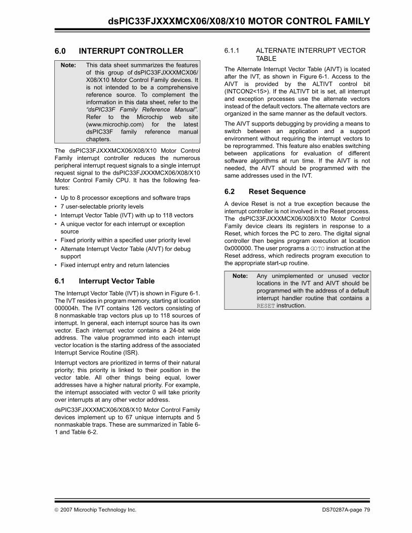
dsPIC33FJXXXMCX06/X08/X10 MOTOR CONTROL FAMILY
6.0 INTERRUPT CONTROLLER
The dsPIC33FJXXXMCX06/X08/X10 Motor ControlFamily interrupt controller reduces the numerousperipheral interrupt request signals to a single interruptrequest signal to the dsPIC33FJXXXMCX06/X08/X10Motor Control Family CPU. It has the following fea-tures:
• Up to 8 processor exceptions and software traps• 7 user-selectable priority levels• Interrupt Vector Table (IVT) with up to 118 vectors• A unique vector for each interrupt or exception
source• Fixed priority within a specified user priority level• Alternate Interrupt Vector Table (AIVT) for debug
support• Fixed interrupt entry and return latencies
6.1 Interrupt Vector TableThe Interrupt Vector Table (IVT) is shown in Figure 6-1.The IVT resides in program memory, starting at location000004h. The IVT contains 126 vectors consisting of8 nonmaskable trap vectors plus up to 118 sources ofinterrupt. In general, each interrupt source has its ownvector. Each interrupt vector contains a 24-bit wideaddress. The value programmed into each interruptvector location is the starting address of the associatedInterrupt Service Routine (ISR).
Interrupt vectors are prioritized in terms of their naturalpriority; this priority is linked to their position in thevector table. All other things being equal, loweraddresses have a higher natural priority. For example,the interrupt associated with vector 0 will take priorityover interrupts at any other vector address.
dsPIC33FJXXXMCX06/X08/X10 Motor Control Familydevices implement up to 67 unique interrupts and 5nonmaskable traps. These are summarized in Table 6-1 and Table 6-2.
6.1.1 ALTERNATE INTERRUPT VECTOR TABLE
The Alternate Interrupt Vector Table (AIVT) is locatedafter the IVT, as shown in Figure 6-1. Access to theAIVT is provided by the ALTIVT control bit(INTCON2<15>). If the ALTIVT bit is set, all interruptand exception processes use the alternate vectorsinstead of the default vectors. The alternate vectors areorganized in the same manner as the default vectors.
The AIVT supports debugging by providing a means toswitch between an application and a supportenvironment without requiring the interrupt vectors tobe reprogrammed. This feature also enables switchingbetween applications for evaluation of differentsoftware algorithms at run time. If the AIVT is notneeded, the AIVT should be programmed with thesame addresses used in the IVT.
6.2 Reset SequenceA device Reset is not a true exception because theinterrupt controller is not involved in the Reset process.The dsPIC33FJXXXMCX06/X08/X10 Motor ControlFamily device clears its registers in response to aReset, which forces the PC to zero. The digital signalcontroller then begins program execution at location0x000000. The user programs a GOTO instruction at theReset address, which redirects program execution tothe appropriate start-up routine.
Note: This data sheet summarizes the featuresof this group of dsPIC33FJXXXMCX06/X08/X10 Motor Control Family devices. Itis not intended to be a comprehensivereference source. To complement theinformation in this data sheet, refer to the“dsPIC33F Family Reference Manual”.Refer to the Microchip web site(www.microchip.com) for the latestdsPIC33F family reference manualchapters.
Note: Any unimplemented or unused vectorlocations in the IVT and AIVT should beprogrammed with the address of a defaultinterrupt handler routine that contains aRESET instruction.
© 2007 Microchip Technology Inc. DS70287A-page 79
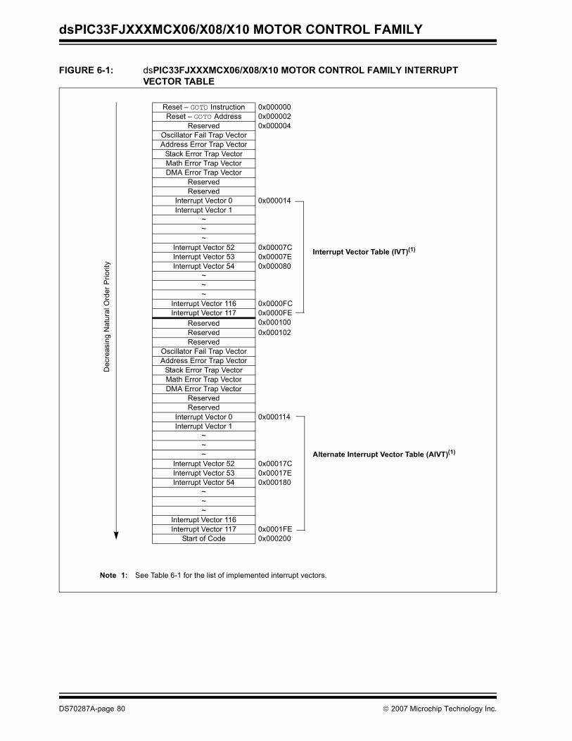
dsPIC33FJXXXMCX06/X08/X10 MOTOR CONTROL FAMILY
FIGURE 6-1: dsPIC33FJXXXMCX06/X08/X10 MOTOR CONTROL FAMILY INTERRUPT VECTOR TABLE
Reset – GOTO Instruction 0x000000Reset – GOTO Address 0x000002
Reserved 0x000004Oscillator Fail Trap VectorAddress Error Trap Vector
Stack Error Trap VectorMath Error Trap VectorDMA Error Trap Vector
ReservedReserved
Interrupt Vector 0 0x000014Interrupt Vector 1
~~~
Interrupt Vector 52 0x00007CInterrupt Vector 53 0x00007EInterrupt Vector 54 0x000080
~~~
Interrupt Vector 116 0x0000FCInterrupt Vector 117 0x0000FE
Reserved 0x000100Reserved 0x000102Reserved
Oscillator Fail Trap VectorAddress Error Trap Vector
Stack Error Trap VectorMath Error Trap VectorDMA Error Trap Vector
ReservedReserved
Interrupt Vector 0 0x000114Interrupt Vector 1
~~~
Interrupt Vector 52 0x00017CInterrupt Vector 53 0x00017EInterrupt Vector 54 0x000180
~~~
Interrupt Vector 116Interrupt Vector 117 0x0001FE
Start of Code 0x000200
Dec
reas
ing
Nat
ural
Ord
er P
riorit
y
Interrupt Vector Table (IVT)(1)
Alternate Interrupt Vector Table (AIVT)(1)
Note 1: See Table 6-1 for the list of implemented interrupt vectors.
DS70287A-page 80 © 2007 Microchip Technology Inc.
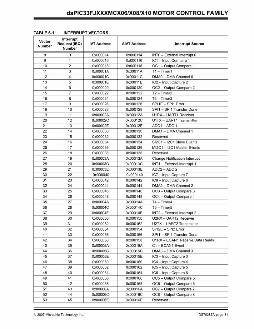
dsPIC33FJXXXMCX06/X08/X10 MOTOR CONTROL FAMILY
TABLE 6-1: INTERRUPT VECTORS
Vector Number
Interrupt Request (IRQ)
NumberIVT Address AIVT Address Interrupt Source
8 0 0x000014 0x000114 INT0 – External Interrupt 09 1 0x000016 0x000116 IC1 – Input Compare 1
10 2 0x000018 0x000118 OC1 – Output Compare 111 3 0x00001A 0x00011A T1 – Timer112 4 0x00001C 0x00011C DMA0 – DMA Channel 013 5 0x00001E 0x00011E IC2 – Input Capture 214 6 0x000020 0x000120 OC2 – Output Compare 215 7 0x000022 0x000122 T2 – Timer216 8 0x000024 0x000124 T3 – Timer317 9 0x000026 0x000126 SPI1E – SPI1 Error 18 10 0x000028 0x000128 SPI1 – SPI1 Transfer Done19 11 0x00002A 0x00012A U1RX – UART1 Receiver20 12 0x00002C 0x00012C U1TX – UART1 Transmitter21 13 0x00002E 0x00012E ADC1 – ADC 122 14 0x000030 0x000130 DMA1 – DMA Channel 123 15 0x000032 0x000132 Reserved24 16 0x000034 0x000134 SI2C1 – I2C1 Slave Events25 17 0x000036 0x000136 MI2C1 – I2C1 Master Events26 18 0x000038 0x000138 Reserved27 19 0x00003A 0x00013A Change Notification Interrupt28 20 0x00003C 0x00013C INT1 – External Interrupt 129 21 0x00003E 0x00013E ADC2 – ADC 230 22 0x000040 0x000140 IC7 – Input Capture 731 23 0x000042 0x000142 IC8 – Input Capture 832 24 0x000044 0x000144 DMA2 – DMA Channel 233 25 0x000046 0x000146 OC3 – Output Compare 334 26 0x000048 0x000148 OC4 – Output Compare 435 27 0x00004A 0x00014A T4 – Timer436 28 0x00004C 0x00014C T5 – Timer537 29 0x00004E 0x00014E INT2 – External Interrupt 238 30 0x000050 0x000150 U2RX – UART2 Receiver39 31 0x000052 0x000152 U2TX – UART2 Transmitter40 32 0x000054 0x000154 SPI2E – SPI2 Error41 33 0x000056 0x000156 SPI1 – SPI1 Transfer Done42 34 0x000058 0x000158 C1RX – ECAN1 Receive Data Ready 43 35 0x00005A 0x00015A C1 – ECAN1 Event44 36 0x00005C 0x00015C DMA3 – DMA Channel 345 37 0x00005E 0x00015E IC3 – Input Capture 346 38 0x000060 0x000160 IC4 – Input Capture 447 39 0x000062 0x000162 IC5 – Input Capture 548 40 0x000064 0x000164 IC6 – Input Capture 649 41 0x000066 0x000166 OC5 – Output Compare 550 42 0x000068 0x000168 OC6 – Output Compare 651 43 0x00006A 0x00016A OC7 – Output Compare 752 44 0x00006C 0x00016C OC8 – Output Compare 853 45 0x00006E 0x00016E Reserved
© 2007 Microchip Technology Inc. DS70287A-page 81
dsPIC33FJXXXMCX06/X08/X10 MOTOR CONTROL FAMILY
TABLE 6-2: TRAP VECTORS
54 46 0x000070 0x000170 DMA4 – DMA Channel 455 47 0x000072 0x000172 T6 – Timer656 48 0x000074 0x000174 T7 – Timer757 49 0x000076 0x000176 SI2C2 – I2C2 Slave Events58 50 0x000078 0x000178 MI2C2 – I2C2 Master Events59 51 0x00007A 0x00017A T8 – Timer860 52 0x00007C 0x00017C T9 – Timer961 53 0x00007E 0x00017E INT3 – External Interrupt 362 54 0x000080 0x000180 INT4 – External Interrupt 463 55 0x000082 0x000182 C2RX – ECAN2 Receive Data Ready 64 56 0x000084 0x000184 C2 – ECAN2 Event65 57 0x000086 0x000186 PWM – PWM Period Match66 58 0x000088 0x000188 QEI – Position Counter Compare69 61 0x00008E 0x00018E DMA5 – DMA Channel 570 62 0x000090 0x000190 Reserved71 63 0x000092 0x000192 FLTA – MCPWM Fault A72 64 0x000094 0x000194 FLTB – MCPWM Fault B73 65 0x000096 0x000196 U1E – UART1 Error74 66 0x000098 0x000198 U2E – UART2 Error75 67 0x00009A 0x00019A Reserved76 68 0x00009C 0x00019C DMA6 – DMA Channel 677 69 0x00009E 0x00019E DMA7 – DMA Channel 778 70 0x0000A0 0x0001A0 C1TX – ECAN1 Transmit Data Request79 71 0x0000A2 0x0001A2 C2TX – ECAN2 Transmit Data Request
80-125 72-117 0x0000A4-0x0000FE
0x0001A4-0x0001FE
Reserved
Vector Number IVT Address AIVT Address Trap Source
0 0x000004 0x000104 Reserved1 0x000006 0x000106 Oscillator Failure2 0x000008 0x000108 Address Error3 0x00000A 0x00010A Stack Error4 0x00000C 0x00010C Math Error5 0x00000E 0x00010E DMA Error Trap6 0x000010 0x000110 Reserved7 0x000012 0x000112 Reserved
TABLE 6-1: INTERRUPT VECTORS (CONTINUED)
Vector Number
Interrupt Request (IRQ)
NumberIVT Address AIVT Address Interrupt Source
DS70287A-page 82 © 2007 Microchip Technology Inc.
dsPIC33FJXXXMCX06/X08/X10 MOTOR CONTROL FAMILY
6.3 Interrupt Control and Status Registers
dsPIC33FJXXXMCX06/X08/X10 Motor Control Familydevices implement a total of 30 registers for the inter-rupt controller:
• INTCON1 • INTCON2 • IFS0 through IFS4• IEC0 through IEC4• IPC0 through IPC17 • INTTREG
Global interrupt control functions are controlled fromINTCON1 and INTCON2. INTCON1 contains theInterrupt Nesting Disable (NSTDIS) bit as well as thecontrol and status flags for the processor trap sources.The INTCON2 register controls the external interruptrequest signal behavior and the use of the AlternateInterrupt Vector Table.
The IFS registers maintain all of the interrupt requestflags. Each source of interrupt has a Status bit, which isset by the respective peripherals or external signal andis cleared via software.
The IEC registers maintain all of the interrupt enablebits. These control bits are used to individually enableinterrupts from the peripherals or external signals.
The IPC registers are used to set the interrupt prioritylevel for each source of interrupt. Each user interruptsource can be assigned to one of eight priority levels.
The INTTREG register contains the associatedinterrupt vector number and the new CPU interruptpriority level, which are latched into vector number(VECNUM<6:0>) and Interrupt level (ILR<3:0>) bitfields in the INTTREG register. The new interrupt prior-ity level is the priority of the pending interrupt.
The interrupt sources are assigned to the IFSx, IECxand IPCx registers in the same sequence that they arelisted in Table 6-1. For example, the INT0 (ExternalInterrupt 0) is shown as having vector number 8 and anatural order priority of 0. Thus, the INT0IF bit is foundin IFS0<0>, the INT0IE bit in IEC0<0> and the INT0IPbits in the first position of IPC0 (IPC0<2:0>).
Although they are not specifically part of the interruptcontrol hardware, two of the CPU Control registerscontain bits that control interrupt functionality. The CPUSTATUS register, SR, contains the IPL<2:0> bits(SR<7:5>). These bits indicate the current CPUinterrupt priority level. The user can change the currentCPU priority level by writing to the IPL bits.
The CORCON register contains the IPL3 bit which,together with IPL<2:0>, also indicates the current CPUpriority level. IPL3 is a read-only bit so that trap eventscannot be masked by the user software.
All Interrupt registers are described in Register 6-1through Register 6-32 in the following pages.
© 2007 Microchip Technology Inc. DS70287A-page 83
dsPIC33FJXXXMCX06/X08/X10 MOTOR CONTROL FAMILY
REGISTER 6-1: SR: CPU STATUS REGISTER(1)
R-0 R-0 R/C-0 R/C-0 R-0 R/C-0 R -0 R/W-0OA OB SA SB OAB SAB DA DC
bit 15 bit 8
R/W-0(3) R/W-0(3) R/W-0(3) R-0 R/W-0 R/W-0 R/W-0 R/W-0IPL2(2) IPL1(2) IPL0(2) RA N OV Z C
bit 7 bit 0
Legend:C = Clear only bit R = Readable bit U = Unimplemented bit, read as ‘0’S = Set only bit W = Writable bit -n = Value at POR‘1’ = Bit is set ‘0’ = Bit is cleared x = Bit is unknown
bit 7-5 IPL<2:0>: CPU Interrupt Priority Level Status bits(1)
111 = CPU Interrupt Priority Level is 7 (15), user interrupts disabled110 = CPU Interrupt Priority Level is 6 (14)101 = CPU Interrupt Priority Level is 5 (13)100 = CPU Interrupt Priority Level is 4 (12)011 = CPU Interrupt Priority Level is 3 (11)010 = CPU Interrupt Priority Level is 2 (10)001 = CPU Interrupt Priority Level is 1 (9)000 = CPU Interrupt Priority Level is 0 (8)
Note 1: For complete register details, see Register 2-1: “SR: CPU STATUS Register”.2: The IPL<2:0> bits are concatenated with the IPL<3> bit (CORCON<3>) to form the CPU Interrupt Priority
Level. The value in parentheses indicates the IPL if IPL<3> = 1. User interrupts are disabled when IPL<3> = 1.
3: The IPL<2:0> Status bits are read-only when NSTDIS (INTCON1<15>) = 1.
REGISTER 6-2: CORCON: CORE CONTROL REGISTER(1)
U-0 U-0 U-0 R/W-0 R/W-0 R-0 R-0 R-0— — — US EDT DL<2:0>
bit 15 bit 8
R/W-0 R/W-0 R/W-1 R/W-0 R/C-0 R/W-0 R/W-0 R/W-0SATA SATB SATDW ACCSAT IPL3(2) PSV RND IF
bit 7 bit 0
Legend: C = Clear only bitR = Readable bit W = Writable bit -n = Value at POR ‘1’ = Bit is set0’ = Bit is cleared ‘x = Bit is unknown U = Unimplemented bit, read as ‘0’
bit 3 IPL3: CPU Interrupt Priority Level Status bit 3(2)
1 = CPU interrupt priority level is greater than 70 = CPU interrupt priority level is 7 or less
Note 1: For complete register details, see Register 2-2: “CORCON: CORE Control Register”.2: The IPL3 bit is concatenated with the IPL<2:0> bits (SR<7:5>) to form the CPU Interrupt Priority Level.
DS70287A-page 84 © 2007 Microchip Technology Inc.
dsPIC33FJXXXMCX06/X08/X10 MOTOR CONTROL FAMILY
REGISTER 6-3: INTCON1: INTERRUPT CONTROL REGISTER 1
R/W-0 R/W-0 R/W-0 R/W-0 R/W-0 R/W-0 R/W-0 R/W-0NSTDIS OVAERR OVBERR COVAERR COVBERR OVATE OVBTE COVTE
bit 15 bit 8
R/W-0 R/W-0 R/W-0 R/W-0 R/W-0 R/W-0 R/W-0 U-0SFTACERR DIV0ERR DMACERR MATHERR ADDRERR STKERR OSCFAIL —
bit 7 bit 0
Legend:R = Readable bit W = Writable bit U = Unimplemented bit, read as ‘0’-n = Value at POR ‘1’ = Bit is set ‘0’ = Bit is cleared x = Bit is unknown
bit 15 NSTDIS: Interrupt Nesting Disable bit1 = Interrupt nesting is disabled0 = Interrupt nesting is enabled
bit 14 OVAERR: Accumulator A Overflow Trap Flag bit1 = Trap was caused by overflow of Accumulator A0 = Trap was not caused by overflow of Accumulator A
bit 13 OVBERR: Accumulator B Overflow Trap Flag bit1 = Trap was caused by overflow of Accumulator B0 = Trap was not caused by overflow of Accumulator B
bit 12 COVAERR: Accumulator A Catastrophic Overflow Trap Enable bit1 = Trap was caused by catastrophic overflow of Accumulator A 0 = Trap was not caused by catastrophic overflow of Accumulator A
bit 11 COVBERR: Accumulator B Catastrophic Overflow Trap Enable bit1 = Trap was caused by catastrophic overflow of Accumulator B 0 = Trap was not caused by catastrophic overflow of Accumulator B
bit 10 OVATE: Accumulator A Overflow Trap Enable bit1 = Trap overflow of Accumulator A0 = Trap disabled
bit 9 OVBTE: Accumulator B Overflow Trap Enable bit1 = Trap overflow of Accumulator B0 = Trap disabled
bit 8 COVTE: Catastrophic Overflow Trap Enable bit1 = Trap on catastrophic overflow of Accumulator A or B enabled0 = Trap disabled
bit 7 SFTACERR: Shift Accumulator Error Status bit1 = Math error trap was caused by an invalid accumulator shift0 = Math error trap was not caused by an invalid accumulator shift
bit 6 DIV0ERR: Arithmetic Error Status bit1 = Math error trap was caused by a divide by zero0 = Math error trap was not caused by a divide by zero
bit 5 DMACERR: DMA Controller Error Status bit1 = DMA controller error trap has occurred0 = DMA controller error trap has not occurred
bit 4 MATHERR: Arithmetic Error Status bit1 = Math error trap has occurred0 = Math error trap has not occurred
© 2007 Microchip Technology Inc. DS70287A-page 85
dsPIC33FJXXXMCX06/X08/X10 MOTOR CONTROL FAMILY
bit 3 ADDRERR: Address Error Trap Status bit1 = Address error trap has occurred0 = Address error trap has not occurred
bit 2 STKERR: Stack Error Trap Status bit1 = Stack error trap has occurred0 = Stack error trap has not occurred
bit 1 OSCFAIL: Oscillator Failure Trap Status bit1 = Oscillator failure trap has occurred0 = Oscillator failure trap has not occurred
bit 0 Unimplemented: Read as ‘0’
REGISTER 6-3: INTCON1: INTERRUPT CONTROL REGISTER 1 (CONTINUED)
DS70287A-page 86 © 2007 Microchip Technology Inc.
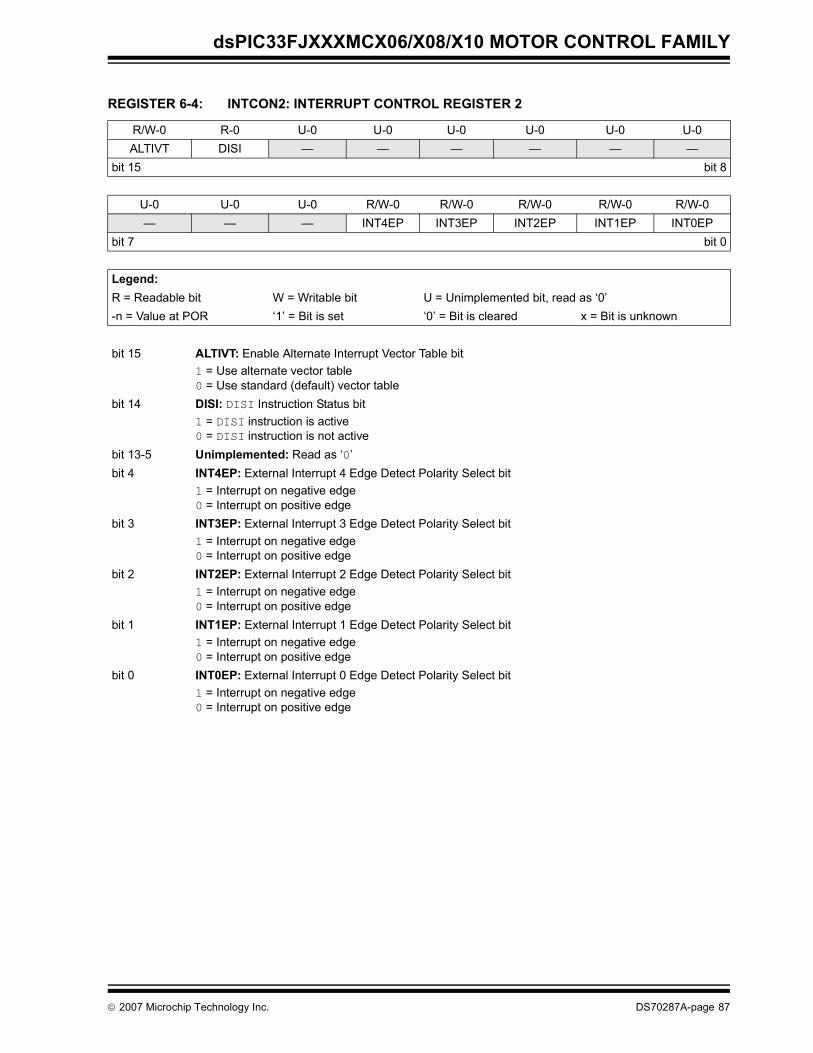
dsPIC33FJXXXMCX06/X08/X10 MOTOR CONTROL FAMILY
REGISTER 6-4: INTCON2: INTERRUPT CONTROL REGISTER 2
R/W-0 R-0 U-0 U-0 U-0 U-0 U-0 U-0ALTIVT DISI — — — — — —
bit 15 bit 8
U-0 U-0 U-0 R/W-0 R/W-0 R/W-0 R/W-0 R/W-0— — — INT4EP INT3EP INT2EP INT1EP INT0EP
bit 7 bit 0
Legend:R = Readable bit W = Writable bit U = Unimplemented bit, read as ‘0’-n = Value at POR ‘1’ = Bit is set ‘0’ = Bit is cleared x = Bit is unknown
bit 15 ALTIVT: Enable Alternate Interrupt Vector Table bit1 = Use alternate vector table0 = Use standard (default) vector table
bit 14 DISI: DISI Instruction Status bit1 = DISI instruction is active0 = DISI instruction is not active
bit 13-5 Unimplemented: Read as ‘0’bit 4 INT4EP: External Interrupt 4 Edge Detect Polarity Select bit
1 = Interrupt on negative edge 0 = Interrupt on positive edge
bit 3 INT3EP: External Interrupt 3 Edge Detect Polarity Select bit1 = Interrupt on negative edge 0 = Interrupt on positive edge
bit 2 INT2EP: External Interrupt 2 Edge Detect Polarity Select bit1 = Interrupt on negative edge 0 = Interrupt on positive edge
bit 1 INT1EP: External Interrupt 1 Edge Detect Polarity Select bit1 = Interrupt on negative edge 0 = Interrupt on positive edge
bit 0 INT0EP: External Interrupt 0 Edge Detect Polarity Select bit1 = Interrupt on negative edge 0 = Interrupt on positive edge
© 2007 Microchip Technology Inc. DS70287A-page 87
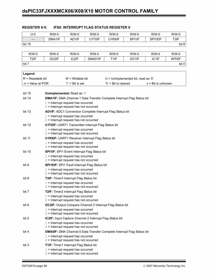
dsPIC33FJXXXMCX06/X08/X10 MOTOR CONTROL FAMILY
REGISTER 6-5: IFS0: INTERRUPT FLAG STATUS REGISTER 0
U-0 R/W-0 R/W-0 R/W-0 R/W-0 R/W-0 R/W-0 R/W-0— DMA1IF AD1IF U1TXIF U1RXIF SPI1IF SPI1EIF T3IF
bit 15 bit 8
R/W-0 R/W-0 R/W-0 R/W-0 R/W-0 R/W-0 R/W-0 R/W-0T2IF OC2IF IC2IF DMA01IF T1IF OC1IF IC1IF INT0IF
bit 7 bit 0
Legend:R = Readable bit W = Writable bit U = Unimplemented bit, read as ‘0’-n = Value at POR ‘1’ = Bit is set ‘0’ = Bit is cleared x = Bit is unknown
bit 15 Unimplemented: Read as ‘0’bit 14 DMA1IF: DMA Channel 1 Data Transfer Complete Interrupt Flag Status bit
1 = Interrupt request has occurred0 = Interrupt request has not occurred
bit 13 AD1IF: ADC1 Conversion Complete Interrupt Flag Status bit1 = Interrupt request has occurred0 = Interrupt request has not occurred
bit 12 U1TXIF: UART1 Transmitter Interrupt Flag Status bit1 = Interrupt request has occurred0 = Interrupt request has not occurred
bit 11 U1RXIF: UART1 Receiver Interrupt Flag Status bit1 = Interrupt request has occurred0 = Interrupt request has not occurred
bit 10 SPI1IF: SPI1 Event Interrupt Flag Status bit1 = Interrupt request has occurred0 = Interrupt request has not occurred
bit 9 SPI1EIF: SPI1 Fault Interrupt Flag Status bit1 = Interrupt request has occurred0 = Interrupt request has not occurred
bit 8 T3IF: Timer3 Interrupt Flag Status bit1 = Interrupt request has occurred0 = Interrupt request has not occurred
bit 7 T2IF: Timer2 Interrupt Flag Status bit1 = Interrupt request has occurred0 = Interrupt request has not occurred
bit 6 OC2IF: Output Compare Channel 2 Interrupt Flag Status bit1 = Interrupt request has occurred0 = Interrupt request has not occurred
bit 5 IC2IF: Input Capture Channel 2 Interrupt Flag Status bit1 = Interrupt request has occurred0 = Interrupt request has not occurred
bit 4 DMA0IF: DMA Channel 0 Data Transfer Complete Interrupt Flag Status bit1 = Interrupt request has occurred0 = Interrupt request has not occurred
bit 3 T1IF: Timer1 Interrupt Flag Status bit1 = Interrupt request has occurred0 = Interrupt request has not occurred
DS70287A-page 88 © 2007 Microchip Technology Inc.
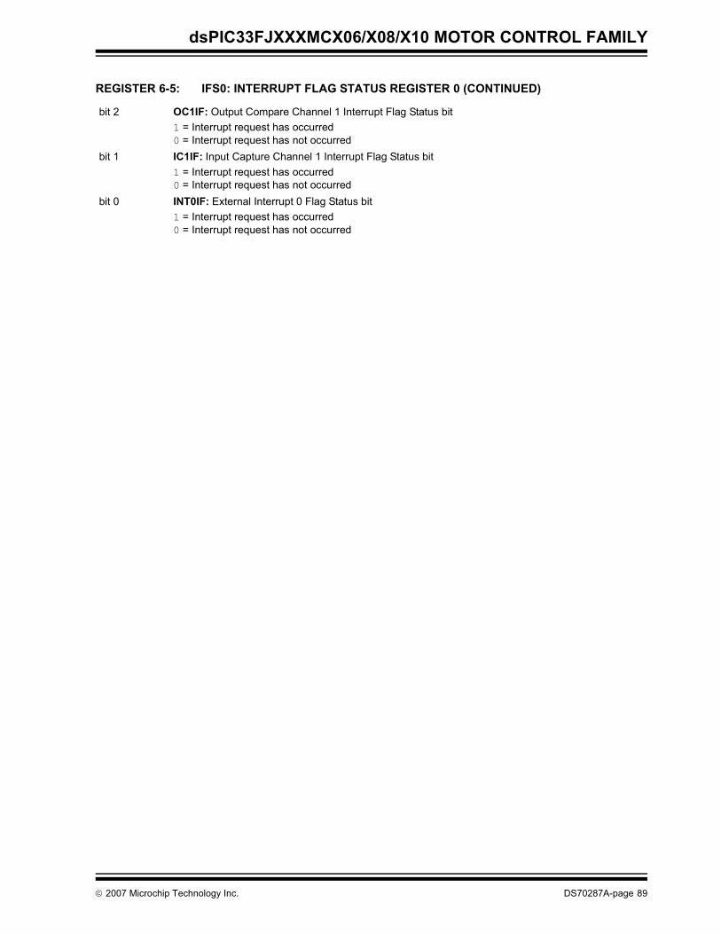
dsPIC33FJXXXMCX06/X08/X10 MOTOR CONTROL FAMILY
bit 2 OC1IF: Output Compare Channel 1 Interrupt Flag Status bit1 = Interrupt request has occurred0 = Interrupt request has not occurred
bit 1 IC1IF: Input Capture Channel 1 Interrupt Flag Status bit1 = Interrupt request has occurred0 = Interrupt request has not occurred
bit 0 INT0IF: External Interrupt 0 Flag Status bit1 = Interrupt request has occurred0 = Interrupt request has not occurred
REGISTER 6-5: IFS0: INTERRUPT FLAG STATUS REGISTER 0 (CONTINUED)
© 2007 Microchip Technology Inc. DS70287A-page 89
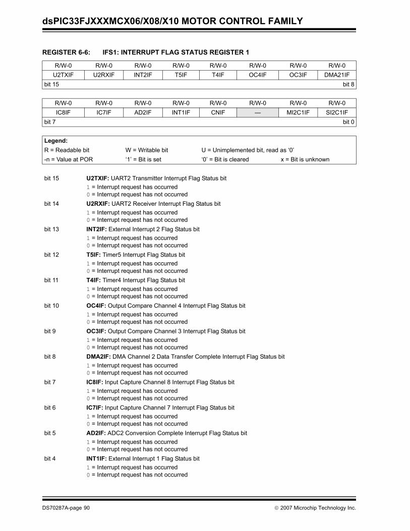
dsPIC33FJXXXMCX06/X08/X10 MOTOR CONTROL FAMILY
REGISTER 6-6: IFS1: INTERRUPT FLAG STATUS REGISTER 1
R/W-0 R/W-0 R/W-0 R/W-0 R/W-0 R/W-0 R/W-0 R/W-0U2TXIF U2RXIF INT2IF T5IF T4IF OC4IF OC3IF DMA21IF
bit 15 bit 8
R/W-0 R/W-0 R/W-0 R/W-0 R/W-0 R/W-0 R/W-0 R/W-0IC8IF IC7IF AD2IF INT1IF CNIF — MI2C1IF SI2C1IF
bit 7 bit 0
Legend:R = Readable bit W = Writable bit U = Unimplemented bit, read as ‘0’-n = Value at POR ‘1’ = Bit is set ‘0’ = Bit is cleared x = Bit is unknown
bit 15 U2TXIF: UART2 Transmitter Interrupt Flag Status bit1 = Interrupt request has occurred0 = Interrupt request has not occurred
bit 14 U2RXIF: UART2 Receiver Interrupt Flag Status bit1 = Interrupt request has occurred0 = Interrupt request has not occurred
bit 13 INT2IF: External Interrupt 2 Flag Status bit1 = Interrupt request has occurred0 = Interrupt request has not occurred
bit 12 T5IF: Timer5 Interrupt Flag Status bit1 = Interrupt request has occurred0 = Interrupt request has not occurred
bit 11 T4IF: Timer4 Interrupt Flag Status bit1 = Interrupt request has occurred0 = Interrupt request has not occurred
bit 10 OC4IF: Output Compare Channel 4 Interrupt Flag Status bit1 = Interrupt request has occurred0 = Interrupt request has not occurred
bit 9 OC3IF: Output Compare Channel 3 Interrupt Flag Status bit1 = Interrupt request has occurred0 = Interrupt request has not occurred
bit 8 DMA2IF: DMA Channel 2 Data Transfer Complete Interrupt Flag Status bit1 = Interrupt request has occurred0 = Interrupt request has not occurred
bit 7 IC8IF: Input Capture Channel 8 Interrupt Flag Status bit1 = Interrupt request has occurred0 = Interrupt request has not occurred
bit 6 IC7IF: Input Capture Channel 7 Interrupt Flag Status bit1 = Interrupt request has occurred0 = Interrupt request has not occurred
bit 5 AD2IF: ADC2 Conversion Complete Interrupt Flag Status bit1 = Interrupt request has occurred0 = Interrupt request has not occurred
bit 4 INT1IF: External Interrupt 1 Flag Status bit1 = Interrupt request has occurred0 = Interrupt request has not occurred
DS70287A-page 90 © 2007 Microchip Technology Inc.
dsPIC33FJXXXMCX06/X08/X10 MOTOR CONTROL FAMILY
bit 3 CNIF: Input Change Notification Interrupt Flag Status bit1 = Interrupt request has occurred0 = Interrupt request has not occurred
bit 2 Unimplemented: Read as ‘0’bit 1 MI2C1IF: I2C1 Master Events Interrupt Flag Status bit
1 = Interrupt request has occurred0 = Interrupt request has not occurred
bit 0 SI2C1IF: I2C1 Slave Events Interrupt Flag Status bit1 = Interrupt request has occurred0 = Interrupt request has not occurred
REGISTER 6-6: IFS1: INTERRUPT FLAG STATUS REGISTER 1 (CONTINUED)
© 2007 Microchip Technology Inc. DS70287A-page 91
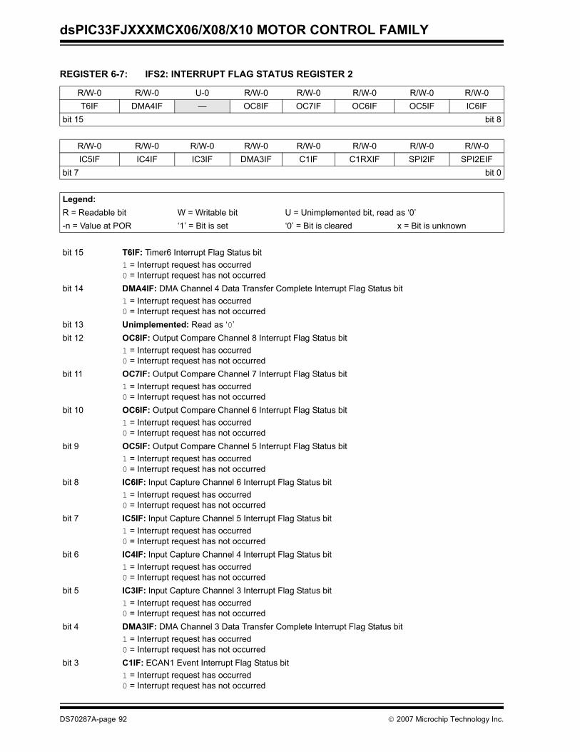
dsPIC33FJXXXMCX06/X08/X10 MOTOR CONTROL FAMILY
REGISTER 6-7: IFS2: INTERRUPT FLAG STATUS REGISTER 2
R/W-0 R/W-0 U-0 R/W-0 R/W-0 R/W-0 R/W-0 R/W-0T6IF DMA4IF — OC8IF OC7IF OC6IF OC5IF IC6IF
bit 15 bit 8
R/W-0 R/W-0 R/W-0 R/W-0 R/W-0 R/W-0 R/W-0 R/W-0IC5IF IC4IF IC3IF DMA3IF C1IF C1RXIF SPI2IF SPI2EIF
bit 7 bit 0
Legend:R = Readable bit W = Writable bit U = Unimplemented bit, read as ‘0’-n = Value at POR ‘1’ = Bit is set ‘0’ = Bit is cleared x = Bit is unknown
bit 15 T6IF: Timer6 Interrupt Flag Status bit1 = Interrupt request has occurred0 = Interrupt request has not occurred
bit 14 DMA4IF: DMA Channel 4 Data Transfer Complete Interrupt Flag Status bit1 = Interrupt request has occurred0 = Interrupt request has not occurred
bit 13 Unimplemented: Read as ‘0’bit 12 OC8IF: Output Compare Channel 8 Interrupt Flag Status bit
1 = Interrupt request has occurred0 = Interrupt request has not occurred
bit 11 OC7IF: Output Compare Channel 7 Interrupt Flag Status bit1 = Interrupt request has occurred0 = Interrupt request has not occurred
bit 10 OC6IF: Output Compare Channel 6 Interrupt Flag Status bit1 = Interrupt request has occurred0 = Interrupt request has not occurred
bit 9 OC5IF: Output Compare Channel 5 Interrupt Flag Status bit1 = Interrupt request has occurred0 = Interrupt request has not occurred
bit 8 IC6IF: Input Capture Channel 6 Interrupt Flag Status bit1 = Interrupt request has occurred0 = Interrupt request has not occurred
bit 7 IC5IF: Input Capture Channel 5 Interrupt Flag Status bit1 = Interrupt request has occurred0 = Interrupt request has not occurred
bit 6 IC4IF: Input Capture Channel 4 Interrupt Flag Status bit1 = Interrupt request has occurred0 = Interrupt request has not occurred
bit 5 IC3IF: Input Capture Channel 3 Interrupt Flag Status bit1 = Interrupt request has occurred0 = Interrupt request has not occurred
bit 4 DMA3IF: DMA Channel 3 Data Transfer Complete Interrupt Flag Status bit1 = Interrupt request has occurred0 = Interrupt request has not occurred
bit 3 C1IF: ECAN1 Event Interrupt Flag Status bit1 = Interrupt request has occurred0 = Interrupt request has not occurred
DS70287A-page 92 © 2007 Microchip Technology Inc.

dsPIC33FJXXXMCX06/X08/X10 MOTOR CONTROL FAMILY
bit 2 C1RXIF: ECAN1 Receive Data Ready Interrupt Flag Status bit1 = Interrupt request has occurred0 = Interrupt request has not occurred
bit 1 SPI2IF: SPI2 Event Interrupt Flag Status bit1 = Interrupt request has occurred0 = Interrupt request has not occurred
bit 0 SPI2EIF: SPI2 Error Interrupt Flag Status bit1 = Interrupt request has occurred0 = Interrupt request has not occurred
REGISTER 6-7: IFS2: INTERRUPT FLAG STATUS REGISTER 2 (CONTINUED)
© 2007 Microchip Technology Inc. DS70287A-page 93
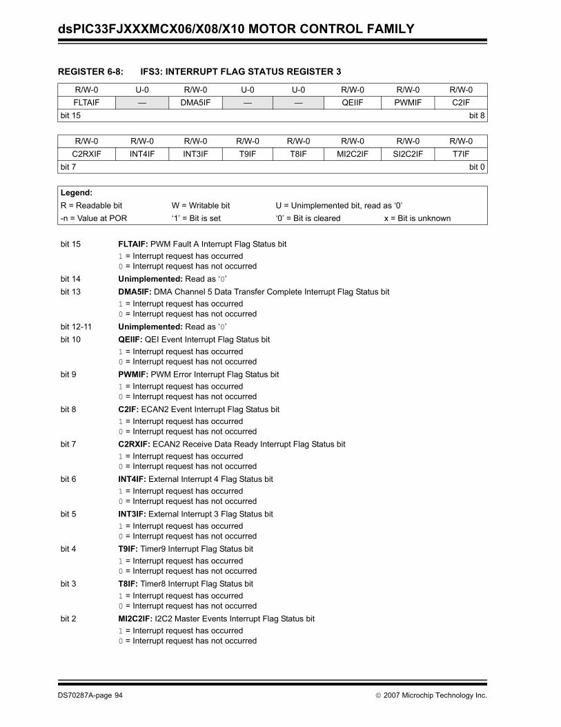
dsPIC33FJXXXMCX06/X08/X10 MOTOR CONTROL FAMILY
REGISTER 6-8: IFS3: INTERRUPT FLAG STATUS REGISTER 3
R/W-0 U-0 R/W-0 U-0 U-0 R/W-0 R/W-0 R/W-0FLTAIF — DMA5IF — — QEIIF PWMIF C2IF
bit 15 bit 8
R/W-0 R/W-0 R/W-0 R/W-0 R/W-0 R/W-0 R/W-0 R/W-0C2RXIF INT4IF INT3IF T9IF T8IF MI2C2IF SI2C2IF T7IF
bit 7 bit 0
Legend:R = Readable bit W = Writable bit U = Unimplemented bit, read as ‘0’-n = Value at POR ‘1’ = Bit is set ‘0’ = Bit is cleared x = Bit is unknown
bit 15 FLTAIF: PWM Fault A Interrupt Flag Status bit1 = Interrupt request has occurred0 = Interrupt request has not occurred
bit 14 Unimplemented: Read as ‘0’bit 13 DMA5IF: DMA Channel 5 Data Transfer Complete Interrupt Flag Status bit
1 = Interrupt request has occurred0 = Interrupt request has not occurred
bit 12-11 Unimplemented: Read as ‘0’bit 10 QEIIF: QEI Event Interrupt Flag Status bit
1 = Interrupt request has occurred0 = Interrupt request has not occurred
bit 9 PWMIF: PWM Error Interrupt Flag Status bit1 = Interrupt request has occurred0 = Interrupt request has not occurred
bit 8 C2IF: ECAN2 Event Interrupt Flag Status bit1 = Interrupt request has occurred0 = Interrupt request has not occurred
bit 7 C2RXIF: ECAN2 Receive Data Ready Interrupt Flag Status bit1 = Interrupt request has occurred0 = Interrupt request has not occurred
bit 6 INT4IF: External Interrupt 4 Flag Status bit1 = Interrupt request has occurred0 = Interrupt request has not occurred
bit 5 INT3IF: External Interrupt 3 Flag Status bit1 = Interrupt request has occurred0 = Interrupt request has not occurred
bit 4 T9IF: Timer9 Interrupt Flag Status bit1 = Interrupt request has occurred0 = Interrupt request has not occurred
bit 3 T8IF: Timer8 Interrupt Flag Status bit1 = Interrupt request has occurred0 = Interrupt request has not occurred
bit 2 MI2C2IF: I2C2 Master Events Interrupt Flag Status bit1 = Interrupt request has occurred0 = Interrupt request has not occurred
DS70287A-page 94 © 2007 Microchip Technology Inc.
dsPIC33FJXXXMCX06/X08/X10 MOTOR CONTROL FAMILY
bit 1 SI2C2IF: I2C2 Slave Events Interrupt Flag Status bit1 = Interrupt request has occurred0 = Interrupt request has not occurred
bit 0 T7IF: Timer7 Interrupt Flag Status bit1 = Interrupt request has occurred0 = Interrupt request has not occurred
REGISTER 6-8: IFS3: INTERRUPT FLAG STATUS REGISTER 3 (CONTINUED)
© 2007 Microchip Technology Inc. DS70287A-page 95
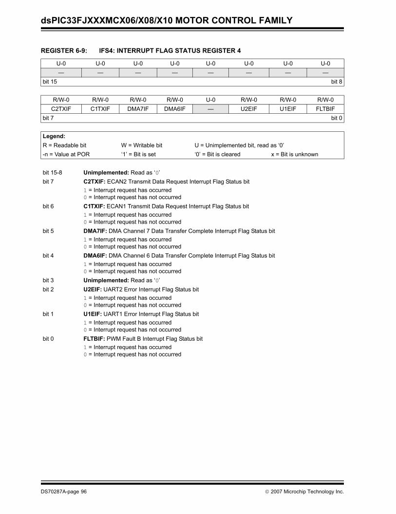
dsPIC33FJXXXMCX06/X08/X10 MOTOR CONTROL FAMILY
REGISTER 6-9: IFS4: INTERRUPT FLAG STATUS REGISTER 4
U-0 U-0 U-0 U-0 U-0 U-0 U-0 U-0— — — — — — — —
bit 15 bit 8
R/W-0 R/W-0 R/W-0 R/W-0 U-0 R/W-0 R/W-0 R/W-0C2TXIF C1TXIF DMA7IF DMA6IF — U2EIF U1EIF FLTBIF
bit 7 bit 0
Legend:R = Readable bit W = Writable bit U = Unimplemented bit, read as ‘0’-n = Value at POR ‘1’ = Bit is set ‘0’ = Bit is cleared x = Bit is unknown
bit 15-8 Unimplemented: Read as ‘0’bit 7 C2TXIF: ECAN2 Transmit Data Request Interrupt Flag Status bit
1 = Interrupt request has occurred0 = Interrupt request has not occurred
bit 6 C1TXIF: ECAN1 Transmit Data Request Interrupt Flag Status bit1 = Interrupt request has occurred0 = Interrupt request has not occurred
bit 5 DMA7IF: DMA Channel 7 Data Transfer Complete Interrupt Flag Status bit1 = Interrupt request has occurred0 = Interrupt request has not occurred
bit 4 DMA6IF: DMA Channel 6 Data Transfer Complete Interrupt Flag Status bit1 = Interrupt request has occurred0 = Interrupt request has not occurred
bit 3 Unimplemented: Read as ‘0’bit 2 U2EIF: UART2 Error Interrupt Flag Status bit
1 = Interrupt request has occurred0 = Interrupt request has not occurred
bit 1 U1EIF: UART1 Error Interrupt Flag Status bit1 = Interrupt request has occurred0 = Interrupt request has not occurred
bit 0 FLTBIF: PWM Fault B Interrupt Flag Status bit1 = Interrupt request has occurred0 = Interrupt request has not occurred
DS70287A-page 96 © 2007 Microchip Technology Inc.
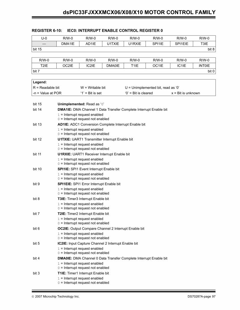
dsPIC33FJXXXMCX06/X08/X10 MOTOR CONTROL FAMILY
REGISTER 6-10: IEC0: INTERRUPT ENABLE CONTROL REGISTER 0
U-0 R/W-0 R/W-0 R/W-0 R/W-0 R/W-0 R/W-0 R/W-0— DMA1IE AD1IE U1TXIE U1RXIE SPI1IE SPI1EIE T3IE
bit 15 bit 8
R/W-0 R/W-0 R/W-0 R/W-0 R/W-0 R/W-0 R/W-0 R/W-0T2IE OC2IE IC2IE DMA0IE T1IE OC1IE IC1IE INT0IE
bit 7 bit 0
Legend:R = Readable bit W = Writable bit U = Unimplemented bit, read as ‘0’-n = Value at POR ‘1’ = Bit is set ‘0’ = Bit is cleared x = Bit is unknown
bit 15 Unimplemented: Read as ‘0’bit 14 DMA1IE: DMA Channel 1 Data Transfer Complete Interrupt Enable bit
1 = Interrupt request enabled0 = Interrupt request not enabled
bit 13 AD1IE: ADC1 Conversion Complete Interrupt Enable bit1 = Interrupt request enabled0 = Interrupt request not enabled
bit 12 U1TXIE: UART1 Transmitter Interrupt Enable bit1 = Interrupt request enabled0 = Interrupt request not enabled
bit 11 U1RXIE: UART1 Receiver Interrupt Enable bit1 = Interrupt request enabled0 = Interrupt request not enabled
bit 10 SPI1IE: SPI1 Event Interrupt Enable bit1 = Interrupt request enabled0 = Interrupt request not enabled
bit 9 SPI1EIE: SPI1 Error Interrupt Enable bit1 = Interrupt request enabled0 = Interrupt request not enabled
bit 8 T3IE: Timer3 Interrupt Enable bit1 = Interrupt request enabled0 = Interrupt request not enabled
bit 7 T2IE: Timer2 Interrupt Enable bit1 = Interrupt request enabled0 = Interrupt request not enabled
bit 6 OC2IE: Output Compare Channel 2 Interrupt Enable bit1 = Interrupt request enabled0 = Interrupt request not enabled
bit 5 IC2IE: Input Capture Channel 2 Interrupt Enable bit1 = Interrupt request enabled0 = Interrupt request not enabled
bit 4 DMA0IE: DMA Channel 0 Data Transfer Complete Interrupt Enable bit1 = Interrupt request enabled0 = Interrupt request not enabled
bit 3 T1IE: Timer1 Interrupt Enable bit1 = Interrupt request enabled0 = Interrupt request not enabled
© 2007 Microchip Technology Inc. DS70287A-page 97

dsPIC33FJXXXMCX06/X08/X10 MOTOR CONTROL FAMILY
bit 2 OC1IE: Output Compare Channel 1 Interrupt Enable bit1 = Interrupt request enabled0 = Interrupt request not enabled
bit 1 IC1IE: Input Capture Channel 1 Interrupt Enable bit1 = Interrupt request enabled0 = Interrupt request not enabled
bit 0 INT0IE: External Interrupt 0 Enable bit1 = Interrupt request enabled0 = Interrupt request not enabled
REGISTER 6-10: IEC0: INTERRUPT ENABLE CONTROL REGISTER 0 (CONTINUED)
DS70287A-page 98 © 2007 Microchip Technology Inc.
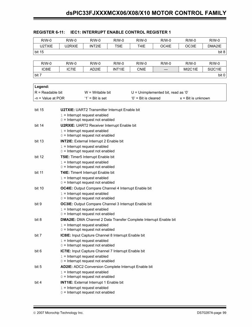
dsPIC33FJXXXMCX06/X08/X10 MOTOR CONTROL FAMILY
REGISTER 6-11: IEC1: INTERRUPT ENABLE CONTROL REGISTER 1
R/W-0 R/W-0 R/W-0 R/W-0 R/W-0 R/W-0 R/W-0 R/W-0U2TXIE U2RXIE INT2IE T5IE T4IE OC4IE OC3IE DMA2IE
bit 15 bit 8
R/W-0 R/W-0 R/W-0 R/W-0 R/W-0 R/W-0 R/W-0 R/W-0IC8IE IC7IE AD2IE INT1IE CNIE — MI2C1IE SI2C1IE
bit 7 bit 0
Legend:R = Readable bit W = Writable bit U = Unimplemented bit, read as ‘0’-n = Value at POR ‘1’ = Bit is set ‘0’ = Bit is cleared x = Bit is unknown
bit 15 U2TXIE: UART2 Transmitter Interrupt Enable bit1 = Interrupt request enabled0 = Interrupt request not enabled
bit 14 U2RXIE: UART2 Receiver Interrupt Enable bit1 = Interrupt request enabled0 = Interrupt request not enabled
bit 13 INT2IE: External Interrupt 2 Enable bit1 = Interrupt request enabled0 = Interrupt request not enabled
bit 12 T5IE: Timer5 Interrupt Enable bit1 = Interrupt request enabled0 = Interrupt request not enabled
bit 11 T4IE: Timer4 Interrupt Enable bit1 = Interrupt request enabled0 = Interrupt request not enabled
bit 10 OC4IE: Output Compare Channel 4 Interrupt Enable bit1 = Interrupt request enabled0 = Interrupt request not enabled
bit 9 OC3IE: Output Compare Channel 3 Interrupt Enable bit1 = Interrupt request enabled0 = Interrupt request not enabled
bit 8 DMA2IE: DMA Channel 2 Data Transfer Complete Interrupt Enable bit1 = Interrupt request enabled0 = Interrupt request not enabled
bit 7 IC8IE: Input Capture Channel 8 Interrupt Enable bit1 = Interrupt request enabled0 = Interrupt request not enabled
bit 6 IC7IE: Input Capture Channel 7 Interrupt Enable bit1 = Interrupt request enabled0 = Interrupt request not enabled
bit 5 AD2IE: ADC2 Conversion Complete Interrupt Enable bit1 = Interrupt request enabled0 = Interrupt request not enabled
bit 4 INT1IE: External Interrupt 1 Enable bit1 = Interrupt request enabled0 = Interrupt request not enabled
© 2007 Microchip Technology Inc. DS70287A-page 99
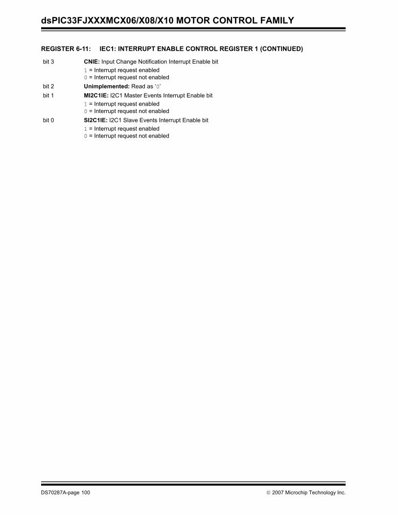
dsPIC33FJXXXMCX06/X08/X10 MOTOR CONTROL FAMILY
bit 3 CNIE: Input Change Notification Interrupt Enable bit1 = Interrupt request enabled0 = Interrupt request not enabled
bit 2 Unimplemented: Read as ‘0’bit 1 MI2C1IE: I2C1 Master Events Interrupt Enable bit
1 = Interrupt request enabled0 = Interrupt request not enabled
bit 0 SI2C1IE: I2C1 Slave Events Interrupt Enable bit1 = Interrupt request enabled0 = Interrupt request not enabled
REGISTER 6-11: IEC1: INTERRUPT ENABLE CONTROL REGISTER 1 (CONTINUED)
DS70287A-page 100 © 2007 Microchip Technology Inc.
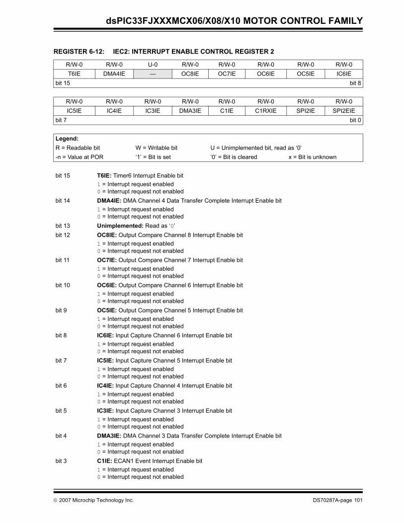
dsPIC33FJXXXMCX06/X08/X10 MOTOR CONTROL FAMILY
REGISTER 6-12: IEC2: INTERRUPT ENABLE CONTROL REGISTER 2
R/W-0 R/W-0 U-0 R/W-0 R/W-0 R/W-0 R/W-0 R/W-0T6IE DMA4IE — OC8IE OC7IE OC6IE OC5IE IC6IE
bit 15 bit 8
R/W-0 R/W-0 R/W-0 R/W-0 R/W-0 R/W-0 R/W-0 R/W-0IC5IE IC4IE IC3IE DMA3IE C1IE C1RXIE SPI2IE SPI2EIE
bit 7 bit 0
Legend:R = Readable bit W = Writable bit U = Unimplemented bit, read as ‘0’-n = Value at POR ‘1’ = Bit is set ‘0’ = Bit is cleared x = Bit is unknown
bit 15 T6IE: Timer6 Interrupt Enable bit1 = Interrupt request enabled0 = Interrupt request not enabled
bit 14 DMA4IE: DMA Channel 4 Data Transfer Complete Interrupt Enable bit1 = Interrupt request enabled0 = Interrupt request not enabled
bit 13 Unimplemented: Read as ‘0’ bit 12 OC8IE: Output Compare Channel 8 Interrupt Enable bit
1 = Interrupt request enabled0 = Interrupt request not enabled
bit 11 OC7IE: Output Compare Channel 7 Interrupt Enable bit1 = Interrupt request enabled0 = Interrupt request not enabled
bit 10 OC6IE: Output Compare Channel 6 Interrupt Enable bit1 = Interrupt request enabled0 = Interrupt request not enabled
bit 9 OC5IE: Output Compare Channel 5 Interrupt Enable bit1 = Interrupt request enabled0 = Interrupt request not enabled
bit 8 IC6IE: Input Capture Channel 6 Interrupt Enable bit1 = Interrupt request enabled0 = Interrupt request not enabled
bit 7 IC5IE: Input Capture Channel 5 Interrupt Enable bit1 = Interrupt request enabled0 = Interrupt request not enabled
bit 6 IC4IE: Input Capture Channel 4 Interrupt Enable bit1 = Interrupt request enabled0 = Interrupt request not enabled
bit 5 IC3IE: Input Capture Channel 3 Interrupt Enable bit1 = Interrupt request enabled0 = Interrupt request not enabled
bit 4 DMA3IE: DMA Channel 3 Data Transfer Complete Interrupt Enable bit1 = Interrupt request enabled0 = Interrupt request not enabled
bit 3 C1IE: ECAN1 Event Interrupt Enable bit1 = Interrupt request enabled0 = Interrupt request not enabled
© 2007 Microchip Technology Inc. DS70287A-page 101

dsPIC33FJXXXMCX06/X08/X10 MOTOR CONTROL FAMILY
bit 2 C1RXIE: ECAN1 Receive Data Ready Interrupt Enable bit1 = Interrupt request enabled0 = Interrupt request not enabled
bit 1 SPI2IE: SPI2 Event Interrupt Enable bit1 = Interrupt request enabled0 = Interrupt request not enabled
bit 0 SPI2EIE: SPI2 Error Interrupt Enable bit1 = Interrupt request enabled0 = Interrupt request not enabled
REGISTER 6-12: IEC2: INTERRUPT ENABLE CONTROL REGISTER 2 (CONTINUED)
DS70287A-page 102 © 2007 Microchip Technology Inc.
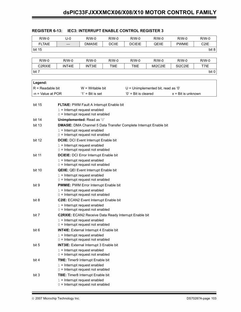
dsPIC33FJXXXMCX06/X08/X10 MOTOR CONTROL FAMILY
REGISTER 6-13: IEC3: INTERRUPT ENABLE CONTROL REGISTER 3
R/W-0 U-0 R/W-0 R/W-0 R/W-0 R/W-0 R/W-0 R/W-0FLTAIE — DMA5IE DCIIE DCIEIE QEIIE PWMIE C2IE
bit 15 bit 8
R/W-0 R/W-0 R/W-0 R/W-0 R/W-0 R/W-0 R/W-0 R/W-0C2RXIE INT4IE INT3IE T9IE T8IE MI2C2IE SI2C2IE T7IE
bit 7 bit 0
Legend:R = Readable bit W = Writable bit U = Unimplemented bit, read as ‘0’-n = Value at POR ‘1’ = Bit is set ‘0’ = Bit is cleared x = Bit is unknown
bit 15 FLTAIE: PWM Fault A Interrupt Enable bit1 = Interrupt request enabled0 = Interrupt request not enabled
bit 14 Unimplemented: Read as ‘0’bit 13 DMA5IE: DMA Channel 5 Data Transfer Complete Interrupt Enable bit
1 = Interrupt request enabled0 = Interrupt request not enabled
bit 12 DCIIE: DCI Event Interrupt Enable bit1 = Interrupt request enabled0 = Interrupt request not enabled
bit 11 DCIEIE: DCI Error Interrupt Enable bit1 = Interrupt request enabled0 = Interrupt request not enabled
bit 10 QEIIE: QEI Event Interrupt Enable bit1 = Interrupt request enabled0 = Interrupt request not enabled
bit 9 PWMIE: PWM Error Interrupt Enable bit1 = Interrupt request enabled0 = Interrupt request not enabled
bit 8 C2IE: ECAN2 Event Interrupt Enable bit1 = Interrupt request enabled0 = Interrupt request not enabled
bit 7 C2RXIE: ECAN2 Receive Data Ready Interrupt Enable bit1 = Interrupt request enabled0 = Interrupt request not enabled
bit 6 INT4IE: External Interrupt 4 Enable bit1 = Interrupt request enabled0 = Interrupt request not enabled
bit 5 INT3IE: External Interrupt 3 Enable bit1 = Interrupt request enabled0 = Interrupt request not enabled
bit 4 T9IE: Timer9 Interrupt Enable bit1 = Interrupt request enabled0 = Interrupt request not enabled
bit 3 T8IE: Timer8 Interrupt Enable bit1 = Interrupt request enabled0 = Interrupt request not enabled
© 2007 Microchip Technology Inc. DS70287A-page 103
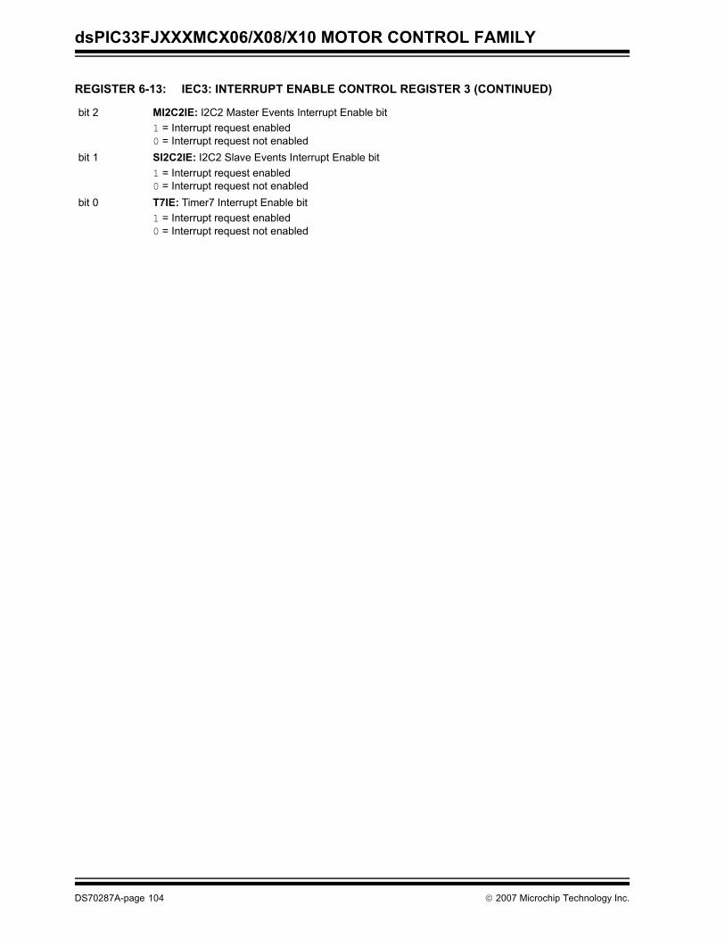
dsPIC33FJXXXMCX06/X08/X10 MOTOR CONTROL FAMILY
bit 2 MI2C2IE: I2C2 Master Events Interrupt Enable bit1 = Interrupt request enabled0 = Interrupt request not enabled
bit 1 SI2C2IE: I2C2 Slave Events Interrupt Enable bit1 = Interrupt request enabled0 = Interrupt request not enabled
bit 0 T7IE: Timer7 Interrupt Enable bit1 = Interrupt request enabled0 = Interrupt request not enabled
REGISTER 6-13: IEC3: INTERRUPT ENABLE CONTROL REGISTER 3 (CONTINUED)
DS70287A-page 104 © 2007 Microchip Technology Inc.
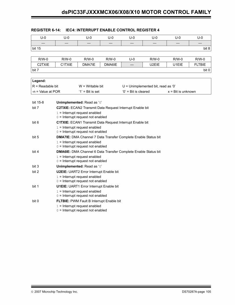
dsPIC33FJXXXMCX06/X08/X10 MOTOR CONTROL FAMILY
REGISTER 6-14: IEC4: INTERRUPT ENABLE CONTROL REGISTER 4
U-0 U-0 U-0 U-0 U-0 U-0 U-0 U-0— — — — — — — —
bit 15 bit 8
R/W-0 R/W-0 R/W-0 R/W-0 U-0 R/W-0 R/W-0 R/W-0C2TXIE C1TXIE DMA7IE DMA6IE — U2EIE U1EIE FLTBIE
bit 7 bit 0
Legend:R = Readable bit W = Writable bit U = Unimplemented bit, read as ‘0’-n = Value at POR ‘1’ = Bit is set ‘0’ = Bit is cleared x = Bit is unknown
bit 15-8 Unimplemented: Read as ‘0’bit 7 C2TXIE: ECAN2 Transmit Data Request Interrupt Enable bit
1 = Interrupt request enabled0 = Interrupt request not enabled
bit 6 C1TXIE: ECAN1 Transmit Data Request Interrupt Enable bit1 = Interrupt request enabled0 = Interrupt request not enabled
bit 5 DMA7IE: DMA Channel 7 Data Transfer Complete Enable Status bit1 = Interrupt request enabled0 = Interrupt request not enabled
bit 4 DMA6IE: DMA Channel 6 Data Transfer Complete Enable Status bit1 = Interrupt request enabled0 = Interrupt request not enabled
bit 3 Unimplemented: Read as ‘0’bit 2 U2EIE: UART2 Error Interrupt Enable bit
1 = Interrupt request enabled0 = Interrupt request not enabled
bit 1 U1EIE: UART1 Error Interrupt Enable bit1 = Interrupt request enabled0 = Interrupt request not enabled
bit 0 FLTBIE: PWM Fault B Interrupt Enable bit1 = Interrupt request enabled0 = Interrupt request not enabled
© 2007 Microchip Technology Inc. DS70287A-page 105
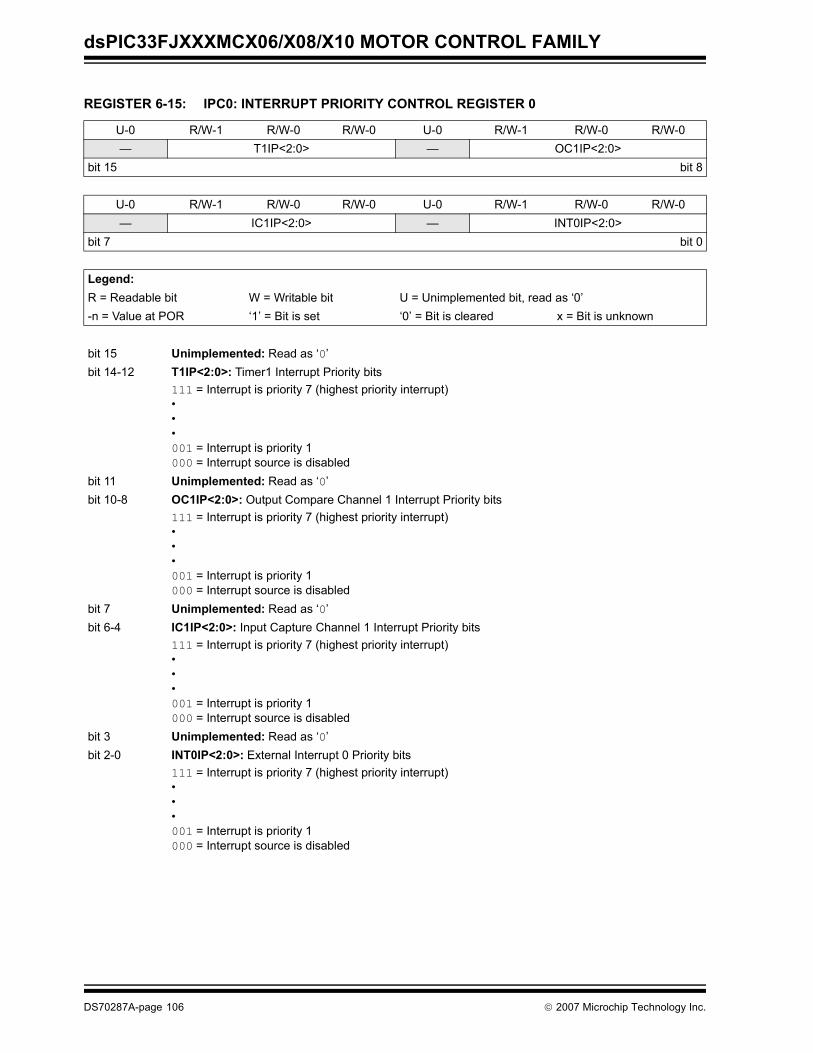
dsPIC33FJXXXMCX06/X08/X10 MOTOR CONTROL FAMILY
REGISTER 6-15: IPC0: INTERRUPT PRIORITY CONTROL REGISTER 0
U-0 R/W-1 R/W-0 R/W-0 U-0 R/W-1 R/W-0 R/W-0— T1IP<2:0> — OC1IP<2:0>
bit 15 bit 8
U-0 R/W-1 R/W-0 R/W-0 U-0 R/W-1 R/W-0 R/W-0— IC1IP<2:0> — INT0IP<2:0>
bit 7 bit 0
Legend:R = Readable bit W = Writable bit U = Unimplemented bit, read as ‘0’-n = Value at POR ‘1’ = Bit is set ‘0’ = Bit is cleared x = Bit is unknown
bit 15 Unimplemented: Read as ‘0’bit 14-12 T1IP<2:0>: Timer1 Interrupt Priority bits
111 = Interrupt is priority 7 (highest priority interrupt)•••001 = Interrupt is priority 1000 = Interrupt source is disabled
bit 11 Unimplemented: Read as ‘0’bit 10-8 OC1IP<2:0>: Output Compare Channel 1 Interrupt Priority bits
111 = Interrupt is priority 7 (highest priority interrupt)•••001 = Interrupt is priority 1000 = Interrupt source is disabled
bit 7 Unimplemented: Read as ‘0’bit 6-4 IC1IP<2:0>: Input Capture Channel 1 Interrupt Priority bits
111 = Interrupt is priority 7 (highest priority interrupt)•••001 = Interrupt is priority 1000 = Interrupt source is disabled
bit 3 Unimplemented: Read as ‘0’bit 2-0 INT0IP<2:0>: External Interrupt 0 Priority bits
111 = Interrupt is priority 7 (highest priority interrupt)•••001 = Interrupt is priority 1000 = Interrupt source is disabled
DS70287A-page 106 © 2007 Microchip Technology Inc.
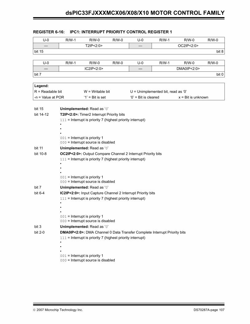
dsPIC33FJXXXMCX06/X08/X10 MOTOR CONTROL FAMILY
REGISTER 6-16: IPC1: INTERRUPT PRIORITY CONTROL REGISTER 1
U-0 R/W-1 R/W-0 R/W-0 U-0 R/W-1 R/W-0 R/W-0— T2IP<2:0> — OC2IP<2:0>
bit 15 bit 8
U-0 R/W-1 R/W-0 R/W-0 U-0 R/W-1 R/W-0 R/W-0— IC2IP<2:0> — DMA0IP<2:0>
bit 7 bit 0
Legend:R = Readable bit W = Writable bit U = Unimplemented bit, read as ‘0’-n = Value at POR ‘1’ = Bit is set ‘0’ = Bit is cleared x = Bit is unknown
bit 15 Unimplemented: Read as ‘0’bit 14-12 T2IP<2:0>: Timer2 Interrupt Priority bits
111 = Interrupt is priority 7 (highest priority interrupt)•••001 = Interrupt is priority 1000 = Interrupt source is disabled
bit 11 Unimplemented: Read as ‘0’bit 10-8 OC2IP<2:0>: Output Compare Channel 2 Interrupt Priority bits
111 = Interrupt is priority 7 (highest priority interrupt)•••001 = Interrupt is priority 1000 = Interrupt source is disabled
bit 7 Unimplemented: Read as ‘0’bit 6-4 IC2IP<2:0>: Input Capture Channel 2 Interrupt Priority bits
111 = Interrupt is priority 7 (highest priority interrupt)•••001 = Interrupt is priority 1000 = Interrupt source is disabled
bit 3 Unimplemented: Read as ‘0’bit 2-0 DMA0IP<2:0>: DMA Channel 0 Data Transfer Complete Interrupt Priority bits
111 = Interrupt is priority 7 (highest priority interrupt)•••001 = Interrupt is priority 1000 = Interrupt source is disabled
© 2007 Microchip Technology Inc. DS70287A-page 107
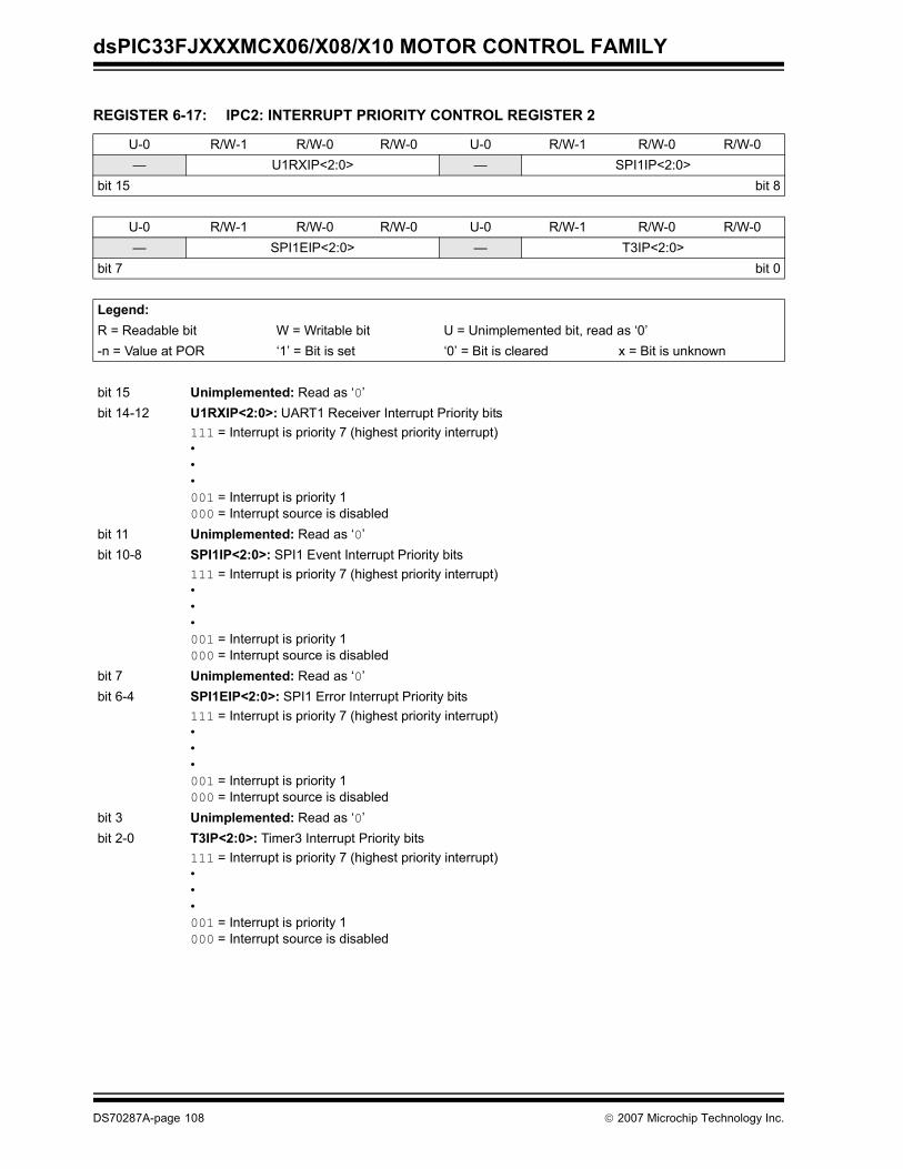
dsPIC33FJXXXMCX06/X08/X10 MOTOR CONTROL FAMILY
REGISTER 6-17: IPC2: INTERRUPT PRIORITY CONTROL REGISTER 2
U-0 R/W-1 R/W-0 R/W-0 U-0 R/W-1 R/W-0 R/W-0— U1RXIP<2:0> — SPI1IP<2:0>
bit 15 bit 8
U-0 R/W-1 R/W-0 R/W-0 U-0 R/W-1 R/W-0 R/W-0— SPI1EIP<2:0> — T3IP<2:0>
bit 7 bit 0
Legend:R = Readable bit W = Writable bit U = Unimplemented bit, read as ‘0’-n = Value at POR ‘1’ = Bit is set ‘0’ = Bit is cleared x = Bit is unknown
bit 15 Unimplemented: Read as ‘0’bit 14-12 U1RXIP<2:0>: UART1 Receiver Interrupt Priority bits
111 = Interrupt is priority 7 (highest priority interrupt)•••001 = Interrupt is priority 1000 = Interrupt source is disabled
bit 11 Unimplemented: Read as ‘0’bit 10-8 SPI1IP<2:0>: SPI1 Event Interrupt Priority bits
111 = Interrupt is priority 7 (highest priority interrupt)•••001 = Interrupt is priority 1000 = Interrupt source is disabled
bit 7 Unimplemented: Read as ‘0’bit 6-4 SPI1EIP<2:0>: SPI1 Error Interrupt Priority bits
111 = Interrupt is priority 7 (highest priority interrupt)•••001 = Interrupt is priority 1000 = Interrupt source is disabled
bit 3 Unimplemented: Read as ‘0’bit 2-0 T3IP<2:0>: Timer3 Interrupt Priority bits
111 = Interrupt is priority 7 (highest priority interrupt)•••001 = Interrupt is priority 1000 = Interrupt source is disabled
DS70287A-page 108 © 2007 Microchip Technology Inc.
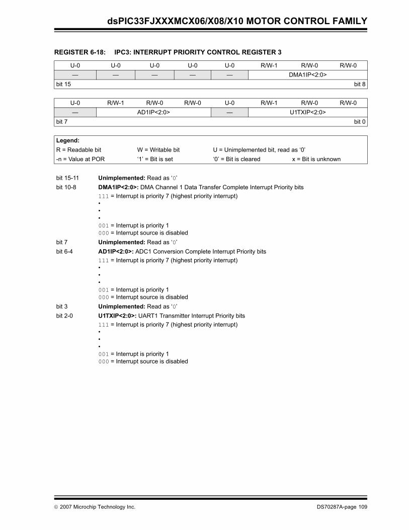
dsPIC33FJXXXMCX06/X08/X10 MOTOR CONTROL FAMILY
REGISTER 6-18: IPC3: INTERRUPT PRIORITY CONTROL REGISTER 3
U-0 U-0 U-0 U-0 U-0 R/W-1 R/W-0 R/W-0— — — — — DMA1IP<2:0>
bit 15 bit 8
U-0 R/W-1 R/W-0 R/W-0 U-0 R/W-1 R/W-0 R/W-0— AD1IP<2:0> — U1TXIP<2:0>
bit 7 bit 0
Legend:R = Readable bit W = Writable bit U = Unimplemented bit, read as ‘0’-n = Value at POR ‘1’ = Bit is set ‘0’ = Bit is cleared x = Bit is unknown
bit 15-11 Unimplemented: Read as ‘0’bit 10-8 DMA1IP<2:0>: DMA Channel 1 Data Transfer Complete Interrupt Priority bits
111 = Interrupt is priority 7 (highest priority interrupt)•••001 = Interrupt is priority 1000 = Interrupt source is disabled
bit 7 Unimplemented: Read as ‘0’bit 6-4 AD1IP<2:0>: ADC1 Conversion Complete Interrupt Priority bits
111 = Interrupt is priority 7 (highest priority interrupt)•••001 = Interrupt is priority 1000 = Interrupt source is disabled
bit 3 Unimplemented: Read as ‘0’bit 2-0 U1TXIP<2:0>: UART1 Transmitter Interrupt Priority bits
111 = Interrupt is priority 7 (highest priority interrupt)•••001 = Interrupt is priority 1000 = Interrupt source is disabled
© 2007 Microchip Technology Inc. DS70287A-page 109
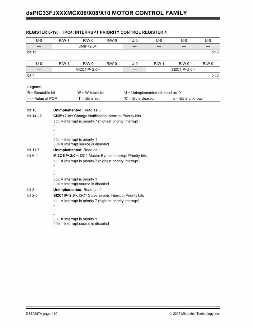
dsPIC33FJXXXMCX06/X08/X10 MOTOR CONTROL FAMILY
REGISTER 6-19: IPC4: INTERRUPT PRIORITY CONTROL REGISTER 4
U-0 R/W-1 R/W-0 R/W-0 U-0 U-0 U-0 U-0— CNIP<2:0> — — — —
bit 15 bit 8
U-0 R/W-1 R/W-0 R/W-0 U-0 R/W-1 R/W-0 R/W-0— MI2C1IP<2:0> — SI2C1IP<2:0>
bit 7 bit 0
Legend:R = Readable bit W = Writable bit U = Unimplemented bit, read as ‘0’-n = Value at POR ‘1’ = Bit is set ‘0’ = Bit is cleared x = Bit is unknown
bit 15 Unimplemented: Read as ‘0’bit 14-12 CNIP<2:0>: Change Notification Interrupt Priority bits
111 = Interrupt is priority 7 (highest priority interrupt)•••001 = Interrupt is priority 1000 = Interrupt source is disabled
bit 11-7 Unimplemented: Read as ‘0’bit 6-4 MI2C1IP<2:0>: I2C1 Master Events Interrupt Priority bits
111 = Interrupt is priority 7 (highest priority interrupt)•••001 = Interrupt is priority 1000 = Interrupt source is disabled
bit 3 Unimplemented: Read as ‘0’bit 2-0 SI2C1IP<2:0>: I2C1 Slave Events Interrupt Priority bits
111 = Interrupt is priority 7 (highest priority interrupt)•••001 = Interrupt is priority 1000 = Interrupt source is disabled
DS70287A-page 110 © 2007 Microchip Technology Inc.
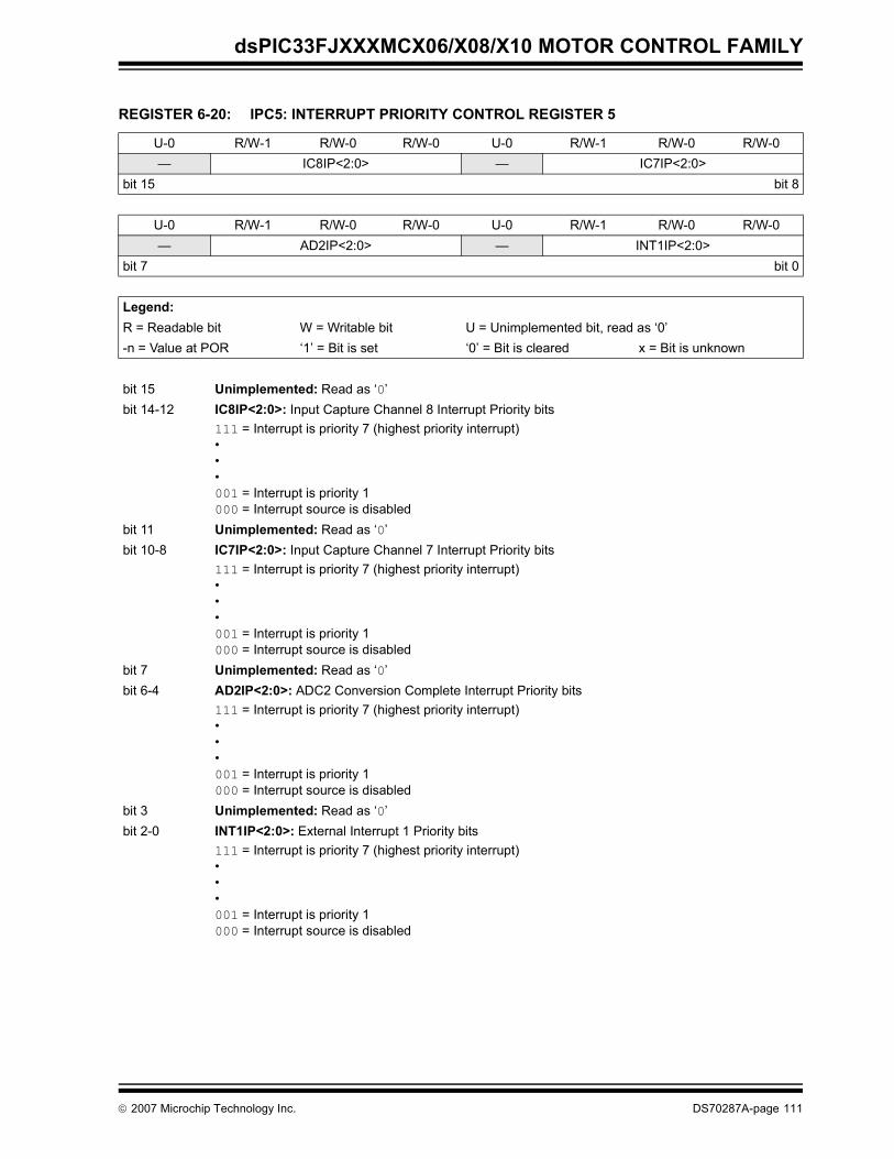
dsPIC33FJXXXMCX06/X08/X10 MOTOR CONTROL FAMILY
REGISTER 6-20: IPC5: INTERRUPT PRIORITY CONTROL REGISTER 5
U-0 R/W-1 R/W-0 R/W-0 U-0 R/W-1 R/W-0 R/W-0— IC8IP<2:0> — IC7IP<2:0>
bit 15 bit 8
U-0 R/W-1 R/W-0 R/W-0 U-0 R/W-1 R/W-0 R/W-0— AD2IP<2:0> — INT1IP<2:0>
bit 7 bit 0
Legend:R = Readable bit W = Writable bit U = Unimplemented bit, read as ‘0’-n = Value at POR ‘1’ = Bit is set ‘0’ = Bit is cleared x = Bit is unknown
bit 15 Unimplemented: Read as ‘0’bit 14-12 IC8IP<2:0>: Input Capture Channel 8 Interrupt Priority bits
111 = Interrupt is priority 7 (highest priority interrupt)•••001 = Interrupt is priority 1000 = Interrupt source is disabled
bit 11 Unimplemented: Read as ‘0’bit 10-8 IC7IP<2:0>: Input Capture Channel 7 Interrupt Priority bits
111 = Interrupt is priority 7 (highest priority interrupt)•••001 = Interrupt is priority 1000 = Interrupt source is disabled
bit 7 Unimplemented: Read as ‘0’bit 6-4 AD2IP<2:0>: ADC2 Conversion Complete Interrupt Priority bits
111 = Interrupt is priority 7 (highest priority interrupt)•••001 = Interrupt is priority 1000 = Interrupt source is disabled
bit 3 Unimplemented: Read as ‘0’bit 2-0 INT1IP<2:0>: External Interrupt 1 Priority bits
111 = Interrupt is priority 7 (highest priority interrupt)•••001 = Interrupt is priority 1000 = Interrupt source is disabled
© 2007 Microchip Technology Inc. DS70287A-page 111
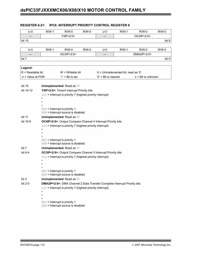
dsPIC33FJXXXMCX06/X08/X10 MOTOR CONTROL FAMILY
REGISTER 6-21: IPC6: INTERRUPT PRIORITY CONTROL REGISTER 6
U-0 R/W-1 R/W-0 R/W-0 U-0 R/W-1 R/W-0 R/W-0— T4IP<2:0> — OC4IP<2:0>
bit 15 bit 8
U-0 R/W-1 R/W-0 R/W-0 U-0 R/W-1 R/W-0 R/W-0— OC3IP<2:0> — DMA2IP<2:0>
bit 7 bit 0
Legend:R = Readable bit W = Writable bit U = Unimplemented bit, read as ‘0’-n = Value at POR ‘1’ = Bit is set ‘0’ = Bit is cleared x = Bit is unknown
bit 15 Unimplemented: Read as ‘0’bit 14-12 T4IP<2:0>: Timer4 Interrupt Priority bits
111 = Interrupt is priority 7 (highest priority interrupt)•••001 = Interrupt is priority 1000 = Interrupt source is disabled
bit 11 Unimplemented: Read as ‘0’bit 10-8 OC4IP<2:0>: Output Compare Channel 4 Interrupt Priority bits
111 = Interrupt is priority 7 (highest priority interrupt)•••001 = Interrupt is priority 1000 = Interrupt source is disabled
bit 7 Unimplemented: Read as ‘0’bit 6-4 OC3IP<2:0>: Output Compare Channel 3 Interrupt Priority bits
111 = Interrupt is priority 7 (highest priority interrupt)•••001 = Interrupt is priority 1000 = Interrupt source is disabled
bit 3 Unimplemented: Read as ‘0’bit 2-0 DMA2IP<2:0>: DMA Channel 2 Data Transfer Complete Interrupt Priority bits
111 = Interrupt is priority 7 (highest priority interrupt)•••001 = Interrupt is priority 1000 = Interrupt source is disabled
DS70287A-page 112 © 2007 Microchip Technology Inc.

dsPIC33FJXXXMCX06/X08/X10 MOTOR CONTROL FAMILY
REGISTER 6-22: IPC7: INTERRUPT PRIORITY CONTROL REGISTER 7
U-0 R/W-1 R/W-0 R/W-0 U-0 R/W-1 R/W-0 R/W-0— U2TXIP<2:0> — U2RXIP<2:0>
bit 15 bit 8
U-0 R/W-1 R/W-0 R/W-0 U-0 R/W-1 R/W-0 R/W-0— INT2IP<2:0> — T5IP<2:0>
bit 7 bit 0
Legend:R = Readable bit W = Writable bit U = Unimplemented bit, read as ‘0’-n = Value at POR ‘1’ = Bit is set ‘0’ = Bit is cleared x = Bit is unknown
bit 15 Unimplemented: Read as ‘0’bit 14-12 U2TXIP<2:0>: UART2 Transmitter Interrupt Priority bits
111 = Interrupt is priority 7 (highest priority interrupt)•••001 = Interrupt is priority 1000 = Interrupt source is disabled
bit 11 Unimplemented: Read as ‘0’bit 10-8 U2RXIP<2:0>: UART2 Receiver Interrupt Priority bits
111 = Interrupt is priority 7 (highest priority interrupt)•••001 = Interrupt is priority 1000 = Interrupt source is disabled
bit 7 Unimplemented: Read as ‘0’bit 6-4 INT2IP<2:0>: External Interrupt 2 Priority bits
111 = Interrupt is priority 7 (highest priority interrupt)•••001 = Interrupt is priority 1000 = Interrupt source is disabled
bit 3 Unimplemented: Read as ‘0’bit 2-0 T5IP<2:0>: Timer5 Interrupt Priority bits
111 = Interrupt is priority 7 (highest priority interrupt)•••001 = Interrupt is priority 1000 = Interrupt source is disabled
© 2007 Microchip Technology Inc. DS70287A-page 113
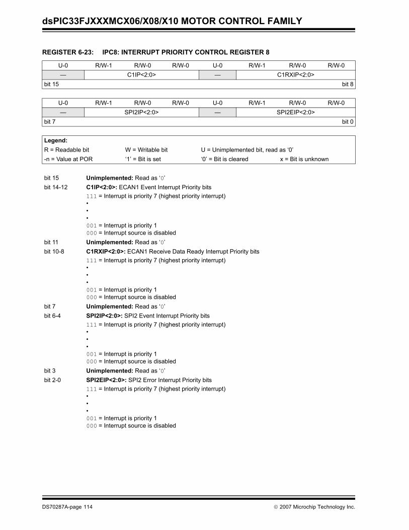
dsPIC33FJXXXMCX06/X08/X10 MOTOR CONTROL FAMILY
REGISTER 6-23: IPC8: INTERRUPT PRIORITY CONTROL REGISTER 8
U-0 R/W-1 R/W-0 R/W-0 U-0 R/W-1 R/W-0 R/W-0— C1IP<2:0> — C1RXIP<2:0>
bit 15 bit 8
U-0 R/W-1 R/W-0 R/W-0 U-0 R/W-1 R/W-0 R/W-0— SPI2IP<2:0> — SPI2EIP<2:0>
bit 7 bit 0
Legend:R = Readable bit W = Writable bit U = Unimplemented bit, read as ‘0’-n = Value at POR ‘1’ = Bit is set ‘0’ = Bit is cleared x = Bit is unknown
bit 15 Unimplemented: Read as ‘0’bit 14-12 C1IP<2:0>: ECAN1 Event Interrupt Priority bits
111 = Interrupt is priority 7 (highest priority interrupt)•••001 = Interrupt is priority 1000 = Interrupt source is disabled
bit 11 Unimplemented: Read as ‘0’bit 10-8 C1RXIP<2:0>: ECAN1 Receive Data Ready Interrupt Priority bits
111 = Interrupt is priority 7 (highest priority interrupt)•••001 = Interrupt is priority 1000 = Interrupt source is disabled
bit 7 Unimplemented: Read as ‘0’bit 6-4 SPI2IP<2:0>: SPI2 Event Interrupt Priority bits
111 = Interrupt is priority 7 (highest priority interrupt)•••001 = Interrupt is priority 1000 = Interrupt source is disabled
bit 3 Unimplemented: Read as ‘0’bit 2-0 SPI2EIP<2:0>: SPI2 Error Interrupt Priority bits
111 = Interrupt is priority 7 (highest priority interrupt)•••001 = Interrupt is priority 1000 = Interrupt source is disabled
DS70287A-page 114 © 2007 Microchip Technology Inc.
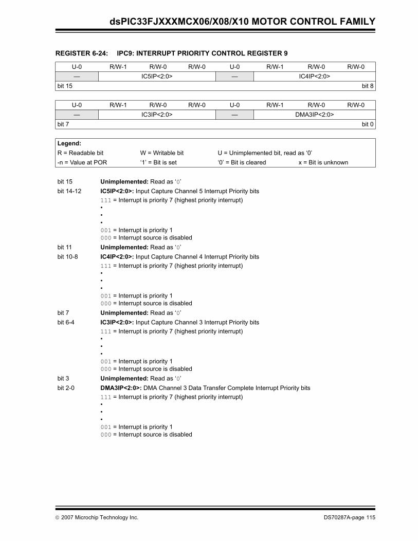
dsPIC33FJXXXMCX06/X08/X10 MOTOR CONTROL FAMILY
REGISTER 6-24: IPC9: INTERRUPT PRIORITY CONTROL REGISTER 9
U-0 R/W-1 R/W-0 R/W-0 U-0 R/W-1 R/W-0 R/W-0— IC5IP<2:0> — IC4IP<2:0>
bit 15 bit 8
U-0 R/W-1 R/W-0 R/W-0 U-0 R/W-1 R/W-0 R/W-0— IC3IP<2:0> — DMA3IP<2:0>
bit 7 bit 0
Legend:R = Readable bit W = Writable bit U = Unimplemented bit, read as ‘0’-n = Value at POR ‘1’ = Bit is set ‘0’ = Bit is cleared x = Bit is unknown
bit 15 Unimplemented: Read as ‘0’bit 14-12 IC5IP<2:0>: Input Capture Channel 5 Interrupt Priority bits
111 = Interrupt is priority 7 (highest priority interrupt)•••001 = Interrupt is priority 1000 = Interrupt source is disabled
bit 11 Unimplemented: Read as ‘0’bit 10-8 IC4IP<2:0>: Input Capture Channel 4 Interrupt Priority bits
111 = Interrupt is priority 7 (highest priority interrupt)•••001 = Interrupt is priority 1000 = Interrupt source is disabled
bit 7 Unimplemented: Read as ‘0’bit 6-4 IC3IP<2:0>: Input Capture Channel 3 Interrupt Priority bits
111 = Interrupt is priority 7 (highest priority interrupt)•••001 = Interrupt is priority 1000 = Interrupt source is disabled
bit 3 Unimplemented: Read as ‘0’bit 2-0 DMA3IP<2:0>: DMA Channel 3 Data Transfer Complete Interrupt Priority bits
111 = Interrupt is priority 7 (highest priority interrupt)•••001 = Interrupt is priority 1000 = Interrupt source is disabled
© 2007 Microchip Technology Inc. DS70287A-page 115
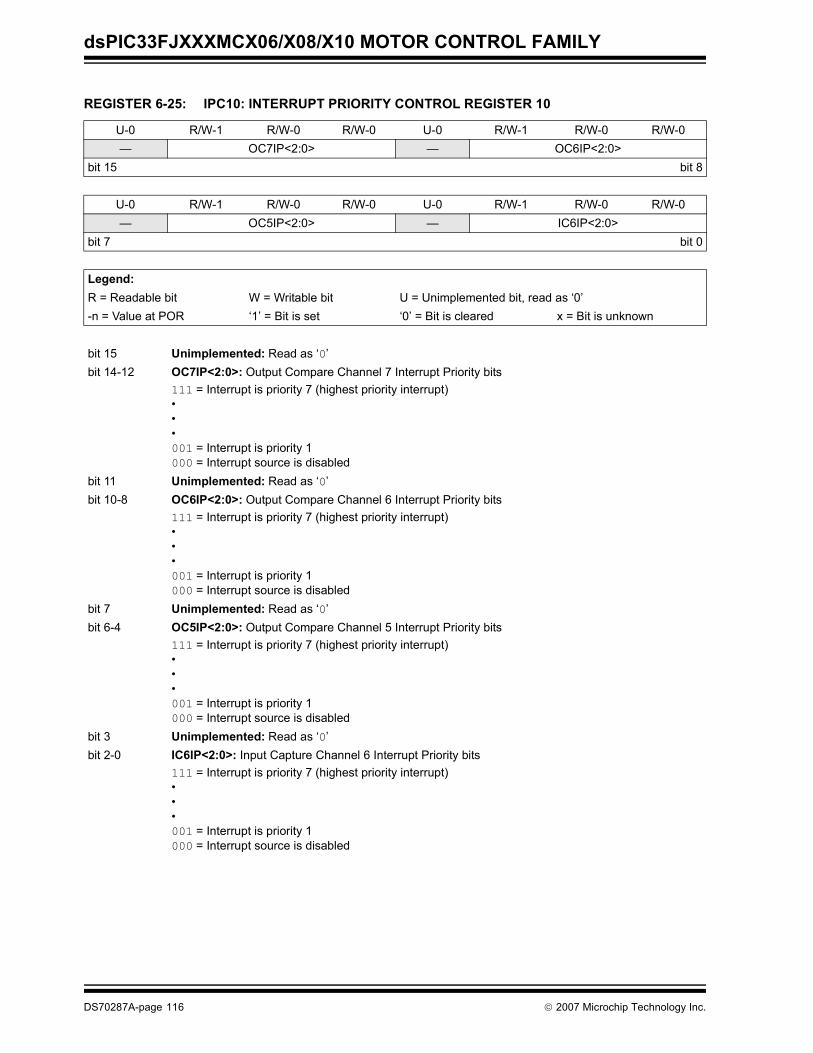
dsPIC33FJXXXMCX06/X08/X10 MOTOR CONTROL FAMILY
REGISTER 6-25: IPC10: INTERRUPT PRIORITY CONTROL REGISTER 10
U-0 R/W-1 R/W-0 R/W-0 U-0 R/W-1 R/W-0 R/W-0— OC7IP<2:0> — OC6IP<2:0>
bit 15 bit 8
U-0 R/W-1 R/W-0 R/W-0 U-0 R/W-1 R/W-0 R/W-0— OC5IP<2:0> — IC6IP<2:0>
bit 7 bit 0
Legend:R = Readable bit W = Writable bit U = Unimplemented bit, read as ‘0’-n = Value at POR ‘1’ = Bit is set ‘0’ = Bit is cleared x = Bit is unknown
bit 15 Unimplemented: Read as ‘0’bit 14-12 OC7IP<2:0>: Output Compare Channel 7 Interrupt Priority bits
111 = Interrupt is priority 7 (highest priority interrupt)•••001 = Interrupt is priority 1000 = Interrupt source is disabled
bit 11 Unimplemented: Read as ‘0’bit 10-8 OC6IP<2:0>: Output Compare Channel 6 Interrupt Priority bits
111 = Interrupt is priority 7 (highest priority interrupt)•••001 = Interrupt is priority 1000 = Interrupt source is disabled
bit 7 Unimplemented: Read as ‘0’bit 6-4 OC5IP<2:0>: Output Compare Channel 5 Interrupt Priority bits
111 = Interrupt is priority 7 (highest priority interrupt)•••001 = Interrupt is priority 1000 = Interrupt source is disabled
bit 3 Unimplemented: Read as ‘0’bit 2-0 IC6IP<2:0>: Input Capture Channel 6 Interrupt Priority bits
111 = Interrupt is priority 7 (highest priority interrupt)•••001 = Interrupt is priority 1000 = Interrupt source is disabled
DS70287A-page 116 © 2007 Microchip Technology Inc.
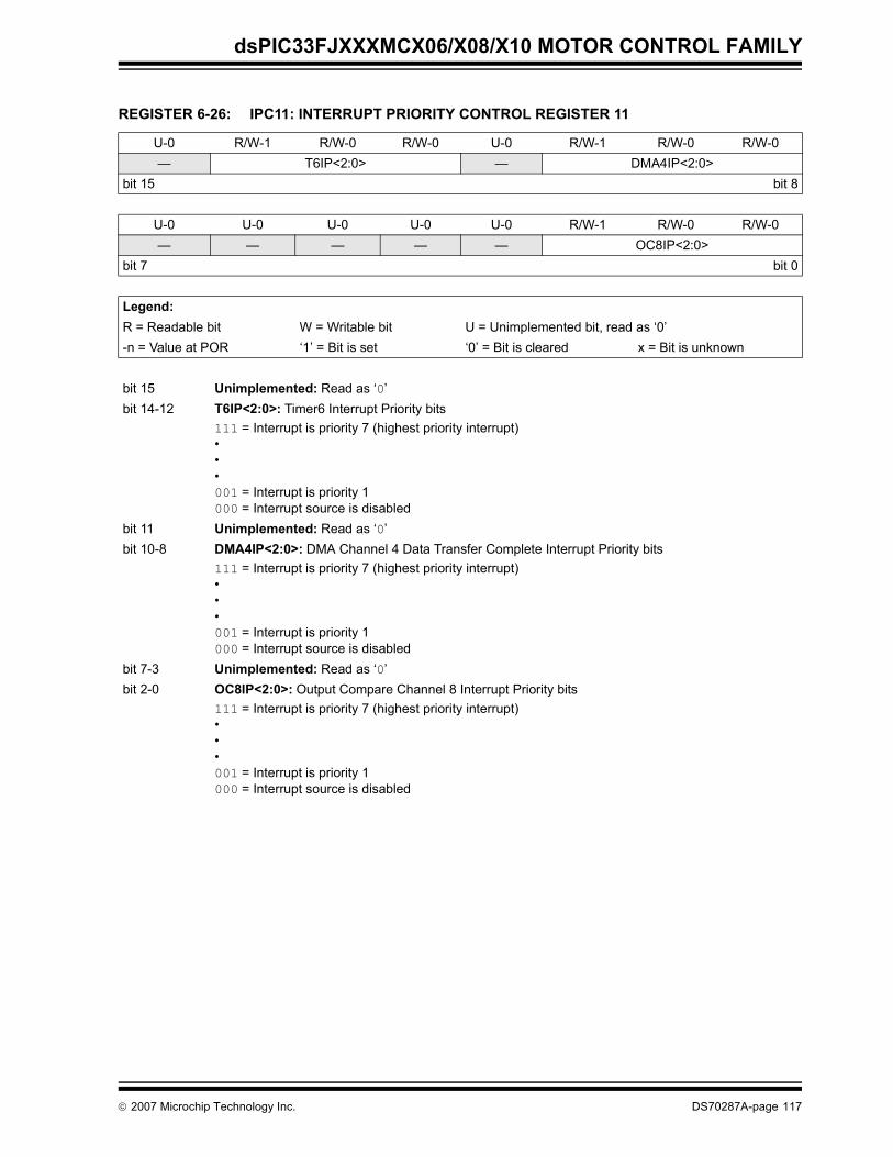
dsPIC33FJXXXMCX06/X08/X10 MOTOR CONTROL FAMILY
REGISTER 6-26: IPC11: INTERRUPT PRIORITY CONTROL REGISTER 11
U-0 R/W-1 R/W-0 R/W-0 U-0 R/W-1 R/W-0 R/W-0— T6IP<2:0> — DMA4IP<2:0>
bit 15 bit 8
U-0 U-0 U-0 U-0 U-0 R/W-1 R/W-0 R/W-0— — — — — OC8IP<2:0>
bit 7 bit 0
Legend:R = Readable bit W = Writable bit U = Unimplemented bit, read as ‘0’-n = Value at POR ‘1’ = Bit is set ‘0’ = Bit is cleared x = Bit is unknown
bit 15 Unimplemented: Read as ‘0’bit 14-12 T6IP<2:0>: Timer6 Interrupt Priority bits
111 = Interrupt is priority 7 (highest priority interrupt)•••001 = Interrupt is priority 1000 = Interrupt source is disabled
bit 11 Unimplemented: Read as ‘0’bit 10-8 DMA4IP<2:0>: DMA Channel 4 Data Transfer Complete Interrupt Priority bits
111 = Interrupt is priority 7 (highest priority interrupt)•••001 = Interrupt is priority 1000 = Interrupt source is disabled
bit 7-3 Unimplemented: Read as ‘0’bit 2-0 OC8IP<2:0>: Output Compare Channel 8 Interrupt Priority bits
111 = Interrupt is priority 7 (highest priority interrupt)•••001 = Interrupt is priority 1000 = Interrupt source is disabled
© 2007 Microchip Technology Inc. DS70287A-page 117
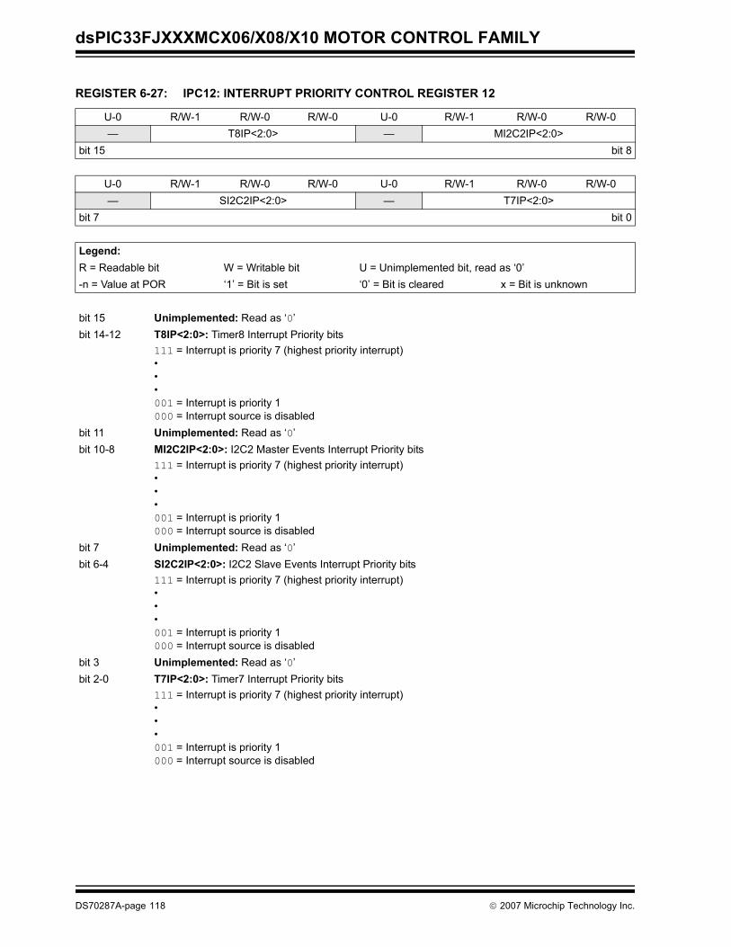
dsPIC33FJXXXMCX06/X08/X10 MOTOR CONTROL FAMILY
REGISTER 6-27: IPC12: INTERRUPT PRIORITY CONTROL REGISTER 12
U-0 R/W-1 R/W-0 R/W-0 U-0 R/W-1 R/W-0 R/W-0— T8IP<2:0> — MI2C2IP<2:0>
bit 15 bit 8
U-0 R/W-1 R/W-0 R/W-0 U-0 R/W-1 R/W-0 R/W-0— SI2C2IP<2:0> — T7IP<2:0>
bit 7 bit 0
Legend:R = Readable bit W = Writable bit U = Unimplemented bit, read as ‘0’-n = Value at POR ‘1’ = Bit is set ‘0’ = Bit is cleared x = Bit is unknown
bit 15 Unimplemented: Read as ‘0’bit 14-12 T8IP<2:0>: Timer8 Interrupt Priority bits
111 = Interrupt is priority 7 (highest priority interrupt)•••001 = Interrupt is priority 1000 = Interrupt source is disabled
bit 11 Unimplemented: Read as ‘0’bit 10-8 MI2C2IP<2:0>: I2C2 Master Events Interrupt Priority bits
111 = Interrupt is priority 7 (highest priority interrupt)•••001 = Interrupt is priority 1000 = Interrupt source is disabled
bit 7 Unimplemented: Read as ‘0’bit 6-4 SI2C2IP<2:0>: I2C2 Slave Events Interrupt Priority bits
111 = Interrupt is priority 7 (highest priority interrupt)•••001 = Interrupt is priority 1000 = Interrupt source is disabled
bit 3 Unimplemented: Read as ‘0’bit 2-0 T7IP<2:0>: Timer7 Interrupt Priority bits
111 = Interrupt is priority 7 (highest priority interrupt)•••001 = Interrupt is priority 1000 = Interrupt source is disabled
DS70287A-page 118 © 2007 Microchip Technology Inc.
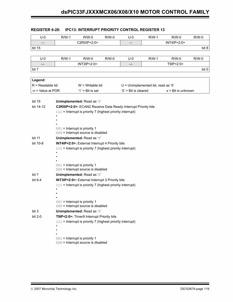
dsPIC33FJXXXMCX06/X08/X10 MOTOR CONTROL FAMILY
REGISTER 6-28: IPC13: INTERRUPT PRIORITY CONTROL REGISTER 13
U-0 R/W-1 R/W-0 R/W-0 U-0 R/W-1 R/W-0 R/W-0— C2RXIP<2:0> — INT4IP<2:0>
bit 15 bit 8
U-0 R/W-1 R/W-0 R/W-0 U-0 R/W-1 R/W-0 R/W-0— INT3IP<2:0> — T9IP<2:0>
bit 7 bit 0
Legend:R = Readable bit W = Writable bit U = Unimplemented bit, read as ‘0’-n = Value at POR ‘1’ = Bit is set ‘0’ = Bit is cleared x = Bit is unknown
bit 15 Unimplemented: Read as ‘0’bit 14-12 C2RXIP<2:0>: ECAN2 Receive Data Ready Interrupt Priority bits
111 = Interrupt is priority 7 (highest priority interrupt)•••001 = Interrupt is priority 1000 = Interrupt source is disabled
bit 11 Unimplemented: Read as ‘0’bit 10-8 INT4IP<2:0>: External Interrupt 4 Priority bits
111 = Interrupt is priority 7 (highest priority interrupt)•••001 = Interrupt is priority 1000 = Interrupt source is disabled
bit 7 Unimplemented: Read as ‘0’bit 6-4 INT3IP<2:0>: External Interrupt 3 Priority bits
111 = Interrupt is priority 7 (highest priority interrupt)•••001 = Interrupt is priority 1000 = Interrupt source is disabled
bit 3 Unimplemented: Read as ‘0’bit 2-0 T9IP<2:0>: Timer9 Interrupt Priority bits
111 = Interrupt is priority 7 (highest priority interrupt)•••001 = Interrupt is priority 1000 = Interrupt source is disabled
© 2007 Microchip Technology Inc. DS70287A-page 119

dsPIC33FJXXXMCX06/X08/X10 MOTOR CONTROL FAMILY
REGISTER 6-29: IPC14: INTERRUPT PRIORITY CONTROL REGISTER 14
U-0 R/W-1 R/W-0 R/W-0 U-0 R/W-1 R/W-0 R/W-0— — — — — QEIIP<2:0>
bit 15 bit 8
U-0 R/W-1 R/W-0 R/W-0 U-0 R/W-1 R/W-0 R/W-0— PWMIP<2:0> — C2IP<2:0>
bit 7 bit 0
Legend:R = Readable bit W = Writable bit U = Unimplemented bit, read as ‘0’-n = Value at POR ‘1’ = Bit is set ‘0’ = Bit is cleared x = Bit is unknown
bit 15-11 Unimplemented: Read as ‘0’bit 10-8 QEIIP<2:0>: QEI Interrupt Priority bits
111 = Interrupt is priority 7 (highest priority interrupt)•••001 = Interrupt is priority 1000 = Interrupt source is disabled
bit 7 Unimplemented: Read as ‘0’bit 6-4 PWMIP<2:0>: PWM Interrupt Priority bits
111 = Interrupt is priority 7 (highest priority interrupt)•••001 = Interrupt is priority 1000 = Interrupt source is disabled
bit 3 Unimplemented: Read as ‘0’bit 2-0 C2IP<2:0>: ECAN2 Event Interrupt Priority bits
111 = Interrupt is priority 7 (highest priority interrupt)•••001 = Interrupt is priority 1000 = Interrupt source is disabled
DS70287A-page 120 © 2007 Microchip Technology Inc.
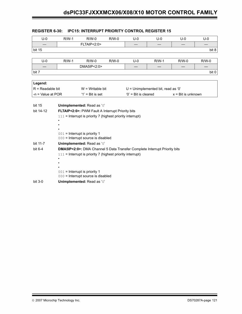
dsPIC33FJXXXMCX06/X08/X10 MOTOR CONTROL FAMILY
REGISTER 6-30: IPC15: INTERRUPT PRIORITY CONTROL REGISTER 15
U-0 R/W-1 R/W-0 R/W-0 U-0 U-0 U-0 U-0— FLTAIP<2:0> — — — —
bit 15 bit 8
U-0 R/W-1 R/W-0 R/W-0 U-0 R/W-1 R/W-0 R/W-0— DMA5IP<2:0> — — — —
bit 7 bit 0
Legend:R = Readable bit W = Writable bit U = Unimplemented bit, read as ‘0’-n = Value at POR ‘1’ = Bit is set ‘0’ = Bit is cleared x = Bit is unknown
bit 15 Unimplemented: Read as ‘0’bit 14-12 FLTAIP<2:0>: PWM Fault A Interrupt Priority bits
111 = Interrupt is priority 7 (highest priority interrupt)•••001 = Interrupt is priority 1000 = Interrupt source is disabled
bit 11-7 Unimplemented: Read as ‘0’bit 6-4 DMA5IP<2:0>: DMA Channel 5 Data Transfer Complete Interrupt Priority bits
111 = Interrupt is priority 7 (highest priority interrupt)•••001 = Interrupt is priority 1000 = Interrupt source is disabled
bit 3-0 Unimplemented: Read as ‘0’
© 2007 Microchip Technology Inc. DS70287A-page 121
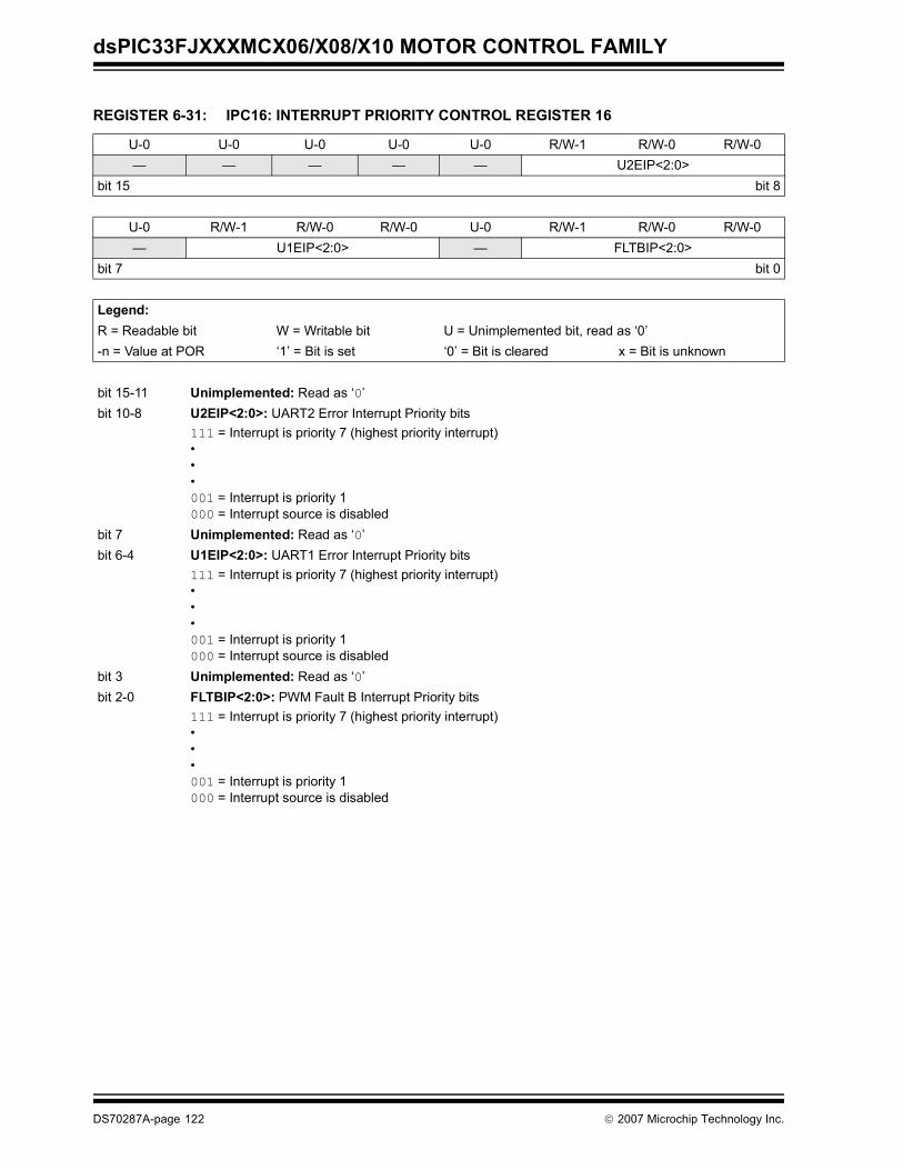
dsPIC33FJXXXMCX06/X08/X10 MOTOR CONTROL FAMILY
REGISTER 6-31: IPC16: INTERRUPT PRIORITY CONTROL REGISTER 16
U-0 U-0 U-0 U-0 U-0 R/W-1 R/W-0 R/W-0— — — — — U2EIP<2:0>
bit 15 bit 8
U-0 R/W-1 R/W-0 R/W-0 U-0 R/W-1 R/W-0 R/W-0— U1EIP<2:0> — FLTBIP<2:0>
bit 7 bit 0
Legend:R = Readable bit W = Writable bit U = Unimplemented bit, read as ‘0’-n = Value at POR ‘1’ = Bit is set ‘0’ = Bit is cleared x = Bit is unknown
bit 15-11 Unimplemented: Read as ‘0’bit 10-8 U2EIP<2:0>: UART2 Error Interrupt Priority bits
111 = Interrupt is priority 7 (highest priority interrupt)•••001 = Interrupt is priority 1000 = Interrupt source is disabled
bit 7 Unimplemented: Read as ‘0’bit 6-4 U1EIP<2:0>: UART1 Error Interrupt Priority bits
111 = Interrupt is priority 7 (highest priority interrupt)•••001 = Interrupt is priority 1000 = Interrupt source is disabled
bit 3 Unimplemented: Read as ‘0’bit 2-0 FLTBIP<2:0>: PWM Fault B Interrupt Priority bits
111 = Interrupt is priority 7 (highest priority interrupt)•••001 = Interrupt is priority 1000 = Interrupt source is disabled
DS70287A-page 122 © 2007 Microchip Technology Inc.
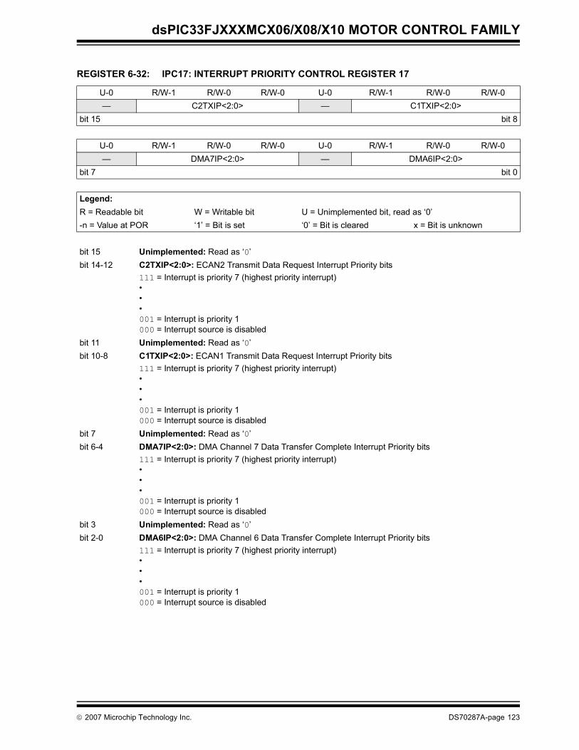
dsPIC33FJXXXMCX06/X08/X10 MOTOR CONTROL FAMILY
REGISTER 6-32: IPC17: INTERRUPT PRIORITY CONTROL REGISTER 17
U-0 R/W-1 R/W-0 R/W-0 U-0 R/W-1 R/W-0 R/W-0— C2TXIP<2:0> — C1TXIP<2:0>
bit 15 bit 8
U-0 R/W-1 R/W-0 R/W-0 U-0 R/W-1 R/W-0 R/W-0— DMA7IP<2:0> — DMA6IP<2:0>
bit 7 bit 0
Legend:R = Readable bit W = Writable bit U = Unimplemented bit, read as ‘0’-n = Value at POR ‘1’ = Bit is set ‘0’ = Bit is cleared x = Bit is unknown
bit 15 Unimplemented: Read as ‘0’bit 14-12 C2TXIP<2:0>: ECAN2 Transmit Data Request Interrupt Priority bits
111 = Interrupt is priority 7 (highest priority interrupt)•••001 = Interrupt is priority 1000 = Interrupt source is disabled
bit 11 Unimplemented: Read as ‘0’bit 10-8 C1TXIP<2:0>: ECAN1 Transmit Data Request Interrupt Priority bits
111 = Interrupt is priority 7 (highest priority interrupt)•••001 = Interrupt is priority 1000 = Interrupt source is disabled
bit 7 Unimplemented: Read as ‘0’bit 6-4 DMA7IP<2:0>: DMA Channel 7 Data Transfer Complete Interrupt Priority bits
111 = Interrupt is priority 7 (highest priority interrupt)•••001 = Interrupt is priority 1000 = Interrupt source is disabled
bit 3 Unimplemented: Read as ‘0’bit 2-0 DMA6IP<2:0>: DMA Channel 6 Data Transfer Complete Interrupt Priority bits
111 = Interrupt is priority 7 (highest priority interrupt)•••001 = Interrupt is priority 1000 = Interrupt source is disabled
© 2007 Microchip Technology Inc. DS70287A-page 123
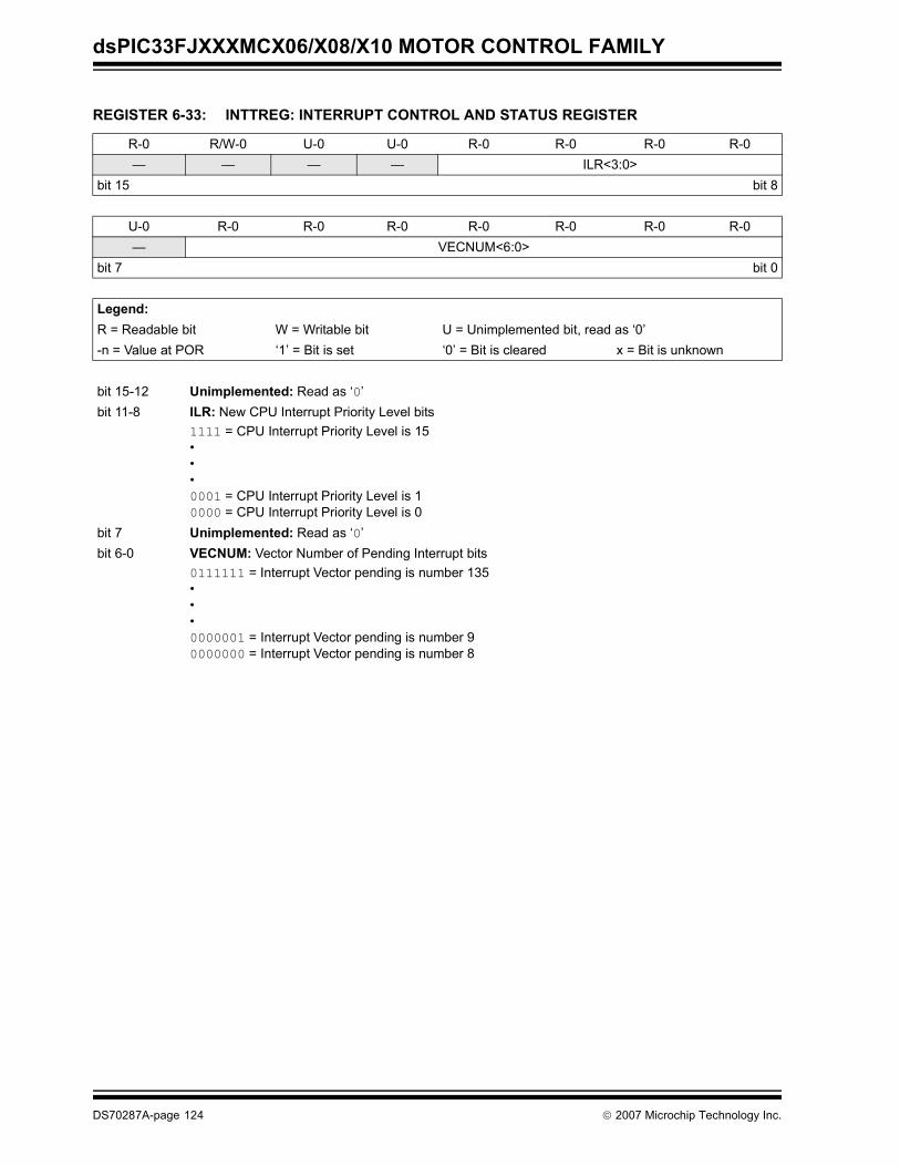
dsPIC33FJXXXMCX06/X08/X10 MOTOR CONTROL FAMILY
REGISTER 6-33: INTTREG: INTERRUPT CONTROL AND STATUS REGISTER
R-0 R/W-0 U-0 U-0 R-0 R-0 R-0 R-0— — — — ILR<3:0>
bit 15 bit 8
U-0 R-0 R-0 R-0 R-0 R-0 R-0 R-0— VECNUM<6:0>
bit 7 bit 0
Legend:R = Readable bit W = Writable bit U = Unimplemented bit, read as ‘0’-n = Value at POR ‘1’ = Bit is set ‘0’ = Bit is cleared x = Bit is unknown
bit 15-12 Unimplemented: Read as ‘0’bit 11-8 ILR: New CPU Interrupt Priority Level bits
1111 = CPU Interrupt Priority Level is 15 •••0001 = CPU Interrupt Priority Level is 10000 = CPU Interrupt Priority Level is 0
bit 7 Unimplemented: Read as ‘0’bit 6-0 VECNUM: Vector Number of Pending Interrupt bits
0111111 = Interrupt Vector pending is number 135 •••0000001 = Interrupt Vector pending is number 90000000 = Interrupt Vector pending is number 8
DS70287A-page 124 © 2007 Microchip Technology Inc.
dsPIC33FJXXXMCX06/X08/X10 MOTOR CONTROL FAMILY
6.4 Interrupt Setup Procedures
6.4.1 INITIALIZATIONTo configure an interrupt source, do the following:
1. Set the NSTDIS bit (INTCON1<15>) if nestedinterrupts are not desired.
2. Select the user-assigned priority level for theinterrupt source by writing the control bits in theappropriate IPCx register. The priority level willdepend on the specific application and type ofinterrupt source. If multiple priority levels are notdesired, the IPCx register control bits for allenabled interrupt sources may be programmedto the same non-zero value.
3. Clear the interrupt flag status bit associated withthe peripheral in the associated IFSx register.
4. Enable the interrupt source by setting the inter-rupt enable control bit associated with thesource in the appropriate IECx register.
6.4.2 INTERRUPT SERVICE ROUTINEThe method that is used to declare an ISR and initializethe IVT with the correct vector address will depend onthe programming language (i.e., C or assembler) andthe language development tool suite that is used todevelop the application. In general, the user must clearthe interrupt flag in the appropriate IFSx register for thesource of interrupt that the ISR handles. Otherwise, theISR will be re-entered immediately after exiting theroutine. If the ISR is coded in assembly language, itmust be terminated using a RETFIE instruction tounstack the saved PC value, SRL value and old CPUpriority level.
6.4.3 TRAP SERVICE ROUTINEA Trap Service Routine (TSR) is coded like an ISR,except that the appropriate trap status flag in theINTCON1 register must be cleared to avoid re-entryinto the TSR.
6.4.4 INTERRUPT DISABLEAll user interrupts can be disabled using the followingprocedure:
1. Push the current SR value onto the softwarestack using the PUSH instruction.
2. Force the CPU to priority level 7 by inclusiveORing the value OEh with SRL.
To enable user interrupts, the POP instruction may beused to restore the previous SR value.
Note that only user interrupts with a priority level of 7 orless can be disabled. Trap sources (level 8-level 15)cannot be disabled.
The DISI instruction provides a convenient way to dis-able interrupts of priority levels 1-6 for a fixed period oftime. Level 7 interrupt sources are not disabled by theDISI instruction.
Note: At a device Reset, the IPCx registers areinitialized such that all user interruptsources are assigned to priority level 4.
© 2007 Microchip Technology Inc. DS70287A-page 125

dsPIC33FJXXXMCX06/X08/X10 MOTOR CONTROL FAMILY
NOTES:
DS70287A-page 126 © 2007 Microchip Technology Inc.
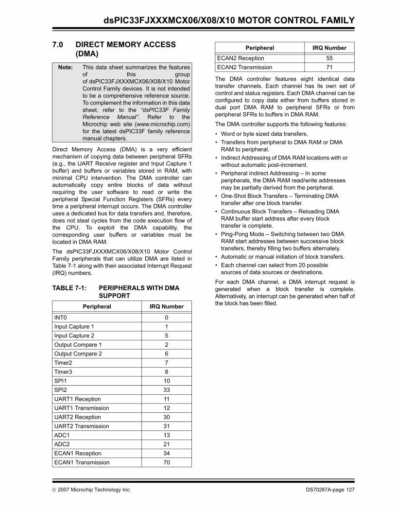
dsPIC33FJXXXMCX06/X08/X10 MOTOR CONTROL FAMILY
7.0 DIRECT MEMORY ACCESS (DMA)
Direct Memory Access (DMA) is a very efficientmechanism of copying data between peripheral SFRs(e.g., the UART Receive register and Input Capture 1buffer) and buffers or variables stored in RAM, withminimal CPU intervention. The DMA controller canautomatically copy entire blocks of data withoutrequiring the user software to read or write theperipheral Special Function Registers (SFRs) everytime a peripheral interrupt occurs. The DMA controlleruses a dedicated bus for data transfers and, therefore,does not steal cycles from the code execution flow ofthe CPU. To exploit the DMA capability, thecorresponding user buffers or variables must belocated in DMA RAM.
The dsPIC33FJXXXMCX06/X08/X10 Motor ControlFamily peripherals that can utilize DMA are listed inTable 7-1 along with their associated Interrupt Request(IRQ) numbers.
TABLE 7-1: PERIPHERALS WITH DMA SUPPORT
The DMA controller features eight identical datatransfer channels. Each channel has its own set ofcontrol and status registers. Each DMA channel can beconfigured to copy data either from buffers stored indual port DMA RAM to peripheral SFRs or fromperipheral SFRs to buffers in DMA RAM.
The DMA controller supports the following features:
• Word or byte sized data transfers.• Transfers from peripheral to DMA RAM or DMA
RAM to peripheral.• Indirect Addressing of DMA RAM locations with or
without automatic post-increment.• Peripheral Indirect Addressing – In some
peripherals, the DMA RAM read/write addresses may be partially derived from the peripheral.
• One-Shot Block Transfers – Terminating DMA transfer after one block transfer.
• Continuous Block Transfers – Reloading DMA RAM buffer start address after every block transfer is complete.
• Ping-Pong Mode – Switching between two DMA RAM start addresses between successive block transfers, thereby filling two buffers alternately.
• Automatic or manual initiation of block transfers.• Each channel can select from 20 possible
sources of data sources or destinations.
For each DMA channel, a DMA interrupt request isgenerated when a block transfer is complete.Alternatively, an interrupt can be generated when half ofthe block has been filled.
Note: This data sheet summarizes the featuresof this groupof dsPIC33FJXXXMCX06/X08/X10 MotorControl Family devices. It is not intendedto be a comprehensive reference source.To complement the information in this datasheet, refer to the “dsPIC33F FamilyReference Manual”. Refer to theMicrochip web site (www.microchip.com)for the latest dsPIC33F family referencemanual chapters.
Peripheral IRQ Number
INT0 0Input Capture 1 1Input Capture 2 5Output Compare 1 2Output Compare 2 6Timer2 7Timer3 8SPI1 10SPI2 33UART1 Reception 11UART1 Transmission 12UART2 Reception 30UART2 Transmission 31ADC1 13ADC2 21ECAN1 Reception 34ECAN1 Transmission 70
ECAN2 Reception 55ECAN2 Transmission 71
Peripheral IRQ Number
© 2007 Microchip Technology Inc. DS70287A-page 127
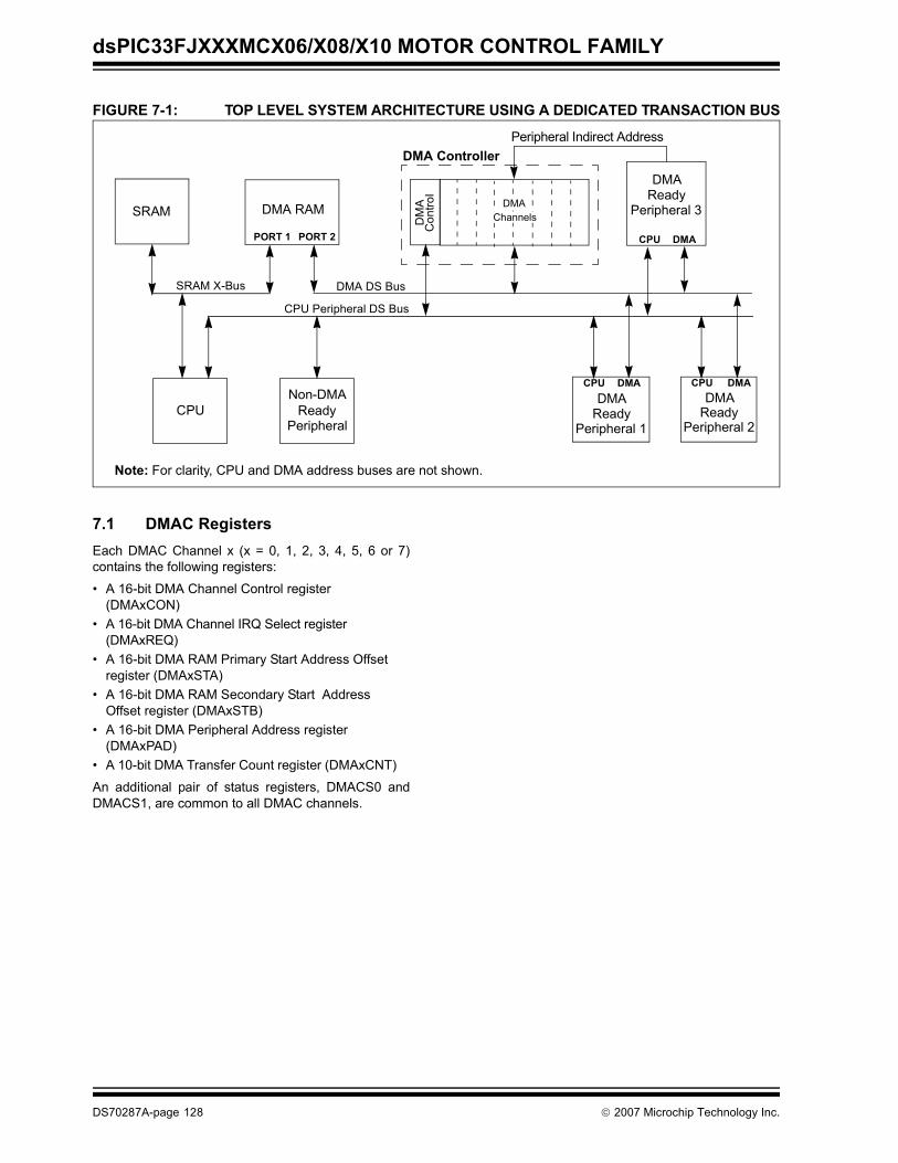
dsPIC33FJXXXMCX06/X08/X10 MOTOR CONTROL FAMILY
FIGURE 7-1: TOP LEVEL SYSTEM ARCHITECTURE USING A DEDICATED TRANSACTION BUS
7.1 DMAC RegistersEach DMAC Channel x (x = 0, 1, 2, 3, 4, 5, 6 or 7)contains the following registers:
• A 16-bit DMA Channel Control register (DMAxCON)
• A 16-bit DMA Channel IRQ Select register (DMAxREQ)
• A 16-bit DMA RAM Primary Start Address Offset register (DMAxSTA)
• A 16-bit DMA RAM Secondary Start Address Offset register (DMAxSTB)
• A 16-bit DMA Peripheral Address register (DMAxPAD)
• A 10-bit DMA Transfer Count register (DMAxCNT)
An additional pair of status registers, DMACS0 andDMACS1, are common to all DMAC channels.
CPU
SRAM DMA RAM
CPU Peripheral DS Bus
Peripheral 3
DMA
Peripheral
Non-DMA
SRAM X-Bus
PORT 2PORT 1
Peripheral 1
DMAReady
Peripheral 2
DMAReadyReady
Ready
DMA DS Bus
CPU DMA
CPU DMA CPU DMA
Peripheral Indirect Address
Note: For clarity, CPU and DMA address buses are not shown.
DM
AC
ontro
l
DMA Controller
DMAChannels
DS70287A-page 128 © 2007 Microchip Technology Inc.
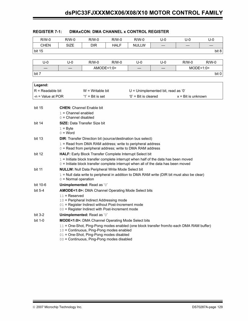
dsPIC33FJXXXMCX06/X08/X10 MOTOR CONTROL FAMILY
REGISTER 7-1: DMAxCON: DMA CHANNEL x CONTROL REGISTER
R/W-0 R/W-0 R/W-0 R/W-0 R/W-0 U-0 U-0 U-0CHEN SIZE DIR HALF NULLW — — —
bit 15 bit 8
U-0 U-0 R/W-0 R/W-0 U-0 U-0 R/W-0 R/W-0— — AMODE<1:0> — — MODE<1:0>
bit 7 bit 0
Legend:R = Readable bit W = Writable bit U = Unimplemented bit, read as ‘0’-n = Value at POR ‘1’ = Bit is set ‘0’ = Bit is cleared x = Bit is unknown
bit 15 CHEN: Channel Enable bit1 = Channel enabled0 = Channel disabled
bit 14 SIZE: Data Transfer Size bit1 = Byte0 = Word
bit 13 DIR: Transfer Direction bit (source/destination bus select)1 = Read from DMA RAM address; write to peripheral address0 = Read from peripheral address; write to DMA RAM address
bit 12 HALF: Early Block Transfer Complete Interrupt Select bit1 = Initiate block transfer complete interrupt when half of the data has been moved0 = Initiate block transfer complete interrupt when all of the data has been moved
bit 11 NULLW: Null Data Peripheral Write Mode Select bit1 = Null data write to peripheral in addition to DMA RAM write (DIR bit must also be clear) 0 = Normal operation
bit 10-6 Unimplemented: Read as ‘0’bit 5-4 AMODE<1:0>: DMA Channel Operating Mode Select bits
11 = Reserved10 = Peripheral Indirect Addressing mode01 = Register Indirect without Post-Increment mode00 = Register Indirect with Post-Increment mode
bit 3-2 Unimplemented: Read as ‘0’bit 1-0 MODE<1:0>: DMA Channel Operating Mode Select bits
11 = One-Shot, Ping-Pong modes enabled (one block transfer from/to each DMA RAM buffer)10 = Continuous, Ping-Pong modes enabled01 = One-Shot, Ping-Pong modes disabled00 = Continuous, Ping-Pong modes disabled
© 2007 Microchip Technology Inc. DS70287A-page 129

dsPIC33FJXXXMCX06/X08/X10 MOTOR CONTROL FAMILY
REGISTER 7-2: DMAxREQ: DMA CHANNEL x IRQ SELECT REGISTER
R/W-0 U-0 U-0 U-0 U-0 U-0 U-0 U-0FORCE(1) — — — — — — —
bit 15 bit 8
U-0 R/W-0 R/W-0 R/W-0 U-0 U-0 R/W-0 R/W-0— IRQSEL6(2) IRQSEL5(2) IRQSEL4(2) IRQSEL3(2) IRQSEL2(2) IRQSEL1(2) IRQSEL0(2)
bit 7 bit 0
Legend:R = Readable bit W = Writable bit U = Unimplemented bit, read as ‘0’-n = Value at POR ‘1’ = Bit is set ‘0’ = Bit is cleared x = Bit is unknown
bit 15 FORCE: Force DMA Transfer bit(1)
1 = Force a single DMA transfer (Manual mode)0 = Automatic DMA transfer initiation by DMA request
bit 14-7 Unimplemented: Read as ‘0’bit 6-0 IRQSEL<6:0>: DMA Peripheral IRQ Number Select bits(2)
0000000-1111111 = DMAIRQ0-DMAIRQ127 selected to be Channel DMAREQNote 1: The FORCE bit cannot be cleared by the user. The FORCE bit is cleared by hardware when the forced
DMA transfer is complete.2: Please see Table 6-1 for a complete listing of IRQ numbers for all interrupt sources.
DS70287A-page 130 © 2007 Microchip Technology Inc.
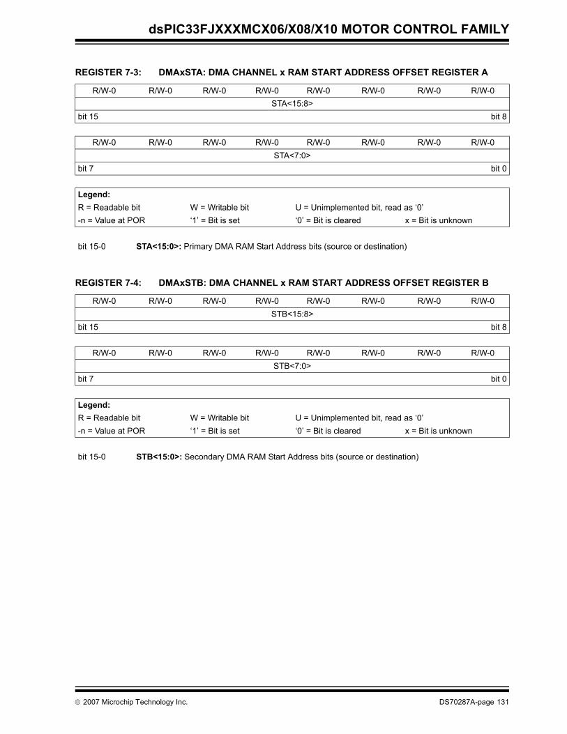
dsPIC33FJXXXMCX06/X08/X10 MOTOR CONTROL FAMILY
REGISTER 7-3: DMAxSTA: DMA CHANNEL x RAM START ADDRESS OFFSET REGISTER A
R/W-0 R/W-0 R/W-0 R/W-0 R/W-0 R/W-0 R/W-0 R/W-0STA<15:8>
bit 15 bit 8
R/W-0 R/W-0 R/W-0 R/W-0 R/W-0 R/W-0 R/W-0 R/W-0STA<7:0>
bit 7 bit 0
Legend:R = Readable bit W = Writable bit U = Unimplemented bit, read as ‘0’-n = Value at POR ‘1’ = Bit is set ‘0’ = Bit is cleared x = Bit is unknown
bit 15-0 STA<15:0>: Primary DMA RAM Start Address bits (source or destination)
REGISTER 7-4: DMAxSTB: DMA CHANNEL x RAM START ADDRESS OFFSET REGISTER B
R/W-0 R/W-0 R/W-0 R/W-0 R/W-0 R/W-0 R/W-0 R/W-0STB<15:8>
bit 15 bit 8
R/W-0 R/W-0 R/W-0 R/W-0 R/W-0 R/W-0 R/W-0 R/W-0STB<7:0>
bit 7 bit 0
Legend:R = Readable bit W = Writable bit U = Unimplemented bit, read as ‘0’-n = Value at POR ‘1’ = Bit is set ‘0’ = Bit is cleared x = Bit is unknown
bit 15-0 STB<15:0>: Secondary DMA RAM Start Address bits (source or destination)
© 2007 Microchip Technology Inc. DS70287A-page 131
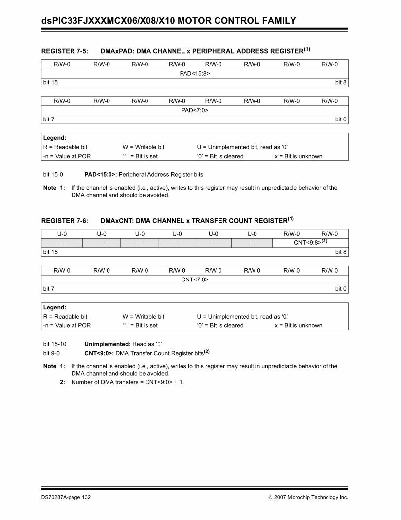
dsPIC33FJXXXMCX06/X08/X10 MOTOR CONTROL FAMILY
REGISTER 7-5: DMAxPAD: DMA CHANNEL x PERIPHERAL ADDRESS REGISTER(1)
R/W-0 R/W-0 R/W-0 R/W-0 R/W-0 R/W-0 R/W-0 R/W-0PAD<15:8>
bit 15 bit 8
R/W-0 R/W-0 R/W-0 R/W-0 R/W-0 R/W-0 R/W-0 R/W-0PAD<7:0>
bit 7 bit 0
Legend:R = Readable bit W = Writable bit U = Unimplemented bit, read as ‘0’-n = Value at POR ‘1’ = Bit is set ‘0’ = Bit is cleared x = Bit is unknown
bit 15-0 PAD<15:0>: Peripheral Address Register bits
Note 1: If the channel is enabled (i.e., active), writes to this register may result in unpredictable behavior of the DMA channel and should be avoided.
REGISTER 7-6: DMAxCNT: DMA CHANNEL x TRANSFER COUNT REGISTER(1)
U-0 U-0 U-0 U-0 U-0 U-0 R/W-0 R/W-0— — — — — — CNT<9:8>(2)
bit 15 bit 8
R/W-0 R/W-0 R/W-0 R/W-0 R/W-0 R/W-0 R/W-0 R/W-0CNT<7:0>
bit 7 bit 0
Legend:R = Readable bit W = Writable bit U = Unimplemented bit, read as ‘0’-n = Value at POR ‘1’ = Bit is set ‘0’ = Bit is cleared x = Bit is unknown
bit 15-10 Unimplemented: Read as ‘0’bit 9-0 CNT<9:0>: DMA Transfer Count Register bits(2)
Note 1: If the channel is enabled (i.e., active), writes to this register may result in unpredictable behavior of the DMA channel and should be avoided.
2: Number of DMA transfers = CNT<9:0> + 1.
DS70287A-page 132 © 2007 Microchip Technology Inc.
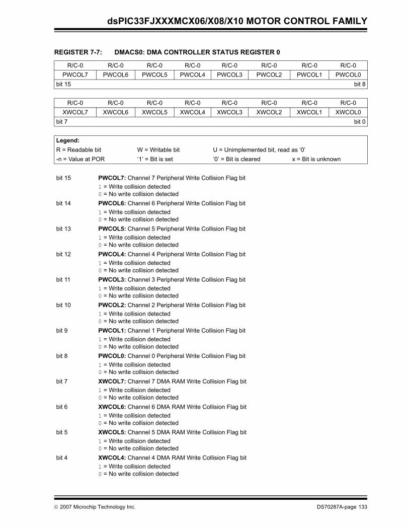
dsPIC33FJXXXMCX06/X08/X10 MOTOR CONTROL FAMILY
REGISTER 7-7: DMACS0: DMA CONTROLLER STATUS REGISTER 0
R/C-0 R/C-0 R/C-0 R/C-0 R/C-0 R/C-0 R/C-0 R/C-0PWCOL7 PWCOL6 PWCOL5 PWCOL4 PWCOL3 PWCOL2 PWCOL1 PWCOL0
bit 15 bit 8
R/C-0 R/C-0 R/C-0 R/C-0 R/C-0 R/C-0 R/C-0 R/C-0XWCOL7 XWCOL6 XWCOL5 XWCOL4 XWCOL3 XWCOL2 XWCOL1 XWCOL0
bit 7 bit 0
Legend:R = Readable bit W = Writable bit U = Unimplemented bit, read as ‘0’-n = Value at POR ‘1’ = Bit is set ‘0’ = Bit is cleared x = Bit is unknown
bit 15 PWCOL7: Channel 7 Peripheral Write Collision Flag bit1 = Write collision detected0 = No write collision detected
bit 14 PWCOL6: Channel 6 Peripheral Write Collision Flag bit1 = Write collision detected0 = No write collision detected
bit 13 PWCOL5: Channel 5 Peripheral Write Collision Flag bit1 = Write collision detected0 = No write collision detected
bit 12 PWCOL4: Channel 4 Peripheral Write Collision Flag bit1 = Write collision detected0 = No write collision detected
bit 11 PWCOL3: Channel 3 Peripheral Write Collision Flag bit1 = Write collision detected0 = No write collision detected
bit 10 PWCOL2: Channel 2 Peripheral Write Collision Flag bit1 = Write collision detected0 = No write collision detected
bit 9 PWCOL1: Channel 1 Peripheral Write Collision Flag bit1 = Write collision detected0 = No write collision detected
bit 8 PWCOL0: Channel 0 Peripheral Write Collision Flag bit1 = Write collision detected0 = No write collision detected
bit 7 XWCOL7: Channel 7 DMA RAM Write Collision Flag bit1 = Write collision detected0 = No write collision detected
bit 6 XWCOL6: Channel 6 DMA RAM Write Collision Flag bit1 = Write collision detected0 = No write collision detected
bit 5 XWCOL5: Channel 5 DMA RAM Write Collision Flag bit1 = Write collision detected0 = No write collision detected
bit 4 XWCOL4: Channel 4 DMA RAM Write Collision Flag bit1 = Write collision detected0 = No write collision detected
© 2007 Microchip Technology Inc. DS70287A-page 133
dsPIC33FJXXXMCX06/X08/X10 MOTOR CONTROL FAMILY
bit 3 XWCOL3: Channel 3 DMA RAM Write Collision Flag bit1 = Write collision detected0 = No write collision detected
bit 2 XWCOL2: Channel 2 DMA RAM Write Collision Flag bit1 = Write collision detected0 = No write collision detected
bit 1 XWCOL1: Channel 1 DMA RAM Write Collision Flag bit1 = Write collision detected0 = No write collision detected
bit 0 XWCOL0: Channel 0 DMA RAM Write Collision Flag bit1 = Write collision detected0 = No write collision detected
REGISTER 7-7: DMACS0: DMA CONTROLLER STATUS REGISTER 0 (CONTINUED)
DS70287A-page 134 © 2007 Microchip Technology Inc.
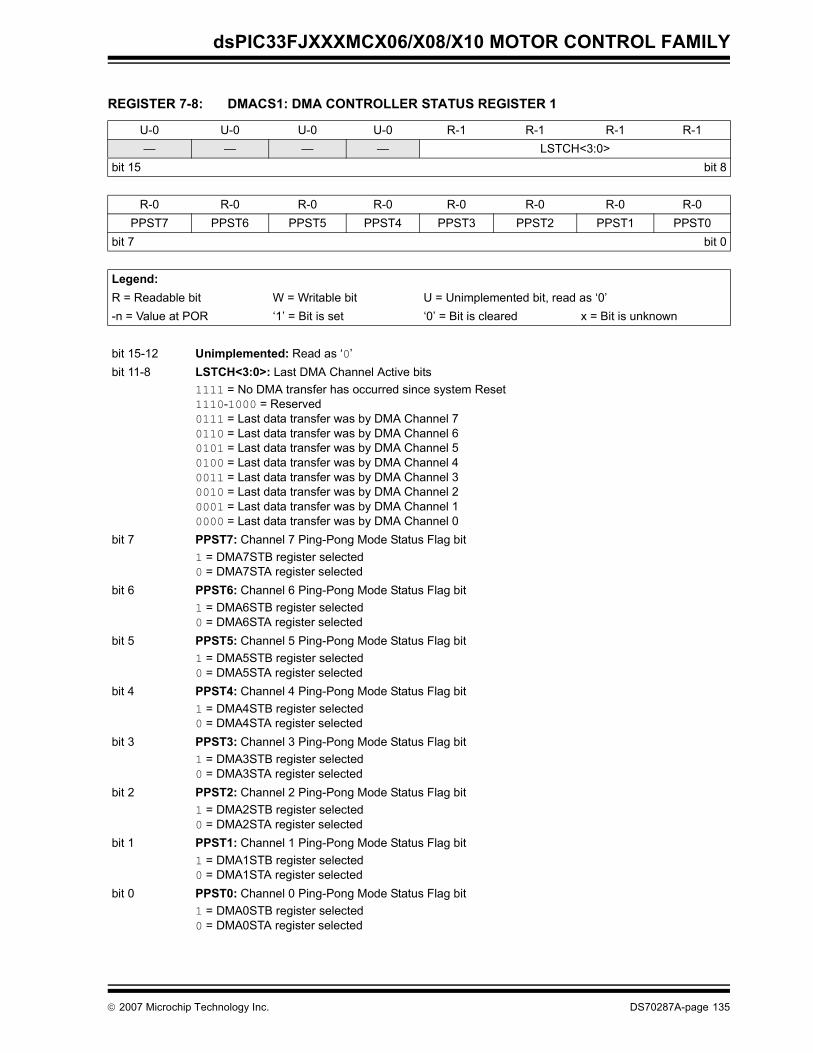
dsPIC33FJXXXMCX06/X08/X10 MOTOR CONTROL FAMILY
REGISTER 7-8: DMACS1: DMA CONTROLLER STATUS REGISTER 1
U-0 U-0 U-0 U-0 R-1 R-1 R-1 R-1— — — — LSTCH<3:0>
bit 15 bit 8
R-0 R-0 R-0 R-0 R-0 R-0 R-0 R-0PPST7 PPST6 PPST5 PPST4 PPST3 PPST2 PPST1 PPST0
bit 7 bit 0
Legend:R = Readable bit W = Writable bit U = Unimplemented bit, read as ‘0’-n = Value at POR ‘1’ = Bit is set ‘0’ = Bit is cleared x = Bit is unknown
bit 15-12 Unimplemented: Read as ‘0’bit 11-8 LSTCH<3:0>: Last DMA Channel Active bits
1111 = No DMA transfer has occurred since system Reset1110-1000 = Reserved0111 = Last data transfer was by DMA Channel 70110 = Last data transfer was by DMA Channel 60101 = Last data transfer was by DMA Channel 50100 = Last data transfer was by DMA Channel 40011 = Last data transfer was by DMA Channel 30010 = Last data transfer was by DMA Channel 20001 = Last data transfer was by DMA Channel 10000 = Last data transfer was by DMA Channel 0
bit 7 PPST7: Channel 7 Ping-Pong Mode Status Flag bit1 = DMA7STB register selected0 = DMA7STA register selected
bit 6 PPST6: Channel 6 Ping-Pong Mode Status Flag bit1 = DMA6STB register selected0 = DMA6STA register selected
bit 5 PPST5: Channel 5 Ping-Pong Mode Status Flag bit1 = DMA5STB register selected0 = DMA5STA register selected
bit 4 PPST4: Channel 4 Ping-Pong Mode Status Flag bit1 = DMA4STB register selected0 = DMA4STA register selected
bit 3 PPST3: Channel 3 Ping-Pong Mode Status Flag bit1 = DMA3STB register selected0 = DMA3STA register selected
bit 2 PPST2: Channel 2 Ping-Pong Mode Status Flag bit1 = DMA2STB register selected0 = DMA2STA register selected
bit 1 PPST1: Channel 1 Ping-Pong Mode Status Flag bit1 = DMA1STB register selected0 = DMA1STA register selected
bit 0 PPST0: Channel 0 Ping-Pong Mode Status Flag bit1 = DMA0STB register selected0 = DMA0STA register selected
© 2007 Microchip Technology Inc. DS70287A-page 135
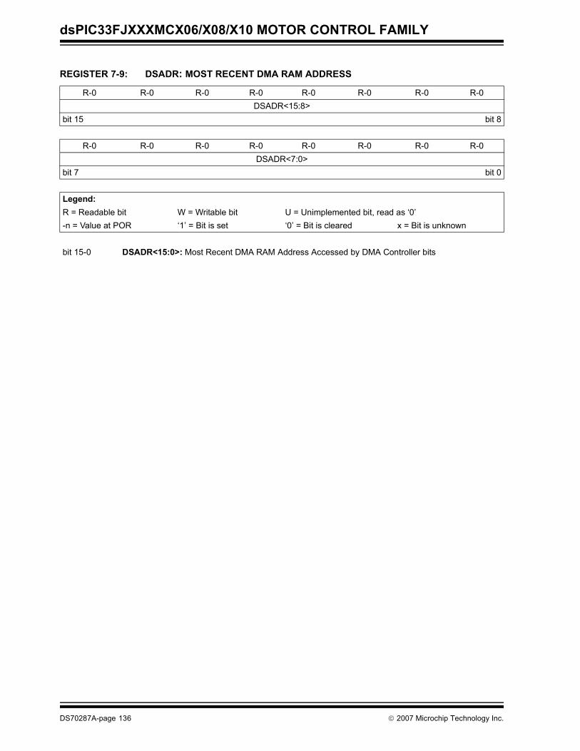
dsPIC33FJXXXMCX06/X08/X10 MOTOR CONTROL FAMILY
REGISTER 7-9: DSADR: MOST RECENT DMA RAM ADDRESS
R-0 R-0 R-0 R-0 R-0 R-0 R-0 R-0DSADR<15:8>
bit 15 bit 8
R-0 R-0 R-0 R-0 R-0 R-0 R-0 R-0DSADR<7:0>
bit 7 bit 0
Legend:R = Readable bit W = Writable bit U = Unimplemented bit, read as ‘0’-n = Value at POR ‘1’ = Bit is set ‘0’ = Bit is cleared x = Bit is unknown
bit 15-0 DSADR<15:0>: Most Recent DMA RAM Address Accessed by DMA Controller bits
DS70287A-page 136 © 2007 Microchip Technology Inc.
dsPIC33FJXXXMCX06/X08/X10 MOTOR CONTROL FAMILY
8.0 OSCILLATOR CONFIGURATION
The dsPIC33FJXXXMCX06/X08/X10 Motor ControlFamily oscillator system provides the following:
• Various external and internal oscillator options as
clock sources• An on-chip PLL to scale the internal operating
frequency to the required system clock frequency• The internal FRC oscillator can also be used with
the PLL, thereby allowing full-speed operation without any external clock generation hardware
• Clock switching between various clock sources• Programmable clock postscaler for system power
savings• A Fail-Safe Clock Monitor (FSCM) that detects
clock failure and takes fail-safe measures• A Clock Control register (OSCCON)• Nonvolatile Configuration bits for main oscillator
selection
A simplified diagram of the oscillator system is shownin Figure 8-1.
FIGURE 8-1: dsPIC33FJXXXMCX06/X08/X10 MOTOR CONTROL FAMILY OSCILLATOR SYSTEM DIAGRAM
Note: This data sheet summarizes the featuresof this group of dsPIC33FJXXXMCX06/X08/X10 Motor Control Family devices. Itis not intended to be a comprehensivereference source. To complement theinformation in this data sheet, refer to the“dsPIC33F Family Reference Manual”.Refer to the Microchip web site(www.microchip.com) for the latestdsPIC33F family reference manualchapters.
dsPIC33F
Secondary Oscillator
LPOSCEN
SOSCO
SOSCI
Timer 1
OSC1
OSC2
Primary Oscillator
XTPLL, HSPLL,
XT, HS, EC
FRCDIV<2:0>
WDT, PWRT, FSCM
FRCDIVN
SOSC
FRCDIV16
ECPLL, FRCPLL
NOSC<2:0> FNOSC<2:0>
Reset
FRCOscillator
LPRCOscillator
DOZE<2:0>
S3
S1
S2
S1/S3
S7
S6
FRC
LPRC
S0
S5
S4
÷ 16
Clock Switch
S7
Clock Fail
÷ 2
TUN<5:0>
PLL(1) FCY
FOSC
FRC
DIV
DO
ZE
Note 1: See Figure 8-2 for PLL details
© 2007 Microchip Technology Inc. DS70287A-page 137
dsPIC33FJXXXMCX06/X08/X10 MOTOR CONTROL FAMILY
8.1 CPU Clocking SystemThere are seven system clock options provided by thedsPIC33FJXXXMCX06/X08/X10 Motor Control Family:
• FRC Oscillator• FRC Oscillator with PLL• Primary (XT, HS or EC) Oscillator• Primary Oscillator with PLL• Secondary (LP) Oscillator • LPRC Oscillator• FRC Oscillator with postscaler
8.1.1 SYSTEM CLOCK SOURCESThe FRC (Fast RC) internal oscillator runs at a nominalfrequency of 7.37 MHz. The user software can tune theFRC frequency. User software can optionally specify afactor (ranging from 1:2 to 1:256) by which the FRCclock frequency is divided. This factor is selected usingthe FRCDIV<2:0> (CLKDIV<10:8>) bits.
The primary oscillator can use one of the following asits clock source:
1. XT (Crystal): Crystals and ceramic resonators inthe range of 3 MHz to 10 MHz. The crystal isconnected to the OSC1 and OSC2 pins.
2. HS (High-Speed Crystal): Crystals in the rangeof 10 MHz to 40 MHz. The crystal is connectedto the OSC1 and OSC2 pins.
3. EC (External Clock): External clock signal in therange of 0.8 MHz to 64 MHz. The external clocksignal is directly applied to the OSC1 pin.
The secondary (LP) oscillator is designed for low powerand uses a 32.768 kHz crystal or ceramic resonator.The LP oscillator uses the SOSCI and SOSCO pins.
The LPRC (Low-Power RC) internal oscIllator runs at anominal frequency of 32.768 kHz. It is also used as areference clock by the Watchdog Timer (WDT) andFail-Safe Clock Monitor (FSCM).
The clock signals generated by the FRC and primaryoscillators can be optionally applied to an on-chipPhase Locked Loop (PLL) to provide a wide range ofoutput frequencies for device operation. PLLconfiguration is described in Section 8.1.3 “PLLConfiguration”.
8.1.2 SYSTEM CLOCK SELECTIONThe oscillator source that is used at a device Power-onReset event is selected using Configuration bit settings.The oscillator Configuration bit settings are located in theConfiguration registers in the program memory. (Refer toSection 22.1 “Configuration Bits” for further details.)The Initial Oscillator Selection Configuration bits,FNOSC<2:0> (FOSCSEL<2:0>), and the PrimaryOscillator Mode Select Configuration bits,POSCMD<1:0> (FOSC<1:0>), select the oscillatorsource that is used at a Power-on Reset. The FRC pri-mary oscillator is the default (unprogrammed) selection.
The Configuration bits allow users to choose betweentwelve different clock modes, shown in Table 8-1.
The output of the oscillator (or the output of the PLL ifa PLL mode has been selected), FOSC, is divided by 2to generate the device instruction clock (FCY). FCYdefines the operating speed of the device, and speedsup to 40 MHz are supported by thedsPIC33FJXXXMCX06/X08/X10 Motor Control Familyarchitecture.
Instruction execution speed or device operatingfrequency, FCY, is given by the following equation:
EQUATION 8-1: DEVICE OPERATING FREQUENCY
8.1.3 PLL CONFIGURATIONThe primary oscillator and internal FRC oscillator canoptionally use an on-chip PLL to obtain higher speedsof operation. The PLL provides a significant amount offlexibility in selecting the device operating speed. Ablock diagram of the PLL is shown in Figure 8-2.
The output of the primary oscillator or FRC, denoted as‘FIN’, is divided down by a prescale factor (N1) of 2, 3,... or 33 before being provided to the PLL’s VoltageControlled Oscillator (VCO). The input to the VCO mustbe selected to be in the range of 0.8 MHz to 8 MHz.Since the minimum prescale factor is 2, this implies thatFIN must be chosen to be in the range of 1.6 MHz to 16MHz. The prescale factor, ‘N1’, is selected using thePLLPRE<4:0> bits (CLKDIV<4:0>).
The PLL Feedback Divisor, selected using the PLLDIV<8:0> bits (PLLFBD<8:0>), provides a factor, ‘M’,by which the input to the VCO is multiplied. This factormust be selected such that the resulting VCO output frequency is in the range of 100 MHz to 200 MHz.
The VCO output is further divided by a postscale factor,‘N2’. This factor is selected using the PLLPOST<1:0>bits (CLKDIV<7:6>). ‘N2’ can be either 2, 4 or 8, andmust be selected such that the PLL output frequency(FOSC) is in the range of 12.5 MHz to 80 MHz, whichgenerates device operating speeds of 6.25-40 MIPS.
For a primary oscillator or FRC oscillator output, ‘FIN’,the PLL output, ‘FOSC’, is given by the followingequation:
EQUATION 8-2: FOSC CALCULATION
FCY = FOSC/2
( ) M N1 * N2FOSC = FIN *
DS70287A-page 138 © 2007 Microchip Technology Inc.
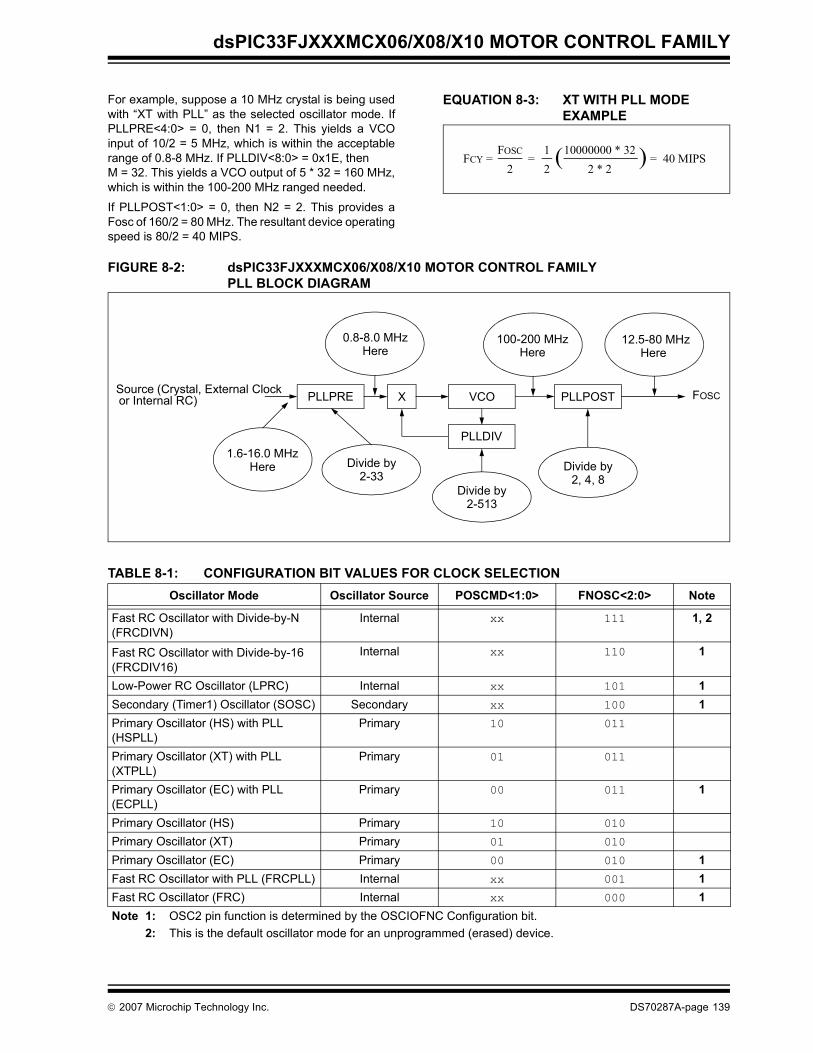
dsPIC33FJXXXMCX06/X08/X10 MOTOR CONTROL FAMILY
For example, suppose a 10 MHz crystal is being usedwith “XT with PLL” as the selected oscillator mode. IfPLLPRE<4:0> = 0, then N1 = 2. This yields a VCOinput of 10/2 = 5 MHz, which is within the acceptablerange of 0.8-8 MHz. If PLLDIV<8:0> = 0x1E, then M = 32. This yields a VCO output of 5 * 32 = 160 MHz,which is within the 100-200 MHz ranged needed.
If PLLPOST<1:0> = 0, then N2 = 2. This provides aFosc of 160/2 = 80 MHz. The resultant device operatingspeed is 80/2 = 40 MIPS.
EQUATION 8-3: XT WITH PLL MODE EXAMPLE
FIGURE 8-2: dsPIC33FJXXXMCX06/X08/X10 MOTOR CONTROL FAMILY PLL BLOCK DIAGRAM
TABLE 8-1: CONFIGURATION BIT VALUES FOR CLOCK SELECTION
FCY = FOSC
2= =
12(10000000 * 32
2 * 2) 40 MIPS
Oscillator Mode Oscillator Source POSCMD<1:0> FNOSC<2:0> Note
Fast RC Oscillator with Divide-by-N (FRCDIVN)
Internal xx 111 1, 2
Fast RC Oscillator with Divide-by-16 (FRCDIV16)
Internal xx 110 1
Low-Power RC Oscillator (LPRC) Internal xx 101 1Secondary (Timer1) Oscillator (SOSC) Secondary xx 100 1Primary Oscillator (HS) with PLL (HSPLL)
Primary 10 011
Primary Oscillator (XT) with PLL (XTPLL)
Primary 01 011
Primary Oscillator (EC) with PLL (ECPLL)
Primary 00 011 1
Primary Oscillator (HS) Primary 10 010
Primary Oscillator (XT) Primary 01 010
Primary Oscillator (EC) Primary 00 010 1Fast RC Oscillator with PLL (FRCPLL) Internal xx 001 1Fast RC Oscillator (FRC) Internal xx 000 1Note 1: OSC2 pin function is determined by the OSCIOFNC Configuration bit.
2: This is the default oscillator mode for an unprogrammed (erased) device.
0.8-8.0 MHzHere
100-200 MHzHere
Divide by2, 4, 8
Divide by2-513
Divide by2-33
1.6-16.0 MHz
Source (Crystal, External Clock PLLPRE X VCO
PLLDIV
PLLPOSTor Internal RC)
Here
12.5-80 MHzHere
FOSC
© 2007 Microchip Technology Inc. DS70287A-page 139
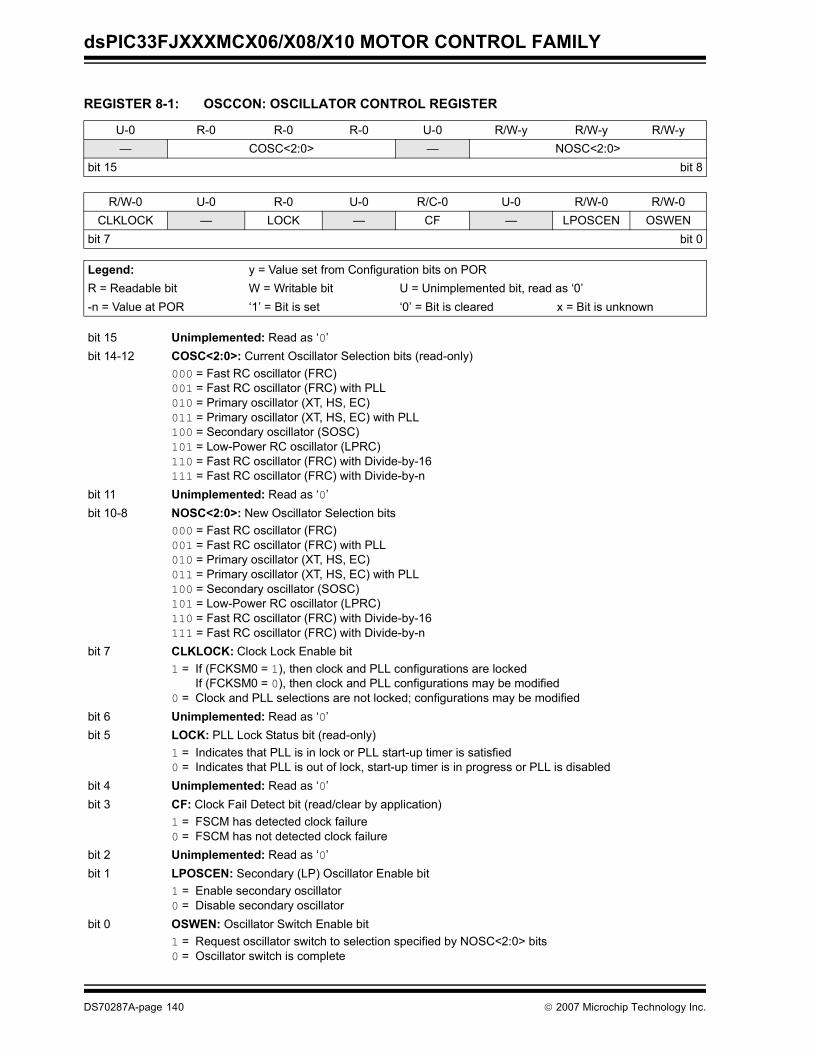
dsPIC33FJXXXMCX06/X08/X10 MOTOR CONTROL FAMILY
REGISTER 8-1: OSCCON: OSCILLATOR CONTROL REGISTER
U-0 R-0 R-0 R-0 U-0 R/W-y R/W-y R/W-y— COSC<2:0> — NOSC<2:0>
bit 15 bit 8
R/W-0 U-0 R-0 U-0 R/C-0 U-0 R/W-0 R/W-0CLKLOCK — LOCK — CF — LPOSCEN OSWEN
bit 7 bit 0
Legend: y = Value set from Configuration bits on PORR = Readable bit W = Writable bit U = Unimplemented bit, read as ‘0’-n = Value at POR ‘1’ = Bit is set ‘0’ = Bit is cleared x = Bit is unknown
bit 15 Unimplemented: Read as ‘0’bit 14-12 COSC<2:0>: Current Oscillator Selection bits (read-only)
000 = Fast RC oscillator (FRC)001 = Fast RC oscillator (FRC) with PLL 010 = Primary oscillator (XT, HS, EC)011 = Primary oscillator (XT, HS, EC) with PLL 100 = Secondary oscillator (SOSC)101 = Low-Power RC oscillator (LPRC)110 = Fast RC oscillator (FRC) with Divide-by-16111 = Fast RC oscillator (FRC) with Divide-by-n
bit 11 Unimplemented: Read as ‘0’bit 10-8 NOSC<2:0>: New Oscillator Selection bits
000 = Fast RC oscillator (FRC)001 = Fast RC oscillator (FRC) with PLL 010 = Primary oscillator (XT, HS, EC)011 = Primary oscillator (XT, HS, EC) with PLL 100 = Secondary oscillator (SOSC)101 = Low-Power RC oscillator (LPRC)110 = Fast RC oscillator (FRC) with Divide-by-16111 = Fast RC oscillator (FRC) with Divide-by-n
bit 7 CLKLOCK: Clock Lock Enable bit 1 = If (FCKSM0 = 1), then clock and PLL configurations are locked
If (FCKSM0 = 0), then clock and PLL configurations may be modified0 = Clock and PLL selections are not locked; configurations may be modified
bit 6 Unimplemented: Read as ‘0’bit 5 LOCK: PLL Lock Status bit (read-only)
1 = Indicates that PLL is in lock or PLL start-up timer is satisfied0 = Indicates that PLL is out of lock, start-up timer is in progress or PLL is disabled
bit 4 Unimplemented: Read as ‘0’bit 3 CF: Clock Fail Detect bit (read/clear by application)
1 = FSCM has detected clock failure0 = FSCM has not detected clock failure
bit 2 Unimplemented: Read as ‘0’bit 1 LPOSCEN: Secondary (LP) Oscillator Enable bit
1 = Enable secondary oscillator0 = Disable secondary oscillator
bit 0 OSWEN: Oscillator Switch Enable bit1 = Request oscillator switch to selection specified by NOSC<2:0> bits0 = Oscillator switch is complete
DS70287A-page 140 © 2007 Microchip Technology Inc.
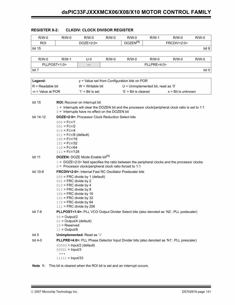
dsPIC33FJXXXMCX06/X08/X10 MOTOR CONTROL FAMILY
REGISTER 8-2: CLKDIV: CLOCK DIVISOR REGISTER
R/W-0 R/W-0 R/W-0 R/W-0 R/W-0 R/W-1 R/W-0 R/W-0ROI DOZE<2:0> DOZEN(1) FRCDIV<2:0>
bit 15 bit 8
R/W-0 R/W-1 U-0 R/W-0 R/W-0 R/W-0 R/W-0 R/W-0PLLPOST<1:0> — PLLPRE<4:0>
bit 7 bit 0
Legend: y = Value set from Configuration bits on PORR = Readable bit W = Writable bit U = Unimplemented bit, read as ‘0’-n = Value at POR ‘1’ = Bit is set ‘0’ = Bit is cleared x = Bit is unknown
bit 15 ROI: Recover on Interrupt bit1 = Interrupts will clear the DOZEN bit and the processor clock/peripheral clock ratio is set to 1:10 = Interrupts have no effect on the DOZEN bit
bit 14-12 DOZE<2:0>: Processor Clock Reduction Select bits000 = FCY/1001 = FCY/2010 = FCY/4011 = FCY/8 (default)100 = FCY/16101 = FCY/32110 = FCY/64111 = FCY/128
bit 11 DOZEN: DOZE Mode Enable bit(1)
1 = DOZE<2:0> field specifies the ratio between the peripheral clocks and the processor clocks0 = Processor clock/peripheral clock ratio forced to 1:1
bit 10-8 FRCDIV<2:0>: Internal Fast RC Oscillator Postscaler bits000 = FRC divide by 1 (default)001 = FRC divide by 2010 = FRC divide by 4011 = FRC divide by 8100 = FRC divide by 16101 = FRC divide by 32110 = FRC divide by 64111 = FRC divide by 256
bit 7-6 PLLPOST<1:0>: PLL VCO Output Divider Select bits (also denoted as ‘N2’, PLL postscaler)00 = Output/2 01 = Output/4 (default)10 = Reserved11 = Output/8
bit 5 Unimplemented: Read as ‘0’bit 4-0 PLLPRE<4:0>: PLL Phase Detector Input Divider bits (also denoted as ‘N1’, PLL prescaler)
00000 = Input/2 (default)00001 = Input/3 • • • 11111 = Input/33
Note 1: This bit is cleared when the ROI bit is set and an interrupt occurs.
© 2007 Microchip Technology Inc. DS70287A-page 141
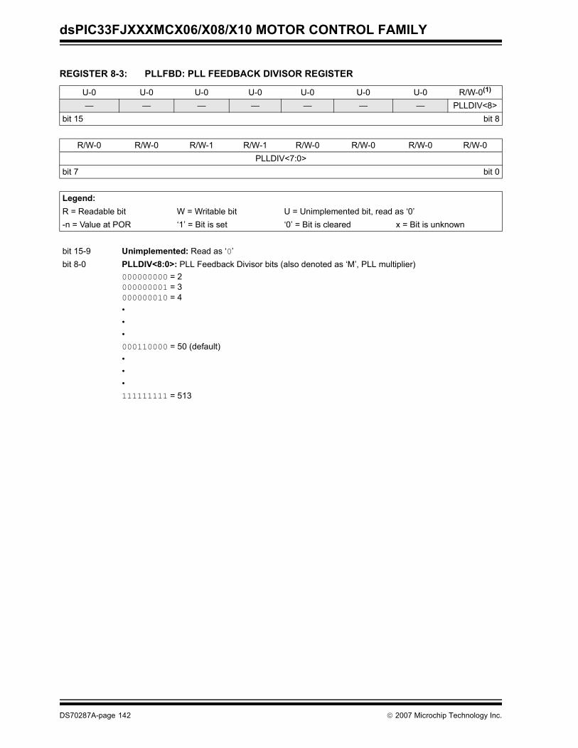
dsPIC33FJXXXMCX06/X08/X10 MOTOR CONTROL FAMILY
REGISTER 8-3: PLLFBD: PLL FEEDBACK DIVISOR REGISTER
U-0 U-0 U-0 U-0 U-0 U-0 U-0 R/W-0(1)
— — — — — — — PLLDIV<8>bit 15 bit 8
R/W-0 R/W-0 R/W-1 R/W-1 R/W-0 R/W-0 R/W-0 R/W-0PLLDIV<7:0>
bit 7 bit 0
Legend:R = Readable bit W = Writable bit U = Unimplemented bit, read as ‘0’-n = Value at POR ‘1’ = Bit is set ‘0’ = Bit is cleared x = Bit is unknown
bit 15-9 Unimplemented: Read as ‘0’bit 8-0 PLLDIV<8:0>: PLL Feedback Divisor bits (also denoted as ‘M’, PLL multiplier)
000000000 = 2000000001 = 3000000010 = 4•••000110000 = 50 (default)•••111111111 = 513
DS70287A-page 142 © 2007 Microchip Technology Inc.
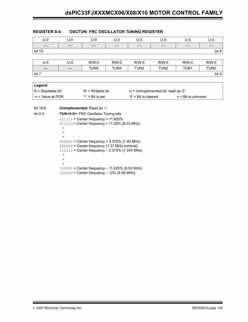
dsPIC33FJXXXMCX06/X08/X10 MOTOR CONTROL FAMILY
REGISTER 8-4: OSCTUN: FRC OSCILLATOR TUNING REGISTER
U-0 U-0 U-0 U-0 U-0 U-0 U-0 U-0— — — — — — — —
bit 15 bit 8
U-0 U-0 R/W-0 R/W-0 R/W-0 R/W-0 R/W-0 R/W-0— — TUN5 TUN4 TUN3 TUN2 TUN1 TUN0
bit 7 bit 0
Legend:R = Readable bit W = Writable bit U = Unimplemented bit, read as ‘0’-n = Value at POR ‘1’ = Bit is set ‘0’ = Bit is cleared x = Bit is unknown
bit 15-6 Unimplemented: Read as ‘0’bit 5-0 TUN<5:0>: FRC Oscillator Tuning bits
011111 = Center frequency + 11.625%011110 = Center frequency + 11.25% (8.23 MHz) • • •000001 = Center frequency + 0.375% (7.40 MHz) 000000 = Center frequency (7.37 MHz nominal)111111 = Center frequency – 0.375% (7.345 MHz) • • •100001 = Center frequency – 11.625% (6.52 MHz) 100000 = Center frequency – 12% (6.49 MHz)
© 2007 Microchip Technology Inc. DS70287A-page 143

dsPIC33FJXXXMCX06/X08/X10 MOTOR CONTROL FAMILY
8.2 Clock Switching OperationApplications are free to switch between any of the fourclock sources (Primary, LP, FRC and LPRC) undersoftware control at any time. To limit the possible sideeffects that could result from this flexibility,dsPIC33FJXXXMCX06/X08/X10 Motor Control Familydevices have a safeguard lock built into the switchprocess.
8.2.1 ENABLING CLOCK SWITCHINGTo enable clock switching, the FCKSM1 Configurationbit in the Configuration register must be programmed to‘0’. (Refer to Section 22.1 “Configuration Bits” forfurther details.) If the FCKSM1 Configuration bit isunprogrammed (‘1’), the clock switching function andFail-Safe Clock Monitor function are disabled. This isthe default setting.
The NOSC control bits (OSCCON<10:8>) do notcontrol the clock selection when clock switching isdisabled. However, the COSC bits (OSCCON<14:12>)reflect the clock source selected by the FNOSCConfiguration bits.
The OSWEN control bit (OSCCON<0>) has no effectwhen clock switching is disabled. It is held at ‘0’ at alltimes.
8.2.2 OSCILLATOR SWITCHING SEQUENCE
At a minimum, performing a clock switch requires thefollowing basic sequence:
1. If desired, read the COSC bits(OSCCON<14:12>) to determine the currentoscillator source.
2. Perform the unlock sequence to allow a write tothe OSCCON register high byte.
3. Write the appropriate value to the NOSC controlbits (OSCCON<10:8>) for the new oscillatorsource.
4. Perform the unlock sequence to allow a write tothe OSCCON register low byte.
5. Set the OSWEN bit to initiate the oscillatorswitch.
Once the basic sequence is completed, the systemclock hardware responds automatically as follows:
1. The clock switching hardware compares theCOSC status bits with the new value of theNOSC control bits. If they are the same, then theclock switch is a redundant operation. In thiscase, the OSWEN bit is cleared automaticallyand the clock switch is aborted.
2. If a valid clock switch has been initiated, theLOCK (OSCCON<5>) and the CF(OSCCON<3>) status bits are cleared.
3. The new oscillator is turned on by the hardwareif it is not currently running. If a crystal oscillatormust be turned on, the hardware waits until theOscillator Start-up Timer (OST) expires. If thenew source is using the PLL, the hardware waitsuntil a PLL lock is detected (LOCK = 1).
4. The hardware waits for 10 clock cycles from thenew clock source and then performs the clockswitch.
5. The hardware clears the OSWEN bit to indicate asuccessful clock transition. In addition, the NOSCbit values are transferred to the COSC status bits.
6. The old clock source is turned off at this time,with the exception of LPRC (if WDT or FSCMare enabled) or LP (if LPOSCEN remains set).
8.3 Fail-Safe Clock Monitor (FSCM)The Fail-Safe Clock Monitor (FSCM) allows the deviceto continue to operate even in the event of an oscillatorfailure. The FSCM function is enabled by programming.If the FSCM function is enabled, the LPRC internaloscillator runs at all times (except during Sleep mode)and is not subject to control by the Watchdog Timer.
In the event of an oscillator failure, the FSCMgenerates a clock failure trap event and switches thesystem clock over to the FRC oscillator. Then theapplication program can either attempt to restart theoscillator or execute a controlled shutdown. The trapcan be treated as a warm Reset by simply loading theReset address into the oscillator fail trap vector.
If the PLL multiplier is used to scale the system clock,the internal FRC is also multiplied by the same factoron clock failure. Essentially, the device switches toFRC with PLL on a clock failure.
Note: Primary Oscillator mode has three differentsubmodes (XT, HS and EC) which aredetermined by the POSCMD<1:0> Config-uration bits. While an application canswitch to and from Primary Oscillatormode in software, it cannot switchbetween the different primary submodeswithout reprogramming the device.
Note 1: The processor continues to execute codethroughout the clock switching sequence.Timing sensitive code should not beexecuted during this time.
2: Direct clock switches between any primaryoscillator mode with PLL and FRCPLLmode are not permitted. This applies toclock switches in either direction. In theseinstances, the application must switch toFRC mode as a transition clock sourcebetween the two PLL modes.
DS70287A-page 144 © 2007 Microchip Technology Inc.
dsPIC33FJXXXMCX06/X08/X10 MOTOR CONTROL FAMILY
9.0 POWER-SAVING FEATURES
The dsPIC33FJXXXMCX06/X08/X10 Motor ControlFamily devices provide the ability to manage powerconsumption by selectively managing clocking to theCPU and the peripherals. In general, a lower clock fre-quency and a reduction in the number of circuits beingclocked constitutes lower consumed power.dsPIC33FJXXXMCX06/X08/X10 Motor Control Familydevices can manage power consumption in four differ-ent ways:
• Clock frequency• Instruction-based Sleep and Idle modes• Software-controlled Doze mode• Selective peripheral control in software
Combinations of these methods can be used to selec-tively tailor an application’s power consumption whilestill maintaining critical application features, such astiming-sensitive communications.
9.1 Clock Frequency and Clock Switching
dsPIC33FJXXXMCX06/X08/X10 Motor Control Familydevices allow a wide range of clock frequencies to beselected under application control. If the system clockconfiguration is not locked, users can chooselow-power or high-precision oscillators by simplychanging the NOSC bits (OSCCON<10:8>). The pro-cess of changing a system clock during operation, aswell as limitations to the process, are discussed inmore detail in Section 8.0 “Oscillator Configura-tion”.
9.2 Instruction-Based Power-Saving Modes
dsPIC33FJXXXMCX06/X08/X10 Motor Control Familydevices have two special power-saving modes that areentered through the execution of a special PWRSAVinstruction. Sleep mode stops clock operation and haltsall code execution. Idle mode halts the CPU and codeexecution, but allows peripheral modules to continueoperation. The assembly syntax of the PWRSAV instruc-tion is shown in Example 9-1.
Sleep and Idle modes can be exited as a result of anenabled interrupt, WDT time-out or a device Reset. Whenthe device exits these modes, it is said to “wake-up”.
9.2.1 SLEEP MODE Sleep mode has the following features:
• The system clock source is shut down. If an on-chip oscillator is used, it is turned off.
• The device current consumption is reduced to a minimum, provided that no I/O pin is sourcing current.
• The Fail-Safe Clock Monitor does not operate during Sleep mode since the system clock source is disabled.
• The LPRC clock continues to run in Sleep mode if the WDT is enabled.
• The WDT, if enabled, is automatically cleared prior to entering Sleep mode.
• Some device features or peripherals may continue to operate in Sleep mode. This includes items such as the input change notification on the I/O ports and peripherals that use an external clock input. Any peripheral that requires the system clock source for its operation is disabled in Sleep mode.
The device will wake-up from Sleep mode on any of thethe following events:
• Any interrupt source that is individually enabled• Any form of device Reset• A WDT time-out
On wake-up from Sleep, the processor restarts with thesame clock source that was active when Sleep modewas entered.
EXAMPLE 9-1: PWRSAV INSTRUCTION SYNTAX
Note: This data sheet summarizes the featuresof this groupof dsPIC33FJXXXMCX06/X08/X10 MotorControl Family devices. It is not intendedto be a comprehensive reference source.To complement the information in this datasheet, refer to the “dsPIC33F FamilyReference Manual”. Refer to theMicrochip web site (www.microchip.com)for the latest dsPIC33F family referencemanual chapters.
Note: SLEEP_MODE and IDLE_MODE areconstants defined in the assemblerinclude file for the selected device.
PWRSAV #SLEEP_MODE ; Put the device into SLEEP modePWRSAV #IDLE_MODE ; Put the device into IDLE mode
© 2007 Microchip Technology Inc. DS70287A-page 145
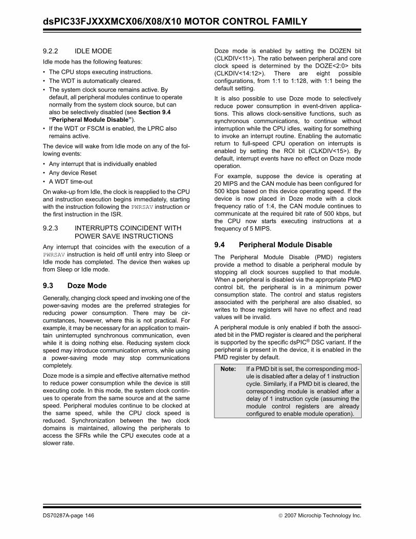
dsPIC33FJXXXMCX06/X08/X10 MOTOR CONTROL FAMILY
9.2.2 IDLE MODE Idle mode has the following features:
• The CPU stops executing instructions.• The WDT is automatically cleared.• The system clock source remains active. By
default, all peripheral modules continue to operate normally from the system clock source, but can also be selectively disabled (see Section 9.4 “Peripheral Module Disable”).
• If the WDT or FSCM is enabled, the LPRC also remains active.
The device will wake from Idle mode on any of the fol-lowing events:
• Any interrupt that is individually enabled• Any device Reset• A WDT time-out
On wake-up from Idle, the clock is reapplied to the CPUand instruction execution begins immediately, startingwith the instruction following the PWRSAV instruction orthe first instruction in the ISR.
9.2.3 INTERRUPTS COINCIDENT WITH POWER SAVE INSTRUCTIONS
Any interrupt that coincides with the execution of aPWRSAV instruction is held off until entry into Sleep orIdle mode has completed. The device then wakes upfrom Sleep or Idle mode.
9.3 Doze ModeGenerally, changing clock speed and invoking one of thepower-saving modes are the preferred strategies forreducing power consumption. There may be cir-cumstances, however, where this is not practical. Forexample, it may be necessary for an application to main-tain uninterrupted synchronous communication, evenwhile it is doing nothing else. Reducing system clockspeed may introduce communication errors, while usinga power-saving mode may stop communicationscompletely.
Doze mode is a simple and effective alternative methodto reduce power consumption while the device is stillexecuting code. In this mode, the system clock contin-ues to operate from the same source and at the samespeed. Peripheral modules continue to be clocked atthe same speed, while the CPU clock speed isreduced. Synchronization between the two clockdomains is maintained, allowing the peripherals toaccess the SFRs while the CPU executes code at aslower rate.
Doze mode is enabled by setting the DOZEN bit(CLKDIV<11>). The ratio between peripheral and coreclock speed is determined by the DOZE<2:0> bits(CLKDIV<14:12>). There are eight possibleconfigurations, from 1:1 to 1:128, with 1:1 being thedefault setting.
It is also possible to use Doze mode to selectivelyreduce power consumption in event-driven applica-tions. This allows clock-sensitive functions, such assynchronous communications, to continue withoutinterruption while the CPU idles, waiting for somethingto invoke an interrupt routine. Enabling the automaticreturn to full-speed CPU operation on interrupts isenabled by setting the ROI bit (CLKDIV<15>). Bydefault, interrupt events have no effect on Doze modeoperation.
For example, suppose the device is operating at20 MIPS and the CAN module has been configured for500 kbps based on this device operating speed. If thedevice is now placed in Doze mode with a clockfrequency ratio of 1:4, the CAN module continues tocommunicate at the required bit rate of 500 kbps, butthe CPU now starts executing instructions at afrequency of 5 MIPS.
9.4 Peripheral Module DisableThe Peripheral Module Disable (PMD) registersprovide a method to disable a peripheral module bystopping all clock sources supplied to that module.When a peripheral is disabled via the appropriate PMDcontrol bit, the peripheral is in a minimum powerconsumption state. The control and status registersassociated with the peripheral are also disabled, sowrites to those registers will have no effect and readvalues will be invalid.
A peripheral module is only enabled if both the associ-ated bit in the PMD register is cleared and the peripheralis supported by the specific dsPIC® DSC variant. If theperipheral is present in the device, it is enabled in thePMD register by default.
Note: If a PMD bit is set, the corresponding mod-ule is disabled after a delay of 1 instructioncycle. Similarly, if a PMD bit is cleared, thecorresponding module is enabled after adelay of 1 instruction cycle (assuming themodule control registers are alreadyconfigured to enable module operation).
DS70287A-page 146 © 2007 Microchip Technology Inc.

dsPIC33FJXXXMCX06/X08/X10 MOTOR CONTROL FAMILY
10.0 I/O PORTS
All of the device pins (except VDD, VSS, MCLR andOSC1/CLKIN) are shared between the peripherals andthe parallel I/O ports. All I/O input ports feature SchmittTrigger inputs for improved noise immunity.
10.1 Parallel I/O (PIO) PortsA parallel I/O port that shares a pin with a peripheral is,in general, subservient to the peripheral. The periph-eral’s output buffer data and control signals areprovided to a pair of multiplexers. The multiplexersselect whether the peripheral or the associated porthas ownership of the output data and control signals ofthe I/O pin. The logic also prevents “loop through,” inwhich a port’s digital output can drive the input of a
peripheral that shares the same pin. Figure 10-1 showshow ports are shared with other peripherals and theassociated I/O pin to which they are connected.
When a peripheral is enabled and actively driving anassociated pin, the use of the pin as a general purposeoutput pin is disabled. The I/O pin may be read, but theoutput driver for the parallel port bit will be disabled. Ifa peripheral is enabled but the peripheral is not activelydriving a pin, that pin may be driven by a port.
All port pins have three registers directly associatedwith their operation as digital I/O. The data directionregister (TRISx) determines whether the pin is an inputor an output. If the data direction bit is a ‘1’, then the pinis an input. All port pins are defined as inputs after aReset. Reads from the latch (LATx), read the latch.Writes to the latch, write the latch. Reads from the port(PORTx), read the port pins, while writes to the portpins, write the latch.
Any bit and its associated data and control registersthat are not valid for a particular device will be disabled.That means the corresponding LATx and TRISxregisters and the port pins will read as zeros.
When a pin is shared with another peripheral or func-tion that is defined as an input only, it is neverthelessregarded as a dedicated port because there is noother competing source of outputs. An example is theINT4 pin.
FIGURE 10-1: BLOCK DIAGRAM OF A TYPICAL SHARED PORT STRUCTURE
Note: This data sheet summarizes the featuresof this groupof dsPIC33FJXXXMCX06/X08/X10 MotorControl Family devices. It is not intendedto be a comprehensive reference source.To complement the information in this datasheet, refer to the “dsPIC33F FamilyReference Manual”. Refer to theMicrochip web site (www.microchip.com)for the latest dsPIC33F family referencemanual chapters.
Note: The voltage on a digital input pin can bebetween -0.3V to 5.6V.
QD
CK
WR LAT +
TRIS Latch
I/O Pin
WR PORT
Data Bus
QD
CK
Data Latch
Read Port
Read TRIS
1
0
1
0
WR TRIS
Peripheral Output DataOutput Enable
Peripheral Input Data
I/O
Peripheral Module
Peripheral Output Enable
PIO Module
Output Multiplexers
Output Data
Input Data
Peripheral Module Enable
Read LAT
© 2007 Microchip Technology Inc. DS70287A-page 147
dsPIC33FJXXXMCX06/X08/X10 MOTOR CONTROL FAMILY
10.2 Open-Drain ConfigurationIn addition to the PORT, LAT and TRIS registers fordata control, each port pin can also be individuallyconfigured for either digital or open-drain output. This iscontrolled by the Open-Drain Control register, ODCx,associated with each port. Setting any of the bits con-figures the corresponding pin to act as an open-drainoutput.
The open-drain feature allows the generation ofoutputs higher than VDD (e.g., 5V) on any desireddigital-only pins by using external pull-up resistors.(The open-drain I/O feature is not supported on pinswhich have analog functionality multiplexed on the pin.)The maximum open-drain voltage allowed is the sameas the maximum VIH specification. The open-drainoutput feature is supported for both port pin andperipheral configurations.
10.3 Configuring Analog Port PinsThe ADxPCFGH, ADxPCFGL and TRIS registers con-trol the operation of the ADC port pins. The port pinsthat are desired as analog inputs must have their cor-responding TRIS bit set (input). If the TRIS bit iscleared (output), the digital output level (VOH or VOL) isconverted.
Clearing any bit in the ADxPCFGH or ADxPCFGL reg-ister configures the corresponding bit to be an analogpin. This is also the Reset state of any I/O pin that hasan analog (ANx) function associated with it.
When reading the PORT register, all pins configured asanalog input channels will read as cleared (a low level).
Pins configured as digital inputs will not convert ananalog input. Analog levels on any pin that is defined asa digital input (including the ANx pins) can cause theinput buffer to consume current that exceeds thedevice specifications.
10.4 I/O Port Write/Read TimingOne instruction cycle is required between a portdirection change or port write operation and a readoperation of the same port. Typically, this instructionwould be a NOP.
10.5 Input Change NotificationThe input change notification function of the I/O portsallows the dsPIC33FJXXXMCX06/X08/X10 MotorControl Family devices to generate interrupt requeststo the processor in response to a change-of-state onselected input pins. This feature is capable of detectinginput change-of-states even in Sleep mode, when theclocks are disabled. Depending on the device pincount, there are up to 24 external signals (CN0 throughCN23) that can be selected (enabled) for generating aninterrupt request on a change-of-state.
There are four control registers associated with the CNmodule. The CNEN1 and CNEN2 registers contain theCN interrupt enable (CNxIE) control bits for each of theCN input pins. Setting any of these bits enables a CNinterrupt for the corresponding pins.
Each CN pin also has a weak pull-up connected to it.The pull-ups act as a current source that is connectedto the pin and eliminate the need for external resistorswhen push button or keypad devices are connected.The pull-ups are enabled separately using the CNPU1and CNPU2 registers, which contain the weak pull-upenable (CNxPUE) bits for each of the CN pins. Settingany of the control bits enables the weak pull-ups for thecorresponding pins.
EXAMPLE 10-1: PORT WRITE/READ EXAMPLE
Note: In devices with two ADC modules, if thecorresponding PCFG bit in eitherAD1PCFGH(L) and AD2PCFGH(L) iscleared, the pin is configured as an analoginput.
Note: The voltage on an analog input pin can bebetween -0.3V to (VDD + 0.3 V).
Note: Pull-ups on change notification pinsshould always be disabled whenever theport pin is configured as a digital output.
MOV 0xFF00, W0 ; Configure PORTB<15:8> as inputsMOV W0, TRISBB ; and PORTB<7:0> as outputsNOP ; Delay 1 cyclebtss PORTB, #13 ; Next Instruction
DS70287A-page 148 © 2007 Microchip Technology Inc.

dsPIC33FJXXXMCX06/X08/X10 MOTOR CONTROL FAMILY
11.0 TIMER1
The Timer1 module is a 16-bit timer, which can serveas the time counter for the real-time clock or operate asa free-running interval timer/counter. Timer1 can oper-ate in three modes:
• 16-bit Timer• 16-bit Synchronous Counter• 16-bit Asynchronous Counter
Timer1 also supports the following features:
• Timer gate operation• Selectable prescaler settings• Timer operation during CPU Idle and Sleep
modes
• Interrupt on 16-bit Period register match or falling edge of external gate signal
Figure 11-1 presents a block diagram of the 16-bit timermodule.
To configure Timer1 for operation, do the following:
1. Set the TON bit (= 1) in the T1CON register.2. Select the timer prescaler ratio using the
TCKPS<1:0> bits in the T1CON register.3. Set the Clock and Gating modes using the TCS
and TGATE bits in the T1CON register.4. Set or clear the TSYNC bit in T1CON to select
synchronous or asynchronous operation.5. Load the timer period value into the PR1
register.6. If interrupts are required, set the interrupt enable
bit, T1IE. Use the priority bits, T1IP<2:0>, to setthe interrupt priority.
FIGURE 11-1: 16-BIT TIMER1 MODULE BLOCK DIAGRAM
Note: This data sheet summarizes the featuresof this group of dsPIC33FJXXXMCX06/X08/X10 Motor Control Family devices. Itis not intended to be a comprehensivereference source. To complement theinformation in this data sheet, refer to the“dsPIC33F Family Reference Manual”.Refer to the Microchip web site(www.microchip.com) for the latestdsPIC33F family reference manualchapters.
TON
SOSCI
SOSCO/
PR1
Set T1IF
EqualComparator
TMR1Reset
SOSCEN
1
0
TSYNC
Q
Q D
CK
TCKPS<1:0>
Prescaler1, 8, 64, 256
2
TGATE
TCY
1
0
T1CK
TCS
1x
01
TGATE
00
Sync
GateSync
© 2007 Microchip Technology Inc. DS70287A-page 149
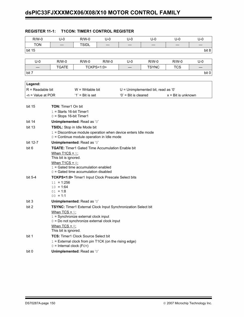
dsPIC33FJXXXMCX06/X08/X10 MOTOR CONTROL FAMILY
REGISTER 11-1: T1CON: TIMER1 CONTROL REGISTER
R/W-0 U-0 R/W-0 U-0 U-0 U-0 U-0 U-0TON — TSIDL — — — — —
bit 15 bit 8
U-0 R/W-0 R/W-0 R/W-0 U-0 R/W-0 R/W-0 U-0— TGATE TCKPS<1:0> — TSYNC TCS —
bit 7 bit 0
Legend:R = Readable bit W = Writable bit U = Unimplemented bit, read as ‘0’-n = Value at POR ‘1’ = Bit is set ‘0’ = Bit is cleared x = Bit is unknown
bit 15 TON: Timer1 On bit1 = Starts 16-bit Timer10 = Stops 16-bit Timer1
bit 14 Unimplemented: Read as ‘0’bit 13 TSIDL: Stop in Idle Mode bit
1 = Discontinue module operation when device enters Idle mode0 = Continue module operation in Idle mode
bit 12-7 Unimplemented: Read as ‘0’bit 6 TGATE: Timer1 Gated Time Accumulation Enable bit
When T1CS = 1: This bit is ignored.When T1CS = 0: 1 = Gated time accumulation enabled0 = Gated time accumulation disabled
bit 5-4 TCKPS<1:0> Timer1 Input Clock Prescale Select bits11 = 1:256 10 = 1:6401 = 1:8 00 = 1:1
bit 3 Unimplemented: Read as ‘0’bit 2 TSYNC: Timer1 External Clock Input Synchronization Select bit
When TCS = 1: 1 = Synchronize external clock input0 = Do not synchronize external clock inputWhen TCS = 0: This bit is ignored.
bit 1 TCS: Timer1 Clock Source Select bit1 = External clock from pin T1CK (on the rising edge) 0 = Internal clock (FCY)
bit 0 Unimplemented: Read as ‘0’
DS70287A-page 150 © 2007 Microchip Technology Inc.
dsPIC33FJXXXMCX06/X08/X10 MOTOR CONTROL FAMILY
12.0 TIMER2/3, TIMER4/5, TIMER6/7 AND TIMER8/9
The Timer2/3, Timer4/5, Timer6/7 and Timer8/9modules are 32-bit timers which can also be configuredas four independent 16-bit timers with selectable oper-ating modes.
As a 32-bit timer, Timer2/3, Timer4/5, Timer6/7 andTimer8/9 operate in three modes:
• Two Independent 16-bit Timers (e.g., Timer2 and Timer3) with all 16-bit operating modes (except Asynchronous Counter mode)
• Single 32-bit Timer• Single 32-bit Synchronous Counter
They also support the following features:
• Timer Gate Operation• Selectable Prescaler Settings• Timer Operation during Idle and Sleep modes• Interrupt on a 32-bit Period Register Match• Time Base for Input Capture and Output Compare
Modules (Timer2 and Timer3 only)• ADC1 Event Trigger (Timer2/3 only)• ADC2 Event Trigger (Timer4/5 only)
Individually, all eight of the 16-bit timers can function assynchronous timers or counters. They also offer thefeatures listed above, except for the event trigger; thisis implemented only with Timer2/3. The operatingmodes and enabled features are determined by settingthe appropriate bit(s) in the T2CON, T3CON, T4CON,T5CON, T6CON, T7CON, T8CON and T9CON regis-ters. T2CON, T4CON, T6CON and T8CON are shownin generic form in Register 12-1. T3CON, T5CON,T7CON and T9CON are shown in Register 12-2.
For 32-bit timer/counter operation, Timer2, Timer4,Timer6 or Timer8 is the least significant word; Timer3,Timer5, Timer7 or Timer9 is the most significant wordof the 32-bit timers.
To configure Timer2/3, Timer4/5, Timer6/7 or Timer8/9for 32-bit operation, do the following:
1. Set the corresponding T32 control bit.2. Select the prescaler ratio for Timer2, Timer4,
Timer6 or Timer8 using the TCKPS<1:0> bits.3. Set the Clock and Gating modes using the
corresponding TCS and TGATE bits.4. Load the timer period value. PR3, PR5, PR7 or
PR9 contains the most significant word of thevalue, while PR2, PR4, PR6 or PR8 contains theleast significant word.
5. If interrupts are required, set the interrupt enablebit, T3IE, T5IE, T7IE or T9IE. Use the prioritybits, T3IP<2:0>, T5IP<2:0>, T7IP<2:0> orT9IP<2:0>, to set the interrupt priority. WhileTimer2, Timer4, Timer6 or Timer8 control thetimer, the interrupt appears as a Timer3, Timer5,Timer7 or Timer9 interrupt.
6. Set the corresponding TON bit.
The timer value at any point is stored in the registerpair, TMR3:TMR2, TMR5:TMR4, TMR7:TMR6 orTMR9:TMR8. TMR3, TMR5, TMR7 or TMR9 alwayscontain the most significant word of the count, whileTMR2, TMR4, TMR6 or TMR8 contain the leastsignificant word.
To configure any of the timers for individual 16-bitoperation, do the following:
1. Clear the T32 bit corresponding to that timer.2. Select the timer prescaler ratio using the
TCKPS<1:0> bits.3. Set the Clock and Gating modes using the TCS
and TGATE bits.4. Load the timer period value into the PRx
register.5. If interrupts are required, set the interrupt enable
bit, TxIE. Use the priority bits, TxIP<2:0>, to setthe interrupt priority.
6. Set the TON bit.
A block diagram for a 32-bit timer pair (Timer4/5)example is shown in Figure 12-1, and a timer (Timer4)operating in 16-bit mode example is shown inFigure 12-2.
Note: This data sheet summarizes the featuresof this group of dsPIC33FJXXXMCX06/X08/X10 Motor Control Family devices. Itis not intended to be a comprehensivereference source. To complement theinformation in this data sheet, refer to the“dsPIC33F Family Reference Manual”.Refer to the Microchip web site(www.microchip.com) for the latestdsPIC33F family reference manualchapters.
Note: For 32-bit operation, T3CON, T5CON,T7CON and T9CON control bits areignored. Only T2CON, T4CON, T6CONand T8CON control bits are used for setupand control. Timer2, Timer4, Timer6 andTimer8 clock and gate inputs are utilizedfor the 32-bit timer modules, but an inter-rupt is generated with the Timer3, Timer5,Ttimer7 and Timer9 interrupt flags.
Note: Only Timer2 and Timer3 can trigger aDMA data transfer.
© 2007 Microchip Technology Inc. DS70287A-page 151
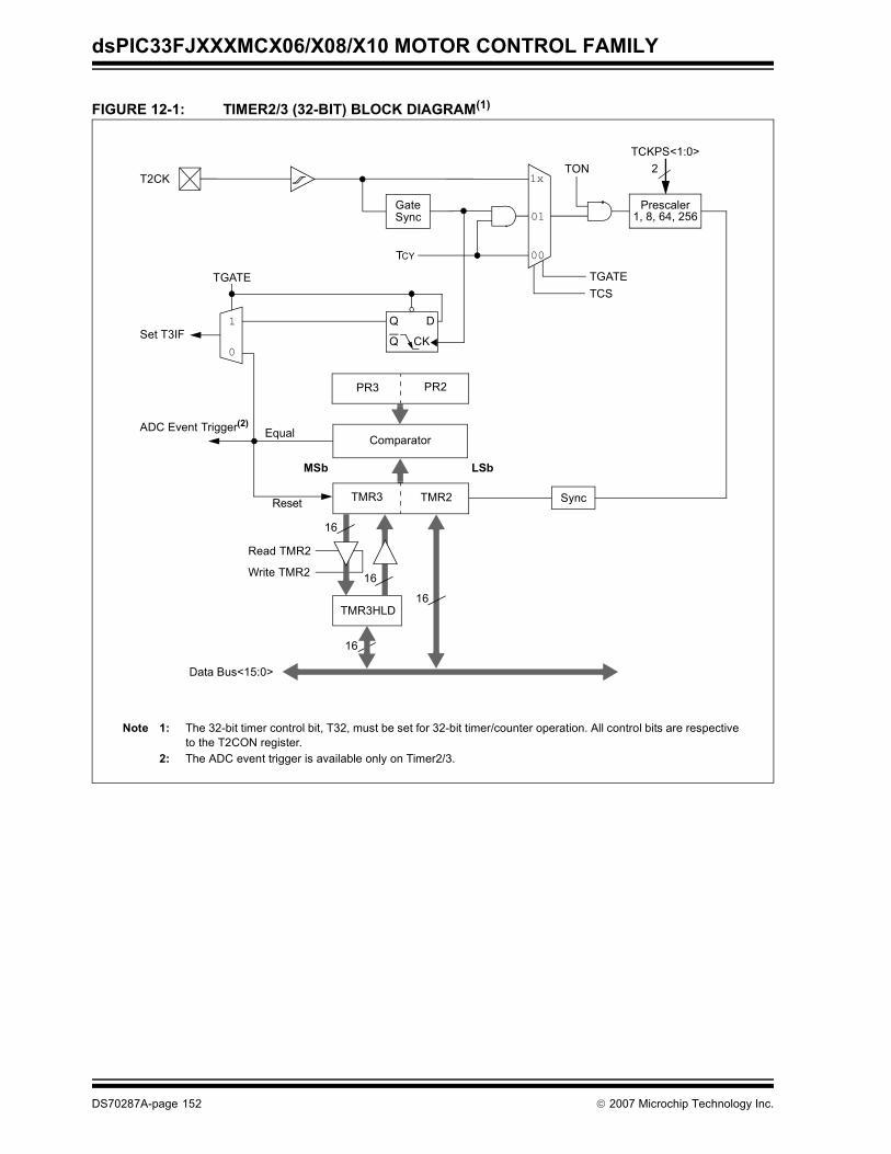
dsPIC33FJXXXMCX06/X08/X10 MOTOR CONTROL FAMILY
FIGURE 12-1: TIMER2/3 (32-BIT) BLOCK DIAGRAM(1)
Set T3IF
Equal Comparator
PR3 PR2
Reset
LSbMSb
Note 1: The 32-bit timer control bit, T32, must be set for 32-bit timer/counter operation. All control bits are respective to the T2CON register.
2: The ADC event trigger is available only on Timer2/3.
Data Bus<15:0>
TMR3HLD
Read TMR2
Write TMR2 16
16
16
Q
Q D
CK
TGATE
0
1
TON
TCKPS<1:0>2
TCY
TCS
1x
01
TGATE
00
T2CK
ADC Event Trigger(2)
GateSync
Prescaler1, 8, 64, 256
SyncTMR3 TMR2
16
DS70287A-page 152 © 2007 Microchip Technology Inc.
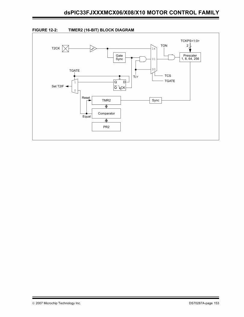
dsPIC33FJXXXMCX06/X08/X10 MOTOR CONTROL FAMILY
FIGURE 12-2: TIMER2 (16-BIT) BLOCK DIAGRAM
TON
TCKPS<1:0>
Prescaler1, 8, 64, 256
2
TCY TCSTGATE
T2CK
PR2
Set T2IF
EqualComparator
TMR2Reset
Q
Q D
CK
TGATE
1
0
GateSync
1x
01
00
Sync
© 2007 Microchip Technology Inc. DS70287A-page 153
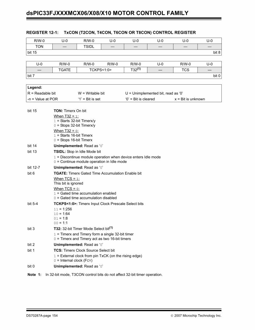
dsPIC33FJXXXMCX06/X08/X10 MOTOR CONTROL FAMILY
REGISTER 12-1: TxCON (T2CON, T4CON, T6CON OR T8CON) CONTROL REGISTER
R/W-0 U-0 R/W-0 U-0 U-0 U-0 U-0 U-0TON — TSIDL — — — — —
bit 15 bit 8
U-0 R/W-0 R/W-0 R/W-0 R/W-0 U-0 R/W-0 U-0— TGATE TCKPS<1:0> T32(1) — TCS —
bit 7 bit 0
Legend:R = Readable bit W = Writable bit U = Unimplemented bit, read as ‘0’-n = Value at POR ‘1’ = Bit is set ‘0’ = Bit is cleared x = Bit is unknown
bit 15 TON: Timerx On bitWhen T32 = 1:1 = Starts 32-bit Timerx/y0 = Stops 32-bit Timerx/yWhen T32 = 0:1 = Starts 16-bit Timerx0 = Stops 16-bit Timerx
bit 14 Unimplemented: Read as ‘0’bit 13 TSIDL: Stop in Idle Mode bit
1 = Discontinue module operation when device enters Idle mode0 = Continue module operation in Idle mode
bit 12-7 Unimplemented: Read as ‘0’bit 6 TGATE: Timerx Gated Time Accumulation Enable bit
When TCS = 1: This bit is ignoredWhen TCS = 0: 1 = Gated time accumulation enabled0 = Gated time accumulation disabled
bit 5-4 TCKPS<1:0>: Timerx Input Clock Prescale Select bits11 = 1:256 10 = 1:6401 = 1:8 00 = 1:1
bit 3 T32: 32-bit Timer Mode Select bit(1)
1 = Timerx and Timery form a single 32-bit timer0 = Timerx and Timery act as two 16-bit timers
bit 2 Unimplemented: Read as ‘0’bit 1 TCS: Timerx Clock Source Select bit
1 = External clock from pin TxCK (on the rising edge) 0 = Internal clock (FCY)
bit 0 Unimplemented: Read as ‘0’
Note 1: In 32-bit mode, T3CON control bits do not affect 32-bit timer operation.
DS70287A-page 154 © 2007 Microchip Technology Inc.
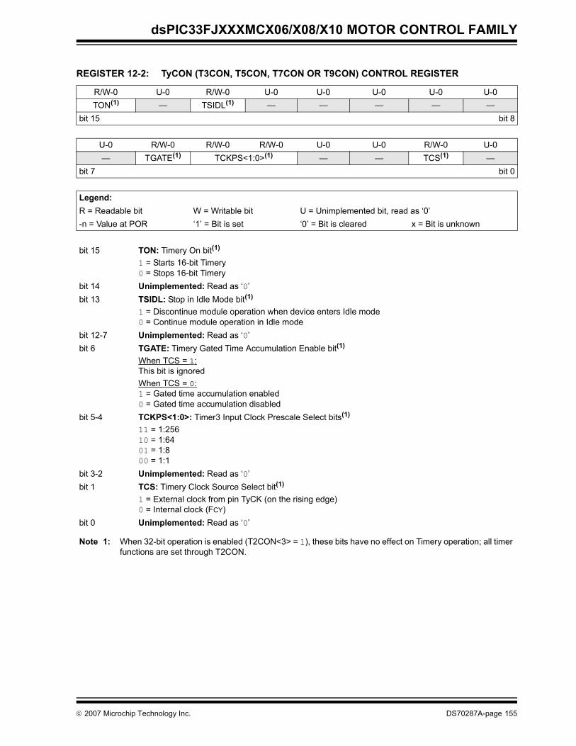
dsPIC33FJXXXMCX06/X08/X10 MOTOR CONTROL FAMILY
REGISTER 12-2: TyCON (T3CON, T5CON, T7CON OR T9CON) CONTROL REGISTER
R/W-0 U-0 R/W-0 U-0 U-0 U-0 U-0 U-0TON(1) — TSIDL(1) — — — — —
bit 15 bit 8
U-0 R/W-0 R/W-0 R/W-0 U-0 U-0 R/W-0 U-0— TGATE(1) TCKPS<1:0>(1) — — TCS(1) —
bit 7 bit 0
Legend:R = Readable bit W = Writable bit U = Unimplemented bit, read as ‘0’-n = Value at POR ‘1’ = Bit is set ‘0’ = Bit is cleared x = Bit is unknown
bit 15 TON: Timery On bit(1)
1 = Starts 16-bit Timery0 = Stops 16-bit Timery
bit 14 Unimplemented: Read as ‘0’bit 13 TSIDL: Stop in Idle Mode bit(1)
1 = Discontinue module operation when device enters Idle mode0 = Continue module operation in Idle mode
bit 12-7 Unimplemented: Read as ‘0’bit 6 TGATE: Timery Gated Time Accumulation Enable bit(1)
When TCS = 1: This bit is ignoredWhen TCS = 0: 1 = Gated time accumulation enabled0 = Gated time accumulation disabled
bit 5-4 TCKPS<1:0>: Timer3 Input Clock Prescale Select bits(1)
11 = 1:256 10 = 1:6401 = 1:8 00 = 1:1
bit 3-2 Unimplemented: Read as ‘0’bit 1 TCS: Timery Clock Source Select bit(1)
1 = External clock from pin TyCK (on the rising edge) 0 = Internal clock (FCY)
bit 0 Unimplemented: Read as ‘0’
Note 1: When 32-bit operation is enabled (T2CON<3> = 1), these bits have no effect on Timery operation; all timer functions are set through T2CON.
© 2007 Microchip Technology Inc. DS70287A-page 155

dsPIC33FJXXXMCX06/X08/X10 MOTOR CONTROL FAMILY
NOTES:
DS70287A-page 156 © 2007 Microchip Technology Inc.
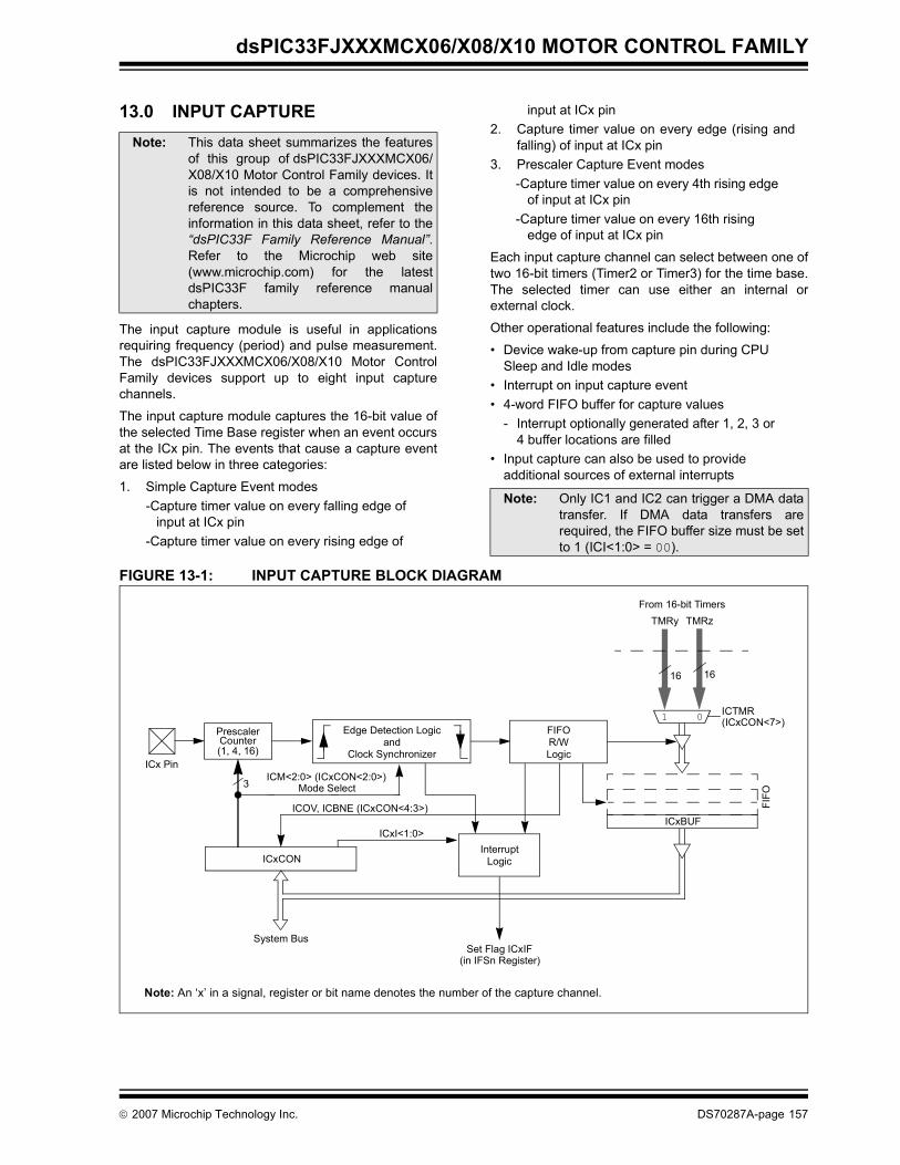
dsPIC33FJXXXMCX06/X08/X10 MOTOR CONTROL FAMILY
13.0 INPUT CAPTURE
The input capture module is useful in applicationsrequiring frequency (period) and pulse measurement.The dsPIC33FJXXXMCX06/X08/X10 Motor ControlFamily devices support up to eight input capturechannels.
The input capture module captures the 16-bit value ofthe selected Time Base register when an event occursat the ICx pin. The events that cause a capture eventare listed below in three categories:
1. Simple Capture Event modes-Capture timer value on every falling edge of
input at ICx pin-Capture timer value on every rising edge of
input at ICx pin2. Capture timer value on every edge (rising and
falling) of input at ICx pin3. Prescaler Capture Event modes
-Capture timer value on every 4th rising edge of input at ICx pin
-Capture timer value on every 16th rising edge of input at ICx pin
Each input capture channel can select between one oftwo 16-bit timers (Timer2 or Timer3) for the time base.The selected timer can use either an internal orexternal clock.
Other operational features include the following:
• Device wake-up from capture pin during CPU Sleep and Idle modes
• Interrupt on input capture event• 4-word FIFO buffer for capture values
- Interrupt optionally generated after 1, 2, 3 or 4 buffer locations are filled
• Input capture can also be used to provide additional sources of external interrupts
FIGURE 13-1: INPUT CAPTURE BLOCK DIAGRAM
Note: This data sheet summarizes the featuresof this group of dsPIC33FJXXXMCX06/X08/X10 Motor Control Family devices. Itis not intended to be a comprehensivereference source. To complement theinformation in this data sheet, refer to the“dsPIC33F Family Reference Manual”.Refer to the Microchip web site(www.microchip.com) for the latestdsPIC33F family reference manualchapters.
Note: Only IC1 and IC2 can trigger a DMA datatransfer. If DMA data transfers arerequired, the FIFO buffer size must be setto 1 (ICI<1:0> = 00).
ICxBUF
ICx PinICM<2:0> (ICxCON<2:0>)
Mode Select3
1 0
Set Flag ICxIF(in IFSn Register)
TMRy TMRz
Edge Detection Logic
16 16
FIFOR/WLogic
ICxI<1:0>
ICOV, ICBNE (ICxCON<4:3>)
ICxCONInterrupt
Logic
System Bus
From 16-bit Timers
ICTMR(ICxCON<7>)
FIFO
PrescalerCounter(1, 4, 16)
andClock Synchronizer
Note: An ‘x’ in a signal, register or bit name denotes the number of the capture channel.
© 2007 Microchip Technology Inc. DS70287A-page 157
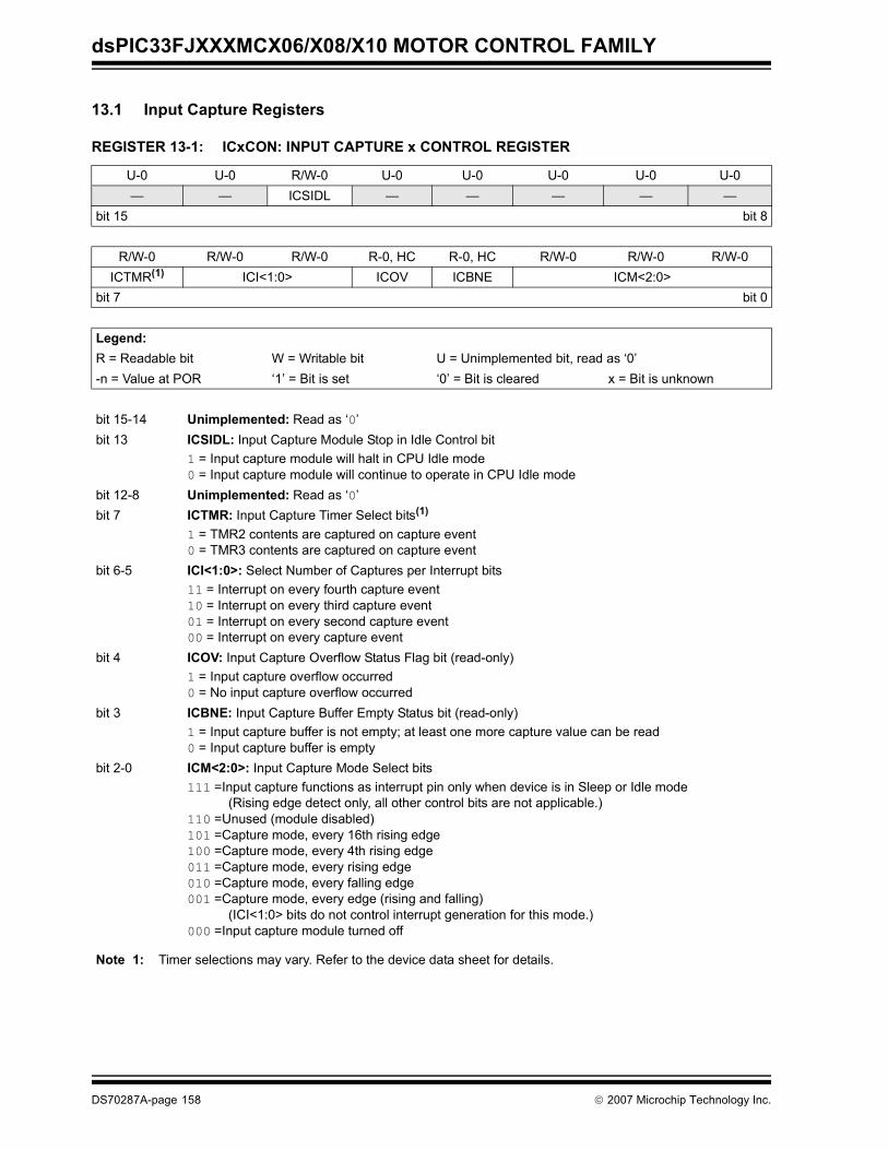
dsPIC33FJXXXMCX06/X08/X10 MOTOR CONTROL FAMILY
13.1 Input Capture Registers REGISTER 13-1: ICxCON: INPUT CAPTURE x CONTROL REGISTER
U-0 U-0 R/W-0 U-0 U-0 U-0 U-0 U-0— — ICSIDL — — — — —
bit 15 bit 8
R/W-0 R/W-0 R/W-0 R-0, HC R-0, HC R/W-0 R/W-0 R/W-0ICTMR(1) ICI<1:0> ICOV ICBNE ICM<2:0>
bit 7 bit 0
Legend:R = Readable bit W = Writable bit U = Unimplemented bit, read as ‘0’-n = Value at POR ‘1’ = Bit is set ‘0’ = Bit is cleared x = Bit is unknown
bit 15-14 Unimplemented: Read as ‘0’bit 13 ICSIDL: Input Capture Module Stop in Idle Control bit
1 = Input capture module will halt in CPU Idle mode0 = Input capture module will continue to operate in CPU Idle mode
bit 12-8 Unimplemented: Read as ‘0’bit 7 ICTMR: Input Capture Timer Select bits(1)
1 = TMR2 contents are captured on capture event0 = TMR3 contents are captured on capture event
bit 6-5 ICI<1:0>: Select Number of Captures per Interrupt bits11 = Interrupt on every fourth capture event10 = Interrupt on every third capture event01 = Interrupt on every second capture event00 = Interrupt on every capture event
bit 4 ICOV: Input Capture Overflow Status Flag bit (read-only)1 = Input capture overflow occurred0 = No input capture overflow occurred
bit 3 ICBNE: Input Capture Buffer Empty Status bit (read-only)1 = Input capture buffer is not empty; at least one more capture value can be read0 = Input capture buffer is empty
bit 2-0 ICM<2:0>: Input Capture Mode Select bits111 =Input capture functions as interrupt pin only when device is in Sleep or Idle mode
(Rising edge detect only, all other control bits are not applicable.)110 =Unused (module disabled)101 =Capture mode, every 16th rising edge100 =Capture mode, every 4th rising edge011 =Capture mode, every rising edge010 =Capture mode, every falling edge001 =Capture mode, every edge (rising and falling)
(ICI<1:0> bits do not control interrupt generation for this mode.)000 =Input capture module turned off
Note 1: Timer selections may vary. Refer to the device data sheet for details.
DS70287A-page 158 © 2007 Microchip Technology Inc.
dsPIC33FJXXXMCX06/X08/X10 MOTOR CONTROL FAMILY
14.0 OUTPUT COMPARE
14.1 Setup for Single Output Pulse Generation
When the OCM control bits (OCxCON<2:0>) are set to‘100’, the selected output compare channel initializesthe OCx pin to the low state and generates a singleoutput pulse.To generate a single output pulse, the following stepsare required (these steps assume the timer source isinitially turned off, but this is not a requirement for themodule operation):1. Determine the instruction clock cycle time. Take
into account the frequency of the external clockto the timer source (if one is used) and the timerprescaler settings.
2. Calculate time to the rising edge of the outputpulse relative to the TMRy start value (0000h).
3. Calculate the time to the falling edge of the pulse,based on the desired pulse width and the time tothe rising edge of the pulse.
4. Write the values computed in steps 2 and 3 aboveinto the Output Compare register, OCxR, and theOutput Compare Secondary register, OCxRS,respectively.
5. Set the Timer Period register, PRy, to a valueequal to or greater than the value in OCxRS, theOutput Compare Secondary register.
6. Set the OCM bits to ‘100’ and the OCTSEL(OCxCON<3>) bit to the desired timer source. TheOCx pin state will now be driven low.
7. Set the TON (TyCON<15>) bit to ‘1’, whichenables the compare time base to count.
8. Upon the first match between TMRy and OCxR,the OCx pin will be driven high.
9. When the incrementing timer, TMRy, matches theOutput Compare Secondary register, OCxRS, thesecond and trailing edge (high-to-low) of the pulseis driven onto the OCx pin. No additional pulsesare driven onto the OCx pin and it remains at low.As a result of the second compare match event,the OCxIF interrupt flag bit is set, which will resultin an interrupt if the interrupt enable bit, OCxIE, isset. For further information on peripheralinterrupts, refer to Section 6.0 “Interrupt Con-troller”.
10. To initiate another single pulse output, change theTimer and Compare register settings, if needed,
and then issue a write to set the OCM bits to ‘100’.Disabling and re-enabling the timer, and clearingthe TMRy register, are not required but may beadvantageous for defining a pulse from a knownevent time boundary.
The output compare module does not have to be dis-abled after the falling edge of the output pulse. Anotherpulse can be initiated by rewriting the value of theOCxCON register.
14.2 Setup for Continuous Output Pulse Generation
When the OCM control bits (OCxCON<2:0>) are set to‘101’, the selected output compare channel initializesthe OCx pin to the low state and generates outputpulses on each and every compare match event.For the user to configure the module for the generationof a continuous stream of output pulses, the followingsteps are required (these steps assume the timersource is initially turned off, but this is not a requirementfor the module operation):1. Determine the instruction clock cycle time. Take
into account the frequency of the external clockto the timer source (if one is used) and the timerprescaler settings.
2. Calculate time to the rising edge of the outputpulse relative to the TMRy start value (0000h).
3. Calculate the time to the falling edge of the pulse,based on the desired pulse width and the time tothe rising edge of the pulse.
4. Write the values computed in step 2 and 3 aboveinto the Output Compare register, OCxR, and theOutput Compare Secondary register, OCxRS,respectively.
5. Set the Timer Period register, PRy, to a valueequal to or greater than the value in OCxRS, theOutput Compare Secondary register.
6. Set the OCM bits to ‘101’ and the OCTSEL bit tothe desired timer source. The OCx pin state willnow be driven low.
7. Enable the compare time base by setting the TON(TyCON<15>) bit to ‘1’.
8. Upon the first match between TMRy and OCxR,the OCx pin will be driven high.
9. When the compare time base, TMRy, matchesthe Output Compare Secondary register, OCxRS,the second and trailing edge (high-to-low) of thepulse is driven onto the OCx pin.
10. As a result of the second compare match event,the OCxIF interrupt flag bit is set.
11. When the compare time base and the value in itsrespective Timer Period register match, the TMRyregister resets to 0x0000 and resumes counting.
12. Steps 8 through 11 are repeated and a continuousstream of pulses is generated, indefinitely. TheOCxIF flag is set on each OCxRS-TMRy comparematch event.
Note: This data sheet summarizes the featuresof this group of dsPIC33FJXXXMCX06/X08/X10 Motor Control Family devices. Itis not intended to be a comprehensivereference source. To complement theinformation in this data sheet, refer to the“dsPIC33F Family Reference Manual”.Refer to the Microchip web site(www.microchip.com) for the latestdsPIC33F family reference manualchapters.
© 2007 Microchip Technology Inc. DS70287A-page 159
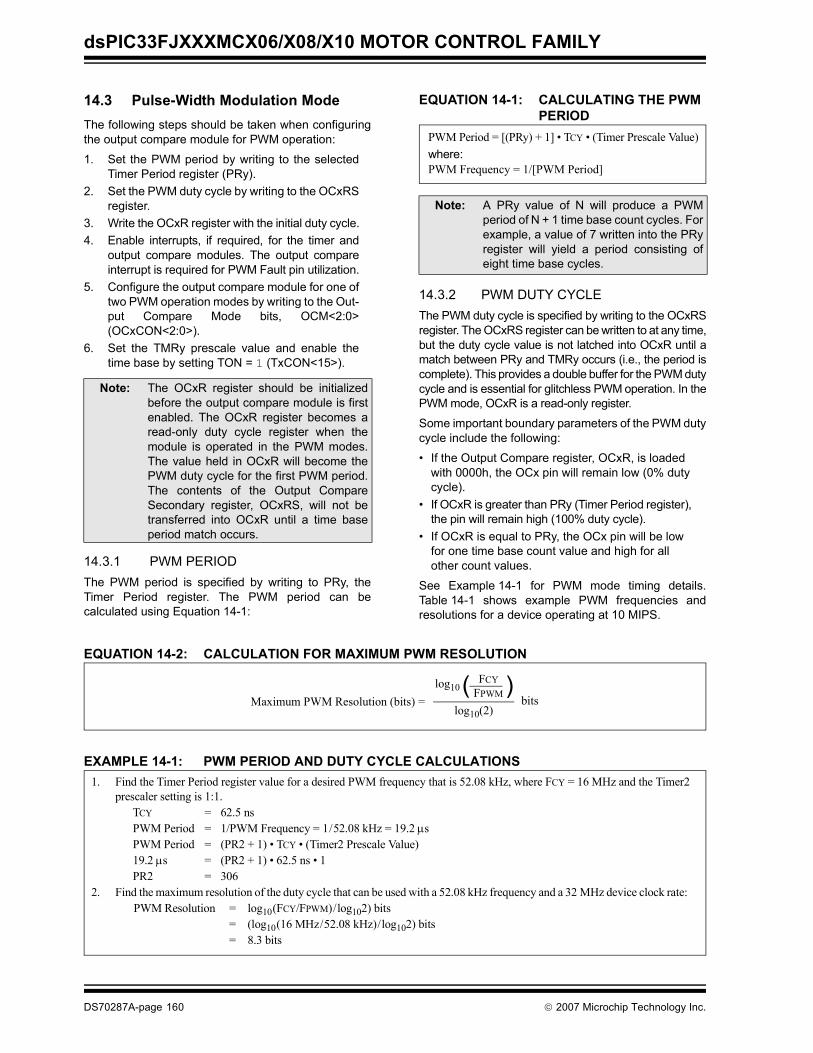
dsPIC33FJXXXMCX06/X08/X10 MOTOR CONTROL FAMILY
14.3 Pulse-Width Modulation ModeThe following steps should be taken when configuringthe output compare module for PWM operation:
1. Set the PWM period by writing to the selectedTimer Period register (PRy).
2. Set the PWM duty cycle by writing to the OCxRSregister.
3. Write the OCxR register with the initial duty cycle.4. Enable interrupts, if required, for the timer and
output compare modules. The output compareinterrupt is required for PWM Fault pin utilization.
5. Configure the output compare module for one oftwo PWM operation modes by writing to the Out-put Compare Mode bits, OCM<2:0>(OCxCON<2:0>).
6. Set the TMRy prescale value and enable thetime base by setting TON = 1 (TxCON<15>).
14.3.1 PWM PERIODThe PWM period is specified by writing to PRy, theTimer Period register. The PWM period can becalculated using Equation 14-1:
EQUATION 14-1: CALCULATING THE PWM PERIOD
14.3.2 PWM DUTY CYCLEThe PWM duty cycle is specified by writing to the OCxRSregister. The OCxRS register can be written to at any time,but the duty cycle value is not latched into OCxR until amatch between PRy and TMRy occurs (i.e., the period iscomplete). This provides a double buffer for the PWM dutycycle and is essential for glitchless PWM operation. In thePWM mode, OCxR is a read-only register.
Some important boundary parameters of the PWM dutycycle include the following:
• If the Output Compare register, OCxR, is loaded with 0000h, the OCx pin will remain low (0% duty cycle).
• If OCxR is greater than PRy (Timer Period register), the pin will remain high (100% duty cycle).
• If OCxR is equal to PRy, the OCx pin will be low for one time base count value and high for all other count values.
See Example 14-1 for PWM mode timing details.Table 14-1 shows example PWM frequencies andresolutions for a device operating at 10 MIPS.
EQUATION 14-2: CALCULATION FOR MAXIMUM PWM RESOLUTION
EXAMPLE 14-1: PWM PERIOD AND DUTY CYCLE CALCULATIONS
Note: The OCxR register should be initializedbefore the output compare module is firstenabled. The OCxR register becomes aread-only duty cycle register when themodule is operated in the PWM modes.The value held in OCxR will become thePWM duty cycle for the first PWM period.The contents of the Output CompareSecondary register, OCxRS, will not betransferred into OCxR until a time baseperiod match occurs.
Note: A PRy value of N will produce a PWMperiod of N + 1 time base count cycles. Forexample, a value of 7 written into the PRyregister will yield a period consisting ofeight time base cycles.
PWM Period = [(PRy) + 1] • TCY • (Timer Prescale Value)
PWM Frequency = 1/[PWM Period]where:
( )Maximum PWM Resolution (bits) =
FCY FPWM
log10
log10(2)bits
1. Find the Timer Period register value for a desired PWM frequency that is 52.08 kHz, where FCY = 16 MHz and the Timer2prescaler setting is 1:1.
TCY = 62.5 nsPWM Period = 1/PWM Frequency = 1/52.08 kHz = 19.2 μsPWM Period = (PR2 + 1) • TCY • (Timer2 Prescale Value)19.2 μs = (PR2 + 1) • 62.5 ns • 1 PR2 = 306
2. Find the maximum resolution of the duty cycle that can be used with a 52.08 kHz frequency and a 32 MHz device clock rate: PWM Resolution = log10(FCY/FPWM)/log102) bits
= (log10(16 MHz/52.08 kHz)/log102) bits= 8.3 bits
DS70287A-page 160 © 2007 Microchip Technology Inc.
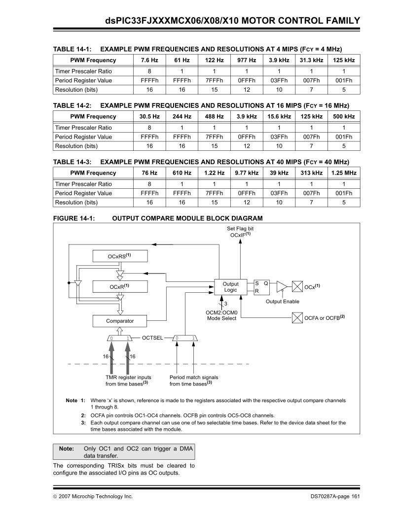
dsPIC33FJXXXMCX06/X08/X10 MOTOR CONTROL FAMILY
TABLE 14-1: EXAMPLE PWM FREQUENCIES AND RESOLUTIONS AT 4 MIPS (FCY = 4 MHz)
TABLE 14-2: EXAMPLE PWM FREQUENCIES AND RESOLUTIONS AT 16 MIPS (FCY = 16 MHz)
TABLE 14-3: EXAMPLE PWM FREQUENCIES AND RESOLUTIONS AT 40 MIPS (FCY = 40 MHz)
FIGURE 14-1: OUTPUT COMPARE MODULE BLOCK DIAGRAM
The corresponding TRISx bits must be cleared toconfigure the associated I/O pins as OC outputs.
PWM Frequency 7.6 Hz 61 Hz 122 Hz 977 Hz 3.9 kHz 31.3 kHz 125 kHz
Timer Prescaler Ratio 8 1 1 1 1 1 1Period Register Value FFFFh FFFFh 7FFFh 0FFFh 03FFh 007Fh 001FhResolution (bits) 16 16 15 12 10 7 5
PWM Frequency 30.5 Hz 244 Hz 488 Hz 3.9 kHz 15.6 kHz 125 kHz 500 kHz
Timer Prescaler Ratio 8 1 1 1 1 1 1Period Register Value FFFFh FFFFh 7FFFh 0FFFh 03FFh 007Fh 001FhResolution (bits) 16 16 15 12 10 7 5
PWM Frequency 76 Hz 610 Hz 1.22 Hz 9.77 kHz 39 kHz 313 kHz 1.25 MHz
Timer Prescaler Ratio 8 1 1 1 1 1 1Period Register Value FFFFh FFFFh 7FFFh 0FFFh 03FFh 007Fh 001FhResolution (bits) 16 16 15 12 10 7 5
Note: Only OC1 and OC2 can trigger a DMAdata transfer.
OCxR(1)
Comparator
OutputLogic
OCM2:OCM0
Output Enable
OCx(1)
Set Flag bitOCxIF(1)
OCxRS(1)
Mode Select
3
Note 1: Where ‘x’ is shown, reference is made to the registers associated with the respective output compare channels1 through 8.
2: OCFA pin controls OC1-OC4 channels. OCFB pin controls OC5-OC8 channels.3: Each output compare channel can use one of two selectable time bases. Refer to the device data sheet for the
time bases associated with the module.
OCTSEL 0 1
16 16
OCFA or OCFB(2)
TMR register inputsfrom time bases(3)
Period match signalsfrom time bases(3)
0 1
QSR
© 2007 Microchip Technology Inc. DS70287A-page 161
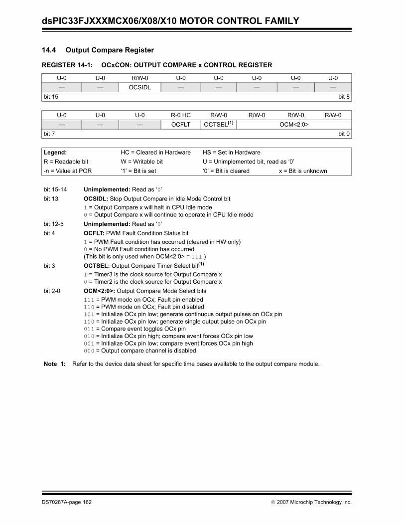
dsPIC33FJXXXMCX06/X08/X10 MOTOR CONTROL FAMILY
14.4 Output Compare Register REGISTER 14-1: OCxCON: OUTPUT COMPARE x CONTROL REGISTER
U-0 U-0 R/W-0 U-0 U-0 U-0 U-0 U-0— — OCSIDL — — — — —
bit 15 bit 8
U-0 U-0 U-0 R-0 HC R/W-0 R/W-0 R/W-0 R/W-0— — — OCFLT OCTSEL(1) OCM<2:0>
bit 7 bit 0
Legend: HC = Cleared in Hardware HS = Set in HardwareR = Readable bit W = Writable bit U = Unimplemented bit, read as ‘0’-n = Value at POR ‘1’ = Bit is set ‘0’ = Bit is cleared x = Bit is unknown
bit 15-14 Unimplemented: Read as ‘0’bit 13 OCSIDL: Stop Output Compare in Idle Mode Control bit
1 = Output Compare x will halt in CPU Idle mode0 = Output Compare x will continue to operate in CPU Idle mode
bit 12-5 Unimplemented: Read as ‘0’bit 4 OCFLT: PWM Fault Condition Status bit
1 = PWM Fault condition has occurred (cleared in HW only)0 = No PWM Fault condition has occurred(This bit is only used when OCM<2:0> = 111.)
bit 3 OCTSEL: Output Compare Timer Select bit(1)
1 = Timer3 is the clock source for Output Compare x0 = Timer2 is the clock source for Output Compare x
bit 2-0 OCM<2:0>: Output Compare Mode Select bits111 = PWM mode on OCx; Fault pin enabled110 = PWM mode on OCx; Fault pin disabled101 = Initialize OCx pin low; generate continuous output pulses on OCx pin100 = Initialize OCx pin low; generate single output pulse on OCx pin011 = Compare event toggles OCx pin010 = Initialize OCx pin high; compare event forces OCx pin low001 = Initialize OCx pin low; compare event forces OCx pin high 000 = Output compare channel is disabled
Note 1: Refer to the device data sheet for specific time bases available to the output compare module.
DS70287A-page 162 © 2007 Microchip Technology Inc.
dsPIC33FJXXXMCX06/X08/X10 MOTOR CONTROL FAMILY
15.0 MOTOR CONTROL PWM MODULE
This module simplifies the task of generating multiple,synchronized Pulse-Width Modulated (PWM) outputs.In particular, the following power and motion controlapplications are supported by the PWM module:
• 3-Phase AC Induction Motor• Switched Reluctance (SR) Motor• Brushless DC (BLDC) Motor• Uninterruptible Power Supply (UPS)
The PWM module has the following features:
• 8 PWM I/O pins with 4 duty cycle generators• Up to 16-bit resolution• ‘On-the-fly’ PWM frequency changes• Edge and Center-Aligned Output modes• Single Pulse Generation mode• Interrupt support for asymmetrical updates in
Center-Aligned mode• Output override control for Electrically
Commutative Motor (ECM) operation• ‘Special Event’ comparator for scheduling other
peripheral events • Fault pins to optionally drive each of the PWM
output pins to a defined state• Duty cycle updates are configurable to be
immediate or synchronized to the PWM time base
This module contains 4 duty cycle generators,numbered 1 through 4. The module has eight PWMoutput pins, numbered PWM1H/PWM1L throughPWM4H/PWM4L. The eight I/O pins are grouped intohigh/low numbered pairs, denoted by the suffix H or L,respectively. For complementary loads, the low PWMpins are always the complement of the correspondinghigh I/O pin.
The PWM module allows several modes of operationwhich are beneficial for specific power controlapplications.
Note: This data sheet summarizes the featuresof this group of dsPIC33FJXXXMCX06/X08/X10 Motor Control Family devices. Itis not intended to be a comprehensivereference source. To complement theinformation in this data sheet, refer to the“dsPIC33F Family ReferenceManual”.Refer to the Microchip web site(www.microchip.com) for the latestdsPIC33F family reference manualchapters.
© 2007 Microchip Technology Inc. DS70287A-page 163
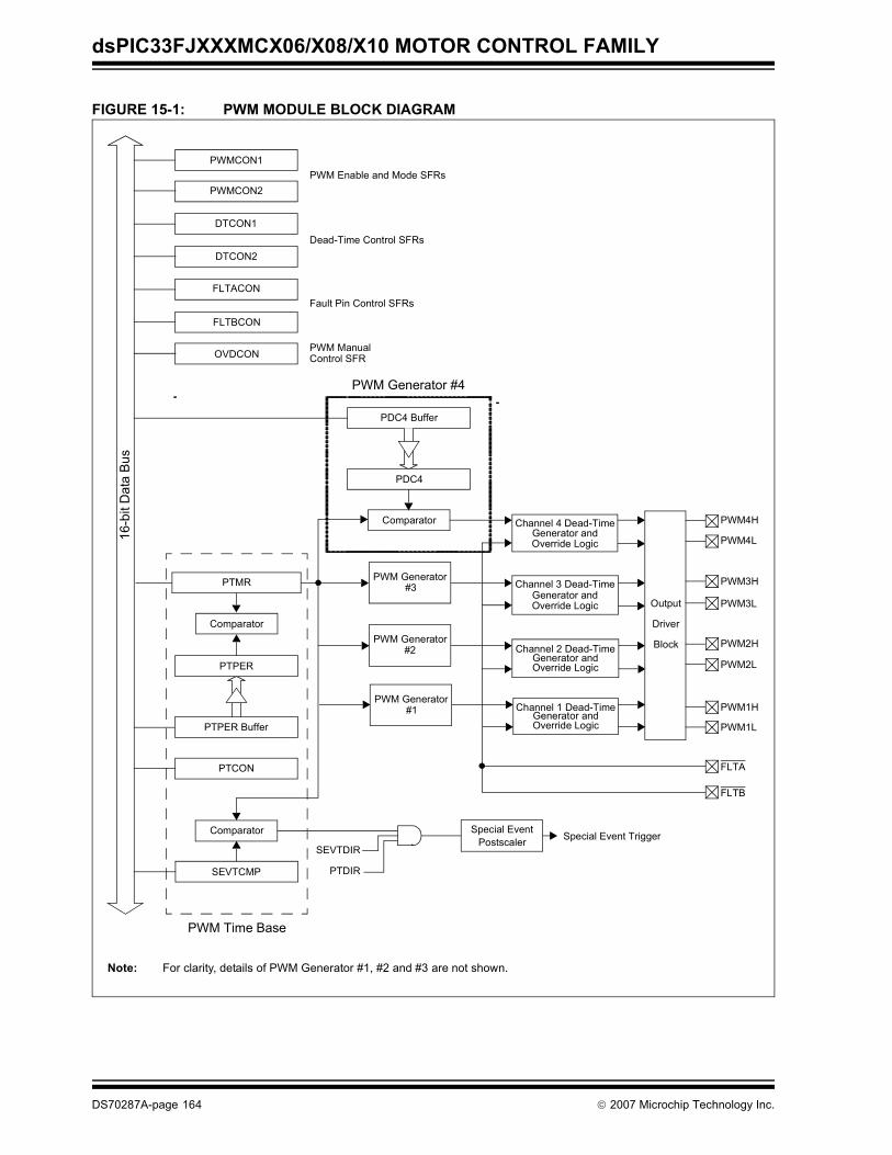
dsPIC33FJXXXMCX06/X08/X10 MOTOR CONTROL FAMILY
FIGURE 15-1: PWM MODULE BLOCK DIAGRAM
PDC4
PDC4 Buffer
PWMCON1
PWMCON2
PTPER
Comparator
Comparator
Channel 4 Dead-TimeGenerator and
PTCON
SEVTCMP
Comparator Special Event Trigger
FLTBCON
OVDCON
PWM Enable and Mode SFRs
PWM ManualControl SFR
Channel 3 Dead-TimeGenerator and
Channel 2 Dead-TimeGenerator and
PWM Generator#3
PWM Generator#2
PWM Generator #4
SEVTDIR
PTDIR
DTCON1Dead-Time Control SFRs
PWM1L
PWM1H
PWM2L
PWM2H
PWM3L
PWM3H
PWM Generator#1 Channel 1 Dead-Time
Generator and
Note: For clarity, details of PWM Generator #1, #2 and #3 are not shown.
16-b
it D
ata
Bus
PWM4L
PWM4H
DTCON2
FLTACONFault Pin Control SFRs
PWM Time Base
Output
Driver
Block
FLTB
FLTA
Override Logic
Override Logic
Override Logic
Override Logic
Special EventPostscaler
PTPER Buffer
PTMR
DS70287A-page 164 © 2007 Microchip Technology Inc.
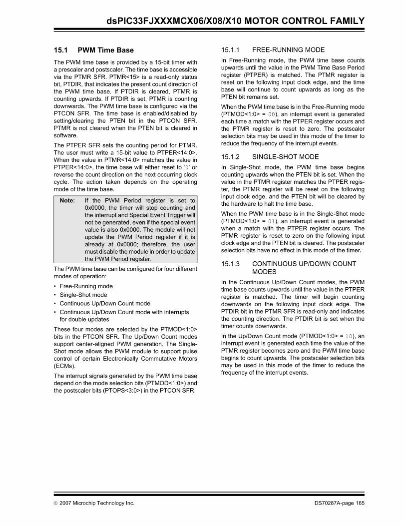
dsPIC33FJXXXMCX06/X08/X10 MOTOR CONTROL FAMILY
15.1 PWM Time BaseThe PWM time base is provided by a 15-bit timer witha prescaler and postscaler. The time base is accessiblevia the PTMR SFR. PTMR<15> is a read-only statusbit, PTDIR, that indicates the present count direction ofthe PWM time base. If PTDIR is cleared, PTMR iscounting upwards. If PTDIR is set, PTMR is countingdownwards. The PWM time base is configured via thePTCON SFR. The time base is enabled/disabled bysetting/clearing the PTEN bit in the PTCON SFR.PTMR is not cleared when the PTEN bit is cleared insoftware.
The PTPER SFR sets the counting period for PTMR.The user must write a 15-bit value to PTPER<14:0>.When the value in PTMR<14:0> matches the value inPTPER<14:0>, the time base will either reset to ‘0’ orreverse the count direction on the next occurring clockcycle. The action taken depends on the operatingmode of the time base.
The PWM time base can be configured for four differentmodes of operation:
• Free-Running mode• Single-Shot mode• Continuous Up/Down Count mode• Continuous Up/Down Count mode with interrupts
for double updates
These four modes are selected by the PTMOD<1:0>bits in the PTCON SFR. The Up/Down Count modessupport center-aligned PWM generation. The Single-Shot mode allows the PWM module to support pulsecontrol of certain Electronically Commutative Motors(ECMs).
The interrupt signals generated by the PWM time basedepend on the mode selection bits (PTMOD<1:0>) andthe postscaler bits (PTOPS<3:0>) in the PTCON SFR.
15.1.1 FREE-RUNNING MODEIn Free-Running mode, the PWM time base countsupwards until the value in the PWM Time Base Periodregister (PTPER) is matched. The PTMR register isreset on the following input clock edge, and the timebase will continue to count upwards as long as thePTEN bit remains set.
When the PWM time base is in the Free-Running mode(PTMOD<1:0> = 00), an interrupt event is generatedeach time a match with the PTPER register occurs andthe PTMR register is reset to zero. The postscalerselection bits may be used in this mode of the timer toreduce the frequency of the interrupt events.
15.1.2 SINGLE-SHOT MODEIn Single-Shot mode, the PWM time base beginscounting upwards when the PTEN bit is set. When thevalue in the PTMR register matches the PTPER regis-ter, the PTMR register will be reset on the followinginput clock edge, and the PTEN bit will be cleared bythe hardware to halt the time base.
When the PWM time base is in the Single-Shot mode(PTMOD<1:0> = 01), an interrupt event is generatedwhen a match with the PTPER register occurs. ThePTMR register is reset to zero on the following inputclock edge and the PTEN bit is cleared. The postscalerselection bits have no effect in this mode of the timer.
15.1.3 CONTINUOUS UP/DOWN COUNT MODES
In the Continuous Up/Down Count modes, the PWMtime base counts upwards until the value in the PTPERregister is matched. The timer will begin countingdownwards on the following input clock edge. ThePTDIR bit in the PTMR SFR is read-only and indicatesthe counting direction. The PTDIR bit is set when thetimer counts downwards.
In the Up/Down Count mode (PTMOD<1:0> = 10), aninterrupt event is generated each time the value of thePTMR register becomes zero and the PWM time basebegins to count upwards. The postscaler selection bitsmay be used in this mode of the timer to reduce thefrequency of the interrupt events.
Note: If the PWM Period register is set to0x0000, the timer will stop counting andthe interrupt and Special Event Trigger willnot be generated, even if the special eventvalue is also 0x0000. The module will notupdate the PWM Period register if it isalready at 0x0000; therefore, the usermust disable the module in order to updatethe PWM Period register.
© 2007 Microchip Technology Inc. DS70287A-page 165
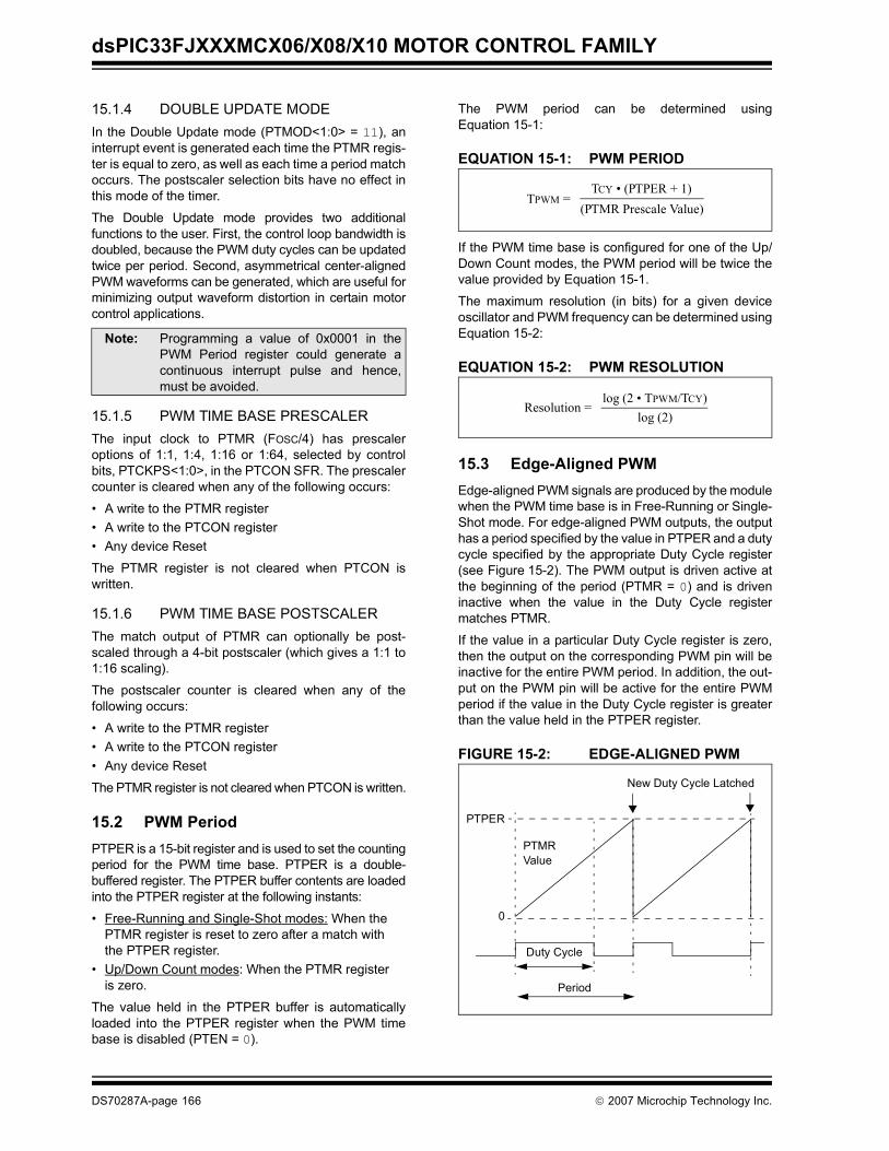
dsPIC33FJXXXMCX06/X08/X10 MOTOR CONTROL FAMILY
15.1.4 DOUBLE UPDATE MODEIn the Double Update mode (PTMOD<1:0> = 11), aninterrupt event is generated each time the PTMR regis-ter is equal to zero, as well as each time a period matchoccurs. The postscaler selection bits have no effect inthis mode of the timer.
The Double Update mode provides two additionalfunctions to the user. First, the control loop bandwidth isdoubled, because the PWM duty cycles can be updatedtwice per period. Second, asymmetrical center-alignedPWM waveforms can be generated, which are useful forminimizing output waveform distortion in certain motorcontrol applications.
15.1.5 PWM TIME BASE PRESCALERThe input clock to PTMR (FOSC/4) has prescaleroptions of 1:1, 1:4, 1:16 or 1:64, selected by controlbits, PTCKPS<1:0>, in the PTCON SFR. The prescalercounter is cleared when any of the following occurs:
• A write to the PTMR register• A write to the PTCON register• Any device Reset
The PTMR register is not cleared when PTCON iswritten.
15.1.6 PWM TIME BASE POSTSCALERThe match output of PTMR can optionally be post-scaled through a 4-bit postscaler (which gives a 1:1 to1:16 scaling).
The postscaler counter is cleared when any of thefollowing occurs:
• A write to the PTMR register• A write to the PTCON register• Any device Reset
The PTMR register is not cleared when PTCON is written.
15.2 PWM PeriodPTPER is a 15-bit register and is used to set the countingperiod for the PWM time base. PTPER is a double-buffered register. The PTPER buffer contents are loadedinto the PTPER register at the following instants:
• Free-Running and Single-Shot modes: When the PTMR register is reset to zero after a match with the PTPER register.
• Up/Down Count modes: When the PTMR register is zero.
The value held in the PTPER buffer is automaticallyloaded into the PTPER register when the PWM timebase is disabled (PTEN = 0).
The PWM period can be determined usingEquation 15-1:
EQUATION 15-1: PWM PERIOD
If the PWM time base is configured for one of the Up/Down Count modes, the PWM period will be twice thevalue provided by Equation 15-1.
The maximum resolution (in bits) for a given deviceoscillator and PWM frequency can be determined usingEquation 15-2:
EQUATION 15-2: PWM RESOLUTION
15.3 Edge-Aligned PWM Edge-aligned PWM signals are produced by the modulewhen the PWM time base is in Free-Running or Single-Shot mode. For edge-aligned PWM outputs, the outputhas a period specified by the value in PTPER and a dutycycle specified by the appropriate Duty Cycle register(see Figure 15-2). The PWM output is driven active atthe beginning of the period (PTMR = 0) and is driveninactive when the value in the Duty Cycle registermatches PTMR.
If the value in a particular Duty Cycle register is zero,then the output on the corresponding PWM pin will beinactive for the entire PWM period. In addition, the out-put on the PWM pin will be active for the entire PWMperiod if the value in the Duty Cycle register is greaterthan the value held in the PTPER register.
FIGURE 15-2: EDGE-ALIGNED PWM
Note: Programming a value of 0x0001 in thePWM Period register could generate acontinuous interrupt pulse and hence,must be avoided.
TPWM =TCY • (PTPER + 1)
(PTMR Prescale Value)
Resolution =log (2 • TPWM/TCY)
log (2)
Period
Duty Cycle
0
PTPER
PTMRValue
New Duty Cycle Latched
DS70287A-page 166 © 2007 Microchip Technology Inc.
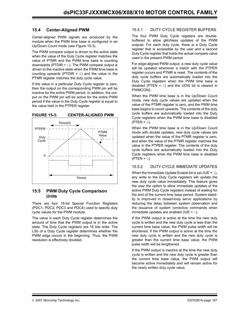
dsPIC33FJXXXMCX06/X08/X10 MOTOR CONTROL FAMILY
15.4 Center-Aligned PWMCenter-aligned PWM signals are produced by themodule when the PWM time base is configured in anUp/Down Count mode (see Figure 15-3).
The PWM compare output is driven to the active statewhen the value of the Duty Cycle register matches thevalue of PTMR and the PWM time base is countingdownwards (PTDIR = 1). The PWM compare output isdriven to the inactive state when the PWM time base iscounting upwards (PTDIR = 0) and the value in thePTMR register matches the duty cycle value.
If the value in a particular Duty Cycle register is zero,then the output on the corresponding PWM pin will beinactive for the entire PWM period. In addition, the out-put on the PWM pin will be active for the entire PWMperiod if the value in the Duty Cycle register is equal tothe value held in the PTPER register.
FIGURE 15-3: CENTER-ALIGNED PWM
15.5 PWM Duty Cycle Comparison Units
There are four 16-bit Special Function Registers(PDC1, PDC2, PDC3 and PDC4) used to specify dutycycle values for the PWM module.
The value in each Duty Cycle register determines theamount of time that the PWM output is in the activestate. The Duty Cycle registers are 16 bits wide. TheLSb of a Duty Cycle register determines whether thePWM edge occurs in the beginning. Thus, the PWMresolution is effectively doubled.
15.5.1 DUTY CYCLE REGISTER BUFFERSThe four PWM Duty Cycle registers are double-buffered to allow glitchless updates of the PWMoutputs. For each duty cycle, there is a Duty Cycleregister that is accessible by the user and a secondDuty Cycle register that holds the actual compare valueused in the present PWM period.
For edge-aligned PWM output, a new duty cycle valuewill be updated whenever a match with the PTPERregister occurs and PTMR is reset. The contents of theduty cycle buffers are automatically loaded into theDuty Cycle registers when the PWM time base isdisabled (PTEN = 0) and the UDIS bit is cleared inPWMCON2.
When the PWM time base is in the Up/Down Countmode, new duty cycle values are updated when thevalue of the PTMR register is zero, and the PWM timebase begins to count upwards. The contents of the dutycycle buffers are automatically loaded into the DutyCycle registers when the PWM time base is disabled(PTEN = 0).
When the PWM time base is in the Up/Down Countmode with double updates, new duty cycle values areupdated when the value of the PTMR register is zero,and when the value of the PTMR register matches thevalue in the PTPER register. The contents of the dutycycle buffers are automatically loaded into the DutyCycle registers when the PWM time base is disabled(PTEN = 0).
15.5.2 DUTY CYCLE IMMEDIATE UPDATESWhen the Immediate Update Enable bit is set (IUE = 1),any write to the Duty Cycle registers will update thenew duty cycle value immediately. This feature givesthe user the option to allow immediate updates of theactive PWM Duty Cycle registers instead of waiting forthe end of the current time base period. System stabil-ity is improved in closed-loop servo applications byreducing the delay between system observation andthe issuance of system corrective commands whenimmediate updates are enabled (IUE = 1).
If the PWM output is active at the time the new dutycycle is written and the new duty cycle is less than thecurrent time base value, the PWM pulse width will beshortened. If the PWM output is active at the time thenew duty cycle is written and the new duty cycle isgreater than the current time base value, the PWMpulse width will be lengthened.
If the PWM output is inactive at the time the new dutycycle is written and the new duty cycle is greater thanthe current time base value, the PWM output willbecome active immediately and will remain active forthe newly written duty cycle value.
0
PTPERPTMRValue
Period
Period/2
DutyCycle
© 2007 Microchip Technology Inc. DS70287A-page 167
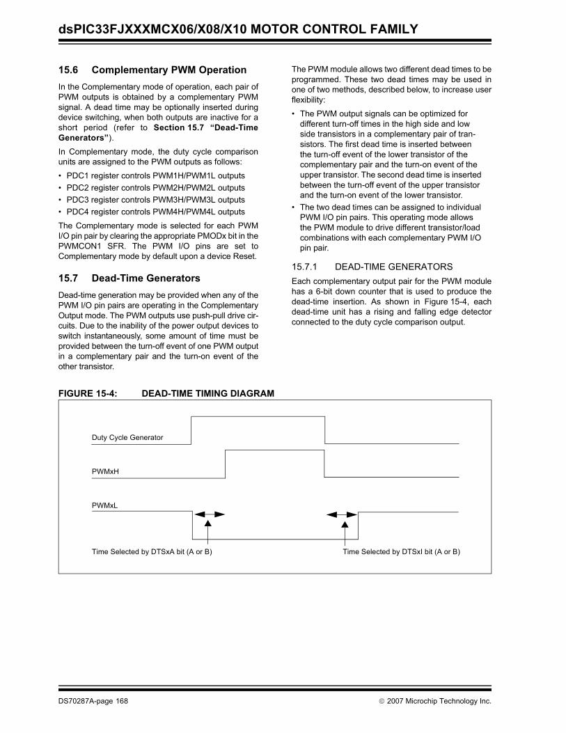
dsPIC33FJXXXMCX06/X08/X10 MOTOR CONTROL FAMILY
15.6 Complementary PWM OperationIn the Complementary mode of operation, each pair ofPWM outputs is obtained by a complementary PWMsignal. A dead time may be optionally inserted duringdevice switching, when both outputs are inactive for ashort period (refer to Section 15.7 “Dead-TimeGenerators”).
In Complementary mode, the duty cycle comparisonunits are assigned to the PWM outputs as follows:
• PDC1 register controls PWM1H/PWM1L outputs• PDC2 register controls PWM2H/PWM2L outputs• PDC3 register controls PWM3H/PWM3L outputs• PDC4 register controls PWM4H/PWM4L outputs
The Complementary mode is selected for each PWMI/O pin pair by clearing the appropriate PMODx bit in thePWMCON1 SFR. The PWM I/O pins are set toComplementary mode by default upon a device Reset.
15.7 Dead-Time GeneratorsDead-time generation may be provided when any of thePWM I/O pin pairs are operating in the ComplementaryOutput mode. The PWM outputs use push-pull drive cir-cuits. Due to the inability of the power output devices toswitch instantaneously, some amount of time must beprovided between the turn-off event of one PWM outputin a complementary pair and the turn-on event of theother transistor.
The PWM module allows two different dead times to beprogrammed. These two dead times may be used inone of two methods, described below, to increase userflexibility:
• The PWM output signals can be optimized for different turn-off times in the high side and low side transistors in a complementary pair of tran-sistors. The first dead time is inserted between the turn-off event of the lower transistor of the complementary pair and the turn-on event of the upper transistor. The second dead time is inserted between the turn-off event of the upper transistor and the turn-on event of the lower transistor.
• The two dead times can be assigned to individual PWM I/O pin pairs. This operating mode allows the PWM module to drive different transistor/load combinations with each complementary PWM I/O pin pair.
15.7.1 DEAD-TIME GENERATORSEach complementary output pair for the PWM modulehas a 6-bit down counter that is used to produce thedead-time insertion. As shown in Figure 15-4, eachdead-time unit has a rising and falling edge detectorconnected to the duty cycle comparison output.
FIGURE 15-4: DEAD-TIME TIMING DIAGRAM
Duty Cycle Generator
PWMxH
PWMxL
Time Selected by DTSxA bit (A or B) Time Selected by DTSxI bit (A or B)
DS70287A-page 168 © 2007 Microchip Technology Inc.
dsPIC33FJXXXMCX06/X08/X10 MOTOR CONTROL FAMILY
15.7.2 DEAD-TIME ASSIGNMENTThe DTCON2 SFR contains control bits that allow thedead times to be assigned to each of the complemen-tary outputs. Table 15-1 summarizes the function ofeach dead-time selection control bit.
TABLE 15-1: DEAD-TIME SELECTION BITS
15.7.3 DEAD-TIME RANGESThe amount of dead time provided by each dead-timeunit is selected by specifying the input clock prescalervalue and a 6-bit unsigned value. The amount of deadtime provided by each unit may be set independently.
Four input clock prescaler selections have been pro-vided to allow a suitable range of dead times, based onthe device operating frequency. The clock prescaleroption may be selected independently for each of thetwo dead-time values. The dead-time clock prescalervalues are selected using the DTAPS<1:0> andDTBPS<1:0> control bits in the DTCON1 SFR. One offour clock prescaler options (TCY, 2 TCY, 4 TCY or 8 TCY)may be selected for each of the dead-time values.
After the prescaler values are selected, the dead timefor each unit is adjusted by loading two 6-bit unsignedvalues into the DTCON1 SFR.
The dead-time unit prescalers are cleared on thefollowing events:
• On a load of the down timer due to a duty cycle comparison edge event.
• On a write to the DTCON1 or DTCON2 registers.• On any device Reset.
15.8 Independent PWM OutputAn Independent PWM Output mode is required fordriving certain types of loads. A particular PWM outputpair is in the Independent Output mode when the cor-responding PMODx bit in the PWMCON1 register isset. No dead-time control is implemented betweenadjacent PWM I/O pins when the module is operatingin the Independent PWM Output mode and both I/Opins are allowed to be active simultaneously.
In the Independent PWM Output mode, each duty cyclegenerator is connected to both of the PWM I/O pins inan output pair. By using the associated Duty Cycle reg-ister and the appropriate bits in the OVDCON register,the user may select the following signal output optionsfor each PWM I/O pin operating in this mode:
• I/O pin outputs PWM signal• I/O pin inactive• I/O pin active
15.9 Single Pulse PWM OperationThe PWM module produces single pulse outputs whenthe PTCON control bits PTMOD<1:0> = 10. Only edge-aligned outputs may be produced in the Single Pulsemode. In Single Pulse mode, the PWM I/O pin(s) aredriven to the active state when the PTEN bit is set.When a match with a Duty Cycle register occurs, thePWM I/O pin is driven to the inactive state. When amatch with the PTPER register occurs, the PTMRregister is cleared, all active PWM I/O pins are drivento the inactive state, the PTEN bit is cleared and aninterrupt is generated.
15.10 PWM Output OverrideThe PWM output override bits allow the user to manu-ally drive the PWM I/O pins to specified logic states,independent of the duty cycle comparison units.
All control bits associated with the PWM output over-ride function are contained in the OVDCON register.The upper half of the OVDCON register contains eightbits, POVDxH<4:1> and POVDxL<4:1>, that determinewhich PWM I/O pins will be overridden. The lower halfof the OVDCON register contains eight bits,POUTxH<4:1> and POUTxL<4:1>, that determine thestate of the PWM I/O pins when a particular output isoverridden via the POVD bits.
15.10.1 COMPLEMENTARY OUTPUT MODEWhen a PWMxL pin is driven active via the OVDCONregister, the output signal is forced to be the comple-ment of the corresponding PWMxH pin in the pair.Dead-time insertion is still performed when PWMchannels are overridden manually.
Bit Function
DTS1A Selects PWM1L/PWM1H active edge dead time.DTS1I Selects PWM1L/PWM1H inactive edge
dead time.DTS2A Selects PWM2L/PWM2H active edge dead time.DTS2I Selects PWM2L/PWM2H inactive edge
dead time.DTS3A Selects PWM3L/PWM3H active edge dead time.DTS3I Selects PWM3L/PWM3H inactive edge
dead time.DTS4A Selects PWM4L/PWM4H active edge dead time.DTS4I Selects PWM4L/PWM4H inactive edge
dead time.
Note: The user should not modify the DTCON1or DTCON2 values while the PWM mod-ule is operating (PTEN = 1). Unexpectedresults may occur.
© 2007 Microchip Technology Inc. DS70287A-page 169
dsPIC33FJXXXMCX06/X08/X10 MOTOR CONTROL FAMILY
15.10.2 OVERRIDE SYNCHRONIZATIONIf the OSYNC bit in the PWMCON2 register is set, alloutput overrides performed via the OVDCON registerare synchronized to the PWM time base. Synchronousoutput overrides occur at the following times:
• Edge-Aligned mode – when PTMR is zero• Center-Aligned modes – when PTMR is zero and
the value of PTMR matches PTPER
15.11 PWM Output and Polarity ControlThere are three device Configuration bits associatedwith the PWM module that provide PWM output pincontrol:
• HPOL Configuration bit• LPOL Configuration bit• PWMPIN Configuration bit
These three bits in the FPOR Configuration register(see Section 22.0 “Special Features”) work in con-junction with the eight PWM Enable bits (PENxH<4:1>,PENxL<4:1>) located in the PWMCON1 SFR. TheConfiguration bits and PWM Enable bits ensure thatthe PWM pins are in the correct states after a deviceReset occurs. The PWMPIN configuration fuse allowsthe PWM module outputs to be optionally enabled on adevice Reset. If PWMPIN = 0, the PWM outputs will bedriven to their inactive states at Reset. If PWMPIN = 1(default), the PWM outputs will be tri-stated. The HPOLbit specifies the polarity for the PWMxH outputs,whereas the LPOL bit specifies the polarity for thePWMxL outputs.
15.11.1 OUTPUT PIN CONTROLThe PENxH<4:1> and PENxL<4:1> control bits in thePWMCON1 SFR enable each high PWM output pinand each low PWM output pin, respectively. If a partic-ular PWM output pin is not enabled, it is treated as ageneral purpose I/O pin.
15.12 PWM Fault PinsThere are two Fault pins (FLTA and FLTB) associatedwith the PWM module. When asserted, these pins canoptionally drive each of the PWM I/O pins to a definedstate.
15.12.1 FAULT PIN ENABLE BITSThe FLTACON and FLTBCON SFRs each have fourcontrol bits that determine whether a particular pair ofPWM I/O pins is to be controlled by the Fault input pin.To enable a specific PWM I/O pin pair for Faultoverrides, the corresponding bit should be set in theFLTACON or FLTBCON register.
If all enable bits are cleared in the FLTACON orFLTBCON register, then the corresponding Fault inputpin has no effect on the PWM module and the pin maybe used as a general purpose interrupt or I/O pin.
15.12.2 FAULT STATESThe FLTACON and FLTBCON Special FunctionRegisters have eight bits each that determine the stateof each PWM I/O pin when it is overridden by a Faultinput. When these bits are cleared, the PWM I/O pin isdriven to the inactive state. If the bit is set, the PWMI/O pin will be driven to the active state. The activeand inactive states are referenced to the polaritydefined for each PWM I/O pin (HPOL and LPOLpolarity control bits).
A special case exists when a PWM module I/O pair isin the Complementary mode and both pins are pro-grammed to be active on a Fault condition. ThePWMxH pin always has priority in the Complementarymode so that both I/O pins cannot be driven activesimultaneously.
15.12.3 FAULT PIN PRIORITYIf both Fault input pins have been assigned to control aparticular PWM I/O pin, the Fault state programmed forthe Fault A input pin will take priority over the Fault Binput pin.
Note: The Fault pin logic can operate indepen-dent of the PWM logic. If all the enable bitsin the FLTACON/FLTBCON registers arecleared, then the Fault pin(s) could beused as general purpose interrupt pin(s).Each Fault pin has an interrupt vector,interrupt flag bit and interrupt priority bitsassociated with it.
DS70287A-page 170 © 2007 Microchip Technology Inc.
dsPIC33FJXXXMCX06/X08/X10 MOTOR CONTROL FAMILY
15.12.4 FAULT INPUT MODESEach of the Fault input pins have two modes ofoperation:
• Latched Mode: When the Fault pin is driven low, the PWM outputs will go to the states defined in the FLTACON/FLTBCON registers. The PWM outputs will remain in this state until the Fault pin is driven high and the corresponding interrupt flag has been cleared in software. When both of these actions have occurred, the PWM outputs will return to normal operation at the beginning of the next PWM cycle or half-cycle boundary. If the interrupt flag is cleared before the Fault condition ends, the PWM module will wait until the Fault pin is no longer asserted to restore the outputs.
• Cycle-by-Cycle Mode: When the Fault input pin is driven low, the PWM outputs remain in the defined Fault states for as long as the Fault pin is held low. After the Fault pin is driven high, the PWM outputs return to normal operation at the beginning of the following PWM cycle or half-cycle boundary.
The operating mode for each Fault input pin is selectedusing the FLTAM and FLTBM control bits in theFLTACON and FLTBCON Special Function Registers.
Each of the Fault pins can be controlled manually insoftware.
15.13 PWM Update LockoutFor a complex PWM application, the user may need towrite up to four Duty Cycle registers and the PWM TimeBase Period register, PTPER, at a given time. In someapplications, it is important that all buffer registers bewritten before the new duty cycle and period values areloaded for use by the module.
The PWM update lockout feature is enabled by settingthe UDIS control bit in the PWMCON2 SFR. The UDISbit affects all Duty Cycle Buffer registers and the PWMTime Base Period register, PTPER. No duty cyclechanges or period value changes will have effect whileUDIS = 1.
If the IUE bit is set, any change to the Duty Cycleregisters will be immediately updated regardless of theUDIS bit state. The PWM Period register (PTPER)updates are not affected by the IUE control bit.
15.14 PWM Special Event TriggerThe PWM module has a Special Event Trigger thatallows ADC conversions to be synchronized to thePWM time base. The ADC sampling and conversiontime may be programmed to occur at any point withinthe PWM period. The Special Event Trigger allows theuser to minimize the delay between the time when ADCconversion results are acquired and the time when theduty cycle value is updated.
The PWM Special Event Trigger has an SFR, namedSEVTCMP, and five control bits to control its operation.The PTMR value for which a Special Event Triggershould occur is loaded into the SEVTCMP register.When the PWM time base is in an Up/Down Countmode, an additional control bit is required to specify thecounting phase for the Special Event Trigger. Thecount phase is selected using the SEVTDIR control bitin the SEVTCMP SFR. If the SEVTDIR bit is cleared,the Special Event Trigger will occur on the upwardcounting cycle of the PWM time base. If the SEVTDIRbit is set, the Special Event Trigger will occur on thedownward count cycle of the PWM time base. TheSEVTDIR control bit has no effect unless the PWM timebase is configured for an Up/Down Count mode.
15.14.1 SPECIAL EVENT TRIGGER POSTSCALER
The PWM Special Event Trigger has a postscaler thatallows a 1:1 to 1:16 postscale ratio. The postscaler isconfigured by writing the SEVOPS<3:0> control bits inthe PWMCON2 SFR.
The special event output postscaler is cleared on thefollowing events:
• Any write to the SEVTCMP register• Any device Reset
15.15 PWM Operation During CPU Sleep Mode
The Fault A and Fault B input pins have the ability towake the CPU from Sleep mode. The PWM modulegenerates an interrupt if either of the Fault pins isdriven low while in Sleep.
15.16 PWM Operation During CPU Idle Mode
The PTCON SFR contains a PTSIDL control bit. Thisbit determines if the PWM module will continue tooperate or stop when the device enters Idle mode. IfPTSIDL = 0, the module will continue to operate. IfPTSIDL = 1, the module will stop operation as long asthe CPU remains in Idle mode.
© 2007 Microchip Technology Inc. DS70287A-page 171
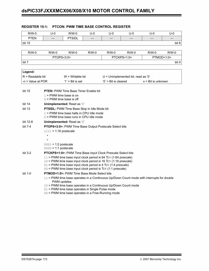
dsPIC33FJXXXMCX06/X08/X10 MOTOR CONTROL FAMILY
REGISTER 15-1: PTCON: PWM TIME BASE CONTROL REGISTER
R/W-0 U-0 R/W-0 U-0 U-0 U-0 U-0 U-0PTEN — PTSIDL — — — — —
bit 15 bit 8
R/W-0 R/W-0 R/W-0 R/W-0 R/W-0 R/W-0 R/W-0 R/W-0PTOPS<3:0> PTCKPS<1:0> PTMOD<1:0>
bit 7 bit 0
Legend:R = Readable bit W = Writable bit U = Unimplemented bit, read as ‘0’-n = Value at POR ‘1’ = Bit is set ‘0’ = Bit is cleared x = Bit is unknown
bit 15 PTEN: PWM Time Base Timer Enable bit1 = PWM time base is on0 = PWM time base is off
bit 14 Unimplemented: Read as ‘0’bit 13 PTSIDL: PWM Time Base Stop in Idle Mode bit
1 = PWM time base halts in CPU Idle mode0 = PWM time base runs in CPU Idle mode
bit 12-8 Unimplemented: Read as ‘0’bit 7-4 PTOPS<3:0>: PWM Time Base Output Postscale Select bits
1111 = 1:16 postscale••
0001 = 1:2 postscale0000 = 1:1 postscale
bit 3-2 PTCKPS<1:0>: PWM Time Base Input Clock Prescale Select bits11 = PWM time base input clock period is 64 TCY (1:64 prescale)10 = PWM time base input clock period is 16 TCY (1:16 prescale)01 = PWM time base input clock period is 4 TCY (1:4 prescale)00 = PWM time base input clock period is TCY (1:1 prescale)
bit 1-0 PTMOD<1:0>: PWM Time Base Mode Select bits11 = PWM time base operates in a Continuous Up/Down Count mode with interrupts for double
PWM updates10 = PWM time base operates in a Continuous Up/Down Count mode01 = PWM time base operates in Single Pulse mode00 = PWM time base operates in a Free-Running mode
DS70287A-page 172 © 2007 Microchip Technology Inc.
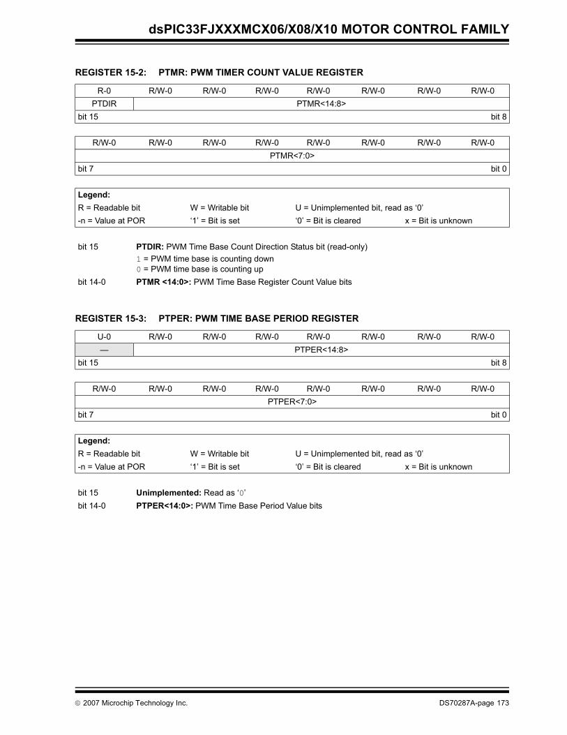
dsPIC33FJXXXMCX06/X08/X10 MOTOR CONTROL FAMILY
REGISTER 15-2: PTMR: PWM TIMER COUNT VALUE REGISTER
R-0 R/W-0 R/W-0 R/W-0 R/W-0 R/W-0 R/W-0 R/W-0PTDIR PTMR<14:8>
bit 15 bit 8
R/W-0 R/W-0 R/W-0 R/W-0 R/W-0 R/W-0 R/W-0 R/W-0PTMR<7:0>
bit 7 bit 0
Legend:R = Readable bit W = Writable bit U = Unimplemented bit, read as ‘0’-n = Value at POR ‘1’ = Bit is set ‘0’ = Bit is cleared x = Bit is unknown
bit 15 PTDIR: PWM Time Base Count Direction Status bit (read-only)1 = PWM time base is counting down0 = PWM time base is counting up
bit 14-0 PTMR <14:0>: PWM Time Base Register Count Value bits
REGISTER 15-3: PTPER: PWM TIME BASE PERIOD REGISTER
U-0 R/W-0 R/W-0 R/W-0 R/W-0 R/W-0 R/W-0 R/W-0— PTPER<14:8>
bit 15 bit 8
R/W-0 R/W-0 R/W-0 R/W-0 R/W-0 R/W-0 R/W-0 R/W-0PTPER<7:0>
bit 7 bit 0
Legend:R = Readable bit W = Writable bit U = Unimplemented bit, read as ‘0’-n = Value at POR ‘1’ = Bit is set ‘0’ = Bit is cleared x = Bit is unknown
bit 15 Unimplemented: Read as ‘0’bit 14-0 PTPER<14:0>: PWM Time Base Period Value bits
© 2007 Microchip Technology Inc. DS70287A-page 173
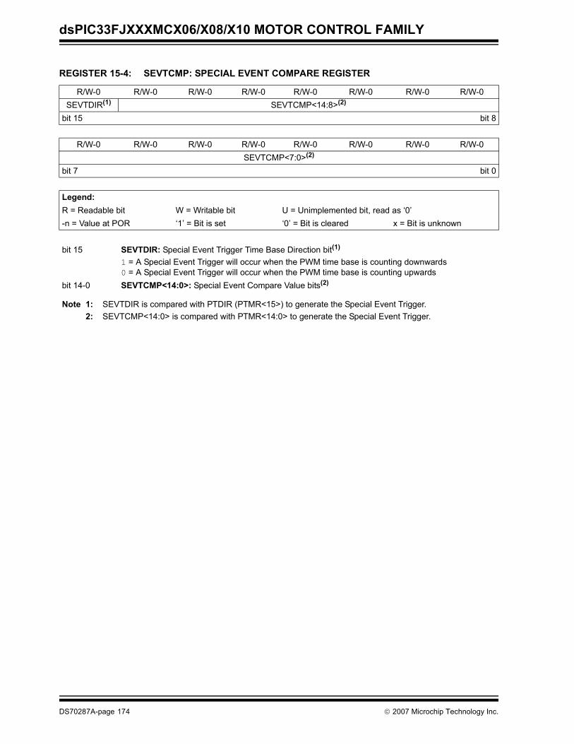
dsPIC33FJXXXMCX06/X08/X10 MOTOR CONTROL FAMILY
REGISTER 15-4: SEVTCMP: SPECIAL EVENT COMPARE REGISTER
R/W-0 R/W-0 R/W-0 R/W-0 R/W-0 R/W-0 R/W-0 R/W-0SEVTDIR(1) SEVTCMP<14:8>(2)
bit 15 bit 8
R/W-0 R/W-0 R/W-0 R/W-0 R/W-0 R/W-0 R/W-0 R/W-0SEVTCMP<7:0>(2)
bit 7 bit 0
Legend:R = Readable bit W = Writable bit U = Unimplemented bit, read as ‘0’-n = Value at POR ‘1’ = Bit is set ‘0’ = Bit is cleared x = Bit is unknown
bit 15 SEVTDIR: Special Event Trigger Time Base Direction bit(1)
1 = A Special Event Trigger will occur when the PWM time base is counting downwards0 = A Special Event Trigger will occur when the PWM time base is counting upwards
bit 14-0 SEVTCMP<14:0>: Special Event Compare Value bits(2)
Note 1: SEVTDIR is compared with PTDIR (PTMR<15>) to generate the Special Event Trigger.2: SEVTCMP<14:0> is compared with PTMR<14:0> to generate the Special Event Trigger.
DS70287A-page 174 © 2007 Microchip Technology Inc.
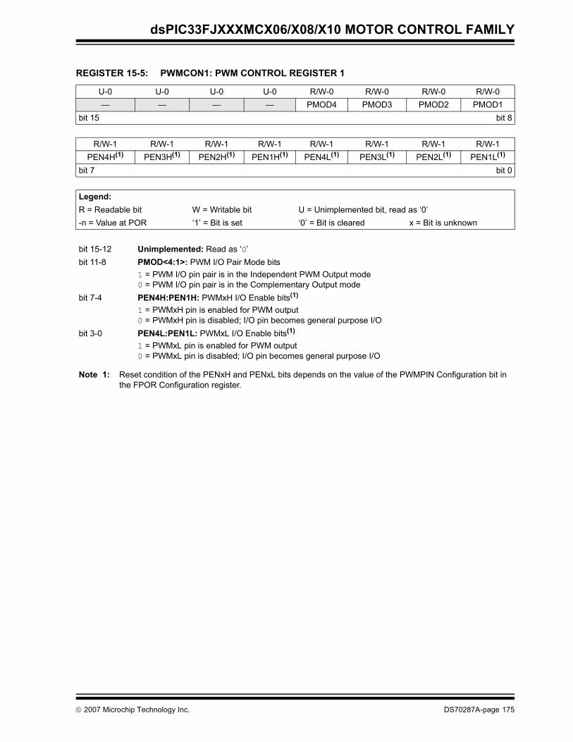
dsPIC33FJXXXMCX06/X08/X10 MOTOR CONTROL FAMILY
REGISTER 15-5: PWMCON1: PWM CONTROL REGISTER 1
U-0 U-0 U-0 U-0 R/W-0 R/W-0 R/W-0 R/W-0— — — — PMOD4 PMOD3 PMOD2 PMOD1
bit 15 bit 8
R/W-1 R/W-1 R/W-1 R/W-1 R/W-1 R/W-1 R/W-1 R/W-1PEN4H(1) PEN3H(1) PEN2H(1) PEN1H(1) PEN4L(1) PEN3L(1) PEN2L(1) PEN1L(1)
bit 7 bit 0
Legend:R = Readable bit W = Writable bit U = Unimplemented bit, read as ‘0’-n = Value at POR ‘1’ = Bit is set ‘0’ = Bit is cleared x = Bit is unknown
bit 15-12 Unimplemented: Read as ‘0’bit 11-8 PMOD<4:1>: PWM I/O Pair Mode bits
1 = PWM I/O pin pair is in the Independent PWM Output mode0 = PWM I/O pin pair is in the Complementary Output mode
bit 7-4 PEN4H:PEN1H: PWMxH I/O Enable bits(1)
1 = PWMxH pin is enabled for PWM output0 = PWMxH pin is disabled; I/O pin becomes general purpose I/O
bit 3-0 PEN4L:PEN1L: PWMxL I/O Enable bits(1)
1 = PWMxL pin is enabled for PWM output0 = PWMxL pin is disabled; I/O pin becomes general purpose I/O
Note 1: Reset condition of the PENxH and PENxL bits depends on the value of the PWMPIN Configuration bit in the FPOR Configuration register.
© 2007 Microchip Technology Inc. DS70287A-page 175
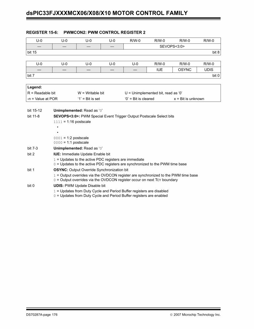
dsPIC33FJXXXMCX06/X08/X10 MOTOR CONTROL FAMILY
REGISTER 15-6: PWMCON2: PWM CONTROL REGISTER 2
U-0 U-0 U-0 U-0 R/W-0 R/W-0 R/W-0 R/W-0— — — — SEVOPS<3:0>
bit 15 bit 8
U-0 U-0 U-0 U-0 U-0 R/W-0 R/W-0 R/W-0— — — — — IUE OSYNC UDIS
bit 7 bit 0
Legend:R = Readable bit W = Writable bit U = Unimplemented bit, read as ‘0’-n = Value at POR ‘1’ = Bit is set ‘0’ = Bit is cleared x = Bit is unknown
bit 15-12 Unimplemented: Read as ‘0’bit 11-8 SEVOPS<3:0>: PWM Special Event Trigger Output Postscale Select bits
1111 = 1:16 postscale••
0001 = 1:2 postscale0000 = 1:1 postscale
bit 7-3 Unimplemented: Read as ‘0’bit 2 IUE: Immediate Update Enable bit
1 = Updates to the active PDC registers are immediate0 = Updates to the active PDC registers are synchronized to the PWM time base
bit 1 OSYNC: Output Override Synchronization bit1 = Output overrides via the OVDCON register are synchronized to the PWM time base0 = Output overrides via the OVDCON register occur on next TCY boundary
bit 0 UDIS: PWM Update Disable bit1 = Updates from Duty Cycle and Period Buffer registers are disabled0 = Updates from Duty Cycle and Period Buffer registers are enabled
DS70287A-page 176 © 2007 Microchip Technology Inc.
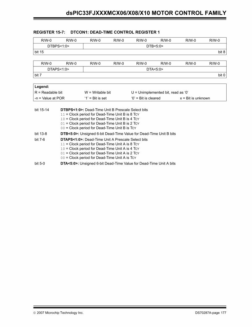
dsPIC33FJXXXMCX06/X08/X10 MOTOR CONTROL FAMILY
REGISTER 15-7: DTCON1: DEAD-TIME CONTROL REGISTER 1
R/W-0 R/W-0 R/W-0 R/W-0 R/W-0 R/W-0 R/W-0 R/W-0DTBPS<1:0> DTB<5:0>
bit 15 bit 8
R/W-0 R/W-0 R/W-0 R/W-0 R/W-0 R/W-0 R/W-0 R/W-0DTAPS<1:0> DTA<5:0>
bit 7 bit 0
Legend:R = Readable bit W = Writable bit U = Unimplemented bit, read as ‘0’-n = Value at POR ‘1’ = Bit is set ‘0’ = Bit is cleared x = Bit is unknown
bit 15-14 DTBPS<1:0>: Dead-Time Unit B Prescale Select bits11 = Clock period for Dead-Time Unit B is 8 TCY10 = Clock period for Dead-Time Unit B is 4 TCY01 = Clock period for Dead-Time Unit B is 2 TCY00 = Clock period for Dead-Time Unit B is TCY
bit 13-8 DTB<5:0>: Unsigned 6-bit Dead-Time Value for Dead-Time Unit B bitsbit 7-6 DTAPS<1:0>: Dead-Time Unit A Prescale Select bits
11 = Clock period for Dead-Time Unit A is 8 TCY10 = Clock period for Dead-Time Unit A is 4 TCY01 = Clock period for Dead-Time Unit A is 2 TCY00 = Clock period for Dead-Time Unit A is TCY
bit 5-0 DTA<5:0>: Unsigned 6-bit Dead-Time Value for Dead-Time Unit A bits
© 2007 Microchip Technology Inc. DS70287A-page 177
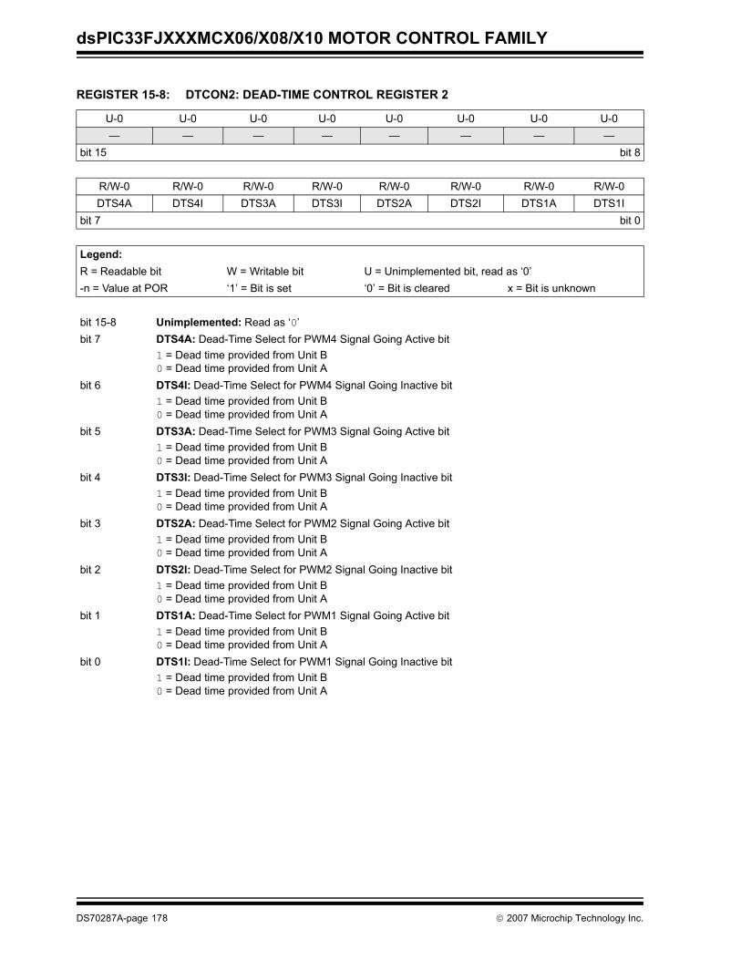
dsPIC33FJXXXMCX06/X08/X10 MOTOR CONTROL FAMILY
REGISTER 15-8: DTCON2: DEAD-TIME CONTROL REGISTER 2
U-0 U-0 U-0 U-0 U-0 U-0 U-0 U-0— — — — — — — —
bit 15 bit 8
R/W-0 R/W-0 R/W-0 R/W-0 R/W-0 R/W-0 R/W-0 R/W-0DTS4A DTS4I DTS3A DTS3I DTS2A DTS2I DTS1A DTS1I
bit 7 bit 0
Legend:R = Readable bit W = Writable bit U = Unimplemented bit, read as ‘0’-n = Value at POR ‘1’ = Bit is set ‘0’ = Bit is cleared x = Bit is unknown
bit 15-8 Unimplemented: Read as ‘0’bit 7 DTS4A: Dead-Time Select for PWM4 Signal Going Active bit
1 = Dead time provided from Unit B0 = Dead time provided from Unit A
bit 6 DTS4I: Dead-Time Select for PWM4 Signal Going Inactive bit1 = Dead time provided from Unit B0 = Dead time provided from Unit A
bit 5 DTS3A: Dead-Time Select for PWM3 Signal Going Active bit1 = Dead time provided from Unit B0 = Dead time provided from Unit A
bit 4 DTS3I: Dead-Time Select for PWM3 Signal Going Inactive bit1 = Dead time provided from Unit B0 = Dead time provided from Unit A
bit 3 DTS2A: Dead-Time Select for PWM2 Signal Going Active bit1 = Dead time provided from Unit B0 = Dead time provided from Unit A
bit 2 DTS2I: Dead-Time Select for PWM2 Signal Going Inactive bit1 = Dead time provided from Unit B0 = Dead time provided from Unit A
bit 1 DTS1A: Dead-Time Select for PWM1 Signal Going Active bit1 = Dead time provided from Unit B0 = Dead time provided from Unit A
bit 0 DTS1I: Dead-Time Select for PWM1 Signal Going Inactive bit1 = Dead time provided from Unit B0 = Dead time provided from Unit A
DS70287A-page 178 © 2007 Microchip Technology Inc.
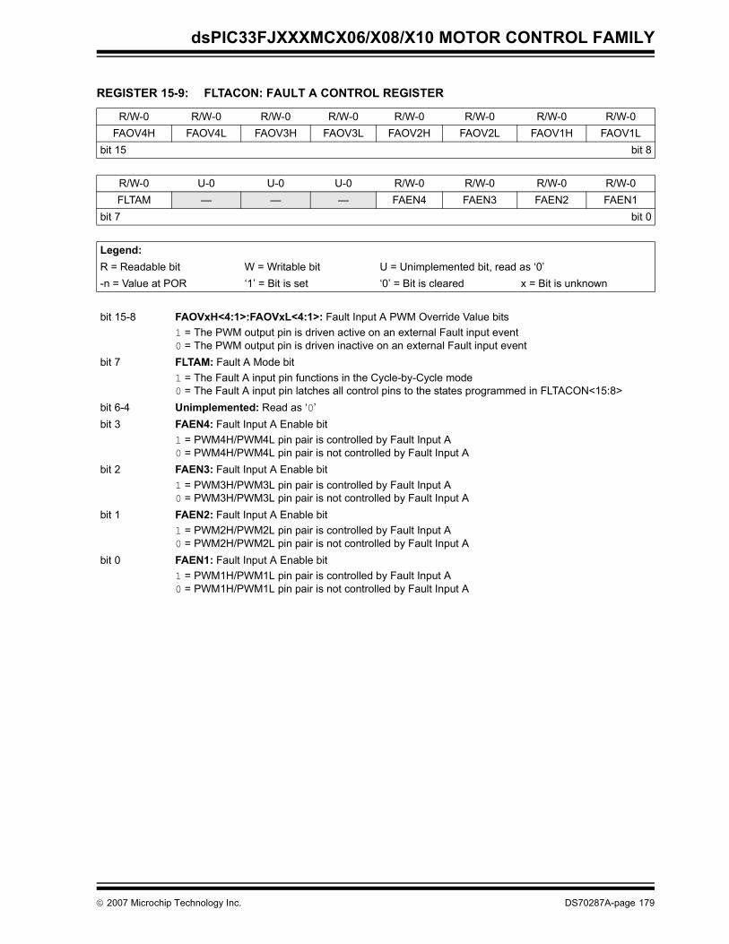
dsPIC33FJXXXMCX06/X08/X10 MOTOR CONTROL FAMILY
REGISTER 15-9: FLTACON: FAULT A CONTROL REGISTER
R/W-0 R/W-0 R/W-0 R/W-0 R/W-0 R/W-0 R/W-0 R/W-0FAOV4H FAOV4L FAOV3H FAOV3L FAOV2H FAOV2L FAOV1H FAOV1L
bit 15 bit 8
R/W-0 U-0 U-0 U-0 R/W-0 R/W-0 R/W-0 R/W-0FLTAM — — — FAEN4 FAEN3 FAEN2 FAEN1
bit 7 bit 0
Legend:R = Readable bit W = Writable bit U = Unimplemented bit, read as ‘0’-n = Value at POR ‘1’ = Bit is set ‘0’ = Bit is cleared x = Bit is unknown
bit 15-8 FAOVxH<4:1>:FAOVxL<4:1>: Fault Input A PWM Override Value bits1 = The PWM output pin is driven active on an external Fault input event0 = The PWM output pin is driven inactive on an external Fault input event
bit 7 FLTAM: Fault A Mode bit1 = The Fault A input pin functions in the Cycle-by-Cycle mode0 = The Fault A input pin latches all control pins to the states programmed in FLTACON<15:8>
bit 6-4 Unimplemented: Read as ‘0’bit 3 FAEN4: Fault Input A Enable bit
1 = PWM4H/PWM4L pin pair is controlled by Fault Input A0 = PWM4H/PWM4L pin pair is not controlled by Fault Input A
bit 2 FAEN3: Fault Input A Enable bit1 = PWM3H/PWM3L pin pair is controlled by Fault Input A0 = PWM3H/PWM3L pin pair is not controlled by Fault Input A
bit 1 FAEN2: Fault Input A Enable bit1 = PWM2H/PWM2L pin pair is controlled by Fault Input A0 = PWM2H/PWM2L pin pair is not controlled by Fault Input A
bit 0 FAEN1: Fault Input A Enable bit1 = PWM1H/PWM1L pin pair is controlled by Fault Input A0 = PWM1H/PWM1L pin pair is not controlled by Fault Input A
© 2007 Microchip Technology Inc. DS70287A-page 179
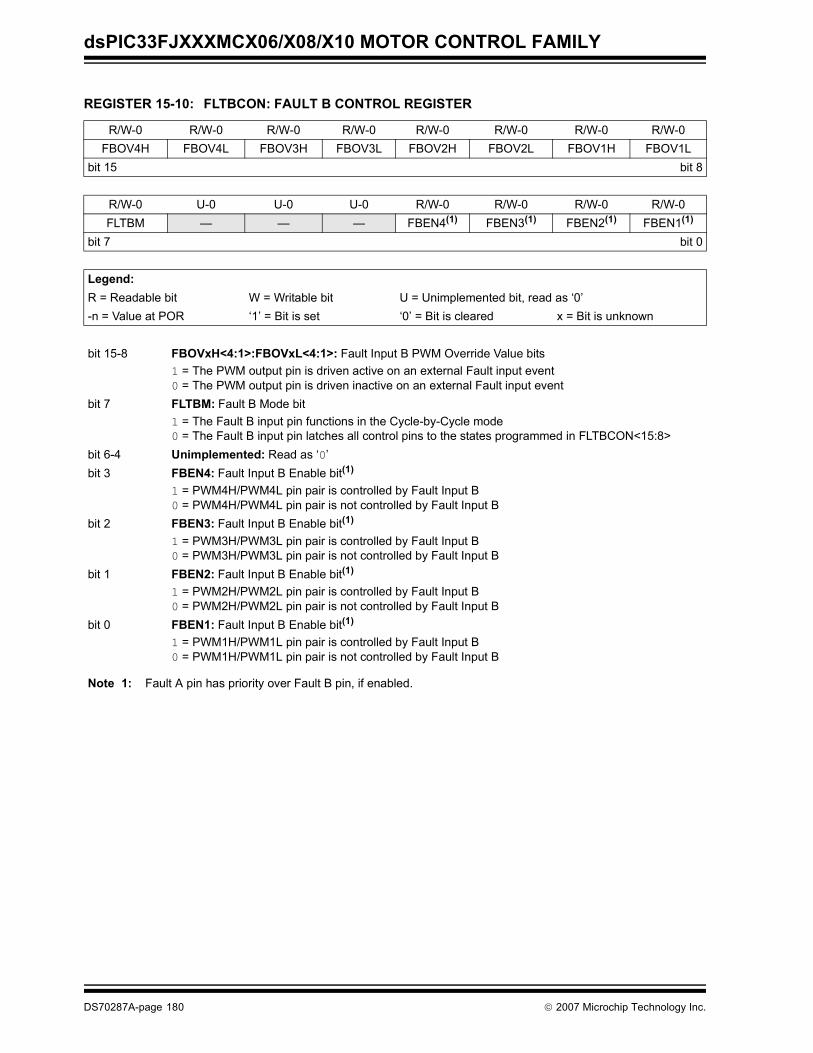
dsPIC33FJXXXMCX06/X08/X10 MOTOR CONTROL FAMILY
REGISTER 15-10: FLTBCON: FAULT B CONTROL REGISTER
R/W-0 R/W-0 R/W-0 R/W-0 R/W-0 R/W-0 R/W-0 R/W-0FBOV4H FBOV4L FBOV3H FBOV3L FBOV2H FBOV2L FBOV1H FBOV1L
bit 15 bit 8
R/W-0 U-0 U-0 U-0 R/W-0 R/W-0 R/W-0 R/W-0FLTBM — — — FBEN4(1) FBEN3(1) FBEN2(1) FBEN1(1)
bit 7 bit 0
Legend:R = Readable bit W = Writable bit U = Unimplemented bit, read as ‘0’-n = Value at POR ‘1’ = Bit is set ‘0’ = Bit is cleared x = Bit is unknown
bit 15-8 FBOVxH<4:1>:FBOVxL<4:1>: Fault Input B PWM Override Value bits1 = The PWM output pin is driven active on an external Fault input event0 = The PWM output pin is driven inactive on an external Fault input event
bit 7 FLTBM: Fault B Mode bit1 = The Fault B input pin functions in the Cycle-by-Cycle mode0 = The Fault B input pin latches all control pins to the states programmed in FLTBCON<15:8>
bit 6-4 Unimplemented: Read as ‘0’bit 3 FBEN4: Fault Input B Enable bit(1)
1 = PWM4H/PWM4L pin pair is controlled by Fault Input B0 = PWM4H/PWM4L pin pair is not controlled by Fault Input B
bit 2 FBEN3: Fault Input B Enable bit(1)
1 = PWM3H/PWM3L pin pair is controlled by Fault Input B0 = PWM3H/PWM3L pin pair is not controlled by Fault Input B
bit 1 FBEN2: Fault Input B Enable bit(1)
1 = PWM2H/PWM2L pin pair is controlled by Fault Input B0 = PWM2H/PWM2L pin pair is not controlled by Fault Input B
bit 0 FBEN1: Fault Input B Enable bit(1)
1 = PWM1H/PWM1L pin pair is controlled by Fault Input B0 = PWM1H/PWM1L pin pair is not controlled by Fault Input B
Note 1: Fault A pin has priority over Fault B pin, if enabled.
DS70287A-page 180 © 2007 Microchip Technology Inc.
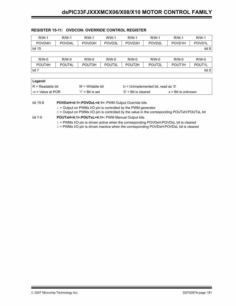
dsPIC33FJXXXMCX06/X08/X10 MOTOR CONTROL FAMILY
REGISTER 15-11: OVDCON: OVERRIDE CONTROL REGISTER
R/W-1 R/W-1 R/W-1 R/W-1 R/W-1 R/W-1 R/W-1 R/W-1POVD4H POVD4L POVD3H POVD3L POVD2H POVD2L POVD1H POVD1L
bit 15 bit 8
R/W-0 R/W-0 R/W-0 R/W-0 R/W-0 R/W-0 R/W-0 R/W-0POUT4H POUT4L POUT3H POUT3L POUT2H POUT2L POUT1H POUT1L
bit 7 bit 0
Legend:R = Readable bit W = Writable bit U = Unimplemented bit, read as ‘0’-n = Value at POR ‘1’ = Bit is set ‘0’ = Bit is cleared x = Bit is unknown
bit 15-8 POVDxH<4:1>:POVDxL<4:1>: PWM Output Override bits1 = Output on PWMx I/O pin is controlled by the PWM generator0 = Output on PWMx I/O pin is controlled by the value in the corresponding POUTxH:POUTxL bit
bit 7-0 POUTxH<4:1>:POUTxL<4:1>: PWM Manual Output bits1 = PWMx I/O pin is driven active when the corresponding POVDxH:POVDxL bit is cleared0 = PWMx I/O pin is driven inactive when the corresponding POVDxH:POVDxL bit is cleared
© 2007 Microchip Technology Inc. DS70287A-page 181
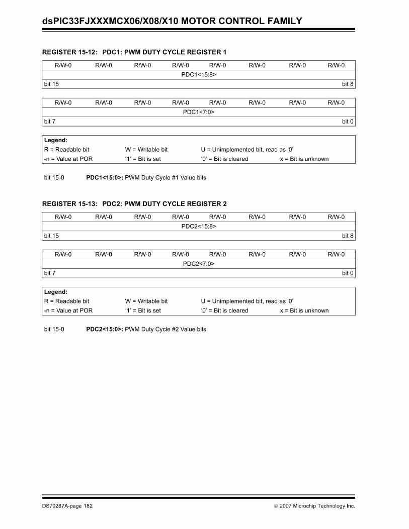
dsPIC33FJXXXMCX06/X08/X10 MOTOR CONTROL FAMILY
REGISTER 15-12: PDC1: PWM DUTY CYCLE REGISTER 1
R/W-0 R/W-0 R/W-0 R/W-0 R/W-0 R/W-0 R/W-0 R/W-0PDC1<15:8>
bit 15 bit 8
R/W-0 R/W-0 R/W-0 R/W-0 R/W-0 R/W-0 R/W-0 R/W-0PDC1<7:0>
bit 7 bit 0
Legend:R = Readable bit W = Writable bit U = Unimplemented bit, read as ‘0’-n = Value at POR ‘1’ = Bit is set ‘0’ = Bit is cleared x = Bit is unknown
bit 15-0 PDC1<15:0>: PWM Duty Cycle #1 Value bits
REGISTER 15-13: PDC2: PWM DUTY CYCLE REGISTER 2
R/W-0 R/W-0 R/W-0 R/W-0 R/W-0 R/W-0 R/W-0 R/W-0PDC2<15:8>
bit 15 bit 8
R/W-0 R/W-0 R/W-0 R/W-0 R/W-0 R/W-0 R/W-0 R/W-0PDC2<7:0>
bit 7 bit 0
Legend:R = Readable bit W = Writable bit U = Unimplemented bit, read as ‘0’-n = Value at POR ‘1’ = Bit is set ‘0’ = Bit is cleared x = Bit is unknown
bit 15-0 PDC2<15:0>: PWM Duty Cycle #2 Value bits
DS70287A-page 182 © 2007 Microchip Technology Inc.
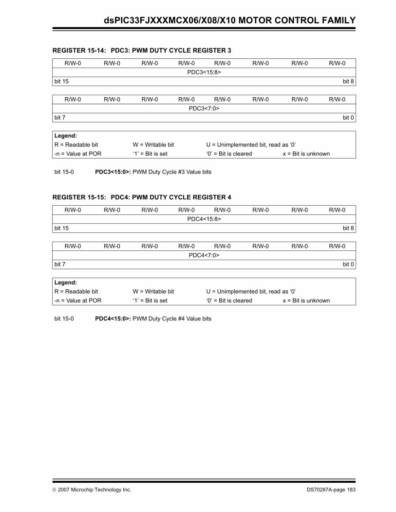
dsPIC33FJXXXMCX06/X08/X10 MOTOR CONTROL FAMILY
REGISTER 15-14: PDC3: PWM DUTY CYCLE REGISTER 3
R/W-0 R/W-0 R/W-0 R/W-0 R/W-0 R/W-0 R/W-0 R/W-0PDC3<15:8>
bit 15 bit 8
R/W-0 R/W-0 R/W-0 R/W-0 R/W-0 R/W-0 R/W-0 R/W-0PDC3<7:0>
bit 7 bit 0
Legend:R = Readable bit W = Writable bit U = Unimplemented bit, read as ‘0’-n = Value at POR ‘1’ = Bit is set ‘0’ = Bit is cleared x = Bit is unknown
bit 15-0 PDC3<15:0>: PWM Duty Cycle #3 Value bits
REGISTER 15-15: PDC4: PWM DUTY CYCLE REGISTER 4
R/W-0 R/W-0 R/W-0 R/W-0 R/W-0 R/W-0 R/W-0 R/W-0PDC4<15:8>
bit 15 bit 8
R/W-0 R/W-0 R/W-0 R/W-0 R/W-0 R/W-0 R/W-0 R/W-0PDC4<7:0>
bit 7 bit 0
Legend:R = Readable bit W = Writable bit U = Unimplemented bit, read as ‘0’-n = Value at POR ‘1’ = Bit is set ‘0’ = Bit is cleared x = Bit is unknown
bit 15-0 PDC4<15:0>: PWM Duty Cycle #4 Value bits
© 2007 Microchip Technology Inc. DS70287A-page 183

dsPIC33FJXXXMCX06/X08/X10 MOTOR CONTROL FAMILY
NOTES:
DS70287A-page 184 © 2007 Microchip Technology Inc.
dsPIC33FJXXXMCX06/X08/X10 MOTOR CONTROL FAMILY
16.0 QUADRATURE ENCODER INTERFACE (QEI) MODULE
This section describes the Quadrature Encoder Inter-face (QEI) module and associated operational modes.The QEI module provides the interface to incrementalencoders for obtaining mechanical position data.
The operational features of the QEI include the follow-ing:
• Three input channels for two phase signals and an index pulse
• 16-bit up/down position counter• Count direction status• Position Measurement (x2 and x4) mode• Programmable digital noise filters on inputs
FIGURE 16-1: QUADRATURE ENCODER INTERFACE BLOCK DIAGRAM
Note: This data sheet summarizes the featuresof this group of dsPIC33FJXXXMCX06/X08/X10 Motor Control Family devices. Itis not intended to be a comprehensive ref-erence source. To complement the infor-mation in this data sheet, refer to the“dsPIC33F Family Reference Manual”.Refer to the Microchip web site(www.microchip.com) for the latestdsPIC33F family reference manualchapters.
16-bit Up/Down Counter
Comparator/
Max Count Register
QEA
INDX
0
1Up/Down
Existing Pin Logic
UPDN
3
QEB
QEIM<2:0>Mode Select
3
(POSCNT)
(MAXCNT)
PCDOUT
QEIIFEvent Flag
Reset
Equal
2
TCY
1
0
TQCSTQCKPS<1:0>
2
Q
QD
CKTQGATE
QEIM<2:0>
1
0
Sleep Input
0
1
UPDN_SRC
QEICON<11>Zero Detect
Synchronize
Det 1, 8, 64, 256Prescaler
QuadratureEncoder
Interface Logic
ProgrammableDigital Filter
ProgrammableDigital Filter
ProgrammableDigital Filter
© 2007 Microchip Technology Inc. DS70287A-page 185
dsPIC33FJXXXMCX06/X08/X10 MOTOR CONTROL FAMILY
16.1 Quadrature Encoder Interface Logic
A typical incremental (a.k.a. optical) encoder has threeoutputs: Phase A, Phase B and an index pulse. Thesesignals are useful and often required in position andspeed control of ACIM and SR motors.
The two channels, Phase A (QEA) and Phase B (QEB),have a unique relationship. If Phase A leads Phase B,then the direction (of the motor) is deemed positive orforward. If Phase A lags Phase B, then the direction (ofthe motor) is deemed negative or reverse.
A third channel, identified as the index pulse, occursonce per revolution and is used as a reference to estab-lish an absolute position. The index pulse coincideswith Phase A and Phase B, both low.
16.2 16-bit Up/Down Position Counter Mode
The 16-bit up/down counter counts up or down onevery count pulse, which is generated by the differenceof the Phase A and Phase B input signals. The counteracts as an integrator whose count value is proportionalto position. The direction of the count is determined bythe UPDN signal, which is generated by theQuadrature Encoder Interface logic.
16.2.1 POSITION COUNTER ERROR CHECKING
Position counter error checking in the QEI is providedfor and indicated by the CNTERR bit (QEICON<15>).The error checking only applies when the positioncounter is configured for Reset on the Index Pulsemodes (QEIM<2:0> = 110 or 100). In these modes, thecontents of the POSCNT register are compared withthe values 0xFFFF or MAXCNT + 1 (depending ondirection). If these values are detected, an error condi-tion is generated by setting the CNTERR bit, and a QEIcounter error interrupt is generated. The QEI countererror interrupt can be disabled by setting the CEID bit(DFLTCON<8>). The position counter continues tocount encoder edges after an error has been detected.The POSCNT register continues to count up/down untila natural rollover/underflow. No interrupt is generatedfor the natural rollover/underflow event. The CNTERRbit is a read/write bit and is reset in software by theuser.
16.2.2 POSITION COUNTER RESETThe Position Counter Reset Enable bit, POSRES(QEI<2>), controls whether the position counter is resetwhen the index pulse is detected. This bit is onlyapplicable when QEIM<2:0> = 100 or 110.
If the POSRES bit is set to ‘1’, then the position counteris reset when the index pulse is detected. If thePOSRES bit is set to ‘0’, then the position counter is notreset when the index pulse is detected. The positioncounter will continue counting up or down, and will bereset on the rollover or underflow condition.
The interrupt is still generated on the detection of theindex pulse and not on the position counter overflow/underflow.
16.2.3 COUNT DIRECTION STATUSAs mentioned in the previous section, the QEI logicgenerates a UPDN signal, based upon the relationshipbetween Phase A and Phase B. In addition to the out-put pin, the state of this internal UPDN signal issupplied to an SFR bit, UPDN (QEICON<11>), as aread-only bit. To place the state of this signal on an I/Opin, the SFR bit, PCDOUT (QEICON<6>), must be setto ‘1’.
16.3 Position Measurement ModeThere are two supported measurement modes, calledx2 and x4. These modes are selected by theQEIM<2:0> mode select bits located in SFRQEICON<10:8>.
When control bits QEIM<2:0> = 100 or 101, the x2Measurement mode is selected and the QEI logic onlylooks at the Phase A input for the position counterincrement rate. Every rising and falling edge of thePhase A signal causes the position counter to be incre-mented or decremented. The Phase B signal is stillutilized for the determination of the counter direction,just as in the x4 Measurement mode.
In the x2 Measurement mode, there are two ways theposition counter is reset:
1. Position counter is reset by detection of theindex pulse, QEIM<2:0> = 100.
2. Position counter is reset by a match with theMAXCNT, QEIM<2:0> = 101.
When control bits QEIM<2:0> = 110 or 111, the x4Measurement mode is selected and the QEI logic looksat both edges of the Phase A and Phase B input sig-nals. Every edge of both signals causes the positioncounter to increment or decrement.
In the x4 Measurement mode, there are two ways theposition counter is reset:
1. Position counter is reset by detection of theindex pulse, QEIM<2:0> = 110.
2. Position counter is reset by a match with theMAXCNT, QEIM<2:0> = 111.
The x4 Measurement mode provides for finer resolu-tion data (more position counts) for determining motorposition.
DS70287A-page 186 © 2007 Microchip Technology Inc.
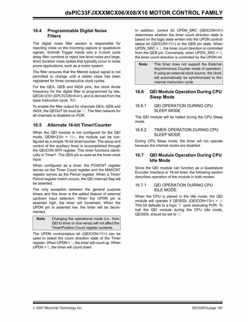
dsPIC33FJXXXMCX06/X08/X10 MOTOR CONTROL FAMILY
16.4 Programmable Digital Noise Filters
The digital noise filter section is responsible forrejecting noise on the incoming capture or quadraturesignals. Schmitt Trigger inputs and a 3-clock cycledelay filter combine to reject low-level noise and large,short duration noise spikes that typically occur in noiseprone applications, such as a motor system.
The filter ensures that the filtered output signal is notpermitted to change until a stable value has beenregistered for three consecutive clock cycles.
For the QEA, QEB and INDX pins, the clock dividefrequency for the digital filter is programmed by bits,QECK<2:0> (DFLTCON<6:4>), and is derived from thebase instruction cycle, TCY.
To enable the filter output for channels QEA, QEB andINDX, the QEOUT bit must be ‘1’. The filter network forall channels is disabled on POR.
16.5 Alternate 16-bit Timer/CounterWhen the QEI module is not configured for the QEImode, QEIM<2:0> = 001, the module can be con-figured as a simple 16-bit timer/counter. The setup andcontrol of the auxiliary timer is accomplished throughthe QEICON SFR register. This timer functions identi-cally to Timer1. The QEA pin is used as the timer clockinput.
When configured as a timer, the POSCNT registerserves as the Timer Count register and the MAXCNTregister serves as the Period register. When a Timer/Period register match occurs, the QEI interrupt flag willbe asserted.
The only exception between the general purposetimers and this timer is the added feature of externalup/down input selection. When the UPDN pin isasserted high, the timer will increment. When theUPDN pin is asserted low, the timer will be decre-mented.
The UPDN control/status bit (QEICON<11>) can beused to select the count direction state of the Timerregister. When UPDN = 1, the timer will count up. WhenUPDN = 0, the timer will count down.
In addition, control bit UPDN_SRC (QEICON<0>)determines whether the timer count direction state isbased on the logic state written into the UPDN control/status bit (QEICON<11>) or the QEB pin state. WhenUPDN_SRC = 1, the timer count direction is controlledfrom the QEB pin. Conversely, when UPDN_SRC = 0,the timer count direction is controlled by the UPDN bit.
16.6 QEI Module Operation During CPU Sleep Mode
16.6.1 QEI OPERATION DURING CPU SLEEP MODE
The QEI module will be halted during the CPU Sleepmode.
16.6.2 TIMER OPERATION DURING CPU SLEEP MODE
During CPU Sleep mode, the timer will not operatebecause the internal clocks are disabled.
16.7 QEI Module Operation During CPU Idle Mode
Since the QEI module can function as a QuadratureEncoder Interface or 16-bit timer, the following sectiondescribes operation of the module in both modes.
16.7.1 QEI OPERATION DURING CPU IDLE MODE
When the CPU is placed in the Idle mode, the QEImodule will operate if QEISIDL (QEICON<13>) = 0.This bit defaults to a logic ‘0’ upon executing POR. Tohalt the QEI module during the CPU Idle mode,QEISIDL should be set to ‘1’.
Note: Changing the operational mode (i.e., fromQEI to timer or vice versa) will not affect theTimer/Position Count register contents.
Note: This timer does not support the ExternalAsynchronous Counter mode of operation.If using an external clock source, the clockwill automatically be synchronized to theinternal instruction cycle.
© 2007 Microchip Technology Inc. DS70287A-page 187
dsPIC33FJXXXMCX06/X08/X10 MOTOR CONTROL FAMILY
16.7.2 TIMER OPERATION DURING CPU IDLE MODE
When the CPU is placed in the Idle mode and the QEImodule is configured in the 16-bit Timer mode, the16-bit timer will operate if QEISIDL (QEICON<13>) = 0.This bit defaults to a logic ‘0’ upon executing POR. Tohalt the timer module during the CPU Idle mode,QEISIDL should be set to ‘1’.
If the QEISIDL bit is cleared, the timer will functionnormally – as if the CPU Idle mode had not beenentered.
16.8 Quadrature Encoder Interface Interrupts
The Quadrature Encoder Interface has the ability togenerate an interrupt on the occurrence of the followingevents:
• Interrupt on 16-bit up/down position counter rollover/underflow
• Detection of qualified index pulse or if CNTERR bit is set
• Timer period match event (overflow/underflow)• Gate accumulation event
The QEI Interrupt Flag bit, QEIIF, is asserted uponoccurrence of any of the above events. The QEIIF bitmust be cleared in software. QEIIF is located in theIFS3 register.
Enabling an interrupt is accomplished via the respec-tive enable bit, QEIIE. The QEIIE bit is located in theIEC3 register.
16.9 Control and Status RegistersThe QEI module has four user-accessible registers.The registers are accessible in either Byte or Wordmode. These registers are as follows:
• Control/Status Register (QEICON) – This register allows control of the QEI operation and status flags indicating the module’s state.
• Digital Filter Control Register (DFLTCON) – This register allows control of the digital input filter operation.
• Position Count Register (POSCNT) – This regis-ter allows reading and writing of the 16-bit position counter.
• Maximum Count Register (MAXCNT) – The MAXCNT register holds a value that is compared to the POSCNT counter in some operations.
Note: The POSCNT register allows byteaccesses; however, reading the register inbyte mode may result in partially updatedvalues in subsequent reads. Either useWord mode reads/writes or ensure thatthe counter is not counting during byteoperations.
DS70287A-page 188 © 2007 Microchip Technology Inc.
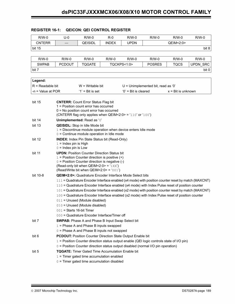
dsPIC33FJXXXMCX06/X08/X10 MOTOR CONTROL FAMILY
REGISTER 16-1: QEICON: QEI CONTROL REGISTER
R/W-0 U-0 R/W-0 R-0 R/W-0 R/W-0 R/W-0 R/W-0CNTERR — QEISIDL INDEX UPDN QEIM<2:0>
bit 15 bit 8
R/W-0 R/W-0 R/W-0 R/W-0 R/W-0 R/W-0 R/W-0 R/W-0SWPAB PCDOUT TQGATE TQCKPS<1:0> POSRES TQCS UPDN_SRC
bit 7 bit 0
Legend:R = Readable bit W = Writable bit U = Unimplemented bit, read as ‘0’-n = Value at POR ‘1’ = Bit is set ‘0’ = Bit is cleared x = Bit is unknown
bit 15 CNTERR: Count Error Status Flag bit1 = Position count error has occurred0 = No position count error has occurred(CNTERR flag only applies when QEIM<2:0> = ‘110’ or ‘100’)
bit 14 Unimplemented: Read as ‘0’bit 13 QEISIDL: Stop in Idle Mode bit
1 = Discontinue module operation when device enters Idle mode0 = Continue module operation in Idle mode
bit 12 INDEX: Index Pin State Status bit (Read-Only)1 = Index pin is High0 = Index pin is Low
bit 11 UPDN: Position Counter Direction Status bit1 = Position Counter direction is positive (+)0 = Position Counter direction is negative (-)(Read-only bit when QEIM<2:0> = ‘1XX’)(Read/Write bit when QEIM<2:0> = ‘001’)
bit 10-8 QEIM<2:0>: Quadrature Encoder Interface Mode Select bits111 = Quadrature Encoder Interface enabled (x4 mode) with position counter reset by match (MAXCNT)110 = Quadrature Encoder Interface enabled (x4 mode) with Index Pulse reset of position counter101 = Quadrature Encoder Interface enabled (x2 mode) with position counter reset by match (MAXCNT)100 = Quadrature Encoder Interface enabled (x2 mode) with Index Pulse reset of position counter011 = Unused (Module disabled)010 = Unused (Module disabled)001 = Starts 16-bit Timer000 = Quadrature Encoder Interface/Timer off
bit 7 SWPAB: Phase A and Phase B Input Swap Select bit1 = Phase A and Phase B inputs swapped0 = Phase A and Phase B inputs not swapped
bit 6 PCDOUT: Position Counter Direction State Output Enable bit1 = Position Counter direction status output enable (QEI logic controls state of I/O pin)0 = Position Counter direction status output disabled (normal I/O pin operation)
bit 5 TQGATE: Timer Gated Time Accumulation Enable bit1 = Timer gated time accumulation enabled0 = Timer gated time accumulation disabled
© 2007 Microchip Technology Inc. DS70287A-page 189
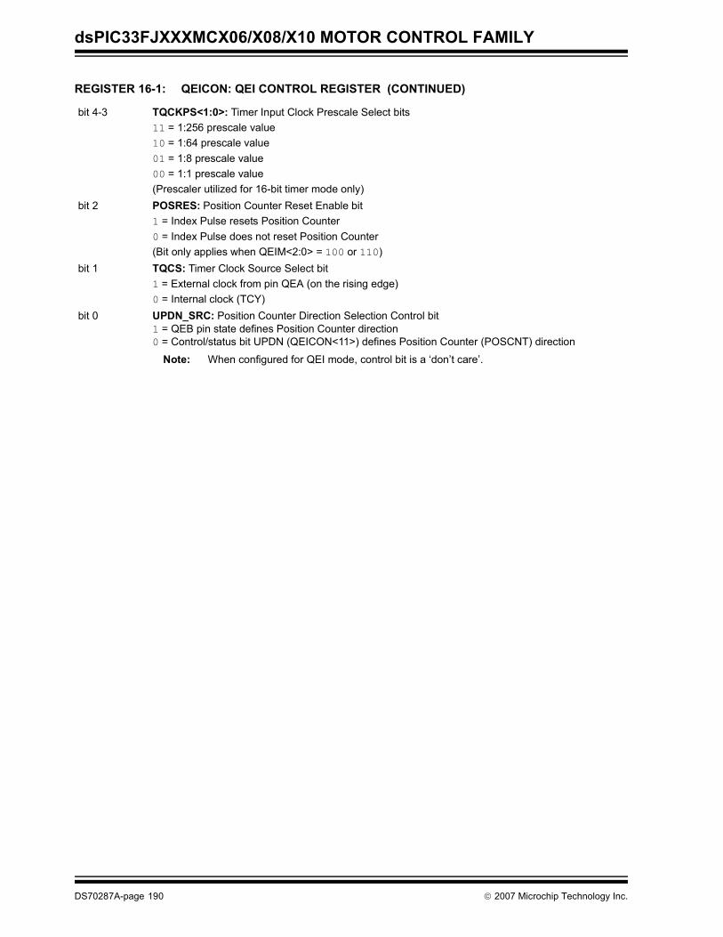
dsPIC33FJXXXMCX06/X08/X10 MOTOR CONTROL FAMILY
bit 4-3 TQCKPS<1:0>: Timer Input Clock Prescale Select bits11 = 1:256 prescale value10 = 1:64 prescale value01 = 1:8 prescale value00 = 1:1 prescale value(Prescaler utilized for 16-bit timer mode only)
bit 2 POSRES: Position Counter Reset Enable bit1 = Index Pulse resets Position Counter0 = Index Pulse does not reset Position Counter(Bit only applies when QEIM<2:0> = 100 or 110)
bit 1 TQCS: Timer Clock Source Select bit1 = External clock from pin QEA (on the rising edge)0 = Internal clock (TCY)
bit 0 UPDN_SRC: Position Counter Direction Selection Control bit1 = QEB pin state defines Position Counter direction0 = Control/status bit UPDN (QEICON<11>) defines Position Counter (POSCNT) direction
Note: When configured for QEI mode, control bit is a ‘don’t care’.
REGISTER 16-1: QEICON: QEI CONTROL REGISTER (CONTINUED)
DS70287A-page 190 © 2007 Microchip Technology Inc.
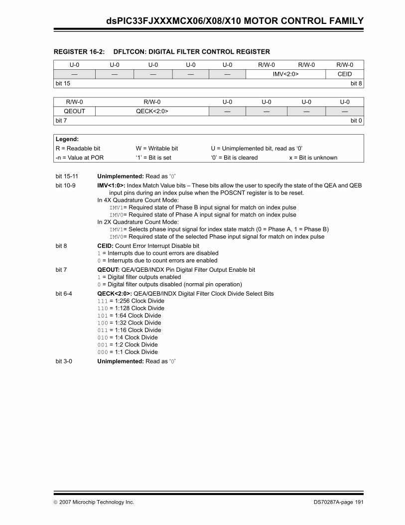
dsPIC33FJXXXMCX06/X08/X10 MOTOR CONTROL FAMILY
REGISTER 16-2: DFLTCON: DIGITAL FILTER CONTROL REGISTER
U-0 U-0 U-0 U-0 U-0 R/W-0 R/W-0 R/W-0— — — — — IMV<2:0> CEID
bit 15 bit 8
R/W-0 R/W-0 U-0 U-0 U-0 U-0QEOUT QECK<2:0> — — — —
bit 7 bit 0
Legend:R = Readable bit W = Writable bit U = Unimplemented bit, read as ‘0’-n = Value at POR ‘1’ = Bit is set ‘0’ = Bit is cleared x = Bit is unknown
bit 15-11 Unimplemented: Read as ‘0’bit 10-9 IMV<1:0>: Index Match Value bits – These bits allow the user to specify the state of the QEA and QEB
input pins during an index pulse when the POSCNT register is to be reset.In 4X Quadrature Count Mode:
IMV1= Required state of Phase B input signal for match on index pulseIMV0= Required state of Phase A input signal for match on index pulse
In 2X Quadrature Count Mode:IMV1= Selects phase input signal for index state match (0 = Phase A, 1 = Phase B)IMV0= Required state of the selected Phase input signal for match on index pulse
bit 8 CEID: Count Error Interrupt Disable bit1 = Interrupts due to count errors are disabled0 = Interrupts due to count errors are enabled
bit 7 QEOUT: QEA/QEB/INDX Pin Digital Filter Output Enable bit1 = Digital filter outputs enabled0 = Digital filter outputs disabled (normal pin operation)
bit 6-4 QECK<2:0>: QEA/QEB/INDX Digital Filter Clock Divide Select Bits111 = 1:256 Clock Divide110 = 1:128 Clock Divide101 = 1:64 Clock Divide100 = 1:32 Clock Divide011 = 1:16 Clock Divide010 = 1:4 Clock Divide001 = 1:2 Clock Divide000 = 1:1 Clock Divide
bit 3-0 Unimplemented: Read as ‘0’
© 2007 Microchip Technology Inc. DS70287A-page 191

dsPIC33FJXXXMCX06/X08/X10 MOTOR CONTROL FAMILY
NOTES:
DS70287A-page 192 © 2007 Microchip Technology Inc.
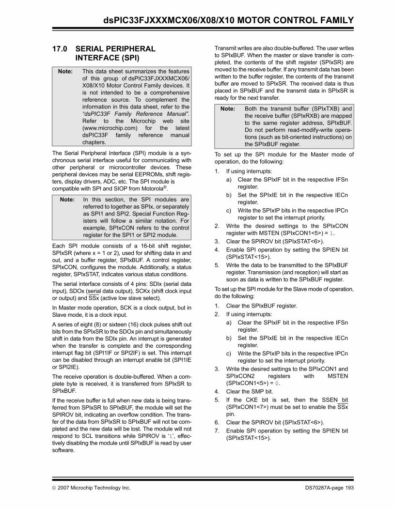
dsPIC33FJXXXMCX06/X08/X10 MOTOR CONTROL FAMILY
17.0 SERIAL PERIPHERAL INTERFACE (SPI)
The Serial Peripheral Interface (SPI) module is a syn-chronous serial interface useful for communicating withother peripheral or microcontroller devices. Theseperipheral devices may be serial EEPROMs, shift regis-ters, display drivers, ADC, etc. The SPI module is compatible with SPI and SIOP from Motorola®.
Each SPI module consists of a 16-bit shift register,SPIxSR (where x = 1 or 2), used for shifting data in andout, and a buffer register, SPIxBUF. A control register,SPIxCON, configures the module. Additionally, a statusregister, SPIxSTAT, indicates various status conditions.
The serial interface consists of 4 pins: SDIx (serial datainput), SDOx (serial data output), SCKx (shift clock inputor output) and SSx (active low slave select).
In Master mode operation, SCK is a clock output, but inSlave mode, it is a clock input.
A series of eight (8) or sixteen (16) clock pulses shift outbits from the SPIxSR to the SDOx pin and simultaneouslyshift in data from the SDIx pin. An interrupt is generatedwhen the transfer is complete and the correspondinginterrupt flag bit (SPI1IF or SPI2IF) is set. This interruptcan be disabled through an interrupt enable bit (SPI1IEor SPI2IE).
The receive operation is double-buffered. When a com-plete byte is received, it is transferred from SPIxSR toSPIxBUF.
If the receive buffer is full when new data is being trans-ferred from SPIxSR to SPIxBUF, the module will set theSPIROV bit, indicating an overflow condition. The trans-fer of the data from SPIxSR to SPIxBUF will not be com-pleted and the new data will be lost. The module will notrespond to SCL transitions while SPIROV is ‘1’, effec-tively disabling the module until SPIxBUF is read by usersoftware.
Transmit writes are also double-buffered. The user writesto SPIxBUF. When the master or slave transfer is com-pleted, the contents of the shift register (SPIxSR) aremoved to the receive buffer. If any transmit data has beenwritten to the buffer register, the contents of the transmitbuffer are moved to SPIxSR. The received data is thusplaced in SPIxBUF and the transmit data in SPIxSR isready for the next transfer.
To set up the SPI module for the Master mode ofoperation, do the following:
1. If using interrupts:a) Clear the SPIxIF bit in the respective IFSn
register.b) Set the SPIxIE bit in the respective IECn
register.c) Write the SPIxIP bits in the respective IPCn
register to set the interrupt priority.2. Write the desired settings to the SPIxCON
register with MSTEN (SPIxCON1<5>) = 1. 3. Clear the SPIROV bit (SPIxSTAT<6>).4. Enable SPI operation by setting the SPIEN bit
(SPIxSTAT<15>).5. Write the data to be transmitted to the SPIxBUF
register. Transmission (and reception) will start assoon as data is written to the SPIxBUF register.
To set up the SPI module for the Slave mode of operation,do the following:
1. Clear the SPIxBUF register.2. If using interrupts:
a) Clear the SPIxIF bit in the respective IFSnregister.
b) Set the SPIxIE bit in the respective IECnregister.
c) Write the SPIxIP bits in the respective IPCnregister to set the interrupt priority.
3. Write the desired settings to the SPIxCON1 andSPIxCON2 registers with MSTEN(SPIxCON1<5>) = 0.
4. Clear the SMP bit.5. If the CKE bit is set, then the SSEN bit
(SPIxCON1<7>) must be set to enable the SSxpin.
6. Clear the SPIROV bit (SPIxSTAT<6>).7. Enable SPI operation by setting the SPIEN bit
(SPIxSTAT<15>).
Note: This data sheet summarizes the featuresof this group of dsPIC33FJXXXMCX06/X08/X10 Motor Control Family devices. Itis not intended to be a comprehensivereference source. To complement theinformation in this data sheet, refer to the“dsPIC33F Family Reference Manual”.Refer to the Microchip web site(www.microchip.com) for the latestdsPIC33F family reference manualchapters.
Note: In this section, the SPI modules arereferred to together as SPIx, or separatelyas SPI1 and SPI2. Special Function Reg-isters will follow a similar notation. Forexample, SPIxCON refers to the controlregister for the SPI1 or SPI2 module.
Note: Both the transmit buffer (SPIxTXB) andthe receive buffer (SPIxRXB) are mappedto the same register address, SPIxBUF.Do not perform read-modify-write opera-tions (such as bit-oriented instructions) onthe SPIxBUF register.
© 2007 Microchip Technology Inc. DS70287A-page 193
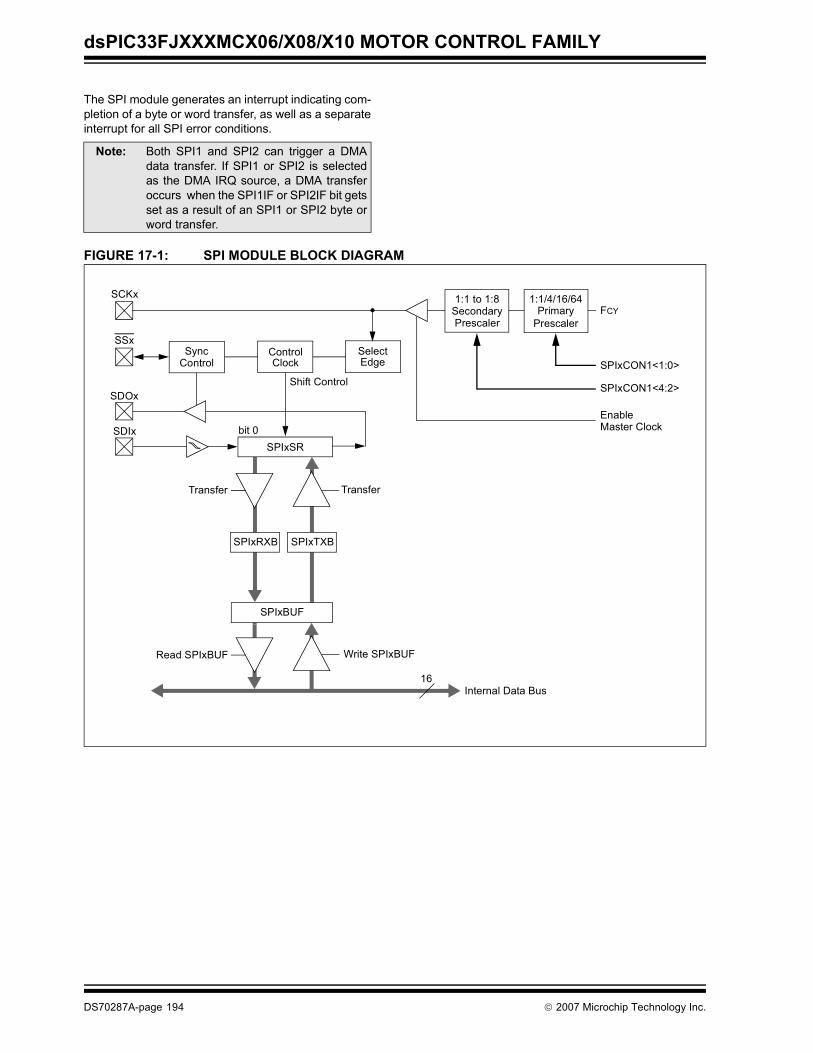
dsPIC33FJXXXMCX06/X08/X10 MOTOR CONTROL FAMILY
The SPI module generates an interrupt indicating com-pletion of a byte or word transfer, as well as a separateinterrupt for all SPI error conditions.
FIGURE 17-1: SPI MODULE BLOCK DIAGRAM
Note: Both SPI1 and SPI2 can trigger a DMAdata transfer. If SPI1 or SPI2 is selectedas the DMA IRQ source, a DMA transferoccurs when the SPI1IF or SPI2IF bit getsset as a result of an SPI1 or SPI2 byte orword transfer.
Internal Data Bus
SDIx
SDOx
SSx
SCKx
SPIxSRbit 0
Shift Control
EdgeSelect
FCYPrimary1:1/4/16/64
Enable
Prescaler
Sync
SPIxBUF
Control
TransferTransfer
Write SPIxBUFRead SPIxBUF
16
SPIxCON1<1:0>
SPIxCON1<4:2>
Master Clock
ClockControl
SecondaryPrescaler
1:1 to 1:8
SPIxRXB SPIxTXB
DS70287A-page 194 © 2007 Microchip Technology Inc.
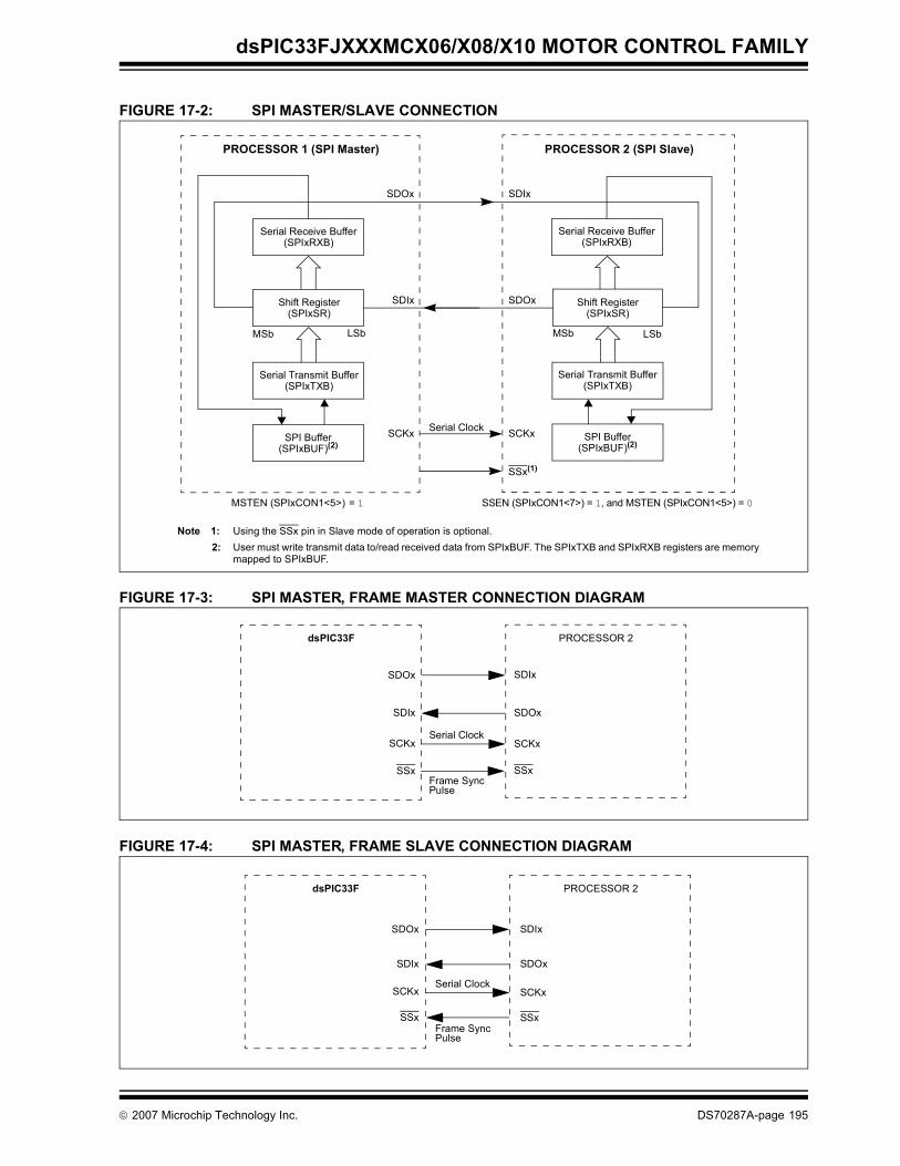
dsPIC33FJXXXMCX06/X08/X10 MOTOR CONTROL FAMILY
FIGURE 17-2: SPI MASTER/SLAVE CONNECTION
FIGURE 17-3: SPI MASTER, FRAME MASTER CONNECTION DIAGRAM
FIGURE 17-4: SPI MASTER, FRAME SLAVE CONNECTION DIAGRAM
Serial Receive Buffer(SPIxRXB)
LSbMSb
SDIx
SDOx
PROCESSOR 2 (SPI Slave)
SCKx
SSx(1)
Serial Transmit Buffer(SPIxTXB)
Serial Receive Buffer(SPIxRXB)
Shift Register(SPIxSR)
MSb LSb
SDOx
SDIx
PROCESSOR 1 (SPI Master)
Serial Clock
SSEN (SPIxCON1<7>) = 1, and MSTEN (SPIxCON1<5>) = 0
Note 1: Using the SSx pin in Slave mode of operation is optional.2: User must write transmit data to/read received data from SPIxBUF. The SPIxTXB and SPIxRXB registers are memory
mapped to SPIxBUF.
SCKx
Serial Transmit Buffer(SPIxTXB)
MSTEN (SPIxCON1<5>) = 1
SPI Buffer(SPIxBUF)(2)
SPI Buffer(SPIxBUF)(2)
Shift Register(SPIxSR)
SDOx
SDIx
dsPIC33F
Serial Clock
SSx
SCKx
Frame SyncPulse
SDIx
SDOx
PROCESSOR 2
SSx
SCKx
SDOx
SDIx
dsPIC33F
Serial Clock
SSx
SCKx
Frame SyncPulse
SDIx
SDOx
PROCESSOR 2
SSx
SCKx
© 2007 Microchip Technology Inc. DS70287A-page 195
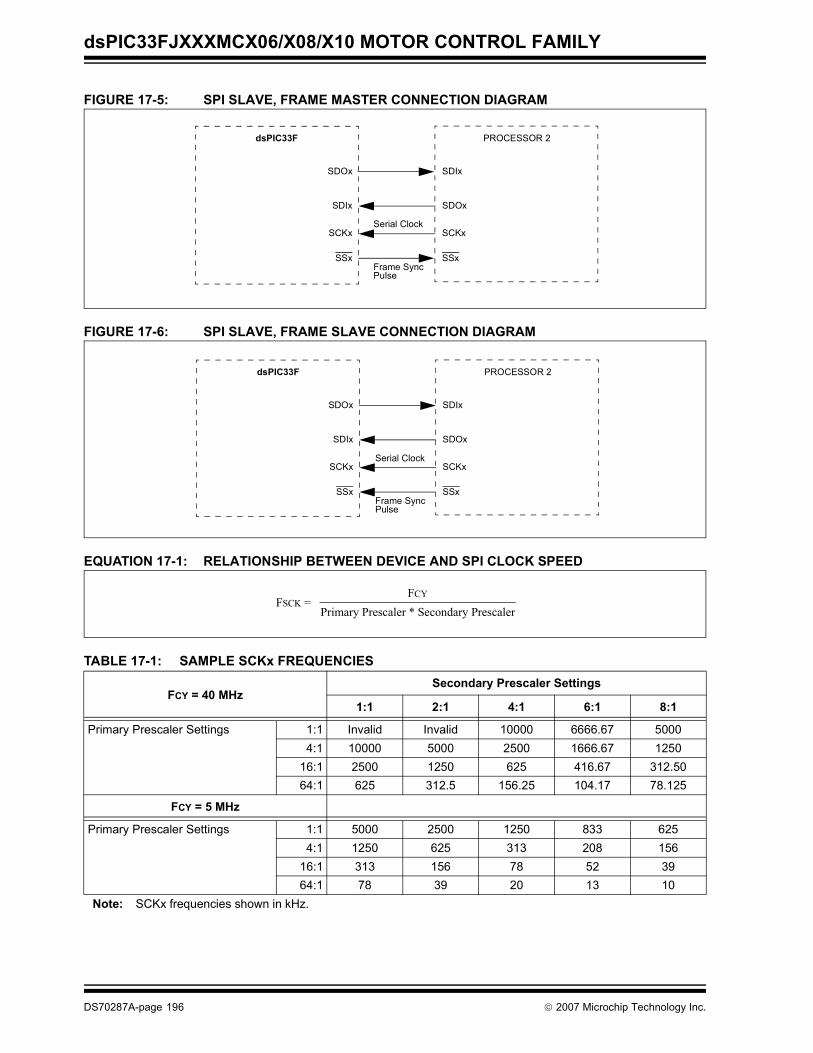
dsPIC33FJXXXMCX06/X08/X10 MOTOR CONTROL FAMILY
FIGURE 17-5: SPI SLAVE, FRAME MASTER CONNECTION DIAGRAM
FIGURE 17-6: SPI SLAVE, FRAME SLAVE CONNECTION DIAGRAM
EQUATION 17-1: RELATIONSHIP BETWEEN DEVICE AND SPI CLOCK SPEED
TABLE 17-1: SAMPLE SCKx FREQUENCIES
FCY = 40 MHzSecondary Prescaler Settings
1:1 2:1 4:1 6:1 8:1
Primary Prescaler Settings 1:1 Invalid Invalid 10000 6666.67 50004:1 10000 5000 2500 1666.67 1250
16:1 2500 1250 625 416.67 312.5064:1 625 312.5 156.25 104.17 78.125
FCY = 5 MHz
Primary Prescaler Settings 1:1 5000 2500 1250 833 6254:1 1250 625 313 208 156
16:1 313 156 78 52 3964:1 78 39 20 13 10
Note: SCKx frequencies shown in kHz.
SDOx
SDIx
dsPIC33F
Serial Clock
SSx
SCKx
Frame SyncPulse
SDIx
SDOx
PROCESSOR 2
SSx
SCKx
SDOx
SDIx
dsPIC33F
Serial Clock
SSx
SCKx
Frame SyncPulse
SDIx
SDOx
PROCESSOR 2
SSx
SCKx
Primary Prescaler * Secondary PrescalerFCY
FSCK =
DS70287A-page 196 © 2007 Microchip Technology Inc.
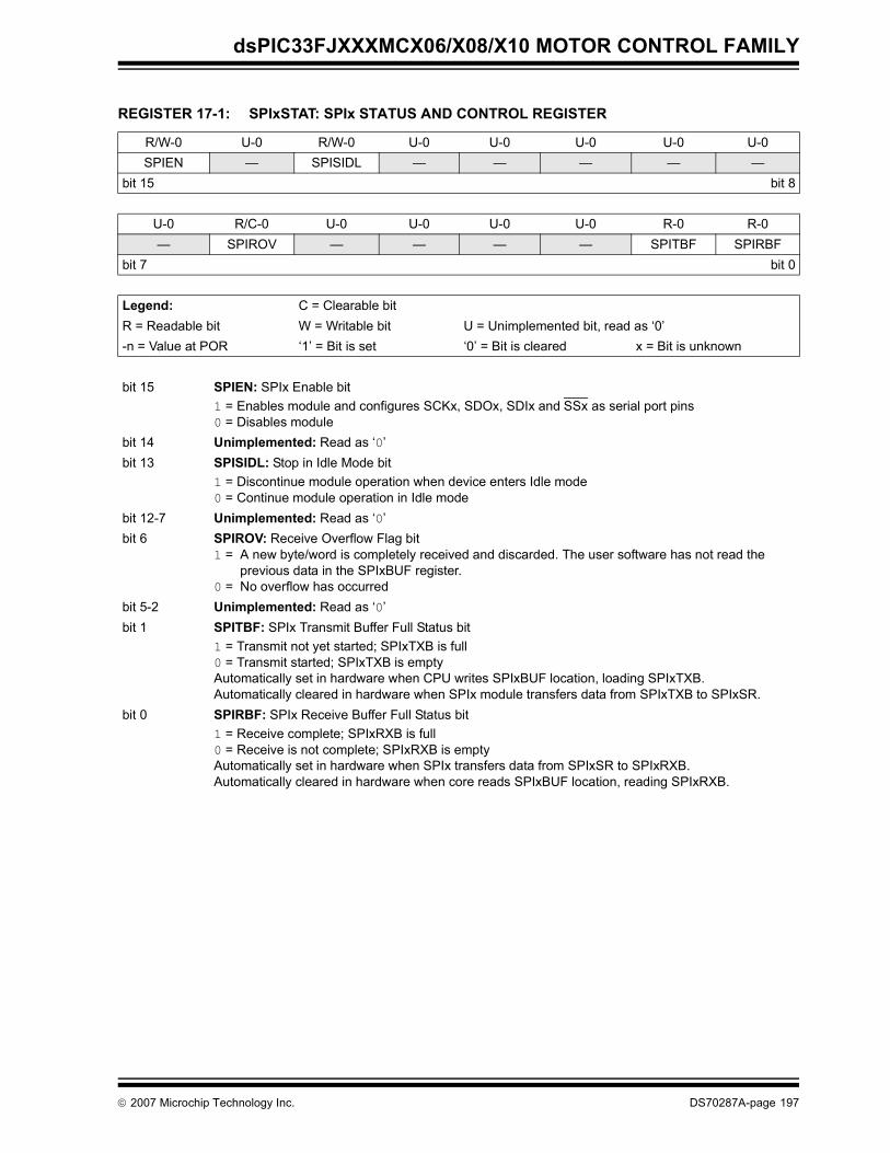
dsPIC33FJXXXMCX06/X08/X10 MOTOR CONTROL FAMILY
REGISTER 17-1: SPIxSTAT: SPIx STATUS AND CONTROL REGISTER
R/W-0 U-0 R/W-0 U-0 U-0 U-0 U-0 U-0SPIEN — SPISIDL — — — — —
bit 15 bit 8
U-0 R/C-0 U-0 U-0 U-0 U-0 R-0 R-0— SPIROV — — — — SPITBF SPIRBF
bit 7 bit 0
Legend: C = Clearable bitR = Readable bit W = Writable bit U = Unimplemented bit, read as ‘0’-n = Value at POR ‘1’ = Bit is set ‘0’ = Bit is cleared x = Bit is unknown
bit 15 SPIEN: SPIx Enable bit1 = Enables module and configures SCKx, SDOx, SDIx and SSx as serial port pins0 = Disables module
bit 14 Unimplemented: Read as ‘0’bit 13 SPISIDL: Stop in Idle Mode bit
1 = Discontinue module operation when device enters Idle mode0 = Continue module operation in Idle mode
bit 12-7 Unimplemented: Read as ‘0’bit 6 SPIROV: Receive Overflow Flag bit
1 = A new byte/word is completely received and discarded. The user software has not read the previous data in the SPIxBUF register.
0 = No overflow has occurredbit 5-2 Unimplemented: Read as ‘0’bit 1 SPITBF: SPIx Transmit Buffer Full Status bit
1 = Transmit not yet started; SPIxTXB is full0 = Transmit started; SPIxTXB is emptyAutomatically set in hardware when CPU writes SPIxBUF location, loading SPIxTXB.Automatically cleared in hardware when SPIx module transfers data from SPIxTXB to SPIxSR.
bit 0 SPIRBF: SPIx Receive Buffer Full Status bit1 = Receive complete; SPIxRXB is full0 = Receive is not complete; SPIxRXB is emptyAutomatically set in hardware when SPIx transfers data from SPIxSR to SPIxRXB.Automatically cleared in hardware when core reads SPIxBUF location, reading SPIxRXB.
© 2007 Microchip Technology Inc. DS70287A-page 197
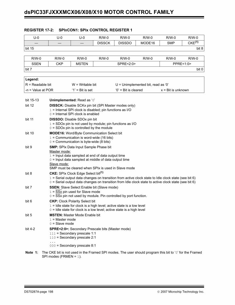
dsPIC33FJXXXMCX06/X08/X10 MOTOR CONTROL FAMILY
REGISTER 17-2: SPIXCON1: SPIx CONTROL REGISTER 1
U-0 U-0 U-0 R/W-0 R/W-0 R/W-0 R/W-0 R/W-0— — — DISSCK DISSDO MODE16 SMP CKE(1)
bit 15 bit 8
R/W-0 R/W-0 R/W-0 R/W-0 R/W-0 R/W-0 R/W-0 R/W-0SSEN CKP MSTEN SPRE<2:0> PPRE<1:0>
bit 7 bit 0
Legend:R = Readable bit W = Writable bit U = Unimplemented bit, read as ‘0’-n = Value at POR ‘1’ = Bit is set ‘0’ = Bit is cleared x = Bit is unknown
bit 15-13 Unimplemented: Read as ‘0’bit 12 DISSCK: Disable SCKx pin bit (SPI Master modes only)
1 = Internal SPI clock is disabled; pin functions as I/O0 = Internal SPI clock is enabled
bit 11 DISSDO: Disable SDOx pin bit1 = SDOx pin is not used by module; pin functions as I/O0 = SDOx pin is controlled by the module
bit 10 MODE16: Word/Byte Communication Select bit1 = Communication is word-wide (16 bits)0 = Communication is byte-wide (8 bits)
bit 9 SMP: SPIx Data Input Sample Phase bitMaster mode:1 = Input data sampled at end of data output time0 = Input data sampled at middle of data output timeSlave mode:SMP must be cleared when SPIx is used in Slave mode
bit 8 CKE: SPIx Clock Edge Select bit(1)
1 = Serial output data changes on transition from active clock state to Idle clock state (see bit 6)0 = Serial output data changes on transition from Idle clock state to active clock state (see bit 6)
bit 7 SSEN: Slave Select Enable bit (Slave mode)1 = SSx pin used for Slave mode0 = SSx pin not used by module. Pin controlled by port function.
bit 6 CKP: Clock Polarity Select bit1 = Idle state for clock is a high level; active state is a low level0 = Idle state for clock is a low level; active state is a high level
bit 5 MSTEN: Master Mode Enable bit1 = Master mode0 = Slave mode
bit 4-2 SPRE<2:0>: Secondary Prescale bits (Master mode)111 = Secondary prescale 1:1110 = Secondary prescale 2:1...000 = Secondary prescale 8:1
Note 1: The CKE bit is not used in the Framed SPI modes. The user should program this bit to ‘0’ for the Framed SPI modes (FRMEN = 1).
DS70287A-page 198 © 2007 Microchip Technology Inc.
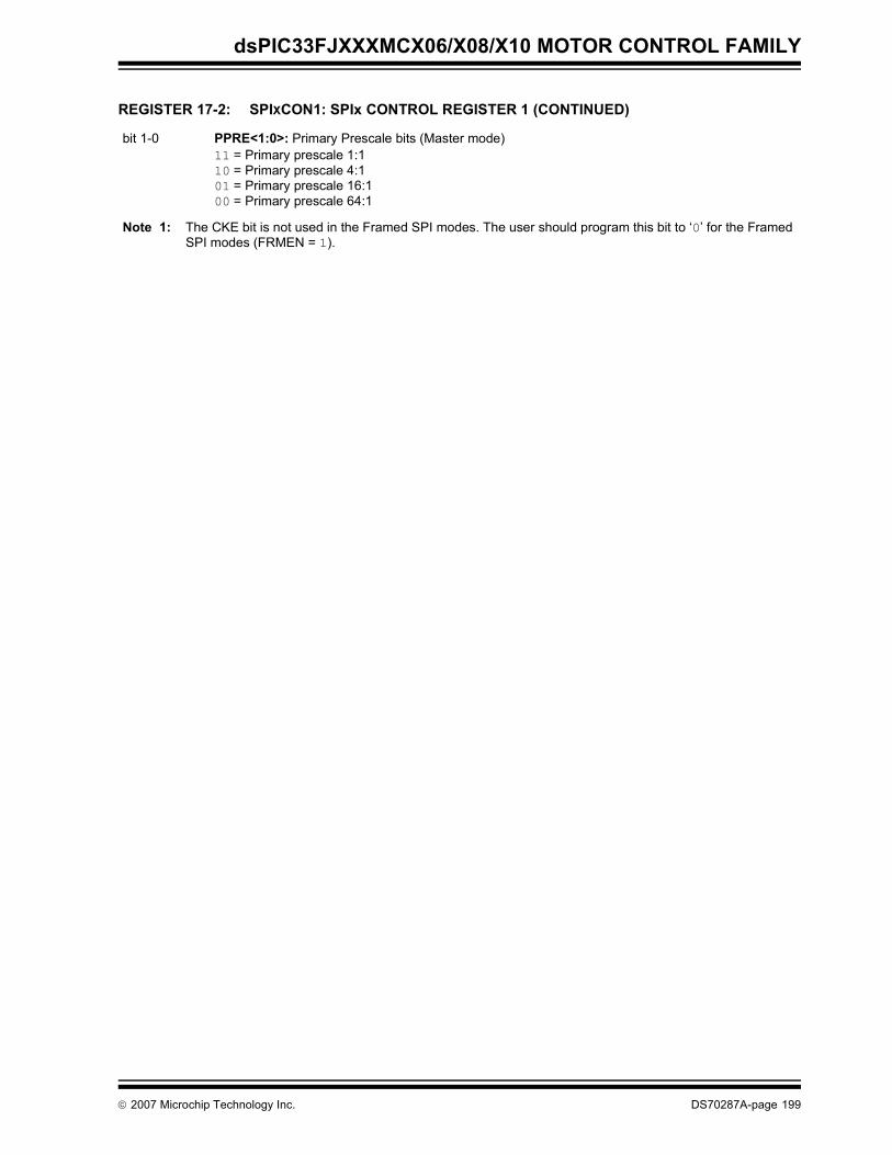
dsPIC33FJXXXMCX06/X08/X10 MOTOR CONTROL FAMILY
bit 1-0 PPRE<1:0>: Primary Prescale bits (Master mode)11 = Primary prescale 1:110 = Primary prescale 4:101 = Primary prescale 16:100 = Primary prescale 64:1
REGISTER 17-2: SPIXCON1: SPIx CONTROL REGISTER 1 (CONTINUED)
Note 1: The CKE bit is not used in the Framed SPI modes. The user should program this bit to ‘0’ for the Framed SPI modes (FRMEN = 1).
© 2007 Microchip Technology Inc. DS70287A-page 199
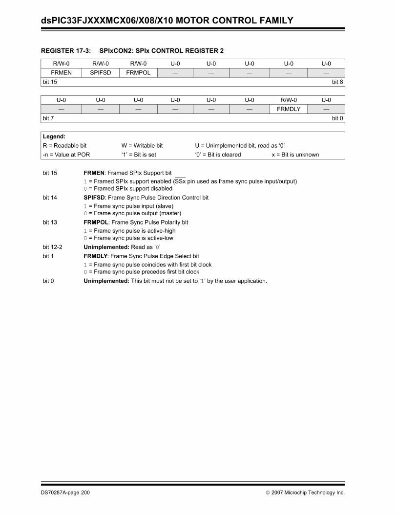
dsPIC33FJXXXMCX06/X08/X10 MOTOR CONTROL FAMILY
REGISTER 17-3: SPIxCON2: SPIx CONTROL REGISTER 2
R/W-0 R/W-0 R/W-0 U-0 U-0 U-0 U-0 U-0FRMEN SPIFSD FRMPOL — — — — —
bit 15 bit 8
U-0 U-0 U-0 U-0 U-0 U-0 R/W-0 U-0— — — — — — FRMDLY —
bit 7 bit 0
Legend:R = Readable bit W = Writable bit U = Unimplemented bit, read as ‘0’-n = Value at POR ‘1’ = Bit is set ‘0’ = Bit is cleared x = Bit is unknown
bit 15 FRMEN: Framed SPIx Support bit1 = Framed SPIx support enabled (SSx pin used as frame sync pulse input/output)0 = Framed SPIx support disabled
bit 14 SPIFSD: Frame Sync Pulse Direction Control bit1 = Frame sync pulse input (slave)0 = Frame sync pulse output (master)
bit 13 FRMPOL: Frame Sync Pulse Polarity bit1 = Frame sync pulse is active-high0 = Frame sync pulse is active-low
bit 12-2 Unimplemented: Read as ‘0’bit 1 FRMDLY: Frame Sync Pulse Edge Select bit
1 = Frame sync pulse coincides with first bit clock0 = Frame sync pulse precedes first bit clock
bit 0 Unimplemented: This bit must not be set to ‘1’ by the user application.
DS70287A-page 200 © 2007 Microchip Technology Inc.
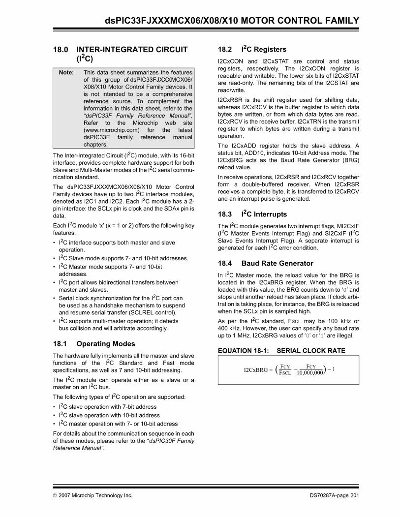
dsPIC33FJXXXMCX06/X08/X10 MOTOR CONTROL FAMILY
18.0 INTER-INTEGRATED CIRCUIT (I2C)
The Inter-Integrated Circuit (I2C) module, with its 16-bitinterface, provides complete hardware support for bothSlave and Multi-Master modes of the I2C serial commu-nication standard.
The dsPIC33FJXXXMCX06/X08/X10 Motor ControlFamily devices have up to two I2C interface modules,denoted as I2C1 and I2C2. Each I2C module has a 2-pin interface: the SCLx pin is clock and the SDAx pin isdata.
Each I2C module ‘x’ (x = 1 or 2) offers the following keyfeatures:
• I2C interface supports both master and slave operation.
• I2C Slave mode supports 7- and 10-bit addresses.• I2C Master mode supports 7- and 10-bit
addresses.• I2C port allows bidirectional transfers between
master and slaves.• Serial clock synchronization for the I2C port can
be used as a handshake mechanism to suspend and resume serial transfer (SCLREL control).
• I2C supports multi-master operation; it detects bus collision and will arbitrate accordingly.
18.1 Operating ModesThe hardware fully implements all the master and slavefunctions of the I2C Standard and Fast modespecifications, as well as 7 and 10-bit addressing.
The I2C module can operate either as a slave or amaster on an I2C bus.
The following types of I2C operation are supported:
• I2C slave operation with 7-bit address• I2C slave operation with 10-bit address• I2C master operation with 7- or 10-bit address
For details about the communication sequence in eachof these modes, please refer to the “dsPIC30F FamilyReference Manual”.
18.2 I2C RegistersI2CxCON and I2CxSTAT are control and statusregisters, respectively. The I2CxCON register isreadable and writable. The lower six bits of I2CxSTATare read-only. The remaining bits of the I2CSTAT areread/write.
I2CxRSR is the shift register used for shifting data,whereas I2CxRCV is the buffer register to which databytes are written, or from which data bytes are read.I2CxRCV is the receive buffer. I2CxTRN is the transmitregister to which bytes are written during a transmitoperation.
The I2CxADD register holds the slave address. Astatus bit, ADD10, indicates 10-bit Address mode. TheI2CxBRG acts as the Baud Rate Generator (BRG)reload value.
In receive operations, I2CxRSR and I2CxRCV togetherform a double-buffered receiver. When I2CxRSRreceives a complete byte, it is transferred to I2CxRCVand an interrupt pulse is generated.
18.3 I2C InterruptsThe I2C module generates two interrupt flags, MI2CxIF(I2C Master Events Interrupt Flag) and SI2CxIF (I2CSlave Events Interrupt Flag). A separate interrupt isgenerated for each I2C error condition.
18.4 Baud Rate Generator In I2C Master mode, the reload value for the BRG islocated in the I2CxBRG register. When the BRG isloaded with this value, the BRG counts down to ‘0’ andstops until another reload has taken place. If clock arbi-tration is taking place, for instance, the BRG is reloadedwhen the SCLx pin is sampled high.
As per the I2C standard, FSCL may be 100 kHz or400 kHz. However, the user can specify any baud rateup to 1 MHz. I2CxBRG values of ‘0’ or ‘1’ are illegal.
EQUATION 18-1: SERIAL CLOCK RATE
Note: This data sheet summarizes the featuresof this group of dsPIC33FJXXXMCX06/X08/X10 Motor Control Family devices. Itis not intended to be a comprehensivereference source. To complement theinformation in this data sheet, refer to the“dsPIC33F Family Reference Manual”.Refer to the Microchip web site(www.microchip.com) for the latestdsPIC33F family reference manualchapters.
I2CxBRG = FCY FCYFSCL 10,000,000 – 1–( )
© 2007 Microchip Technology Inc. DS70287A-page 201
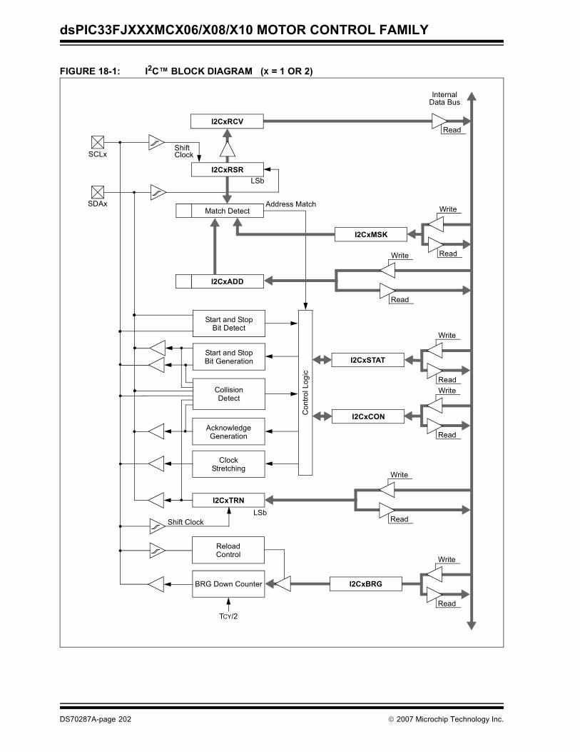
dsPIC33FJXXXMCX06/X08/X10 MOTOR CONTROL FAMILY
FIGURE 18-1: I2C™ BLOCK DIAGRAM (X = 1 OR 2)
InternalData Bus
SCLx
SDAx
Shift
Match Detect
I2CxADD
Start and StopBit Detect
Clock
Address Match
ClockStretching
I2CxTRNLSb
Shift Clock
BRG Down Counter
ReloadControl
TCY/2
Start and StopBit Generation
AcknowledgeGeneration
CollisionDetect
I2CxCON
I2CxSTAT
Con
trol L
ogic
Read
LSb
Write
Read
I2CxBRG
I2CxRSR
Write
Read
Write
Read
Write
Read
Write
Read
Write
Read
I2CxMSK
I2CxRCV
DS70287A-page 202 © 2007 Microchip Technology Inc.
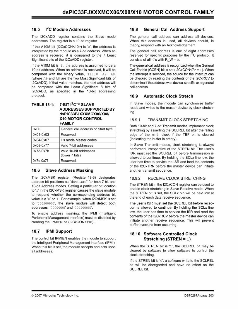
dsPIC33FJXXXMCX06/X08/X10 MOTOR CONTROL FAMILY
18.5 I2C Module AddressesThe I2CxADD register contains the Slave modeaddresses. The register is a 10-bit register.
If the A10M bit (I2CxCON<10>) is ‘0’, the address isinterpreted by the module as a 7-bit address. When anaddress is received, it is compared to the 7 LeastSignificant bits of the I2CxADD register.
If the A10M bit is ‘1’, the address is assumed to be a10-bit address. When an address is received, it will becompared with the binary value, ‘11110 A9 A8’(where A9 and A8 are the two Most Significant bits ofI2CxADD). If that value matches, the next address willbe compared with the Least Significant 8 bits ofI2CxADD, as specified in the 10-bit addressingprotocol.
TABLE 18-1: 7-BIT I2C™ SLAVE ADDRESSES SUPPORTED BY dsPIC33FJXXXMCX06/X08/X10 MOTOR CONTROL FAMILY
18.6 Slave Address MaskingThe I2CxMSK register (Register 18-3) designatesaddress bit positions as “don’t care” for both 7-bit and10-bit Address modes. Setting a particular bit locationto ‘1’ in the I2CxMSK register causes the slave moduleto respond whether the corresponding address bitvalue is a ‘0’ or ‘1’. For example, when I2CxMSK is setto ‘00100000’, the slave module will detect bothaddresses, ‘0000000’ and ‘00100000’.
To enable address masking, the IPMI (IntelligentPeripheral Management Interface) must be disabled byclearing the IPMIEN bit (I2CxCON<11>).
18.7 IPMI SupportThe control bit IPMIEN enables the module to supportthe Intelligent Peripheral Management Interface (IPMI).When this bit is set, the module accepts and acts uponall addresses.
18.8 General Call Address SupportThe general call address can address all devices.When this address is used, all devices should, intheory, respond with an Acknowledgement.
The general call address is one of eight addressesreserved for specific purposes by the I2C protocol. Itconsists of all ‘0’s with R_W = 0.
The general call address is recognized when the GeneralCall Enable (GCEN) bit is set (I2CxCON<7> = 1). Whenthe interrupt is serviced, the source for the interrupt canbe checked by reading the contents of the I2CxRCV todetermine if the address was device-specific or a generalcall address.
18.9 Automatic Clock StretchIn Slave modes, the module can synchronize bufferreads and writes to the master device by clock stretch-ing.
18.9.1 TRANSMIT CLOCK STRETCHINGBoth 10-bit and 7-bit Transmit modes implement clockstretching by asserting the SCLREL bit after the fallingedge of the ninth clock if the TBF bit is cleared(indicating the buffer is empty).
In Slave Transmit modes, clock stretching is alwaysperformed, irrespective of the STREN bit. The user’sISR must set the SCLREL bit before transmission isallowed to continue. By holding the SCLx line low, theuser has time to service the ISR and load the contentsof the I2CxTRN before the master device can initiateanother transmit sequence.
18.9.2 RECEIVE CLOCK STRETCHINGThe STREN bit in the I2CxCON register can be used toenable clock stretching in Slave Receive mode. Whenthe STREN bit is set, the SCLx pin will be held low atthe end of each data receive sequence.
The user’s ISR must set the SCLREL bit before recep-tion is allowed to continue. By holding the SCLx linelow, the user has time to service the ISR and read thecontents of the I2CxRCV before the master device caninitiate another receive sequence. This will preventbuffer overruns from occurring.
18.10 Software Controlled Clock Stretching (STREN = 1)
When the STREN bit is ‘1’, the SCLREL bit may becleared by software to allow software to control theclock stretching.
If the STREN bit is ‘0’, a software write to the SCLRELbit will be disregarded and have no effect on theSCLREL bit.
0x00 General call address or Start byte0x01-0x03 Reserved0x04-0x07 Hs mode Master codes0x08-0x77 Valid 7-bit addresses0x78-0x7b Valid 10-bit addresses
(lower 7 bits)0x7c-0x7f Reserved
© 2007 Microchip Technology Inc. DS70287A-page 203
dsPIC33FJXXXMCX06/X08/X10 MOTOR CONTROL FAMILY
18.11 Slope ControlThe I2C standard requires slope control on the SDAxand SCLx signals for Fast mode (400 kHz). The controlbit DISSLW enables the user to disable slew rate con-trol if desired. It is necessary to disable the slew ratecontrol for 1 MHz mode.
18.12 Clock ArbitrationClock arbitration occurs when the master deasserts theSCLx pin (SCLx allowed to float high) during anyreceive, transmit or Restart/Stop condition. When theSCLx pin is allowed to float high, the Baud Rate Gen-erator (BRG) is suspended from counting until theSCLx pin is actually sampled high. When the SCLx pinis sampled high, the Baud Rate Generator is reloadedwith the contents of I2CxBRG and begins counting.This ensures that the SCLx high time will always be atleast one BRG rollover count in the event that the clockis held low by an external device.
18.13 Multi-Master Communication, Bus Collision and Bus Arbitration
Multi-Master mode support is achieved by busarbitration. When the master outputs address/data bitsonto the SDAx pin, arbitration takes place when themaster outputs a ‘1’ on SDAx by letting SDAx float highwhile another master asserts a ‘0’. When the SCLx pinfloats high, data should be stable. If the expected dataon SDAx is a ‘1’ and the data sampled on theSDAx pin = 0, then a bus collision has taken place. Themaster will set the I2C master events interrupt flag andreset the master portion of the I2C port to its Idle state.
DS70287A-page 204 © 2007 Microchip Technology Inc.
dsPIC33FJXXXMCX06/X08/X10 MOTOR CONTROL FAMILY
REGISTER 18-1: I2CxCON: I2Cx CONTROL REGISTER
R/W-0 U-0 R/W-0 R/W-1 HC R/W-0 R/W-0 R/W-0 R/W-0I2CEN — I2CSIDL SCLREL IPMIEN A10M DISSLW SMEN
bit 15 bit 8
R/W-0 R/W-0 R/W-0 R/W-0 HC R/W-0 HC R/W-0 HC R/W-0 HC R/W-0 HCGCEN STREN ACKDT ACKEN RCEN PEN RSEN SEN
bit 7 bit 0
Legend: U = Unimplemented bit, read as ‘0’R = Readable bit W = Writable bit HS = Set in hardware HC = Cleared in hardware-n = Value at POR ‘1’ = Bit is set ‘0’ = Bit is cleared x = Bit is unknown
bit 15 I2CEN: I2Cx Enable bit 1 = Enables the I2Cx module and configures the SDAx and SCLx pins as serial port pins0 = Disables the I2Cx module. All I2C pins are controlled by port functions.
bit 14 Unimplemented: Read as ‘0’bit 13 I2CSIDL: Stop in Idle Mode bit
1 = Discontinue module operation when device enters an Idle mode0 = Continue module operation in Idle mode
bit 12 SCLREL: SCLx Release Control bit (when operating as I2C slave)1 = Release SCLx clock0 = Hold SCLx clock low (clock stretch)If STREN = 1: Bit is R/W (i.e., software may write ‘0’ to initiate stretch and write ‘1’ to release clock). Hardware clearat beginning of slave transmission. Hardware clear at end of slave reception.If STREN = 0: Bit is R/S (i.e., software may only write ‘1’ to release clock). Hardware clear at beginning of slavetransmission.
bit 11 IPMIEN: Intelligent Peripheral Management Interface (IPMI) Enable bit1 = IPMI mode is enabled; all addresses Acknowledged0 = IPMI mode disabled
bit 10 A10M: 10-bit Slave Address bit1 = I2CxADD is a 10-bit slave address0 = I2CxADD is a 7-bit slave address
bit 9 DISSLW: Disable Slew Rate Control bit1 = Slew rate control disabled0 = Slew rate control enabled
bit 8 SMEN: SMBus Input Levels bit1 = Enable I/O pin thresholds compliant with SMBus specification0 = Disable SMBus input thresholds
bit 7 GCEN: General Call Enable bit (when operating as I2C slave)1 = Enable interrupt when a general call address is received in the I2CxRSR
(module is enabled for reception)0 = General call address disabled
bit 6 STREN: SCLx Clock Stretch Enable bit (when operating as I2C slave)Used in conjunction with SCLREL bit.1 = Enable software or receive clock stretching0 = Disable software or receive clock stretching
© 2007 Microchip Technology Inc. DS70287A-page 205
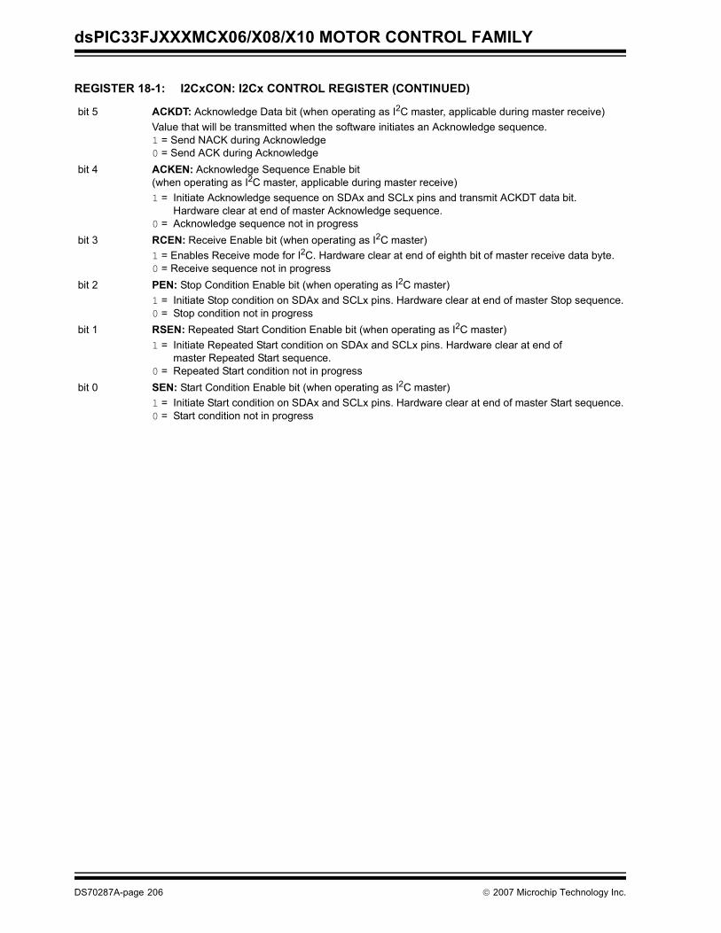
dsPIC33FJXXXMCX06/X08/X10 MOTOR CONTROL FAMILY
bit 5 ACKDT: Acknowledge Data bit (when operating as I2C master, applicable during master receive)Value that will be transmitted when the software initiates an Acknowledge sequence.1 = Send NACK during Acknowledge0 = Send ACK during Acknowledge
bit 4 ACKEN: Acknowledge Sequence Enable bit (when operating as I2C master, applicable during master receive)1 = Initiate Acknowledge sequence on SDAx and SCLx pins and transmit ACKDT data bit.
Hardware clear at end of master Acknowledge sequence.0 = Acknowledge sequence not in progress
bit 3 RCEN: Receive Enable bit (when operating as I2C master)1 = Enables Receive mode for I2C. Hardware clear at end of eighth bit of master receive data byte.0 = Receive sequence not in progress
bit 2 PEN: Stop Condition Enable bit (when operating as I2C master)1 = Initiate Stop condition on SDAx and SCLx pins. Hardware clear at end of master Stop sequence.0 = Stop condition not in progress
bit 1 RSEN: Repeated Start Condition Enable bit (when operating as I2C master)1 = Initiate Repeated Start condition on SDAx and SCLx pins. Hardware clear at end of
master Repeated Start sequence.0 = Repeated Start condition not in progress
bit 0 SEN: Start Condition Enable bit (when operating as I2C master)1 = Initiate Start condition on SDAx and SCLx pins. Hardware clear at end of master Start sequence.0 = Start condition not in progress
REGISTER 18-1: I2CxCON: I2Cx CONTROL REGISTER (CONTINUED)
DS70287A-page 206 © 2007 Microchip Technology Inc.
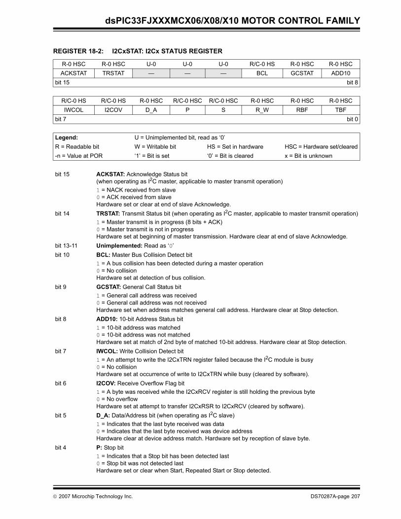
dsPIC33FJXXXMCX06/X08/X10 MOTOR CONTROL FAMILY
REGISTER 18-2: I2CxSTAT: I2Cx STATUS REGISTER
R-0 HSC R-0 HSC U-0 U-0 U-0 R/C-0 HS R-0 HSC R-0 HSCACKSTAT TRSTAT — — — BCL GCSTAT ADD10
bit 15 bit 8
R/C-0 HS R/C-0 HS R-0 HSC R/C-0 HSC R/C-0 HSC R-0 HSC R-0 HSC R-0 HSCIWCOL I2COV D_A P S R_W RBF TBF
bit 7 bit 0
Legend: U = Unimplemented bit, read as ‘0’R = Readable bit W = Writable bit HS = Set in hardware HSC = Hardware set/cleared-n = Value at POR ‘1’ = Bit is set ‘0’ = Bit is cleared x = Bit is unknown
bit 15 ACKSTAT: Acknowledge Status bit (when operating as I2C master, applicable to master transmit operation)1 = NACK received from slave0 = ACK received from slaveHardware set or clear at end of slave Acknowledge.
bit 14 TRSTAT: Transmit Status bit (when operating as I2C master, applicable to master transmit operation)1 = Master transmit is in progress (8 bits + ACK)0 = Master transmit is not in progressHardware set at beginning of master transmission. Hardware clear at end of slave Acknowledge.
bit 13-11 Unimplemented: Read as ‘0’bit 10 BCL: Master Bus Collision Detect bit
1 = A bus collision has been detected during a master operation0 = No collisionHardware set at detection of bus collision.
bit 9 GCSTAT: General Call Status bit1 = General call address was received0 = General call address was not receivedHardware set when address matches general call address. Hardware clear at Stop detection.
bit 8 ADD10: 10-bit Address Status bit1 = 10-bit address was matched0 = 10-bit address was not matchedHardware set at match of 2nd byte of matched 10-bit address. Hardware clear at Stop detection.
bit 7 IWCOL: Write Collision Detect bit1 = An attempt to write the I2CxTRN register failed because the I2C module is busy 0 = No collisionHardware set at occurrence of write to I2CxTRN while busy (cleared by software).
bit 6 I2COV: Receive Overflow Flag bit1 = A byte was received while the I2CxRCV register is still holding the previous byte0 = No overflowHardware set at attempt to transfer I2CxRSR to I2CxRCV (cleared by software).
bit 5 D_A: Data/Address bit (when operating as I2C slave)1 = Indicates that the last byte received was data0 = Indicates that the last byte received was device addressHardware clear at device address match. Hardware set by reception of slave byte.
bit 4 P: Stop bit 1 = Indicates that a Stop bit has been detected last0 = Stop bit was not detected lastHardware set or clear when Start, Repeated Start or Stop detected.
© 2007 Microchip Technology Inc. DS70287A-page 207
dsPIC33FJXXXMCX06/X08/X10 MOTOR CONTROL FAMILY
bit 3 S: Start bit 1 = Indicates that a Start (or Repeated Start) bit has been detected last0 = Start bit was not detected lastHardware set or clear when Start, Repeated Start or Stop detected.
bit 2 R_W: Read/Write Information bit (when operating as I2C slave)1 = Read – indicates data transfer is output from slave0 = Write – indicates data transfer is input to slaveHardware set or clear after reception of I2C device address byte.
bit 1 RBF: Receive Buffer Full Status bit 1 = Receive complete; I2CxRCV is full0 = Receive not complete; I2CxRCV is emptyHardware set when I2CxRCV is written with received byte. Hardware clear when software reads I2CxRCV.
bit 0 TBF: Transmit Buffer Full Status bit1 = Transmit in progress, I2CxTRN is full0 = Transmit complete, I2CxTRN is emptyHardware set when software writes I2CxTRN. Hardware clear at completion of data transmission.
REGISTER 18-2: I2CxSTAT: I2Cx STATUS REGISTER (CONTINUED)
DS70287A-page 208 © 2007 Microchip Technology Inc.
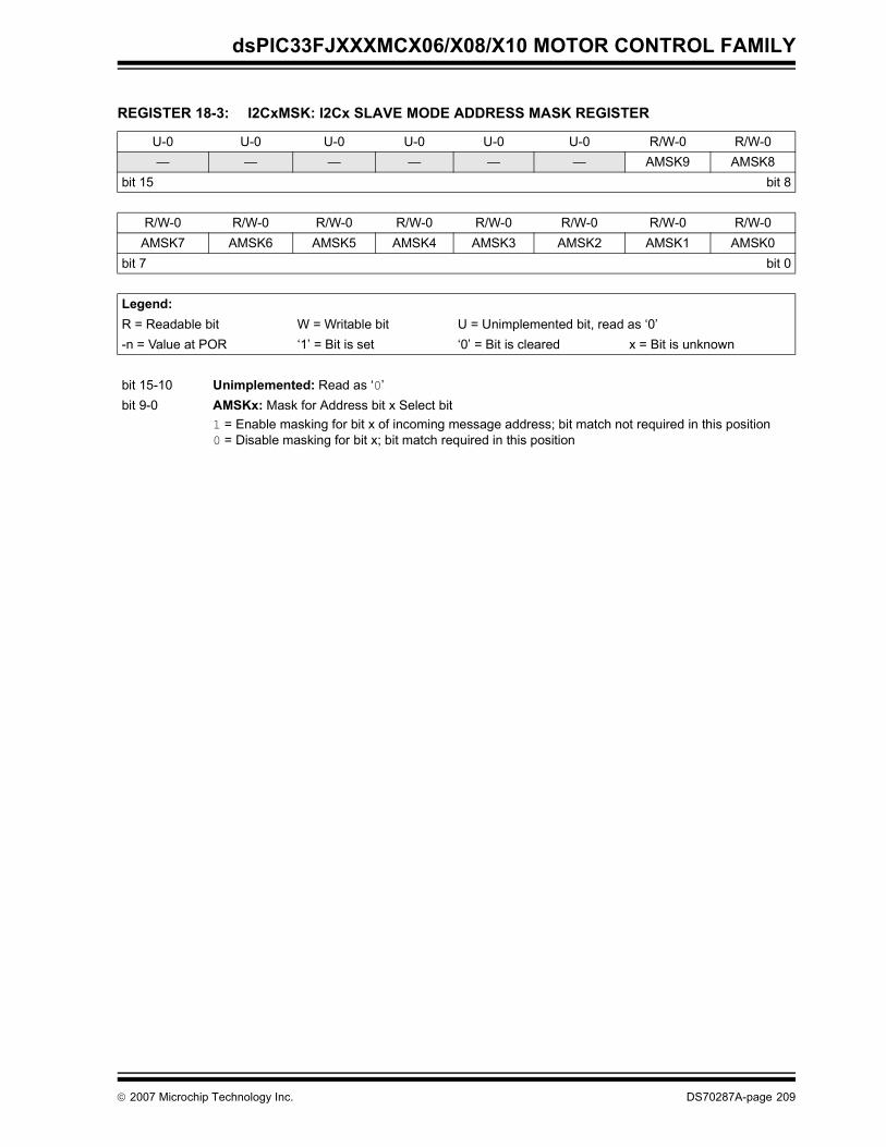
dsPIC33FJXXXMCX06/X08/X10 MOTOR CONTROL FAMILY
REGISTER 18-3: I2CxMSK: I2Cx SLAVE MODE ADDRESS MASK REGISTER
U-0 U-0 U-0 U-0 U-0 U-0 R/W-0 R/W-0— — — — — — AMSK9 AMSK8
bit 15 bit 8
R/W-0 R/W-0 R/W-0 R/W-0 R/W-0 R/W-0 R/W-0 R/W-0AMSK7 AMSK6 AMSK5 AMSK4 AMSK3 AMSK2 AMSK1 AMSK0
bit 7 bit 0
Legend:R = Readable bit W = Writable bit U = Unimplemented bit, read as ‘0’-n = Value at POR ‘1’ = Bit is set ‘0’ = Bit is cleared x = Bit is unknown
bit 15-10 Unimplemented: Read as ‘0’bit 9-0 AMSKx: Mask for Address bit x Select bit
1 = Enable masking for bit x of incoming message address; bit match not required in this position0 = Disable masking for bit x; bit match required in this position
© 2007 Microchip Technology Inc. DS70287A-page 209

dsPIC33FJXXXMCX06/X08/X10 MOTOR CONTROL FAMILY
NOTES:
DS70287A-page 210 © 2007 Microchip Technology Inc.
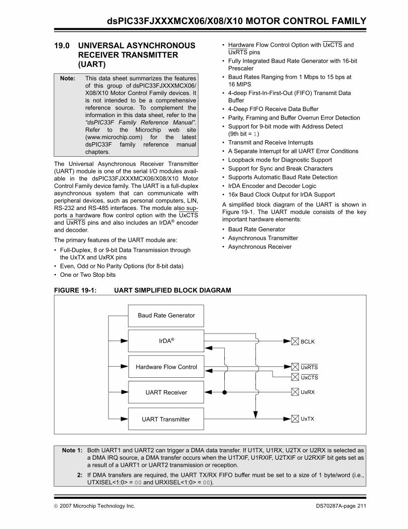
dsPIC33FJXXXMCX06/X08/X10 MOTOR CONTROL FAMILY
19.0 UNIVERSAL ASYNCHRONOUS RECEIVER TRANSMITTER (UART)
The Universal Asynchronous Receiver Transmitter(UART) module is one of the serial I/O modules avail-able in the dsPIC33FJXXXMCX06/X08/X10 MotorControl Family device family. The UART is a full-duplexasynchronous system that can communicate withperipheral devices, such as personal computers, LIN,RS-232 and RS-485 interfaces. The module also sup-ports a hardware flow control option with the UxCTSand UxRTS pins and also includes an IrDA® encoderand decoder.
The primary features of the UART module are:
• Full-Duplex, 8 or 9-bit Data Transmission through the UxTX and UxRX pins
• Even, Odd or No Parity Options (for 8-bit data)• One or Two Stop bits
• Hardware Flow Control Option with UxCTS and UxRTS pins
• Fully Integrated Baud Rate Generator with 16-bit Prescaler
• Baud Rates Ranging from 1 Mbps to 15 bps at 16 MIPS
• 4-deep First-In-First-Out (FIFO) Transmit Data Buffer
• 4-Deep FIFO Receive Data Buffer• Parity, Framing and Buffer Overrun Error Detection• Support for 9-bit mode with Address Detect
(9th bit = 1)• Transmit and Receive Interrupts• A Separate Interrupt for all UART Error Conditions• Loopback mode for Diagnostic Support• Support for Sync and Break Characters• Supports Automatic Baud Rate Detection• IrDA Encoder and Decoder Logic• 16x Baud Clock Output for IrDA Support
A simplified block diagram of the UART is shown inFigure 19-1. The UART module consists of the keyimportant hardware elements:
• Baud Rate Generator• Asynchronous Transmitter• Asynchronous Receiver
FIGURE 19-1: UART SIMPLIFIED BLOCK DIAGRAM
Note: This data sheet summarizes the featuresof this group of dsPIC33FJXXXMCX06/X08/X10 Motor Control Family devices. Itis not intended to be a comprehensivereference source. To complement theinformation in this data sheet, refer to the“dsPIC33F Family Reference Manual”.Refer to the Microchip web site(www.microchip.com) for the latestdsPIC33F family reference manualchapters.
Note 1: Both UART1 and UART2 can trigger a DMA data transfer. If U1TX, U1RX, U2TX or U2RX is selected asa DMA IRQ source, a DMA transfer occurs when the U1TXIF, U1RXIF, U2TXIF or U2RXIF bit gets set asa result of a UART1 or UART2 transmission or reception.
2: If DMA transfers are required, the UART TX/RX FIFO buffer must be set to a size of 1 byte/word (i.e.,UTXISEL<1:0> = 00 and URXISEL<1:0> = 00).
UxRX
Hardware Flow Control
UART Receiver
UART Transmitter UxTX
BCLK
Baud Rate Generator
UxRTS
IrDA®
UxCTS
© 2007 Microchip Technology Inc. DS70287A-page 211
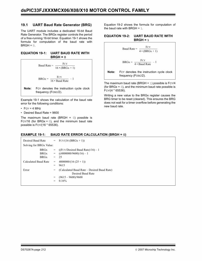
dsPIC33FJXXXMCX06/X08/X10 MOTOR CONTROL FAMILY
19.1 UART Baud Rate Generator (BRG)The UART module includes a dedicated 16-bit BaudRate Generator. The BRGx register controls the periodof a free-running 16-bit timer. Equation 19-1 shows theformula for computation of the baud rate withBRGH = 0.
EQUATION 19-1: UART BAUD RATE WITH BRGH = 0
Example 19-1 shows the calculation of the baud rateerror for the following conditions:
• FCY = 4 MHz • Desired Baud Rate = 9600
The maximum baud rate (BRGH = 0) possible isFCY/16 (for BRGx = 0), and the minimum baud ratepossible is FCY/(16 * 65536).
Equation 19-2 shows the formula for computation ofthe baud rate with BRGH = 1.
EQUATION 19-2: UART BAUD RATE WITH BRGH = 1
The maximum baud rate (BRGH = 1) possible is FCY/4(for BRGx = 0), and the minimum baud rate possible isFCY/(4 * 65536).
Writing a new value to the BRGx register causes theBRG timer to be reset (cleared). This ensures the BRGdoes not wait for a timer overflow before generating thenew baud rate.
EXAMPLE 19-1: BAUD RATE ERROR CALCULATION (BRGH = 0)
Note: FCY denotes the instruction cycle clockfrequency (FOSC/2).
Baud Rate = FCY
16 • (BRGx + 1)
FCY16 • Baud Rate
BRGx = – 1
Note: FCY denotes the instruction cycle clockfrequency (FOSC/2).
Baud Rate = FCY
4 • (BRGx + 1)
FCY4 • Baud Rate
BRGx = – 1
Desired Baud Rate = FCY/(16 (BRGx + 1)) Solving for BRGx Value:
BRGx = ((FCY/Desired Baud Rate)/16) – 1BRGx = ((4000000/9600)/16) – 1 BRGx = 25
Calculated Baud Rate = 4000000/(16 (25 + 1)) = 9615
Error = (Calculated Baud Rate – Desired Baud Rate)Desired Baud Rate
= (9615 – 9600)/9600 = 0.16%
DS70287A-page 212 © 2007 Microchip Technology Inc.
dsPIC33FJXXXMCX06/X08/X10 MOTOR CONTROL FAMILY
19.2 Transmitting in 8-bit Data Mode1. Set up the UART:
a) Write appropriate values for data, parity andStop bits.
b) Write appropriate baud rate value to theBRGx register.
c) Set up transmit and receive interrupt enableand priority bits.
2. Enable the UART.3. Set the UTXEN bit (causes a transmit interrupt).4. Write data byte to lower byte of UxTXREG word.
The value will be immediately transferred to theTransmit Shift Register (TSR) and the serial bitstream will start shifting out with the next risingedge of the baud clock.
5. Alternately, the data byte may be transferredwhile UTXEN = 0, and then the user may setUTXEN. This will cause the serial bit stream tobegin immediately because the baud clock willstart from a cleared state.
6. A transmit interrupt will be generated as perinterrupt control bits, UTXISEL<1:0>.
19.3 Transmitting in 9-bit Data Mode1. Set up the UART (as described in Section 19.2
“Transmitting in 8-bit Data Mode”).2. Enable the UART.3. Set the UTXEN bit (causes a transmit interrupt).4. Write UxTXREG as a 16-bit value only.5. A word write to UxTXREG triggers the transfer
of the 9-bit data to the TSR. Serial bit stream willstart shifting out with the first rising edge of thebaud clock.
6. A transmit interrupt will be generated as per thesetting of control bits, UTXISEL<1:0>.
19.4 Break and Sync Transmit Sequence
The following sequence will send a message frameheader made up of a Break, followed by an auto-baudSync byte.
1. Configure the UART for the desired mode.2. Set UTXEN and UTXBRK – sets up the Break
character.3. Load the UxTXREG register with a dummy
character to initiate transmission (value isignored).
4. Write 0x55 to UxTXREG – loads Sync characterinto the transmit FIFO.
5. After the Break has been sent, the UTXBRK bitis reset by hardware. The Sync character nowtransmits.
19.5 Receiving in 8-bit or 9-bit Data Mode
1. Set up the UART (as described in Section 19.2“Transmitting in 8-bit Data Mode”).
2. Enable the UART.3. A receive interrupt will be generated when one
or more data characters have been received asper interrupt control bits, URXISEL<1:0>.
4. Read the OERR bit to determine if an overrunerror has occurred. The OERR bit must be resetin software.
5. Read UxRXREG.
The act of reading the UxRXREG character will movethe next character to the top of the receive FIFO,including a new set of PERR and FERR values.
19.6 Flow Control Using UxCTS and UxRTS Pins
UARTx Clear to Send (UxCTS) and Request to Send(UxRTS) are the two hardware controlled active-lowpins that are associated with the UART module. Thesetwo pins allow the UART to operate in Simplex andFlow Control modes. They are implemented to controlthe transmission and the reception between the DataTerminal Equipment (DTE). The UEN<1:0> bits in theUxMODE register configures these pins.
19.7 Infrared SupportThe UART module provides two types of infrared UARTsupport:
• IrDA clock output to support external IrDA encoder and decoder device (legacy module support)
• Full implementation of the IrDA encoder and decoder.
19.7.1 EXTERNAL IrDA SUPPORT – IrDA CLOCK OUTPUT
To support external IrDA encoder and decoder devices,the BCLK pin (same as the UxRTS pin) can beconfigured to generate the 16x baud clock. WithUEN<1:0> = 11, the BCLK pin will output the 16x baudclock if the UART module is enabled; it can be used tosupport the IrDA codec chip.
19.7.2 BUILT-IN IrDA ENCODER AND DECODER
The UART has full implementation of the IrDA encoderand decoder as part of the UART module. The built-inIrDA encoder and decoder functionality is enabledusing the IREN bit (UxMODE<12>). When enabled(IREN = 1), the receive pin (UxRX) acts as the inputfrom the infrared receiver. The transmit pin (UxTX) actsas the output to the infrared transmitter.
© 2007 Microchip Technology Inc. DS70287A-page 213
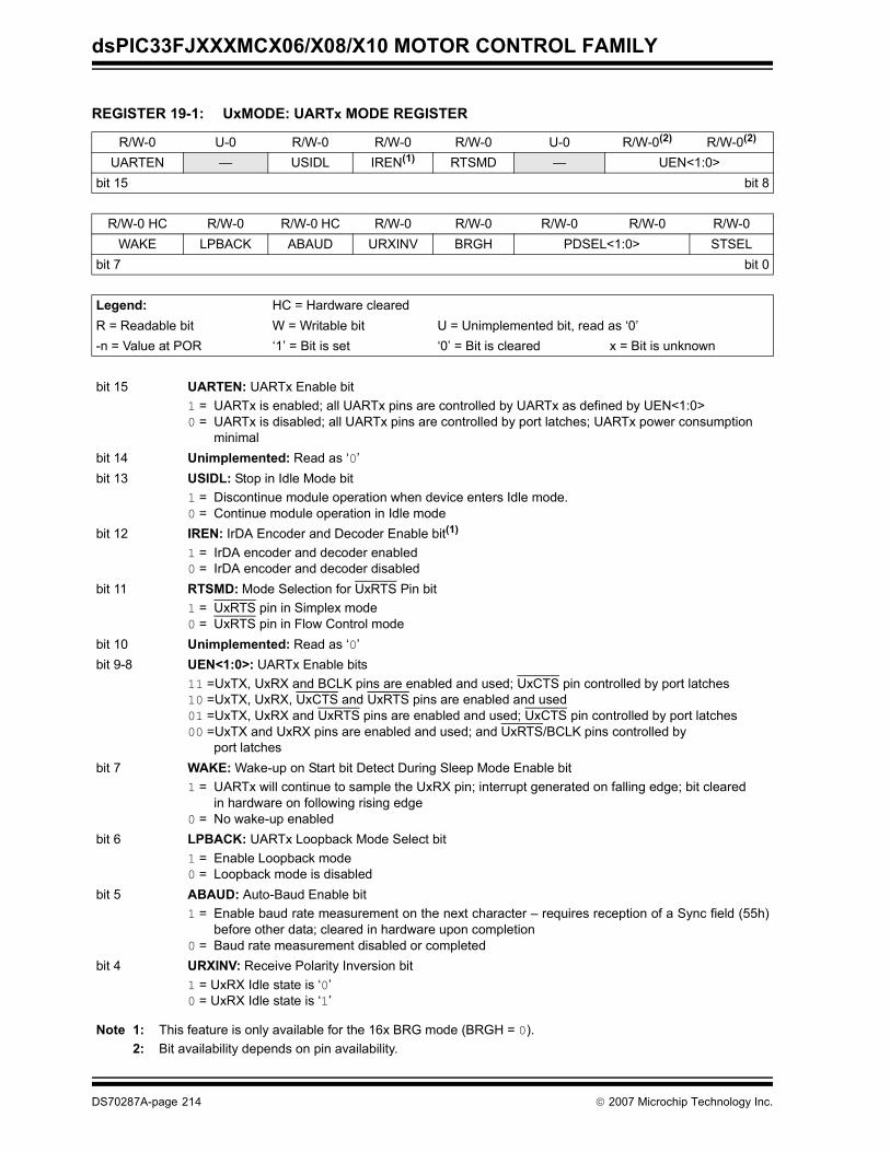
dsPIC33FJXXXMCX06/X08/X10 MOTOR CONTROL FAMILY
REGISTER 19-1: UxMODE: UARTx MODE REGISTER
R/W-0 U-0 R/W-0 R/W-0 R/W-0 U-0 R/W-0(2) R/W-0(2)
UARTEN — USIDL IREN(1) RTSMD — UEN<1:0>bit 15 bit 8
R/W-0 HC R/W-0 R/W-0 HC R/W-0 R/W-0 R/W-0 R/W-0 R/W-0WAKE LPBACK ABAUD URXINV BRGH PDSEL<1:0> STSEL
bit 7 bit 0
Legend: HC = Hardware clearedR = Readable bit W = Writable bit U = Unimplemented bit, read as ‘0’-n = Value at POR ‘1’ = Bit is set ‘0’ = Bit is cleared x = Bit is unknown
bit 15 UARTEN: UARTx Enable bit1 = UARTx is enabled; all UARTx pins are controlled by UARTx as defined by UEN<1:0>0 = UARTx is disabled; all UARTx pins are controlled by port latches; UARTx power consumption
minimalbit 14 Unimplemented: Read as ‘0’bit 13 USIDL: Stop in Idle Mode bit
1 = Discontinue module operation when device enters Idle mode.0 = Continue module operation in Idle mode
bit 12 IREN: IrDA Encoder and Decoder Enable bit(1)
1 = IrDA encoder and decoder enabled0 = IrDA encoder and decoder disabled
bit 11 RTSMD: Mode Selection for UxRTS Pin bit1 = UxRTS pin in Simplex mode0 = UxRTS pin in Flow Control mode
bit 10 Unimplemented: Read as ‘0’bit 9-8 UEN<1:0>: UARTx Enable bits
11 =UxTX, UxRX and BCLK pins are enabled and used; UxCTS pin controlled by port latches10 =UxTX, UxRX, UxCTS and UxRTS pins are enabled and used01 =UxTX, UxRX and UxRTS pins are enabled and used; UxCTS pin controlled by port latches00 =UxTX and UxRX pins are enabled and used; and UxRTS/BCLK pins controlled by
port latchesbit 7 WAKE: Wake-up on Start bit Detect During Sleep Mode Enable bit
1 = UARTx will continue to sample the UxRX pin; interrupt generated on falling edge; bit cleared in hardware on following rising edge
0 = No wake-up enabledbit 6 LPBACK: UARTx Loopback Mode Select bit
1 = Enable Loopback mode0 = Loopback mode is disabled
bit 5 ABAUD: Auto-Baud Enable bit1 = Enable baud rate measurement on the next character – requires reception of a Sync field (55h)
before other data; cleared in hardware upon completion0 = Baud rate measurement disabled or completed
bit 4 URXINV: Receive Polarity Inversion bit 1 = UxRX Idle state is ‘0’0 = UxRX Idle state is ‘1’
Note 1: This feature is only available for the 16x BRG mode (BRGH = 0).2: Bit availability depends on pin availability.
DS70287A-page 214 © 2007 Microchip Technology Inc.
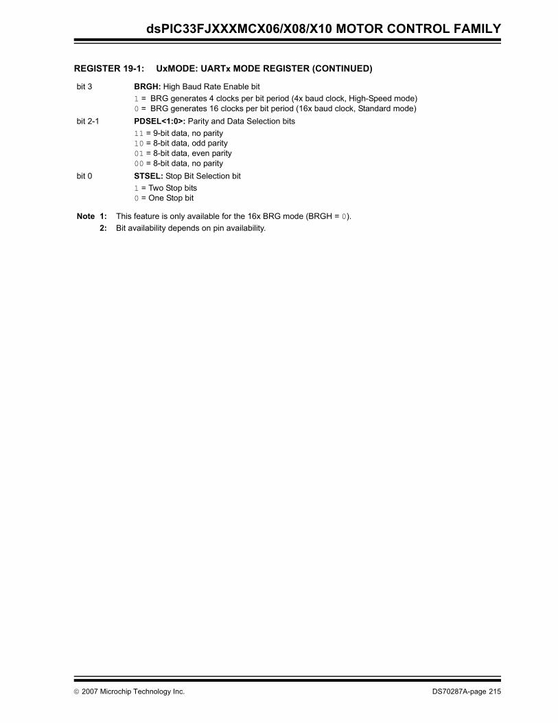
dsPIC33FJXXXMCX06/X08/X10 MOTOR CONTROL FAMILY
bit 3 BRGH: High Baud Rate Enable bit1 = BRG generates 4 clocks per bit period (4x baud clock, High-Speed mode)0 = BRG generates 16 clocks per bit period (16x baud clock, Standard mode)
bit 2-1 PDSEL<1:0>: Parity and Data Selection bits11 = 9-bit data, no parity10 = 8-bit data, odd parity01 = 8-bit data, even parity00 = 8-bit data, no parity
bit 0 STSEL: Stop Bit Selection bit1 = Two Stop bits0 = One Stop bit
REGISTER 19-1: UxMODE: UARTx MODE REGISTER (CONTINUED)
Note 1: This feature is only available for the 16x BRG mode (BRGH = 0).2: Bit availability depends on pin availability.
© 2007 Microchip Technology Inc. DS70287A-page 215
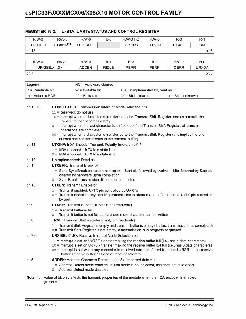
dsPIC33FJXXXMCX06/X08/X10 MOTOR CONTROL FAMILY
REGISTER 19-2: UxSTA: UARTx STATUS AND CONTROL REGISTER
R/W-0 R/W-0 R/W-0 U-0 R/W-0 HC R/W-0 R-0 R-1UTXISEL1 UTXINV(1) UTXISEL0 — UTXBRK UTXEN UTXBF TRMT
bit 15 bit 8
R/W-0 R/W-0 R/W-0 R-1 R-0 R-0 R/C-0 R-0URXISEL<1:0> ADDEN RIDLE PERR FERR OERR URXDA
bit 7 bit 0
Legend: HC = Hardware clearedR = Readable bit W = Writable bit U = Unimplemented bit, read as ‘0’-n = Value at POR ‘1’ = Bit is set ‘0’ = Bit is cleared x = Bit is unknown
bit 15,13 UTXISEL<1:0>: Transmission Interrupt Mode Selection bits 11 =Reserved; do not use10 =Interrupt when a character is transferred to the Transmit Shift Register, and as a result, the
transmit buffer becomes empty01 =Interrupt when the last character is shifted out of the Transmit Shift Register; all transmit
operations are completed00 =Interrupt when a character is transferred to the Transmit Shift Register (this implies there is
at least one character open in the transmit buffer)bit 14 UTXINV: IrDA Encoder Transmit Polarity Inversion bit(1)
1 = IrDA encoded, UxTX Idle state is ‘1’0 = IrDA encoded, UxTX Idle state is ‘0’
bit 12 Unimplemented: Read as ‘0’bit 11 UTXBRK: Transmit Break bit
1 = Send Sync Break on next transmission – Start bit, followed by twelve ‘0’ bits, followed by Stop bit;cleared by hardware upon completion
0 = Sync Break transmission disabled or completedbit 10 UTXEN: Transmit Enable bit
1 = Transmit enabled, UxTX pin controlled by UARTx0 = Transmit disabled, any pending transmission is aborted and buffer is reset. UxTX pin controlled
by port.bit 9 UTXBF: Transmit Buffer Full Status bit (read-only)
1 = Transmit buffer is full0 = Transmit buffer is not full, at least one more character can be written
bit 8 TRMT: Transmit Shift Register Empty bit (read-only)1 = Transmit Shift Register is empty and transmit buffer is empty (the last transmission has completed)0 = Transmit Shift Register is not empty, a transmission is in progress or queued
bit 7-6 URXISEL<1:0>: Receive Interrupt Mode Selection bits 11 =Interrupt is set on UxRSR transfer making the receive buffer full (i.e., has 4 data characters)10 =Interrupt is set on UxRSR transfer making the receive buffer 3/4 full (i.e., has 3 data characters)0x =Interrupt is set when any character is received and transferred from the UxRSR to the receive
buffer. Receive buffer has one or more characters.bit 5 ADDEN: Address Character Detect bit (bit 8 of received data = 1)
1 = Address Detect mode enabled. If 9-bit mode is not selected, this does not take effect.0 = Address Detect mode disabled
Note 1: Value of bit only affects the transmit properties of the module when the IrDA encoder is enabled (IREN = 1).
DS70287A-page 216 © 2007 Microchip Technology Inc.
dsPIC33FJXXXMCX06/X08/X10 MOTOR CONTROL FAMILY
bit 4 RIDLE: Receiver Idle bit (read-only)1 = Receiver is Idle0 = Receiver is active
bit 3 PERR: Parity Error Status bit (read-only)1 = Parity error has been detected for the current character (character at the top of the receive FIFO)0 = Parity error has not been detected
bit 2 FERR: Framing Error Status bit (read-only)1 = Framing error has been detected for the current character (character at the top of the receive
FIFO)0 = Framing error has not been detected
bit 1 OERR: Receive Buffer Overrun Error Status bit (read/clear only)1 = Receive buffer has overflowed0 = Receive buffer has not overflowed. Clearing a previously set OERR bit (1 → 0 transition) will reset
the receiver buffer and the UxRSR to the empty state.bit 0 URXDA: Receive Buffer Data Available bit (read-only)
1 = Receive buffer has data, at least one more character can be read0 = Receive buffer is empty
REGISTER 19-2: UxSTA: UARTx STATUS AND CONTROL REGISTER (CONTINUED)
Note 1: Value of bit only affects the transmit properties of the module when the IrDA encoder is enabled (IREN = 1).
© 2007 Microchip Technology Inc. DS70287A-page 217

dsPIC33FJXXXMCX06/X08/X10 MOTOR CONTROL FAMILY
NOTES:
DS70287A-page 218 © 2007 Microchip Technology Inc.
dsPIC33FJXXXMCX06/X08/X10 MOTOR CONTROL FAMILY
20.0 ENHANCED CAN MODULE
20.1 Overview The Enhanced Controller Area Network (ECAN™)module is a serial interface, useful for communicatingwith other CAN modules or microcontroller devices.This interface/protocol was designed to allow commu-nications within noisy environments. ThedsPIC33FJXXXMCX06/X08/X10 Motor Control Familydevices contain up to two ECAN modules.
The CAN module is a communication controller imple-menting the CAN 2.0 A/B protocol, as defined in theBOSCH specification. The module will support CAN 1.2,CAN 2.0A, CAN 2.0B Passive and CAN 2.0B Activeversions of the protocol. The module implementation isa full CAN system. The CAN specification is not coveredwithin this data sheet. The reader may refer to theBOSCH CAN specification for further details.
The module features are as follows:
• Implementation of the CAN protocol, CAN 1.2, CAN 2.0A and CAN 2.0B
• Standard and extended data frames• 0-8 bytes data length• Programmable bit rate up to 1 Mbit/sec• Automatic response to remote transmission
requests• Up to 8 transmit buffers with application specified
prioritization and abort capability (each buffer may contain up to 8 bytes of data)
• Up to 32 receive buffers (each buffer may contain up to 8 bytes of data)
• Up to 16 full (standard/extended identifier) acceptance filters
• 3 full acceptance filter masks• DeviceNet™ addressing support• Programmable wake-up functionality with
integrated low-pass filter• Programmable Loopback mode supports self-test
operation• Signaling via interrupt capabilities for all CAN
receiver and transmitter error states• Programmable clock source• Programmable link to input capture module (IC2
for both CAN1 and CAN2) for time-stamping and network synchronization
• Low-power Sleep and Idle mode
The CAN bus module consists of a protocol engine andmessage buffering/control. The CAN protocol enginehandles all functions for receiving and transmittingmessages on the CAN bus. Messages are transmittedby first loading the appropriate data registers. Statusand errors can be checked by reading the appropriateregisters. Any message detected on the CAN bus ischecked for errors and then matched against filters tosee if it should be received and stored in one of thereceive registers.
20.2 Frame TypesThe CAN module transmits various types of frameswhich include data messages, or remote transmissionrequests initiated by the user, as other frames that areautomatically generated for control purposes. Thefollowing frame types are supported:
• Standard Data Frame:A standard data frame is generated by a nodewhen the node wishes to transmit data. It includesan 11-bit Standard Identifier (SID), but not an 18-bit Extended Identifier (EID).
• Extended Data Frame:An extended data frame is similar to a standarddata frame, but includes an extended identifier aswell.
• Remote Frame:It is possible for a destination node to request thedata from the source. For this purpose, thedestination node sends a remote frame with anidentifier that matches the identifier of the requireddata frame. The appropriate data source node willthen send a data frame as a response to thisremote request.
• Error Frame:An error frame is generated by any node thatdetects a bus error. An error frame consists of twofields: an error flag field and an error delimiterfield.
• Overload Frame: An overload frame can be generated by a node asa result of two conditions. First, the node detectsa dominant bit during interframe space which is anillegal condition. Second, due to internal condi-tions, the node is not yet able to start reception ofthe next message. A node may generate a maxi-mum of 2 sequential overload frames to delay thestart of the next message.
• Interframe Space:Interframe space separates a proceeding frame(of whatever type) from a following data or remoteframe.
Note: This data sheet summarizes the featuresof this group of dsPIC33FJXXXMCX06/X08/X10 Motor Control Family devices. Itis not intended to be a comprehensivereference source. To complement theinformation in this data sheet, refer to the“dsPIC33F Family Reference Manual”.Refer to the Microchip web site(www.microchip.com) for the latestdsPIC33F family reference manualchapters.
© 2007 Microchip Technology Inc. DS70287A-page 219
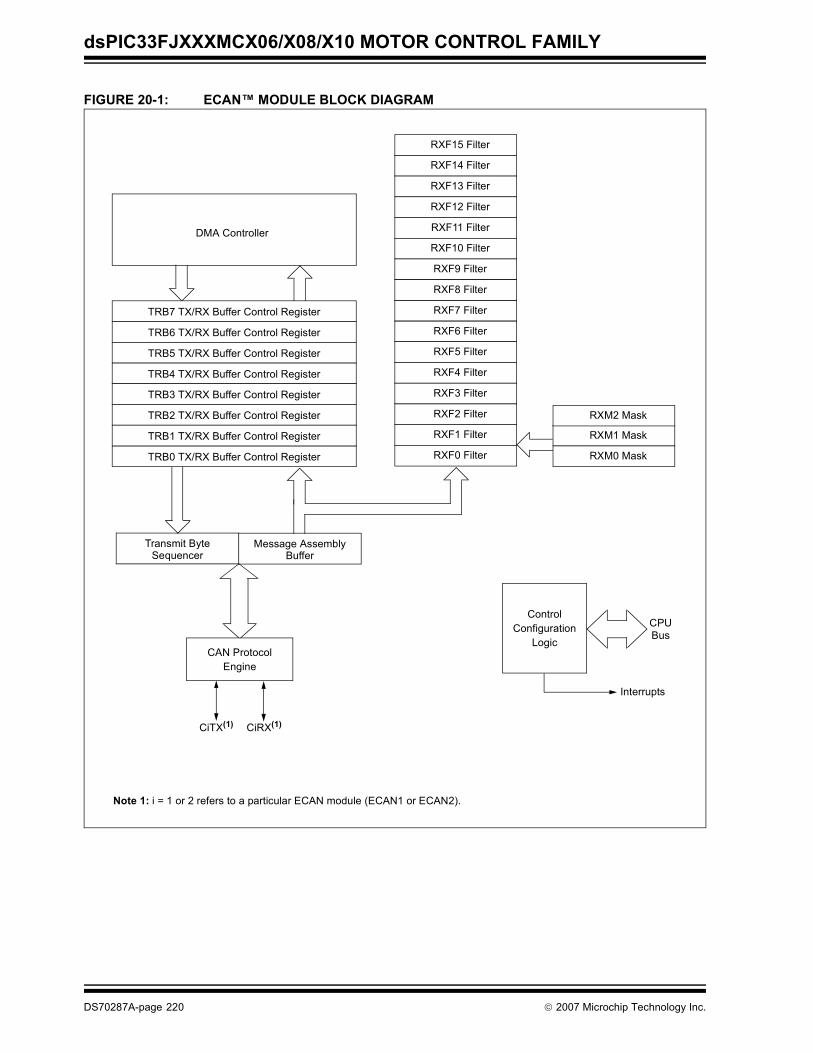
dsPIC33FJXXXMCX06/X08/X10 MOTOR CONTROL FAMILY
FIGURE 20-1: ECAN™ MODULE BLOCK DIAGRAM
Message Assembly
CAN ProtocolEngine
CiTX(1)
Buffer
CiRX(1)
RXF14 Filter
RXF13 Filter
RXF12 Filter
RXF11 Filter
RXF10 Filter
RXF9 Filter
RXF8 Filter
RXF7 Filter
RXF6 Filter
RXF5 Filter
RXF4 Filter
RXF3 Filter
RXF2 Filter
RXF1 Filter
RXF0 Filter
Transmit ByteSequencer
RXM1 Mask
RXM0 Mask
ControlConfiguration
Logic
CPUBus
Interrupts
TRB0 TX/RX Buffer Control Register
DMA Controller
RXF15 Filter
RXM2 Mask
TRB7 TX/RX Buffer Control Register
TRB6 TX/RX Buffer Control Register
TRB5 TX/RX Buffer Control Register
TRB4 TX/RX Buffer Control Register
TRB3 TX/RX Buffer Control Register
TRB2 TX/RX Buffer Control Register
TRB1 TX/RX Buffer Control Register
Note 1: i = 1 or 2 refers to a particular ECAN module (ECAN1 or ECAN2).
DS70287A-page 220 © 2007 Microchip Technology Inc.

dsPIC33FJXXXMCX06/X08/X10 MOTOR CONTROL FAMILY
20.3 Modes of OperationThe CAN module can operate in one of several operationmodes selected by the user. These modes include:• Initialization Mode• Disable Mode• Normal Operation Mode• Listen Only Mode• Listen All Messages Mode• Loopback Mode
Modes are requested by setting the REQOP<2:0> bits(CiCTRL1<10:8>). Entry into a mode is Acknowledgedby monitoring the OPMODE<2:0> bits(CiCTRL1<7:5>). The module will not change the modeand the OPMODE bits until a change in mode isacceptable, generally during bus Idle time, which isdefined as at least 11 consecutive recessive bits.
20.3.1 INITIALIZATION MODEIn the Initialization mode, the module will not transmit orreceive. The error counters are cleared and the inter-rupt flags remain unchanged. The programmer willhave access to Configuration registers that are accessrestricted in other modes. The module will protect theuser from accidentally violating the CAN protocolthrough programming errors. All registers which controlthe configuration of the module can not be modifiedwhile the module is on-line. The CAN module will notbe allowed to enter the Configuration mode while atransmission is taking place. The Configuration modeserves as a lock to protect the following registers:• All Module Control Registers• Baud Rate and Interrupt Configuration Registers • Bus Timing Registers • Identifier Acceptance Filter Registers • Identifier Acceptance Mask Registers
20.3.2 DISABLE MODEIn Disable mode, the module will not transmit orreceive. The module has the ability to set the WAKIF bitdue to bus activity, however, any pending interrupts willremain and the error counters will retain their value.
If the REQOP<2:0> bits (CiCTRL1<10:8>) = 001, themodule will enter the Module Disable mode. If the moduleis active, the module will wait for 11 recessive bits on theCAN bus, detect that condition as an Idle bus, thenaccept the module disable command. When theOPMODE<2:0> bits (CiCTRL1<7:5>) = 001, that indi-cates whether the module successfully went into ModuleDisable mode. The I/O pins will revert to normal I/Ofunction when the module is in the Module Disable mode.
The module can be programmed to apply a low-passfilter function to the CiRX input line while the module orthe CPU is in Sleep mode. The WAKFIL bit(CiCFG2<14>) enables or disables the filter.
20.3.3 NORMAL OPERATION MODENormal Operation mode is selected whenREQOP<2:0> = 000. In this mode, the module isactivated and the I/O pins will assume the CAN busfunctions. The module will transmit and receive CANbus messages via the CiTX and CiRX pins.
20.3.4 LISTEN ONLY MODEIf the Listen Only mode is activated, the module on theCAN bus is passive. The transmitter buffers revert tothe port I/O function. The receive pins remain inputs.For the receiver, no error flags or Acknowledge signalsare sent. The error counters are deactivated in thisstate. The Listen Only mode can be used for detectingthe baud rate on the CAN bus. To use this, it is neces-sary that there are at least two further nodes thatcommunicate with each other.
20.3.5 LISTEN ALL MESSAGES MODEThe module can be set to ignore all errors and receiveany message. The Listen All Messages mode is acti-vated by setting REQOP<2:0> = ‘111’. In this mode,the data which is in the message assembly buffer, untilthe time an error occurred, is copied in the receivebuffer and can be read via the CPU interface.
20.3.6 LOOPBACK MODEIf the Loopback mode is activated, the module will con-nect the internal transmit signal to the internal receivesignal at the module boundary. The transmit andreceive pins revert to their port I/O function.
20.4 Message Reception
20.4.1 RECEIVE BUFFERSThe CAN bus module has up to 32 receive buffers,located in DMA RAM. The first 8 buffers need to beconfigured as receive buffers by clearing thecorresponding TX/RX buffer selection (TXENn) bit in aCiTRmnCON register. The overall size of the CANbuffer area in DMA RAM is selectable by the user andis defined by the DMABS<2:0> bits(CiFCTRL<15:13>). The first 16 buffers can beassigned to receive filters, while the rest can be usedonly as a FIFO buffer.
Note: Typically, if the CAN module is allowed totransmit in a particular mode of operationand a transmission is requested immedi-ately after the CAN module has beenplaced in that mode of operation, the mod-ule waits for 11 consecutive recessive bitson the bus before starting transmission. Ifthe user switches to Disable mode withinthis 11-bit period, then this transmission isaborted and the corresponding TXABT bitis set and TXREQ bit is cleared.
© 2007 Microchip Technology Inc. DS70287A-page 221
dsPIC33FJXXXMCX06/X08/X10 MOTOR CONTROL FAMILY
An additional buffer is always committed to monitoringthe bus for incoming messages. This buffer is called theMessage Assembly Buffer (MAB).
All messages are assembled by the MAB and are trans-ferred to the buffers only if the acceptance filter criterionare met. When a message is received, the RBIF flag(CiINTF<1>) will be set. The user would then need toinspect the CiVEC and/or CiRXFUL1 register to deter-mine which filter and buffer caused the interrupt to getgenerated. The RBIF bit can only be set by the modulewhen a message is received. The bit is cleared by theuser when it has completed processing the message inthe buffer. If the RBIE bit is set, an interrupt will begenerated when a message is received.
20.4.2 FIFO BUFFER MODEThe ECAN module provides FIFO buffer functionality ifthe buffer pointer for a filter has a value of ‘1111’. In thismode, the results of a hit on that buffer will write to thenext available buffer location within the FIFO.
The CiFCTRL register defines the size of the FIFO. TheFSA<4:0> bits in this register define the start of theFIFO buffers. The end of the FIFO is defined by theDMABS<2:0> bits if DMA is enabled. Thus, FIFO sizesup to 32 buffers are supported.
20.4.3 MESSAGE ACCEPTANCE FILTERSThe message acceptance filters and masks are used todetermine if a message in the message assemblybuffer should be loaded into either of the receive buff-ers. Once a valid message has been received into theMessage Assembly Buffer (MAB), the identifier fields ofthe message are compared to the filter values. If thereis a match, that message will be loaded into theappropriate receive buffer. Each filter is associated witha buffer pointer (FnBP<3:0>), which is used to link thefilter to one of 16 receive buffers.
The acceptance filter looks at incoming messages forthe IDE bit (CiTRBnSID<0>) to determine how to com-pare the identifiers. If the IDE bit is clear, the messageis a standard frame and only filters with the EXIDE bit(CiRXFnSID<3>) clear are compared. If the IDE bit isset, the message is an extended frame, and only filterswith the EXIDE bit set are compared.
20.4.4 MESSAGE ACCEPTANCE FILTER MASKS
The mask bits essentially determine which bits to applythe filter to. If any mask bit is set to a zero, then that bitwill automatically be accepted regardless of the filterbit. There are three programmable acceptance filtermasks associated with the receive buffers. Any ofthese three masks can be linked to each filter by select-ing the desired mask in the FnMSK<1:0> bits in theappropriate CiFMSKSELn register.
20.4.5 RECEIVE ERRORSThe CAN module will detect the following receiveerrors:
• Cyclic Redundancy Check (CRC) Error• Bit Stuffing Error• Invalid Message Receive Error
These receive errors do not generate an interrupt.However, the receive error counter is incremented byone in case one of these errors occur. The RXWAR bit(CiINTF<9>) indicates that the receive error counterhas reached the CPU warning limit of 96 and aninterrupt is generated.
20.4.6 RECEIVE INTERRUPTSReceive interrupts can be divided into 3 major groups,each including various conditions that generateinterrupts:
• Receive Interrupt:A message has been successfully received andloaded into one of the receive buffers. This inter-rupt is activated immediately after receiving theEnd-of-Frame (EOF) field. Reading the RXnIF flagwill indicate which receive buffer caused theinterrupt.
• Wake-up Interrupt:The CAN module has woken up from Disablemode or the device has woken up from Sleepmode.
• Receive Error Interrupts:A receive error interrupt will be indicated by theERRIF bit. This bit shows that an error conditionoccurred. The source of the error can be deter-mined by checking the bits in the CAN InterruptFlag register, CiINTF.
- Invalid Message Received:If any type of error occurred during reception ofthe last message, an error will be indicated bythe IVRIF bit.
- Receiver Overrun:The RBOVIF bit (CiINTF<2>) indicates that anoverrun condition occurred.
- Receiver Warning: The RXWAR bit indicates that the receive errorcounter (RERRCNT<7:0>) has reached thewarning limit of 96.
- Receiver Error Passive:The RXEP bit indicates that the receive errorcounter has exceeded the error passive limit of127 and the module has gone into error passivestate.
DS70287A-page 222 © 2007 Microchip Technology Inc.
dsPIC33FJXXXMCX06/X08/X10 MOTOR CONTROL FAMILY
20.5 Message Transmission
20.5.1 TRANSMIT BUFFERSThe CAN module has up to eight transmit buffers,located in DMA RAM. These 8 buffers need to be con-figured as transmit buffers by setting the correspondingTX/RX buffer selection (TXENn or TXENm) bit in aCiTRmnCON register. The overall size of the CANbuffer area in DMA RAM is selectable by the user andis defined by the DMABS<2:0> bits(CiFCTRL<15:13>).
Each transmit buffer occupies 16 bytes of data. Eight ofthe bytes are the maximum 8 bytes of the transmittedmessage. Five bytes hold the standard and extendedidentifiers and other message arbitration information.The last byte is unused.
20.5.2 TRANSMIT MESSAGE PRIORITYTransmit priority is a prioritization within each node ofthe pending transmittable messages. There are fourlevels of transmit priority. If the TXnPRI<1:0> bits (inCiTRmnCON) for a particular message buffer areset to ‘11’, that buffer has the highest priority. If theTXnPRI<1:0> bits for a particular message bufferare set to ‘10’ or ‘01’, that buffer has an intermediatepriority. If the TXnPRI<1:0> bits for a particularmessage buffer are ‘00’, that buffer has the lowest pri-ority. If two or more pending messages have the samepriority, the messages are transmitted in decreasingorder of buffer index.
20.5.3 TRANSMISSION SEQUENCETo initiate transmission of the message, the TXREQn bit(in CiTRmnCON) must be set. The CAN bus moduleresolves any timing conflicts between the setting of theTXREQn bit and the Start-of-Frame (SOF), ensuring thatif the priority was changed, it is resolved correctly beforethe SOF occurs. When TXREQn is set, the TXABTn,TXLARBn and TXERRn flag bits are automaticallycleared.
Setting the TXREQn bit simply flags a message bufferas enqueued for transmission. When the moduledetects an available bus, it begins transmitting themessage which has been determined to have thehighest priority.
If the transmission completes successfully on the firstattempt, the TXREQn bit is cleared automatically andan interrupt is generated if TXnIE was set.
If the message transmission fails, one of the error con-dition flags will be set and the TXREQn bit will remainset, indicating that the message is still pending fortransmission. If the message encountered an errorcondition during the transmission attempt, the TXERRnbit will be set and the error condition may cause aninterrupt. If the message loses arbitration during thetransmission attempt, the TXLARBn bit is set. Nointerrupt is generated to signal the loss of arbitration.
20.5.4 AUTOMATIC PROCESSING OF REMOTE TRANSMISSION REQUESTS
If the RTRENn bit (in the CiTRmnCON register) for aparticular transmit buffer is set, the hardware automat-ically transmits the data in that buffer in response toremote transmission requests matching the filter thatpoints to that particular buffer. The user does not needto manually initiate a transmission in this case.
20.5.5 ABORTING MESSAGE TRANSMISSION
The system can also abort a message by clearing theTXREQ bit associated with each message buffer. Set-ting the ABAT bit (CiCTRL1<12>) will request an abortof all pending messages. If the message has not yetstarted transmission, or if the message started but isinterrupted by loss of arbitration or an error, the abortwill be processed. The abort is indicated when themodule sets the TXABT bit and the TXnIF flag is notautomatically set.
20.5.6 TRANSMISSION ERRORSThe CAN module will detect the following transmissionerrors:
• Acknowledge Error• Form Error• Bit Error
These transmission errors will not necessarily generatean interrupt but are indicated by the transmission errorcounter. However, each of these errors will cause thetransmission error counter to be incremented by one.Once the value of the error counter exceeds the valueof 96, the ERRIF (CiINTF<5>) and the TXWAR bit(CiINTF<10>) are set. Once the value of the errorcounter exceeds the value of 96, an interrupt isgenerated and the TXWAR bit in the Interrupt Flagregister is set.
© 2007 Microchip Technology Inc. DS70287A-page 223
dsPIC33FJXXXMCX06/X08/X10 MOTOR CONTROL FAMILY
20.5.7 TRANSMIT INTERRUPTSTransmit interrupts can be divided into 2 major groups,each including various conditions that generateinterrupts:
• Transmit Interrupt:At least one of the three transmit buffers is empty(not scheduled) and can be loaded to schedule amessage for transmission. Reading the TXnIFflags will indicate which transmit buffer is availableand caused the interrupt.
• Transmit Error Interrupts:A transmission error interrupt will be indicated bythe ERRIF flag. This flag shows that an error con-dition occurred. The source of the error can bedetermined by checking the error flags in the CANInterrupt Flag register, CiINTF. The flags in thisregister are related to receive and transmit errors.
- Transmitter Warning Interrupt:The TXWAR bit indicates that the transmit errorcounter has reached the CPU warning limitof 96.
- Transmitter Error Passive:The TXEP bit (CiINTF<12>) indicates that thetransmit error counter has exceeded the errorpassive limit of 127 and the module has gone toerror passive state.
- Bus Off: The TXBO bit (CiINTF<13>) indicates that thetransmit error counter has exceeded 255 andthe module has gone to the bus off state.
20.6 Baud Rate SettingAll nodes on any particular CAN bus must have thesame nominal bit rate. In order to set the baud rate, thefollowing parameters have to be initialized:
• Synchronization Jump Width• Baud Rate Prescaler • Phase Segments• Length Determination of Phase Segment 2 • Sample Point • Propagation Segment bits
20.6.1 BIT TIMINGAll controllers on the CAN bus must have the samebaud rate and bit length. However, different controllersare not required to have the same master oscillatorclock. At different clock frequencies of the individualcontrollers, the baud rate has to be adjusted byadjusting the number of time quanta in each segment.
The nominal bit time can be thought of as being dividedinto separate non-overlapping time segments. Thesesegments are shown in Figure 20-2.
• Synchronization Segment (Sync Seg)• Propagation Time Segment (Prop Seg)• Phase Segment 1 (Phase1 Seg)• Phase Segment 2 (Phase2 Seg)
The time segments and also the nominal bit time aremade up of integer units of time called time quanta orTQ. By definition, the nominal bit time has a minimumof 8 TQ and a maximum of 25 TQ. Also, by definition,the minimum nominal bit time is 1 μsec correspondingto a maximum bit rate of 1 MHz.
FIGURE 20-2: ECAN™ MODULE BIT TIMING
Note: Both ECAN1 and ECAN2 can trigger aDMA data transfer. If C1TX, C1RX, C2TXor C2RX is selected as a DMA IRQsource, a DMA transfer occurs when theC1TXIF, C1RXIF, C2TXIF or C2RXIF bitgets set as a result of an ECAN1 orECAN2 transmission or reception.
Input Signal
SyncProp
SegmentPhase
Segment 1Phase
Segment 2 Sync
Sample Point
TQ
DS70287A-page 224 © 2007 Microchip Technology Inc.

dsPIC33FJXXXMCX06/X08/X10 MOTOR CONTROL FAMILY
20.6.2 PRESCALER SETTINGThere is a programmable prescaler with integral valuesranging from 1 to 64, in addition to a fixed divide-by-2for clock generation. The time quantum (TQ) is a fixedunit of time derived from the oscillator period and isgiven by Equation 20-1.
EQUATION 20-1: TIME QUANTUM FOR CLOCK GENERATION
20.6.3 PROPAGATION SEGMENT This part of the bit time is used to compensate physicaldelay times within the network. These delay times con-sist of the signal propagation time on the bus line andthe internal delay time of the nodes. The Prop Seg canbe programmed from 1 TQ to 8 TQ by setting thePRSEG<2:0> bits (CiCFG2<2:0>).
20.6.4 PHASE SEGMENTSThe phase segments are used to optimally locate thesampling of the received bit within the transmitted bittime. The sampling point is between Phase1 Seg andPhase2 Seg. These segments are lengthened or short-ened by resynchronization. The end of the Phase1 Segdetermines the sampling point within a bit period. Thesegment is programmable from 1 TQ to 8 TQ. Phase2Seg provides delay to the next transmitted data transi-tion. The segment is programmable from 1 TQ to 8 TQ,or it may be defined to be equal to the greater ofPhase1 Seg or the information processing time (2 TQ).The Phase1 Seg is initialized by setting bitsSEG1PH<2:0> (CiCFG2<5:3>) and Phase2 Seg isinitialized by setting SEG2PH<2:0> (CiCFG2<10:8>).
The following requirement must be fulfilled while settingthe lengths of the phase segments:
Prop Seg + Phase1 Seg ≥ Phase2 Seg
20.6.5 SAMPLE POINTThe sample point is the point of time at which the buslevel is read and interpreted as the value of that respec-tive bit. The location is at the end of Phase1 Seg. If thebit timing is slow and contains many TQ, it is possible tospecify multiple sampling of the bus line at the samplepoint. The level determined by the CAN bus then corre-sponds to the result from the majority decision of threevalues. The majority samples are taken at the samplepoint and twice before with a distance of TQ/2. TheCAN module allows the user to choose between sam-pling three times at the same point or once at the samepoint, by setting or clearing the SAM bit (CiCFG2<6>).
Typically, the sampling of the bit should take place atabout 60-70% through the bit time, depending on thesystem parameters.
20.6.6 SYNCHRONIZATIONTo compensate for phase shifts between the oscillatorfrequencies of the different bus stations, each CANcontroller must be able to synchronize to the relevantsignal edge of the incoming signal. When an edge inthe transmitted data is detected, the logic will comparethe location of the edge to the expected time (Synchro-nous Segment). The circuit will then adjust the valuesof Phase1 Seg and Phase2 Seg. There are twomechanisms used to synchronize.
20.6.6.1 Hard SynchronizationHard synchronization is only done whenever there is a‘recessive’ to ‘dominant’ edge during bus Idle, indicat-ing the start of a message. After hard synchronization,the bit time counters are restarted with the Sync Seg.Hard synchronization forces the edge which hascaused the hard synchronization to lie within thesynchronization segment of the restarted bit time. If ahard synchronization is done, there will not be aresynchronization within that bit time.
20.6.6.2 ResynchronizationAs a result of resynchronization, Phase1 Seg may belengthened or Phase2 Seg may be shortened. Theamount of lengthening or shortening of the phasebuffer segment has an upper boundary known as thesynchronization jump width, and is specified by theSJW<1:0> bits (CiCFG1<7:6>). The value of the syn-chronization jump width will be added to Phase1 Seg orsubtracted from Phase2 Seg. The resynchronizationjump width is programmable between 1 TQ and 4 TQ.
The following requirement must be fulfilled while settingthe SJW<1:0> bits:
Phase2 Seg > Synchronization Jump Width
Note: FCAN must not exceed 40 MHz. IfCANCKS = 0, then FCY must not exceed20 MHz.
TQ = 2 (BRP<5:0> + 1)/FCAN
Note: In the register descriptions that follow, ‘i’ inthe register identifier denotes the specificECAN module (ECAN1 or ECAN2).
‘n’ in the register identifier denotes thebuffer, filter or mask number.
‘m’ in the register identifier denotes theword number within a particular CAN datafield.
© 2007 Microchip Technology Inc. DS70287A-page 225
dsPIC33FJXXXMCX06/X08/X10 MOTOR CONTROL FAMILY
REGISTER 20-1: CiCTRL1: ECAN CONTROL REGISTER 1
U-0 U-0 R/W-0 R/W-0 R/W-0 R/W-1 R/W-0 R/W-0— — CSIDL ABAT CANCKS REQOP<2:0>
bit 15 bit 8
R-1 R-0 R-0 U-0 R/W-0 U-0 U-0 R/W-0OPMODE<2:0> — CANCAP — — WIN
bit 7 bit 0
Legend:R = Readable bit W = Writable bit U = Unimplemented bit, read as ‘0’-n = Value at POR ‘1’ = Bit is set ‘0’ = Bit is cleared x = Bit is unknown
bit 15-14 Unimplemented: Read as ‘0’bit 13 CSIDL: Stop in Idle Mode bit
1 = Discontinue module operation when device enters Idle mode0 = Continue module operation in Idle mode
bit 12 ABAT: Abort All Pending Transmissions bitSignal all transmit buffers to abort transmission. Module will clear this bit when all transmissions are aborted
bit 11 CANCKS: CAN Master Clock Select bit1 = CAN FCAN clock is FCY0 = CAN FCAN clock is FOSC
bit 10-8 REQOP<2:0>: Request Operation Mode bits000 = Set Normal Operation mode001 = Set Disable mode010 = Set Loopback mode011 = Set Listen Only Mode100 = Set Configuration mode 101 = Reserved – do not use 110 = Reserved – do not use 111 = Set Listen All Messages mode
bit 7-5 OPMODE<2:0>: Operation Mode bits000 = Module is in Normal Operation mode001 = Module is in Disable mode010 = Module is in Loopback mode011 = Module is in Listen Only mode100 = Module is in Configuration mode101 = Reserved110 = Reserved111 = Module is in Listen All Messages mode
bit 4 Unimplemented: Read as ‘0’bit 3 CANCAP: CAN Message Receive Timer Capture Event Enable bit
1 = Enable input capture based on CAN message receive 0 = Disable CAN capture
bit 2-1 Unimplemented: Read as ‘0’bit 0 WIN: SFR Map Window Select bit
1 = Use filter window 0 = Use buffer window
DS70287A-page 226 © 2007 Microchip Technology Inc.
dsPIC33FJXXXMCX06/X08/X10 MOTOR CONTROL FAMILY
REGISTER 20-2: CiCTRL2: ECAN CONTROL REGISTER 2
U-0 U-0 U-0 U-0 U-0 U-0 U-0 U-0— — — — — — — —
bit 15 bit 8
U-0 U-0 U-0 R-0 R-0 R-0 R-0 R-0— — — DNCNT<4:0>
bit 7 bit 0
Legend:R = Readable bit W = Writable bit U = Unimplemented bit, read as ‘0’-n = Value at POR ‘1’ = Bit is set ‘0’ = Bit is cleared x = Bit is unknown
bit 15-5 Unimplemented: Read as ‘0’bit 4-0 DNCNT<4:0>: DeviceNet™ Filter Bit Number bits
10010-11111 = Invalid selection 10001 = Compare up to data byte 3, bit 6 with EID<17>....00001 = Compare up to data byte 1, bit 7 with EID<0>00000 = Do not compare data bytes
© 2007 Microchip Technology Inc. DS70287A-page 227
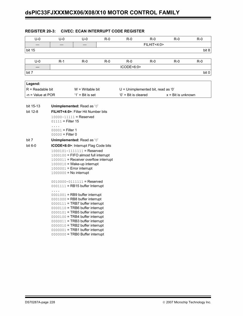
dsPIC33FJXXXMCX06/X08/X10 MOTOR CONTROL FAMILY
REGISTER 20-3: CiVEC: ECAN INTERRUPT CODE REGISTER
U-0 U-0 U-0 R-0 R-0 R-0 R-0 R-0— — — FILHIT<4:0>
bit 15 bit 8
U-0 R-1 R-0 R-0 R-0 R-0 R-0 R-0— ICODE<6:0>
bit 7 bit 0
Legend:R = Readable bit W = Writable bit U = Unimplemented bit, read as ‘0’-n = Value at POR ‘1’ = Bit is set ‘0’ = Bit is cleared x = Bit is unknown
bit 15-13 Unimplemented: Read as ‘0’bit 12-8 FILHIT<4:0>: Filter Hit Number bits
10000-11111 = Reserved01111 = Filter 15....00001 = Filter 100000 = Filter 0
bit 7 Unimplemented: Read as ‘0’bit 6-0 ICODE<6:0>: Interrupt Flag Code bits
1000101-1111111 = Reserved1000100 = FIFO almost full interrupt1000011 = Receiver overflow interrupt1000010 = Wake-up interrupt1000001 = Error interrupt1000000 = No interrupt
0010000-0111111 = Reserved0001111 = RB15 buffer Interrupt ....0001001 = RB9 buffer interrupt 0001000 = RB8 buffer interrupt 0000111 = TRB7 buffer interrupt0000110 = TRB6 buffer interrupt0000101 = TRB5 buffer interrupt0000100 = TRB4 buffer interrupt0000011 = TRB3 buffer interrupt0000010 = TRB2 buffer interrupt0000001 = TRB1 buffer interrupt0000000 = TRB0 Buffer interrupt
DS70287A-page 228 © 2007 Microchip Technology Inc.
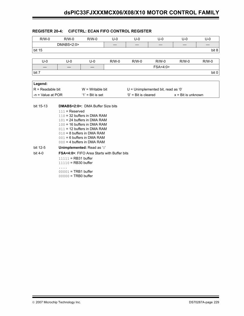
dsPIC33FJXXXMCX06/X08/X10 MOTOR CONTROL FAMILY
REGISTER 20-4: CiFCTRL: ECAN FIFO CONTROL REGISTER
R/W-0 R/W-0 R/W-0 U-0 U-0 U-0 U-0 U-0DMABS<2:0> — — — — —
bit 15 bit 8
U-0 U-0 U-0 R/W-0 R/W-0 R/W-0 R/W-0 R/W-0— — — FSA<4:0>
bit 7 bit 0
Legend:R = Readable bit W = Writable bit U = Unimplemented bit, read as ‘0’-n = Value at POR ‘1’ = Bit is set ‘0’ = Bit is cleared x = Bit is unknown
bit 15-13 DMABS<2:0>: DMA Buffer Size bits 111 = Reserved110 = 32 buffers in DMA RAM101 = 24 buffers in DMA RAM100 = 16 buffers in DMA RAM011 = 12 buffers in DMA RAM010 = 8 buffers in DMA RAM001 = 6 buffers in DMA RAM000 = 4 buffers in DMA RAM
bit 12-5 Unimplemented: Read as ‘0’bit 4-0 FSA<4:0>: FIFO Area Starts with Buffer bits
11111 = RB31 buffer11110 = RB30 buffer....00001 = TRB1 buffer00000 = TRB0 buffer
© 2007 Microchip Technology Inc. DS70287A-page 229
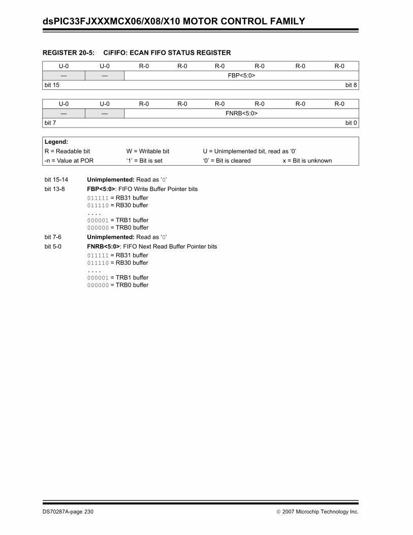
dsPIC33FJXXXMCX06/X08/X10 MOTOR CONTROL FAMILY
REGISTER 20-5: CiFIFO: ECAN FIFO STATUS REGISTER
U-0 U-0 R-0 R-0 R-0 R-0 R-0 R-0— — FBP<5:0>
bit 15 bit 8
U-0 U-0 R-0 R-0 R-0 R-0 R-0 R-0— — FNRB<5:0>
bit 7 bit 0
Legend:R = Readable bit W = Writable bit U = Unimplemented bit, read as ‘0’-n = Value at POR ‘1’ = Bit is set ‘0’ = Bit is cleared x = Bit is unknown
bit 15-14 Unimplemented: Read as ‘0’bit 13-8 FBP<5:0>: FIFO Write Buffer Pointer bits
011111 = RB31 buffer011110 = RB30 buffer....000001 = TRB1 buffer000000 = TRB0 buffer
bit 7-6 Unimplemented: Read as ‘0’bit 5-0 FNRB<5:0>: FIFO Next Read Buffer Pointer bits
011111 = RB31 buffer011110 = RB30 buffer....000001 = TRB1 buffer000000 = TRB0 buffer
DS70287A-page 230 © 2007 Microchip Technology Inc.
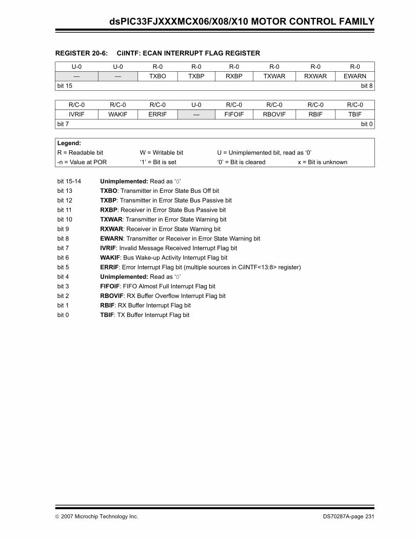
dsPIC33FJXXXMCX06/X08/X10 MOTOR CONTROL FAMILY
REGISTER 20-6: CiINTF: ECAN INTERRUPT FLAG REGISTER
U-0 U-0 R-0 R-0 R-0 R-0 R-0 R-0— — TXBO TXBP RXBP TXWAR RXWAR EWARN
bit 15 bit 8
R/C-0 R/C-0 R/C-0 U-0 R/C-0 R/C-0 R/C-0 R/C-0IVRIF WAKIF ERRIF — FIFOIF RBOVIF RBIF TBIF
bit 7 bit 0
Legend:R = Readable bit W = Writable bit U = Unimplemented bit, read as ‘0’-n = Value at POR ‘1’ = Bit is set ‘0’ = Bit is cleared x = Bit is unknown
bit 15-14 Unimplemented: Read as ‘0’bit 13 TXBO: Transmitter in Error State Bus Off bitbit 12 TXBP: Transmitter in Error State Bus Passive bitbit 11 RXBP: Receiver in Error State Bus Passive bitbit 10 TXWAR: Transmitter in Error State Warning bitbit 9 RXWAR: Receiver in Error State Warning bitbit 8 EWARN: Transmitter or Receiver in Error State Warning bitbit 7 IVRIF: Invalid Message Received Interrupt Flag bitbit 6 WAKIF: Bus Wake-up Activity Interrupt Flag bitbit 5 ERRIF: Error Interrupt Flag bit (multiple sources in CiINTF<13:8> register)bit 4 Unimplemented: Read as ‘0’bit 3 FIFOIF: FIFO Almost Full Interrupt Flag bitbit 2 RBOVIF: RX Buffer Overflow Interrupt Flag bitbit 1 RBIF: RX Buffer Interrupt Flag bitbit 0 TBIF: TX Buffer Interrupt Flag bit
© 2007 Microchip Technology Inc. DS70287A-page 231
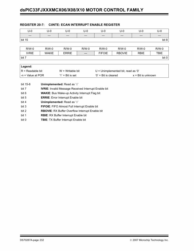
dsPIC33FJXXXMCX06/X08/X10 MOTOR CONTROL FAMILY
REGISTER 20-7: CiINTE: ECAN INTERRUPT ENABLE REGISTER
U-0 U-0 U-0 U-0 U-0 U-0 U-0 U-0— — — — — — — —
bit 15 bit 8
R/W-0 R/W-0 R/W-0 R/W-0 R/W-0 R/W-0 R/W-0 R/W-0IVRIE WAKIE ERRIE — FIFOIE RBOVIE RBIE TBIE
bit 7 bit 0
Legend:R = Readable bit W = Writable bit U = Unimplemented bit, read as ‘0’-n = Value at POR ‘1’ = Bit is set ‘0’ = Bit is cleared x = Bit is unknown
bit 15-8 Unimplemented: Read as ‘0’bit 7 IVRIE: Invalid Message Received Interrupt Enable bitbit 6 WAKIE: Bus Wake-up Activity Interrupt Flag bitbit 5 ERRIE: Error Interrupt Enable bitbit 4 Unimplemented: Read as ‘0’bit 3 FIFOIE: FIFO Almost Full Interrupt Enable bitbit 2 RBOVIE: RX Buffer Overflow Interrupt Enable bitbit 1 RBIE: RX Buffer Interrupt Enable bitbit 0 TBIE: TX Buffer Interrupt Enable bit
DS70287A-page 232 © 2007 Microchip Technology Inc.
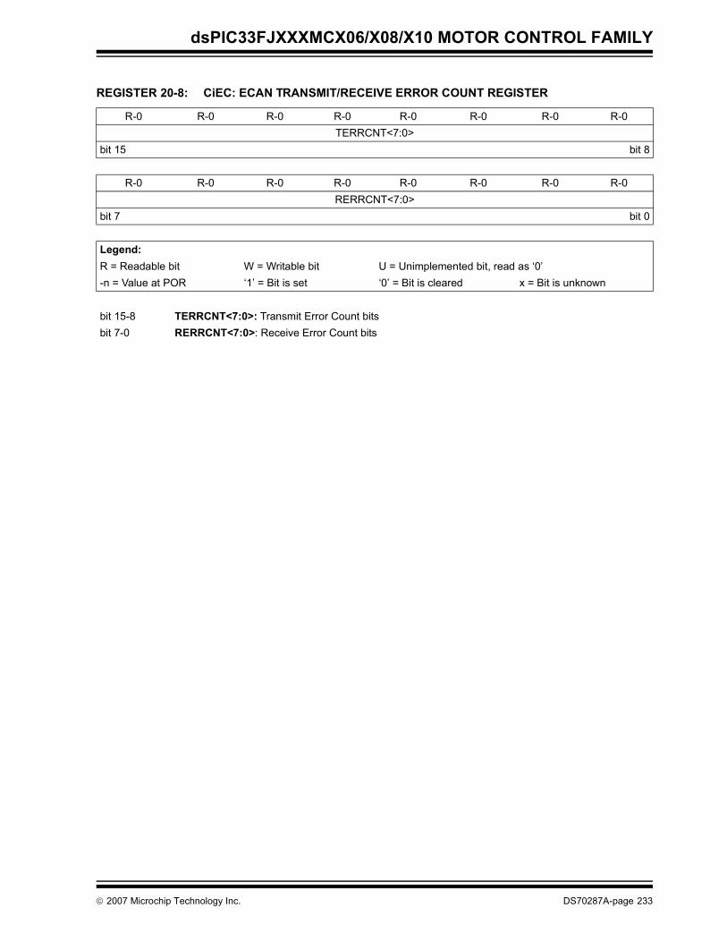
dsPIC33FJXXXMCX06/X08/X10 MOTOR CONTROL FAMILY
REGISTER 20-8: CiEC: ECAN TRANSMIT/RECEIVE ERROR COUNT REGISTER
R-0 R-0 R-0 R-0 R-0 R-0 R-0 R-0TERRCNT<7:0>
bit 15 bit 8
R-0 R-0 R-0 R-0 R-0 R-0 R-0 R-0RERRCNT<7:0>
bit 7 bit 0
Legend:R = Readable bit W = Writable bit U = Unimplemented bit, read as ‘0’-n = Value at POR ‘1’ = Bit is set ‘0’ = Bit is cleared x = Bit is unknown
bit 15-8 TERRCNT<7:0>: Transmit Error Count bitsbit 7-0 RERRCNT<7:0>: Receive Error Count bits
© 2007 Microchip Technology Inc. DS70287A-page 233
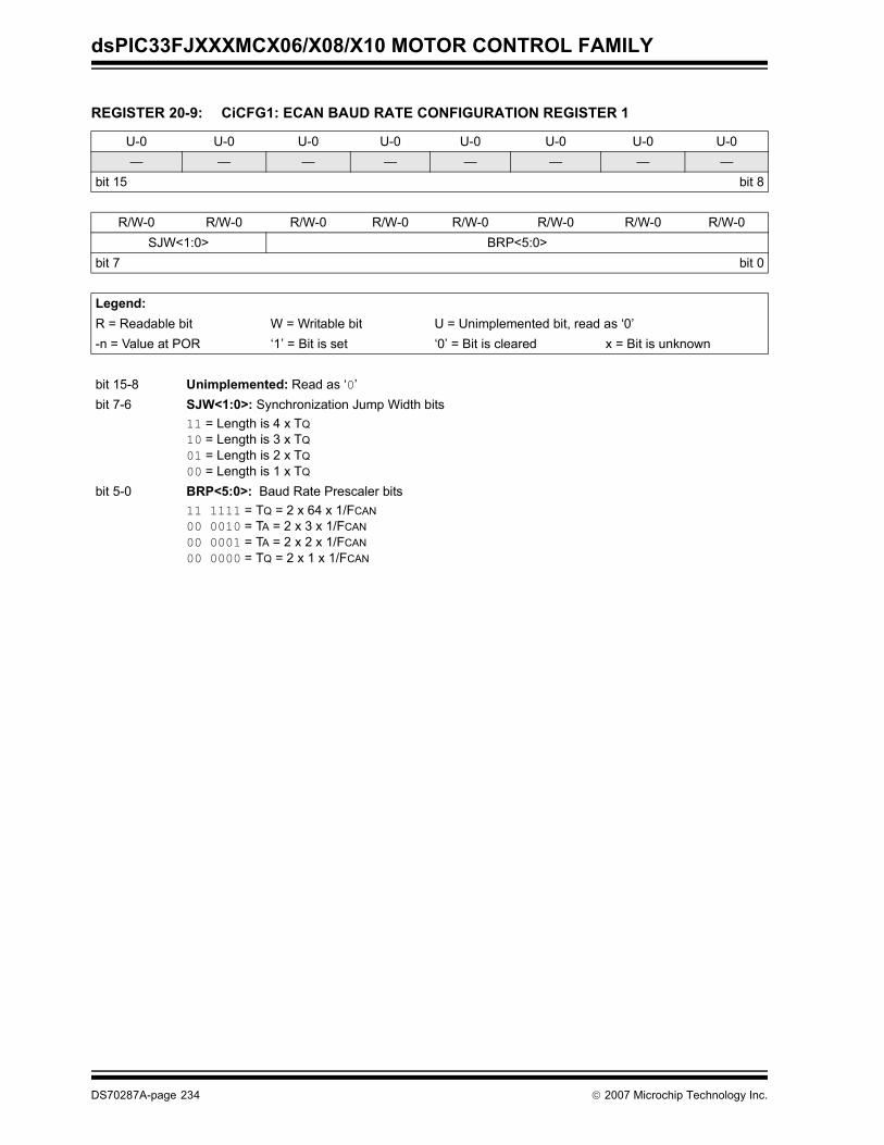
dsPIC33FJXXXMCX06/X08/X10 MOTOR CONTROL FAMILY
REGISTER 20-9: CiCFG1: ECAN BAUD RATE CONFIGURATION REGISTER 1
U-0 U-0 U-0 U-0 U-0 U-0 U-0 U-0— — — — — — — —
bit 15 bit 8
R/W-0 R/W-0 R/W-0 R/W-0 R/W-0 R/W-0 R/W-0 R/W-0SJW<1:0> BRP<5:0>
bit 7 bit 0
Legend:R = Readable bit W = Writable bit U = Unimplemented bit, read as ‘0’-n = Value at POR ‘1’ = Bit is set ‘0’ = Bit is cleared x = Bit is unknown
bit 15-8 Unimplemented: Read as ‘0’bit 7-6 SJW<1:0>: Synchronization Jump Width bits
11 = Length is 4 x TQ 10 = Length is 3 x TQ 01 = Length is 2 x TQ 00 = Length is 1 x TQ
bit 5-0 BRP<5:0>: Baud Rate Prescaler bits11 1111 = TQ = 2 x 64 x 1/FCAN 00 0010 = TA = 2 x 3 x 1/FCAN00 0001 = TA = 2 x 2 x 1/FCAN 00 0000 = TQ = 2 x 1 x 1/FCAN
DS70287A-page 234 © 2007 Microchip Technology Inc.
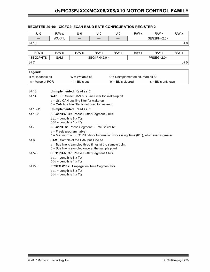
dsPIC33FJXXXMCX06/X08/X10 MOTOR CONTROL FAMILY
REGISTER 20-10: CiCFG2: ECAN BAUD RATE CONFIGURATION REGISTER 2
U-0 R/W-x U-0 U-0 U-0 R/W-x R/W-x R/W-x— WAKFIL — — — SEG2PH<2:0>
bit 15 bit 8
R/W-x R/W-x R/W-x R/W-x R/W-x R/W-x R/W-x R/W-xSEG2PHTS SAM SEG1PH<2:0> PRSEG<2:0>
bit 7 bit 0
Legend:R = Readable bit W = Writable bit U = Unimplemented bit, read as ‘0’-n = Value at POR ‘1’ = Bit is set ‘0’ = Bit is cleared x = Bit is unknown
bit 15 Unimplemented: Read as ‘0’bit 14 WAKFIL: Select CAN bus Line Filter for Wake-up bit
1 = Use CAN bus line filter for wake-up0 = CAN bus line filter is not used for wake-up
bit 13-11 Unimplemented: Read as ‘0’bit 10-8 SEG2PH<2:0>: Phase Buffer Segment 2 bits
111 = Length is 8 x TQ 000 = Length is 1 x TQ
bit 7 SEG2PHTS: Phase Segment 2 Time Select bit1 = Freely programmable0 = Maximum of SEG1PH bits or Information Processing Time (IPT), whichever is greater
bit 6 SAM: Sample of the CAN bus Line bit1 = Bus line is sampled three times at the sample point 0 = Bus line is sampled once at the sample point
bit 5-3 SEG1PH<2:0>: Phase Buffer Segment 1 bits111 = Length is 8 x TQ 000 = Length is 1 x TQ
bit 2-0 PRSEG<2:0>: Propagation Time Segment bits111 = Length is 8 x TQ 000 = Length is 1 x TQ
© 2007 Microchip Technology Inc. DS70287A-page 235
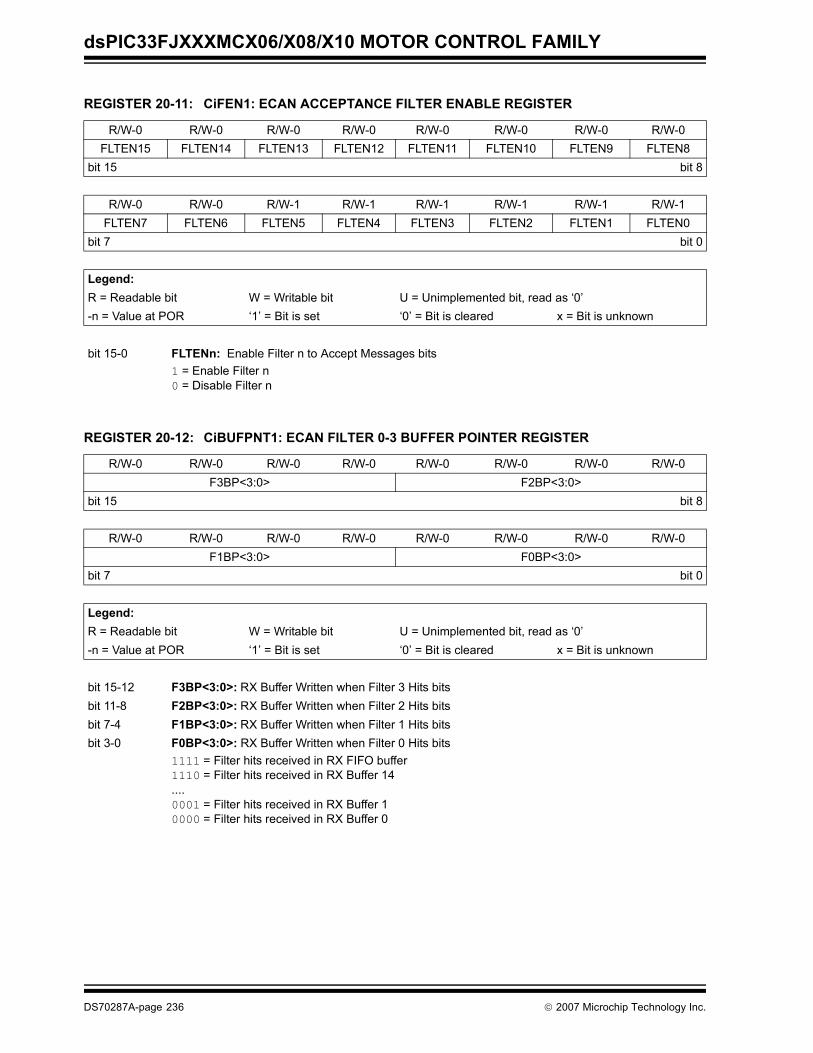
dsPIC33FJXXXMCX06/X08/X10 MOTOR CONTROL FAMILY
REGISTER 20-11: CiFEN1: ECAN ACCEPTANCE FILTER ENABLE REGISTER
R/W-0 R/W-0 R/W-0 R/W-0 R/W-0 R/W-0 R/W-0 R/W-0FLTEN15 FLTEN14 FLTEN13 FLTEN12 FLTEN11 FLTEN10 FLTEN9 FLTEN8
bit 15 bit 8
R/W-0 R/W-0 R/W-1 R/W-1 R/W-1 R/W-1 R/W-1 R/W-1FLTEN7 FLTEN6 FLTEN5 FLTEN4 FLTEN3 FLTEN2 FLTEN1 FLTEN0
bit 7 bit 0
Legend:R = Readable bit W = Writable bit U = Unimplemented bit, read as ‘0’-n = Value at POR ‘1’ = Bit is set ‘0’ = Bit is cleared x = Bit is unknown
bit 15-0 FLTENn: Enable Filter n to Accept Messages bits1 = Enable Filter n0 = Disable Filter n
REGISTER 20-12: CiBUFPNT1: ECAN FILTER 0-3 BUFFER POINTER REGISTER
R/W-0 R/W-0 R/W-0 R/W-0 R/W-0 R/W-0 R/W-0 R/W-0F3BP<3:0> F2BP<3:0>
bit 15 bit 8
R/W-0 R/W-0 R/W-0 R/W-0 R/W-0 R/W-0 R/W-0 R/W-0F1BP<3:0> F0BP<3:0>
bit 7 bit 0
Legend:R = Readable bit W = Writable bit U = Unimplemented bit, read as ‘0’-n = Value at POR ‘1’ = Bit is set ‘0’ = Bit is cleared x = Bit is unknown
bit 15-12 F3BP<3:0>: RX Buffer Written when Filter 3 Hits bitsbit 11-8 F2BP<3:0>: RX Buffer Written when Filter 2 Hits bitsbit 7-4 F1BP<3:0>: RX Buffer Written when Filter 1 Hits bitsbit 3-0 F0BP<3:0>: RX Buffer Written when Filter 0 Hits bits
1111 = Filter hits received in RX FIFO buffer1110 = Filter hits received in RX Buffer 14....0001 = Filter hits received in RX Buffer 10000 = Filter hits received in RX Buffer 0
DS70287A-page 236 © 2007 Microchip Technology Inc.
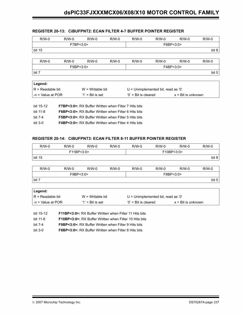
dsPIC33FJXXXMCX06/X08/X10 MOTOR CONTROL FAMILY
REGISTER 20-13: CiBUFPNT2: ECAN FILTER 4-7 BUFFER POINTER REGISTER
R/W-0 R/W-0 R/W-0 R/W-0 R/W-0 R/W-0 R/W-0 R/W-0F7BP<3:0> F6BP<3:0>
bit 15 bit 8
R/W-0 R/W-0 R/W-0 R/W-0 R/W-0 R/W-0 R/W-0 R/W-0F5BP<3:0> F4BP<3:0>
bit 7 bit 0
Legend:R = Readable bit W = Writable bit U = Unimplemented bit, read as ‘0’-n = Value at POR ‘1’ = Bit is set ‘0’ = Bit is cleared x = Bit is unknown
bit 15-12 F7BP<3:0>: RX Buffer Written when Filter 7 Hits bitsbit 11-8 F6BP<3:0>: RX Buffer Written when Filter 6 Hits bitsbit 7-4 F5BP<3:0>: RX Buffer Written when Filter 5 Hits bitsbit 3-0 F4BP<3:0>: RX Buffer Written when Filter 4 Hits bits
REGISTER 20-14: CiBUFPNT3: ECAN FILTER 8-11 BUFFER POINTER REGISTER
R/W-0 R/W-0 R/W-0 R/W-0 R/W-0 R/W-0 R/W-0 R/W-0F11BP<3:0> F10BP<3:0>
bit 15 bit 8
R/W-0 R/W-0 R/W-0 R/W-0 R/W-0 R/W-0 R/W-0 R/W-0F9BP<3:0> F8BP<3:0>
bit 7 bit 0
Legend:R = Readable bit W = Writable bit U = Unimplemented bit, read as ‘0’-n = Value at POR ‘1’ = Bit is set ‘0’ = Bit is cleared x = Bit is unknown
bit 15-12 F11BP<3:0>: RX Buffer Written when Filter 11 Hits bitsbit 11-8 F10BP<3:0>: RX Buffer Written when Filter 10 Hits bitsbit 7-4 F9BP<3:0>: RX Buffer Written when Filter 9 Hits bitsbit 3-0 F8BP<3:0>: RX Buffer Written when Filter 8 Hits bits
© 2007 Microchip Technology Inc. DS70287A-page 237
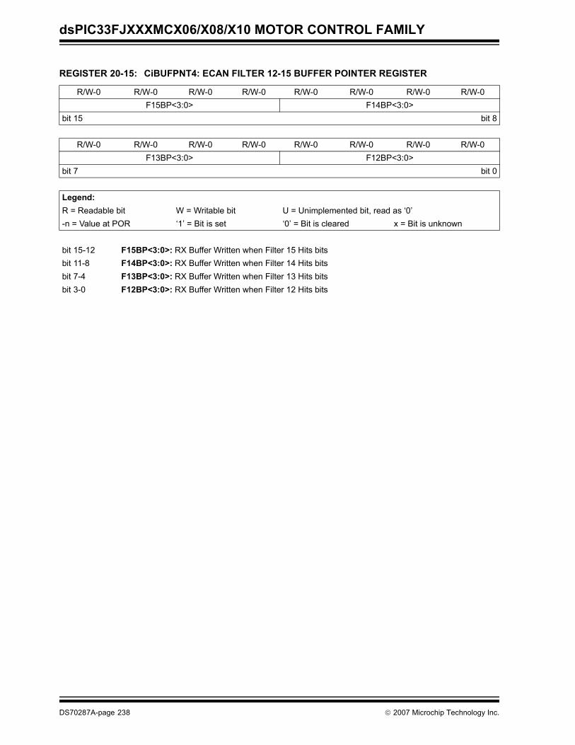
dsPIC33FJXXXMCX06/X08/X10 MOTOR CONTROL FAMILY
REGISTER 20-15: CiBUFPNT4: ECAN FILTER 12-15 BUFFER POINTER REGISTER
R/W-0 R/W-0 R/W-0 R/W-0 R/W-0 R/W-0 R/W-0 R/W-0F15BP<3:0> F14BP<3:0>
bit 15 bit 8
R/W-0 R/W-0 R/W-0 R/W-0 R/W-0 R/W-0 R/W-0 R/W-0F13BP<3:0> F12BP<3:0>
bit 7 bit 0
Legend:R = Readable bit W = Writable bit U = Unimplemented bit, read as ‘0’-n = Value at POR ‘1’ = Bit is set ‘0’ = Bit is cleared x = Bit is unknown
bit 15-12 F15BP<3:0>: RX Buffer Written when Filter 15 Hits bitsbit 11-8 F14BP<3:0>: RX Buffer Written when Filter 14 Hits bitsbit 7-4 F13BP<3:0>: RX Buffer Written when Filter 13 Hits bitsbit 3-0 F12BP<3:0>: RX Buffer Written when Filter 12 Hits bits
DS70287A-page 238 © 2007 Microchip Technology Inc.
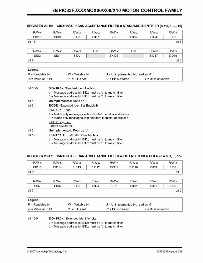
dsPIC33FJXXXMCX06/X08/X10 MOTOR CONTROL FAMILY
REGISTER 20-16: CiRXFnSID: ECAN ACCEPTANCE FILTER n STANDARD IDENTIFIER (n = 0, 1, ..., 15)
R/W-x R/W-x R/W-x R/W-x R/W-x R/W-x R/W-x R/W-xSID10 SID9 SID8 SID7 SID6 SID5 SID4 SID3
bit 15 bit 8
R/W-x R/W-x R/W-x U-0 R/W-x U-0 R/W-x R/W-xSID2 SID1 SID0 — EXIDE — EID17 EID16
bit 7 bit 0
Legend:R = Readable bit W = Writable bit U = Unimplemented bit, read as ‘0’-n = Value at POR ‘1’ = Bit is set ‘0’ = Bit is cleared x = Bit is unknown
bit 15-5 SID<10:0>: Standard Identifier bits1 = Message address bit SIDx must be ‘1’ to match filter0 = Message address bit SIDx must be ‘0’ to match filter
bit 4 Unimplemented: Read as ‘0’bit 3 EXIDE: Extended Identifier Enable bit
If MIDE = 1 then:1 = Match only messages with extended identifier addresses0 = Match only messages with standard identifier addressesIf MIDE = 0 then: Ignore EXIDE bit.
bit 2 Unimplemented: Read as ‘0’bit 1-0 EID<17:16>: Extended Identifier bits
1 = Message address bit EIDx must be ‘1’ to match filter0 = Message address bit EIDx must be ‘0’ to match filter
REGISTER 20-17: CiRXFnEID: ECAN ACCEPTANCE FILTER n EXTENDED IDENTIFIER (n = 0, 1, ..., 15)
R/W-x R/W-x R/W-x R/W-x R/W-x R/W-x R/W-x R/W-xEID15 EID14 EID13 EID12 EID11 EID10 EID9 EID8
bit 15 bit 8
R/W-x R/W-x R/W-x R/W-x R/W-x R/W-x R/W-x R/W-xEID7 EID6 EID5 EID4 EID3 EID2 EID1 EID0
bit 7 bit 0
Legend:R = Readable bit W = Writable bit U = Unimplemented bit, read as ‘0’-n = Value at POR ‘1’ = Bit is set ‘0’ = Bit is cleared x = Bit is unknown
bit 15-0 EID<15:0>: Extended Identifier bits1 = Message address bit EIDx must be ‘1’ to match filter0 = Message address bit EIDx must be ‘0’ to match filter
© 2007 Microchip Technology Inc. DS70287A-page 239
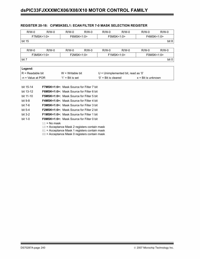
dsPIC33FJXXXMCX06/X08/X10 MOTOR CONTROL FAMILY
REGISTER 20-18: CiFMSKSEL1: ECAN FILTER 7-0 MASK SELECTION REGISTER
R/W-0 R/W-0 R/W-0 R/W-0 R/W-0 R/W-0 R/W-0 R/W-0F7MSK<1:0> F6MSK<1:0> F5MSK<1:0> F4MSK<1:0>
bit 15 bit 8
R/W-0 R/W-0 R/W-0 R/W-0 R/W-0 R/W-0 R/W-0 R/W-0F3MSK<1:0> F2MSK<1:0> F1MSK<1:0> F0MSK<1:0>
bit 7 bit 0
Legend:R = Readable bit W = Writable bit U = Unimplemented bit, read as ‘0’-n = Value at POR ‘1’ = Bit is set ‘0’ = Bit is cleared x = Bit is unknown
bit 15-14 F7MSK<1:0>: Mask Source for Filter 7 bitbit 13-12 F6MSK<1:0>: Mask Source for Filter 6 bitbit 11-10 F5MSK<1:0>: Mask Source for Filter 5 bitbit 9-8 F4MSK<1:0>: Mask Source for Filter 4 bitbit 7-6 F3MSK<1:0>: Mask Source for Filter 3 bitbit 5-4 F2MSK<1:0>: Mask Source for Filter 2 bitbit 3-2 F1MSK<1:0>: Mask Source for Filter 1 bitbit 1-0 F0MSK<1:0>: Mask Source for Filter 0 bit
11 = No mask10 = Acceptance Mask 2 registers contain mask01 = Acceptance Mask 1 registers contain mask00 = Acceptance Mask 0 registers contain mask
DS70287A-page 240 © 2007 Microchip Technology Inc.
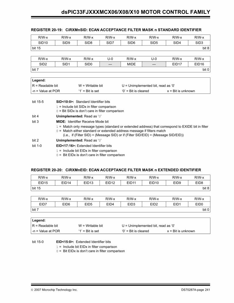
dsPIC33FJXXXMCX06/X08/X10 MOTOR CONTROL FAMILY
REGISTER 20-19: CiRXMnSID: ECAN ACCEPTANCE FILTER MASK n STANDARD IDENTIFIER
R/W-x R/W-x R/W-x R/W-x R/W-x R/W-x R/W-x R/W-xSID10 SID9 SID8 SID7 SID6 SID5 SID4 SID3
bit 15 bit 8
R/W-x R/W-x R/W-x U-0 R/W-x U-0 R/W-x R/W-xSID2 SID1 SID0 — MIDE — EID17 EID16
bit 7 bit 0
Legend:R = Readable bit W = Writable bit U = Unimplemented bit, read as ‘0’-n = Value at POR ‘1’ = Bit is set ‘0’ = Bit is cleared x = Bit is unknown
bit 15-5 SID<10:0>: Standard Identifier bits1 = Include bit SIDx in filter comparison0 = Bit SIDx is don’t care in filter comparison
bit 4 Unimplemented: Read as ‘0’bit 3 MIDE: Identifier Receive Mode bit
1 = Match only message types (standard or extended address) that correspond to EXIDE bit in filter 0 = Match either standard or extended address message if filters match
(i.e., if (Filter SID) = (Message SID) or if (Filter SID/EID) = (Message SID/EID))bit 2 Unimplemented: Read as ‘0’bit 1-0 EID<17:16>: Extended Identifier bits
1 = Include bit EIDx in filter comparison0 = Bit EIDx is don’t care in filter comparison
REGISTER 20-20: CiRXMnEID: ECAN ACCEPTANCE FILTER MASK n EXTENDED IDENTIFIER
R/W-x R/W-x R/W-x R/W-x R/W-x R/W-x R/W-x R/W-xEID15 EID14 EID13 EID12 EID11 EID10 EID9 EID8
bit 15 bit 8
R/W-x R/W-x R/W-x R/W-x R/W-x R/W-x R/W-x R/W-xEID7 EID6 EID5 EID4 EID3 EID2 EID1 EID0
bit 7 bit 0
Legend:R = Readable bit W = Writable bit U = Unimplemented bit, read as ‘0’-n = Value at POR ‘1’ = Bit is set ‘0’ = Bit is cleared x = Bit is unknown
bit 15-0 EID<15:0>: Extended Identifier bits1 = Include bit EIDx in filter comparison0 = Bit EIDx is don’t care in filter comparison
© 2007 Microchip Technology Inc. DS70287A-page 241
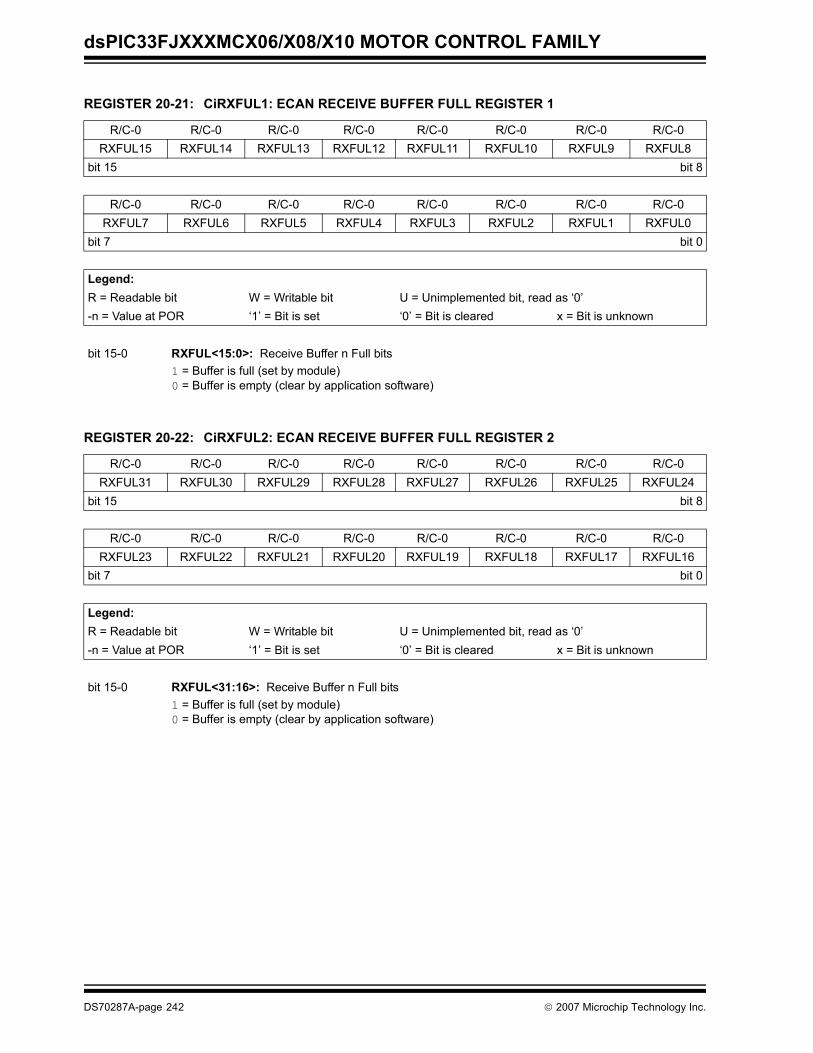
dsPIC33FJXXXMCX06/X08/X10 MOTOR CONTROL FAMILY
REGISTER 20-21: CiRXFUL1: ECAN RECEIVE BUFFER FULL REGISTER 1
R/C-0 R/C-0 R/C-0 R/C-0 R/C-0 R/C-0 R/C-0 R/C-0RXFUL15 RXFUL14 RXFUL13 RXFUL12 RXFUL11 RXFUL10 RXFUL9 RXFUL8
bit 15 bit 8
R/C-0 R/C-0 R/C-0 R/C-0 R/C-0 R/C-0 R/C-0 R/C-0RXFUL7 RXFUL6 RXFUL5 RXFUL4 RXFUL3 RXFUL2 RXFUL1 RXFUL0
bit 7 bit 0
Legend:R = Readable bit W = Writable bit U = Unimplemented bit, read as ‘0’-n = Value at POR ‘1’ = Bit is set ‘0’ = Bit is cleared x = Bit is unknown
bit 15-0 RXFUL<15:0>: Receive Buffer n Full bits1 = Buffer is full (set by module) 0 = Buffer is empty (clear by application software)
REGISTER 20-22: CiRXFUL2: ECAN RECEIVE BUFFER FULL REGISTER 2
R/C-0 R/C-0 R/C-0 R/C-0 R/C-0 R/C-0 R/C-0 R/C-0RXFUL31 RXFUL30 RXFUL29 RXFUL28 RXFUL27 RXFUL26 RXFUL25 RXFUL24
bit 15 bit 8
R/C-0 R/C-0 R/C-0 R/C-0 R/C-0 R/C-0 R/C-0 R/C-0RXFUL23 RXFUL22 RXFUL21 RXFUL20 RXFUL19 RXFUL18 RXFUL17 RXFUL16
bit 7 bit 0
Legend:R = Readable bit W = Writable bit U = Unimplemented bit, read as ‘0’-n = Value at POR ‘1’ = Bit is set ‘0’ = Bit is cleared x = Bit is unknown
bit 15-0 RXFUL<31:16>: Receive Buffer n Full bits1 = Buffer is full (set by module) 0 = Buffer is empty (clear by application software)
DS70287A-page 242 © 2007 Microchip Technology Inc.
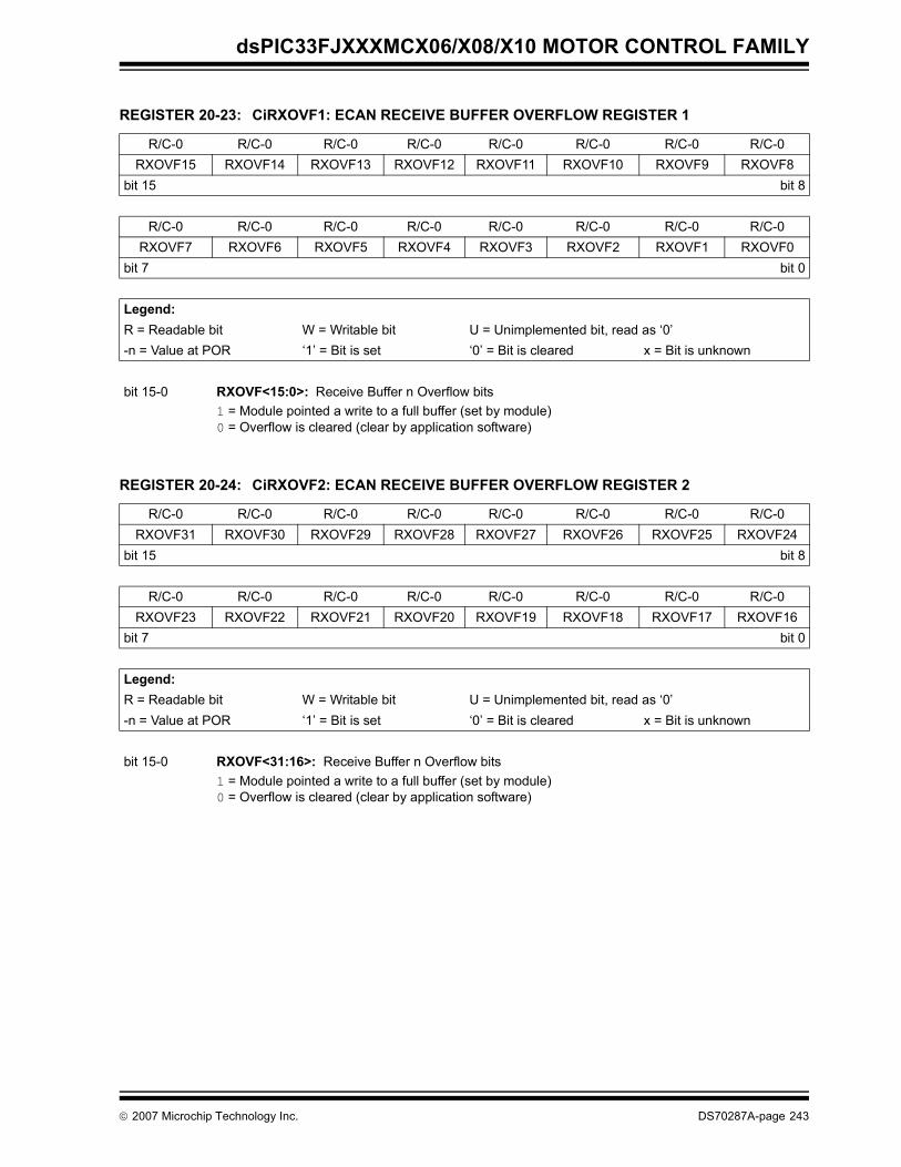
dsPIC33FJXXXMCX06/X08/X10 MOTOR CONTROL FAMILY
REGISTER 20-23: CiRXOVF1: ECAN RECEIVE BUFFER OVERFLOW REGISTER 1
R/C-0 R/C-0 R/C-0 R/C-0 R/C-0 R/C-0 R/C-0 R/C-0RXOVF15 RXOVF14 RXOVF13 RXOVF12 RXOVF11 RXOVF10 RXOVF9 RXOVF8
bit 15 bit 8
R/C-0 R/C-0 R/C-0 R/C-0 R/C-0 R/C-0 R/C-0 R/C-0RXOVF7 RXOVF6 RXOVF5 RXOVF4 RXOVF3 RXOVF2 RXOVF1 RXOVF0
bit 7 bit 0
Legend:R = Readable bit W = Writable bit U = Unimplemented bit, read as ‘0’-n = Value at POR ‘1’ = Bit is set ‘0’ = Bit is cleared x = Bit is unknown
bit 15-0 RXOVF<15:0>: Receive Buffer n Overflow bits1 = Module pointed a write to a full buffer (set by module) 0 = Overflow is cleared (clear by application software)
REGISTER 20-24: CiRXOVF2: ECAN RECEIVE BUFFER OVERFLOW REGISTER 2
R/C-0 R/C-0 R/C-0 R/C-0 R/C-0 R/C-0 R/C-0 R/C-0RXOVF31 RXOVF30 RXOVF29 RXOVF28 RXOVF27 RXOVF26 RXOVF25 RXOVF24
bit 15 bit 8
R/C-0 R/C-0 R/C-0 R/C-0 R/C-0 R/C-0 R/C-0 R/C-0RXOVF23 RXOVF22 RXOVF21 RXOVF20 RXOVF19 RXOVF18 RXOVF17 RXOVF16
bit 7 bit 0
Legend:R = Readable bit W = Writable bit U = Unimplemented bit, read as ‘0’-n = Value at POR ‘1’ = Bit is set ‘0’ = Bit is cleared x = Bit is unknown
bit 15-0 RXOVF<31:16>: Receive Buffer n Overflow bits1 = Module pointed a write to a full buffer (set by module) 0 = Overflow is cleared (clear by application software)
© 2007 Microchip Technology Inc. DS70287A-page 243

dsPIC33FJXXXMCX06/X08/X10 MOTOR CONTROL FAMILY
REGISTER 20-25: CiTRmnCON: ECAN TX/RX BUFFER m CONTROL REGISTER (m = 0,2,4,6; n = 1,3,5,7)
R/W-0 R-0 R-0 R-0 R/W-0 R/W-0 R/W-0 R/W-0TXENn TXABTn TXLARBn TXERRn TXREQn RTRENn TXnPRI<1:0>
bit 15 bit 8
R/W-0 R-0 R-0 R-0 R/W-0 R/W-0 R/W-0 R/W-0TXENm TXABTm(1) TXLARBm(1) TXERRm(1) TXREQm RTRENm TXmPRI<1:0>
bit 7 bit 0
Legend:R = Readable bit W = Writable bit U = Unimplemented bit, read as ‘0’-n = Value at POR ‘1’ = Bit is set ‘0’ = Bit is cleared x = Bit is unknown
bit 15-8 See Definition for Bits 7-0, Controls Buffer nbit 7 TXENm: TX/RX Buffer Selection bit
1 = Buffer TRBn is a transmit buffer0 = Buffer TRBn is a receive buffer
bit 6 TXABTm: Message Aborted bit(1)
1 = Message was aborted0 = Message completed transmission successfully
bit 5 TXLARBm: Message Lost Arbitration bit(1)
1 = Message lost arbitration while being sent0 = Message did not lose arbitration while being sent
bit 4 TXERRm: Error Detected During Transmission bit(1)
1 = A bus error occurred while the message was being sent0 = A bus error did not occur while the message was being sent
bit 3 TXREQm: Message Send Request bitSetting this bit to ‘1’ requests sending a message. The bit will automatically clear when the messageis successfully sent. Clearing the bit to ‘0’ while set will request a message abort.
bit 2 RTRENm: Auto-Remote Transmit Enable bit 1 = When a remote transmit is received, TXREQ will be set0 = When a remote transmit is received, TXREQ will be unaffected
bit 1-0 TXmPRI<1:0>: Message Transmission Priority bits11 = Highest message priority10 = High intermediate message priority01 = Low intermediate message priority00 = Lowest message priority
Note 1: This bit is cleared when TXREQ is set.
DS70287A-page 244 © 2007 Microchip Technology Inc.
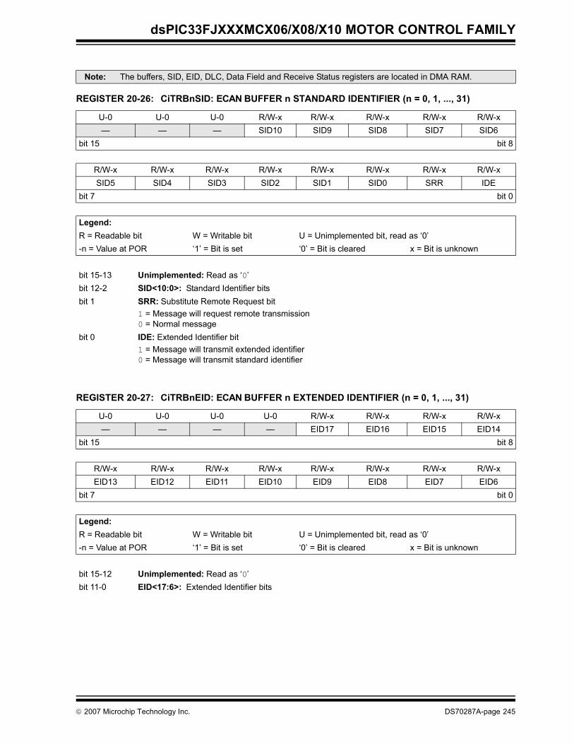
dsPIC33FJXXXMCX06/X08/X10 MOTOR CONTROL FAMILY
Note: The buffers, SID, EID, DLC, Data Field and Receive Status registers are located in DMA RAM.
REGISTER 20-26: CiTRBnSID: ECAN BUFFER n STANDARD IDENTIFIER (n = 0, 1, ..., 31)
U-0 U-0 U-0 R/W-x R/W-x R/W-x R/W-x R/W-x— — — SID10 SID9 SID8 SID7 SID6
bit 15 bit 8
R/W-x R/W-x R/W-x R/W-x R/W-x R/W-x R/W-x R/W-xSID5 SID4 SID3 SID2 SID1 SID0 SRR IDE
bit 7 bit 0
Legend:R = Readable bit W = Writable bit U = Unimplemented bit, read as ‘0’-n = Value at POR ‘1’ = Bit is set ‘0’ = Bit is cleared x = Bit is unknown
bit 15-13 Unimplemented: Read as ‘0’bit 12-2 SID<10:0>: Standard Identifier bitsbit 1 SRR: Substitute Remote Request bit
1 = Message will request remote transmission 0 = Normal message
bit 0 IDE: Extended Identifier bit1 = Message will transmit extended identifier 0 = Message will transmit standard identifier
REGISTER 20-27: CiTRBnEID: ECAN BUFFER n EXTENDED IDENTIFIER (n = 0, 1, ..., 31)
U-0 U-0 U-0 U-0 R/W-x R/W-x R/W-x R/W-x— — — — EID17 EID16 EID15 EID14
bit 15 bit 8
R/W-x R/W-x R/W-x R/W-x R/W-x R/W-x R/W-x R/W-xEID13 EID12 EID11 EID10 EID9 EID8 EID7 EID6
bit 7 bit 0
Legend:R = Readable bit W = Writable bit U = Unimplemented bit, read as ‘0’-n = Value at POR ‘1’ = Bit is set ‘0’ = Bit is cleared x = Bit is unknown
bit 15-12 Unimplemented: Read as ‘0’bit 11-0 EID<17:6>: Extended Identifier bits
© 2007 Microchip Technology Inc. DS70287A-page 245
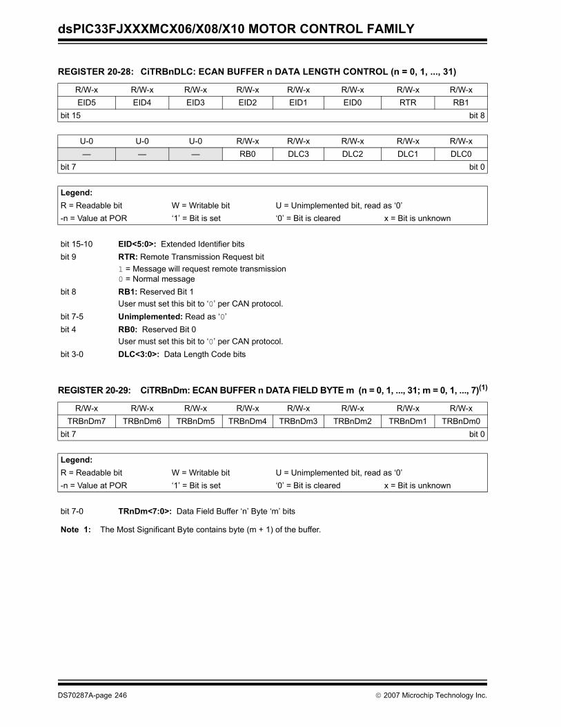
dsPIC33FJXXXMCX06/X08/X10 MOTOR CONTROL FAMILY
REGISTER 20-28: CiTRBnDLC: ECAN BUFFER n DATA LENGTH CONTROL (n = 0, 1, ..., 31)
R/W-x R/W-x R/W-x R/W-x R/W-x R/W-x R/W-x R/W-xEID5 EID4 EID3 EID2 EID1 EID0 RTR RB1
bit 15 bit 8
U-0 U-0 U-0 R/W-x R/W-x R/W-x R/W-x R/W-x— — — RB0 DLC3 DLC2 DLC1 DLC0
bit 7 bit 0
Legend:R = Readable bit W = Writable bit U = Unimplemented bit, read as ‘0’-n = Value at POR ‘1’ = Bit is set ‘0’ = Bit is cleared x = Bit is unknown
bit 15-10 EID<5:0>: Extended Identifier bitsbit 9 RTR: Remote Transmission Request bit
1 = Message will request remote transmission 0 = Normal message
bit 8 RB1: Reserved Bit 1User must set this bit to ‘0’ per CAN protocol.
bit 7-5 Unimplemented: Read as ‘0’bit 4 RB0: Reserved Bit 0
User must set this bit to ‘0’ per CAN protocol.bit 3-0 DLC<3:0>: Data Length Code bits
REGISTER 20-29: CiTRBnDm: ECAN BUFFER n DATA FIELD BYTE m (n = 0, 1, ..., 31; m = 0, 1, ..., 7)(1)
R/W-x R/W-x R/W-x R/W-x R/W-x R/W-x R/W-x R/W-xTRBnDm7 TRBnDm6 TRBnDm5 TRBnDm4 TRBnDm3 TRBnDm2 TRBnDm1 TRBnDm0
bit 7 bit 0
Legend:R = Readable bit W = Writable bit U = Unimplemented bit, read as ‘0’-n = Value at POR ‘1’ = Bit is set ‘0’ = Bit is cleared x = Bit is unknown
bit 7-0 TRnDm<7:0>: Data Field Buffer ‘n’ Byte ‘m’ bits
Note 1: The Most Significant Byte contains byte (m + 1) of the buffer.
DS70287A-page 246 © 2007 Microchip Technology Inc.
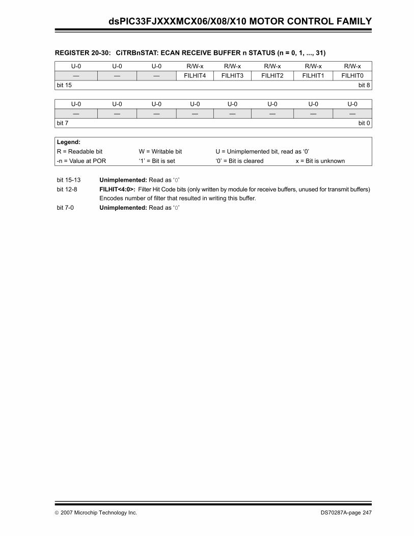
dsPIC33FJXXXMCX06/X08/X10 MOTOR CONTROL FAMILY
REGISTER 20-30: CiTRBnSTAT: ECAN RECEIVE BUFFER n STATUS (n = 0, 1, ..., 31)
U-0 U-0 U-0 R/W-x R/W-x R/W-x R/W-x R/W-x— — — FILHIT4 FILHIT3 FILHIT2 FILHIT1 FILHIT0
bit 15 bit 8
U-0 U-0 U-0 U-0 U-0 U-0 U-0 U-0— — — — — — — —
bit 7 bit 0
Legend:R = Readable bit W = Writable bit U = Unimplemented bit, read as ‘0’-n = Value at POR ‘1’ = Bit is set ‘0’ = Bit is cleared x = Bit is unknown
bit 15-13 Unimplemented: Read as ‘0’bit 12-8 FILHIT<4:0>: Filter Hit Code bits (only written by module for receive buffers, unused for transmit buffers)
Encodes number of filter that resulted in writing this buffer. bit 7-0 Unimplemented: Read as ‘0’
© 2007 Microchip Technology Inc. DS70287A-page 247

dsPIC33FJXXXMCX06/X08/X10 MOTOR CONTROL FAMILY
NOTES:
DS70287A-page 248 © 2007 Microchip Technology Inc.
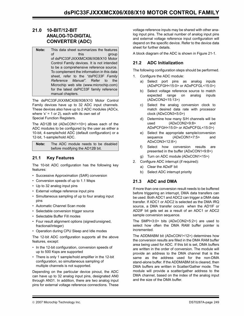
dsPIC33FJXXXMCX06/X08/X10 MOTOR CONTROL FAMILY
21.0 10-BIT/12-BIT ANALOG-TO-DIGITAL CONVERTER (ADC)
The dsPIC33FJXXXMCX06/X08/X10 Motor ControlFamily devices have up to 32 ADC input channels.These devices also have up to 2 ADC modules (ADCx,where ‘x’ = 1 or 2), each with its own set of Special Function Registers.
The AD12B bit (ADxCON1<10>) allows each of theADC modules to be configured by the user as either a10-bit, 4-sample/hold ADC (default configuration) or a12-bit, 1-sample/hold ADC.
21.1 Key FeaturesThe 10-bit ADC configuration has the following keyfeatures:
• Successive Approximation (SAR) conversion• Conversion speeds of up to 1.1 Msps• Up to 32 analog input pins• External voltage reference input pins• Simultaneous sampling of up to four analog input
pins• Automatic Channel Scan mode• Selectable conversion trigger source• Selectable Buffer Fill modes• Four result alignment options (signed/unsigned,
fractional/integer)• Operation during CPU Sleep and Idle modes
The 12-bit ADC configuration supports all the abovefeatures, except:
• In the 12-bit configuration, conversion speeds of up to 500 Ksps are supported
• There is only 1 sample/hold amplifier in the 12-bit configuration, so simultaneous sampling of multiple channels is not supported.
Depending on the particular device pinout, the ADCcan have up to 32 analog input pins, designated AN0through AN31. In addition, there are two analog inputpins for external voltage reference connections. These
voltage reference inputs may be shared with other ana-log input pins. The actual number of analog input pinsand external voltage reference input configuration willdepend on the specific device. Refer to the device datasheet for further details.
A block diagram of the ADC is shown in Figure 21-1.
21.2 ADC InitializationThe following configuration steps should be performed.
1. Configure the ADC module:a) Select port pins as analog inputs
(ADxPCFGH<15:0> or ADxPCFGL<15:0>)b) Select voltage reference source to match
expected range on analog inputs(ADxCON2<15:13>)
c) Select the analog conversion clock tomatch desired data rate with processorclock (ADxCON3<5:0>)
d) Determine how many S/H channels will beused (ADxCON2<9:8> andADxPCFGH<15:0> or ADxPCFGL<15:0>)
e) Select the appropriate sample/conversionsequence (ADxCON1<7:5> andADxCON3<12:8>)
f) Select how conversion results arepresented in the buffer (ADxCON1<9:8>)
g) Turn on ADC module (ADxCON1<15>)2. Configure ADC interrupt (if required):
a) Clear the ADxIF bit b) Select ADC interrupt priority
21.3 ADC and DMAIf more than one conversion result needs to be bufferedbefore triggering an interrupt, DMA data transfers canbe used. Both ADC1 and ADC2 can trigger a DMA datatransfer. If ADC1 or ADC2 is selected as the DMA IRQsource, a DMA transfer occurs when the AD1IF orAD2IF bit gets set as a result of an ADC1 or ADC2sample conversion sequence.
The SMPI<3:0> bits (ADxCON2<5:2>) are used toselect how often the DMA RAM buffer pointer isincremented.
The ADDMABM bit (ADxCON1<12>) determines howthe conversion results are filled in the DMA RAM bufferarea being used for ADC. If this bit is set, DMA buffersare written in the order of conversion. The module willprovide an address to the DMA channel that is thesame as the address used for the non-DMAstand-alone buffer. If the ADDMABM bit is cleared, thenDMA buffers are written in Scatter/Gather mode. Themodule will provide a scatter/gather address to theDMA channel, based on the index of the analog inputand the size of the DMA buffer.
Note: This data sheet summarizes the featuresof this groupof dsPIC33FJXXXMCX06/X08/X10 MotorControl Family devices. It is not intendedto be a comprehensive reference source.To complement the information in this datasheet, refer to the “dsPIC33F FamilyReference Manual”. Refer to theMicrochip web site (www.microchip.com)for the latest dsPIC33F family referencemanual chapters.
Note: The ADC module needs to be disabledbefore modifying the AD12B bit.
© 2007 Microchip Technology Inc. DS70287A-page 249
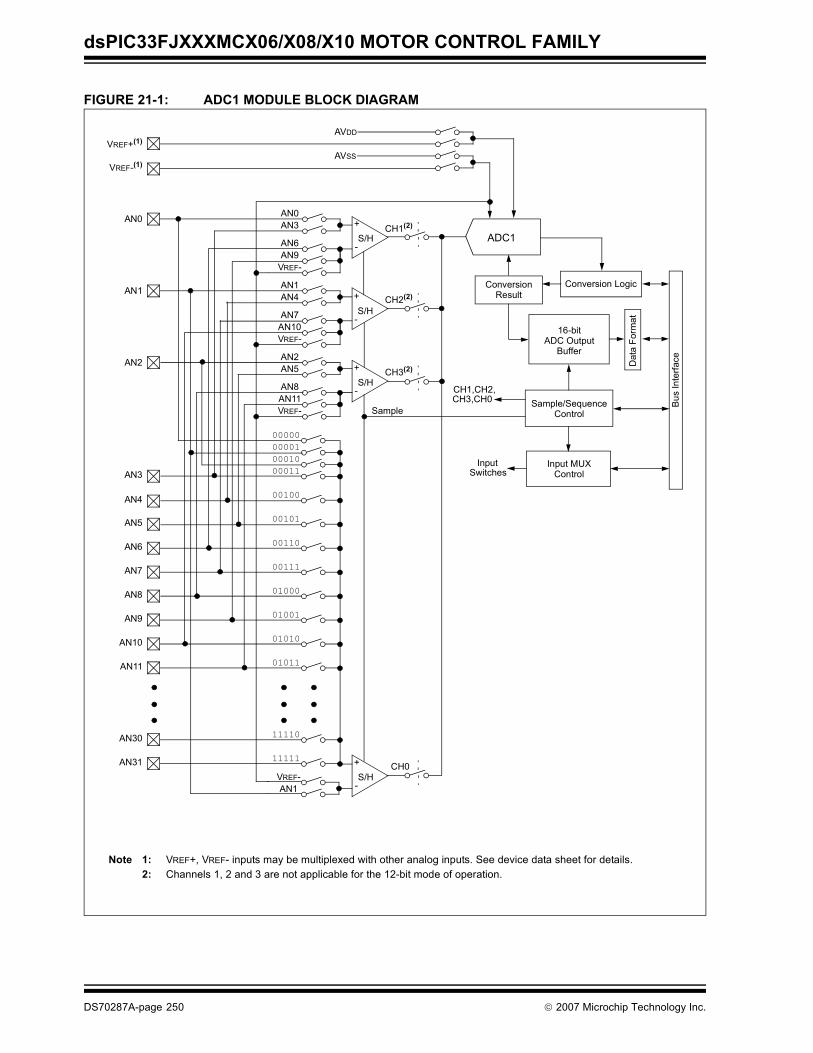
dsPIC33FJXXXMCX06/X08/X10 MOTOR CONTROL FAMILY
FIGURE 21-1: ADC1 MODULE BLOCK DIAGRAM
S/H+
-
Conversion Conversion Logic
VREF+(1)
AVSS
AVDD
ADC1
Dat
a Fo
rmat
16-bitADC Output
Bus
Inte
rface
00000
00101
00111
01001
11110
11111
000010001000011
00100
00110
01000
01010
01011
AN30
AN31
AN8
AN9
AN10
AN11
AN2
AN4
AN7
AN0
AN3
AN1
AN5
CH1(2)
CH2(2)
CH3(2)
CH0
AN5AN2
AN11AN8
VREF-
AN4AN1
AN10AN7
VREF-
AN3AN0
AN9AN6
VREF-
AN1VREF-
VREF-(1)
Sample/SequenceControlSample
CH1,CH2,CH3,CH0
Input MUXControl
InputSwitches
S/H+
-
S/H+
-
S/H+
-
AN6
Buffer
Result
Note 1: VREF+, VREF- inputs may be multiplexed with other analog inputs. See device data sheet for details.2: Channels 1, 2 and 3 are not applicable for the 12-bit mode of operation.
DS70287A-page 250 © 2007 Microchip Technology Inc.
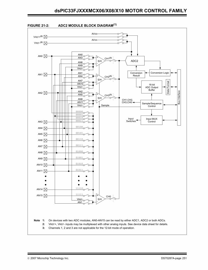
dsPIC33FJXXXMCX06/X08/X10 MOTOR CONTROL FAMILY
FIGURE 21-2: ADC2 MODULE BLOCK DIAGRAM(1)
S/H+
-
Conversion Conversion Logic
VREF+(2)
AVSS
AVDD
ADC2
Dat
a Fo
rmat
16-bitADC Output
Bus
Inte
rface
00000
00101
00111
01001
11110
11111
000010001000011
00100
00110
01000
01010
01011
AN14
AN15
AN8
AN9
AN10
AN11
AN2
AN4
AN7
AN0
AN3
AN1
AN5
CH1(3)
CH2(3)
CH3(3)
CH0
AN5AN2
AN11AN8
VREF-
AN4AN1
AN10AN7
VREF-
AN3AN0
AN9AN6
VREF-
AN1VREF-
VREF-(2)
Sample/SequenceControlSample
CH1,CH2,CH3,CH0
Input MUXControl
InputSwitches
S/H+
-
S/H+
-
S/H+
-
AN6
Buffer
Result
Note 1: On devices with two ADC modules, AN0-AN15 can be read by either ADC1, ADC2 or both ADCs.2: VREF+, VREF- inputs may be multiplexed with other analog inputs. See device data sheet for details.3: Channels 1, 2 and 3 are not applicable for the 12-bit mode of operation.
© 2007 Microchip Technology Inc. DS70287A-page 251
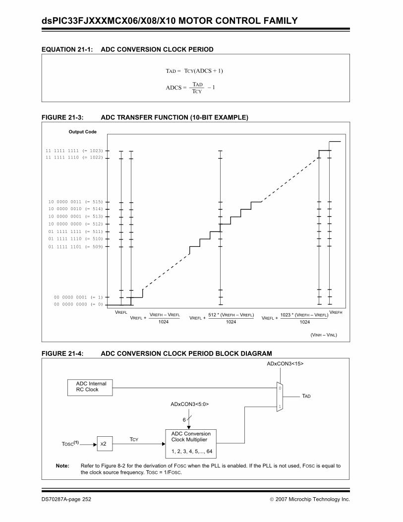
dsPIC33FJXXXMCX06/X08/X10 MOTOR CONTROL FAMILY
EQUATION 21-1: ADC CONVERSION CLOCK PERIOD
FIGURE 21-3: ADC TRANSFER FUNCTION (10-BIT EXAMPLE)
FIGURE 21-4: ADC CONVERSION CLOCK PERIOD BLOCK DIAGRAM
TAD = TCY(ADCS + 1)
ADCS = TADTCY
– 1
10 0000 0010 (= 514)
10 0000 0011 (= 515)
01 1111 1101 (= 509)
01 1111 1110 (= 510)
01 1111 1111 (= 511)
11 1111 1110 (= 1022)
11 1111 1111 (= 1023)
00 0000 0000 (= 0)
00 0000 0001 (= 1)
Output Code
10 0000 0000 (= 512)
(VINH – VINL)
VREFL VREFH – VREFL
1024
VREFHVREFL +
10 0000 0001 (= 513)
512 * (VREFH – VREFL)1024
VREFL + 1023 * (VREFH – VREFL)1024
VREFL +
0
1
ADC Internal RC Clock
TOSC(1) X2
ADC Conversion Clock Multiplier
1, 2, 3, 4, 5,..., 64
ADxCON3<15>
TCY
TAD
6
ADxCON3<5:0>
Note: Refer to Figure 8-2 for the derivation of FOSC when the PLL is enabled. If the PLL is not used, FOSC is equal tothe clock source frequency. TOSC = 1/FOSC.
DS70287A-page 252 © 2007 Microchip Technology Inc.
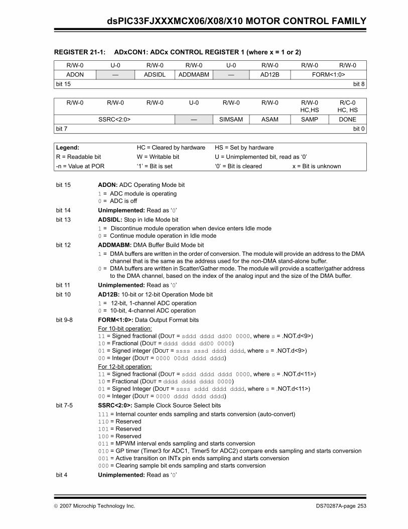
dsPIC33FJXXXMCX06/X08/X10 MOTOR CONTROL FAMILY
REGISTER 21-1: ADxCON1: ADCx CONTROL REGISTER 1 (where x = 1 or 2)
R/W-0 U-0 R/W-0 R/W-0 U-0 R/W-0 R/W-0 R/W-0ADON — ADSIDL ADDMABM — AD12B FORM<1:0>
bit 15 bit 8
R/W-0 R/W-0 R/W-0 U-0 R/W-0 R/W-0 R/W-0HC,HS
R/C-0HC, HS
SSRC<2:0> — SIMSAM ASAM SAMP DONEbit 7 bit 0
Legend: HC = Cleared by hardware HS = Set by hardwareR = Readable bit W = Writable bit U = Unimplemented bit, read as ‘0’-n = Value at POR ‘1’ = Bit is set ‘0’ = Bit is cleared x = Bit is unknown
bit 15 ADON: ADC Operating Mode bit1 = ADC module is operating0 = ADC is off
bit 14 Unimplemented: Read as ‘0’bit 13 ADSIDL: Stop in Idle Mode bit
1 = Discontinue module operation when device enters Idle mode0 = Continue module operation in Idle mode
bit 12 ADDMABM: DMA Buffer Build Mode bit1 = DMA buffers are written in the order of conversion. The module will provide an address to the DMA
channel that is the same as the address used for the non-DMA stand-alone buffer.0 = DMA buffers are written in Scatter/Gather mode. The module will provide a scatter/gather address
to the DMA channel, based on the index of the analog input and the size of the DMA buffer.bit 11 Unimplemented: Read as ‘0’bit 10 AD12B: 10-bit or 12-bit Operation Mode bit
1 = 12-bit, 1-channel ADC operation0 = 10-bit, 4-channel ADC operation
bit 9-8 FORM<1:0>: Data Output Format bitsFor 10-bit operation:11 = Signed fractional (DOUT = sddd dddd dd00 0000, where s = .NOT.d<9>)10 = Fractional (DOUT = dddd dddd dd00 0000)01 = Signed integer (DOUT = ssss sssd dddd dddd, where s = .NOT.d<9>)00 = Integer (DOUT = 0000 00dd dddd dddd)For 12-bit operation:11 = Signed fractional (DOUT = sddd dddd dddd 0000, where s = .NOT.d<11>)10 = Fractional (DOUT = dddd dddd dddd 0000)01 = Signed Integer (DOUT = ssss sddd dddd dddd, where s = .NOT.d<11>)00 = Integer (DOUT = 0000 dddd dddd dddd)
bit 7-5 SSRC<2:0>: Sample Clock Source Select bits111 = Internal counter ends sampling and starts conversion (auto-convert)110 = Reserved101 = Reserved100 = Reserved011 = MPWM interval ends sampling and starts conversion010 = GP timer (Timer3 for ADC1, Timer5 for ADC2) compare ends sampling and starts conversion001 = Active transition on INTx pin ends sampling and starts conversion000 = Clearing sample bit ends sampling and starts conversion
bit 4 Unimplemented: Read as ‘0’
© 2007 Microchip Technology Inc. DS70287A-page 253
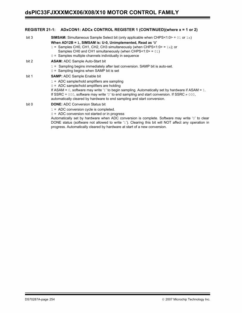
dsPIC33FJXXXMCX06/X08/X10 MOTOR CONTROL FAMILY
bit 3 SIMSAM: Simultaneous Sample Select bit (only applicable when CHPS<1:0> = 01 or 1x)When AD12B = 1, SIMSAM is: U-0, Unimplemented, Read as ‘0’1 = Samples CH0, CH1, CH2, CH3 simultaneously (when CHPS<1:0> = 1x); or
Samples CH0 and CH1 simultaneously (when CHPS<1:0> = 01)0 = Samples multiple channels individually in sequence
bit 2 ASAM: ADC Sample Auto-Start bit1 = Sampling begins immediately after last conversion. SAMP bit is auto-set.0 = Sampling begins when SAMP bit is set
bit 1 SAMP: ADC Sample Enable bit1 = ADC sample/hold amplifiers are sampling0 = ADC sample/hold amplifiers are holdingIf ASAM = 0, software may write ‘1’ to begin sampling. Automatically set by hardware if ASAM = 1.If SSRC = 000, software may write ‘0’ to end sampling and start conversion. If SSRC ≠ 000, automatically cleared by hardware to end sampling and start conversion.
bit 0 DONE: ADC Conversion Status bit 1 = ADC conversion cycle is completed.0 = ADC conversion not started or in progressAutomatically set by hardware when ADC conversion is complete. Software may write ‘0’ to clearDONE status (software not allowed to write ‘1’). Clearing this bit will NOT affect any operation inprogress. Automatically cleared by hardware at start of a new conversion.
REGISTER 21-1: ADxCON1: ADCx CONTROL REGISTER 1 (CONTINUED)(where x = 1 or 2)
DS70287A-page 254 © 2007 Microchip Technology Inc.
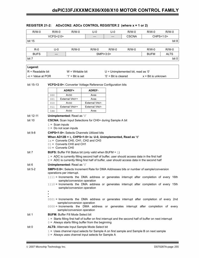
dsPIC33FJXXXMCX06/X08/X10 MOTOR CONTROL FAMILY
REGISTER 21-2: ADxCON2: ADCx CONTROL REGISTER 2 (where x = 1 or 2)
R/W-0 R/W-0 R/W-0 U-0 U-0 R/W-0 R/W-0 R/W-0VCFG<2:0> — — CSCNA CHPS<1:0>
bit 15 bit 8
R-0 U-0 R/W-0 R/W-0 R/W-0 R/W-0 R/W-0 R/W-0BUFS — SMPI<3:0> BUFM ALTS
bit 7 bit 0
Legend:R = Readable bit W = Writable bit U = Unimplemented bit, read as ‘0’-n = Value at POR ‘1’ = Bit is set ‘0’ = Bit is cleared x = Bit is unknown
bit 15-13 VCFG<2:0>: Converter Voltage Reference Configuration bits
bit 12-11 Unimplemented: Read as ‘0’bit 10 CSCNA: Scan Input Selections for CH0+ during Sample A bit
1 = Scan inputs0 = Do not scan inputs
bit 9-8 CHPS<1:0>: Selects Channels Utilized bitsWhen AD12B = 1, CHPS<1:0> is: U-0, Unimplemented, Read as ‘0’ 1x = Converts CH0, CH1, CH2 and CH301 = Converts CH0 and CH100 = Converts CH0
bit 7 BUFS: Buffer Fill Status bit (only valid when BUFM = 1)1 = ADC is currently filling second half of buffer, user should access data in the first half0 = ADC is currently filling first half of buffer, user should access data in the second half
bit 6 Unimplemented: Read as ‘0’bit 5-2 SMPI<3:0>: Selects Increment Rate for DMA Addresses bits or number of sample/conversion
operations per interrupt.1111 = Increments the DMA address or generates interrupt after completion of every 16th
sample/conversion operation1110 = Increments the DMA address or generates interrupt after completion of every 15th
sample/conversion operation• • •0001 = Increments the DMA address or generates interrupt after completion of every 2nd
sample/conversion operation0000 = Increments the DMA address or generates interrupt after completion of every
sample/conversion operationbit 1 BUFM: Buffer Fill Mode Select bit
1 = Starts filling first half of buffer on first interrupt and the second half of buffer on next interrupt0 = Always starts filling buffer from the beginning
bit 0 ALTS: Alternate Input Sample Mode Select bit1 = Uses channel input selects for Sample A on first sample and Sample B on next sample0 = Always uses channel input selects for Sample A
ADREF+ ADREF-
000 AVDD Avss001 External VREF+ Avss010 AVDD External VREF-011 External VREF+ External VREF-1xx AVDD Avss
© 2007 Microchip Technology Inc. DS70287A-page 255
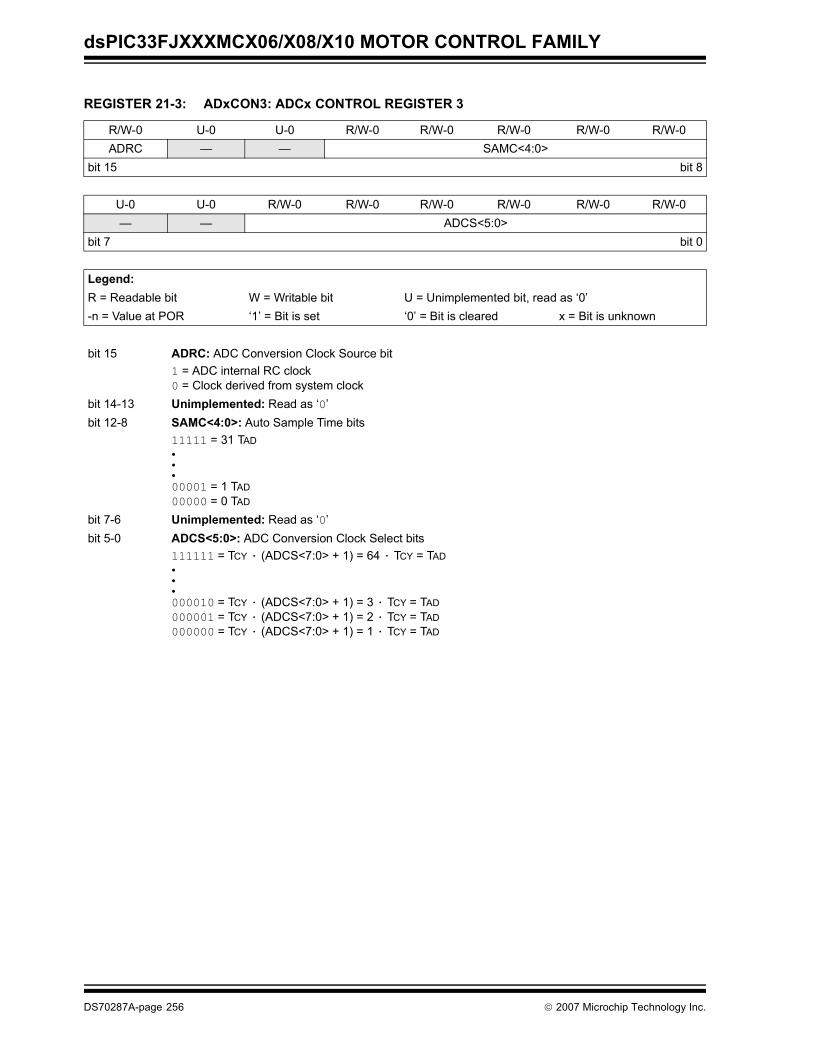
dsPIC33FJXXXMCX06/X08/X10 MOTOR CONTROL FAMILY
REGISTER 21-3: ADxCON3: ADCx CONTROL REGISTER 3
R/W-0 U-0 U-0 R/W-0 R/W-0 R/W-0 R/W-0 R/W-0ADRC — — SAMC<4:0>
bit 15 bit 8
U-0 U-0 R/W-0 R/W-0 R/W-0 R/W-0 R/W-0 R/W-0— — ADCS<5:0>
bit 7 bit 0
Legend:R = Readable bit W = Writable bit U = Unimplemented bit, read as ‘0’-n = Value at POR ‘1’ = Bit is set ‘0’ = Bit is cleared x = Bit is unknown
bit 15 ADRC: ADC Conversion Clock Source bit1 = ADC internal RC clock0 = Clock derived from system clock
bit 14-13 Unimplemented: Read as ‘0’bit 12-8 SAMC<4:0>: Auto Sample Time bits
11111 = 31 TAD• • •00001 = 1 TAD00000 = 0 TAD
bit 7-6 Unimplemented: Read as ‘0’bit 5-0 ADCS<5:0>: ADC Conversion Clock Select bits
111111 = TCY · (ADCS<7:0> + 1) = 64 · TCY = TAD• • •000010 = TCY · (ADCS<7:0> + 1) = 3 · TCY = TAD 000001 = TCY · (ADCS<7:0> + 1) = 2 · TCY = TAD000000 = TCY · (ADCS<7:0> + 1) = 1 · TCY = TAD
DS70287A-page 256 © 2007 Microchip Technology Inc.
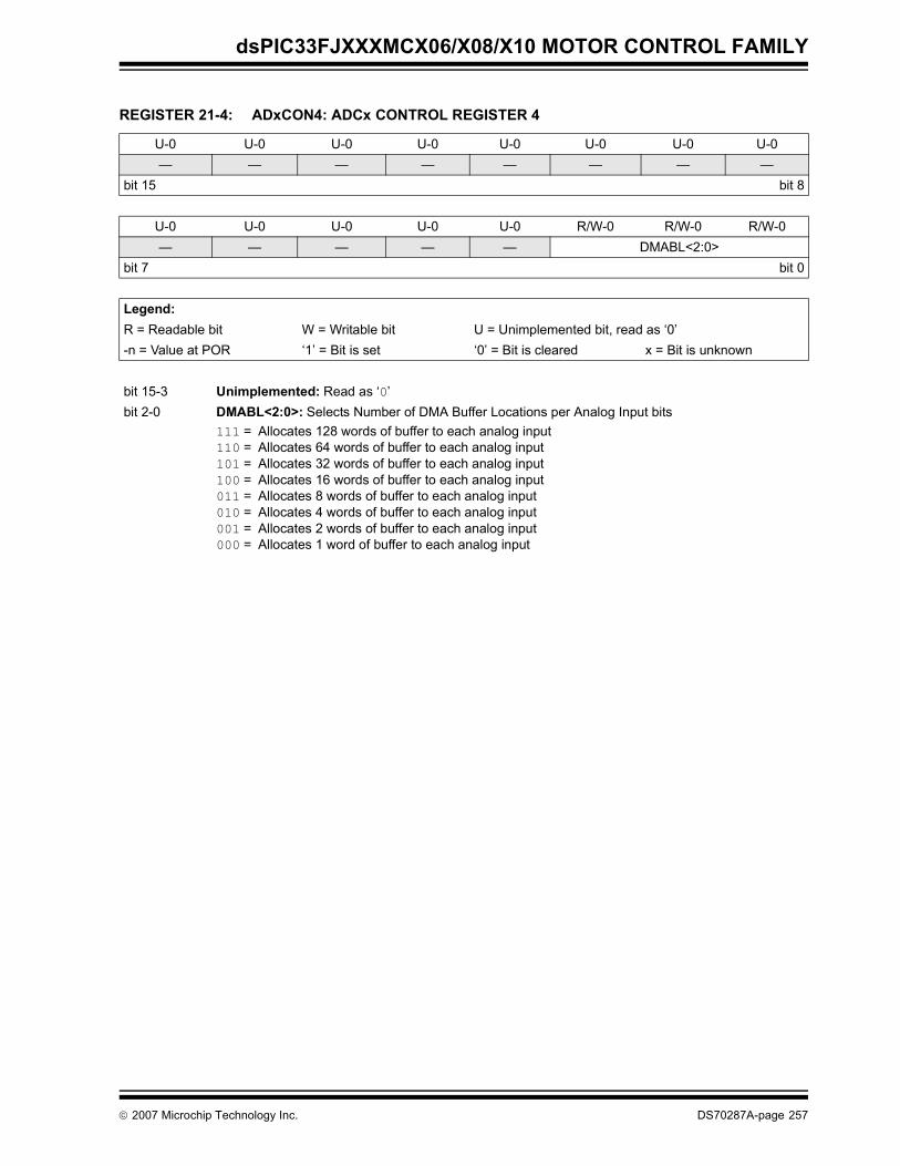
dsPIC33FJXXXMCX06/X08/X10 MOTOR CONTROL FAMILY
REGISTER 21-4: ADxCON4: ADCx CONTROL REGISTER 4
U-0 U-0 U-0 U-0 U-0 U-0 U-0 U-0— — — — — — — —
bit 15 bit 8
U-0 U-0 U-0 U-0 U-0 R/W-0 R/W-0 R/W-0— — — — — DMABL<2:0>
bit 7 bit 0
Legend:R = Readable bit W = Writable bit U = Unimplemented bit, read as ‘0’-n = Value at POR ‘1’ = Bit is set ‘0’ = Bit is cleared x = Bit is unknown
bit 15-3 Unimplemented: Read as ‘0’bit 2-0 DMABL<2:0>: Selects Number of DMA Buffer Locations per Analog Input bits
111 = Allocates 128 words of buffer to each analog input110 = Allocates 64 words of buffer to each analog input101 = Allocates 32 words of buffer to each analog input100 = Allocates 16 words of buffer to each analog input011 = Allocates 8 words of buffer to each analog input010 = Allocates 4 words of buffer to each analog input001 = Allocates 2 words of buffer to each analog input000 = Allocates 1 word of buffer to each analog input
© 2007 Microchip Technology Inc. DS70287A-page 257
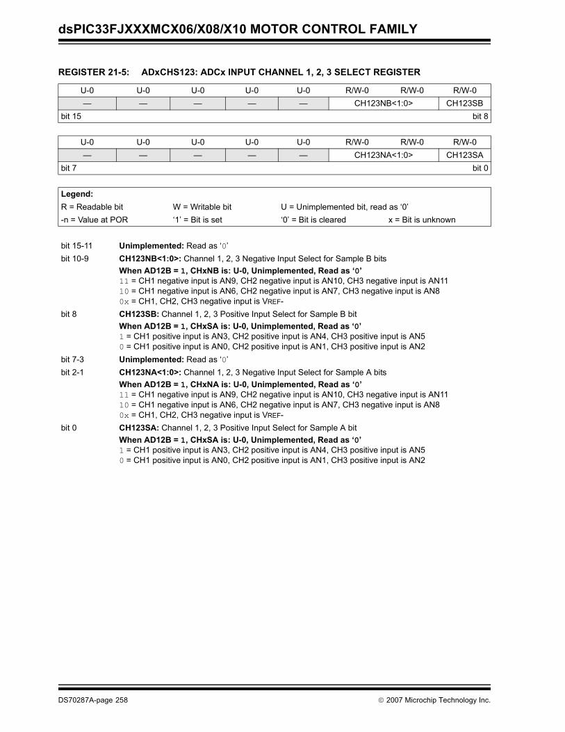
dsPIC33FJXXXMCX06/X08/X10 MOTOR CONTROL FAMILY
REGISTER 21-5: ADxCHS123: ADCx INPUT CHANNEL 1, 2, 3 SELECT REGISTER
U-0 U-0 U-0 U-0 U-0 R/W-0 R/W-0 R/W-0— — — — — CH123NB<1:0> CH123SB
bit 15 bit 8
U-0 U-0 U-0 U-0 U-0 R/W-0 R/W-0 R/W-0— — — — — CH123NA<1:0> CH123SA
bit 7 bit 0
Legend:R = Readable bit W = Writable bit U = Unimplemented bit, read as ‘0’-n = Value at POR ‘1’ = Bit is set ‘0’ = Bit is cleared x = Bit is unknown
bit 15-11 Unimplemented: Read as ‘0’bit 10-9 CH123NB<1:0>: Channel 1, 2, 3 Negative Input Select for Sample B bits
When AD12B = 1, CHxNB is: U-0, Unimplemented, Read as ‘0’11 = CH1 negative input is AN9, CH2 negative input is AN10, CH3 negative input is AN1110 = CH1 negative input is AN6, CH2 negative input is AN7, CH3 negative input is AN80x = CH1, CH2, CH3 negative input is VREF-
bit 8 CH123SB: Channel 1, 2, 3 Positive Input Select for Sample B bitWhen AD12B = 1, CHxSA is: U-0, Unimplemented, Read as ‘0’1 = CH1 positive input is AN3, CH2 positive input is AN4, CH3 positive input is AN50 = CH1 positive input is AN0, CH2 positive input is AN1, CH3 positive input is AN2
bit 7-3 Unimplemented: Read as ‘0’bit 2-1 CH123NA<1:0>: Channel 1, 2, 3 Negative Input Select for Sample A bits
When AD12B = 1, CHxNA is: U-0, Unimplemented, Read as ‘0’11 = CH1 negative input is AN9, CH2 negative input is AN10, CH3 negative input is AN1110 = CH1 negative input is AN6, CH2 negative input is AN7, CH3 negative input is AN80x = CH1, CH2, CH3 negative input is VREF-
bit 0 CH123SA: Channel 1, 2, 3 Positive Input Select for Sample A bitWhen AD12B = 1, CHxSA is: U-0, Unimplemented, Read as ‘0’1 = CH1 positive input is AN3, CH2 positive input is AN4, CH3 positive input is AN50 = CH1 positive input is AN0, CH2 positive input is AN1, CH3 positive input is AN2
DS70287A-page 258 © 2007 Microchip Technology Inc.
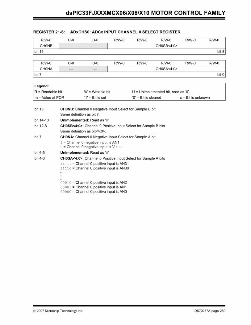
dsPIC33FJXXXMCX06/X08/X10 MOTOR CONTROL FAMILY
REGISTER 21-6: ADxCHS0: ADCx INPUT CHANNEL 0 SELECT REGISTER
R/W-0 U-0 U-0 R/W-0 R/W-0 R/W-0 R/W-0 R/W-0CH0NB — — CH0SB<4:0>
bit 15 bit 8
R/W-0 U-0 U-0 R/W-0 R/W-0 R/W-0 R/W-0 R/W-0CH0NA — — CH0SA<4:0>
bit 7 bit 0
Legend:R = Readable bit W = Writable bit U = Unimplemented bit, read as ‘0’-n = Value at POR ‘1’ = Bit is set ‘0’ = Bit is cleared x = Bit is unknown
bit 15 CH0NB: Channel 0 Negative Input Select for Sample B bitSame definition as bit 7.
bit 14-13 Unimplemented: Read as ‘0’bit 12-8 CH0SB<4:0>: Channel 0 Positive Input Select for Sample B bits
Same definition as bit<4:0>.bit 7 CH0NA: Channel 0 Negative Input Select for Sample A bit
1 = Channel 0 negative input is AN10 = Channel 0 negative input is VREF-
bit 6-5 Unimplemented: Read as ‘0’bit 4-0 CH0SA<4:0>: Channel 0 Positive Input Select for Sample A bits
11111 = Channel 0 positive input is AN3111110 = Channel 0 positive input is AN30• • •00010 = Channel 0 positive input is AN200001 = Channel 0 positive input is AN100000 = Channel 0 positive input is AN0
© 2007 Microchip Technology Inc. DS70287A-page 259
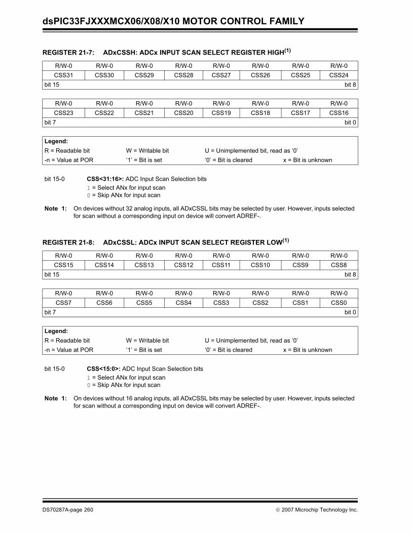
dsPIC33FJXXXMCX06/X08/X10 MOTOR CONTROL FAMILY
REGISTER 21-7: ADxCSSH: ADCx INPUT SCAN SELECT REGISTER HIGH(1)
R/W-0 R/W-0 R/W-0 R/W-0 R/W-0 R/W-0 R/W-0 R/W-0CSS31 CSS30 CSS29 CSS28 CSS27 CSS26 CSS25 CSS24
bit 15 bit 8
R/W-0 R/W-0 R/W-0 R/W-0 R/W-0 R/W-0 R/W-0 R/W-0CSS23 CSS22 CSS21 CSS20 CSS19 CSS18 CSS17 CSS16
bit 7 bit 0
Legend:R = Readable bit W = Writable bit U = Unimplemented bit, read as ‘0’-n = Value at POR ‘1’ = Bit is set ‘0’ = Bit is cleared x = Bit is unknown
bit 15-0 CSS<31:16>: ADC Input Scan Selection bits1 = Select ANx for input scan0 = Skip ANx for input scan
Note 1: On devices without 32 analog inputs, all ADxCSSL bits may be selected by user. However, inputs selected for scan without a corresponding input on device will convert ADREF-.
REGISTER 21-8: ADxCSSL: ADCx INPUT SCAN SELECT REGISTER LOW(1)
R/W-0 R/W-0 R/W-0 R/W-0 R/W-0 R/W-0 R/W-0 R/W-0CSS15 CSS14 CSS13 CSS12 CSS11 CSS10 CSS9 CSS8
bit 15 bit 8
R/W-0 R/W-0 R/W-0 R/W-0 R/W-0 R/W-0 R/W-0 R/W-0CSS7 CSS6 CSS5 CSS4 CSS3 CSS2 CSS1 CSS0
bit 7 bit 0
Legend:R = Readable bit W = Writable bit U = Unimplemented bit, read as ‘0’-n = Value at POR ‘1’ = Bit is set ‘0’ = Bit is cleared x = Bit is unknown
bit 15-0 CSS<15:0>: ADC Input Scan Selection bits1 = Select ANx for input scan0 = Skip ANx for input scan
Note 1: On devices without 16 analog inputs, all ADxCSSL bits may be selected by user. However, inputs selected for scan without a corresponding input on device will convert ADREF-.
DS70287A-page 260 © 2007 Microchip Technology Inc.
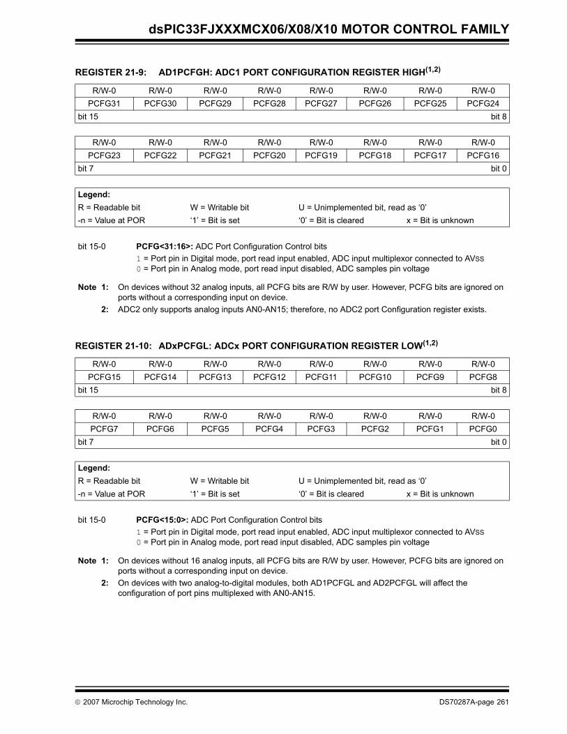
dsPIC33FJXXXMCX06/X08/X10 MOTOR CONTROL FAMILY
REGISTER 21-9: AD1PCFGH: ADC1 PORT CONFIGURATION REGISTER HIGH(1,2)
R/W-0 R/W-0 R/W-0 R/W-0 R/W-0 R/W-0 R/W-0 R/W-0PCFG31 PCFG30 PCFG29 PCFG28 PCFG27 PCFG26 PCFG25 PCFG24
bit 15 bit 8
R/W-0 R/W-0 R/W-0 R/W-0 R/W-0 R/W-0 R/W-0 R/W-0PCFG23 PCFG22 PCFG21 PCFG20 PCFG19 PCFG18 PCFG17 PCFG16
bit 7 bit 0
Legend:R = Readable bit W = Writable bit U = Unimplemented bit, read as ‘0’-n = Value at POR ‘1’ = Bit is set ‘0’ = Bit is cleared x = Bit is unknown
bit 15-0 PCFG<31:16>: ADC Port Configuration Control bits1 = Port pin in Digital mode, port read input enabled, ADC input multiplexor connected to AVSS0 = Port pin in Analog mode, port read input disabled, ADC samples pin voltage
Note 1: On devices without 32 analog inputs, all PCFG bits are R/W by user. However, PCFG bits are ignored on ports without a corresponding input on device.
2: ADC2 only supports analog inputs AN0-AN15; therefore, no ADC2 port Configuration register exists.
REGISTER 21-10: ADxPCFGL: ADCx PORT CONFIGURATION REGISTER LOW(1,2)
R/W-0 R/W-0 R/W-0 R/W-0 R/W-0 R/W-0 R/W-0 R/W-0PCFG15 PCFG14 PCFG13 PCFG12 PCFG11 PCFG10 PCFG9 PCFG8
bit 15 bit 8
R/W-0 R/W-0 R/W-0 R/W-0 R/W-0 R/W-0 R/W-0 R/W-0PCFG7 PCFG6 PCFG5 PCFG4 PCFG3 PCFG2 PCFG1 PCFG0
bit 7 bit 0
Legend:R = Readable bit W = Writable bit U = Unimplemented bit, read as ‘0’-n = Value at POR ‘1’ = Bit is set ‘0’ = Bit is cleared x = Bit is unknown
bit 15-0 PCFG<15:0>: ADC Port Configuration Control bits1 = Port pin in Digital mode, port read input enabled, ADC input multiplexor connected to AVSS0 = Port pin in Analog mode, port read input disabled, ADC samples pin voltage
Note 1: On devices without 16 analog inputs, all PCFG bits are R/W by user. However, PCFG bits are ignored on ports without a corresponding input on device.
2: On devices with two analog-to-digital modules, both AD1PCFGL and AD2PCFGL will affect the configuration of port pins multiplexed with AN0-AN15.
© 2007 Microchip Technology Inc. DS70287A-page 261
dsPIC33FJXXXMCX06/X08/X10 MOTOR CONTROL FAMILY
NOTES:
DS70287A-page 262 © 2007 Microchip Technology Inc.
dsPIC33FJXXXMCX06/X08/X10 MOTOR CONTROL FAMILY
22.0 SPECIAL FEATURES
dsPIC33FJXXXMCX06/X08/X10 Motor Control Familydevices include several features intended to maximizeapplication flexibility and reliability, and minimize costthrough elimination of external components. These are:• Flexible Configuration• Watchdog Timer (WDT)• Code Protection and CodeGuard™ Security• JTAG Boundary Scan Interface• In-Circuit Serial Programming™ (ICSP™)• In-Circuit Emulation
22.1 Configuration BitsThe Configuration bits can be programmed (read as‘0’), or left unprogrammed (read as ‘1’), to select vari-ous device configurations. These bits are mappedstarting at program memory location 0xF80000.
The device Configuration register map is shown inTable 22-1.
The individual Configuration bit descriptions for theFBS, FSS, FGS, FOSCSEL, FOSC, FWDT, FPOR andFICD Configuration registers are shown in Table 22-2.
Note that address 0xF80000 is beyond the user programmemory space. In fact, it belongs to the configurationmemory space (0x800000-0xFFFFFF) which can only beaccessed using table reads and table writes.The upper byte of all device Configuration registersshould always be ‘1111 1111’. This makes themappear to be NOP instructions in the remote event thattheir locations are ever executed by accident. SinceConfiguration bits are not implemented in thecorresponding locations, writing ‘1’s to these locationshas no effect on device operation.
To prevent inadvertent configuration changes duringcode execution, all programmable Configuration bitsare write-once. After a bit is initially programmed duringa power cycle, it cannot be written to again. Changinga device configuration requires that power to the devicebe cycled.
Note: This data sheet summarizes the featuresof this groupof dsPIC33FJXXXMCX06/X08/X10 MotorControl Family devices. It is not intendedto be a comprehensive reference source.To complement the information in this datasheet, refer to the “dsPIC33F FamilyReference Manual”. Refer to theMicrochip web site (www.microchip.com)for the latest dsPIC33F family referencemanual chapters.
TABLE 22-1: DEVICE CONFIGURATION REGISTER MAPAddress Name Bit 7 Bit 6 Bit 5 Bit 4 Bit 3 Bit 2 Bit 1 Bit 0
0xF80000 FBS RBS<1:0> — — BSS<2:0> BWRP0xF80002 FSS RSS<1:0> — — SSS<2:0> SWRP0xF80004 FGS — — — — — GSS1 GSS0 GWRP0xF80006 FOSCSEL IESO — — — — FNOSC<2:0>0xF80008 FOSC FCKSM<1:0> — — — OSCIOFNC POSCMD<1:0>0xF8000A FWDT FWDTEN WINDIS — WDTPRE WDTPOST<3:0>0xF8000C FPOR PWMPIN HPOL LPOL — — FPWRT<2:0>0xF8000E RESERVED3 Reserved(1)
0xF80010 FUID0 User Unit ID Byte 00xF80012 FUID1 User Unit ID Byte 10xF80014 FUID2 User Unit ID Byte 20xF80016 FUID3 User Unit ID Byte 3Note 1: These reserved bits read as ‘1’ and must be programmed as ‘1’.
2: Unimplemented bits are read as ‘0’.
© 2007 Microchip Technology Inc. DS70287A-page 263
dsPIC33FJXXXMCX06/X08/X10 MOTOR CONTROL FAMILY
TABLE 22-2: DSPIC33F CONFIGURATION BITS DESCRIPTIONBit Field Register Description
BWRP FBS Boot Segment Program Flash Write Protection1 = Boot segment may be written0 = Boot segment is write-protected
BSS<2:0> FBS Boot Segment Program Flash Code Protection SizeX11 = No Boot program Flash segment
Boot space is 1K IW less VS110 = Standard security; boot program Flash segment starts at End of
VS, ends at 0007FEh010 = High security; boot program Flash segment starts at End of VS,
ends at 0007FEh
Boot space is 4K IW less VS101 = Standard security; boot program Flash segment starts at End of
VS, ends at 001FFEh001 = High security; boot program Flash segment starts at End of VS,
ends at 001FFEh
Boot space is 8K IW less VS100 = Standard security; boot program Flash segment starts at End of
VS, ends at 003FFEh000 = High security; boot program Flash segment starts at End of VS,
ends at 003FFEh
RBS<1:0> FBS Boot Segment RAM Code Protection10 = No Boot RAM defined10 = Boot RAM is 128 Bytes01 = Boot RAM is 256 Bytes00 = Boot RAM is 1024 Bytes
SWRP FSS Secure Segment Program Flash Write Protection1 = Secure segment may be written0 = Secure segment is write-protected.
DS70287A-page 264 © 2007 Microchip Technology Inc.
dsPIC33FJXXXMCX06/X08/X10 MOTOR CONTROL FAMILY
SSS<2:0> FSS Secure Segment Program Flash Code Protection Size
(FOR 128K and 256K DEVICES)X11 = No Secure program Flash segment
Secure space is 8K IW less BS110 = Standard security; secure program Flash segment starts at End
of BS, ends at 0x003FFE010 = High security; secure program Flash segment starts at End of
BS, ends at 0x003FFE
Secure space is 16K IW less BS101 = Standard security; secure program Flash segment starts at End
of BS, ends at 0x007FFE001 = High security; secure program Flash segment starts at End of
BS, ends at 0x007FFE
Secure space is 32K IW less BS100 = Standard security; secure program Flash segment starts at End
of BS, ends at 0x00FFFE000 = High security; secure program Flash segment starts at End of
BS, ends at 0x00FFFE
(FOR 64K DEVICES)X11 = No Secure program Flash segment
Secure space is 4K IW less BS110 = Standard security; secure program Flash segment starts at End
of BS, ends at 0x001FFE010 = High security; secure program Flash segment starts at End of
BS, ends at 0x001FFE
Secure space is 8K IW less BS101 = Standard security; secure program Flash segment starts at End
of BS, ends at 0x003FFE001 = High security; secure program Flash segment starts at End of
BS, ends at 0x003FFE
Secure space is 16K IW less BS100 = Standard security; secure program Flash segment starts at End
of BS, ends at 007FFEh000 = High security; secure program Flash segment starts at End of
BS, ends at 0x007FFE
RSS<1:0> FSS Secure Segment RAM Code Protection10 = No Secure RAM defined10 = Secure RAM is 256 Bytes less BS RAM01 = Secure RAM is 2048 Bytes less BS RAM00 = Secure RAM is 4096 Bytes less BS RAM
GSS<1:0> FGS General Segment Code-Protect bit11 = User program memory is not code-protected10 = Standard security; general program Flash segment starts at End
of SS, ends at EOM0x = High security; general program Flash segment starts at End of SS,
ends at EOM
TABLE 22-2: DSPIC33F CONFIGURATION BITS DESCRIPTION (CONTINUED)Bit Field Register Description
© 2007 Microchip Technology Inc. DS70287A-page 265
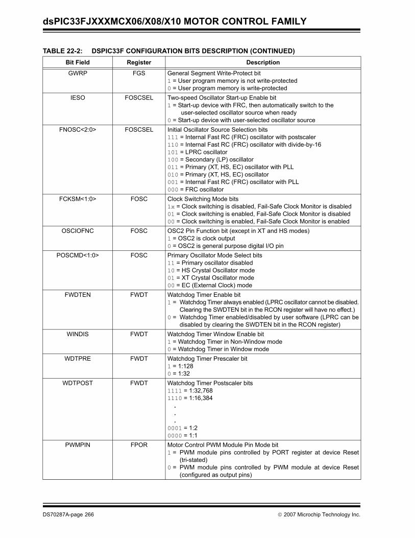
dsPIC33FJXXXMCX06/X08/X10 MOTOR CONTROL FAMILY
GWRP FGS General Segment Write-Protect bit1 = User program memory is not write-protected0 = User program memory is write-protected
IESO FOSCSEL Two-speed Oscillator Start-up Enable bit1 = Start-up device with FRC, then automatically switch to the user-selected oscillator source when ready0 = Start-up device with user-selected oscillator source
FNOSC<2:0> FOSCSEL Initial Oscillator Source Selection bits111 = Internal Fast RC (FRC) oscillator with postscaler110 = Internal Fast RC (FRC) oscillator with divide-by-16101 = LPRC oscillator100 = Secondary (LP) oscillator011 = Primary (XT, HS, EC) oscillator with PLL010 = Primary (XT, HS, EC) oscillator001 = Internal Fast RC (FRC) oscillator with PLL000 = FRC oscillator
FCKSM<1:0> FOSC Clock Switching Mode bits1x = Clock switching is disabled, Fail-Safe Clock Monitor is disabled01 = Clock switching is enabled, Fail-Safe Clock Monitor is disabled00 = Clock switching is enabled, Fail-Safe Clock Monitor is enabled
OSCIOFNC FOSC OSC2 Pin Function bit (except in XT and HS modes)1 = OSC2 is clock output0 = OSC2 is general purpose digital I/O pin
POSCMD<1:0> FOSC Primary Oscillator Mode Select bits11 = Primary oscillator disabled10 = HS Crystal Oscillator mode01 = XT Crystal Oscillator mode00 = EC (External Clock) mode
FWDTEN FWDT Watchdog Timer Enable bit1 = Watchdog Timer always enabled (LPRC oscillator cannot be disabled.
Clearing the SWDTEN bit in the RCON register will have no effect.)0 = Watchdog Timer enabled/disabled by user software (LPRC can be
disabled by clearing the SWDTEN bit in the RCON register)WINDIS FWDT Watchdog Timer Window Enable bit
1 = Watchdog Timer in Non-Window mode0 = Watchdog Timer in Window mode
WDTPRE FWDT Watchdog Timer Prescaler bit1 = 1:1280 = 1:32
WDTPOST FWDT Watchdog Timer Postscaler bits1111 = 1:32,7681110 = 1:16,384 . . .0001 = 1:20000 = 1:1
PWMPIN FPOR Motor Control PWM Module Pin Mode bit1 = PWM module pins controlled by PORT register at device Reset
(tri-stated)0 = PWM module pins controlled by PWM module at device Reset
(configured as output pins)
TABLE 22-2: DSPIC33F CONFIGURATION BITS DESCRIPTION (CONTINUED)Bit Field Register Description
DS70287A-page 266 © 2007 Microchip Technology Inc.
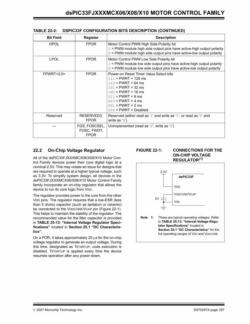
dsPIC33FJXXXMCX06/X08/X10 MOTOR CONTROL FAMILY
22.2 On-Chip Voltage RegulatorAll of the dsPIC33FJXXXMCX06/X08/X10 Motor Con-trol Family devices power their core digital logic at anominal 2.5V. This may create an issue for designs thatare required to operate at a higher typical voltage, suchas 3.3V. To simplify system design, all devices in thedsPIC33FJXXXMCX06/X08/X10 Motor Control Familyfamily incorporate an on-chip regulator that allows thedevice to run its core logic from VDD.
The regulator provides power to the core from the otherVDD pins. The regulator requires that a low-ESR (lessthan 5 ohms) capacitor (such as tantalum or ceramic)be connected to the VDDCORE/VCAP pin (Figure 22-1).This helps to maintain the stability of the regulator. Therecommended value for the filter capacitor is providedin TABLE 25-13: “Internal Voltage Regulator Speci-fications” located in Section 25.1 “DC Characteris-tics”.
On a POR, it takes approximately 20 μs for the on-chipvoltage regulator to generate an output voltage. Duringthis time, designated as TSTARTUP, code execution isdisabled. TSTARTUP is applied every time the deviceresumes operation after any power-down.
FIGURE 22-1: CONNECTIONS FOR THE ON-CHIP VOLTAGE REGULATOR(1)
HPOL FPOR Motor Control PWM High Side Polarity bit1 = PWM module high side output pins have active-high output polarity0 = PWM module high side output pins have active-low output polarity
LPOL FPOR Motor Control PWM Low Side Polarity bit1 = PWM module low side output pins have active-high output polarity0 = PWM module low side output pins have active-low output polarity
FPWRT<2:0> FPOR Power-on Reset Timer Value Select bits111 = PWRT = 128 ms110 = PWRT = 64 ms101 = PWRT = 32 ms100 = PWRT = 16 ms011 = PWRT = 8 ms010 = PWRT = 4 ms001 = PWRT = 2 ms000 = PWRT = Disabled
Reserved RESERVED3, FPOR
Reserved (either read as ‘1’ and write as ‘1’, or read as ‘0’ and write as ‘0’)
— FGS, FOSCSEL, FOSC, FWDT,
FPOR
Unimplemented (read as ‘0’, write as ‘0’)
TABLE 22-2: DSPIC33F CONFIGURATION BITS DESCRIPTION (CONTINUED)Bit Field Register Description
Note 1: These are typical operating voltages. Refer to TABLE 25-13: “Internal Voltage Regu-lator Specifications” located in Section 25.1 “DC Characteristics” for the full operating ranges of VDD and VDDCORE.
VDD
VDDCORE/VCAP
VSS
dsPIC33F
CF
3.3V
© 2007 Microchip Technology Inc. DS70287A-page 267
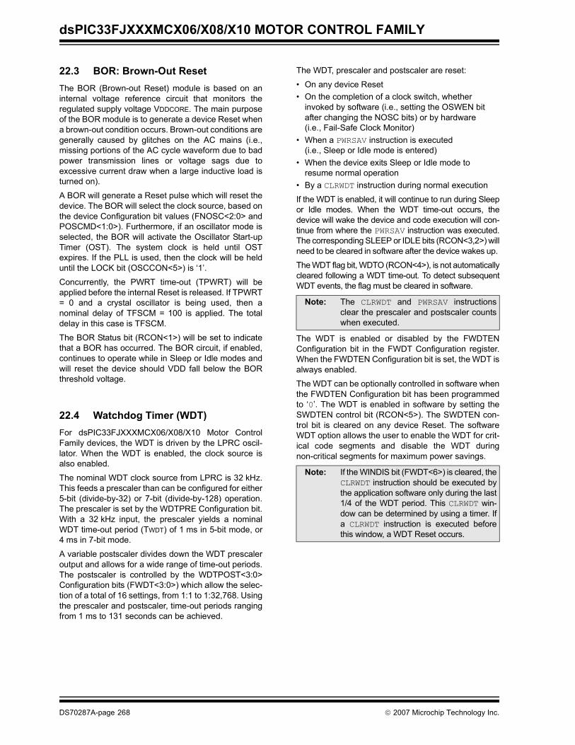
dsPIC33FJXXXMCX06/X08/X10 MOTOR CONTROL FAMILY
22.3 BOR: Brown-Out ResetThe BOR (Brown-out Reset) module is based on aninternal voltage reference circuit that monitors theregulated supply voltage VDDCORE. The main purposeof the BOR module is to generate a device Reset whena brown-out condition occurs. Brown-out conditions aregenerally caused by glitches on the AC mains (i.e.,missing portions of the AC cycle waveform due to badpower transmission lines or voltage sags due toexcessive current draw when a large inductive load isturned on).
A BOR will generate a Reset pulse which will reset thedevice. The BOR will select the clock source, based onthe device Configuration bit values (FNOSC<2:0> andPOSCMD<1:0>). Furthermore, if an oscillator mode isselected, the BOR will activate the Oscillator Start-upTimer (OST). The system clock is held until OSTexpires. If the PLL is used, then the clock will be helduntil the LOCK bit (OSCCON<5>) is ‘1’.
Concurrently, the PWRT time-out (TPWRT) will beapplied before the internal Reset is released. If TPWRT= 0 and a crystal oscillator is being used, then anominal delay of TFSCM = 100 is applied. The totaldelay in this case is TFSCM.
The BOR Status bit (RCON<1>) will be set to indicatethat a BOR has occurred. The BOR circuit, if enabled,continues to operate while in Sleep or Idle modes andwill reset the device should VDD fall below the BORthreshold voltage.
22.4 Watchdog Timer (WDT)For dsPIC33FJXXXMCX06/X08/X10 Motor ControlFamily devices, the WDT is driven by the LPRC oscil-lator. When the WDT is enabled, the clock source isalso enabled.
The nominal WDT clock source from LPRC is 32 kHz.This feeds a prescaler than can be configured for either5-bit (divide-by-32) or 7-bit (divide-by-128) operation.The prescaler is set by the WDTPRE Configuration bit.With a 32 kHz input, the prescaler yields a nominalWDT time-out period (TWDT) of 1 ms in 5-bit mode, or4 ms in 7-bit mode.
A variable postscaler divides down the WDT prescaleroutput and allows for a wide range of time-out periods.The postscaler is controlled by the WDTPOST<3:0>Configuration bits (FWDT<3:0>) which allow the selec-tion of a total of 16 settings, from 1:1 to 1:32,768. Usingthe prescaler and postscaler, time-out periods rangingfrom 1 ms to 131 seconds can be achieved.
The WDT, prescaler and postscaler are reset:
• On any device Reset• On the completion of a clock switch, whether
invoked by software (i.e., setting the OSWEN bit after changing the NOSC bits) or by hardware (i.e., Fail-Safe Clock Monitor)
• When a PWRSAV instruction is executed (i.e., Sleep or Idle mode is entered)
• When the device exits Sleep or Idle mode to resume normal operation
• By a CLRWDT instruction during normal execution
If the WDT is enabled, it will continue to run during Sleepor Idle modes. When the WDT time-out occurs, thedevice will wake the device and code execution will con-tinue from where the PWRSAV instruction was executed.The corresponding SLEEP or IDLE bits (RCON<3,2>) willneed to be cleared in software after the device wakes up.
The WDT flag bit, WDTO (RCON<4>), is not automaticallycleared following a WDT time-out. To detect subsequentWDT events, the flag must be cleared in software.
The WDT is enabled or disabled by the FWDTENConfiguration bit in the FWDT Configuration register.When the FWDTEN Configuration bit is set, the WDT isalways enabled.
The WDT can be optionally controlled in software whenthe FWDTEN Configuration bit has been programmedto ‘0’. The WDT is enabled in software by setting theSWDTEN control bit (RCON<5>). The SWDTEN con-trol bit is cleared on any device Reset. The softwareWDT option allows the user to enable the WDT for crit-ical code segments and disable the WDT duringnon-critical segments for maximum power savings.
Note: The CLRWDT and PWRSAV instructionsclear the prescaler and postscaler countswhen executed.
Note: If the WINDIS bit (FWDT<6>) is cleared, theCLRWDT instruction should be executed bythe application software only during the last1/4 of the WDT period. This CLRWDT win-dow can be determined by using a timer. Ifa CLRWDT instruction is executed beforethis window, a WDT Reset occurs.
DS70287A-page 268 © 2007 Microchip Technology Inc.
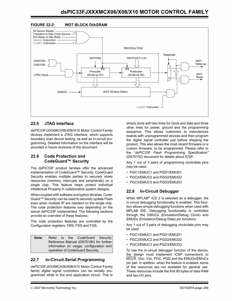
dsPIC33FJXXXMCX06/X08/X10 MOTOR CONTROL FAMILY
FIGURE 22-2: WDT BLOCK DIAGRAM
22.5 JTAG InterfacedsPIC33FJXXXMCX06/X08/X10 Motor Control Familydevices implement a JTAG interface, which supportsboundary scan device testing, as well as in-circuit pro-gramming. Detailed information on the interface will beprovided in future revisions of the document.
22.6 Code Protection and CodeGuard™ Security
The dsPIC33F product families offer the advancedimplementation of CodeGuard™ Security. CodeGuardSecurity enables multiple parties to securely shareresources (memory, interrupts and peripherals) on asingle chip. This feature helps protect individualIntellectual Property in collaborative system designs.
When coupled with software encryption libraries, Code-Guard™ Security can be used to securely update Flasheven when multiple IP are resident on the single chip.The code protection features vary depending on theactual dsPIC33F implemented. The following sectionsprovide an overview of these features.
The code protection features are controlled by theConfiguration registers: FBS, FSS and FGS.
22.7 In-Circuit Serial ProgrammingdsPIC33FJXXXMCX06/X08/X10 Motor Control Familyfamily digital signal controllers can be serially pro-grammed while in the end application circuit. This is
simply done with two lines for clock and data and threeother lines for power, ground and the programmingsequence. This allows customers to manufactureboards with unprogrammed devices and then programthe digital signal controller just before shipping theproduct. This also allows the most recent firmware or acustom firmware, to be programmed. Please refer tothe “dsPIC33F Flash Programming Specification”(DS70152) document for details about ICSP.
Any 1 out of 3 pairs of programming clock/data pinsmay be used:
• PGC1/EMUC1 and PGD1/EMUD1• PGC2/EMUC2 and PGD2/EMUD2 • PGC3/EMUC3 and PGD3/EMUD3
22.8 In-Circuit DebuggerWhen MPLAB® ICD 2 is selected as a debugger, thein-circuit debugging functionality is enabled. This func-tion allows simple debugging functions when used withMPLAB IDE. Debugging functionality is controlledthrough the EMUCx (Emulation/Debug Clock) andEMUDx (Emulation/Debug Data) pin functions.
Any 1 out of 3 pairs of debugging clock/data pins maybe used:
• PGC1/EMUC1 and PGD1/EMUD1• PGC2/EMUC2 and PGD2/EMUD2 • PGC3/EMUC3 and PGD3/EMUD3
To use the in-circuit debugger function of the device,the design must implement ICSP connections toMCLR, VDD, VSS, PGC, PGD and the EMUDx/EMUCxpin pair. In addition, when the feature is enabled, someof the resources are not available for general use.These resources include the first 80 bytes of data RAMand two I/O pins.
All Device ResetsTransition to New Clock SourceExit Sleep or Idle ModePWRSAV InstructionCLRWDT Instruction
0
1
WDTPRE WDTPOST<3:0>
Watchdog Timer
Prescaler(divide by N1)
Postscaler(divide by N2)
Sleep/Idle
WDT
WDT Window SelectWINDIS
WDT
CLRWDT Instruction
SWDTENFWDTEN
LPRC Clock
RS RS
Wake-up
Reset
Note: Refer to the CodeGuard SecurityReference Manual (DS70180) for furtherinformation on usage, configuration andoperation of CodeGuard Security.
© 2007 Microchip Technology Inc. DS70287A-page 269

dsPIC33FJXXXMCX06/X08/X10 MOTOR CONTROL FAMILY
NOTES:
DS70287A-page 270 © 2007 Microchip Technology Inc.
dsPIC33FJXXXMCX06/X08/X10 Motor Control Family
23.0 INSTRUCTION SET SUMMARY
The dsPIC33F instruction set is identical to that of thedsPIC30F.
Most instructions are a single program memory word(24 bits). Only three instructions require two programmemory locations.
Each single-word instruction is a 24-bit word, dividedinto an 8-bit opcode, which specifies the instructiontype and one or more operands, which further specifythe operation of the instruction.
The instruction set is highly orthogonal and is groupedinto five basic categories:
• Word or byte-oriented operations• Bit-oriented operations• Literal operations• DSP operations• Control operations
Table 23-1 shows the general symbols used indescribing the instructions.
The dsPIC33F instruction set summary in Table 23-2lists all the instructions, along with the status flagsaffected by each instruction.
Most word or byte-oriented W register instructions(including barrel shift instructions) have threeoperands:
• The first source operand which is typically a register ‘Wb’ without any address modifier
• The second source operand which is typically a register ‘Ws’ with or without an address modifier
• The destination of the result which is typically a register ‘Wd’ with or without an address modifier
However, word or byte-oriented file register instructionshave two operands:
• The file register specified by the value ‘f’• The destination, which could either be the file
register ‘f’ or the W0 register, which is denoted as ‘WREG’
Most bit-oriented instructions (including simple rotate/shift instructions) have two operands:
• The W register (with or without an address modifier) or file register (specified by the value of ‘Ws’ or ‘f’)
• The bit in the W register or file register (specified by a literal value or indirectly by the contents of register ‘Wb’)
The literal instructions that involve data movement mayuse some of the following operands:
• A literal value to be loaded into a W register or file register (specified by the value of ‘k’)
• The W register or file register where the literal value is to be loaded (specified by ‘Wb’ or ‘f’)
However, literal instructions that involve arithmetic orlogical operations use some of the following operands:
• The first source operand which is a register ‘Wb’ without any address modifier
• The second source operand which is a literal value
• The destination of the result (only if not the same as the first source operand) which is typically a register ‘Wd’ with or without an address modifier
The MAC class of DSP instructions may use some of thefollowing operands:
• The accumulator (A or B) to be used (required operand)
• The W registers to be used as the two operands• The X and Y address space prefetch operations• The X and Y address space prefetch destinations• The accumulator write back destination
The other DSP instructions do not involve anymultiplication and may include:
• The accumulator to be used (required)• The source or destination operand (designated as
Wso or Wdo, respectively) with or without an address modifier
• The amount of shift specified by a W register ‘Wn’ or a literal value
The control instructions may use some of the followingoperands:
• A program memory address • The mode of the table read and table write
instructions
Note: This data sheet summarizes the featuresof this group of dsPIC33FJXXXMCX06/X08/X10 Motor Control Family devices. Itis not intended to be a comprehensivereference source. To complement theinformation in this data sheet, refer to the“dsPIC33F Family Reference Manual”.Refer to the Microchip web site(www.microchip.com) for the latestdsPIC33F family reference manualchapters.
© 2007 Microchip Technology Inc. DS70287A-page 271
dsPIC33FJXXXMCX06/X08/X10 Motor Control Family
All instructions are a single word, except for certaindouble-word instructions, which were made double-word instructions so that all the required information isavailable in these 48 bits. In the second word, the8 MSbs are ‘0’s. If this second word is executed as aninstruction (by itself), it will execute as a NOP.
Most single-word instructions are executed in a singleinstruction cycle, unless a conditional test is true, or theprogram counter is changed as a result of the instruc-tion. In these cases, the execution takes two instructioncycles with the additional instruction cycle(s) executedas a NOP. Notable exceptions are the BRA (uncondi-tional/computed branch), indirect CALL/GOTO, all table
reads and writes and RETURN/RETFIE instructions,which are single-word instructions but take two or threecycles. Certain instructions that involve skipping over thesubsequent instruction require either two or three cyclesif the skip is performed, depending on whether theinstruction being skipped is a single-word or two-wordinstruction. Moreover, double-word moves require twocycles. The double-word instructions execute in twoinstruction cycles.
Note: For more details on the instruction set,refer to the “dsPIC30F/33F Programmer’sReference Manual” (DS70157).
TABLE 23-1: SYMBOLS USED IN OPCODE DESCRIPTIONSField Description
#text Means literal defined by “text”(text) Means “content of text”[text] Means “the location addressed by text”{ } Optional field or operation<n:m> Register bit field.b Byte mode selection.d Double-Word mode selection.S Shadow register select.w Word mode selection (default)Acc One of two accumulators {A, B}AWB Accumulator write back destination address register ∈ {W13, [W13]+ = 2}bit4 4-bit bit selection field (used in word addressed instructions) ∈ {0...15}C, DC, N, OV, Z MCU Status bits: Carry, Digit Carry, Negative, Overflow, Sticky ZeroExpr Absolute address, label or expression (resolved by the linker)f File register address ∈ {0x0000...0x1FFF}lit1 1-bit unsigned literal ∈ {0,1}lit4 4-bit unsigned literal ∈ {0...15}lit5 5-bit unsigned literal ∈ {0...31}lit8 8-bit unsigned literal ∈ {0...255}lit10 10-bit unsigned literal ∈ {0...255} for Byte mode, {0:1023} for Word modelit14 14-bit unsigned literal ∈ {0...16384}lit16 16-bit unsigned literal ∈ {0...65535}lit23 23-bit unsigned literal ∈ {0...8388608}; LSb must be ‘0’None Field does not require an entry, may be blankOA, OB, SA, SB DSP Status bits: AccA Overflow, AccB Overflow, AccA Saturate, AccB SaturatePC Program CounterSlit10 10-bit signed literal ∈ {-512...511}Slit16 16-bit signed literal ∈ {-32768...32767}Slit6 6-bit signed literal ∈ {-16...16}Wb Base W register ∈ {W0..W15}Wd Destination W register ∈ { Wd, [Wd], [Wd++], [Wd--], [++Wd], [--Wd] }Wdo Destination W register ∈
{ Wnd, [Wnd], [Wnd++], [Wnd--], [++Wnd], [--Wnd], [Wnd+Wb] } Wm,Wn Dividend, Divisor working register pair (direct addressing)
DS70287A-page 272 © 2007 Microchip Technology Inc.
dsPIC33FJXXXMCX06/X08/X10 Motor Control Family
Wm*Wm Multiplicand and Multiplier working register pair for Square instructions ∈ {W4 * W4,W5 * W5,W6 * W6,W7 * W7}
Wm*Wn Multiplicand and Multiplier working register pair for DSP instructions ∈{W4 * W5,W4 * W6,W4 * W7,W5 * W6,W5 * W7,W6 * W7}
Wn One of 16 working registers ∈ {W0..W15}Wnd One of 16 destination working registers ∈ {W0..W15}Wns One of 16 source working registers ∈ {W0..W15}WREG W0 (working register used in file register instructions)Ws Source W register ∈ { Ws, [Ws], [Ws++], [Ws--], [++Ws], [--Ws] }Wso Source W register ∈
{ Wns, [Wns], [Wns++], [Wns--], [++Wns], [--Wns], [Wns+Wb] } Wx X data space prefetch address register for DSP instructions
∈ {[W8]+ = 6, [W8]+ = 4, [W8]+ = 2, [W8], [W8]- = 6, [W8]- = 4, [W8]- = 2, [W9]+ = 6, [W9]+ = 4, [W9]+ = 2, [W9], [W9]- = 6, [W9]- = 4, [W9]- = 2, [W9 + W12], none}
Wxd X data space prefetch destination register for DSP instructions ∈ {W4..W7}Wy Y data space prefetch address register for DSP instructions
∈ {[W10]+ = 6, [W10]+ = 4, [W10]+ = 2, [W10], [W10]- = 6, [W10]- = 4, [W10]- = 2, [W11]+ = 6, [W11]+ = 4, [W11]+ = 2, [W11], [W11]- = 6, [W11]- = 4, [W11]- = 2, [W11 + W12], none}
Wyd Y data space prefetch destination register for DSP instructions ∈ {W4..W7}
TABLE 23-1: SYMBOLS USED IN OPCODE DESCRIPTIONS (CONTINUED)Field Description
© 2007 Microchip Technology Inc. DS70287A-page 273
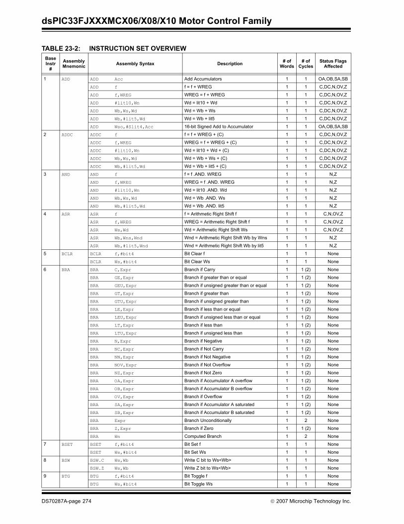
dsPIC33FJXXXMCX06/X08/X10 Motor Control Family
TABLE 23-2: INSTRUCTION SET OVERVIEW BaseInstr
#AssemblyMnemonic Assembly Syntax Description # of
Words# of
CyclesStatus Flags
Affected
1 ADD ADD Acc Add Accumulators 1 1 OA,OB,SA,SB
ADD f f = f + WREG 1 1 C,DC,N,OV,Z
ADD f,WREG WREG = f + WREG 1 1 C,DC,N,OV,Z
ADD #lit10,Wn Wd = lit10 + Wd 1 1 C,DC,N,OV,Z
ADD Wb,Ws,Wd Wd = Wb + Ws 1 1 C,DC,N,OV,Z
ADD Wb,#lit5,Wd Wd = Wb + lit5 1 1 C,DC,N,OV,Z
ADD Wso,#Slit4,Acc 16-bit Signed Add to Accumulator 1 1 OA,OB,SA,SB
2 ADDC ADDC f f = f + WREG + (C) 1 1 C,DC,N,OV,Z
ADDC f,WREG WREG = f + WREG + (C) 1 1 C,DC,N,OV,Z
ADDC #lit10,Wn Wd = lit10 + Wd + (C) 1 1 C,DC,N,OV,Z
ADDC Wb,Ws,Wd Wd = Wb + Ws + (C) 1 1 C,DC,N,OV,Z
ADDC Wb,#lit5,Wd Wd = Wb + lit5 + (C) 1 1 C,DC,N,OV,Z
3 AND AND f f = f .AND. WREG 1 1 N,Z
AND f,WREG WREG = f .AND. WREG 1 1 N,Z
AND #lit10,Wn Wd = lit10 .AND. Wd 1 1 N,Z
AND Wb,Ws,Wd Wd = Wb .AND. Ws 1 1 N,Z
AND Wb,#lit5,Wd Wd = Wb .AND. lit5 1 1 N,Z
4 ASR ASR f f = Arithmetic Right Shift f 1 1 C,N,OV,Z
ASR f,WREG WREG = Arithmetic Right Shift f 1 1 C,N,OV,Z
ASR Ws,Wd Wd = Arithmetic Right Shift Ws 1 1 C,N,OV,Z
ASR Wb,Wns,Wnd Wnd = Arithmetic Right Shift Wb by Wns 1 1 N,Z
ASR Wb,#lit5,Wnd Wnd = Arithmetic Right Shift Wb by lit5 1 1 N,Z
5 BCLR BCLR f,#bit4 Bit Clear f 1 1 None
BCLR Ws,#bit4 Bit Clear Ws 1 1 None
6 BRA BRA C,Expr Branch if Carry 1 1 (2) None
BRA GE,Expr Branch if greater than or equal 1 1 (2) None
BRA GEU,Expr Branch if unsigned greater than or equal 1 1 (2) None
BRA GT,Expr Branch if greater than 1 1 (2) None
BRA GTU,Expr Branch if unsigned greater than 1 1 (2) None
BRA LE,Expr Branch if less than or equal 1 1 (2) None
BRA LEU,Expr Branch if unsigned less than or equal 1 1 (2) None
BRA LT,Expr Branch if less than 1 1 (2) None
BRA LTU,Expr Branch if unsigned less than 1 1 (2) None
BRA N,Expr Branch if Negative 1 1 (2) None
BRA NC,Expr Branch if Not Carry 1 1 (2) None
BRA NN,Expr Branch if Not Negative 1 1 (2) None
BRA NOV,Expr Branch if Not Overflow 1 1 (2) None
BRA NZ,Expr Branch if Not Zero 1 1 (2) None
BRA OA,Expr Branch if Accumulator A overflow 1 1 (2) None
BRA OB,Expr Branch if Accumulator B overflow 1 1 (2) None
BRA OV,Expr Branch if Overflow 1 1 (2) None
BRA SA,Expr Branch if Accumulator A saturated 1 1 (2) None
BRA SB,Expr Branch if Accumulator B saturated 1 1 (2) None
BRA Expr Branch Unconditionally 1 2 None
BRA Z,Expr Branch if Zero 1 1 (2) None
BRA Wn Computed Branch 1 2 None
7 BSET BSET f,#bit4 Bit Set f 1 1 None
BSET Ws,#bit4 Bit Set Ws 1 1 None
8 BSW BSW.C Ws,Wb Write C bit to Ws<Wb> 1 1 None
BSW.Z Ws,Wb Write Z bit to Ws<Wb> 1 1 None
9 BTG BTG f,#bit4 Bit Toggle f 1 1 None
BTG Ws,#bit4 Bit Toggle Ws 1 1 None
DS70287A-page 274 © 2007 Microchip Technology Inc.
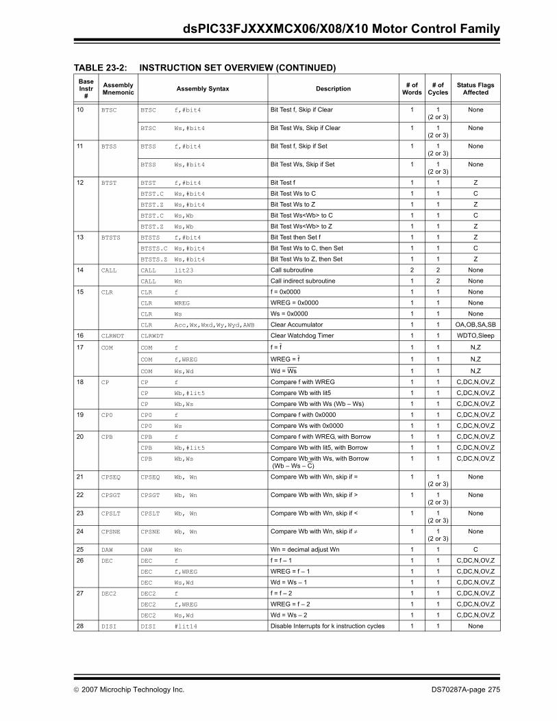
dsPIC33FJXXXMCX06/X08/X10 Motor Control Family
10 BTSC BTSC f,#bit4 Bit Test f, Skip if Clear 1 1 (2 or 3)
None
BTSC Ws,#bit4 Bit Test Ws, Skip if Clear 1 1 (2 or 3)
None
11 BTSS BTSS f,#bit4 Bit Test f, Skip if Set 1 1 (2 or 3)
None
BTSS Ws,#bit4 Bit Test Ws, Skip if Set 1 1 (2 or 3)
None
12 BTST BTST f,#bit4 Bit Test f 1 1 Z
BTST.C Ws,#bit4 Bit Test Ws to C 1 1 C
BTST.Z Ws,#bit4 Bit Test Ws to Z 1 1 Z
BTST.C Ws,Wb Bit Test Ws<Wb> to C 1 1 C
BTST.Z Ws,Wb Bit Test Ws<Wb> to Z 1 1 Z
13 BTSTS BTSTS f,#bit4 Bit Test then Set f 1 1 Z
BTSTS.C Ws,#bit4 Bit Test Ws to C, then Set 1 1 C
BTSTS.Z Ws,#bit4 Bit Test Ws to Z, then Set 1 1 Z
14 CALL CALL lit23 Call subroutine 2 2 None
CALL Wn Call indirect subroutine 1 2 None
15 CLR CLR f f = 0x0000 1 1 None
CLR WREG WREG = 0x0000 1 1 None
CLR Ws Ws = 0x0000 1 1 None
CLR Acc,Wx,Wxd,Wy,Wyd,AWB Clear Accumulator 1 1 OA,OB,SA,SB
16 CLRWDT CLRWDT Clear Watchdog Timer 1 1 WDTO,Sleep
17 COM COM f f = f 1 1 N,Z
COM f,WREG WREG = f 1 1 N,Z
COM Ws,Wd Wd = Ws 1 1 N,Z
18 CP CP f Compare f with WREG 1 1 C,DC,N,OV,Z
CP Wb,#lit5 Compare Wb with lit5 1 1 C,DC,N,OV,Z
CP Wb,Ws Compare Wb with Ws (Wb – Ws) 1 1 C,DC,N,OV,Z
19 CP0 CP0 f Compare f with 0x0000 1 1 C,DC,N,OV,Z
CP0 Ws Compare Ws with 0x0000 1 1 C,DC,N,OV,Z
20 CPB CPB f Compare f with WREG, with Borrow 1 1 C,DC,N,OV,Z
CPB Wb,#lit5 Compare Wb with lit5, with Borrow 1 1 C,DC,N,OV,Z
CPB Wb,Ws Compare Wb with Ws, with Borrow (Wb – Ws – C)
1 1 C,DC,N,OV,Z
21 CPSEQ CPSEQ Wb, Wn Compare Wb with Wn, skip if = 1 1 (2 or 3)
None
22 CPSGT CPSGT Wb, Wn Compare Wb with Wn, skip if > 1 1 (2 or 3)
None
23 CPSLT CPSLT Wb, Wn Compare Wb with Wn, skip if < 1 1 (2 or 3)
None
24 CPSNE CPSNE Wb, Wn Compare Wb with Wn, skip if ≠ 1 1 (2 or 3)
None
25 DAW DAW Wn Wn = decimal adjust Wn 1 1 C
26 DEC DEC f f = f – 1 1 1 C,DC,N,OV,Z
DEC f,WREG WREG = f – 1 1 1 C,DC,N,OV,Z
DEC Ws,Wd Wd = Ws – 1 1 1 C,DC,N,OV,Z
27 DEC2 DEC2 f f = f – 2 1 1 C,DC,N,OV,Z
DEC2 f,WREG WREG = f – 2 1 1 C,DC,N,OV,Z
DEC2 Ws,Wd Wd = Ws – 2 1 1 C,DC,N,OV,Z
28 DISI DISI #lit14 Disable Interrupts for k instruction cycles 1 1 None
TABLE 23-2: INSTRUCTION SET OVERVIEW (CONTINUED) BaseInstr
#AssemblyMnemonic Assembly Syntax Description # of
Words# of
CyclesStatus Flags
Affected
© 2007 Microchip Technology Inc. DS70287A-page 275
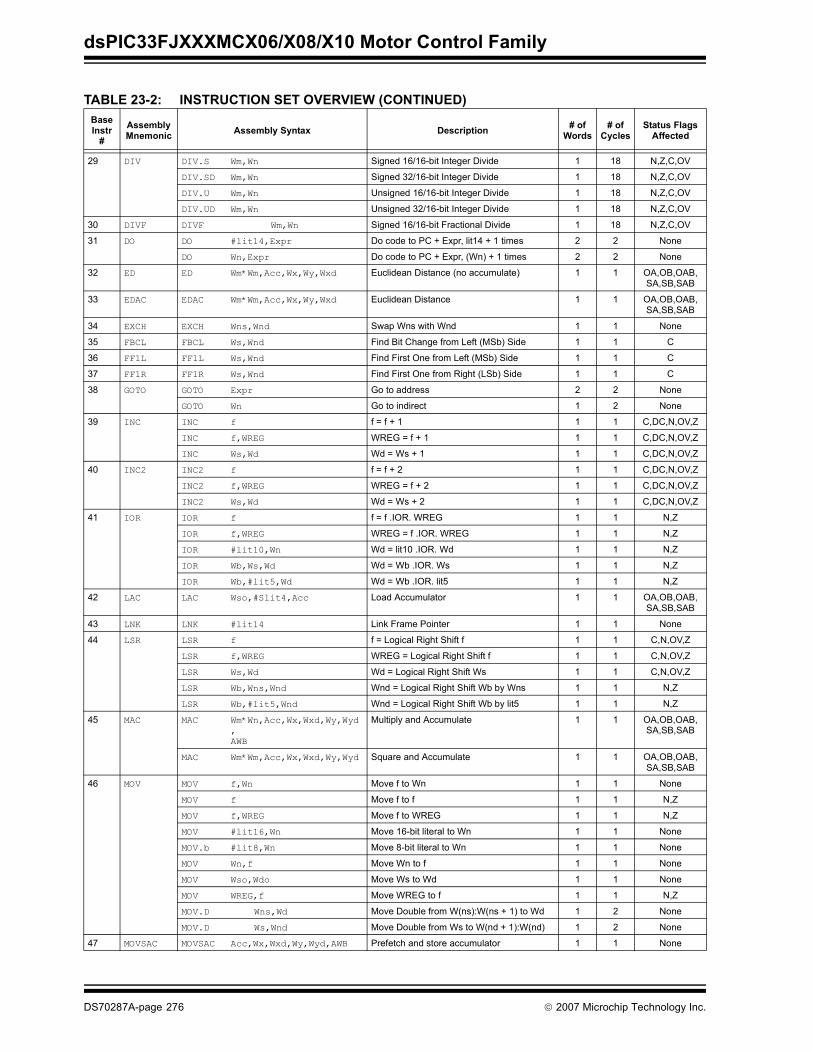
dsPIC33FJXXXMCX06/X08/X10 Motor Control Family
29 DIV DIV.S Wm,Wn Signed 16/16-bit Integer Divide 1 18 N,Z,C,OV
DIV.SD Wm,Wn Signed 32/16-bit Integer Divide 1 18 N,Z,C,OV
DIV.U Wm,Wn Unsigned 16/16-bit Integer Divide 1 18 N,Z,C,OV
DIV.UD Wm,Wn Unsigned 32/16-bit Integer Divide 1 18 N,Z,C,OV
30 DIVF DIVF Wm,Wn Signed 16/16-bit Fractional Divide 1 18 N,Z,C,OV
31 DO DO #lit14,Expr Do code to PC + Expr, lit14 + 1 times 2 2 None
DO Wn,Expr Do code to PC + Expr, (Wn) + 1 times 2 2 None
32 ED ED Wm*Wm,Acc,Wx,Wy,Wxd Euclidean Distance (no accumulate) 1 1 OA,OB,OAB,SA,SB,SAB
33 EDAC EDAC Wm*Wm,Acc,Wx,Wy,Wxd Euclidean Distance 1 1 OA,OB,OAB,SA,SB,SAB
34 EXCH EXCH Wns,Wnd Swap Wns with Wnd 1 1 None
35 FBCL FBCL Ws,Wnd Find Bit Change from Left (MSb) Side 1 1 C
36 FF1L FF1L Ws,Wnd Find First One from Left (MSb) Side 1 1 C
37 FF1R FF1R Ws,Wnd Find First One from Right (LSb) Side 1 1 C
38 GOTO GOTO Expr Go to address 2 2 None
GOTO Wn Go to indirect 1 2 None
39 INC INC f f = f + 1 1 1 C,DC,N,OV,Z
INC f,WREG WREG = f + 1 1 1 C,DC,N,OV,Z
INC Ws,Wd Wd = Ws + 1 1 1 C,DC,N,OV,Z
40 INC2 INC2 f f = f + 2 1 1 C,DC,N,OV,Z
INC2 f,WREG WREG = f + 2 1 1 C,DC,N,OV,Z
INC2 Ws,Wd Wd = Ws + 2 1 1 C,DC,N,OV,Z
41 IOR IOR f f = f .IOR. WREG 1 1 N,Z
IOR f,WREG WREG = f .IOR. WREG 1 1 N,Z
IOR #lit10,Wn Wd = lit10 .IOR. Wd 1 1 N,Z
IOR Wb,Ws,Wd Wd = Wb .IOR. Ws 1 1 N,Z
IOR Wb,#lit5,Wd Wd = Wb .IOR. lit5 1 1 N,Z
42 LAC LAC Wso,#Slit4,Acc Load Accumulator 1 1 OA,OB,OAB,SA,SB,SAB
43 LNK LNK #lit14 Link Frame Pointer 1 1 None
44 LSR LSR f f = Logical Right Shift f 1 1 C,N,OV,Z
LSR f,WREG WREG = Logical Right Shift f 1 1 C,N,OV,Z
LSR Ws,Wd Wd = Logical Right Shift Ws 1 1 C,N,OV,Z
LSR Wb,Wns,Wnd Wnd = Logical Right Shift Wb by Wns 1 1 N,Z
LSR Wb,#lit5,Wnd Wnd = Logical Right Shift Wb by lit5 1 1 N,Z
45 MAC MAC Wm*Wn,Acc,Wx,Wxd,Wy,Wyd,AWB
Multiply and Accumulate 1 1 OA,OB,OAB,SA,SB,SAB
MAC Wm*Wm,Acc,Wx,Wxd,Wy,Wyd Square and Accumulate 1 1 OA,OB,OAB,SA,SB,SAB
46 MOV MOV f,Wn Move f to Wn 1 1 None
MOV f Move f to f 1 1 N,Z
MOV f,WREG Move f to WREG 1 1 N,Z
MOV #lit16,Wn Move 16-bit literal to Wn 1 1 None
MOV.b #lit8,Wn Move 8-bit literal to Wn 1 1 None
MOV Wn,f Move Wn to f 1 1 None
MOV Wso,Wdo Move Ws to Wd 1 1 None
MOV WREG,f Move WREG to f 1 1 N,Z
MOV.D Wns,Wd Move Double from W(ns):W(ns + 1) to Wd 1 2 None
MOV.D Ws,Wnd Move Double from Ws to W(nd + 1):W(nd) 1 2 None
47 MOVSAC MOVSAC Acc,Wx,Wxd,Wy,Wyd,AWB Prefetch and store accumulator 1 1 None
TABLE 23-2: INSTRUCTION SET OVERVIEW (CONTINUED) BaseInstr
#AssemblyMnemonic Assembly Syntax Description # of
Words# of
CyclesStatus Flags
Affected
DS70287A-page 276 © 2007 Microchip Technology Inc.
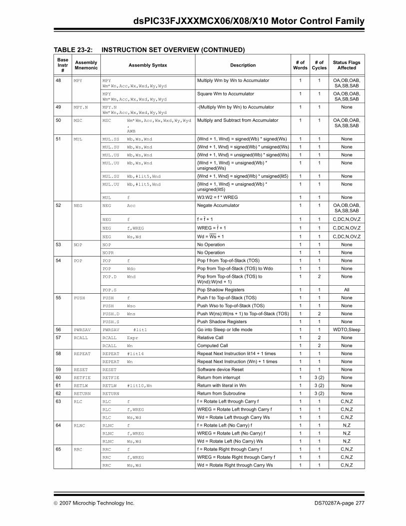
dsPIC33FJXXXMCX06/X08/X10 Motor Control Family
48 MPY MPY Wm*Wn,Acc,Wx,Wxd,Wy,Wyd
Multiply Wm by Wn to Accumulator 1 1 OA,OB,OAB,SA,SB,SAB
MPY Wm*Wm,Acc,Wx,Wxd,Wy,Wyd
Square Wm to Accumulator 1 1 OA,OB,OAB,SA,SB,SAB
49 MPY.N MPY.N Wm*Wn,Acc,Wx,Wxd,Wy,Wyd
-(Multiply Wm by Wn) to Accumulator 1 1 None
50 MSC MSC Wm*Wm,Acc,Wx,Wxd,Wy,Wyd,AWB
Multiply and Subtract from Accumulator 1 1 OA,OB,OAB,SA,SB,SAB
51 MUL MUL.SS Wb,Ws,Wnd {Wnd + 1, Wnd} = signed(Wb) * signed(Ws) 1 1 None
MUL.SU Wb,Ws,Wnd {Wnd + 1, Wnd} = signed(Wb) * unsigned(Ws) 1 1 None
MUL.US Wb,Ws,Wnd {Wnd + 1, Wnd} = unsigned(Wb) * signed(Ws) 1 1 None
MUL.UU Wb,Ws,Wnd {Wnd + 1, Wnd} = unsigned(Wb) * unsigned(Ws)
1 1 None
MUL.SU Wb,#lit5,Wnd {Wnd + 1, Wnd} = signed(Wb) * unsigned(lit5) 1 1 None
MUL.UU Wb,#lit5,Wnd {Wnd + 1, Wnd} = unsigned(Wb) * unsigned(lit5)
1 1 None
MUL f W3:W2 = f * WREG 1 1 None
52 NEG NEG Acc Negate Accumulator 1 1 OA,OB,OAB,SA,SB,SAB
NEG f f = f + 1 1 1 C,DC,N,OV,Z
NEG f,WREG WREG = f + 1 1 1 C,DC,N,OV,Z
NEG Ws,Wd Wd = Ws + 1 1 1 C,DC,N,OV,Z
53 NOP NOP No Operation 1 1 None
NOPR No Operation 1 1 None
54 POP POP f Pop f from Top-of-Stack (TOS) 1 1 None
POP Wdo Pop from Top-of-Stack (TOS) to Wdo 1 1 None
POP.D Wnd Pop from Top-of-Stack (TOS) to W(nd):W(nd + 1)
1 2 None
POP.S Pop Shadow Registers 1 1 All
55 PUSH PUSH f Push f to Top-of-Stack (TOS) 1 1 None
PUSH Wso Push Wso to Top-of-Stack (TOS) 1 1 None
PUSH.D Wns Push W(ns):W(ns + 1) to Top-of-Stack (TOS) 1 2 None
PUSH.S Push Shadow Registers 1 1 None
56 PWRSAV PWRSAV #lit1 Go into Sleep or Idle mode 1 1 WDTO,Sleep
57 RCALL RCALL Expr Relative Call 1 2 None
RCALL Wn Computed Call 1 2 None
58 REPEAT REPEAT #lit14 Repeat Next Instruction lit14 + 1 times 1 1 None
REPEAT Wn Repeat Next Instruction (Wn) + 1 times 1 1 None
59 RESET RESET Software device Reset 1 1 None
60 RETFIE RETFIE Return from interrupt 1 3 (2) None
61 RETLW RETLW #lit10,Wn Return with literal in Wn 1 3 (2) None
62 RETURN RETURN Return from Subroutine 1 3 (2) None
63 RLC RLC f f = Rotate Left through Carry f 1 1 C,N,Z
RLC f,WREG WREG = Rotate Left through Carry f 1 1 C,N,Z
RLC Ws,Wd Wd = Rotate Left through Carry Ws 1 1 C,N,Z
64 RLNC RLNC f f = Rotate Left (No Carry) f 1 1 N,Z
RLNC f,WREG WREG = Rotate Left (No Carry) f 1 1 N,Z
RLNC Ws,Wd Wd = Rotate Left (No Carry) Ws 1 1 N,Z
65 RRC RRC f f = Rotate Right through Carry f 1 1 C,N,Z
RRC f,WREG WREG = Rotate Right through Carry f 1 1 C,N,Z
RRC Ws,Wd Wd = Rotate Right through Carry Ws 1 1 C,N,Z
TABLE 23-2: INSTRUCTION SET OVERVIEW (CONTINUED) BaseInstr
#AssemblyMnemonic Assembly Syntax Description # of
Words# of
CyclesStatus Flags
Affected
© 2007 Microchip Technology Inc. DS70287A-page 277
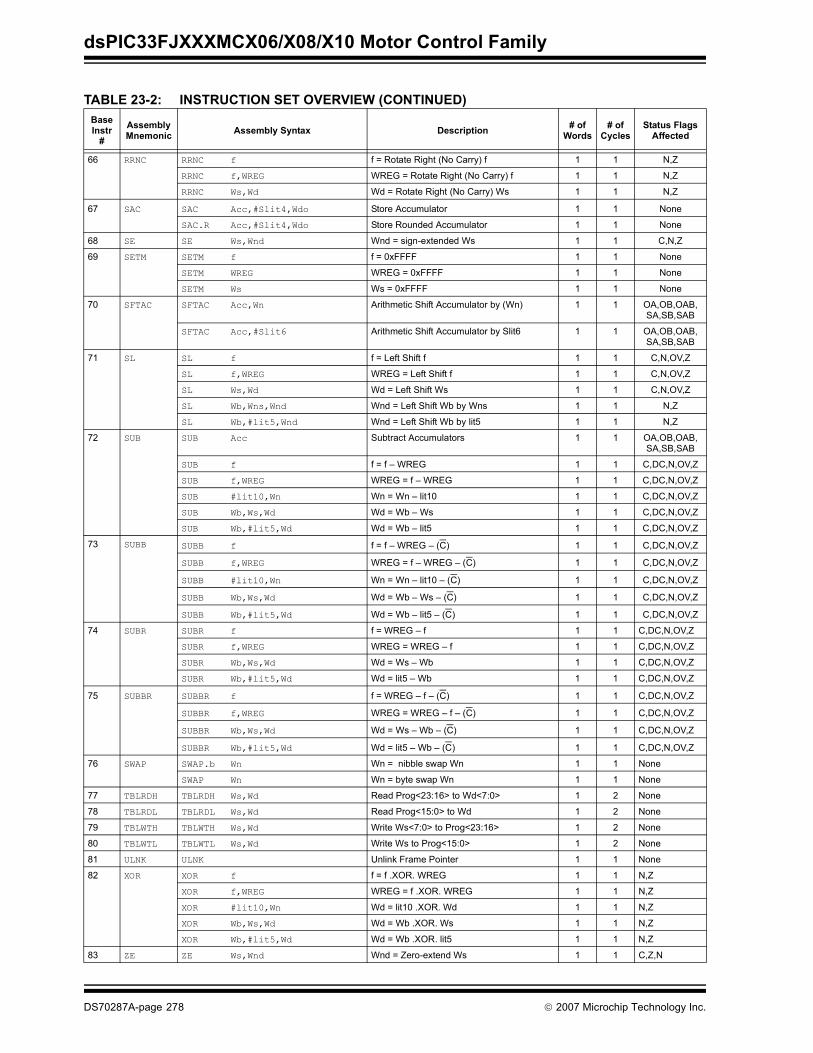
dsPIC33FJXXXMCX06/X08/X10 Motor Control Family
66 RRNC RRNC f f = Rotate Right (No Carry) f 1 1 N,Z
RRNC f,WREG WREG = Rotate Right (No Carry) f 1 1 N,Z
RRNC Ws,Wd Wd = Rotate Right (No Carry) Ws 1 1 N,Z
67 SAC SAC Acc,#Slit4,Wdo Store Accumulator 1 1 None
SAC.R Acc,#Slit4,Wdo Store Rounded Accumulator 1 1 None
68 SE SE Ws,Wnd Wnd = sign-extended Ws 1 1 C,N,Z
69 SETM SETM f f = 0xFFFF 1 1 None
SETM WREG WREG = 0xFFFF 1 1 None
SETM Ws Ws = 0xFFFF 1 1 None
70 SFTAC SFTAC Acc,Wn Arithmetic Shift Accumulator by (Wn) 1 1 OA,OB,OAB,SA,SB,SAB
SFTAC Acc,#Slit6 Arithmetic Shift Accumulator by Slit6 1 1 OA,OB,OAB,SA,SB,SAB
71 SL SL f f = Left Shift f 1 1 C,N,OV,Z
SL f,WREG WREG = Left Shift f 1 1 C,N,OV,Z
SL Ws,Wd Wd = Left Shift Ws 1 1 C,N,OV,Z
SL Wb,Wns,Wnd Wnd = Left Shift Wb by Wns 1 1 N,Z
SL Wb,#lit5,Wnd Wnd = Left Shift Wb by lit5 1 1 N,Z
72 SUB SUB Acc Subtract Accumulators 1 1 OA,OB,OAB,SA,SB,SAB
SUB f f = f – WREG 1 1 C,DC,N,OV,Z
SUB f,WREG WREG = f – WREG 1 1 C,DC,N,OV,Z
SUB #lit10,Wn Wn = Wn – lit10 1 1 C,DC,N,OV,Z
SUB Wb,Ws,Wd Wd = Wb – Ws 1 1 C,DC,N,OV,Z
SUB Wb,#lit5,Wd Wd = Wb – lit5 1 1 C,DC,N,OV,Z
73 SUBB SUBB f f = f – WREG – (C) 1 1 C,DC,N,OV,Z
SUBB f,WREG WREG = f – WREG – (C) 1 1 C,DC,N,OV,Z
SUBB #lit10,Wn Wn = Wn – lit10 – (C) 1 1 C,DC,N,OV,Z
SUBB Wb,Ws,Wd Wd = Wb – Ws – (C) 1 1 C,DC,N,OV,Z
SUBB Wb,#lit5,Wd Wd = Wb – lit5 – (C) 1 1 C,DC,N,OV,Z
74 SUBR SUBR f f = WREG – f 1 1 C,DC,N,OV,Z
SUBR f,WREG WREG = WREG – f 1 1 C,DC,N,OV,Z
SUBR Wb,Ws,Wd Wd = Ws – Wb 1 1 C,DC,N,OV,Z
SUBR Wb,#lit5,Wd Wd = lit5 – Wb 1 1 C,DC,N,OV,Z
75 SUBBR SUBBR f f = WREG – f – (C) 1 1 C,DC,N,OV,Z
SUBBR f,WREG WREG = WREG – f – (C) 1 1 C,DC,N,OV,Z
SUBBR Wb,Ws,Wd Wd = Ws – Wb – (C) 1 1 C,DC,N,OV,Z
SUBBR Wb,#lit5,Wd Wd = lit5 – Wb – (C) 1 1 C,DC,N,OV,Z
76 SWAP SWAP.b Wn Wn = nibble swap Wn 1 1 None
SWAP Wn Wn = byte swap Wn 1 1 None
77 TBLRDH TBLRDH Ws,Wd Read Prog<23:16> to Wd<7:0> 1 2 None
78 TBLRDL TBLRDL Ws,Wd Read Prog<15:0> to Wd 1 2 None
79 TBLWTH TBLWTH Ws,Wd Write Ws<7:0> to Prog<23:16> 1 2 None
80 TBLWTL TBLWTL Ws,Wd Write Ws to Prog<15:0> 1 2 None
81 ULNK ULNK Unlink Frame Pointer 1 1 None
82 XOR XOR f f = f .XOR. WREG 1 1 N,Z
XOR f,WREG WREG = f .XOR. WREG 1 1 N,Z
XOR #lit10,Wn Wd = lit10 .XOR. Wd 1 1 N,Z
XOR Wb,Ws,Wd Wd = Wb .XOR. Ws 1 1 N,Z
XOR Wb,#lit5,Wd Wd = Wb .XOR. lit5 1 1 N,Z
83 ZE ZE Ws,Wnd Wnd = Zero-extend Ws 1 1 C,Z,N
TABLE 23-2: INSTRUCTION SET OVERVIEW (CONTINUED) BaseInstr
#AssemblyMnemonic Assembly Syntax Description # of
Words# of
CyclesStatus Flags
Affected
DS70287A-page 278 © 2007 Microchip Technology Inc.
dsPIC33FJXXXMCX06/X08/X10 MOTOR CONTROL FAMILY
24.0 DEVELOPMENT SUPPORTThe PIC® microcontrollers are supported with a fullrange of hardware and software development tools:
• Integrated Development Environment- MPLAB® IDE Software
• Assemblers/Compilers/Linkers- MPASMTM Assembler- MPLAB C18 and MPLAB C30 C Compilers- MPLINKTM Object Linker/
MPLIBTM Object Librarian- MPLAB ASM30 Assembler/Linker/Library
• Simulators- MPLAB SIM Software Simulator
• Emulators- MPLAB ICE 2000 In-Circuit Emulator- MPLAB REAL ICE™ In-Circuit Emulator
• In-Circuit Debugger- MPLAB ICD 2
• Device Programmers- PICSTART® Plus Development Programmer- MPLAB PM3 Device Programmer- PICkit™ 2 Development Programmer
• Low-Cost Demonstration and Development Boards and Evaluation Kits
24.1 MPLAB Integrated Development Environment Software
The MPLAB IDE software brings an ease of softwaredevelopment previously unseen in the 8/16-bit micro-controller market. The MPLAB IDE is a Windows®
operating system-based application that contains:
• A single graphical interface to all debugging tools- Simulator- Programmer (sold separately)- Emulator (sold separately)- In-Circuit Debugger (sold separately)
• A full-featured editor with color-coded context• A multiple project manager• Customizable data windows with direct edit of
contents• High-level source code debugging• Visual device initializer for easy register
initialization• Mouse over variable inspection• Drag and drop variables from source to watch
windows• Extensive on-line help• Integration of select third party tools, such as
HI-TECH Software C Compilers and IAR C Compilers
The MPLAB IDE allows you to:
• Edit your source files (either assembly or C)• One touch assemble (or compile) and download
to PIC MCU emulator and simulator tools (automatically updates all project information)
• Debug using:- Source files (assembly or C)- Mixed assembly and C- Machine code
MPLAB IDE supports multiple debugging tools in asingle development paradigm, from the cost-effectivesimulators, through low-cost in-circuit debuggers, tofull-featured emulators. This eliminates the learningcurve when upgrading to tools with increased flexibilityand power.
© 2007 Microchip Technology Inc. DS70287A-page 279
dsPIC33FJXXXMCX06/X08/X10 MOTOR CONTROL FAMILY
24.2 MPASM AssemblerThe MPASM Assembler is a full-featured, universalmacro assembler for all PIC MCUs.
The MPASM Assembler generates relocatable objectfiles for the MPLINK Object Linker, Intel® standard HEXfiles, MAP files to detail memory usage and symbolreference, absolute LST files that contain source linesand generated machine code and COFF files fordebugging.
The MPASM Assembler features include:
• Integration into MPLAB IDE projects• User-defined macros to streamline
assembly code• Conditional assembly for multi-purpose
source files• Directives that allow complete control over the
assembly process
24.3 MPLAB C18 and MPLAB C30 C Compilers
The MPLAB C18 and MPLAB C30 Code DevelopmentSystems are complete ANSI C compilers forMicrochip’s PIC18 and PIC24 families of microcontrol-lers and the dsPIC30 and dsPIC33 family of digital sig-nal controllers. These compilers provide powerfulintegration capabilities, superior code optimization andease of use not found with other compilers.
For easy source level debugging, the compilers providesymbol information that is optimized to the MPLAB IDEdebugger.
24.4 MPLINK Object Linker/MPLIB Object Librarian
The MPLINK Object Linker combines relocatableobjects created by the MPASM Assembler and theMPLAB C18 C Compiler. It can link relocatable objectsfrom precompiled libraries, using directives from alinker script.
The MPLIB Object Librarian manages the creation andmodification of library files of precompiled code. Whena routine from a library is called from a source file, onlythe modules that contain that routine will be linked inwith the application. This allows large libraries to beused efficiently in many different applications.
The object linker/library features include:
• Efficient linking of single libraries instead of many smaller files
• Enhanced code maintainability by grouping related modules together
• Flexible creation of libraries with easy module listing, replacement, deletion and extraction
24.5 MPLAB ASM30 Assembler, Linker and Librarian
MPLAB ASM30 Assembler produces relocatablemachine code from symbolic assembly language fordsPIC30F devices. MPLAB C30 C Compiler uses theassembler to produce its object file. The assemblergenerates relocatable object files that can then bearchived or linked with other relocatable object files andarchives to create an executable file. Notable featuresof the assembler include:
• Support for the entire dsPIC30F instruction set• Support for fixed-point and floating-point data• Command line interface• Rich directive set• Flexible macro language• MPLAB IDE compatibility
24.6 MPLAB SIM Software SimulatorThe MPLAB SIM Software Simulator allows codedevelopment in a PC-hosted environment by simulat-ing the PIC MCUs and dsPIC® DSCs on an instructionlevel. On any given instruction, the data areas can beexamined or modified and stimuli can be applied froma comprehensive stimulus controller. Registers can belogged to files for further run-time analysis. The tracebuffer and logic analyzer display extend the power ofthe simulator to record and track program execution,actions on I/O, most peripherals and internal registers.
The MPLAB SIM Software Simulator fully supportssymbolic debugging using the MPLAB C18 andMPLAB C30 C Compilers, and the MPASM andMPLAB ASM30 Assemblers. The software simulatoroffers the flexibility to develop and debug code outsideof the hardware laboratory environment, making it anexcellent, economical software development tool.
DS70287A-page 280 © 2007 Microchip Technology Inc.
dsPIC33FJXXXMCX06/X08/X10 MOTOR CONTROL FAMILY
24.7 MPLAB ICE 2000 High-Performance In-Circuit Emulator
The MPLAB ICE 2000 In-Circuit Emulator is intendedto provide the product development engineer with acomplete microcontroller design tool set for PICmicrocontrollers. Software control of the MPLAB ICE2000 In-Circuit Emulator is advanced by the MPLABIntegrated Development Environment, which allowsediting, building, downloading and source debuggingfrom a single environment.
The MPLAB ICE 2000 is a full-featured emulatorsystem with enhanced trace, trigger and data monitor-ing features. Interchangeable processor modules allowthe system to be easily reconfigured for emulation ofdifferent processors. The architecture of the MPLABICE 2000 In-Circuit Emulator allows expansion tosupport new PIC microcontrollers.
The MPLAB ICE 2000 In-Circuit Emulator system hasbeen designed as a real-time emulation system withadvanced features that are typically found on moreexpensive development tools. The PC platform andMicrosoft® Windows® 32-bit operating system werechosen to best make these features available in asimple, unified application.
24.8 MPLAB REAL ICE In-Circuit Emulator System
MPLAB REAL ICE In-Circuit Emulator System isMicrochip’s next generation high-speed emulator forMicrochip Flash DSC and MCU devices. It debugs andprograms PIC® Flash MCUs and dsPIC® Flash DSCswith the easy-to-use, powerful graphical user interface ofthe MPLAB Integrated Development Environment (IDE),included with each kit.
The MPLAB REAL ICE probe is connected to the designengineer’s PC using a high-speed USB 2.0 interface andis connected to the target with either a connectorcompatible with the popular MPLAB ICD 2 system(RJ11) or with the new high-speed, noise tolerant, Low-Voltage Differential Signal (LVDS) interconnection(CAT5).
MPLAB REAL ICE is field upgradeable through futurefirmware downloads in MPLAB IDE. In upcomingreleases of MPLAB IDE, new devices will be supported,and new features will be added, such as software break-points and assembly code trace. MPLAB REAL ICEoffers significant advantages over competitive emulatorsincluding low-cost, full-speed emulation, real-timevariable watches, trace analysis, complex breakpoints, aruggedized probe interface and long (up to three meters)interconnection cables.
24.9 MPLAB ICD 2 In-Circuit DebuggerMicrochip’s In-Circuit Debugger, MPLAB ICD 2, is apowerful, low-cost, run-time development tool,connecting to the host PC via an RS-232 or high-speedUSB interface. This tool is based on the Flash PICMCUs and can be used to develop for these and otherPIC MCUs and dsPIC DSCs. The MPLAB ICD 2 utilizesthe in-circuit debugging capability built into the Flashdevices. This feature, along with Microchip’s In-CircuitSerial ProgrammingTM (ICSPTM) protocol, offers cost-effective, in-circuit Flash debugging from the graphicaluser interface of the MPLAB Integrated DevelopmentEnvironment. This enables a designer to develop anddebug source code by setting breakpoints, single step-ping and watching variables, and CPU status andperipheral registers. Running at full speed enablestesting hardware and applications in real time. MPLABICD 2 also serves as a development programmer forselected PIC devices.
24.10 MPLAB PM3 Device ProgrammerThe MPLAB PM3 Device Programmer is a universal,CE compliant device programmer with programmablevoltage verification at VDDMIN and VDDMAX formaximum reliability. It features a large LCD display(128 x 64) for menus and error messages and a modu-lar, detachable socket assembly to support variouspackage types. The ICSP™ cable assembly is includedas a standard item. In Stand-Alone mode, the MPLABPM3 Device Programmer can read, verify and programPIC devices without a PC connection. It can also setcode protection in this mode. The MPLAB PM3connects to the host PC via an RS-232 or USB cable.The MPLAB PM3 has high-speed communications andoptimized algorithms for quick programming of largememory devices and incorporates an SD/MMC card forfile storage and secure data applications.
© 2007 Microchip Technology Inc. DS70287A-page 281
dsPIC33FJXXXMCX06/X08/X10 MOTOR CONTROL FAMILY
24.11 PICSTART Plus Development Programmer
The PICSTART Plus Development Programmer is aneasy-to-use, low-cost, prototype programmer. Itconnects to the PC via a COM (RS-232) port. MPLABIntegrated Development Environment software makesusing the programmer simple and efficient. ThePICSTART Plus Development Programmer supportsmost PIC devices in DIP packages up to 40 pins.Larger pin count devices, such as the PIC16C92X andPIC17C76X, may be supported with an adapter socket.The PICSTART Plus Development Programmer is CEcompliant.
24.12 PICkit 2 Development ProgrammerThe PICkit™ 2 Development Programmer is a low-costprogrammer and selected Flash device debugger withan easy-to-use interface for programming many ofMicrochip’s baseline, mid-range and PIC18F families ofFlash memory microcontrollers. The PICkit 2 Starter Kitincludes a prototyping development board, twelvesequential lessons, software and HI-TECH’s PICC™Lite C compiler, and is designed to help get up to speedquickly using PIC® microcontrollers. The kit provideseverything needed to program, evaluate and developapplications using Microchip’s powerful, mid-rangeFlash memory family of microcontrollers.
24.13 Demonstration, Development and Evaluation Boards
A wide variety of demonstration, development andevaluation boards for various PIC MCUs and dsPICDSCs allows quick application development on fully func-tional systems. Most boards include prototyping areas foradding custom circuitry and provide application firmwareand source code for examination and modification.
The boards support a variety of features, including LEDs,temperature sensors, switches, speakers, RS-232interfaces, LCD displays, potentiometers and additionalEEPROM memory.
The demonstration and development boards can beused in teaching environments, for prototyping customcircuits and for learning about various microcontrollerapplications.
In addition to the PICDEM™ and dsPICDEM™ demon-stration/development board series of circuits, Microchiphas a line of evaluation kits and demonstration softwarefor analog filter design, KEELOQ® security ICs, CAN,IrDA®, PowerSmart battery management, SEEVAL®
evaluation system, Sigma-Delta ADC, flow ratesensing, plus many more.
Check the Microchip web page (www.microchip.com)for the complete list of demonstration, developmentand evaluation kits.
DS70287A-page 282 © 2007 Microchip Technology Inc.

dsPIC33FJXXXMCX06/X08/X10 MOTOR CONTROL FAMILY
25.0 ELECTRICAL CHARACTERISTICSThis section provides an overview of dsPIC33FJXXXMCX06/X08/X10 Motor Control Family electrical characteristics.Additional information will be provided in future revisions of this document as it becomes available.
Absolute maximum ratings for the dsPIC33FJXXXMCX06/X08/X10 Motor Control Family family are listed below. Expo-sure to these maximum rating conditions for extended periods may affect device reliability. Functional operation of thedevice at these or any other conditions above the parameters indicated in the operation listings of this specification isnot implied.
Absolute Maximum Ratings(1) Ambient temperature under bias.............................................................................................................. .-40°C to +85°CStorage temperature .............................................................................................................................. -65°C to +150°CVoltage on VDD with respect to VSS ......................................................................................................... -0.3V to +4.0VVoltage on any combined analog and digital pin and MCLR, with respect to VSS ......................... -0.3V to (VDD + 0.3V)Voltage on any digital-only pin with respect to VSS .................................................................................. -0.3V to +5.6VVoltage on VDDCORE with respect to VSS ................................................................................................ 2.25V to 2.75VMaximum current out of VSS pin ...........................................................................................................................300 mAMaximum current into VDD pin(2)...........................................................................................................................250 mAMaximum output current sunk by any I/O pin(3) ........................................................................................................4 mAMaximum output current sourced by any I/O pin(3)...................................................................................................4 mAMaximum current sunk by all ports .......................................................................................................................200 mAMaximum current sourced by all ports(2)...............................................................................................................200 mA
Note 1: Stresses above those listed under “Absolute Maximum Ratings” may cause permanent damage to thedevice. This is a stress rating only and functional operation of the device at those or any other conditionsabove those indicated in the operation listings of this specification is not implied. Exposure to maximumrating conditions for extended periods may affect device reliability.
2: Maximum allowable current is a function of device maximum power dissipation (see Table 25-2).
3: Exceptions are CLKOUT, which is able to sink/source 25 mA, and the VREF+, VREF-, SCLx, SDAx, PGCxand PGDx pins, which are able to sink/source 12 mA.
© 2007 Microchip Technology Inc. DS70287A-page 283
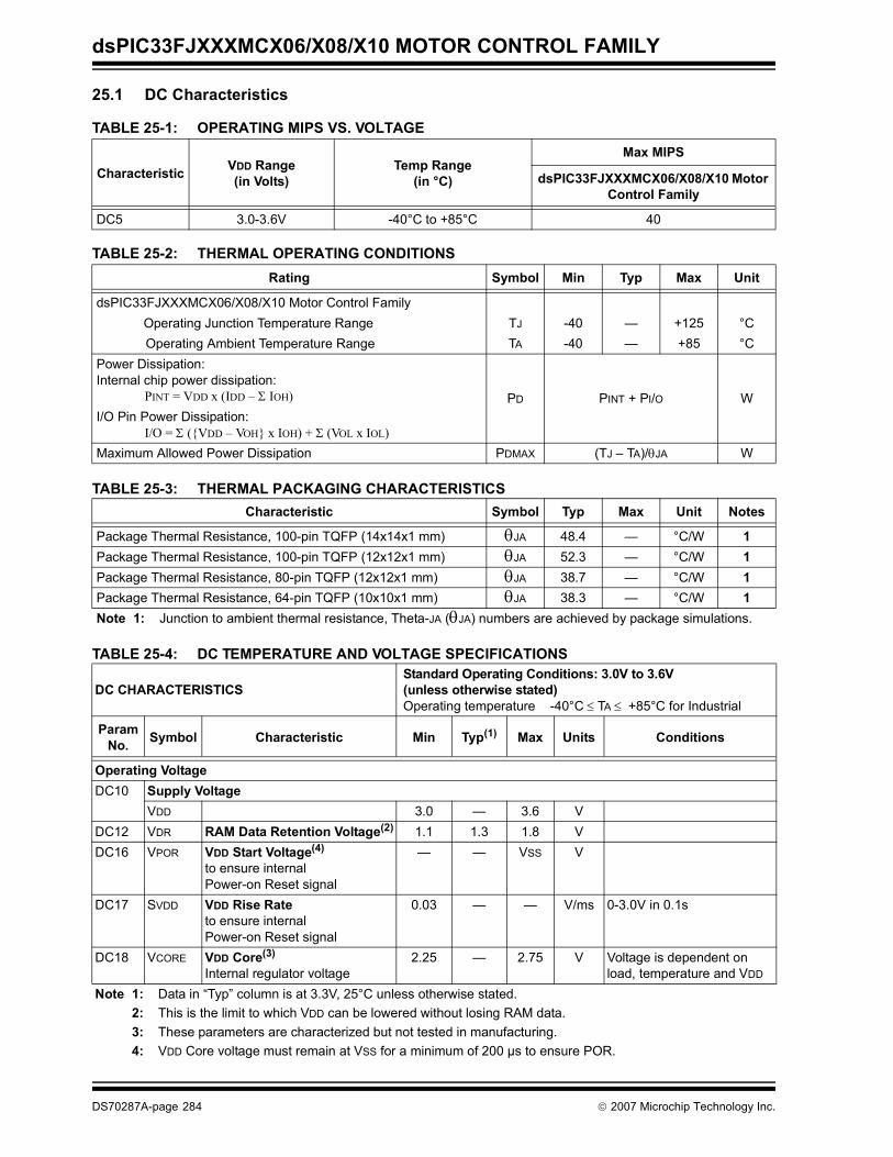
dsPIC33FJXXXMCX06/X08/X10 MOTOR CONTROL FAMILY
25.1 DC Characteristics
TABLE 25-1: OPERATING MIPS VS. VOLTAGE
Characteristic VDD Range(in Volts)
Temp Range(in °C)
Max MIPS
dsPIC33FJXXXMCX06/X08/X10 Motor Control Family
DC5 3.0-3.6V -40°C to +85°C 40
TABLE 25-2: THERMAL OPERATING CONDITIONSRating Symbol Min Typ Max Unit
dsPIC33FJXXXMCX06/X08/X10 Motor Control FamilyOperating Junction Temperature Range TJ -40 — +125 °COperating Ambient Temperature Range TA -40 — +85 °C
Power Dissipation:Internal chip power dissipation:
PINT = VDD x (IDD – Σ IOH) PD PINT + PI/O WI/O Pin Power Dissipation:
I/O = Σ ({VDD – VOH} x IOH) + Σ (VOL x IOL) Maximum Allowed Power Dissipation PDMAX (TJ – TA)/θJA W
TABLE 25-3: THERMAL PACKAGING CHARACTERISTICSCharacteristic Symbol Typ Max Unit Notes
Package Thermal Resistance, 100-pin TQFP (14x14x1 mm) θJA 48.4 — °C/W 1Package Thermal Resistance, 100-pin TQFP (12x12x1 mm) θJA 52.3 — °C/W 1Package Thermal Resistance, 80-pin TQFP (12x12x1 mm) θJA 38.7 — °C/W 1Package Thermal Resistance, 64-pin TQFP (10x10x1 mm) θJA 38.3 — °C/W 1Note 1: Junction to ambient thermal resistance, Theta-JA (θJA) numbers are achieved by package simulations.
TABLE 25-4: DC TEMPERATURE AND VOLTAGE SPECIFICATIONS
DC CHARACTERISTICSStandard Operating Conditions: 3.0V to 3.6V(unless otherwise stated)Operating temperature -40°C ≤ TA ≤ +85°C for Industrial
Param No. Symbol Characteristic Min Typ(1) Max Units Conditions
Operating VoltageDC10 Supply Voltage
VDD 3.0 — 3.6 VDC12 VDR RAM Data Retention Voltage(2) 1.1 1.3 1.8 VDC16 VPOR VDD Start Voltage(4)
to ensure internal Power-on Reset signal
— — VSS V
DC17 SVDD VDD Rise Rateto ensure internalPower-on Reset signal
0.03 — — V/ms 0-3.0V in 0.1s
DC18 VCORE VDD Core(3) Internal regulator voltage
2.25 — 2.75 V Voltage is dependent on load, temperature and VDD
Note 1: Data in “Typ” column is at 3.3V, 25°C unless otherwise stated.2: This is the limit to which VDD can be lowered without losing RAM data.3: These parameters are characterized but not tested in manufacturing.4: VDD Core voltage must remain at VSS for a minimum of 200 µs to ensure POR.
DS70287A-page 284 © 2007 Microchip Technology Inc.
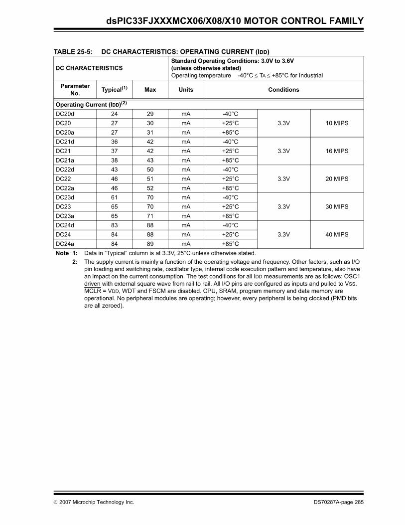
dsPIC33FJXXXMCX06/X08/X10 MOTOR CONTROL FAMILY
TABLE 25-5: DC CHARACTERISTICS: OPERATING CURRENT (IDD)
DC CHARACTERISTICSStandard Operating Conditions: 3.0V to 3.6V(unless otherwise stated)Operating temperature -40°C ≤ TA ≤ +85°C for Industrial
Parameter No. Typical(1) Max Units Conditions
Operating Current (IDD)(2)
DC20d 24 29 mA -40°C3.3V 10 MIPSDC20 27 30 mA +25°C
DC20a 27 31 mA +85°CDC21d 36 42 mA -40°C
3.3V 16 MIPSDC21 37 42 mA +25°CDC21a 38 43 mA +85°CDC22d 43 50 mA -40°C
3.3V 20 MIPSDC22 46 51 mA +25°CDC22a 46 52 mA +85°CDC23d 61 70 mA -40°C
3.3V 30 MIPSDC23 65 70 mA +25°CDC23a 65 71 mA +85°CDC24d 83 88 mA -40°C
3.3V 40 MIPSDC24 84 88 mA +25°CDC24a 84 89 mA +85°CNote 1: Data in “Typical” column is at 3.3V, 25°C unless otherwise stated.
2: The supply current is mainly a function of the operating voltage and frequency. Other factors, such as I/O pin loading and switching rate, oscillator type, internal code execution pattern and temperature, also have an impact on the current consumption. The test conditions for all IDD measurements are as follows: OSC1 driven with external square wave from rail to rail. All I/O pins are configured as inputs and pulled to VSS. MCLR = VDD, WDT and FSCM are disabled. CPU, SRAM, program memory and data memory are operational. No peripheral modules are operating; however, every peripheral is being clocked (PMD bits are all zeroed).
© 2007 Microchip Technology Inc. DS70287A-page 285
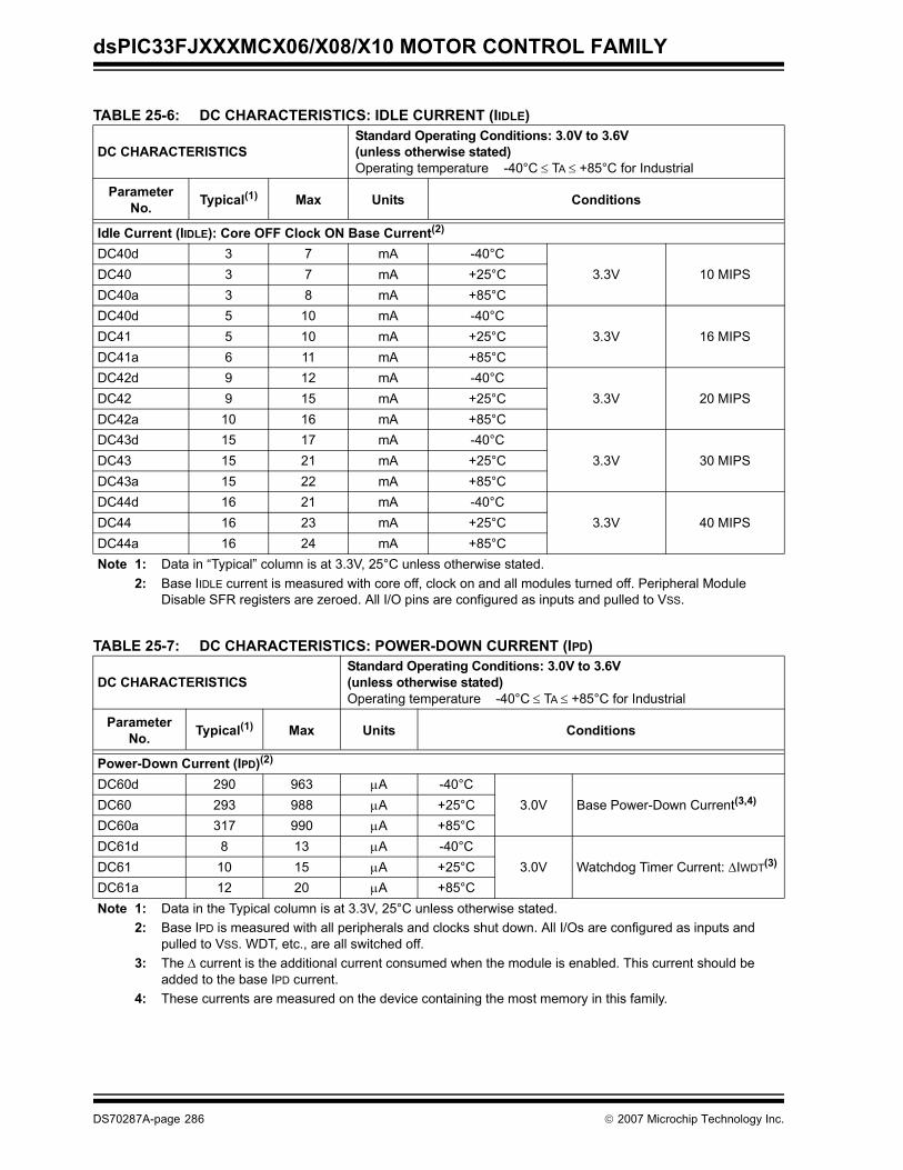
dsPIC33FJXXXMCX06/X08/X10 MOTOR CONTROL FAMILY
TABLE 25-6: DC CHARACTERISTICS: IDLE CURRENT (IIDLE)
DC CHARACTERISTICSStandard Operating Conditions: 3.0V to 3.6V(unless otherwise stated)Operating temperature -40°C ≤ TA ≤ +85°C for Industrial
Parameter No. Typical(1) Max Units Conditions
Idle Current (IIDLE): Core OFF Clock ON Base Current(2)
DC40d 3 7 mA -40°C3.3V 10 MIPSDC40 3 7 mA +25°C
DC40a 3 8 mA +85°CDC40d 5 10 mA -40°C
3.3V 16 MIPSDC41 5 10 mA +25°CDC41a 6 11 mA +85°CDC42d 9 12 mA -40°C
3.3V 20 MIPSDC42 9 15 mA +25°CDC42a 10 16 mA +85°CDC43d 15 17 mA -40°C
3.3V 30 MIPSDC43 15 21 mA +25°CDC43a 15 22 mA +85°CDC44d 16 21 mA -40°C
3.3V 40 MIPSDC44 16 23 mA +25°CDC44a 16 24 mA +85°CNote 1: Data in “Typical” column is at 3.3V, 25°C unless otherwise stated.
2: Base IIDLE current is measured with core off, clock on and all modules turned off. Peripheral Module Disable SFR registers are zeroed. All I/O pins are configured as inputs and pulled to VSS.
TABLE 25-7: DC CHARACTERISTICS: POWER-DOWN CURRENT (IPD)
DC CHARACTERISTICSStandard Operating Conditions: 3.0V to 3.6V(unless otherwise stated)Operating temperature -40°C ≤ TA ≤ +85°C for Industrial
Parameter No. Typical(1) Max Units Conditions
Power-Down Current (IPD)(2)
DC60d 290 963 μA -40°C3.0V Base Power-Down Current(3,4)DC60 293 988 μA +25°C
DC60a 317 990 μA +85°CDC61d 8 13 μA -40°C
3.0V Watchdog Timer Current: ΔIWDT(3)DC61 10 15 μA +25°CDC61a 12 20 μA +85°CNote 1: Data in the Typical column is at 3.3V, 25°C unless otherwise stated.
2: Base IPD is measured with all peripherals and clocks shut down. All I/Os are configured as inputs and pulled to VSS. WDT, etc., are all switched off.
3: The Δ current is the additional current consumed when the module is enabled. This current should be added to the base IPD current.
4: These currents are measured on the device containing the most memory in this family.
DS70287A-page 286 © 2007 Microchip Technology Inc.
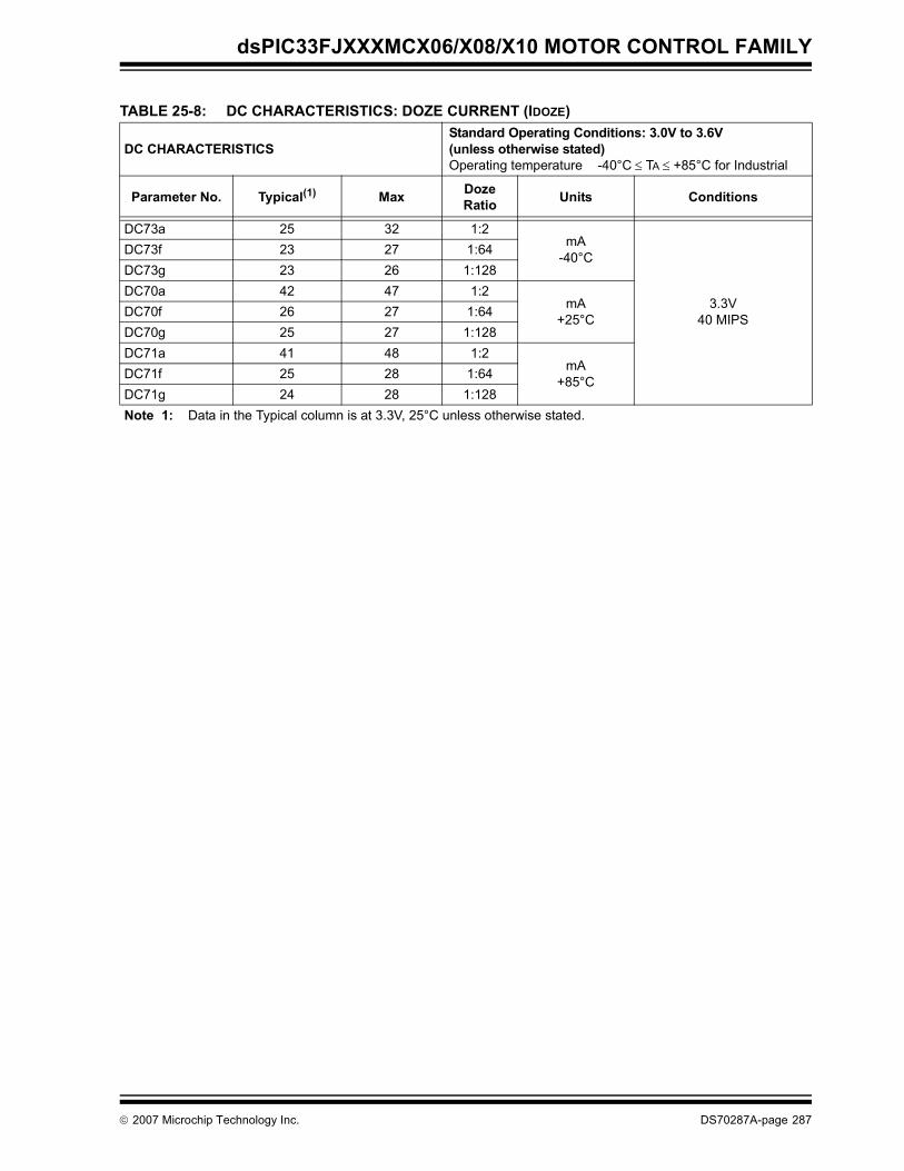
dsPIC33FJXXXMCX06/X08/X10 MOTOR CONTROL FAMILY
TABLE 25-8: DC CHARACTERISTICS: DOZE CURRENT (IDOZE)
DC CHARACTERISTICSStandard Operating Conditions: 3.0V to 3.6V(unless otherwise stated)Operating temperature -40°C ≤ TA ≤ +85°C for Industrial
Parameter No. Typical(1) Max Doze Ratio Units Conditions
DC73a 25 32 1:2mA
-40°C
3.3V40 MIPS
DC73f 23 27 1:64DC73g 23 26 1:128DC70a 42 47 1:2
mA+25°CDC70f 26 27 1:64
DC70g 25 27 1:128DC71a 41 48 1:2
mA+85°CDC71f 25 28 1:64
DC71g 24 28 1:128Note 1: Data in the Typical column is at 3.3V, 25°C unless otherwise stated.
© 2007 Microchip Technology Inc. DS70287A-page 287
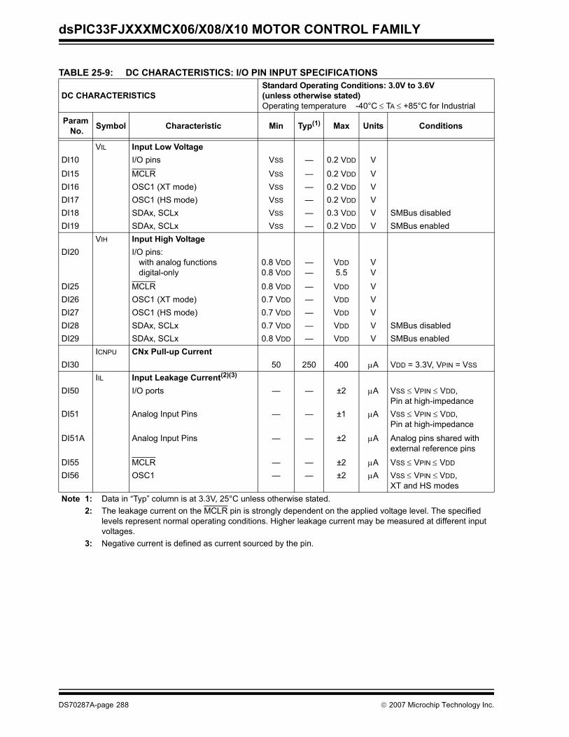
dsPIC33FJXXXMCX06/X08/X10 MOTOR CONTROL FAMILY
TABLE 25-9: DC CHARACTERISTICS: I/O PIN INPUT SPECIFICATIONS
DC CHARACTERISTICSStandard Operating Conditions: 3.0V to 3.6V(unless otherwise stated)Operating temperature -40°C ≤ TA ≤ +85°C for Industrial
Param No. Symbol Characteristic Min Typ(1) Max Units Conditions
VIL Input Low VoltageDI10 I/O pins VSS — 0.2 VDD V
DI15 MCLR VSS — 0.2 VDD VDI16 OSC1 (XT mode) VSS — 0.2 VDD VDI17 OSC1 (HS mode) VSS — 0.2 VDD VDI18 SDAx, SCLx VSS — 0.3 VDD V SMBus disabledDI19 SDAx, SCLx VSS — 0.2 VDD V SMBus enabled
VIH Input High VoltageDI20 I/O pins:
with analog functions digital-only
0.8 VDD0.8 VDD
——
VDD5.5
VV
DI25 MCLR 0.8 VDD — VDD VDI26 OSC1 (XT mode) 0.7 VDD — VDD VDI27 OSC1 (HS mode) 0.7 VDD — VDD VDI28 SDAx, SCLx 0.7 VDD — VDD V SMBus disabledDI29 SDAx, SCLx 0.8 VDD — VDD V SMBus enabled
ICNPU CNx Pull-up CurrentDI30 50 250 400 μA VDD = 3.3V, VPIN = VSS
IIL Input Leakage Current(2)(3)
DI50 I/O ports — — ±2 μA VSS ≤ VPIN ≤ VDD,Pin at high-impedance
DI51 Analog Input Pins — — ±1 μA VSS ≤ VPIN ≤ VDD,Pin at high-impedance
DI51A Analog Input Pins — — ±2 μA Analog pins shared with external reference pins
DI55 MCLR — — ±2 μA VSS ≤ VPIN ≤ VDD
DI56 OSC1 — — ±2 μA VSS ≤ VPIN ≤ VDD, XT and HS modes
Note 1: Data in “Typ” column is at 3.3V, 25°C unless otherwise stated.2: The leakage current on the MCLR pin is strongly dependent on the applied voltage level. The specified
levels represent normal operating conditions. Higher leakage current may be measured at different input voltages.
3: Negative current is defined as current sourced by the pin.
DS70287A-page 288 © 2007 Microchip Technology Inc.
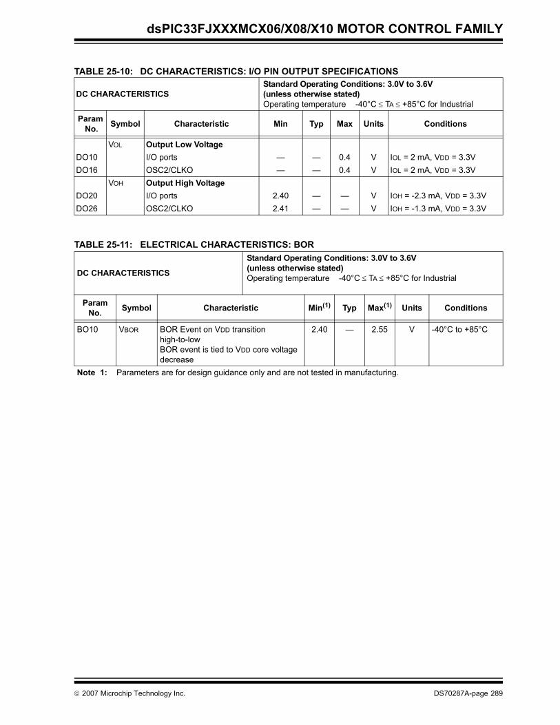
dsPIC33FJXXXMCX06/X08/X10 MOTOR CONTROL FAMILY
TABLE 25-10: DC CHARACTERISTICS: I/O PIN OUTPUT SPECIFICATIONS
DC CHARACTERISTICSStandard Operating Conditions: 3.0V to 3.6V(unless otherwise stated)Operating temperature -40°C ≤ TA ≤ +85°C for Industrial
Param No. Symbol Characteristic Min Typ Max Units Conditions
VOL Output Low VoltageDO10 I/O ports — — 0.4 V IOL = 2 mA, VDD = 3.3VDO16 OSC2/CLKO — — 0.4 V IOL = 2 mA, VDD = 3.3V
VOH Output High VoltageDO20 I/O ports 2.40 — — V IOH = -2.3 mA, VDD = 3.3VDO26 OSC2/CLKO 2.41 — — V IOH = -1.3 mA, VDD = 3.3V
TABLE 25-11: ELECTRICAL CHARACTERISTICS: BOR
DC CHARACTERISTICS
Standard Operating Conditions: 3.0V to 3.6V(unless otherwise stated)Operating temperature -40°C ≤ TA ≤ +85°C for Industrial
ParamNo. Symbol Characteristic Min(1) Typ Max(1) Units Conditions
BO10 VBOR BOR Event on VDD transition high-to-lowBOR event is tied to VDD core voltage decrease
2.40 — 2.55 V -40°C to +85°C
Note 1: Parameters are for design guidance only and are not tested in manufacturing.
© 2007 Microchip Technology Inc. DS70287A-page 289
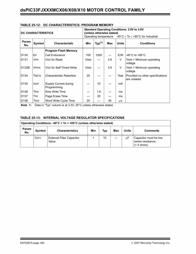
dsPIC33FJXXXMCX06/X08/X10 MOTOR CONTROL FAMILY
TABLE 25-13: INTERNAL VOLTAGE REGULATOR SPECIFICATIONS
TABLE 25-12: DC CHARACTERISTICS: PROGRAM MEMORY
DC CHARACTERISTICSStandard Operating Conditions: 3.0V to 3.6V(unless otherwise stated)Operating temperature -40°C ≤ TA ≤ +85°C for Industrial
ParamNo. Symbol Characteristic Min Typ(1) Max Units Conditions
Program Flash MemoryD130 EP Cell Endurance 100 1000 — E/W -40°C to +85°CD131 VPR VDD for Read VMIN — 3.6 V VMIN = Minimum operating
voltageD132B VPEW VDD for Self-Timed Write VMIN — 3.6 V VMIN = Minimum operating
voltageD134 TRETD Characteristic Retention 20 — — Year Provided no other specifications
are violatedD135 IDDP Supply Current during
Programming— 10 — mA
D136 TRW Row Write Time — 1.6 — msD137 TPE Page Erase Time — 20 — msD138 TWW Word Write Cycle Time 20 — 40 μsNote 1: Data in “Typ” column is at 3.3V, 25°C unless otherwise stated.
Operating Conditions: -40°C < TA < +85°C (unless otherwise stated)
ParamNo. Symbol Characteristics Min Typ Max Units Comments
CEFC External Filter Capacitor Value
1 10 — μF Capacitor must be low series resistance (< 5 ohms)
DS70287A-page 290 © 2007 Microchip Technology Inc.
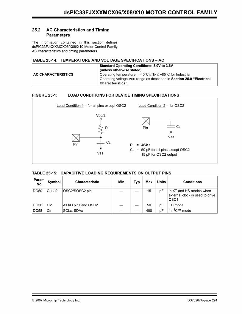
dsPIC33FJXXXMCX06/X08/X10 MOTOR CONTROL FAMILY
25.2 AC Characteristics and Timing Parameters
The information contained in this section definesdsPIC33FJXXXMCX06/X08/X10 Motor Control FamilyAC characteristics and timing parameters.
TABLE 25-14: TEMPERATURE AND VOLTAGE SPECIFICATIONS – AC
FIGURE 25-1: LOAD CONDITIONS FOR DEVICE TIMING SPECIFICATIONS
TABLE 25-15: CAPACITIVE LOADING REQUIREMENTS ON OUTPUT PINS
AC CHARACTERISTICS
Standard Operating Conditions: 3.0V to 3.6V(unless otherwise stated)Operating temperature -40°C ≤ TA ≤ +85°C for Industrial Operating voltage VDD range as described in Section 25.0 “Electrical Characteristics”.
Param No. Symbol Characteristic Min Typ Max Units Conditions
DO50 COSC2 OSC2/SOSC2 pin — — 15 pF In XT and HS modes when external clock is used to drive OSC1
DO56 CIO All I/O pins and OSC2 — — 50 pF EC mode DO58 CB SCLx, SDAx — — 400 pF In I2C™ mode
VDD/2
CL
RL
Pin
Pin
VSS
VSS
CL
RL = 464ΩCL = 50 pF for all pins except OSC2
15 pF for OSC2 output
Load Condition 1 – for all pins except OSC2 Load Condition 2 – for OSC2
© 2007 Microchip Technology Inc. DS70287A-page 291
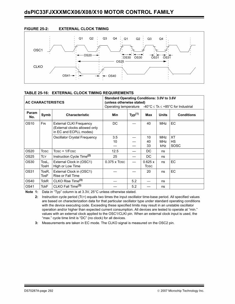
dsPIC33FJXXXMCX06/X08/X10 MOTOR CONTROL FAMILY
FIGURE 25-2: EXTERNAL CLOCK TIMING
Q1 Q2 Q3 Q4
OSC1
CLKO
Q1 Q2 Q3 Q4
OS20
OS25OS30 OS30
OS40OS41
OS31 OS31
TABLE 25-16: EXTERNAL CLOCK TIMING REQUIREMENTS
AC CHARACTERISTICSStandard Operating Conditions: 3.0V to 3.6V(unless otherwise stated)Operating temperature -40°C ≤ TA ≤ +85°C for Industrial
ParamNo. Symb Characteristic Min Typ(1) Max Units Conditions
OS10 FIN External CLKI Frequency(External clocks allowed onlyin EC and ECPLL modes)
DC — 40 MHz EC
Oscillator Crystal Frequency 3.510—
———
104033
MHzMHzkHz
XTHSSOSC
OS20 TOSC TOSC = 1/FOSC 12.5 — DC nsOS25 TCY Instruction Cycle Time(2) 25 — DC nsOS30 TosL,
TosHExternal Clock in (OSC1)High or Low Time
0.375 x TOSC — 0.625 x TOSC
ns EC
OS31 TosR,TosF
External Clock in (OSC1)Rise or Fall Time
— — 20 ns EC
OS40 TckR CLKO Rise Time(3) — 5.2 — nsOS41 TckF CLKO Fall Time(3) — 5.2 — nsNote 1: Data in “Typ” column is at 3.3V, 25°C unless otherwise stated.
2: Instruction cycle period (TCY) equals two times the input oscillator time-base period. All specified values are based on characterization data for that particular oscillator type under standard operating conditions with the device executing code. Exceeding these specified limits may result in an unstable oscillator operation and/or higher than expected current consumption. All devices are tested to operate at “min.” values with an external clock applied to the OSC1/CLKI pin. When an external clock input is used, the “max.” cycle time limit is “DC” (no clock) for all devices.
3: Measurements are taken in EC mode. The CLKO signal is measured on the OSC2 pin.
DS70287A-page 292 © 2007 Microchip Technology Inc.
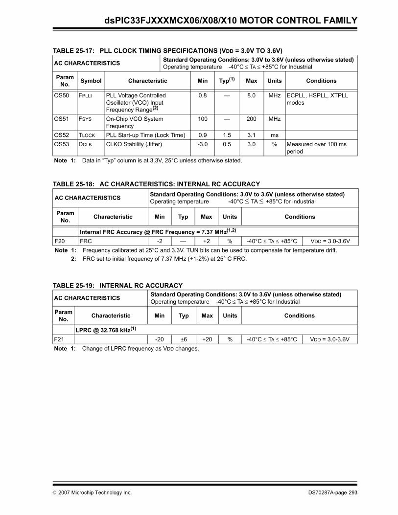
dsPIC33FJXXXMCX06/X08/X10 MOTOR CONTROL FAMILY
TABLE 25-17: PLL CLOCK TIMING SPECIFICATIONS (VDD = 3.0V TO 3.6V)
AC CHARACTERISTICS Standard Operating Conditions: 3.0V to 3.6V (unless otherwise stated)Operating temperature -40°C ≤ TA ≤ +85°C for Industrial
ParamNo. Symbol Characteristic Min Typ(1) Max Units Conditions
OS50 FPLLI PLL Voltage Controlled Oscillator (VCO) Input Frequency Range(2)
0.8 — 8.0 MHz ECPLL, HSPLL, XTPLL modes
OS51 FSYS On-Chip VCO System Frequency
100 — 200 MHz
OS52 TLOCK PLL Start-up Time (Lock Time) 0.9 1.5 3.1 msOS53 DCLK CLKO Stability (Jitter) -3.0 0.5 3.0 % Measured over 100 ms
periodNote 1: Data in “Typ” column is at 3.3V, 25°C unless otherwise stated.
TABLE 25-18: AC CHARACTERISTICS: INTERNAL RC ACCURACY
AC CHARACTERISTICS Standard Operating Conditions: 3.0V to 3.6V (unless otherwise stated)Operating temperature -40°C ≤ TA ≤ +85°C for industrial
Param No. Characteristic Min Typ Max Units Conditions
Internal FRC Accuracy @ FRC Frequency = 7.37 MHz(1,2)
F20 FRC -2 — +2 % -40°C ≤ TA ≤ +85°C VDD = 3.0-3.6VNote 1: Frequency calibrated at 25°C and 3.3V. TUN bits can be used to compensate for temperature drift.
2: FRC set to initial frequency of 7.37 MHz (+1-2%) at 25° C FRC.
TABLE 25-19: INTERNAL RC ACCURACY
AC CHARACTERISTICS Standard Operating Conditions: 3.0V to 3.6V (unless otherwise stated)Operating temperature -40°C ≤ TA ≤ +85°C for Industrial
ParamNo. Characteristic Min Typ Max Units Conditions
LPRC @ 32.768 kHz(1)
F21 -20 ±6 +20 % -40°C ≤ TA ≤ +85°C VDD = 3.0-3.6VNote 1: Change of LPRC frequency as VDD changes.
© 2007 Microchip Technology Inc. DS70287A-page 293
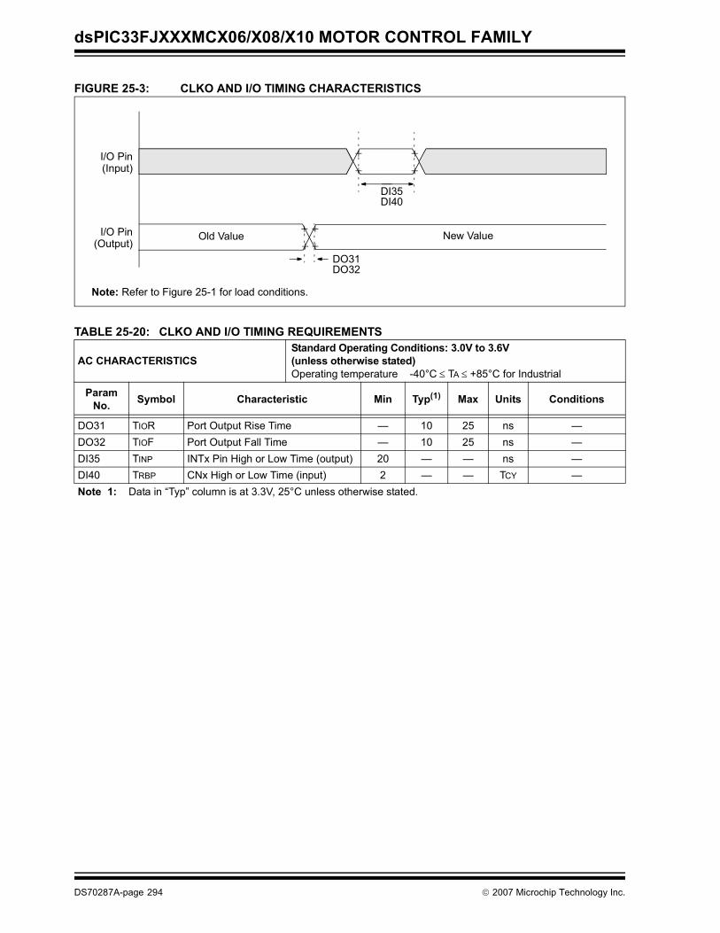
dsPIC33FJXXXMCX06/X08/X10 MOTOR CONTROL FAMILY
FIGURE 25-3: CLKO AND I/O TIMING CHARACTERISTICS
TABLE 25-20: CLKO AND I/O TIMING REQUIREMENTS
AC CHARACTERISTICSStandard Operating Conditions: 3.0V to 3.6V(unless otherwise stated)Operating temperature -40°C ≤ TA ≤ +85°C for Industrial
ParamNo. Symbol Characteristic Min Typ(1) Max Units Conditions
DO31 TIOR Port Output Rise Time — 10 25 ns —DO32 TIOF Port Output Fall Time — 10 25 ns —DI35 TINP INTx Pin High or Low Time (output) 20 — — ns —DI40 TRBP CNx High or Low Time (input) 2 — — TCY —Note 1: Data in “Typ” column is at 3.3V, 25°C unless otherwise stated.
Note: Refer to Figure 25-1 for load conditions.
I/O Pin(Input)
I/O Pin(Output)
DI35
Old Value New Value
DI40
DO31DO32
DS70287A-page 294 © 2007 Microchip Technology Inc.
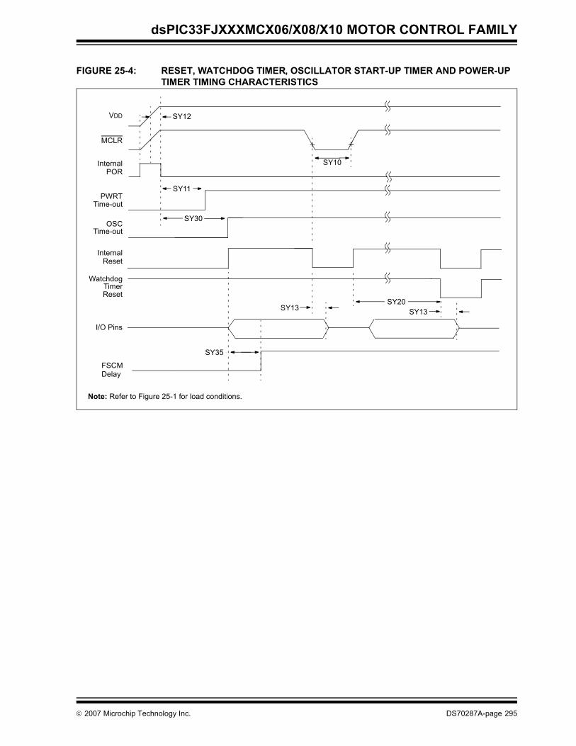
dsPIC33FJXXXMCX06/X08/X10 MOTOR CONTROL FAMILY
FIGURE 25-4: RESET, WATCHDOG TIMER, OSCILLATOR START-UP TIMER AND POWER-UP TIMER TIMING CHARACTERISTICS
VDD
MCLR
InternalPOR
PWRTTime-out
OSCTime-out
InternalReset
WatchdogTimerReset
SY11
SY10
SY20SY13
I/O Pins
SY13
Note: Refer to Figure 25-1 for load conditions.
FSCM Delay
SY35
SY30
SY12
© 2007 Microchip Technology Inc. DS70287A-page 295
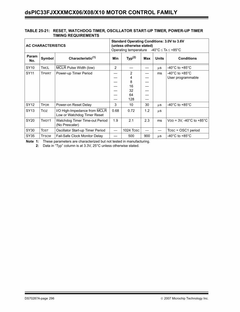
dsPIC33FJXXXMCX06/X08/X10 MOTOR CONTROL FAMILY
TABLE 25-21: RESET, WATCHDOG TIMER, OSCILLATOR START-UP TIMER, POWER-UP TIMER TIMING REQUIREMENTS
AC CHARACTERISTICSStandard Operating Conditions: 3.0V to 3.6V(unless otherwise stated)Operating temperature -40°C ≤ TA ≤ +85°C
ParamNo. Symbol Characteristic(1) Min Typ(2) Max Units Conditions
SY10 TMCL MCLR Pulse Width (low) 2 — — μs -40°C to +85°CSY11 TPWRT Power-up Timer Period —
——————
248
163264128
———————
ms -40°C to +85°CUser programmable
SY12 TPOR Power-on Reset Delay 3 10 30 μs -40°C to +85°C
SY13 TIOZ I/O High-Impedance from MCLR Low or Watchdog Timer Reset
0.68 0.72 1.2 μs
SY20 TWDT1 Watchdog Timer Time-out Period (No Prescaler)
1.9 2.1 2.3 ms VDD = 3V, -40°C to +85°C
SY30 TOST Oscillator Start-up Timer Period — 1024 TOSC — — TOSC = OSC1 periodSY35 TFSCM Fail-Safe Clock Monitor Delay — 500 900 μs -40°C to +85°CNote 1: These parameters are characterized but not tested in manufacturing.
2: Data in “Typ” column is at 3.3V, 25°C unless otherwise stated.
DS70287A-page 296 © 2007 Microchip Technology Inc.
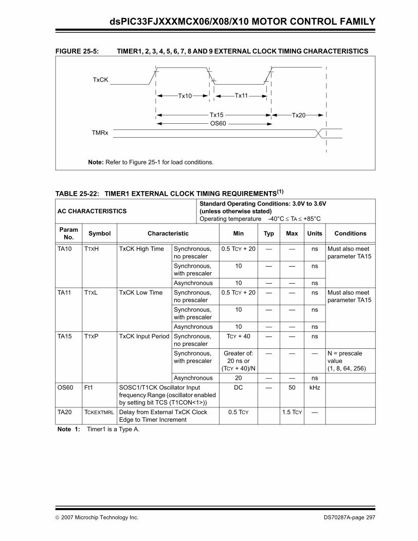
dsPIC33FJXXXMCX06/X08/X10 MOTOR CONTROL FAMILY
FIGURE 25-5: TIMER1, 2, 3, 4, 5, 6, 7, 8 AND 9 EXTERNAL CLOCK TIMING CHARACTERISTICS
Note: Refer to Figure 25-1 for load conditions.
Tx11
Tx15
Tx10
Tx20
TMRxOS60
TxCK
TABLE 25-22: TIMER1 EXTERNAL CLOCK TIMING REQUIREMENTS(1)
AC CHARACTERISTICSStandard Operating Conditions: 3.0V to 3.6V(unless otherwise stated)Operating temperature -40°C ≤ TA ≤ +85°C
ParamNo. Symbol Characteristic Min Typ Max Units Conditions
TA10 TTXH TxCK High Time Synchronous,no prescaler
0.5 TCY + 20 — — ns Must also meet parameter TA15
Synchronous,with prescaler
10 — — ns
Asynchronous 10 — — nsTA11 TTXL TxCK Low Time Synchronous,
no prescaler0.5 TCY + 20 — — ns Must also meet
parameter TA15Synchronous,with prescaler
10 — — ns
Asynchronous 10 — — nsTA15 TTXP TxCK Input Period Synchronous,
no prescalerTCY + 40 — — ns
Synchronous,with prescaler
Greater of:20 ns or
(TCY + 40)/N
— — — N = prescale value(1, 8, 64, 256)
Asynchronous 20 — — nsOS60 Ft1 SOSC1/T1CK Oscillator Input
frequency Range (oscillator enabled by setting bit TCS (T1CON<1>))
DC — 50 kHz
TA20 TCKEXTMRL Delay from External TxCK Clock Edge to Timer Increment
0.5 TCY 1.5 TCY —
Note 1: Timer1 is a Type A.
© 2007 Microchip Technology Inc. DS70287A-page 297
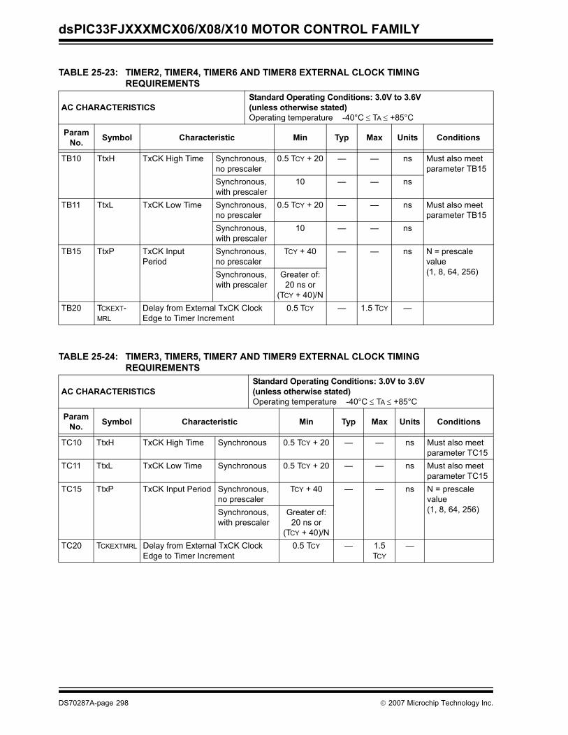
dsPIC33FJXXXMCX06/X08/X10 MOTOR CONTROL FAMILY
TABLE 25-23: TIMER2, TIMER4, TIMER6 AND TIMER8 EXTERNAL CLOCK TIMING REQUIREMENTS
AC CHARACTERISTICSStandard Operating Conditions: 3.0V to 3.6V(unless otherwise stated)Operating temperature -40°C ≤ TA ≤ +85°C
ParamNo. Symbol Characteristic Min Typ Max Units Conditions
TB10 TtxH TxCK High Time Synchronous,no prescaler
0.5 TCY + 20 — — ns Must also meet parameter TB15
Synchronous,with prescaler
10 — — ns
TB11 TtxL TxCK Low Time Synchronous,no prescaler
0.5 TCY + 20 — — ns Must also meet parameter TB15
Synchronous,with prescaler
10 — — ns
TB15 TtxP TxCK Input Period
Synchronous,no prescaler
TCY + 40 — — ns N = prescale value(1, 8, 64, 256)Synchronous,
with prescalerGreater of:
20 ns or(TCY + 40)/N
TB20 TCKEXT-MRL
Delay from External TxCK Clock Edge to Timer Increment
0.5 TCY — 1.5 TCY —
TABLE 25-24: TIMER3, TIMER5, TIMER7 AND TIMER9 EXTERNAL CLOCK TIMING REQUIREMENTS
AC CHARACTERISTICSStandard Operating Conditions: 3.0V to 3.6V(unless otherwise stated)Operating temperature -40°C ≤ TA ≤ +85°C
ParamNo. Symbol Characteristic Min Typ Max Units Conditions
TC10 TtxH TxCK High Time Synchronous 0.5 TCY + 20 — — ns Must also meet parameter TC15
TC11 TtxL TxCK Low Time Synchronous 0.5 TCY + 20 — — ns Must also meet parameter TC15
TC15 TtxP TxCK Input Period Synchronous,no prescaler
TCY + 40 — — ns N = prescalevalue (1, 8, 64, 256)Synchronous,
with prescalerGreater of:
20 ns or (TCY + 40)/N
TC20 TCKEXTMRL Delay from External TxCK Clock Edge to Timer Increment
0.5 TCY — 1.5 TCY
—
DS70287A-page 298 © 2007 Microchip Technology Inc.
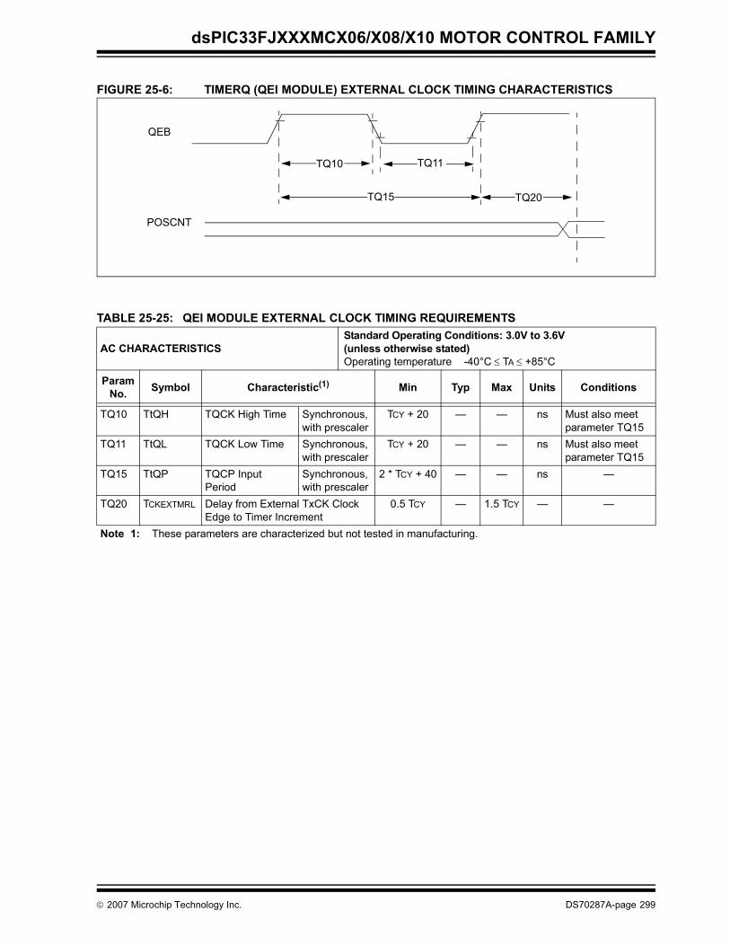
dsPIC33FJXXXMCX06/X08/X10 MOTOR CONTROL FAMILY
FIGURE 25-6: TIMERQ (QEI MODULE) EXTERNAL CLOCK TIMING CHARACTERISTICS
TQ11
TQ15
TQ10
TQ20
QEB
POSCNT
TABLE 25-25: QEI MODULE EXTERNAL CLOCK TIMING REQUIREMENTS
AC CHARACTERISTICSStandard Operating Conditions: 3.0V to 3.6V(unless otherwise stated)Operating temperature -40°C ≤ TA ≤ +85°C
ParamNo. Symbol Characteristic(1) Min Typ Max Units Conditions
TQ10 TtQH TQCK High Time Synchronous,with prescaler
TCY + 20 — — ns Must also meet parameter TQ15
TQ11 TtQL TQCK Low Time Synchronous,with prescaler
TCY + 20 — — ns Must also meet parameter TQ15
TQ15 TtQP TQCP Input Period
Synchronous,with prescaler
2 * TCY + 40 — — ns —
TQ20 TCKEXTMRL Delay from External TxCK Clock Edge to Timer Increment
0.5 TCY — 1.5 TCY — —
Note 1: These parameters are characterized but not tested in manufacturing.
© 2007 Microchip Technology Inc. DS70287A-page 299
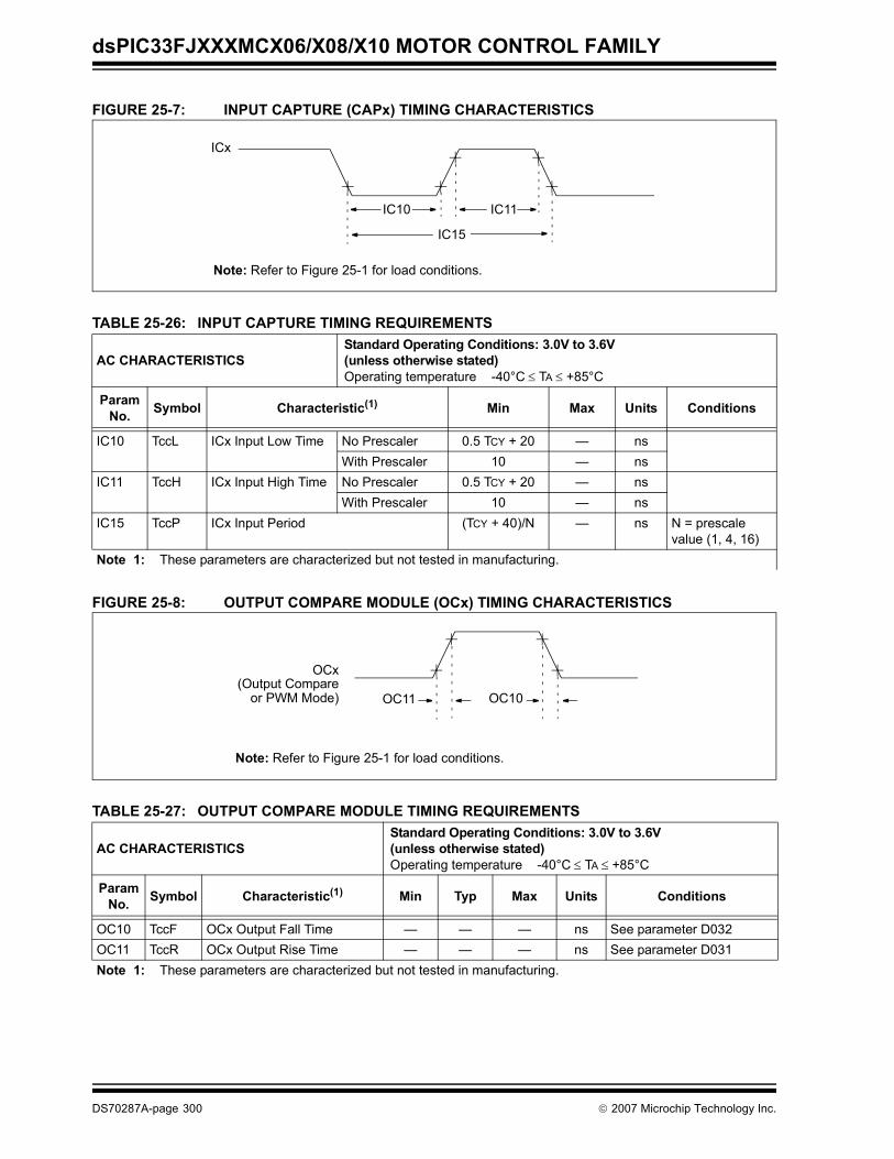
dsPIC33FJXXXMCX06/X08/X10 MOTOR CONTROL FAMILY
FIGURE 25-7: INPUT CAPTURE (CAPx) TIMING CHARACTERISTICS
FIGURE 25-8: OUTPUT COMPARE MODULE (OCx) TIMING CHARACTERISTICS
TABLE 25-26: INPUT CAPTURE TIMING REQUIREMENTS
AC CHARACTERISTICSStandard Operating Conditions: 3.0V to 3.6V(unless otherwise stated)Operating temperature -40°C ≤ TA ≤ +85°C
ParamNo. Symbol Characteristic(1) Min Max Units Conditions
IC10 TccL ICx Input Low Time No Prescaler 0.5 TCY + 20 — nsWith Prescaler 10 — ns
IC11 TccH ICx Input High Time No Prescaler 0.5 TCY + 20 — nsWith Prescaler 10 — ns
IC15 TccP ICx Input Period (TCY + 40)/N — ns N = prescale value (1, 4, 16)
Note 1: These parameters are characterized but not tested in manufacturing.
TABLE 25-27: OUTPUT COMPARE MODULE TIMING REQUIREMENTS
AC CHARACTERISTICSStandard Operating Conditions: 3.0V to 3.6V(unless otherwise stated)Operating temperature -40°C ≤ TA ≤ +85°C
Param No. Symbol Characteristic(1) Min Typ Max Units Conditions
OC10 TccF OCx Output Fall Time — — — ns See parameter D032OC11 TccR OCx Output Rise Time — — — ns See parameter D031Note 1: These parameters are characterized but not tested in manufacturing.
ICx
IC10 IC11
IC15
Note: Refer to Figure 25-1 for load conditions.
OCx
OC11 OC10(Output Compare
Note: Refer to Figure 25-1 for load conditions.
or PWM Mode)
DS70287A-page 300 © 2007 Microchip Technology Inc.
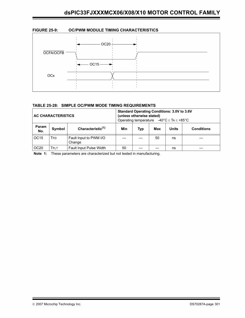
dsPIC33FJXXXMCX06/X08/X10 MOTOR CONTROL FAMILY
FIGURE 25-9: OC/PWM MODULE TIMING CHARACTERISTICS
OCFA/OCFB
OCx
OC20
OC15
TABLE 25-28: SIMPLE OC/PWM MODE TIMING REQUIREMENTS
AC CHARACTERISTICSStandard Operating Conditions: 3.0V to 3.6V(unless otherwise stated)Operating temperature -40°C ≤ TA ≤ +85°C
Param No. Symbol Characteristic(1) Min Typ Max Units Conditions
OC15 TFD Fault Input to PWM I/O Change
— — 50 ns —
OC20 TFLT Fault Input Pulse Width 50 — — ns —Note 1: These parameters are characterized but not tested in manufacturing.
© 2007 Microchip Technology Inc. DS70287A-page 301
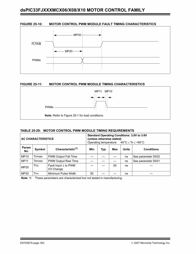
dsPIC33FJXXXMCX06/X08/X10 MOTOR CONTROL FAMILY
FIGURE 25-10: MOTOR CONTROL PWM MODULE FAULT TIMING CHARACTERISTICS
FIGURE 25-11: MOTOR CONTROL PWM MODULE TIMING CHARACTERISTICS
FLTA/B
PWMx
MP30
MP20
PWMx
MP11 MP10
Note: Refer to Figure 25-1 for load conditions.
TABLE 25-29: MOTOR CONTROL PWM MODULE TIMING REQUIREMENTS
AC CHARACTERISTICSStandard Operating Conditions: 3.0V to 3.6V(unless otherwise stated)Operating temperature -40°C ≤ TA ≤ +85°C
ParamNo. Symbol Characteristic(1) Min Typ Max Units Conditions
MP10 TFPWM PWM Output Fall Time — — — ns See parameter D032MP11 TRPWM PWM Output Rise Time — — — ns See parameter D031
MP20 TFD Fault Input ↓ to PWMI/O Change
— — 50 ns —
MP30 TFH Minimum Pulse Width 50 — — ns —Note 1: These parameters are characterized but not tested in manufacturing.
DS70287A-page 302 © 2007 Microchip Technology Inc.
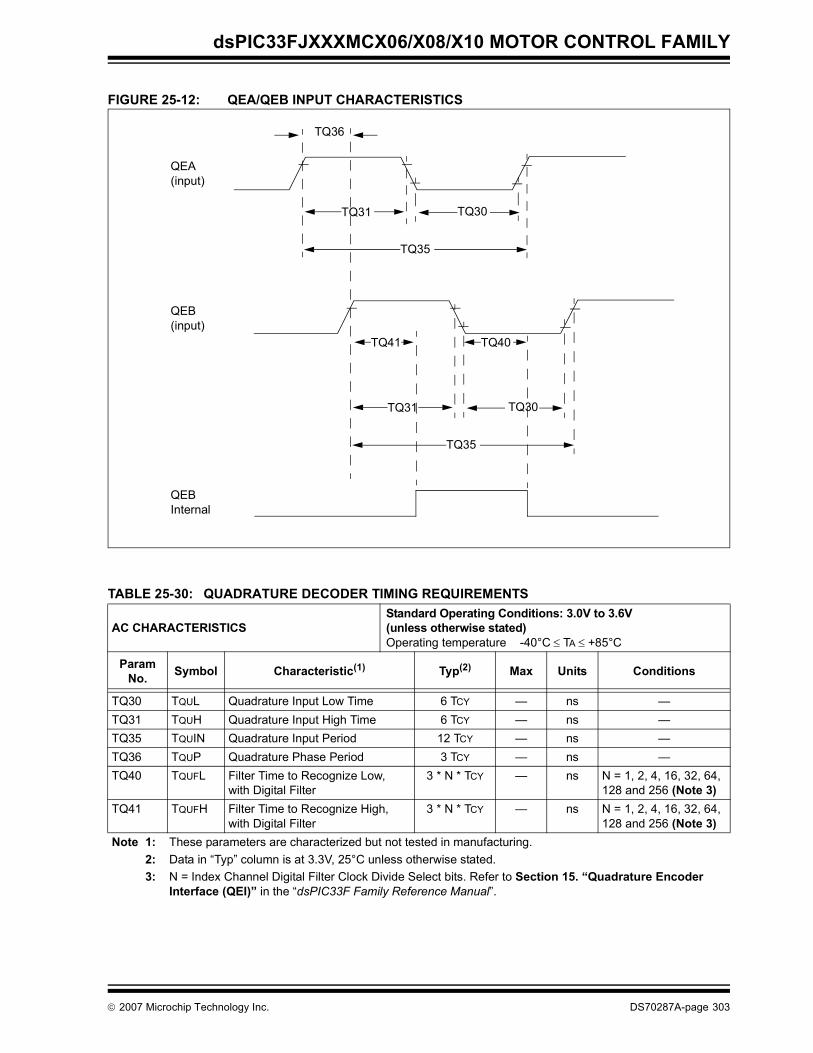
dsPIC33FJXXXMCX06/X08/X10 MOTOR CONTROL FAMILY
FIGURE 25-12: QEA/QEB INPUT CHARACTERISTICS
TQ30
TQ35
TQ31
QEA (input)
TQ30
TQ35
TQ31
QEB (input)
TQ36
QEB Internal
TQ40TQ41
TABLE 25-30: QUADRATURE DECODER TIMING REQUIREMENTS
AC CHARACTERISTICSStandard Operating Conditions: 3.0V to 3.6V(unless otherwise stated)Operating temperature -40°C ≤ TA ≤ +85°C
ParamNo. Symbol Characteristic(1) Typ(2) Max Units Conditions
TQ30 TQUL Quadrature Input Low Time 6 TCY — ns —TQ31 TQUH Quadrature Input High Time 6 TCY — ns —TQ35 TQUIN Quadrature Input Period 12 TCY — ns —TQ36 TQUP Quadrature Phase Period 3 TCY — ns —TQ40 TQUFL Filter Time to Recognize Low,
with Digital Filter3 * N * TCY — ns N = 1, 2, 4, 16, 32, 64,
128 and 256 (Note 3)TQ41 TQUFH Filter Time to Recognize High,
with Digital Filter3 * N * TCY — ns N = 1, 2, 4, 16, 32, 64,
128 and 256 (Note 3)Note 1: These parameters are characterized but not tested in manufacturing.
2: Data in “Typ” column is at 3.3V, 25°C unless otherwise stated.3: N = Index Channel Digital Filter Clock Divide Select bits. Refer to Section 15. “Quadrature Encoder
Interface (QEI)” in the “dsPIC33F Family Reference Manual”.
© 2007 Microchip Technology Inc. DS70287A-page 303
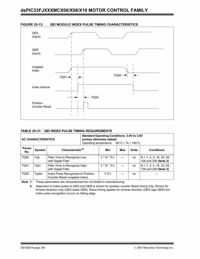
dsPIC33FJXXXMCX06/X08/X10 MOTOR CONTROL FAMILY
FIGURE 25-13: QEI MODULE INDEX PULSE TIMING CHARACTERISTICS
QEA(input)
UngatedIndex
QEB(input)
TQ55
Index Internal
PositionCounter Reset
TQ50TQ51
TABLE 25-31: QEI INDEX PULSE TIMING REQUIREMENTS
AC CHARACTERISTICSStandard Operating Conditions: 3.0V to 3.6V(unless otherwise stated)Operating temperature -40°C ≤ TA ≤ +85°C
ParamNo. Symbol Characteristic(1) Min Max Units Conditions
TQ50 TqIL Filter Time to Recognize Low,with Digital Filter
3 * N * TCY — ns N = 1, 2, 4, 16, 32, 64,128 and 256 (Note 2)
TQ51 TqiH Filter Time to Recognize High,with Digital Filter
3 * N * TCY — ns N = 1, 2, 4, 16, 32, 64,128 and 256 (Note 2)
TQ55 Tqidxr Index Pulse Recognized to PositionCounter Reset (ungated index)
3 TCY — ns —
Note 1: These parameters are characterized but not tested in manufacturing.2: Alignment of index pulses to QEA and QEB is shown for position counter Reset timing only. Shown for
forward direction only (QEA leads QEB). Same timing applies for reverse direction (QEA lags QEB) but index pulse recognition occurs on falling edge.
DS70287A-page 304 © 2007 Microchip Technology Inc.
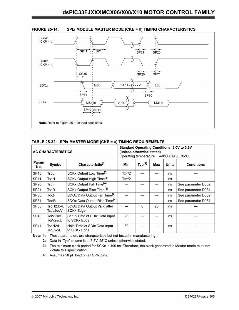
dsPIC33FJXXXMCX06/X08/X10 MOTOR CONTROL FAMILY
FIGURE 25-14: SPIx MODULE MASTER MODE (CKE = 0) TIMING CHARACTERISTICS
SCKx(CKP = 0)
SCKx(CKP = 1)
SDOx
SDIx
SP11 SP10
SP40 SP41
SP21SP20SP35
SP20SP21
MSb LSbBit 14 - - - - - -1
MSb In LSb InBit 14 - - - -1
SP30SP31
Note: Refer to Figure 25-1 for load conditions.
TABLE 25-32: SPIx MASTER MODE (CKE = 0) TIMING REQUIREMENTS
AC CHARACTERISTICSStandard Operating Conditions: 3.0V to 3.6V(unless otherwise stated)Operating temperature -40°C ≤ TA ≤ +85°C
ParamNo. Symbol Characteristic(1) Min Typ(2) Max Units Conditions
SP10 TscL SCKx Output Low Time(3) TCY/2 — — ns —SP11 TscH SCKx Output High Time(3) TCY/2 — — ns —SP20 TscF SCKx Output Fall Time(4) — — — ns See parameter D032SP21 TscR SCKx Output Rise Time(4) — — — ns See parameter D031SP30 TdoF SDOx Data Output Fall Time(4) — — — ns See parameter D032SP31 TdoR SDOx Data Output Rise Time(4) — — — ns See parameter D031SP35 TscH2doV,
TscL2doVSDOx Data Output Valid after SCKx Edge
— 6 20 ns —
SP40 TdiV2scH,TdiV2scL
Setup Time of SDIx Data Inputto SCKx Edge
23 — — ns —
SP41 TscH2diL,TscL2diL
Hold Time of SDIx Data Inputto SCKx Edge
30 — — ns —
Note 1: These parameters are characterized but not tested in manufacturing.2: Data in “Typ” column is at 3.3V, 25°C unless otherwise stated.3: The minimum clock period for SCKx is 100 ns. Therefore, the clock generated in Master mode must not
violate this specification.4: Assumes 50 pF load on all SPIx pins.
© 2007 Microchip Technology Inc. DS70287A-page 305
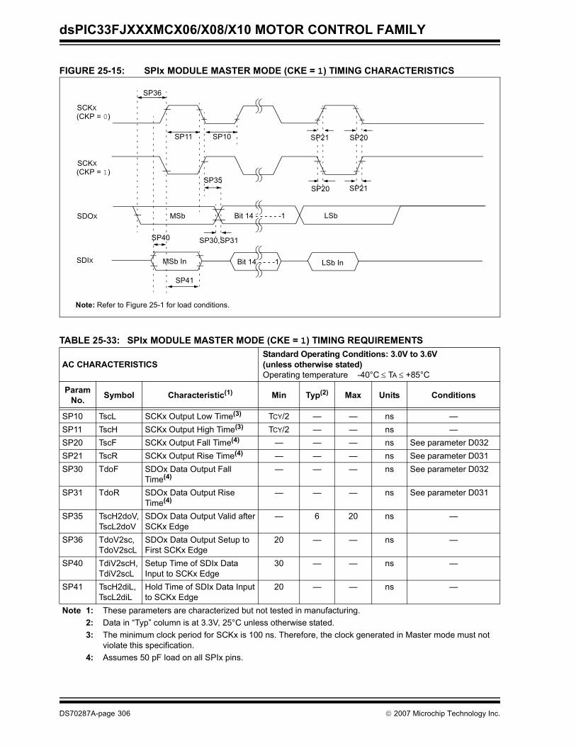
dsPIC33FJXXXMCX06/X08/X10 MOTOR CONTROL FAMILY
FIGURE 25-15: SPIx MODULE MASTER MODE (CKE = 1) TIMING CHARACTERISTICS
SCKX(CKP = 0)
SCKX(CKP = 1)
SDOX
SDIX
SP36
SP30,SP31
SP35
MSb
MSb In
Bit 14 - - - - - -1
LSb InBit 14 - - - -1
LSb
Note: Refer to Figure 25-1 for load conditions.
SP11 SP10 SP20SP21
SP21SP20
SP40
SP41
TABLE 25-33: SPIx MODULE MASTER MODE (CKE = 1) TIMING REQUIREMENTS
AC CHARACTERISTICSStandard Operating Conditions: 3.0V to 3.6V(unless otherwise stated)Operating temperature -40°C ≤ TA ≤ +85°C
ParamNo. Symbol Characteristic(1) Min Typ(2) Max Units Conditions
SP10 TscL SCKx Output Low Time(3) TCY/2 — — ns —SP11 TscH SCKx Output High Time(3) TCY/2 — — ns —SP20 TscF SCKx Output Fall Time(4) — — — ns See parameter D032SP21 TscR SCKx Output Rise Time(4) — — — ns See parameter D031SP30 TdoF SDOx Data Output Fall
Time(4)— — — ns See parameter D032
SP31 TdoR SDOx Data Output Rise Time(4)
— — — ns See parameter D031
SP35 TscH2doV,TscL2doV
SDOx Data Output Valid afterSCKx Edge
— 6 20 ns —
SP36 TdoV2sc, TdoV2scL
SDOx Data Output Setup toFirst SCKx Edge
20 — — ns —
SP40 TdiV2scH, TdiV2scL
Setup Time of SDIx Data Input to SCKx Edge
30 — — ns —
SP41 TscH2diL, TscL2diL
Hold Time of SDIx Data Inputto SCKx Edge
20 — — ns —
Note 1: These parameters are characterized but not tested in manufacturing.2: Data in “Typ” column is at 3.3V, 25°C unless otherwise stated.3: The minimum clock period for SCKx is 100 ns. Therefore, the clock generated in Master mode must not
violate this specification.4: Assumes 50 pF load on all SPIx pins.
DS70287A-page 306 © 2007 Microchip Technology Inc.
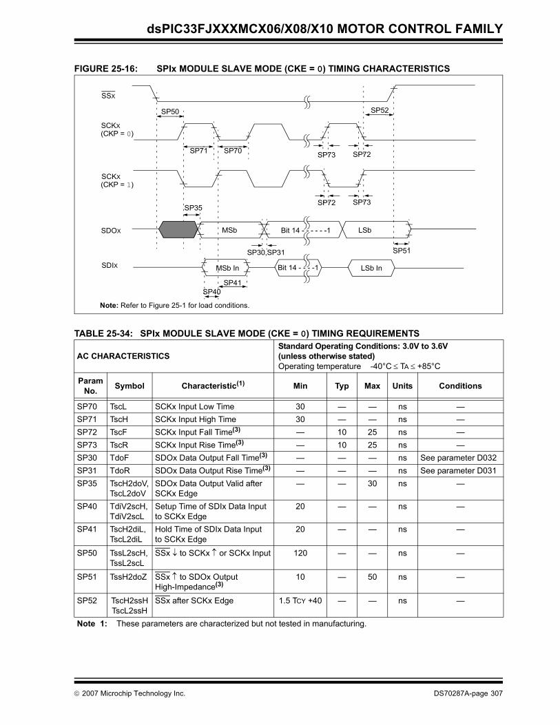
dsPIC33FJXXXMCX06/X08/X10 MOTOR CONTROL FAMILY
FIGURE 25-16: SPIx MODULE SLAVE MODE (CKE = 0) TIMING CHARACTERISTICS
TABLE 25-34: SPIx MODULE SLAVE MODE (CKE = 0) TIMING REQUIREMENTS
AC CHARACTERISTICSStandard Operating Conditions: 3.0V to 3.6V(unless otherwise stated)Operating temperature -40°C ≤ TA ≤ +85°C
ParamNo. Symbol Characteristic(1) Min Typ Max Units Conditions
SP70 TscL SCKx Input Low Time 30 — — ns —SP71 TscH SCKx Input High Time 30 — — ns —SP72 TscF SCKx Input Fall Time(3) — 10 25 ns —SP73 TscR SCKx Input Rise Time(3) — 10 25 ns —SP30 TdoF SDOx Data Output Fall Time(3) — — — ns See parameter D032SP31 TdoR SDOx Data Output Rise Time(3) — — — ns See parameter D031SP35 TscH2doV,
TscL2doVSDOx Data Output Valid afterSCKx Edge
— — 30 ns —
SP40 TdiV2scH, TdiV2scL
Setup Time of SDIx Data Inputto SCKx Edge
20 — — ns —
SP41 TscH2diL, TscL2diL
Hold Time of SDIx Data Inputto SCKx Edge
20 — — ns —
SP50 TssL2scH, TssL2scL
SSx ↓ to SCKx ↑ or SCKx Input 120 — — ns —
SP51 TssH2doZ SSx ↑ to SDOx OutputHigh-Impedance(3)
10 — 50 ns —
SP52 TscH2ssHTscL2ssH
SSx after SCKx Edge 1.5 TCY +40 — — ns —
Note 1: These parameters are characterized but not tested in manufacturing.
SSX
SCKX(CKP = 0)
SCKX(CKP = 1)
SDOX
SP50
SP40SP41
SP30,SP31 SP51
SP35
MSb LSbBit 14 - - - - - -1
MSb In Bit 14 - - - -1 LSb In
SP52
SP73SP72
SP72SP73SP71 SP70
Note: Refer to Figure 25-1 for load conditions.
SDIX
© 2007 Microchip Technology Inc. DS70287A-page 307
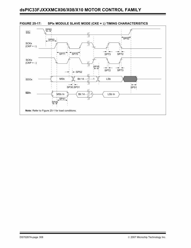
dsPIC33FJXXXMCX06/X08/X10 MOTOR CONTROL FAMILY
FIGURE 25-17: SPIx MODULE SLAVE MODE (CKE = 1) TIMING CHARACTERISTICS
SSx
SCKx(CKP = 0)
SCKx(CKP = 1)
SDOx
SDI
SP50
SP60
SDIx
SP30,SP31
MSb Bit 14 - - - - - -1 LSb
SP51
MSb In Bit 14 - - - -1 LSb In
SP35
SP52
SP52
SP73SP72
SP72SP73SP71 SP70
SP40SP41
Note: Refer to Figure 25-1 for load conditions.
DS70287A-page 308 © 2007 Microchip Technology Inc.
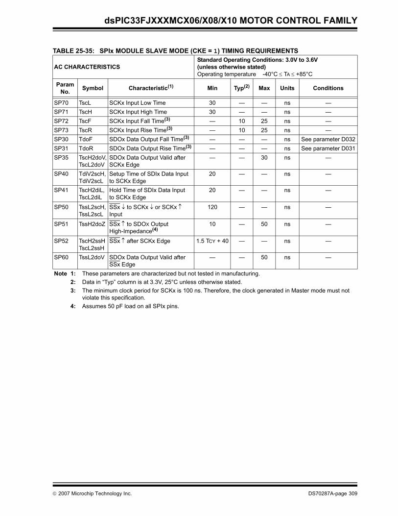
dsPIC33FJXXXMCX06/X08/X10 MOTOR CONTROL FAMILY
TABLE 25-35: SPIx MODULE SLAVE MODE (CKE = 1) TIMING REQUIREMENTS
AC CHARACTERISTICSStandard Operating Conditions: 3.0V to 3.6V(unless otherwise stated)Operating temperature -40°C ≤ TA ≤ +85°C
ParamNo. Symbol Characteristic(1) Min Typ(2) Max Units Conditions
SP70 TscL SCKx Input Low Time 30 — — ns —SP71 TscH SCKx Input High Time 30 — — ns —SP72 TscF SCKx Input Fall Time(3) — 10 25 ns —SP73 TscR SCKx Input Rise Time(3) — 10 25 ns —SP30 TdoF SDOx Data Output Fall Time(3) — — — ns See parameter D032SP31 TdoR SDOx Data Output Rise Time(3) — — — ns See parameter D031SP35 TscH2doV,
TscL2doVSDOx Data Output Valid afterSCKx Edge
— — 30 ns —
SP40 TdiV2scH, TdiV2scL
Setup Time of SDIx Data Inputto SCKx Edge
20 — — ns —
SP41 TscH2diL, TscL2diL
Hold Time of SDIx Data Inputto SCKx Edge
20 — — ns —
SP50 TssL2scH, TssL2scL
SSx ↓ to SCKx ↓ or SCKx ↑ Input
120 — — ns —
SP51 TssH2doZ SSx ↑ to SDOX OutputHigh-Impedance(4)
10 — 50 ns —
SP52 TscH2ssHTscL2ssH
SSx ↑ after SCKx Edge 1.5 TCY + 40 — — ns —
SP60 TssL2doV SDOx Data Output Valid afterSSx Edge
— — 50 ns —
Note 1: These parameters are characterized but not tested in manufacturing.2: Data in “Typ” column is at 3.3V, 25°C unless otherwise stated.3: The minimum clock period for SCKx is 100 ns. Therefore, the clock generated in Master mode must not
violate this specification.4: Assumes 50 pF load on all SPIx pins.
© 2007 Microchip Technology Inc. DS70287A-page 309

dsPIC33FJXXXMCX06/X08/X10 MOTOR CONTROL FAMILY
FIGURE 25-18: I2Cx BUS START/STOP BITS TIMING CHARACTERISTICS (MASTER MODE)
FIGURE 25-19: I2Cx BUS DATA TIMING CHARACTERISTICS (MASTER MODE)
IM31 IM34SCLx
SDAx
StartCondition
StopCondition
IM30 IM33
Note: Refer to Figure 25-1 for load conditions.
IM11IM10 IM33
IM11IM10
IM20
IM26IM25
IM40 IM40 IM45
IM21
SCLx
SDAxIn
SDAxOut
Note: Refer to Figure 25-1 for load conditions.
DS70287A-page 310 © 2007 Microchip Technology Inc.
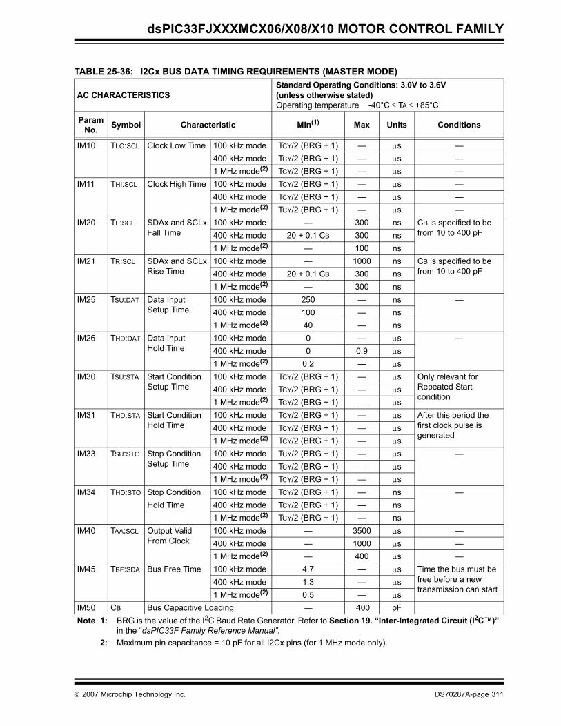
dsPIC33FJXXXMCX06/X08/X10 MOTOR CONTROL FAMILY
TABLE 25-36: I2Cx BUS DATA TIMING REQUIREMENTS (MASTER MODE)
AC CHARACTERISTICSStandard Operating Conditions: 3.0V to 3.6V(unless otherwise stated)Operating temperature -40°C ≤ TA ≤ +85°C
ParamNo. Symbol Characteristic Min(1) Max Units Conditions
IM10 TLO:SCL Clock Low Time 100 kHz mode TCY/2 (BRG + 1) — μs —400 kHz mode TCY/2 (BRG + 1) — μs —1 MHz mode(2) TCY/2 (BRG + 1) — μs —
IM11 THI:SCL Clock High Time 100 kHz mode TCY/2 (BRG + 1) — μs —400 kHz mode TCY/2 (BRG + 1) — μs —1 MHz mode(2) TCY/2 (BRG + 1) — μs —
IM20 TF:SCL SDAx and SCLxFall Time
100 kHz mode — 300 ns CB is specified to be from 10 to 400 pF400 kHz mode 20 + 0.1 CB 300 ns
1 MHz mode(2) — 100 nsIM21 TR:SCL SDAx and SCLx
Rise Time100 kHz mode — 1000 ns CB is specified to be
from 10 to 400 pF400 kHz mode 20 + 0.1 CB 300 ns1 MHz mode(2) — 300 ns
IM25 TSU:DAT Data InputSetup Time
100 kHz mode 250 — ns —400 kHz mode 100 — ns1 MHz mode(2) 40 — ns
IM26 THD:DAT Data InputHold Time
100 kHz mode 0 — μs —400 kHz mode 0 0.9 μs1 MHz mode(2) 0.2 — μs
IM30 TSU:STA Start ConditionSetup Time
100 kHz mode TCY/2 (BRG + 1) — μs Only relevant for Repeated Startcondition
400 kHz mode TCY/2 (BRG + 1) — μs1 MHz mode(2) TCY/2 (BRG + 1) — μs
IM31 THD:STA Start Condition Hold Time
100 kHz mode TCY/2 (BRG + 1) — μs After this period thefirst clock pulse isgenerated
400 kHz mode TCY/2 (BRG + 1) — μs1 MHz mode(2) TCY/2 (BRG + 1) — μs
IM33 TSU:STO Stop Condition Setup Time
100 kHz mode TCY/2 (BRG + 1) — μs —400 kHz mode TCY/2 (BRG + 1) — μs1 MHz mode(2) TCY/2 (BRG + 1) — μs
IM34 THD:STO Stop Condition 100 kHz mode TCY/2 (BRG + 1) — ns —Hold Time 400 kHz mode TCY/2 (BRG + 1) — ns
1 MHz mode(2) TCY/2 (BRG + 1) — nsIM40 TAA:SCL Output Valid
From Clock100 kHz mode — 3500 μs —400 kHz mode — 1000 μs —1 MHz mode(2) — 400 μs —
IM45 TBF:SDA Bus Free Time 100 kHz mode 4.7 — μs Time the bus must be free before a newtransmission can start
400 kHz mode 1.3 — μs1 MHz mode(2) 0.5 — μs
IM50 CB Bus Capacitive Loading — 400 pF Note 1: BRG is the value of the I2C Baud Rate Generator. Refer to Section 19. “Inter-Integrated Circuit (I2C™)”
in the “dsPIC33F Family Reference Manual”.2: Maximum pin capacitance = 10 pF for all I2Cx pins (for 1 MHz mode only).
© 2007 Microchip Technology Inc. DS70287A-page 311
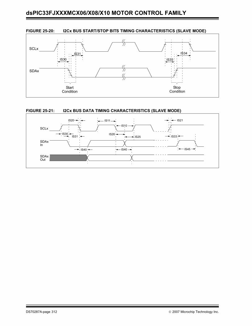
dsPIC33FJXXXMCX06/X08/X10 MOTOR CONTROL FAMILY
FIGURE 25-20: I2Cx BUS START/STOP BITS TIMING CHARACTERISTICS (SLAVE MODE)
FIGURE 25-21: I2Cx BUS DATA TIMING CHARACTERISTICS (SLAVE MODE)
IS31 IS34SCLx
SDAx
StartCondition
StopCondition
IS30 IS33
IS30IS31 IS33
IS11
IS10
IS20
IS26IS25
IS40 IS40 IS45
IS21
SCLx
SDAxIn
SDAxOut
DS70287A-page 312 © 2007 Microchip Technology Inc.
dsPIC33FJXXXMCX06/X08/X10 MOTOR CONTROL FAMILY
TABLE 25-37: I2Cx BUS DATA TIMING REQUIREMENTS (SLAVE MODE)
AC CHARACTERISTICSStandard Operating Conditions: 3.0V to 3.6V(unless otherwise stated)Operating temperature -40°C ≤ TA ≤ +85°C
ParamNo. Symbol Characteristic Min Max Units Conditions
IS10 TLO:SCL Clock Low Time 100 kHz mode 4.7 — μs Device must operate at a minimum of 1.5 MHz
400 kHz mode 1.3 — μs Device must operate at a minimum of 10 MHz
1 MHz mode(1) 0.5 — μs —IS11 THI:SCL Clock High Time 100 kHz mode 4.0 — μs Device must operate at a
minimum of 1.5 MHz400 kHz mode 0.6 — μs Device must operate at a
minimum of 10 MHz1 MHz mode(1) 0.5 — μs —
IS20 TF:SCL SDAx and SCLxFall Time
100 kHz mode — 300 ns CB is specified to be from10 to 400 pF400 kHz mode 20 + 0.1 CB 300 ns
1 MHz mode(1) — 100 nsIS21 TR:SCL SDAx and SCLx
Rise Time100 kHz mode — 1000 ns CB is specified to be from
10 to 400 pF400 kHz mode 20 + 0.1 CB 300 ns1 MHz mode(1) — 300 ns
IS25 TSU:DAT Data InputSetup Time
100 kHz mode 250 — ns —400 kHz mode 100 — ns1 MHz mode(1) 100 — ns
IS26 THD:DAT Data InputHold Time
100 kHz mode 0 — μs —400 kHz mode 0 0.9 μs1 MHz mode(1) 0 0.3 μs
IS30 TSU:STA Start ConditionSetup Time
100 kHz mode 4.7 — μs Only relevant for Repeated Start condition400 kHz mode 0.6 — μs
1 MHz mode(1) 0.25 — μsIS31 THD:STA Start Condition
Hold Time 100 kHz mode 4.0 — μs After this period, the first
clock pulse is generated400 kHz mode 0.6 — μs1 MHz mode(1) 0.25 — μs
IS33 TSU:STO Stop Condition Setup Time
100 kHz mode 4.7 — μs —400 kHz mode 0.6 — μs1 MHz mode(1) 0.6 — μs
IS34 THD:STO Stop ConditionHold Time
100 kHz mode 4000 — ns —400 kHz mode 600 — ns1 MHz mode(1) 250 ns
IS40 TAA:SCL Output Valid From Clock
100 kHz mode 0 3500 ns —400 kHz mode 0 1000 ns1 MHz mode(1) 0 350 ns
IS45 TBF:SDA Bus Free Time 100 kHz mode 4.7 — μs Time the bus must be free before a new transmission can start
400 kHz mode 1.3 — μs1 MHz mode(1) 0.5 — μs
IS50 CB Bus Capacitive Loading — 400 pF —Note 1: Maximum pin capacitance = 10 pF for all I2Cx pins (for 1 MHz mode only).
© 2007 Microchip Technology Inc. DS70287A-page 313
dsPIC33FJXXXMCX06/X08/X10 MOTOR CONTROL FAMILY
FIGURE 25-22: CAN MODULE I/O TIMING CHARACTERISTICS
CiTx Pin(output)
CA10 CA11
Old Value New Value
CA20
CiRx Pin(input)
TABLE 25-38: CAN MODULE I/O TIMING REQUIREMENTS
AC CHARACTERISTICSStandard Operating Conditions: 3.0V to 3.6V(unless otherwise stated)Operating temperature -40°C ≤ TA ≤ +85°C
ParamNo. Symbol Characteristic(1) Min Typ Max Units Conditions
CA10 TioF Port Output Fall Time — — — ns See parameter D032CA11 TioR Port Output Rise Time — — — ns See parameter D031CA20 Tcwf Pulse Width to Trigger
CAN Wake-up Filter120 — — ns —
Note 1: These parameters are characterized but not tested in manufacturing.
DS70287A-page 314 © 2007 Microchip Technology Inc.
dsPIC33FJXXXMCX06/X08/X10 MOTOR CONTROL FAMILY
TABLE 25-39: ADC MODULE SPECIFICATIONS
AC CHARACTERISTICSStandard Operating Conditions: 3.0V to 3.6V(unless otherwise stated)Operating temperature -40°C ≤ TA ≤ +85°C for Industrial
Param No. Symbol Characteristic Min. Typ Max. Units Conditions
Device SupplyAD01 AVDD Module VDD Supply Greater of
VDD – 0.3or 3.0
— Lesser ofVDD + 0.3
or 3.6
V—
AD02 AVSS Module VSS Supply VSS – 0.3 — VSS + 0.3 V —Reference Inputs
AD05 VREFH Reference Voltage High AVSS + 2.7 — AVDD V See Note 1AD05a 3.0 — 3.6 V VREFH = AVDD
VREFL = AVSS = 0AD06 VREFL Reference Voltage Low AVSS — AVDD – 2.7 V See Note 1AD06a 0 — 0 V VREFH = AVDD
VREFL = AVSS = 0AD07 VREF Absolute Reference Voltage 2.7 — 3.6 V VREF = VREFH - VREFL
AD08 IREF Current Drain — 400—
55010
μAμA
ADC operatingADC off
Analog InputAD12 VINH Input Voltage Range VINH VINL — VREFH V This voltage reflects
Sample and Hold Channels 0, 1, 2, and 3 (CH0-CH3), positive input
AD13 VINL Input Voltage Range VINL VREFL — AVSS + 1V V This voltage reflects Sample and Hold Channels 0, 1, 2, and 3 (CH0-CH3), negative input
AD17 RIN Recommended Impedance of Analog Voltage Source
——
——
200200
ΩΩ
10-bit ADC12-bit ADC
Note 1: These parameters are not characterized or tested in manufacturing.
© 2007 Microchip Technology Inc. DS70287A-page 315
dsPIC33FJXXXMCX06/X08/X10 MOTOR CONTROL FAMILY
TABLE 25-40: ADC MODULE SPECIFICATIONS (12-BIT MODE)
AC CHARACTERISTICSStandard Operating Conditions: 3.0V to 3.6V(unless otherwise stated)Operating temperature -40°C ≤ TA ≤ +85°C for Industrial
Param No. Symbol Characteristic Min. Typ Max. Units Conditions
ADC Accuracy (12-bit Mode) – Measurements with external VREF+/VREF-AD20a Nr Resolution 12 data bits bitsAD21a INL Integral Nonlinearity -2 — +2 LSb VINL = AVSS = VREFL = 0V, AVDD
= VREFH = 3.6VAD22a DNL Differential Nonlinearity >-1 — <1 LSb VINL = AVSS = VREFL = 0V, AVDD
= VREFH = 3.6VAD23a GERR Gain Error 1.25 1.5 3 LSb VINL = AVSS = VREFL = 0V, AVDD
= VREFH = 3.6VAD24a EOFF Offset Error 1.25 1.52 2 LSb VINL = AVSS = VREFL = 0V, AVDD
= VREFH = 3.6VAD25a — Monotonicity — — — — Guaranteed
ADC Accuracy (12-bit Mode) – Measurements with internal VREF+/VREF-AD20b Nr Resolution 12 data bits bitsAD21b INL Integral Nonlinearity -2 — +2 LSb VINL = AVSS = 0V, AVDD = 3.6VAD22b DNL Differential Nonlinearity >-1 — <1 LSb VINL = AVSS = 0V, AVDD = 3.6VAD23b GERR Gain Error 2 3 7 LSb VINL = AVSS = 0V, AVDD = 3.6VAD24b EOFF Offset Error 2 3 5 LSb VINL = AVSS = 0V, AVDD = 3.6VAD25b — Monotonicity — — — — Guaranteed
Dynamic Performance (12-bit Mode)AD30a THD Total Harmonic Distortion -77 -69 -61 dB —AD31a SINAD Signal to Noise and
Distortion 59 63 64 dB —
AD32a SFDR Spurious Free DynamicRange
63 72 74 dB —
AD33a FNYQ Input Signal Bandwidth — — 250 kHz —AD34a ENOB Effective Number of Bits 10.95 11.1 — bits —
DS70287A-page 316 © 2007 Microchip Technology Inc.
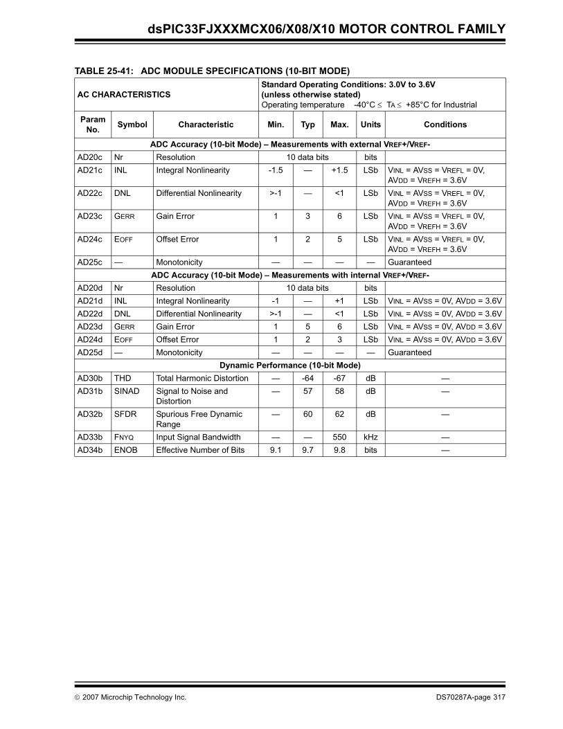
dsPIC33FJXXXMCX06/X08/X10 MOTOR CONTROL FAMILY
TABLE 25-41: ADC MODULE SPECIFICATIONS (10-BIT MODE)
AC CHARACTERISTICSStandard Operating Conditions: 3.0V to 3.6V(unless otherwise stated)Operating temperature -40°C ≤ TA ≤ +85°C for Industrial
Param No. Symbol Characteristic Min. Typ Max. Units Conditions
ADC Accuracy (10-bit Mode) – Measurements with external VREF+/VREF-AD20c Nr Resolution 10 data bits bitsAD21c INL Integral Nonlinearity -1.5 — +1.5 LSb VINL = AVSS = VREFL = 0V,
AVDD = VREFH = 3.6VAD22c DNL Differential Nonlinearity >-1 — <1 LSb VINL = AVSS = VREFL = 0V,
AVDD = VREFH = 3.6VAD23c GERR Gain Error 1 3 6 LSb VINL = AVSS = VREFL = 0V,
AVDD = VREFH = 3.6VAD24c EOFF Offset Error 1 2 5 LSb VINL = AVSS = VREFL = 0V,
AVDD = VREFH = 3.6VAD25c — Monotonicity — — — — Guaranteed
ADC Accuracy (10-bit Mode) – Measurements with internal VREF+/VREF-AD20d Nr Resolution 10 data bits bitsAD21d INL Integral Nonlinearity -1 — +1 LSb VINL = AVSS = 0V, AVDD = 3.6VAD22d DNL Differential Nonlinearity >-1 — <1 LSb VINL = AVSS = 0V, AVDD = 3.6VAD23d GERR Gain Error 1 5 6 LSb VINL = AVSS = 0V, AVDD = 3.6VAD24d EOFF Offset Error 1 2 3 LSb VINL = AVSS = 0V, AVDD = 3.6VAD25d — Monotonicity — — — — Guaranteed
Dynamic Performance (10-bit Mode)AD30b THD Total Harmonic Distortion — -64 -67 dB —AD31b SINAD Signal to Noise and
Distortion — 57 58 dB —
AD32b SFDR Spurious Free DynamicRange
— 60 62 dB —
AD33b FNYQ Input Signal Bandwidth — — 550 kHz —AD34b ENOB Effective Number of Bits 9.1 9.7 9.8 bits —
© 2007 Microchip Technology Inc. DS70287A-page 317
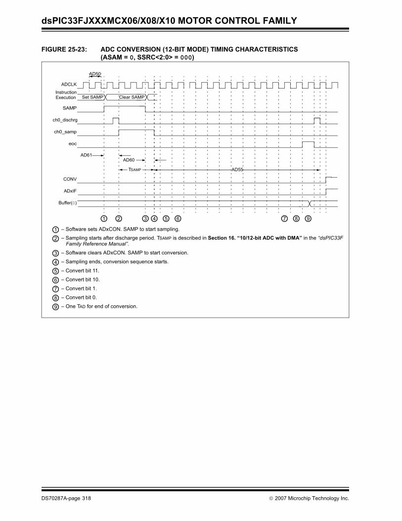
dsPIC33FJXXXMCX06/X08/X10 MOTOR CONTROL FAMILY
FIGURE 25-23: ADC CONVERSION (12-BIT MODE) TIMING CHARACTERISTICS (ASAM = 0, SSRC<2:0> = 000)
AD55TSAMP
Clear SAMPSet SAMP
AD61
ADCLK
Instruction
SAMP
ch0_dischrg
ch0_samp
AD60
CONV
ADxIF
Buffer(0)
1 2 3 4 5 6 87
1 – Software sets ADxCON. SAMP to start sampling.
2 – Sampling starts after discharge period. TSAMP is described in Section 16. “10/12-bit ADC with DMA” in the “dsPIC33F
3 – Software clears ADxCON. SAMP to start conversion.
4 – Sampling ends, conversion sequence starts.
5 – Convert bit 11.
9 – One TAD for end of conversion.
AD50
eoc
9
6 – Convert bit 10.
7 – Convert bit 1.
8 – Convert bit 0.
Execution
Family Reference Manual”.
DS70287A-page 318 © 2007 Microchip Technology Inc.
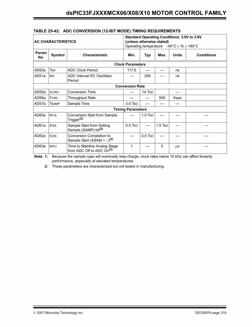
dsPIC33FJXXXMCX06/X08/X10 MOTOR CONTROL FAMILY
TABLE 25-42: ADC CONVERSION (12-BIT MODE) TIMING REQUIREMENTS
AC CHARACTERISTICSStandard Operating Conditions: 3.0V to 3.6V(unless otherwise stated)Operating temperature -40°C ≤ TA ≤ +85°C
Param No. Symbol Characteristic Min. Typ Max. Units Conditions
Clock ParametersAD50a TAD ADC Clock Period 117.6 — — nsAD51a tRC ADC Internal RC Oscillator
Period— 250 — ns
Conversion RateAD55a tCONV Conversion Time — 14 TAD —AD56a FCNV Throughput Rate — — 500 KspsAD57a TSAMP Sample Time 3.0 TAD — — —
Timing ParametersAD60a tPCS Conversion Start from Sample
Trigger(2)— 1.0 TAD — — —
AD61a tPSS Sample Start from SettingSample (SAMP) bit(2)
0.5 TAD — 1.5 TAD — —
AD62a tCSS Conversion Completion toSample Start (ASAM = 1)(2)
— 0.5 TAD — — —
AD63a tDPU Time to Stabilize Analog Stagefrom ADC Off to ADC On(2)
1 — 5 μs —
Note 1: Because the sample caps will eventually lose charge, clock rates below 10 kHz can affect linearity performance, especially at elevated temperatures.
2: These parameters are characterized but not tested in manufacturing.
© 2007 Microchip Technology Inc. DS70287A-page 319
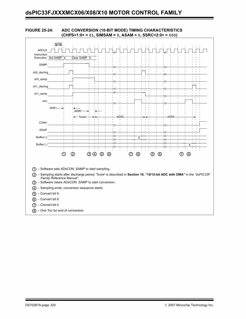
dsPIC33FJXXXMCX06/X08/X10 MOTOR CONTROL FAMILY
FIGURE 25-24: ADC CONVERSION (10-BIT MODE) TIMING CHARACTERISTICS(CHPS<1:0> = 01, SIMSAM = 0, ASAM = 0, SSRC<2:0> = 000)
AD55TSAMP
Clear SAMPSet SAMP
AD61
ADCLKInstruction
SAMP
ch0_dischrg
ch1_samp
AD60
CONV
ADxIF
Buffer(0)
Buffer(1)
1 2 3 4 5 6 8 5 6 7
1 – Software sets ADxCON. SAMP to start sampling.
2 – Sampling starts after discharge period. TSAMP is described in Section 16. “10/12-bit ADC with DMA” in the “dsPIC33F
3 – Software clears ADxCON. SAMP to start conversion.
4 – Sampling ends, conversion sequence starts.
5 – Convert bit 9.
8 – One TAD for end of conversion.
AD50
ch0_samp
ch1_dischrg
eoc
7
AD55
8
6 – Convert bit 8.
7 – Convert bit 0.
Execution
Family Reference Manual”.
DS70287A-page 320 © 2007 Microchip Technology Inc.
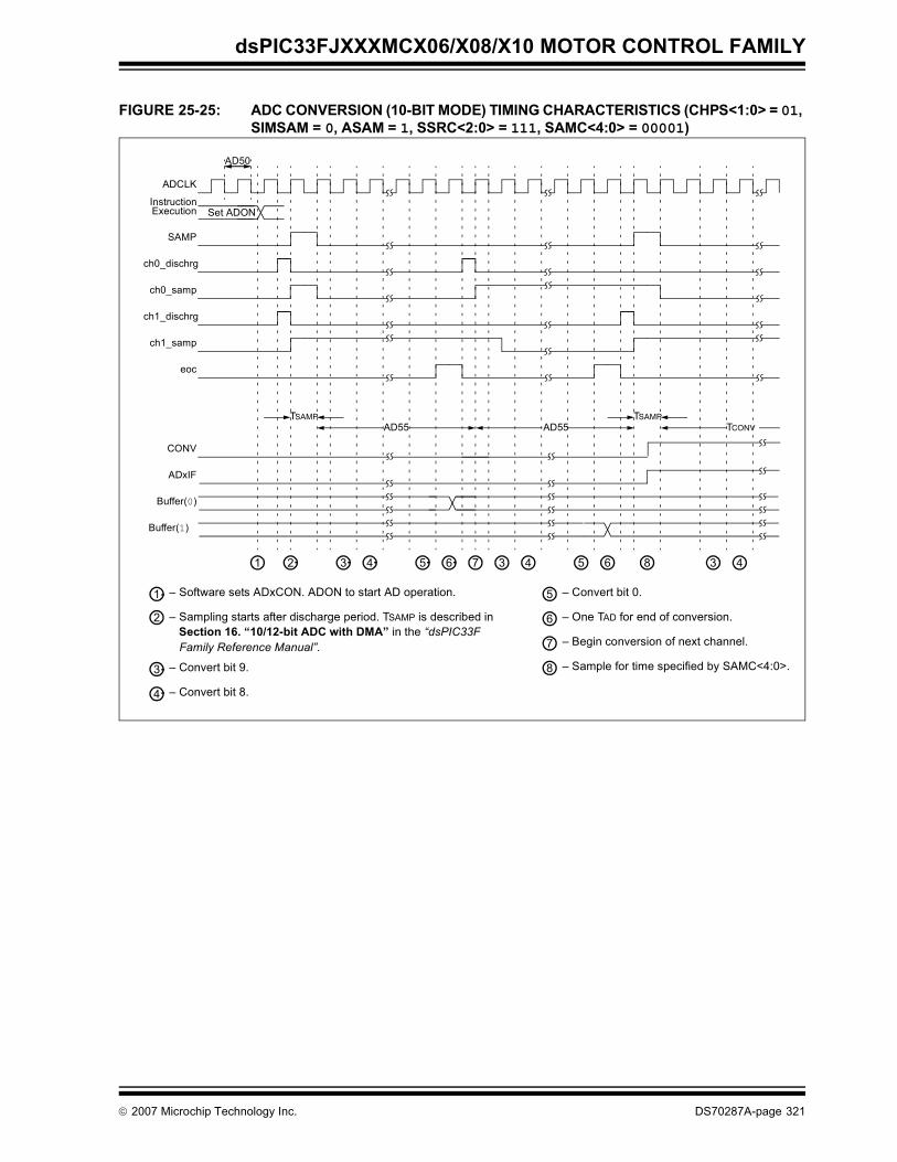
dsPIC33FJXXXMCX06/X08/X10 MOTOR CONTROL FAMILY
FIGURE 25-25: ADC CONVERSION (10-BIT MODE) TIMING CHARACTERISTICS (CHPS<1:0> = 01, SIMSAM = 0, ASAM = 1, SSRC<2:0> = 111, SAMC<4:0> = 00001)
AD55TSAMP
Set ADON
ADCLK
Instruction
SAMP
ch0_dischrg
ch1_samp
CONV
ADxIF
Buffer(0)
Buffer(1)
1 2 3 4 5 6 4 5 6 8
1 – Software sets ADxCON. ADON to start AD operation.
2 – Sampling starts after discharge period. TSAMP is described in
3 – Convert bit 9.
4 – Convert bit 8.
5 – Convert bit 0.
AD50
ch0_samp
ch1_dischrg
eoc
7 3
AD55
6 – One TAD for end of conversion.
7 – Begin conversion of next channel.
8 – Sample for time specified by SAMC<4:0>.
TSAMPTCONV
3 4
Execution
Section 16. “10/12-bit ADC with DMA” in the “dsPIC33F Family Reference Manual”.
© 2007 Microchip Technology Inc. DS70287A-page 321
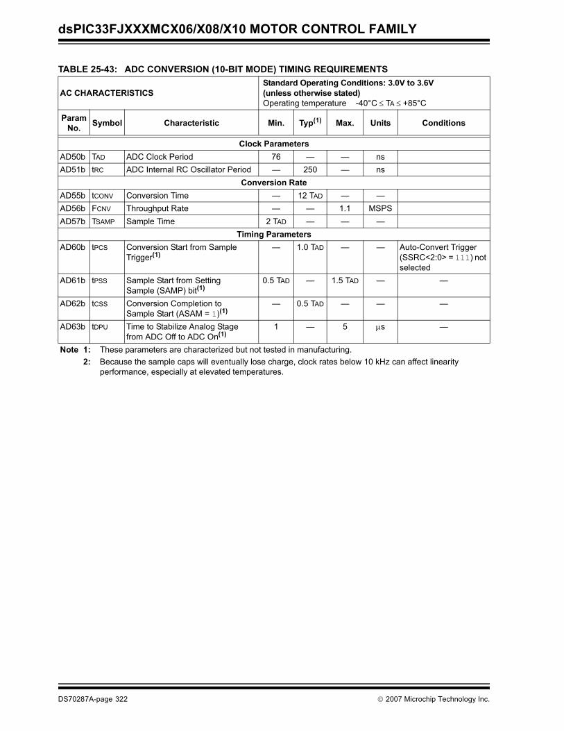
dsPIC33FJXXXMCX06/X08/X10 MOTOR CONTROL FAMILY
TABLE 25-43: ADC CONVERSION (10-BIT MODE) TIMING REQUIREMENTS
AC CHARACTERISTICSStandard Operating Conditions: 3.0V to 3.6V(unless otherwise stated)Operating temperature -40°C ≤ TA ≤ +85°C
Param No. Symbol Characteristic Min. Typ(1) Max. Units Conditions
Clock ParametersAD50b TAD ADC Clock Period 76 — — nsAD51b tRC ADC Internal RC Oscillator Period — 250 — ns
Conversion RateAD55b tCONV Conversion Time — 12 TAD — —AD56b FCNV Throughput Rate — — 1.1 MSPSAD57b TSAMP Sample Time 2 TAD — — —
Timing ParametersAD60b tPCS Conversion Start from Sample
Trigger(1)— 1.0 TAD — — Auto-Convert Trigger
(SSRC<2:0> = 111) not selected
AD61b tPSS Sample Start from SettingSample (SAMP) bit(1)
0.5 TAD — 1.5 TAD — —
AD62b tCSS Conversion Completion toSample Start (ASAM = 1)(1)
— 0.5 TAD — — —
AD63b tDPU Time to Stabilize Analog Stage from ADC Off to ADC On(1)
1 — 5 μs —
Note 1: These parameters are characterized but not tested in manufacturing.2: Because the sample caps will eventually lose charge, clock rates below 10 kHz can affect linearity
performance, especially at elevated temperatures.
DS70287A-page 322 © 2007 Microchip Technology Inc.
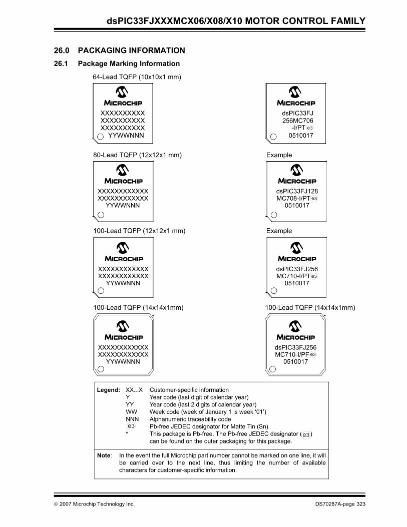
dsPIC33FJXXXMCX06/X08/X10 MOTOR CONTROL FAMILY
26.0 PACKAGING INFORMATION26.1 Package Marking Information
64-Lead TQFP (10x10x1 mm)
XXXXXXXXXXXXXXXXXXXXXXXXXXXXXX
YYWWNNN
80-Lead TQFP (12x12x1 mm)
XXXXXXXXXXXXXXXXXXXXXXXX
YYWWNNN
Legend: XX...X Customer-specific informationY Year code (last digit of calendar year)YY Year code (last 2 digits of calendar year)WW Week code (week of January 1 is week ‘01’)NNN Alphanumeric traceability code Pb-free JEDEC designator for Matte Tin (Sn)* This package is Pb-free. The Pb-free JEDEC designator ( )
can be found on the outer packaging for this package.
Note: In the event the full Microchip part number cannot be marked on one line, it willbe carried over to the next line, thus limiting the number of availablecharacters for customer-specific information.
3e
3e
100-Lead TQFP (12x12x1 mm)
XXXXXXXXXXXXXXXXXXXXXXXX
YYWWNNN
100-Lead TQFP (14x14x1mm)
XXXXXXXXXXXXXXXXXXXXXXXX
YYWWNNN
dsPIC33FJ256MC706
0510017
Example
dsPIC33FJ128
0510017
Example
dsPIC33FJ256MC710-I/PT
0510017
MC708-I/PT
100-Lead TQFP (14x14x1mm)
dsPIC33FJ256MC710-I/PF
0510017
-I/PT 3e
3e
3e
3e
© 2007 Microchip Technology Inc. DS70287A-page 323
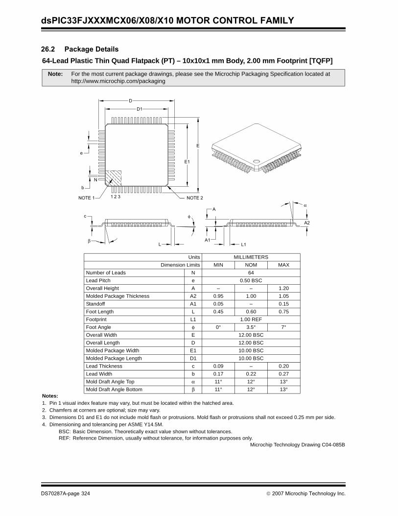
dsPIC33FJXXXMCX06/X08/X10 MOTOR CONTROL FAMILY
26.2 Package Details 64-Lead Plastic Thin Quad Flatpack (PT) – 10x10x1 mm Body, 2.00 mm Footprint [TQFP]
Notes:1. Pin 1 visual index feature may vary, but must be located within the hatched area.2. Chamfers at corners are optional; size may vary.3. Dimensions D1 and E1 do not include mold flash or protrusions. Mold flash or protrusions shall not exceed 0.25 mm per side.4. Dimensioning and tolerancing per ASME Y14.5M.
BSC: Basic Dimension. Theoretically exact value shown without tolerances.REF: Reference Dimension, usually without tolerance, for information purposes only.
Note: For the most current package drawings, please see the Microchip Packaging Specification located at http://www.microchip.com/packaging
Units MILLIMETERS
Dimension Limits MIN NOM MAX
Number of Leads N 64
Lead Pitch e 0.50 BSC
Overall Height A – – 1.20
Molded Package Thickness A2 0.95 1.00 1.05
Standoff A1 0.05 – 0.15
Foot Length L 0.45 0.60 0.75
Footprint L1 1.00 REF
Foot Angle φ 0° 3.5° 7°
Overall Width E 12.00 BSC
Overall Length D 12.00 BSC
Molded Package Width E1 10.00 BSC
Molded Package Length D1 10.00 BSC
Lead Thickness c 0.09 – 0.20
Lead Width b 0.17 0.22 0.27
Mold Draft Angle Top α 11° 12° 13°
Mold Draft Angle Bottom β 11° 12° 13°
D
D1
E
E1
e
b
N
NOTE 1 1 2 3 NOTE 2
c
L
A1
L1
A2
A
φ
β
α
Microchip Technology Drawing C04-085B
DS70287A-page 324 © 2007 Microchip Technology Inc.

dsPIC33FJXXXMCX06/X08/X10 MOTOR CONTROL FAMILY
80-Lead Plastic Thin Quad Flatpack (PT) – 12x12x1 mm Body, 2.00 mm Footprint [TQFP]
Notes:1. Pin 1 visual index feature may vary, but must be located within the hatched area.2. Chamfers at corners are optional; size may vary.3. Dimensions D1 and E1 do not include mold flash or protrusions. Mold flash or protrusions shall not exceed 0.25 mm per side.4. Dimensioning and tolerancing per ASME Y14.5M.
BSC: Basic Dimension. Theoretically exact value shown without tolerances.REF: Reference Dimension, usually without tolerance, for information purposes only.
Note: For the most current package drawings, please see the Microchip Packaging Specification located at http://www.microchip.com/packaging
Units MILLIMETERS
Dimension Limits MIN NOM MAX
Number of Leads N 80
Lead Pitch e 0.50 BSC
Overall Height A – – 1.20
Molded Package Thickness A2 0.95 1.00 1.05
Standoff A1 0.05 – 0.15
Foot Length L 0.45 0.60 0.75
Footprint L1 1.00 REF
Foot Angle φ 0° 3.5° 7°
Overall Width E 14.00 BSC
Overall Length D 14.00 BSC
Molded Package Width E1 12.00 BSC
Molded Package Length D1 12.00 BSC
Lead Thickness c 0.09 – 0.20
Lead Width b 0.17 0.22 0.27
Mold Draft Angle Top α 11° 12° 13°
Mold Draft Angle Bottom β 11° 12° 13°
D
D1
E
E1
e
bN
NOTE 112 3
NOTE 2
A
A2
L1
A1
L
c
α
βφ
Microchip Technology Drawing C04-092B
© 2007 Microchip Technology Inc. DS70287A-page 325
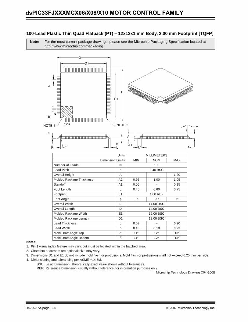
dsPIC33FJXXXMCX06/X08/X10 MOTOR CONTROL FAMILY
100-Lead Plastic Thin Quad Flatpack (PT) – 12x12x1 mm Body, 2.00 mm Footprint [TQFP]
Notes:1. Pin 1 visual index feature may vary, but must be located within the hatched area.2. Chamfers at corners are optional; size may vary.3. Dimensions D1 and E1 do not include mold flash or protrusions. Mold flash or protrusions shall not exceed 0.25 mm per side.4. Dimensioning and tolerancing per ASME Y14.5M.
BSC: Basic Dimension. Theoretically exact value shown without tolerances.REF: Reference Dimension, usually without tolerance, for information purposes only.
Note: For the most current package drawings, please see the Microchip Packaging Specification located at http://www.microchip.com/packaging
Units MILLIMETERS
Dimension Limits MIN NOM MAX
Number of Leads N 100
Lead Pitch e 0.40 BSC
Overall Height A – – 1.20
Molded Package Thickness A2 0.95 1.00 1.05
Standoff A1 0.05 – 0.15
Foot Length L 0.45 0.60 0.75
Footprint L1 1.00 REF
Foot Angle φ 0° 3.5° 7°
Overall Width E 14.00 BSC
Overall Length D 14.00 BSC
Molded Package Width E1 12.00 BSC
Molded Package Length D1 12.00 BSC
Lead Thickness c 0.09 – 0.20
Lead Width b 0.13 0.18 0.23
Mold Draft Angle Top α 11° 12° 13°
Mold Draft Angle Bottom β 11° 12° 13°
D
D1
E
E1
e
bN
123NOTE 1 NOTE 2
c
LA1
L1
A
A2
α
βφ
Microchip Technology Drawing C04-100B
DS70287A-page 326 © 2007 Microchip Technology Inc.
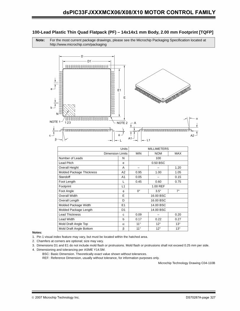
dsPIC33FJXXXMCX06/X08/X10 MOTOR CONTROL FAMILY
100-Lead Plastic Thin Quad Flatpack (PF) – 14x14x1 mm Body, 2.00 mm Footprint [TQFP]
Notes:1. Pin 1 visual index feature may vary, but must be located within the hatched area.2. Chamfers at corners are optional; size may vary.3. Dimensions D1 and E1 do not include mold flash or protrusions. Mold flash or protrusions shall not exceed 0.25 mm per side.4. Dimensioning and tolerancing per ASME Y14.5M.
BSC: Basic Dimension. Theoretically exact value shown without tolerances.REF: Reference Dimension, usually without tolerance, for information purposes only.
Note: For the most current package drawings, please see the Microchip Packaging Specification located at http://www.microchip.com/packaging
Units MILLIMETERS
Dimension Limits MIN NOM MAX
Number of Leads N 100
Lead Pitch e 0.50 BSC
Overall Height A – – 1.20
Molded Package Thickness A2 0.95 1.00 1.05
Standoff A1 0.05 – 0.15
Foot Length L 0.45 0.60 0.75
Footprint L1 1.00 REF
Foot Angle φ 0° 3.5° 7°
Overall Width E 16.00 BSC
Overall Length D 16.00 BSC
Molded Package Width E1 14.00 BSC
Molded Package Length D1 14.00 BSC
Lead Thickness c 0.09 – 0.20
Lead Width b 0.17 0.22 0.27
Mold Draft Angle Top α 11° 12° 13°
Mold Draft Angle Bottom β 11° 12° 13°
D
D1
e
b
E1
E
N
NOTE 1NOTE 21 23
c
LA1
L1
A2
A
φβ
α
Microchip Technology Drawing C04-110B
© 2007 Microchip Technology Inc. DS70287A-page 327

dsPIC33FJXXXMCX06/X08/X10 MOTOR CONTROL FAMILY
NOTES:
DS70287A-page 328 © 2007 Microchip Technology Inc.
dsPIC33FJXXXMCX06/X08/X10 Motor Control Family
APPENDIX A: DIFFERENCES BETWEEN “PS” (PROTOTYPE SAMPLE) DEVICES AND FINAL PRODUCTION DEVICES
The dsPIC33FJXXXMCX06/X08/X10 Motor ControlFamily devices marked “PS” have some key differ-ences from the final production devices (devices notmarked “PS”). The major differences are listed in thisappendix. In addition, there are minor differences inseveral SFR names, bits and Reset states, which aredescribed in Section 3.0 “Memory Organization”and the corresponding peripheral sections.
A.1 Device NamesThe Prototype Sample devices have a suffix “PS” intheir names, as marked on the device package. Thisdistinguishes them from Engineering Sample devices(which are suffixed “ES”) and final production devices(that have neither a “PS” nor an “ES” suffix on thedevice package marking).
Prototype samples are available only for a subset of thefinal production devices. Please refer to the devicetables in this data sheet for a listing of all devices.
A.2 RAM SizesThe total RAM size, including the size of the dual portedDMA RAM, is different between each “PS” device andthe corresponding final production device. For exam-ple, the final production devices have 2 Kbytes DMARAM, whereas the “PS” devices have 1 Kbyte DMARAM. Please refer to the device tables in this datasheet for the memory sizes of eachdsPIC33FJXXXMCX06/X08/X10 Motor Control Familydevice.
A.3 InterruptsThe final production devices have four more interruptsources (vectors) than the “PS” devices do. Also, twoof the interrupt vectors are associated with slightly dif-ferent events from the corresponding interrupts in the“PS” devices. Please refer to Section 6.0 “InterruptController” for more details.
A.4 DMA EnhancementsBoth “PS” and final production devices can performDirect Memory Access (DMA) data transfers.
In addition to all of the features supported by the DMAcontroller in the “PS” devices, the DMA controller in thefinal production devices also supports the PeripheralIndirect Addressing mode. Please refer to Section 7.0“Direct Memory Access (DMA)” for a description ofthis feature.
A.5 Oscillator OperationThe default values of the PLL postscaler and feedbackdivisor bits are different between the “PS” devices andfinal production devices. Please refer to Section 8.0“Oscillator Configuration” for the register definitionsand Reset states.
A.6 CAN and Enhanced CANThe dsPIC33FJXXXMCX06/X08/X10 Motor ControlFamily devices marked “PS” have up to two CAN mod-ules. The functionality and register layout of these mod-ules are identical to those of dsPIC30F devices, andare described in Section 20.0 “Enhanced CAN Mod-ule” of this data sheet. These modules do not provideDMA support.
The final production devices have up to two EnhancedCAN (ECAN™ technology) modules. These moduleshave significantly more features than the CAN mod-ules, mainly in the form of an increased number ofavailable buffers, filters and masks, as well as DMAsupport.
A.7 ADC DifferencesBoth “PS” and final production devices contain up totwo ADC modules.
The “PS” devices have a 16-word deep ADC resultbuffer.
The final production devices have enhanced DMA sup-port in the form of additional DMA RAM and PeripheralIndirect Addressing. This renders the 16-word ADCbuffer redundant. Hence, the buffer has been replacedby a single ADC Result register.
A.8 Device PackagesThe final production devices are offered in the followingTQFP packages:
• 64-pin TQFP 10x10x1 mm • 80-pin TQFP 12x12x1 mm • 100-pin TQFP 12x12x1 mm • 100-pin TQFP 14x14x1 mm
The “PS” devices are offered in the following TQFPpackages:
• 64-pin TQFP 10x10x1 mm • 80-pin TQFP 12x12x1 mm • 100-pin TQFP 14x14x1 mm
© 2007 Microchip Technology Inc. DS70287A-page 329
dsPIC33FJXXXMCX06/X08/X10 Motor Control Family
APPENDIX B: REVISION HISTORYRevision A (June 2007)Initial release of this document
DS70287A-page 330 © 2007 Microchip Technology Inc.
dsPIC33FJXXXMCX06/X08/X10 MOTOR CONTROL FAMILY
INDEXAA/D Converter ................................................................... 249
DMA .......................................................................... 249Initialization ............................................................... 249Key Features............................................................. 249
AC Characteristics ............................................................ 291Internal RC Accuracy ................................................ 293Load Conditions ........................................................ 291
ADC ModuleADC11 Register Map .................................................. 46ADC2 Register Map .................................................... 46
Alternate Vector Table (AIVT)............................................. 79Arithmetic Logic Unit (ALU)................................................. 23Assembler
MPASM Assembler................................................... 280Automatic Clock Stretch.................................................... 203
Receive Mode ........................................................... 203Transmit Mode .......................................................... 203
BBarrel Shifter ....................................................................... 27Bit-Reversed Addressing .................................................... 60
Example ...................................................................... 61Implementation ........................................................... 60Sequence Table (16-Entry)......................................... 61
Block Diagrams16-bit Timer1 Module ................................................ 149A/D Module ....................................................... 250, 251Connections for On-Chip Voltage Regulator............. 267Device Clock ..................................................... 137, 139DSP Engine ................................................................ 24dsPIC33F .................................................................... 14dsPIC33F CPU Core................................................... 18ECAN Module ........................................................... 220Input Capture ............................................................ 157Output Compare ....................................................... 161PLL............................................................................ 139PWM Module ............................................................ 164Quadrature Encoder Interface .................................. 185Reset System.............................................................. 73Shared Port Structure ............................................... 147SPI ............................................................................ 194Timer2 (16-bit) .......................................................... 153Timer2/3 (32-bit) ....................................................... 152UART ........................................................................ 211Watchdog Timer (WDT) ............................................ 269
CC Compilers
MPLAB C18 .............................................................. 280MPLAB C30 .............................................................. 280
Clock Switching................................................................. 144Enabling .................................................................... 144Sequence.................................................................. 144
Code ExamplesErasing a Program Memory Page............................... 70Initiating a Programming Sequence............................ 71Loading Write Buffers ................................................. 71Port Write/Read ........................................................ 148PWRSAV Instruction Syntax..................................... 145
Code Protection ........................................................ 263, 269Configuration Bits.............................................................. 263Configuration Register Map .............................................. 263
Configuring Analog Port Pins............................................ 148CPU
Control Register.......................................................... 20CPU Clocking System ...................................................... 138
Options ..................................................................... 138Selection................................................................... 138
Customer Change Notification Service............................. 337Customer Notification Service .......................................... 337Customer Support............................................................. 337
DData Accumulators and Adder/Subtractor .......................... 25
Data Space Write Saturation ...................................... 27Overflow and Saturation ............................................. 25Round Logic ............................................................... 26Write Back .................................................................. 26
Data Address Space........................................................... 32Alignment.................................................................... 32Memory Map for dsPIC33F Devices with
16 KBs RAM....................................................... 34Memory Map for dsPIC33F Devices with
30 KBs RAM....................................................... 35Memory Map for dsPIC33F Devices with
8 KBs RAM......................................................... 33Near Data Space ........................................................ 32Software Stack ........................................................... 57Width .......................................................................... 32
DC Characteristics............................................................ 284I/O Pin Input Specifications ...................................... 288I/O Pin Output Specifications.................................... 289Idle Current (IDOZE) .................................................. 287Idle Current (IIDLE) .................................................... 286Operating Current (IDD) ............................................ 285Power-Down Current (IPD)........................................ 286Program Memory...................................................... 290Temperature and Voltage Specifications.................. 284
Development Support ....................................................... 279Differences Between "PS" and Final Production
Devices..................................................................... 329DMA Module
DMA Register Map ..................................................... 47DMAC Registers ............................................................... 128
DMAxCNT ................................................................ 128DMAxCON................................................................ 128DMAxPAD ................................................................ 128DMAxREQ ................................................................ 128DMAxSTA................................................................. 128DMAxSTB................................................................. 128
DSP Engine ........................................................................ 23Multiplier ..................................................................... 25
EECAN Module
Baud Rate Setting .................................................... 224ECAN1 Register Map (C1CTRL1.WIN = 0 or 1)......... 49ECAN1 Register Map (C1CTRL1.WIN = 0)................ 49ECAN1 Register Map (C1CTRL1.WIN = 1)................ 50ECAN2 Register Map (C2CTRL1.WIN = 0 or 1)......... 52ECAN2 Register Map (C2CTRL1.WIN = 0).......... 52, 53Frame Types ............................................................ 219Message Reception.................................................. 221Message Transmission............................................. 223Modes of Operation .................................................. 221Overview................................................................... 219
© 2007 Microchip Technology Inc. DS70287A-page 331
dsPIC33FJXXXMCX06/X08/X10 MOTOR CONTROL FAMILY
Electrical Characteristics................................................... 283AC ............................................................................. 291
Enhanced CAN Module..................................................... 219Equations
A/D Conversion Clock Period ................................... 252Calculating the PWM Period ..................................... 160Calculation for Maximum PWM Resolution............... 160Device Operating Frequency .................................... 138PWM Period.............................................................. 166PWM Resolution ....................................................... 166Relationship Between Device and SPI
Clock Speed...................................................... 196Serial Clock Rate ...................................................... 201Time Quantum for Clock Generation ........................ 225UART Baud Rate with BRGH = 0 ............................. 212UART Baud Rate with BRGH = 1 ............................. 212
Errata .................................................................................. 11
FFlash Program Memory....................................................... 67
Control Registers ........................................................ 68Operations .................................................................. 68Programming Algorithm .............................................. 70RTSP Operation.......................................................... 68Table Instructions........................................................ 67
Flexible Configuration ....................................................... 263FSCM
Delay for Crystal and PLL Clock Sources................... 77Device Resets............................................................. 77
II/O Ports ............................................................................ 147
Parallel I/O (PIO)....................................................... 147Write/Read Timing .................................................... 148
I2CAddresses ................................................................. 203Baud Rate Generator ................................................ 201General Call Address Support .................................. 203Interrupts................................................................... 201IPMI Support ............................................................. 203Master Mode Operation
Clock Arbitration................................................ 204Multi-Master Communication, Bus Collision
and Bus Arbitration ................................... 204Operating Modes ...................................................... 201Registers................................................................... 201Slave Address Masking ............................................ 203Slope Control ............................................................ 204Software Controlled Clock Stretching
(STREN = 1) ..................................................... 203I2C Module
I2C1 Register Map ...................................................... 44I2C2 Register Map ...................................................... 44
In-Circuit Debugger ........................................................... 269In-Circuit Emulation........................................................... 263In-Circuit Serial Programming (ICSP) ....................... 263, 269Infrared Support
Built-in IrDA Encoder and Decoder........................... 213External IrDA, IrDA Clock Output.............................. 213
Input CaptureRegisters................................................................... 158
Input Change Notification Module ..................................... 148
Instruction Addressing Modes ............................................ 57File Register Instructions ............................................ 57Fundamental Modes Supported ................................. 58MAC Instructions ........................................................ 58MCU Instructions ........................................................ 57Move and Accumulator Instructions............................ 58Other Instructions ....................................................... 58
Instruction SetOverview................................................................... 274Summary .................................................................. 271
Instruction-Based Power-Saving Modes........................... 145Idle ............................................................................ 146Sleep ........................................................................ 145
Internal RC OscillatorUse with WDT........................................................... 268
Internet Address ............................................................... 337Interrupt Control and Status Registers ............................... 83
IECx............................................................................ 83IFSx ............................................................................ 83INTCON1.................................................................... 83INTCON2.................................................................... 83IPCx............................................................................ 83
Interrupt Setup Procedures............................................... 125Initialization............................................................... 125Interrupt Disable ....................................................... 125Interrupt Service Routine.......................................... 125Trap Service Routine................................................ 125
Interrupt Vector Table (IVT) ................................................ 79Interrupts Coincident with Power Save Instructions ......... 146
JJTAG Boundary Scan Interface ........................................ 263
MMemory Organization ......................................................... 29Microchip Internet Web Site.............................................. 337Modes of Operation
Disable...................................................................... 221Initialization............................................................... 221Listen All Messages.................................................. 221Listen Only................................................................ 221Loopback .................................................................. 221Normal Operation ..................................................... 221
Modulo Addressing ............................................................. 58Applicability................................................................. 60Operation Example ..................................................... 59Start and End Address ............................................... 59W Address Register Selection .................................... 59
Motor Control PWM .......................................................... 163Motor Control PWM Module
8-Output Register Map ............................................... 43MPLAB ASM30 Assembler, Linker, Librarian ................... 280MPLAB ICD 2 In-Circuit Debugger ................................... 281MPLAB ICE 2000 High-Performance Universal
In-Circuit Emulator .................................................... 281MPLAB Integrated Development Environment
Software ................................................................... 279MPLAB PM3 Device Programmer .................................... 281MPLAB REAL ICE In-Circuit Emulator System ................ 281MPLINK Object Linker/MPLIB Object Librarian ................ 280
NNVM Module
Register Map .............................................................. 56
DS70287A-page 332 © 2007 Microchip Technology Inc.
dsPIC33FJXXXMCX06/X08/X10 MOTOR CONTROL FAMILY
OOpen-Drain Configuration ................................................. 148Output Compare ............................................................... 159
Registers................................................................... 162
PPackaging ......................................................................... 323
Details ....................................................................... 324Marking ..................................................................... 323
Peripheral Module Disable (PMD) .................................... 146PICSTART Plus Development Programmer ..................... 282Pinout I/O Descriptions (table) ............................................ 15POR and Long Oscillator Start-up Times............................ 77PORTA
Register Map............................................................... 54PORTB
Register Map............................................................... 54PORTC
Register Map............................................................... 55PORTD
Register Map............................................................... 55PORTE
Register Map............................................................... 55PORTF
Register Map............................................................... 55PORTG
Register Map............................................................... 56Power-Saving Features .................................................... 145
Clock Frequency and Switching................................ 145Program Address Space..................................................... 29
Construction................................................................ 62Data Access from Program Memory Using
Program Space Visibility ..................................... 65Data Access from Program Memory Using Table
Instructions ......................................................... 64Data Access from, Address Generation...................... 63Memory Map ............................................................... 30Table Read Instructions
TBLRDH ............................................................. 64TBLRDL .............................................................. 64
Visibility Operation ...................................................... 65Program Memory
Interrupt Vector ........................................................... 31Organization................................................................ 31Reset Vector ............................................................... 31
Pulse-Width Modulation Mode .......................................... 160PWM
Center-Aligned .......................................................... 167Complementary Mode............................................... 168Complementary Output Mode................................... 169Duty Cycle................................................................. 160Edge-Aligned ............................................................ 166Independent Output Mode ........................................ 169Operation During CPU Idle Mode ............................. 171Operation During CPU Sleep Mode.......................... 171Output Override ........................................................ 169Output Override Synchronization.............................. 170Period................................................................ 160, 166Single Pulse Mode .................................................... 169
PWM Dead-Time Generators ........................................... 168Assignment ............................................................... 169Ranges...................................................................... 169Selection Bits (table) ................................................. 169
PWM Duty CycleComparison Units ..................................................... 167Immediate Updates .................................................. 167Register Buffers........................................................ 167
PWM Fault Pins ................................................................ 170Enable Bits ............................................................... 170Fault States .............................................................. 170Input Modes.............................................................. 171
Cycle-by-Cycle ................................................. 171Latched............................................................. 171
Priority ...................................................................... 170PWM Output and Polarity Control..................................... 170
Output Pin Control .................................................... 170PWM Special Event Trigger.............................................. 171
Postscaler................................................................. 171PWM Time Base............................................................... 165
Continuous Up/Down Count Modes ......................... 165Double Update Mode................................................ 166Free-Running Mode.................................................. 165Postscaler................................................................. 166Prescaler .................................................................. 166Single-Shot Mode ..................................................... 165
PWM Update Lockout....................................................... 171
QQEI
16-bit Up/Down Position Counter Mode ................... 186Alternate 16-bit Timer/Counter ................................. 187Count Direction Status.............................................. 186Error Checking.......................................................... 186Interrupts .................................................................. 188Logic ......................................................................... 186Operation During CPU Idle Mode............................. 187Operation During CPU Sleep Mode ......................... 187Position Measurement Mode.................................... 186Programmable Digital Noise Filters .......................... 187Timer Operation During CPU Idle Mode................... 188Timer Operation During CPU Sleep Mode ............... 187
Quadrature Encoder Interface (QEI)................................. 185Quadrature Encoder Interface (QEI) Module
Register Map .............................................................. 44
RReader Response............................................................. 338Registers
ADxCHS0 (ADCx Input Channel 0 Select ................ 259ADxCHS123 (ADCx Input Channel 1, 2, 3 Select) ... 258ADxCON1 (ADCx Control 1) .................................... 253ADxCON2 (ADCx Control 2) .................................... 255ADxCON3 (ADCx Control 3) .................................... 256ADxCON4 (ADCx Control 4) .................................... 257ADxCSSH (ADCx Input Scan Select High) .............. 260ADxCSSL (ADCx Input Scan Select Low)................ 260ADxPCFGH (ADCx Port Configuration High) ........... 261ADxPCFGL (ADCx Port Configuration Low) ............ 261CiBUFPNT1 (ECAN Filter 0-3 Buffer Pointer) .......... 236CiBUFPNT2 (ECAN Filter 4-7 Buffer Pointer) .......... 237CiBUFPNT3 (ECAN Filter 8-11 Buffer Pointer) ........ 237CiBUFPNT4 (ECAN Filter 12-15 Buffer Pointer) ...... 238CiCFG1 (ECAN Baud Rate Configuration 1)............ 234CiCFG2 (ECAN Baud Rate Configuration 2)............ 235CiCTRL1 (ECAN Control 1) ...................................... 226CiCTRL2 (ECAN Control 2) ...................................... 227CiEC (ECAN Transmit/Receive Error Count) ........... 233CiFCTRL (ECAN FIFO Control) ............................... 229CiFEN1 (ECAN Acceptance Filter Enable)............... 236
© 2007 Microchip Technology Inc. DS70287A-page 333
dsPIC33FJXXXMCX06/X08/X10 MOTOR CONTROL FAMILY
CiFIFO (ECAN FIFO Status)..................................... 230CiFMSKSEL1 (ECAN Filter 7-0 Mask Selection) ...... 240CiINTE (ECAN Interrupt Enable) .............................. 232CiINTF (ECAN Interrupt Flag) ................................... 231CiRXFnEID (ECAN Acceptance Filter n Extended
Identifier) ........................................................... 239CiRXFnSID (ECAN Acceptance Filter n Standard
Identifier) ........................................................... 239CiRXFUL1 (ECAN Receive Buffer Full 1) ................. 242CiRXFUL2 (ECAN Receive Buffer Full 2) ................. 242CiRXMnEID (ECAN Acceptance Filter Mask n
Extended Identifier)........................................... 241CiRXMnSID (ECAN Acceptance Filter Mask n
Standard Identifier) ........................................... 241CiRXOVF1 (ECAN Receive Buffer Overflow 1) ........ 243CiRXOVF2 (ECAN Receive Buffer Overflow 2) ........ 243CiTRBnDLC (ECAN Buffer n Data Length Control) .. 246CiTRBnDm (ECAN Buffer n Data Field Byte m) ....... 246CiTRBnEID (ECAN Buffer n Extended Identifier) ..... 245CiTRBnSID (ECAN Buffer n Standard Identifier) ...... 245CiTRBnSTAT (ECAN Receive Buffer n Status) ........ 247CiTRmnCON (ECAN TX/RX Buffer m Control)......... 244CiVEC (ECAN Interrupt Code).................................. 228CLKDIV (Clock Divisor)............................................. 141CORCON (Core Control) ...................................... 22, 84DFLTCON (QEI Control) ........................................... 191DMACS0 (DMA Controller Status 0) ......................... 133DMACS1 (DMA Controller Status 1) ......................... 135DMAxCNT (DMA Channel x Transfer Count) ........... 132DMAxCON (DMA Channel x Control) ....................... 129DMAxPAD (DMA Channel x Peripheral Address)..... 132DMAxREQ (DMA Channel x IRQ Select) ................. 130DMAxSTA (DMA Channel x RAM Start Address A).. 131DMAxSTB (DMA Channel x RAM Start Address B).. 131DSADR (Most Recent DMA RAM Address).............. 136DTCON1 (Dead-Time Control 1) .............................. 177DTCON2 (Dead-Time Control 2) .............................. 178FLTACON (Fault A Control) ...................................... 179FLTBCON (Fault B Control) ...................................... 180I2CxCON (I2Cx Control) ........................................... 205I2CxMSK (I2Cx Slave Mode Address Mask) ............ 209I2CxSTAT (I2Cx Status) ........................................... 207ICxCON (Input Capture x Control) ............................ 158IEC0 (Interrupt Enable Control 0) ............................... 97IEC1 (Interrupt Enable Control 1) ............................... 99IEC2 (Interrupt Enable Control 2) ............................. 101IEC3 (Interrupt Enable Control 3) ............................. 103IEC4 (Interrupt Enable Control 4) ............................. 105IFS0 (Interrupt Flag Status 0) ..................................... 88IFS1 (Interrupt Flag Status 1) ..................................... 90IFS2 (Interrupt Flag Status 2) ..................................... 92IFS3 (Interrupt Flag Status 3) ..................................... 94IFS4 (Interrupt Flag Status 4) ..................................... 96INTCON1 (Interrupt Control 1) .................................... 85INTCON2 (Interrupt Control 2) .................................... 87INTTREG Interrupt Control and Status Register....... 124IPC0 (Interrupt Priority Control 0) ............................. 106IPC1 (Interrupt Priority Control 1) ............................. 107IPC10 (Interrupt Priority Control 10) ......................... 116IPC11 (Interrupt Priority Control 11) ......................... 117IPC12 (Interrupt Priority Control 12) ......................... 118IPC13 (Interrupt Priority Control 13) ......................... 119IPC14 (Interrupt Priority Control 14) ......................... 120IPC15 (Interrupt Priority Control 15) ......................... 121IPC16 (Interrupt Priority Control 16) ......................... 122
IPC17 (Interrupt Priority Control 17) ......................... 123IPC2 (Interrupt Priority Control 2) ............................. 108IPC3 (Interrupt Priority Control 3) ............................. 109IPC4 (Interrupt Priority Control 4) ............................. 110IPC5 (Interrupt Priority Control 5) ............................. 111IPC6 (Interrupt Priority Control 6) ............................. 112IPC7 (Interrupt Priority Control 7) ............................. 113IPC8 (Interrupt Priority Control 8) ............................. 114IPC9 (Interrupt Priority Control 9) ............................. 115NVMCOM (Flash Memory Control)............................. 69OCxCON (Output Compare x Control) ..................... 162OSCCON (Oscillator Control) ................................... 140OSCTUN (FRC Oscillator Tuning)............................ 143OVDCON (Override Control) .................................... 181PDC1 (PWM Duty Cycle 1)....................................... 182PDC2 (PWM Duty Cycle 2)....................................... 182PDC3 (PWM Duty Cycle 3)....................................... 183PDC4 (PWM Duty Cycle 4)....................................... 183PLLFBD (PLL Feedback Divisor).............................. 142PTCON (PWM Time Base Control) .......................... 172PTMR (PWM Timer Count Value) ............................ 173PTPER (PWM Time Base Period) ............................ 173PWMCON1 (PWM Control 1) ................................... 175PWMCON2 (PWM Control 2) ................................... 176QEICON (QEI Control) ............................................. 189RCON (Reset Control)................................................ 74SEVTCMP (Special Event Compare) ....................... 174SPIxCON1 (SPIx Control 1)...................................... 198SPIxCON2 (SPIx Control 2)...................................... 200SPIxSTAT (SPIx Status and Control) ....................... 197SR (CPU Status)................................................... 20, 84T1CON (Timer1 Control) .......................................... 150TxCON (T2CON, T4CON, T6CON or T8CON
Control)............................................................. 154TyCON (T3CON, T5CON, T7CON or T9CON
Control)............................................................. 155UxMODE (UARTx Mode).......................................... 214UxSTA (UARTx Status and Control)......................... 216
ResetClock Source Selection............................................... 76Special Function Register Reset States ..................... 78Times.......................................................................... 76
Reset Sequence ................................................................. 79Resets................................................................................. 73
SSerial Peripheral Interface (SPI) ....................................... 193Setup for Continuous Output Pulse Generation ............... 159Setup for Single Output Pulse Generation........................ 159Software Simulator (MPLAB SIM) .................................... 280Software Stack Pointer, Frame Pointer
CALLL Stack Frame ................................................... 57Special Features of the CPU ............................................ 263SPI
Master, Frame Master Connection ........................... 195Master/Slave Connection.......................................... 195Slave, Frame Master Connection ............................. 196Slave, Frame Slave Connection ............................... 196
SPI ModuleSPI1 Register Map...................................................... 45SPI2 Register Map...................................................... 45
Symbols Used in Opcode Descriptions ............................ 272System Control
Register Map .............................................................. 56
DS70287A-page 334 © 2007 Microchip Technology Inc.
dsPIC33FJXXXMCX06/X08/X10 MOTOR CONTROL FAMILY
TTemperature and Voltage Specifications
AC ............................................................................. 291Timer1............................................................................... 149Timer2/3, Timer4/5, Timer6/7 and Timer8/9 ..................... 151Timing Characteristics
CLKO and I/O ........................................................... 294Timing Diagrams
10-bit A/D Conversion (CHPS = 01, SIMSAM = 0, ASAM = 0, SSRC = 000) .................................. 320
10-bit A/D Conversion (CHPS = 01, SIMSAM = 0, ASAM = 1, SSRC = 111, SAMC = 00001)........ 321
12-bit A/D Conversion (ASAM = 0, SSRC = 000) ..... 318CAN I/O..................................................................... 314Center-Aligned PWM ................................................ 167Dead-Time ................................................................ 168ECAN Bit................................................................... 224Edge-Aligned PWM................................................... 166External Clock........................................................... 292I2Cx Bus Data (Master Mode) .................................. 310I2Cx Bus Data (Slave Mode) .................................... 312I2Cx Bus Start/Stop Bits (Master Mode) ................... 310I2Cx Bus Start/Stop Bits (Slave Mode) ..................... 312Input Capture (CAPx)................................................ 300Motor Control PWM .................................................. 302Motor Control PWM Fault ......................................... 302OC/PWM................................................................... 301Output Compare (OCx)............................................. 300QEA/QEB Input......................................................... 303QEI Module Index Pulse ........................................... 304Reset, Watchdog Timer, Oscillator Start-up
Timer and Power-up Timer ............................... 295SPIx Master Mode (CKE = 0) ................................... 305SPIx Master Mode (CKE = 1) ................................... 306SPIx Slave Mode (CKE = 0) ..................................... 307SPIx Slave Mode (CKE = 1) ..................................... 308Timer1, 2, 3, 4, 5, 6, 7, 8, 9 External Clock............... 297TimerQ (QEI Module) External Clock ....................... 299
Timing RequirementsCLKO and I/O ........................................................... 294External Clock........................................................... 292Input Capture ............................................................ 300
Timing Specifications10-bit A/D Conversion Requirements ....................... 32212-bit A/D Conversion Requirements ....................... 319CAN I/O Requirements ............................................. 314I2Cx Bus Data Requirements (Master Mode) ........... 311I2Cx Bus Data Requirements (Slave Mode) ............. 313Motor Control PWM Requirements ........................... 302Output Compare Requirements ................................ 300PLL Clock.................................................................. 293QEI External Clock Requirements ............................ 299QEI Index Pulse Requirements................................. 304Quadrature Decoder Requirements.......................... 303Reset, Watchdog Timer, Oscillator Start-up Timer,
Power-up Timer and Brown-out Reset Requirements ................................................... 296
Simple OC/PWM Mode Requirements ..................... 301SPIx Master Mode (CKE = 0) Requirements ............ 305SPIx Master Mode (CKE = 1) Requirements ............ 306SPIx Slave Mode (CKE = 0) Requirements .............. 307SPIx Slave Mode (CKE = 1) Requirements .............. 309Timer1 External Clock Requirements ....................... 297Timer2, Timer4, Timer6 and Timer8 External
Clock Requirements ......................................... 298Timer3, Timer5, Timer7 and Timer9 External Clock
Requirements ................................................... 298
UUART
Baud RateGenerator (BRG) .............................................. 212
Break and Sync Transmit Sequence ........................ 213Flow Control Using UxCTS and UxRTS Pins ........... 213Receiving in 8-bit or 9-bit Data Mode ....................... 213Transmitting in 8-bit Data Mode ............................... 213Transmitting in 9-bit Data Mode ............................... 213
UART ModuleUART1 Register Map ................................................. 45UART2 Register Map ................................................. 45
VVoltage Regulator (On-Chip) ............................................ 267
WWatchdog Timer (WDT)............................................ 263, 268
Programming Considerations ................................... 268WWW Address ................................................................. 337WWW, On-Line Support ..................................................... 11
© 2007 Microchip Technology Inc. DS70287A-page 335

dsPIC33FJXXXMCX06/X08/X10 MOTOR CONTROL FAMILY
NOTES:
DS70287A-page 336 © 2007 Microchip Technology Inc.
dsPIC33FJXXXMCX06/X08/X10 MOTOR CONTROL FAMILY
THE MICROCHIP WEB SITEMicrochip provides online support via our WWW site atwww.microchip.com. This web site is used as a meansto make files and information easily available tocustomers. Accessible by using your favorite Internetbrowser, the web site contains the followinginformation:
• Product Support – Data sheets and errata, application notes and sample programs, design resources, user’s guides and hardware support documents, latest software releases and archived software
• General Technical Support – Frequently Asked Questions (FAQ), technical support requests, online discussion groups, Microchip consultant program member listing
• Business of Microchip – Product selector and ordering guides, latest Microchip press releases, listing of seminars and events, listings of Microchip sales offices, distributors and factory representatives
CUSTOMER CHANGE NOTIFICATION SERVICEMicrochip’s customer notification service helps keepcustomers current on Microchip products. Subscriberswill receive e-mail notification whenever there arechanges, updates, revisions or errata related to aspecified product family or development tool of interest.
To register, access the Microchip web site atwww.microchip.com, click on Customer ChangeNotification and follow the registration instructions.
CUSTOMER SUPPORTUsers of Microchip products can receive assistancethrough several channels:
• Distributor or Representative• Local Sales Office• Field Application Engineer (FAE)• Technical Support
Customers should contact their distributor,representative or field application engineer (FAE) forsupport. Local sales offices are also available to helpcustomers. A listing of sales offices and locations isincluded in the back of this document.
Technical support is available through the web siteat: http://support.microchip.com
© 2007 Microchip Technology Inc. DS70287A-page 337

dsPIC33FJXXXMCX06/X08/X10 MOTOR CONTROL FAMILY
READER RESPONSEIt is our intention to provide you with the best documentation possible to ensure successful use of your Microchip prod-uct. If you wish to provide your comments on organization, clarity, subject matter, and ways in which our documentationcan better serve you, please FAX your comments to the Technical Publications Manager at (480) 792-4150.
Please list the following information, and use this outline to provide us with your comments about this document.
To: Technical Publications Manager
RE: Reader ResponseTotal Pages Sent ________
From: Name
CompanyAddressCity / State / ZIP / Country
Telephone: (_______) _________ - _________
Application (optional):
Would you like a reply? Y N
Device: Literature Number:
Questions:
FAX: (______) _________ - _________
DS70287AdsPIC33FJXXXMCX06/X08/
1. What are the best features of this document?
2. How does this document meet your hardware and software development needs?
3. Do you find the organization of this document easy to follow? If not, why?
4. What additions to the document do you think would enhance the structure and subject?
5. What deletions from the document could be made without affecting the overall usefulness?
6. Is there any incorrect or misleading information (what and where)?
7. How would you improve this document?
DS70287A-page 338 © 2007 Microchip Technology Inc.
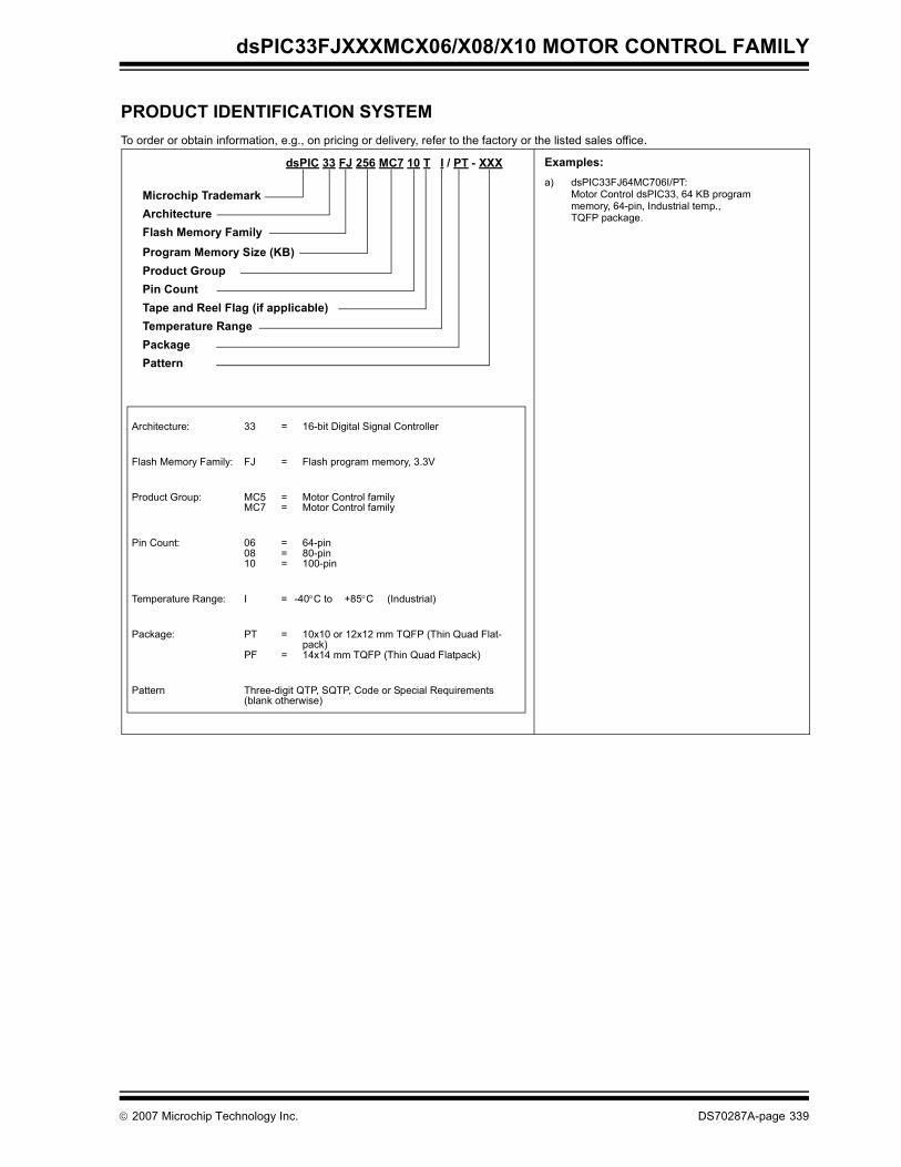
© 2007 Microchip Technology Inc. DS70287A-page 339
dsPIC33FJXXXMCX06/X08/X10 MOTOR CONTROL FAMILY
PRODUCT IDENTIFICATION SYSTEMTo order or obtain information, e.g., on pricing or delivery, refer to the factory or the listed sales office.
Architecture: 33 = 16-bit Digital Signal Controller
Flash Memory Family: FJ = Flash program memory, 3.3V
Product Group: MC5 = Motor Control familyMC7 = Motor Control family
Pin Count: 06 = 64-pin08 = 80-pin10 = 100-pin
Temperature Range: I = -40°C to +85°C (Industrial)
Package: PT = 10x10 or 12x12 mm TQFP (Thin Quad Flat-pack)
PF = 14x14 mm TQFP (Thin Quad Flatpack)
Pattern Three-digit QTP, SQTP, Code or Special Requirements (blank otherwise)
Examples:a) dsPIC33FJ64MC706I/PT:
Motor Control dsPIC33, 64 KB program memory, 64-pin, Industrial temp.,TQFP package.
Microchip TrademarkArchitectureFlash Memory FamilyProgram Memory Size (KB)Product GroupPin Count
Temperature RangePackagePattern
dsPIC 33 FJ 256 MC7 10 T I / PT - XXX
Tape and Reel Flag (if applicable)

DS70175F-page 284 © 2007 Microchip Technology Inc.
AMERICASCorporate Office2355 West Chandler Blvd.Chandler, AZ 85224-6199Tel: 480-792-7200 Fax: 480-792-7277Technical Support: http://support.microchip.comWeb Address: www.microchip.comAtlantaDuluth, GA Tel: 678-957-9614 Fax: 678-957-1455BostonWestborough, MA Tel: 774-760-0087 Fax: 774-760-0088ChicagoItasca, IL Tel: 630-285-0071 Fax: 630-285-0075DallasAddison, TX Tel: 972-818-7423 Fax: 972-818-2924DetroitFarmington Hills, MI Tel: 248-538-2250Fax: 248-538-2260KokomoKokomo, IN Tel: 765-864-8360Fax: 765-864-8387Los AngelesMission Viejo, CA Tel: 949-462-9523 Fax: 949-462-9608Santa ClaraSanta Clara, CA Tel: 408-961-6444Fax: 408-961-6445TorontoMississauga, Ontario, CanadaTel: 905-673-0699 Fax: 905-673-6509
ASIA/PACIFICAsia Pacific OfficeSuites 3707-14, 37th FloorTower 6, The GatewayHarbour City, KowloonHong KongTel: 852-2401-1200Fax: 852-2401-3431Australia - SydneyTel: 61-2-9868-6733Fax: 61-2-9868-6755China - BeijingTel: 86-10-8528-2100 Fax: 86-10-8528-2104China - ChengduTel: 86-28-8665-5511Fax: 86-28-8665-7889China - FuzhouTel: 86-591-8750-3506 Fax: 86-591-8750-3521China - Hong Kong SARTel: 852-2401-1200 Fax: 852-2401-3431China - QingdaoTel: 86-532-8502-7355Fax: 86-532-8502-7205China - ShanghaiTel: 86-21-5407-5533 Fax: 86-21-5407-5066China - ShenyangTel: 86-24-2334-2829Fax: 86-24-2334-2393China - ShenzhenTel: 86-755-8203-2660 Fax: 86-755-8203-1760China - ShundeTel: 86-757-2839-5507 Fax: 86-757-2839-5571China - WuhanTel: 86-27-5980-5300Fax: 86-27-5980-5118China - XianTel: 86-29-8833-7252Fax: 86-29-8833-7256
ASIA/PACIFICIndia - BangaloreTel: 91-80-4182-8400 Fax: 91-80-4182-8422India - New DelhiTel: 91-11-4160-8631Fax: 91-11-4160-8632India - PuneTel: 91-20-2566-1512Fax: 91-20-2566-1513Japan - YokohamaTel: 81-45-471- 6166 Fax: 81-45-471-6122Korea - DaeguTel: 82-53-744-4301Fax: 82-53-744-4302Korea - SeoulTel: 82-2-554-7200Fax: 82-2-558-5932 or 82-2-558-5934Malaysia - PenangTel: 60-4-646-8870Fax: 60-4-646-5086Philippines - ManilaTel: 63-2-634-9065Fax: 63-2-634-9069SingaporeTel: 65-6334-8870Fax: 65-6334-8850Taiwan - Hsin ChuTel: 886-3-572-9526Fax: 886-3-572-6459Taiwan - KaohsiungTel: 886-7-536-4818Fax: 886-7-536-4803Taiwan - TaipeiTel: 886-2-2500-6610 Fax: 886-2-2508-0102Thailand - BangkokTel: 66-2-694-1351Fax: 66-2-694-1350
EUROPEAustria - WelsTel: 43-7242-2244-39Fax: 43-7242-2244-393Denmark - CopenhagenTel: 45-4450-2828 Fax: 45-4485-2829France - ParisTel: 33-1-69-53-63-20 Fax: 33-1-69-30-90-79Germany - MunichTel: 49-89-627-144-0 Fax: 49-89-627-144-44Italy - Milan Tel: 39-0331-742611 Fax: 39-0331-466781Netherlands - DrunenTel: 31-416-690399 Fax: 31-416-690340Spain - MadridTel: 34-91-708-08-90Fax: 34-91-708-08-91UK - WokinghamTel: 44-118-921-5869Fax: 44-118-921-5820
WORLDWIDE SALES AND SERVICE
06/25/07