High Level VHDL Modeling of a Low-Power ASIC for a Tour...
102
High Level VHDL Modeling of a Low-Power ASIC for a Tour Guide by Umadevi Kailasam A thesis submitted in partial fulfillment of the requirements for the degree of Master of Science in Computer Engineering Department of Computer Science and Engineering College of Engineering University of South Florida Major Professor: Srinivas Katkoori, Ph.D. Murali Varanasi, Ph.D. Sanjukta Bhanja, Ph.D. Date of Approval: March 29, 2004 Keywords: Location-aware computing, Behavioral Synthesis, Leakage power, Translators, NAVIGATOR c Copyright 2004, Umadevi Kailasam
-
Upload
nguyendang -
Category
Documents
-
view
214 -
download
0
Transcript of High Level VHDL Modeling of a Low-Power ASIC for a Tour...

High Level VHDL Modeling of a Low-Power ASIC for a Tour Guide
by
Umadevi Kailasam
A thesis submitted in partial fulfillmentof the requirements for the degree of
Master of Science in Computer EngineeringDepartment of Computer Science and Engineering
College of EngineeringUniversity of South Florida
Major Professor: Srinivas Katkoori, Ph.D.Murali Varanasi, Ph.D.Sanjukta Bhanja, Ph.D.
Date of Approval:March 29, 2004
Keywords: Location-aware computing, Behavioral Synthesis, Leakage power, Translators,NAVIGATOR
c�
Copyright 2004, Umadevi Kailasam

DEDICATION
To my parents, family, and friends

ACKNOWLEDGEMENTS
I would like to thank Dr. Srinivas Katkoori for providing me the opportunity to be a part
of his research team. His constant encouragement and support provided me the confidence to do
this thesis work efficiently. I would like to thank Dr. MuraliVaranasi and Dr. Sanjukta Bhanja
for being on my committee. I would like to extend my special thanks to Viswanath Sairaman,
Narender Hanchate, and Ranganath Gopalan for helping me whenever I was stuck up with some
problem. I would like to thank my friends in the VCAPP group and outside, for providing me the
encouragement to do this good piece of work.

TABLE OF CONTENTS
LIST OF TABLES iii
LIST OF FIGURES iv
ABSTRACT vi
CHAPTER 1 INTRODUCTION 11.1 Motivation 11.2 Context-Aware Mobile Computing 21.3 Location-aware Computing 31.4 Design Flow of an ASIC 41.5 Power Dissipation is CMOS Circuits 6
1.5.1 Dynamic Power Dissipation 71.5.2 Short Circuit Power Dissipation 71.5.3 Leakage Power Dissipation 81.5.4 Proposed Approach 81.5.5 Thesis Organization 10
CHAPTER 2 LOCATION-AWARE MOBILE COMPUTING AND POWER OPTIMIZA-TION IN ASICS 11
2.1 Location-aware Mobile Computing 112.1.1 Personal Shopping Assistant 112.1.2 Location-based Agent Assistance 122.1.3 comMotion 132.1.4 Electronic Tourist Guide 142.1.5 CyberGuide 15
2.2 Power Optimization Techniques 172.2.1 Dynamic Power Optimization 17
2.2.1.1 Clock Gating 172.2.1.2 Precomputation 192.2.1.3 Guarded Evaluation 222.2.1.4 Retiming 242.2.1.5 Multiple Clocking 25
2.2.2 Leakage Power Optimization 272.2.2.1 Input Vector Control 272.2.2.2 Power Gating 282.2.2.3 Transistor Stacking 30
2.3 Summary 32
i

CHAPTER 3 MOBILE INTERACTIVE GUIDE 333.1 High Level Modeling of NAVIGATOR 33
3.1.1 GPS Receiver 353.1.2 USB Port 353.1.3 Flash Memory 353.1.4 Audio CODEC 35
3.2 Brief Description of the Flash Memory 353.2.1 FAT 16 Drive 38
3.3 Functionality of TOUR NAVIGATOR 393.4 NAVIGATOR Design 403.5 Design of Memory Module 443.6 Tools Used 44
3.6.1 High Level Modeling in VHDL 443.6.2 AUDI 453.6.3 SIS 463.6.4 Silicon Ensemble 483.6.5 Cadence Virtuoso Layout Editor 493.6.6 Translators 49
3.6.6.1 VHDL to KISS Translator 503.6.6.2 BDNET to Verilog Translator 503.6.6.3 VHDL to Verilog Translator 503.6.6.4 Steps to Generate the Layout 513.6.6.5 Functionality of Back-end Tool 51
3.7 Leakage Reduction Using Low-Leakage Standard Cells 543.7.1 Leakage-Delay Tradeoff 563.7.2 Summary 57
CHAPTER 4 EXPERIMENTAL RESULTS 584.1 Design Flow 58
4.1.1 Behavioral Level Simulation Results for the ASIC Design 594.1.2 Low-Leakage Standard Cells 60
4.2 Real World Applications 604.3 Layouts Generated by Back End Tool 644.4 Summary 64
CHAPTER 5 CONCLUSIONS AND FUTURE RESEARCH 685.1 Future Research 68
REFERENCES 69
APPENDICES 71Appendix A Behavioral VHDL Code of NAVIGATOR 72
ii

LIST OF TABLES
Table 2.1. Comparison of Proposed Approach with Previous Approaches 16
Table 4.1. Leakage Power Savings in Standard Cells 63
Table 4.2. Delay Overhead Due to Sleep Transistor in Standard Cells 63
Table 4.3. Leakage Power Savings in Real World Applications 63
Table 4.4. Area Overhead in Real World Applications 64
iii

LIST OF FIGURES
Figure 1.1. ASIC Design Life Cycle 5
Figure 1.2. Proposed Tour Guide 9
Figure 1.3. Model of Interface between NAVIGATOR and Flash Memory 9
Figure 2.1. Personal Shopping Assistant Service. Reproduced From [1] 12
Figure 2.2. Agent Interaction Diagram. Reproduced From [2] 13
Figure 2.3. Architecture of comMotion Showing the Three Different Modules. Repro-duced From [3] 14
Figure 2.4. Gated-Clock Architecture 18
Figure 2.5. Original Circuit 20
Figure 2.6. First Precomputation Architecture 20
Figure 2.7. Second Precomputation Architecture 21
Figure 2.8. Circuit without Guard Latches 22
Figure 2.9. Circuit with Guard Latches 23
Figure 2.10. Flip-flop Addition to Circuit 24
Figure 2.11. Repositioning the Flip-flops in a Pipeline 25
Figure 2.12. Original Circuit 25
Figure 2.13. Partitioned Circuit 26
Figure 2.14. Multiple Clocking Scheme 26
Figure 2.15. Modified Latches with Optimum Sleep Values (0 and 1) 28
Figure 2.16. MTCMOS Latch Circuit 29
Figure 2.17. Two Input NAND Gate. Turning “off” M1 and M2 raises �� to PositiveValue Causing the “Stacking Effect” 31
Figure 2.18. LECTOR Technique 32
Figure 3.1. Mobile Interactive Campus Tour Guide 34
iv

Figure 3.2. Overall Block Diagram of the System Design 34
Figure 3.3. Compact Flash Memory Card Block Diagram 36
Figure 3.4. Diagram showing the Pin Interface of NAVIGATOR with Flash Memory Card 40
Figure 3.5. Flowchart with Steps involved in the NAVIGATOR Design 41
Figure 3.6. Signals that Interface between NAVIGATOR and Flash Memory Card 42
Figure 3.7. RT Level Design given by AUDI 45
Figure 3.8. Controller State Machine in AUDI 46
Figure 3.9. Step to Design and Synthesize a Low Power System 52
Figure 3.10. Overall Data Flow Diagram of Synthesis of Design 53
Figure 3.11. Standard Cell with Sleep Transistor 55
Figure 3.12. Leakage Power Vs Transistor Width 56
Figure 3.13. Delay Vs Transistor Width 56
Figure 4.1. Behavior of ASIC when ‘go’ Signal is Asserted 61
Figure 4.2. Serial Audio Data Output when there is a Match 62
Figure 4.3. Generated Layout for IIR Filter 65
Figure 4.4. Generated Layout for DCT Application 66
Figure 4.5. Generated Layout for FFT Application 67
v

HIGH LEVEL VHDL MODELING OF A LOW-POWER ASIC FOR A TOUR GUIDE
Umadevi Kailasam
ABSTRACT
We present the high level (VHDL) modeling and high level synthesis of an ASIC (TOUR
NAVIGATOR) for a portable hand held device - a tour guide. Thetour guide is based on location-
aware mobile computing, which gives the information of the current location to the user. The
TOUR NAVIGATOR designed in this work is interfaced with off-the-shelf components to realise
the tour guide system. The current location is given by an on-board GPS receiver chip. The
TOUR NAVIGATOR is a search and play module which interfaces with the flash memory, GPS
receiver and the audio codec. The functionality of the TOUR NAVIGATOR is to search the flash
memory for audio data corresponding to the current GPS co-ordinate, which is an input to the
TOUR NAVIGATOR. The look-up table containing the GPS coordinates and the corresponding
audio files are loaded into the flash memory, where in each GPS entry in the table is indexed by the
co-ordinates, and an audio file that contains information about the locations is associated with it.
When there is a match, the audio file is streamed to the codec.
The functionality of the interface of the TOUR NAVIGATOR with the memory module is verified
at the RTL using Cadence-NCLaunch. The layout implementation of the TOUR NAVIGATOR is
done using an automatic place and route tool (Silicon Ensemble), which uses standard cells for the
entire design. Leakage power reduction is done by introducing sleep transistors in the standard
cells. The TOUR NAVIGATOR is put into a “sleep” mode when there is no operation of the tour
guide, thus giving significant power savings.
vi

CHAPTER 1
INTRODUCTION
In recent times mobile applications such as hand-held devices, PDA, etc. have gained wide
acceptance allowing the user to move around with computing capability and network resources.
Many devices that are recently developed are conceived withmobile capability as their primary
objective. Performance is the main focus of these applications, where response time is the major
objective. Such is the case with processors which are mainlybuilt for speed and performance. Other
applications such as inexpensive mobile chips that are widely used mainly focus on functionality
rather than performance. The specific function performed bythe device not typically found in
processors or devices based on performance, becomes the need for the user. In the context of
context-aware computing, we develop an application that isfocused on functionality desired by the
user by trading off with performance.
1.1 Motivation
Mobile computing is a rapidly evolving field that gives the user the power and potential to
access any information on the move. Nowadays web browsing iscarried out via mobile devices.
The reduction in the use of applications and computers in a static environment has led to a enormous
change in trend in the domain of mobile computing. Dynamic environment has become a major
area of research to improve the quality of mobile applications that enable users to access any kind
of information from any location. In such an environment, the physical connections between the
host and the network to be connected should be constantly recomputed. Today’s technology and
software progresses must adapt to such a constantly changing behavior of the system.
All the mobile applications are based on the concept of context-aware computing, which is
characterized by the ability of an application to adapt its behavior to the constantly changing envi-
ronmental factors with least control over them. Today’s improvement and advances in technology
1

and software is enabling easier adaptation to the changing user’s requests and environment. The
contextual information that is exploited in such applications are the user’s location, the physical
factors and informations surrounding the user, the user’s current activity and the time of the day.
However there is a constraint on the user’s request to obtaininformation pertaining to the user’s
location and wireless communication.
VLSI design technology has advanced at a high level in the implementation of mobile devices,
with high performance and low power dissipation at an optimal cost. It provides the ability to
integrate mixed, analog and digital signals on a single chip. There is scope for an entire mobile
application to be realized on a single chip. To realize theseapplications, it is important to have a
system to convert a large number of behavioral description of these mobile devices with various
user’s needs and requests, into its physical implementation without much of user intervention in
the middle stages.
Hence the motivation of this work, is to provide the user witha specific functionality that is
based only on his location and to realize the physical implementation of it with no user interven-
tion. The following sections give an overview of the concepts and features used in developing this
application.
1.2 Context-Aware Mobile Computing
Portable computers and wireless communication devices have become a major part of our day-
to-day life enabling people to access their personal information, public resources, and corporate
data at any time in any location. Context-aware computing isa mobile computing paradigm [4]
in which applications can discover and take advantage of contextual information. The contextual
information that is primarily available for designing systems are, entity, location, time, and activity
of the user. These informations enables the applications topredict the present situation and sur-
rounding environment of the user to provide him with more services. Schilit [5] gives definitions
for context-aware applications as follows :
1. � ����� ��� ������� : This is a technique of user-interface where the location ofnearby
objects are emphasized.
2

2. �� ��� ���� ��������� � ����� ���������: This is a process, where new components are
added by removing the existing components or by altering theconnections between components
due the change in context.
3. � �������� ��� ��� ����� ��� �������: This depends on the context in which they are
issued and produces different results accordingly.
4. � ������ � �� ��� �� �� ������: These are simple rules which emphasize on how the context-
aware system should adapt to the context.
Chen gives a different perspective on how a mobile application should take advantage of avail-
able context and gives two definitions of context aware computing [4]:
� ���� � ������� �� �� ���: an application automatically adapts to discovered context, by
changing the application’s behavior.
� ��� � ������� �� �� ���: an application presents the new or updated context to an inter-
ested user or makes the context persistent for the user to retrieve later.
Given a context, whether active or passive, it depends on howthe context is used in the ap-
plication. Efficient use of the current available contextual information in applications is still a
challenging problem in developing applications. Active context-aware computing is interesting
and important as it paves way for the design of new mobile devices that require more infrastructure
support. In this work, we focus on designing an application that provides services by sensing the
location (active context) of the user
1.3 Location-aware Computing
The user’s location plays a significant role in implementingsuch portable devices. Location
awareness is an emerging trend in mobile computing. Location is an important context that has to
be updated whenever the user makes a move. This leads to a needfor a reliable position-tracking
system which is a critical component of many context-aware applications.
Location awareness is taken advantage by systems that are aware of where they are located.
There are two types of techniques to obtain location awareness [6], namely,��� ��, and� ����� �positioning. Applications using absolute positioning areaware of the actual location: either the co-
ordinates or the building, city, or country of the user. GPS (Global Positioning System), GSM
3

(Global System for Mobile communication together with MPS(Mobile Positioning System) [6] are
some technologies used for absolute positioning. Relativelocation on the other hand, is aware of
what other objects are in close proximity. When using relative positioning in an application, the
objects can be moved around. The system should recognize other objects without depending on
where the device is located.
The location of the user must be deciphered by sensing on whether the user is outdoor or indoor.
The most common choice for outdoor positioning system is theGlobal Positioning System (GPS).
The GPS signal does not work indoor as the signal strength is too low to propagate through the
buildings. It is a challenging problem to build an indoor location sensor that provides fine-grain
information at a high update rate. Few applications such as the Personal Shopping Assistant [1]
developed at the Hewlett-Packard Laboratories, is based onthe Radio Frequency Identification
(RFID) technology which allows the reading of specific labels attached to products and packages
by means of radio signals. The CyberGuide project [7] has built an indoor tracking system based
on infrared (IR).
1.4 Design Flow of an ASIC
The main stages in the design cycle for an ASIC are design entry, functional simulation, physi-
cal layout, test simulation, and design verification beforereleasing the design for fabrication. These
stages are the same irrespective of the technology used in the ASIC design. A CAD system pro-
vides a suite of facilities [8] and steps that are integratedto support all these stages with a proper
combination of automatic and user-controlled processing at each stage. The CAD system has de-
fault options at many stages, which the designer may choose or ignore if necessary at each stage.
The entry format given for a design to the CAD system is compiled to a set of schematics or a pro-
gram in a hardware description language (HDL), to an intermediate design language (IDL) that is
used for simulation and physical placement. The physical placement process comprises of several
steps that leads to a layer-by-layer description of the ASICnetwork.
Power consumption has become an important parameter along with area, speed and testability
in the design of VLSI circuits. Today’s ASIC Designers are facing a common dilemma with the
product specification in one hand that states that the designmust consume the minimum power
4

Figure 1.1. ASIC Design Life Cycle
requirements so as to meet the goals of reliability, cost andenergy efficiency, and the functional
specification on the other hand which implies that the ASICs must integrate more circuitry and
the speed should be faster to implement the desired functionality, that increases the overall power
consumption. A decade ago, when power consumption was not the major constraint ASICs were
designed with more importance to speed and design constraints as large packages, cooling fans and
fins have been capable enough to dissipate the generated heat. The difficulty in providing the neces-
sary cooling due to the increase in chip density and chip sizemay result in significant cost overhead
or limit the system functionality that can be provided. Thismakes the need of a high-throughput,
low-power digital systems very evident. Today’s designers, due to the unavoidable necessity to re-
duce power consumption adopt design methodologies and techniques at different abstraction levels
to reduce power consumption. These abstraction levels are at technology, circuit, logic, architec-
ture and system. Substantial minimization of power consumption requires power-aware decisions
that are made at each level of design abstraction. MOS technology has scaled down to 0.2 micro
minimum feature size that increases the possibility of placing 1 X ��� transistors in an area of 8
5

in x 10 in if a high-density technology is used [9]. For high-performance microprocessor, an in-
crease in the amount of on-chip memory would best utilize theincreased capability of transistors.
The proliferation of personal digital assistants and portable devices has increased the demand of
designing low power ASICs. High performance and low-power consumption has become a major
problem confronted by most portable devices. Energy minimization is one of the most important
metrics in the design of a portable system. The battery capacity plays a major role in the power
consumption of portable systems. It has improved at a very slower rate (a factor of two or four) in
the past 35 years where the computational demands have increased drastically over the same time.
Hence portable systems are highly power-constrained with an effort to increase the battery life and
reduce the battery weight. Another important consideration that should be taken into account in
portable applications is that many computation tasks are real-time such as speech recognition that
always requires the computations at near-peak rates. The conventional way of shutting down the
power is not an appropriate solution for such applications that always require active computations.
The degree of freedom in design that is available in implementing these functions is that as the real
time requirements of these applications are satisfied, there is no effect in increasing the computa-
tional throughput. This fact along with the unlimited number of transistors that can be used, leads
to developing an architectural design that can show significant savings in power dissipation.
1.5 Power Dissipation is CMOS Circuits
The three major sources of power dissipation in CMOS circuits are represented by the following
equation:
� ����� � � �� ����� � � �� � �� ���� � � ������� (1.1)
� � � ��� �� ���� ����� � � ��� ���� � �������� ���� (1.2)
The first term denotes the switching component of power, which is due to the switching tran-
sient current and the charging and discharging of load capacitances.�� is the loading capacitance,
���� is the clock frequency,��� is the supply voltage, V is the voltage swing that is the same as that
of the supply voltage, and� � is the activity factor that gives the probability that a power consuming
transition occurs. The second term denotes the direct-pathshort circuit current��� which is current
6

that flows from the supply to ground when both the PMOS and the NMOS transistors are simulta-
neously turned ON. The third term denotes the leakage current, ��������, which is due to the reverse
bias leakage between diffusion regions and the substrate, and sub-threshold conduction. The first
term contributes to dynamic power dissipation and the second and third terms contribute to static
power dissipation.
1.5.1 Dynamic Power Dissipation
The switching activity in a CMOS circuit that gives rise to the dynamic component of power
consumption is when the PMOS transistors charge the load capacitance�� to make a transition
from 0 to ��� which is the highest voltage level. On the vice versa, for the��� to 0 transition
at the output, there is no charge that is drawn from the supply, the stored energy in the capacitor
is dissipated in the pull-down NMOS transistor. The power drawn from the supply is given by
�� � ��� ���� if the transitions occur for a clock frequency of���� .From the equation (1.2), it is seen that power dissipated is proportional to the square of the
supply voltage. Hence the most direct way to reduce power is by reducing the supply voltage. A
reduction in the voltage by a factor of two results in the reduction of power by a factor of four. The
disadvantage in this method is that the circuit delay increases considerably.
1.5.2 Short Circuit Power Dissipation
There is a direct current path between the supply and ground during finite rise and fall times
that exists for a short period of time during switching. Thiscondition arises when both the NMOS
and PMOS devices are simultaneously ON creating a conductive path between the��� and GND.
This current is significant when the input rise or fall time ata gate is greater than the output rise
or fall time. Due to this, the short circuit path will be active for a long time period. To reduce the
short circuit current, it is desirable to make the input riseor fall time equal to the output rise or fall
time. This reduces the short circuit power consumption to beless than 10% of the total dynamic
power of the circuit. The short circuit current can be eliminated by lowering the supply voltage
lower than the sum of the thresholds of the transistors, as both the NMOS and PMOS devices will
not be in the “ON” state for any input values.
7

1.5.3 Leakage Power Dissipation
The leakage current is due to the reverse-bias diode leakageon the drain of the transistor and the
sub-threshold leakage current that flows through the channel of an off device. Consider an inverter
which is given a input ‘1’. This turns on the NMOS transistor giving ‘0’ as output. Though the
PMOS transistor will be turned off, the bulk of PMOS will be at��� and the drain-to-bulk voltage
will be equal to -��� . This leads to a current that is the product of the area of the drain diffusion and
the leakage current density and less dependent on the supplyvoltage. The leakage current due to
diode leakage becomes significant when the system is idle fora long time as this power is dissipated
though there is no switching. The leakage power due to sub-threshold leakage current occurs when
the gate to source voltage is greater than the weak inversionpoint, but below the threshold voltage
� �, there is a carrier diffusion between the source and drain. Hence, an optimal� � is chosen for
low voltage applications that controls the sub-threshold voltage.
1.5.4 Proposed Approach
The proposed approach is the design of a location-aware based tour guide which has the in-
formation about all the locations of a tour plan. The Global Positing System (GPS) is used as
the tracking component to locate the current position of theuser. The system does not depend on
communication with any external server. The device shown infigure 1.2. is built by integrating off-
the-shelf components like, GPS receiver, Flash memory, ASIC, USB interface, and audio CODEC.
The search and play module is implemented as an ASIC which interfaces all these components to
perform the functionality. Depending on the GPS co-ordinates of the current location, the ASIC
searches the audio data corresponding to that location in the Flash memory card to play out the
audio information to the output.
The behavior of the ASIC and the Flash memory is modeled in thehigh level using VHDL
to ensure the correctness of the functionality as shown in figure 1.3.. The data to be accessed
in a similar fashion as in a solid state flash memory that uses FAT16 file system. This design is
synthesized using AUDI (Automatic Design Instantiation) synthesis system which is a behavioral
synthesis system, capable of synthesizing such control intensive applications into the corresponding
RT level design.
8

USB Interface
AUDIO
START MemoryFlash
ASIC
Codec
AudioReceiver
GPS
Figure 1.2. Proposed Tour Guide
NAVIGATOR(VHDL)
FLASH
MEMORY
(VHDL)
DATA IN
TEXT FORMAT
Figure 1.3. Model of Interface between NAVIGATOR and Flash Memory
9

The validation of this design is done at the RTL using CadenceNCLaunch. A back end tool is
built to convert the RTL synthesized output given by AUDI to the transistor level physical imple-
mentation of the design.
Leakage power for this mobile device is controlled by use of sleep transistors. Introduction of
sleep transistors in the standard cells in the standard celllibrary, that is used to place and route the
design, the leakage power of the entire design is minimized considerably with minimal delay. A
technique to reduce the leakage power by use of sleep transistors in the controller design generated
by AUDI is also proposed.
1.5.5 Thesis Organization
In Chapter 2, the related work area in the area of context-aware computing and logic level power
optimization is discussed. In Chapter 3, the approach to design and implementation of ASIC with
leakage power reduction is presented in detail. In Chapter 4, the experimental results is discussed.
In Chapter 5, the conclusion of thesis with future work is discussed.
10

CHAPTER 2
LOCATION-AWARE MOBILE COMPUTING AND POWER OPTIMIZATION IN ASICS
We present a detailed survey of some of the prior work done in location-aware mobile comput-
ing, logic level and RTL power optimization (Dynamic power and Leakage power) techniques that
have been proposed to reduce power dissipation in the logic level and RTL level. We also present
in detail the novelty of the proposed application in mobile computing in comparison to the existing
applications. The power optimization technique that is chosen to obtain the best power savings for
the proposed application is discussed in the next chapter.
2.1 Location-aware Mobile Computing
Mobile computing has stimulated a radical revolution, changing our day-to-day lives with the
use of popular small hand held devices such as PDAs, Pocket PCs etc, which are embedded with
substantial processing capabilities. Location is a very important context in most of the mobile
applications. In the following section, we describe some ofthe applications that are based on
location-aware computing.
2.1.1 Personal Shopping Assistant
The PSA [1] is a hand-held wireless communication device which the customer owns (provided
by the shopping center) and a centralized server located in the shopping center to which the cus-
tomers can communicate. The server maintains the store and product database, customer profile,
and provides audio and visual output for the customer’s inquiries over a wireless network.
The PSA consists of two components, namely, the PSA unit which is a small and low-cost
device acting as a terminal for communication and the PSA server which is the heart of the PSA
system.
11

RF CEILING NODES
PSA UNIT PSA UNIT
Corporate IQOther Stores and
SERVERASSISTANTSHOPPING
USERUSER
Figure 2.1. Personal Shopping Assistant Service. Reproduced From [1]
1. � �� � ���: The PSA is different from the PDA not only in its set of input/output inter-
faces but also in its functionality that is entirely dependent on its server. The PSA relays
information to and from the PSA server. The microprocessor of PSA processes the protocols
that is involved in setting up a virtual circuit with the server, directs messages to the output
devices, perform compression/decompression on audio input/output, tags messages from the
input devices before transmitting to the wireless interface.
2. � �� � ��� �� : The PSA server takes the responsibility to provide the functionality of answering
to the queries placed to the PSA unit. Once the connection is established, the server uses that
identifier to retrieve the customer’s profile from its database and aid in the queries placed by
the customer. The transmitter and receiver form the wireless network subsystem that sends
and receives voice and images to and from the PSA units.
2.1.2 Location-based Agent Assistance
This application approaches location-based computing [2]by communication with four com-
ponents, namely, the User Agent, the Wherehoo server, Provider Agents, and Providers. The User
Agent issues a query consisting of the location, search radius and keywords representing the user’s
interest and interacts with the Provider Agents, the Wherehoo server is a search server that searches
using the location as its primary input and the keywords as its secondary input. Businesses, ser-
12

vices, attractions etc., registered with the Wherehoo server and have internet presence form the
Providers. The Provider Agents are controlled by the Providers and interact with User Agents.
Wherehoo server
A
B
C
A
B
C
Provider Agents Providers
User Agent residing in
the hand-held device
USER
Figure 2.2. Agent Interaction Diagram. Reproduced From [2]
The display device used by the User is a� ���� � computing appliance that is equipped
with GPS receiver. It has a wireless Internet connection. Anagent in the device keeps construct-
ing queries in the background depending on the user’s needs,queries and communicates with the
Wherehoo server. The Provider Agents, depending on the user’s wants, retrieve and filter data
according to the user’s wants. The user’s queries are obtained from the user through form-based
applications on the Palm device. Series of alerts and place listing is used by the agent to interact
with the user. The Wherehoo server is a search engine that returns XML documents taking the
GPS coordinates, search radius, and keywords as input from the user, geographic location of each
Provider’s service and a description of how to process the query of each of the Provider Agents.
The User issues direct queries after selecting the Providerthat matches his interest in the form of
URL’s.
2.1.3 comMotion
comMotion [3] is a location-aware computing environment, which reminds the user of their
duties depending on the user’s current location, providingboth geographical and speech interfaces.
comMotion takes in the GPS coordinates (latitude and longitude) and translates them into positions
13

that are relevant to the user. It has a to-do list for the user depending on the location in the form of
voice and text entries. On obtaining the location from the user, the to-do list is associated with it
which alerts the user that he has items to be performed in the current location.
ReceiverGPS
CDPDModem
physical
messages
virtual
location
direct and indirect
feedback
GPS satellite
system
main message server
map server info server
Internet
position query
position info
location
context-related
message USER
Query Engine
Location Learning Agent
Message Engine
Figure 2.3. Architecture of comMotion Showing the Three Different Modules. Reproduced From[3]
The hardware of comMotion includes a GPS receiver, a portable PC, a CDPD modem, and a
Jabra earphone speaker with a microphone. The client side uses both graphical and speech inter-
face. Speech recognition and text-to-speech synthesis wasdeveloped using AT & T’s Watson SDK
(Software Development Kit). Automatic Speech Recognition(ASR) and Text-to-Speech (TTS)
synthesis system in integrated into the Watson product which uses phoneme-based sub-word anal-
ysis supporting speaker independence and continuous speech. TCP/IP sockets are used on the
client side to communicate to all the different server processes, to provide easy transfer of these
process to the client device with Web-server capabilities.
2.1.4 Electronic Tourist Guide
The GUIDE System [10] developed by the distributed multimedia research group in Lancaster
University, supports navigation and information needs of visitors to the city of Lancaster using
wireless communications, context-awareness, and adaptive hyper-media. It uses a cell based wire-
less communication infrastructure to broadcast positioning information and user’s needs to portable
14

GUIDE units that run a customized web browser. The GUIDE units obtain positioning information
by receiving location messages that are transmitted from strategically positioned base stations.
The GUIDE system is based on distributed and dynamic information model that is sent to
portable hand-held GUIDE units. Considering the end systems to be used in the GUIDE unit
as pen-based tablet PCs and PDAs, the gray-scale transflective version of Fujitsu Teampad was
selected, which is based on Pentium 166 MMX processor. The city contains a number of WaveLAN
cells, which conform to IEEE 802.11 standard and each cell proves a shared bandwidth which is
supported by a GUIDE server. The information model represents the geographic information by
including special navigation point objects that are used inconjunction with the location objects to
determine the best route between a source and a destination.Each GUIDE unit can locally cache
parts of the information model and therefore operate even when the network is disconnected.
2.1.5 CyberGuide
Tourism is the application domain of CyberGuide [7] developed by Georgia Institute of Tech-
nology. The main objective is to know where the tourist is, give information and answer the tourist’s
queries about the location by use of PDAs and pen-based PCs using RF for indoor positioning and
GPS for outdoor positioning.
The system is divided into several independent components so as to make it useful for the
tourists in terms of generic function. Overall the system gives the appearance of a single unit as a
tour guide. Apple MessagePad 100 with Newton 1.3 is used and pen-based PCs running Windows
for Pen Computing 1.0. Let us take a look at the different components of CyberGuide.
1. � �� ��� ��� ��� : This is the map component of the system. This component has knowledge
about the physical surroundings like the location of buildings or routes which the tourists can
access. This system realizes this component by a map of the physical environment visited by
the tourist.
2. � ���� ���: This is the information component of the system which givesall the information
about the sights that a tourist might encounter during theirvisit such as descriptions of the
building. This is considered as the structural repository of information.
15

3. � �� ������ : This is the positioning component of the system to show the immediate nearby
surroundings on the map and gives answers about these surroundings. This component is
realized by a positioning module that gives exact information about the current location of
the tourist so that navigator can chart the nearby locationsclose to the current location.
4. � ���� �� : This is the communication component of the system for the tourist to send
and receive information acting like a messenger service. The tourist can communicate with
the central service locate the others. This component is realized using a set of wireless
communication services.
In Table 2.1. we provide the comparison of our proposed work with the applications discussed
in the previous work.
Table 2.1. Comparison of Proposed Approach with Previous Approaches
Application Purpose Context User External ComponentsMobility Communication Used
Cyberguide Guidance for Tourist Within Yes PDA and GPS(Georgia for tourist location Georgia Tech unit
Tech) in labs and and time campuscomMotion Guidance for Tourist Within Yes Portable PC,
for tourist location exhibition GPS receiver,in exhibition and time DPD modem
Impulse Answer queries User Anywhere Yes Palm with(MIT lab) to explore location GPS receiver
physical worldPersonal Services to Customer Shopping Yes Plessey ARM610 ,Shopping customer in location center and Sparc 10sAssistant shopping centerElectronic Guide for Tourist Lancester Yes Fujitsu Teampad
Tour Tourists in location City 7600Guide Lancester CityTour Guidance for Tourist Anywhere No Off-the-shelf
Guide pre-stored location components (GPSTour plan as receiver,Flash
desired by User memory, Audiodesired by User code and ASIC)
16

2.2 Power Optimization Techniques
Extending the battery lifetime of the batteries used for themobile devices is the major chal-
lenge. Power is a critical and shared system resource. Optimization techniques for obtaining low
power can be applied at many different levels of the design hierarchy. Optimization at the logic
level has been shown to have a very significant impact on the dissipation of power of combinational
logic circuits. In this section, we review some of the power optimization techniques that are applied
at the logic level.
2.2.1 Dynamic Power Optimization
In the following sections we discuss some of the techniques used for dynamic power optimiza-
tion.
2.2.1.1 Clock Gating
In synchronous circuits, selectively stopping the clock inportions of the circuit where there
is no active computation is a very efficient technique to reduce power dissipation. Benini and
De Micheli [11] have proposed this technique to reduce the switching activity of the circuit that
leads to power dissipation during the idle periods. The mainidea behind this work is to detect the
idle period of the circuit from the state diagram. In the caseof Moore machines, the idle period
is identified by detecting the self-loops. In [11], the limitation to Moore finite-state machines
has been removed by proposing a new method. It deals with a very general model of sequential
circuit, the incompletely specified Mealy machine and a novel probabilistic approach, that can
selectively separate and exploit the idle conditions that occur with high probability. This is done
by transforming the Mealy machine into an equivalent Moore machine.
Local clocks that are conditionally enabled are called gated clocks, because a signal from the
environment is used to qualify the global clock signal [11].An edge-triggered flip-flop followed by
a combinational logic with a single clock is assumed in the Figure 2.4.(a). It has been modified with
a gated clock implementation in Figure 2.4.(b) with a new signal called the activation function��whose sole purpose is to stop the clock when there is no state transition in the finite state machine
and the machine is in an idle state. The block L in Figure 2.4.(b) is used to filter out the glitches
17

OUT
CLK
STATE
IN LogicCombinational
Registers
(a)
Combinational
Logic
Registers
STATE
CLK
OUTIN
GCLKL &
af
(b)
Figure 2.4. Gated-Clock Architecture
18

on �� to ensure a correct behavior. When the activation function�� becomes high, the finite state
machine is not clocked. The authors have proposed a technique [11] that automatically generates
the activation function in form of a combinational logic block that uses as its inputs the primary
input IN and the state lines STATE of the finite state machine.This technique is strongly dependent
on two factors - how much of state splitting is needed to transform the machine to a locally Moore
machine. It also depends on the self loop conditions, the time for which the finite state machine
will be in the self-loop condition and to generate the activation function that is not minimal. In
this technique [11], by shutting down the local clock in portions of the circuit that are idle reduces
the power consumption as no power is consumed in the finite state machine, combinational logic
and the sequential circuits. The drawback of this techniqueis that the additional circuitry for the
computation of the activation function�� is an overhead and increases the delay if it is in the
critical path of the circuit. And for machines that have a very small number of self loops, the area
of improvement is almost null [11]. The gated-clock technique is very advantageous for circuits
that are idle for a long time and get activated by START signals. To implement this technique,
knowledge of the environment is required in terms of activity so as to indicate if the activation
function should be high or low.
2.2.1.2 Precomputation
This method deals with the problem of reducing the power by optimizing logic-level sequential
circuits. Alidina �� � [12] proposed a powerful sequential logic optimization method to reduce
power that is based on selectively precomputing the output logic values of the circuit one clock
cycle before they are required, and using the precomputed values to reduce internal switching
activity in the succeeding clock cycle. The main objective of this technique is to synthesize the
precomputation logic, which predicts the output of a subsetof inputs for the next value. The
original logic circuit can be switched off in the next clock cycle by using a latch if the outputs can
be precomputed using the precomputation logic. The precomputation logic takes as its inputs the
current inputs of the circuit and computes the output value.The important factor in this method
is that the power savings that are achieved by implementing this technique should overcome the
19

power that is dissipated by the additional circuitry that isadded for the precomputation logic to
select the inputs for which the output is precomputed.
f
nx
x2x1
AR1 R2
Figure 2.5. Original Circuit
Two registers separated by a combinational logic block is given in Figure 2.5.. It is assumed
that block A computes and outputs a Boolean function� . The two predictor functions g1 and g2
predict the output value of the combinational block A for thenext clock cycle as given below:
�� � � �� � �� � �� (2.1)
�� � � �� � �� � � � (2.2)
During the clock cycle t, if g1 evaluates to 1, the input to theregister R2 in the succeeding clock
cycle is a 1 and if g2 evaluates to a 1, then the input to the register R2 in the succeeding clock cycle
is a 0. If either g1 or g2 evaluates to 1, the register R1 is disabled i.e, that in the succeeding clock
cycle the inputs to block A do not change.
� �� �� ��
� �� �� �� �
� � � � �g1
g1g2FF
FF
R2R1
x1x2
xn
A
f
LE
Figure 2.6. First Precomputation Architecture
20

The authors of [12] has proposed two precomputation architectures. In the first precomputation
architecture seen in Figure 2.6., the predictor function isevaluated by a subset of the inputs which
predicts the output value of the circuit in the next clock cycle. If the output value is predicted then
the inputs to the combinational block A do not change and thisoutput value is used in the next
clock cycle, thus reducing the switching activity in the combinational block A. The main objective
of this method is to use the minimum number of inputs to predict the output in order to avoid
the duplication of the combinational block A and to avoid theincrease in power due to the area
overhead. At the same time, the chances of predicting the output should also be maximized. This
leads to the second precomputation architecture as shown inFigure 2.6.
A R3
R1
f
g1
g2
x1x2
xnR2LE
Figure 2.7. Second Precomputation Architecture
In the second precomputation architecture [12], the inputsto the combinational block have been
split into two sets that correspond to the registers R1 and R2. The combinational block A is fed
continuously by the register R1 with the inputs that are usedto predict the output value for the next
clock cycle. If the predictor logic predicts the output value for the next clock cycle, the Register
R2 is blocked and there is no switching activity among the inputs to the combinational block A.
This reduces some switching activity in the internal nodes of block A.
Precomputation technique aims at reducing the switching activity in the circuit in the con-
secutive clock cycles by predicting the output. This technique increases the circuit area and can
affect the circuit performance resulting in an increased clock period due to the delay caused by
the predictor logic circuit. And moreover this technique isdependent on previous input history.
21

This technique is applicable for circuits that are specific on application with their environment
information known priorly.
2.2.1.3 Guarded Evaluation
Vivek Tiwari �� � [13] proposed a method for power optimization in a similar manner as clock
gating and precomputation. The method is an application of power management at the logic level.
The technique determines, the parts of the circuit that perform useful and useless computation and
shuts down the parts of the circuit performing useless computation per clock cycle. Transparent
latches are used with ENABLE signal is used to disable the clock of the components that perform
useless transitions. The ENABLE signal is calculated from asubset of existing input signals that
does not affect the primary output of the module when blocked.
Data Register Data Register
Shifter Adder
MUX c
0 1
Figure 2.8. Circuit without Guard Latches
In Figure 2.8., the ALU performs both shifting and addition operations every clock cycle. The
result of one of these is selected using a multiplexer. The evaluation of both the operations is
unnecessary every clock cycle as the result of only one of theoperations is taken to the output. If
the decision is made as to which of the results of the two operations is needed, the computation
of result by the other component can be avoided leading to significant power savings. In Figure
22

2.9., guards which are transparent latches with an enable input are placed at the inputs of those
parts of the circuits that need to be selectively turned off.If the module has to be active, the enable
signal in the guard allows inputs to propagate through the transparent latches permitting normal
operation. If the module has to be inactive, the transparentlatch retains its previous value and
there is no computation or transition performed in the module. On an abstract level, in a CMOS
circuit, the primary input causes the primary output to change which is the result of switching of a
large number of gates where all the switching activity is unnecessary. For example, in the case of
a two-input AND gate with one of the inputs already set to 0, any switching activity in the other
input does not affect the output. Hence the switching activity on the second input is useless and
can be blocked.
Shifter Adder
MUX c
0 1
Data Register Data Register
L1 L2Guard Logic
c=0 c=1
Figure 2.9. Circuit with Guard Latches
The author states that their technique is different from precomputation in that the entire circuit
need not be re-synthesised to find out the possibilities as towhen the circuit has to be shut down.
The evaluation of the sub-circuit that is used to shut down the modules is guarded by the existing
input signals of the circuit. In other words the circuit is never clocked OFF. Hence there is no ne-
cessity to resynthesise the circuit. The power optimal inputs to the circuit are obtained by including
a transformation circuitry to the original circuit.
23

2.2.1.4 Retiming
Monteiro �� � proposes a technique in [14] to reduce power dissipation in sequential circuits
such as pipelines. A pipelined sequential circuit can be acyclic corresponding to blocks of com-
binational logic that are separated by flipflops. The introduction of a flipflop to a combinational
block reduces the switching activity at the output of the block leading to lower power dissipation.
GCL
(a)
G R
CL
(b)
Figure 2.10. Flip-flop Addition to Circuit
In Figures 2.10.(a) and 2.10.(b) the power dissipated by thecircuit is given by� � and � � ,
where� � is the average switching activity at the output of the gate G and� � is the load capacitance.
When a flip-flop R is introduced at the output of gate G, the power dissipated by the gate G is given
by � � � � � � � � � , where� is the capacitance at the input of the flip-flop and� is the
switching activity at the output of the flipflop. The observation here is that� � � � as the output
of the flipflop makes at most only one transition per clock cycle whereas gate G may make three
transitions for the same. Hence the addition of flip-flops to acircuit decreases power dissipation. In
a similar way, repositioning of a flip-flop in a pipeline according to the amount of spurious activity
at various stages of a pipeline, leads to reduction in power.
The authors propose an algorithm to place a flip-flop at the output of a selected set of nodes
as shown in Figure 2.11.. This leads to reduced switching activity reducing the power dissipation
in a pipelined circuit. The selection of nodes is done based on the amount of glitching activity at
the output of these nodes. A cost function is given by estimating the average switching activity of
the combinational network both with zero delay and actual delay for each gate, thus calculating the
amount of glitching at the output of the nodes and the probability [5] that a transition at each gate
propagates through its transitive fanout. This method reduces the consumption of power without
any loss in performance.
24

P0 P1 P2FF
P0 FFP1 P2
Figure 2.11. Repositioning the Flip-flops in a Pipeline
2.2.1.5 Multiple Clocking
Papachristou�� � proposes a technique in [15] to design low-power register-transfer-level
datapaths. A circuit is partitioned into� disjoint modules and each module is assigned a distinct
clock. The technique uses� non-overlapping clocks by dividing the frequency� of a single clock
into � cycles. In this way each module operate only during its duty cycle and power is reduced as
the clocking frequency of each module is� ��. The overall frequency of the circuit remains the
single clock frequency� . This way the modules that are inactive are turned off duringtheir off
duty cycle reducing the power dissipation.
a d c b
x , y , z
e
x , y , z u , v , w
+ − + −
Figure 2.12. Original Circuit
25

The differences in the circuits Figures 2.12. and 2.13. are (1) circuit 1 needs less resources
than circuit 2. (2) The two ALUs in circuit 1 use a single clockand work concurrently. Whereas
in circuit 2, the circuit is partitioned in a way that the firstsub-circuit works during the odd time
steps and the second sub-circuit works during the even time steps. Allocating the nodes at even
and odd time steps partition the circuit into separate sub-circuits that are active at non-overlapping
time intervals, making the use of non-overlapping clocks.
− + +
d
e b a
c
x , u y , v z , w
CLOCK1 CLOCK2 CLOCK3
T1 T3 T5 T2 T4 ..... T1 T3 T5
Figure 2.13. Partitioned Circuit
Figure 2.14. shows the two non-overlapping clocks whose frequency is� ��, where� is the
frequency of the original circuit. Though the separate components of circuit 2 are clocked at half
the frequency of the original frequency, there is no loss in performance as the effective frequency
is the same, reducing the power at the same time.
Single Clock
(freq = f)
Clock 1
(freq = f/2)
(freq = f/2)Clock 2
Multiple clocking scheme
Figure 2.14. Multiple Clocking Scheme
26

The authors propose an algorithm in [15] for allocation of multiple clocks for power reduction.
The algorithm emphasizes on holding the previous input values for the longest time possible to
reduce the spurious transitions on the input ports of the ALUs. They also propose a method to
decrease the voltage, as the operating frequency of each clock partition is lower than the single
clock frequency to achieve more power reduction. Partitioning the circuit carefully during the RTL
design assures same performance as in the single clock data path.
2.2.2 Leakage Power Optimization
In the following sections we discuss some of the techniques used for leakage power optimiza-
tion.
2.2.2.1 Input Vector Control
This approach is based on circuit-level optimization methods with architectural support that is
applied during run-time to achieve reduction in leakage power. The authors Borkar and De propose
a technique that is based on [16] standby leakage control scheme which simultaneously turns off
more than one transistor in nMOS or pMOS stacks between supply and ground. This is made
effective by giving an input vector that maximizes the number of stacks in the PMOS and NMOS
transistors by switching off more than one transistor. Hence the goal in this method is to find the
input vector pattern that maximizes the number of transistors that can be in the off state in all the
stacks across the design. An exhaustive simulation of all the input vectors is done to find the input
vector that gives the lowest leakage power or to use a probabilistic theory to minimize the number
of trials giving a function with error tolerance and desiredfunctionality.
Implementation of this technique requires minimal architecture support which enables or dis-
ables the unit depending on the sleep signal as shown in figure2.15.. The actual leakage power
savings depend strongly on the unit to which the technique isapplied [16], with the logic design
style and logic depth being the most influential factors. Thesavings are significant in such logic
units as the savings is directly proportional to the controllability of the stacking effect by the input
vectors. All the designs are assumed to be front-ended by thelatch shown in Figure 2.15., mostly in
pipelined data-paths. The input vector causing minimum leakage is hardwired to the inputs of the
27

latch which incurs very less area overhead. The sleep signalis used to activate/deactivate the input
of the latches within a time period of one clock cycle. The significant overhead in power, is the
transition from the state in which the module was to the stateof minimum leakage caused by low
leakage input vector. The time for which the unit is idle mustbe long enough so that the dynamic
power dissipated in switching to the low-leakage input is less than the leakage power consumed
during the same time if there is no transition to low-leakageinput. Hence the minimum idle time
of the unit that overcomes the dynamic power dissipation to obtain actual savings is estimated by
the following formula [16]:
�� ������ � � � ���� ������ ���� �� (2.3)
�� ���� � � � ����� ������� � �� � � �� � � � � � � � � � � � � ����� ������� � ��� � � � � (2.4)
A_ext
A_int
Sleep
VDD
Sleep
Sleep
A_ext A_int
Sleep
GND
Figure 2.15. Modified Latches with Optimum Sleep Values (0 and 1)
where� ���� is the power wastage if no leakage technique is used,� ����� is the leakage power
obtained after applying the technique,� � � and� � � give the energy dissipated by the additional
circuitry during�� � and�� � , respectively.
2.2.2.2 Power Gating
Low power circuit technology is very essential to minimize the size of portable devices and
to reduce the battery life-time. In such devices, power supply should be reduced due to the low
breakdown voltage of source-drain. Reduction in supply voltage leads to an increase in delay.
To avoid the delay and increase the circuit speed, the threshold voltage� � is decreased. Though
28

lowering � � reduces the delay and increases the operation speed, the standby leakage current due
to the sub-threshold characteristics increase drastically. High � � MOS transistors to cut off leakage
paths because of their low leakage current.
Mutoh and Matsuya [17] propose the MTCMOS circuit technology that preserves data during
sleep mode to achieve lower threshold voltage and a smaller standby leakage current. This tech-
nology uses both high and low threshold voltages on the same chip. The logic gates are designed
to have low�� MOS transistors which are not connected to the VDD and GND directly but to a
virtual VDDV and GNDV. These transistors are called power transistors.
VDD
VDDV
SL Q (High Vt)
Low V Logic t
GNDV
SL Q
GND
(High V )t
Figure 2.16. MTCMOS Latch Circuit
There are two operating modes in these transistors called active and sleep. In the active mode,
the power transistors are on. The VDDV and GNDV function as VDD And GND respectively. In
this mode, the low-�� logic gates function at high speed. In the sleep mode, the power transistors
are cut off. In Figure 2.16., the transistor Q has a high� � and hence a low leakage current from the
low-�� MOS transistors which is almost suppressed. This leads to a dramatic reduction of standby
leakage current during the sleep mode.
In the sleep mode, in order to reduce the standby leakage current the power supplies are cut off
the logic circuits by using the high� � MOS transistors resulting in data loss. To ensure continuous
circuit operation, the data in the circuit should be preserved during the sleep mode. To overcome
this difficulty, the authors have developed an MTCMOS latch circuit for preserving data when in
29

the sleep mode. The Figure 2.16. shows the MTCMOS latch circuit in which the latch path L,
consists of high-� � MOS inverters that are powered directly by VDD and GND to preserve data
during the sleep mode. TG1 in the critical path is the transmission gate composed of high-� �transistors to cut off the standby leakage current path. Q1-Q4, high� � power transistors for sleep
control are connected to low-� � data path inverters independently to cut off the standby leakage
path.
The drawback of this latch circuit is that these data-path inverters does not have the speed of
the capacitance of the virtual power lines. In order to obtain the speed of the ordinary latch, the
power transistor Q1-Q4 have to be enlarged. Hence this circuit is a bottleneck during high-speed
operations because of the high-� � transistors in the critical path. The huge sizes of transistors
Q1-Q4 take up larger area leading to more wastage of power.
2.2.2.3 Transistor Stacking
Sub-threshold current [18], which increases due to the short channel effect becomes the major
factor of leakage in CMOS devices with thicker oxides. Transistor stacking is a very efficient
technique in lowering the sub-threshold leakage during thestandby-mode of an operation in a
circuit. An extra transistor [19] is placed between the supply line and the pull-up transistor for the
driver. When both the transistors are switched off, a slightreverse bias is caused between the gate
and source of the pull-up transistor. A considerable leakage current reduction is obtained based on
the fact that the sub-threshold current is exponentially dependent on the gate bias. Hence leakage
current that flows through a transistor stack depends on the number of “off” transistors in the stack.
Figure 2.17. [18] illustrates an example of a two-input NANDgate, in which both M1 and M2
are turned off. This raises the intermediate node voltage (�� ) to a positive value due to a small
drain current. There are three effects due to the positive potential at the intermediate node:
1. gate-to-source voltage of M1 (�� ��) becomes negative;
2. Body effect by the negative body-to-source potential (� ���) of M1;
3. Less drain-induced barrier lowering (DIBL) due to decrease of drain-to-source potential
(����) of M1;
30

A
B
A B
VM
M
M
2
1
VDD
VB
= 0
GND
Figure 2.17. Two Input NAND Gate. Turning “off” M1 and M2 raises�� to Positive Value Causingthe “Stacking Effect”
The sub-threshold current [18] flowing through “off” transistor is given by
��� � � � ���� � ���� ����� ��� ��� � �� � ��
���� ��� � (2.5)
where A =�� �� �� �� �� � � ��� �� �� � � �� . �� �, ���, and��� are the gate-to source, drain-to source
and the bulk-to-source voltages respectively.� and� are the DIBL coefficient and the body effect
respectively.� �� is the zero-bias threshold voltage.� �� is the gate-oxide capacitance.� � � is the
zero-bias mobility, and n is the sub-threshold swing coefficient. It is observed from the equation
above that, with a negative�� �, and increase in the body effect (negative���), and a reduction in
���, the sub-threshold current is reduced exponentially.
Narender and Ranganathan [20] propose a technique called LECTOR to reduce leakage power
by effective stacking of transistors in the path from supplyvoltage to ground. They introduce two
leakage control transistors in each CMOS gate such that onleof the leakage control transistor is
near its cutoff region of operation.
Figure 2.18. [20] shows two leakage control transistors�� � � (PMOS) and�� � � (NMOS)
between the nodes� � and� � of the pull-up and pull-down network of the NAND gate. The drain
nodes of the transistors�� � � and�� � � are connected together to form the output node of the
NAND gate. The source nodes of the transistors are connectedto nodes� � and� � of pull-up and
31

A
M
N
M
N
LCT
LCT
N
MM
Vdd
Out
Additional
circuitry
in
in
Gnd
4
3
3
2
2
1
1
21
B
Figure 2.18. LECTOR Technique
pull-down logic, respectively. The voltage potentials at nodes� � and� � control the switching of
transistors�� � � and�� � �. This configuration ensures that irrespective of the input vector applied
to the NAND gate, one of the LCTs is always near its cutoff region resulting in the reductiong of
leakage power.
2.3 Summary
In this chapter, we outlined five applications that are basedon context-aware mobile computing
and power optimization techniques at the logic and RT levels. We also outlined the novelty of our
approach as compared to the existing applications based on context-aware mobile computing.
32

CHAPTER 3
MOBILE INTERACTIVE GUIDE
Future mobile computing environment promises to remove theconstraints of stationary desktop
computing from users. Mobile environment applications should make use of contextual informa-
tion, like the user’s location, user’s activity, time of theday, user’s nearby objects, to provide more
services to the user. Information of position improves the utility of a tour guide application.
We present a novel Mobile Interactive Campus Tour Guide project, in which we are building
the prototypes of a mobile context-aware tour guide. The goal of this application is to provide
the user with all the features and functionalities without using wireless communication unlike the
existing applications. There is no central server for this application. All computations necessary
for providing the output respective to the user’s input is done by the portable device. This reduces
cost and communication overhead on any mobile device. Depending on the user’s mobility, the
current location of the user is obtained by using a position tracking system. The coordinates of the
positional information and the user’s choice become the primary input for the device. The audio
file corresponding to this location is searched from the on-board Flash memory and played out,
giving information about the current location to the user. The application domain which has driven
the development of th mobile tour guide is mobility for students without a central server that has
to be communicated. In this chapter, we discuss the architecture and features of the Campus tour
guide, the high-level modeling, and high-level synthesis of the ASIC (NAVIGATOR).
3.1 High Level Modeling of NAVIGATOR
The mobile interactive campus tour guide is a hand-held device with a screen and a push button
interface, access to storage resources (memory module) to store information about specific loca-
tions, an audio output interface with speech generation, a PC interface through an USB (Universal
Serial Bus) port and a text output interface.
33

TOUR GUIDECAMPUS
INTERACTIVEMOBILE
GPS COORDINATES
GPS SATELLITES
AUDIO
START
USER
Figure 3.1. Mobile Interactive Campus Tour Guide
Figure 3.1. gives the block diagram for the system design. The overall system can be considered
as one whole unit with positioning component, searching component, and information component.
The high level view of the system and the interface of components is given in figure 3.2.. The
required functionality of each of these components used forproviding the function are discussed
below:
GPSASIC
MEMORY
MODULE
AUDIO
INTERFACE
USB
POWER
PC
GPSSATELLITE
RECEIVER
’START’
Figure 3.2. Overall Block Diagram of the System Design
34

3.1.1 GPS Receiver
This is the positioning component of the system. The Global Positioning System (GPS) is used,
which gives the X, Y, and Z coordinates of the current location of the user. The output of the GPS
module is the latitude and longitude given as a 64 byte value,which is an input to the system.
3.1.2 USB Port
This is the interfacing component of the system that communicates with the external device to
get the data that has to be processed and provided to the user.The USB port is used as an interface
between the PC and this hand-held device. The data is down-loaded from the lookup table to the
memory module by using a Memory Card Writer that is installedin the PC. This is the only source
of external communication in the hand-held device.
3.1.3 Flash Memory
This is the storage component of the system, that stores all the data and information about the
specific physical locations around the campus. It stores thelookup-table and audio files of these
locations. The flash memory chosen for this design has a capacity of 32 MB. The flash memory
interfaces with the NAVIGATOR which reads the corresponding audio file and plays it out to the
audio CODEC. A flash memory is chosen considering later versions of this device will have text
displays about the current location that might need more memory.
3.1.4 Audio CODEC
This is the audio output component of the system, that plays out the serial data sent to it by the
NAVIGATOR. It compresses the serial data and plays out the audio for the current location, when
there is a match between the GPS coordinates obtained as an output from the GPS receiver and the
GPS coordinates stored in the memory.
3.2 Brief Description of the Flash Memory
The Sandisk Compact Flash Memory Card (CF) [21] is a high capacity solid state flash memory.
It supports the true IDE mode which is electrically compatible with and IDE disk drive. It has
35

an intelligent on-card controller that efficiently managesdata storage, interface protocols, data
retrieval, power management and, clock control. Interfacing the host computer with the memory
card enables the user to access the flash memory card like a standard disk drive. The size of the
sector is 512 bytes which is the same as that in an IDE magneticdisk drive. The host computer
issues a Read or Write command to read or write a sector (or multiple sectors). This command
contains the address and the number of sectors to read/write. The intelligent on-board controller
performs all the necessary operations and provides the output to the host software’s request. This
reduces the intervention of the host software from getting into the details of programming, erasing,
or reading the flash memory.
SanDisk CompactFlash
Control
In/OutData
Host
Interface ControllerChipSingle
SanDiskMODULES
SANDISK
FLASH
Figure 3.3. Compact Flash Memory Card Block Diagram
Figure 3.3. shows the host interface with the SanDisk Compact Flash Memory Card and the
Read/Write timing diagram. The Compact Flash memory Card isconfigured in the True IDE Mode
in this design. This is done by grounding the -OE signal when power is applied to the card. In this
mode, input and output operations are allowed only to the Task File Registers and Data Register.
There is no access to the memory or the attribute registers bythe host. The Task File Registers
36

provide status and control information which is done by seven registers accessed using a 3-bit
address bus. Each of the registers is described in detail below :
1. � ��� � �� ���� : This is a 16-bit register used to transfer blocks of data from/to the Compact
Flash Memory Card data buffer and the Host. This register is overlapped with the Error Register
which gives information about the source of an error. This register is accessed to read/write data
using the address “000” and as an error register using the address “001”.
2.������ � ���� � �� ���� : This register contains the number of sectors of data requested by a
read or write operation to be transferred between the host and the Compact Flash Memory Card.
A value of zero indicates that 256 sectors will be transferred at the complete of the request. If this
command is completed successfully, zero value is availablein this register at command completion.
If unsuccessful, the register contains the number of sectors that need to be transferred in order to
complete the request.
3.� ����� � �� �� � �� ���� : This register contains the starting of the sector number for any
Compact Flash Memory Card data access for the subsequent command.
4. � � ����� ��� � �� ���� : This register contains the low order 8 bits of the starting cylinder
address.
5. � � ����� � ��� � �� ���� : This register contains the high order 8 bits of the startingcylinder
address.
6. � ��� � �� ���� : This register is used to select the drive and head. It is alsoused to select the
LBA mode or CHS mode of addressing by setting the D6 bit to 1/0 respectively.
7.� ���� � �� ���� / � ���� � � �� ���� : This register returns the status of the Compact Flash
Memory Card when read by the host. The bits D7 and D3 are checked constantly from this status
register when data is read from the Compact Flash Memory. Bit7 is the busy bit which is set when
the Compact Flash Memory Card has access to the command buffer and registers and the host is
locked out from accessing the command register and buffer. When this bit is set to 1, the other
bits in this register are invalid. Bit 3 is the Data Request bit which is set when the Compact Flash
Memory Card requires that information be transferred either to or from the host through the Data
register. This register is used as a command register duringthe Write cycle, to write the command
indicating the Compact Flash about what operation to perform, for example, read sectors or read
long sectors etc. We give the value 20H for command register indicating it to read sectors.
37

8. ���� ���� � ���: There are two modes to access the Compact Flash Memory Card,CHS
(Cylinder/Head/Sector) addressing and LBA (Logical BlockAddress) mode. CHS addressing
mode is the normal or default mode. In this mode, there is no translation done at the BIOS level,
and the logical geometry presented by the disk is used by the BIOS directly. While the LBA, in-
stead of referring a drive by its cylinder, head and sector number geometry in order to access it,
each sector is given a unique sector number. The drive is accessed by linearly addressing sector
addresses beginning at sector 1 of head 0 and cylinder 0 as LBA0 and proceeding on in a sequence
to the last physical sector on the drive. To use LBA addressing mode, it must be supported by both
the BIOS and the operating system.
The Compact Flash Memory Card uses the above described eightregisters for both CHS and
LBA addressing modes. The addressing mode chosen for this design is the CHS addressing mode.
3.2.1 FAT 16 Drive
The 32 MB Compact Flash Memory Card, that is used in this application uses the FAT table.
The structure of the FAT 16 [22] drive is given below:
1. � ���� � ��� � ����� : The Master Boot Record is located at the first sector at Cylinder 0, Head
0 and Sector 1. It is the first piece of code that Memory Card runs when the system is switched
“on”.
2. � ��� � �����: The Boot Record is located in the first sector of every partition and gives useful
information about the disk that its on. The most useful information stored in the Boot Record is
the size of each sector (usually 512 bytes) and the total number of sectors. It typically starts with
a 3 byte jump instruction to where the bootstrap code is stored which is followed by an 8 byte
long string set. It supplies information on the locations ofthe FAT table and the Root Directory.
The other useful information stored in the Boot Record are number of bytes per sector, number of
sectors per cluster, number of root entries, number of sectors per FAT, number of sectors per track,
number of heads, number of hidden sectors, the volume name, and the serial number.
3. � �� � ��: The File Allocation Table (FAT) contains linked lists of files in the file system.
Any file or directory entry in a directory list contains a cluster number for the first chunk of the
38

file or directory. For every cluster on the disk, there is an entry in the file allocation table which
occupies the number of bits that are used(12, 16 or 32). At this entry in the FAT a single word value
either points to the next cluster/chunk or it contains an end-of-file value. If the FAT entry is 0, then
there is no data in that cluster. If the FAT Entry is FFFFh, then it is the last entry in the chain. The
FAT entry 0001h-0002h indicates that these cluster numbersare not used, Fat entry 0003h-FFEFh
indicates that the clusters are used and gives the number of the next cluster and FAT entry FFF7h
indicates a bad sector in the cluster.
4. � �� ������ � ������������ �: This is a special file that contains the names, attributes, last
modified times and other details concerning the files and sub-directories contained in it. Each entry
in the directory list is 32 byte long. Root directory is the only directory which is in a fixed location.
By reading the FAT table, we can follow through the file chainsbut we do not know where the file
begins. The directory entry holds the number of the first cluster of the file. To read a file, the first
cluster from the directory entry is read and indexed in the data area. The next cluster for the file
is looked upon in the FAT. The other values stored in the Root directory are the name of the file
which is 8 bytes long and its extension which is 3 bytes long, its attributes, the time that the file
was created, the date that the file was created, the date that the file was last accessed, the time that
the file was last modified, the date that the file was last modified and the size of the file.
3.3 Functionality of TOUR NAVIGATOR
A module is necessary to search, retrieve, and play out data from the memory. The search
module acts as an interface to all the components of the system. The inputs to the module are, a
64 byte GPS latitude and longitude of the user’s current location and a ‘GO’ signal from the user.
When the ‘GO’ signal is asserted, the NAVIGATOR starts comparing the input GPS co-ordinates
with the GPS coordinates stored in the lookup table stored inthe flash memory. If there is a match,
then the search module reads the address of the audio file corresponding to that current location
and sends the audio data as a serial data stream to the audio CODEC. The audio CODEC, takes in
the serial data and generates the audio output. If the GPS coordinates in the first location do not
match with the GPS coordinates of the current user’s location, then the control in the NAVIGATOR
39

jumps to the address of the GPS coordinates of the next location and the process until a match is
found. If there is no match with any of the locations in the lookup table then it exits out of the loop.
GND
DASP
PDIAG
INPACK
A0
A1
A2
IORD
IORW
D0
D1
D2
D3
D4
D5
D7
D8
D9
D10
D11
D12
D13
D14
ATA SEL
CSEL
CD1
CD2
CS0
CS1
INTRQ
D8
D9
D10
D15
D14
D13
D12D11
START
CLEAR
CLOCK
FINISH
SDOUT
G0
G1
G2
G3
G4
G5
G6
G7
FLASHMEMORY
CARD
D7
REG
REST
VCC
VS1
VS2
WE
IORDY
IOCS16
D15
COMPACT
ASIC
A0
A1
A2
RD
WR
D0
D1
D2
D3
D4
D5
D6 D6
Figure 3.4. Diagram showing the Pin Interface of NAVIGATOR with Flash Memory Card
3.4 NAVIGATOR Design
The design of the search module is described at the behavior level with timing diagrams to
interface with the flash memory. The interface of pins between the NAVIGATOR and the flash
memory is given in figure 3.5., and the interface of signals between the NAVIGATOR and the
flash memory is shown in figure 3.6.. The addressing modes usedto access the data from the flash
memory are the CHS (Cylinder Head Sector) mode and LBA mode. A16 bit bidirectional data bus
is used to interface with the flash memory module to read and write data into the eight registers. A
3 bit address bus is used to select one of these eight registers. The output is a single bit to be sent as
a serial data output. When the ‘GO’ signal is asserted, the master boot record is read from the flash
memory. The master boot record is located at the very first sector given by the CHS address (C=0,
H=0, S=1) or LBA address (LBA=0). The CHS/LBA address is written on to the Task Files (also
known as the Command Block) which are the eight registers to write the cylinder, head and sector
addresses respectively in flash memory. The sector count register is written a value of 1 specifying
to the controller of the flash memory to read only one sector ata time. The command register is
40

written a value of 20H which is a command for reading sectors in the flash memory. The minimum
write cycle needed to write onto these registers is 120 ns. Once these values are written into the
eight registers, the status register is polled constantly to check the status of the data available on
the data buffer. A value of ‘1’ on the seventh bit of the statusregister indicates the flash controller
is busy reading data from the flash memory. When the value of the busy is ‘0’, the 512 bytes of the
first sector are read onto the local memory on-board in terms of 16 bits put into a loop of 256 times
while the value of the third bit is ‘1’. The third bit of the status register becomes ‘0’ after the 512
bytes are read. The minimum read cycle time is 120 ns.
Read root directory entry
and Data areadirectory table, FAT tableObtain starting address of root
partition into the
local memory
Read Boot record of
Obtain address of first partition
into the local memory
Read Master boot record
Task file registers
for sector 0 into the
Write CHS address
Start
into local memory
Play audio as serial output
Search audio file name in the
root directory table
file name
Get the corresponding audio Play error message
Match?
A
A
lookuptable.txt
with those stored in the
Compare the input GPSlatlong
root directory table
Search for lookuptable.txt in
Figure 3.5. Flowchart with Steps involved in the NAVIGATOR Design
The CHS/LBA address of the FAT boot record is obtained from the first 512 bytes. This ad-
dress is again written onto the eight registers and the values of bytes per sector, sectors per cluster,
reserved sectors, maximum root directory entries and sectors per FAT are obtained. Using these
41

values, the CHS/LBA address of the FAT table, the Root directory table and the data area are cal-
culated using the formula given below:
FLASH
MEMORY
NAVIGATOR
DATA
WRITE
READ
ADDRESSADDRESS
READ
WRITE
DATA16
3
Figure 3.6. Signals that Interface between NAVIGATOR and Flash Memory Card
� �� ��� � � ������ ���� �� ������ � � �� �� ��� ���� ��� �����
� ������ ������ ����� � � ������ ���� �� ������ � � �� �� ��� ���� ��� �����
� �� �� �� �� � ����� � ��� �� � ��� ����� �� � � ������� �������� � � �� �� ��� ���� ��� �����
� �� �� �� �� � ����� � ��� �� � ��� �� ���� ��� ������ ������ ���� ��� ����� � ��� ��� �����
(3.1)
The FAT table is stored locally so as to get the required cluster numbers of the data area. The
root directory table is also stored locally to obtain the starting cluster number of a required location
of a file by using the filename. The filename of the lookup table is fixed, named as lookuptable.txt.
This filename is compared with the entries in the Root directory table. When there is a match, the
starting cluster number of the file containing the lookup table is obtained. Using the cluster number,
assuming that there are 32 sectors per head, the corresponding CHS/LBA address is found. The
pseudo-code to find the corresponding CHS address and LBA address with a given cluster number
is shown in Algorithm 1 and Algorithm 2 respectively.
42

1. Clusters Per Head = Sectors Per Track/Sectors Per Cluster;2. Sector address of Data Area = Cluster Number * Sectors Per Cluster;3. Offset = Sector address of Data Area - Sectors Per Track;4.while Offset� Number of Headsdo
Offset = Offset - Sectors Per Track;end while
5. Cluster Number = Cluster Number - 2;6. Cluster Number = Cluster Number / Clusters Per Head;7.if Cluster Number� Number of Headsthen
Head Address of Data Area = Cluster Number;else
while Cluster Number� Number of HeadsdoCylinder address of Data Area = Cylinder address of Data Area+ 1;Cluster Number = Cluster Number - Number of Heads;
end whileendif
Algorithm 1: Pseudo-code for Translation of Cluster Number into CHS Address
The first sector of cluster is read on to the local memory. The comparison of GPS co-ordinates
is done the 512 bytes on board. If there is a match, the audio file is searched. If there is no match,
512 bytes of next sector is read, and comparison of GPS co-ordinates is continued.
1.Offset = (Cluster Number - 2) * Sectors Per Cluster;2. LBA address of Data Area pointed by Cluster Number = LBA address of begin-ning of Data Area + Offset;
Algorithm 2: Pseudo-code for Translation of Cluster Number into LBA Address
Using the formulae mentioned in Figure 1 and Figure 2, the CHS/LBA address of the audio
file is obtained and written onto the eight registers of the Flash memory. The value of sector count
register is set to the value of sectors per cluster, indicating the flash memory to fetch the data of all
the sectors in that particular cluster. When a 16-bit data isread from the data register of the flash
memory, the 16-bit data is shifted right one by one and given to the output. Hence the output of the
search module is a serial data that is interfaced with the audio CODEC.
1. Cylinder = LBA /(Heads per Cylinder * Sectors per Track);2. Temp = LBA mod (Heads per Cylinder * Sectors per Track);3. Head = Temp/ Sectors per Track;4. Sector = Temp mod Sectors per Track;
Algorithm 3: Pseudo-code for Translation of CHS Address into LBA Address
43

3.5 Design of Memory Module
A memory module is modeled in behavioral VHDL to simulate thebehavior of the Flash mem-
ory. This is done to verify the functionality of the NAVIGATOR design. The timing for the read
and write cycles are modeled. Data is stored in a file similar to the Flash memory with each sector
containing 512 bytes. The memory module has the above mentioned eight registers of the Flash
memory. Depending on the values on these registers, the appropriate sector is read from the data
file and given as output to the NAVIGATOR. In the case of CHS addressing mode, the values of
cylinder, head and sector registers are used to index to the appropriate sector. In the case of LBA
addressing mode, LBA (7 down to 0) is written to the sector number register, LBA (15 down to 8)
is written to the cylinder low register, LBA (23 down to 16) iswritten to the cylinder high register
and LBA (27 down to 24) is written to the head register. A translation algorithm given in Figure 3
is written to translate the values in these registers to the corresponding CHS address, to access the
necessary sector from the data file.
3.6 Tools Used
This section gives a brief detail on the tools that are used togenerate the layout of the design.
1. High Level Modeling in VHDL
2. Behavioral Synthesis using AUDI
3. Logic Synthesis of controller using SIS
4. Layout Synthesis in Silicon Ensemble
5. Cadence Virtuoso Layout Editor
6. Translators
3.6.1 High Level Modeling in VHDL
The Hardware Description Languages that are used for this design are VHDL and Verilog.
They can be used for documentation, verification, and synthesis of large digital designs. They
can be used in three different approaches to describing hardware namely, the structural, data flow,
and behavioral methods of hardware description. This NAVIGATOR is described behaviorally in
VHDL. The behavioral description is submitted to AUDI whichsynthesizes a structural descrip-
44

tion of the design in VHDL. The structural VHDL is translatedinto structural Verilog for further
synthesis and simulation of the design in CADENCE layout synthesis environment.
3.6.2 AUDI
AUDI is a behavioral synthesis system employed to synthesize a RT level design. The AUDI
system takes behavioral data flow graph (DFG) representation as input and gives a structural VHDL
output. Several scheduling algorithms such as ASAP (as-soon-as-possible), ALAP (as-last-as-
possible), FDS (Force Directed Scheduling) and simultaneous scheduling, allocation, and mapping
algorithm are implemented in AUDI giving the user various options to synthesize his/her design.
A clique partitioning heuristic [23] is used for allocationand binding. It generates a minimal
set of maximal sized cliques resulting in maximum sharing between the allocated components.
This heuristic is used for Functional Unit (FU) mapping and Register Mapping. For functional
unit mapping, the compatibility graph of the operations in the scheduled DFG is given as input.
For register mapping, lifetime analysis of the registers isdone before mapping. Two edges are
compatible if and only if they have non-overlapping lifetimes. A compatibility graph of the edges
in the DFG is formed. Multiplexers or buses are used for sharing functional units and registers. A
characterized standard cell library is used to synthesize the data path.
OUTPUTSINPUTS
CLOCK
CLEAR
FINISH
START
CONTROLLER DATA-PATH
Figure 3.7. RT Level Design given by AUDI
The top level design instantiates [23] a data path and a controller as given in Figure 3.8.. Control
signals and flags are used for communication between the controller and data path. The data path
45

operates according to the control signals and flags generated by the controller. The controller is a
Finite State Moore Machine shown as in figure 3.8.. A single clock signal drives both the data path
and the controller. The controller allow the functional units to perform computation for the first
half of the clock cycle and generates control signals duringthe remaining half of the clock cycle.
During the IDLE (State 0) state, the circuit waits for an input vector on its primary inputs during
which the CLEAR signal clears the registers before start of operation. Once new inputs arrive at
the primary inputs, the START signal is asserted. This takesthe controller from the IDLE state to
State 1, generating control signals to the data path at everystate. The primary inputs are stored in
registers. Once the controller goes sequentially to all thestates, a FINISH signal is generated at the
end of last state and the primary outputs are stored in registers.
Finish = 1
St_art =1
St_art =0
NSTATE
1STATE
0STATE
Figure 3.8. Controller State Machine in AUDI
Synthesized design given by AUDI is simulated using CadenceVHDL Simulator at the RTL
Level. Layouts for designs were generated using Cadence Virtuoso Layout and functionally veri-
fied using HSPICE.
3.6.3 SIS
SIS (Sequential Interactive Synthesis) system is an interactive tool for synthesis and optimiza-
tion [24] of sequential circuits. If a state transition table, signal transition graph, or a logic-level
description of a sequential circuit is given, SIS produces an optimized netlist in the target technol-
46

ogy while preserving the sequential input-output behavior. The output can be stored as a finite state
machine or as an implementation consisting of logic gates and memory elements. The program in-
cludes algorithms for minimizing the area required to implement the logic equation, algorithms
for minimizing delay, and a technology mapping step to map a network into a user-specified cell
library. The most common input to SIS is in the form of net-list of gates and a finite-state machine
in state-transition table form.
In our design, we use a translator to translate the controller of the design from the VHDL
format to the KISS format which is a format to specify a state transition table for a finite-state
machine to be given as input to SIS. KISS format is used extensively [24] in state assignment
and state minimization programs. A state is represented symbolically, the next symbolic state and
output bit-vector is indicated in a transition table given acurrent state and input bit-vector. Missing
transitions indicate don’t care conditions which denotes that a present state or input combination
has no specified next state or output. A ‘-’ in the output bit indicates the particular output can be
either 0 or 1.
State assignment is done on the state transition graph to mapit onto a netlist. State assignment
is done using state assignment programs that start with a state transition table and obtain optimum
binary codes for each symbolic state. A logic level implementation is obtained from these binary
codes by substituting them for symbolic states. A latch is created for each bit of the binary code.
JEDI and NOVA are two state assignment programs distributedwith SIS. NOVA is used for PLA-
based finite-state machines. JEDI is a general symbolic encoding program [24] for encoding both
inputs and outputs, that can be used for more specific state encoding problem, targeted for multi-
level implementations. We used JEDI for state assignment for our design.
The resulting netlist is written into a BLIF (Berkeley LogicInterchange Format) which con-
sists of interconnected single-output combinational gates and latches. The BLIF format allows
specification of latches and controlling clocks. The latches specified in BLIF are simple generic
delay elements which are mapped to actual latches in the technology library. BLIF also accepts
user-specified don’t care conditions.
The resulting BLIF file is read into SIS again and mapped with the library gates mentioned in
the GENLIB, which is library containing the description of logic gates and latches. The inputs,
outputs, pin names, pin loads, input-load, max-load, rise-block-delay, rise-fanout-delay, fall-block-
47

delay, fall-fanout-delay of the components are specified inthe library. The library gate creates an
instance of a technology-dependent logic gate and associates it with a node that gives the output of
the logic gate.
The resultant mapped output is written into BDNET format which is used to connect com-
binational logic and registers. The file consists of instances of logic gates and latches with the
actual inputs and outputs mapped with the formal inputs and outputs. This file gives the structural
description of the state transition graph which is input to SIS.
3.6.4 Silicon Ensemble
Silicon Ensemble is an automatic place and route tool [25] byCADENCE that can perform all
the complex tasks needed to create the physical layout of an integrated circuit. It is designed to
place digital blocks quickly and efficiently. It performs floor planning, cell placement, and inter-
connect routing operations for standard cell-based integrated circuit and sub-circuit designs. The
floor planner allows setting up rows for placing the components. The placers include commands
for grouping cells based on connectivity, placing cells automatically, placing cells incrementally
and optimizing placement. The different functions that aresupported by Silicon Ensemble are
1. Multi-layer metal routing: You can route multi-layer metal designs, including dual-layer
channeled and triple-layer channeled and channel-less designs. The routers support over-
the-cell routing that avoids routing obstructions. The routers can also handle off-grid pins.
2. Mixed library support: Libraries can include rectilinear blocks as well as standard cells
and macros. This reduces the artificial constraints on blockdesigns and increases design
flexibility.
3. Correct-by-construction layout: Algorithms validate the layout during construction to ensure
that design rules are satisfied by the physical design
4. Automatic parameter tuning: The system automatically adjusts significant operational pa-
rameters according to the design data to produce the best layout while reducing the run time.
Manual adjustments can be done to some operational parameters to optimize the layout for
few large designs.
48

5. Engineering change option: These are minor changes to thecompleted designs. The system
makes these changes without requiring the complete design cycle.
3.6.5 Cadence Virtuoso Layout Editor
Virtuoso Layout Editor is the industry-standard base-level custom physical layout tool of the
Virtuoso custom design platform. It supports the physical implementation of custom digital, mixed-
signal, and analog designs at the device-cell-and-block levels. The Virtuoso custom design platform
is a comprehensive system for fast, silicon-accurate design, and is optimized to support advanced
design methodologies such as custom design. Virtuoso includes the industry’s only specification-
driven environment, multi-mode simulation with common models and equations,vastly accelerated
layout, advanced silicon analysis for 0.13 microns and below, and a full-chip,mixed-signal integra-
tion environment.
Custom layout is enhanced with a set of user-configurable andeasy-to-use pure polygon layout
features within a multi-window environment in Virtuoso Layout Editor. Parameterization of cells
and a powerful scripting language called SKILL gives more acceleration providing direct database
access, tool configuration, and inter-operability with other tools. The advantages of Virtuoso Lay-
out Editor are easy creation and navigation of complex designs with unlimited hierarchy support
along with a multi-window editing environment, accelerated layout entry using the easily accessed
editing functions, increased design optimization and productivity using Pcells, and efficient han-
dling of large designs using the Open-Access database.
3.6.6 Translators
This section explains the path for generation of layout in Cadence Virtuoso Layout Editor with
three VHDL files generated from AUDI. The three VHDL files thatare output from AUDI are
the controller, data path and, the top-level design file, that concatenates the controller and the data
path of a design. A script including all the translators is written to generate a verilog file for the
whole design which is imported into Silicon Ensemble for automatic place and route. The output
of Silicon Ensemble is a DEF file, that is imported into Cadence Virtuoso Layout Editor to generate
the layout. The steps and the translators will be discussed in detail below.
49

3.6.6.1 VHDL to KISS Translator
NAME: vhd2kiss
SYNOPSIS: vhd2kiss�filename�
DESCRIPTION: The filename is the controller file which is of the extension�filename� con.vhd
This translator takes in the controller file of the design andgives the output in the KISS format. The
KISS format is taken as input by SIS to generate the BDNET file for the controller. The translator
was designed using lex and yacc compiler tools.
3.6.6.2 BDNET to Verilog Translator
NAME: bdnet2verilog
SYNOPSIS: bdnet2verilog�design name�
DESCRIPTION: The�design name� is the name of the design for which the layout is gen-
erated with no extensions. This translator takes in the BDNET file that is generated by SIS as input
and generates a verilog file for the controller of the design.The BDNET file has the inputs and
outputs of the controller and the gates mapped with the signals of the controller as the inputs and
outputs according to the functionality.
3.6.6.3 VHDL to Verilog Translator
NAME: vhd2vl
SYNOPSIS: vhd2vl�design� dp.vhd�design� des.vhd
DESCRIPTION: The�design� dp.vhd is the name of the file containing the description of
data path in VHDL and�design filename� is the name of file containing the top-level of the
design in VHDL.This translator takes in the�design� dp.vhd and the�design� des.vhd as
inputs and generates three verilog files with the primary inputs and outputs of the design and the
data path for the design. It generates a�design� dp.v which has all the components used for the
data path and their mapping of inputs and outputs, a�design� des.v which has the name of the
design as the module, the primary inputs and outputs and a�design� dp.inter which contains all
the intermediate signals that are used in the data path to mapthe inputs and outputs to the instances
of the gates.
50

3.6.6.4 Steps to Generate the Layout
STEP 1 : Obtain the three VHDL files (controller, data path, and design) from AUDI.
STEP 2 : Give the controller file as the input to the vhd2kiss translator to generate the KISS
file.
STEP 3 : Give the KISS file as input to the script for SIS to get the BDNET file as output.
STEP 4 : Give the BDNET file as an input to the bdnet2verilog translator to get the verilog file
of the controller.
STEP 5 : Give the data path file and the design file from AUDI to the vhd2vl translator which
will give the verilog files for the data path and the design file.
STEP 6 : Concatenate all the four verilog files (verilog design file, verilog intermediate file,
verilog controller file, and verilog data path file) to get thefinal verilog file for the design.
STEP 7 : Replace the name of the final verilog file in the se.ini file which is read when Silicon
Ensemble is invoked.
STEP 8 : Invoke Silicon Ensemble.
Steps 1-6 are automated by writing a script with the executable named����������� � and
giving the three VHDL files as input.
3.6.6.5 Functionality of Back-end Tool
This section gives a full explanation of why and how each toolis used in this design process.
The higher level flow to design and synthesize a low power implementation of any design is given
in figure 3.9.. The VHDL model of the design is done. AUDI is used to for generating the RT
level design from the VHDL (Behavioral) model that is described as a controller ,data path and
design. The controller is a finite state machine with severalstate transitions depending on inputs
and signals. SIS is used to generate the controller design asa logic and map this logic to standard
cell library. SIS takes KISS file as input file. The KISS formatgives the number of inputs, outputs,
states and the transitions of the states from one another. SIS reads the KISS file and does state
assignment using a program called jedi to assign values to the states and provides the latches to
change from one state to another. This state assignment is written into a BLIF file. The BLIF
file is read again in SIS and a standard cell library is also read and mapped. The resulting file is
51

the BDNET file which has the all the primary inputs and outputsand the gates mapped from the
standard library for the logic.This BDNET file is given as input to the bdnet2verilog translator that
translates the file into a verilog file. Figure 3.10. explainsthe above mentioned steps.
Functional Verification of Design
Low-power feature
implementation
Logic and Layout
Synthesis
RT Level
Synthesis
Behavioral
Design Specifications
Synthesis
Figure 3.9. Step to Design and Synthesize a Low Power System
The VHDL files for the data path and the design are given as inputs to the vhd2vl translator. It
translates these files into two intermediate files in verilogfiles. The�design� dp.v file has all the
data path in verilog format. The�design� des.v file has the primary inputs and outputs of the
design in verilog format translated from the�design� des.vhd. The�design� dp.inter file has
all the intermediate signals that are used for mapping the instances of the components in the data
path to be included in the main verilog file.
All the four verilog files obtained above namely the controller, data path, design, and the inter-
mediate signal file are concatenated into a single file. The se.ini file has all commands to automat-
52

Low Leakage
Non-Low Leakage or
Flow2Flow1RecoveryPerformance
and
Power Management
Binding
Selective
Binding
Automatic
(Clique Partitioning)
Allocation
Scheduling
(DFG)Data Flow Graph
(VHDL)
Behavioral code
LIBRARY
CELL
STANDARD
RT-Level
AUDI
LIBRARYCELL
STANDARD
Datapath(Verilog)
RT-Level
Automatic Place and Route
Silicon Ensemble
Power
Leakage NANOSIM
Spice Netlist
and Cadence Layout
HSPICEPowerLeakage
TranslatorTranslatorVHDL2VerilogBDNET2Verilog
TranslatorVHDL2KISS
Datapath (VHDL)
Figure 3.10. Overall Data Flow Diagram of Synthesis of Design
53

ically place and route the design in Silicon Ensemble. The name of the design is replaced in the
se.ini which refers to the library which has the abstract andlayout of the standard cells and Silicon
Ensemble is invoked which first reads all the contents of se.ini to automatically place and route the
entire design whose output is given to a DEF file. This DEF file is imported into cadence and the
layout is done which is simulated and tested.
3.7 Leakage Reduction Using Low-Leakage Standard Cells
Leakage power consumption has become a very significant partof the total power consumption
due to an increase in the chip speed and density in sub micron scale. A five time increase in leakage
power has been observed, leading it to be equal to the dynamicpower of the circuit. Leakage power
becomes a major component of power dissipation in portable and wireless applications due to the
increased idle time of the circuits.
The data path obtained from AUDI comprises of components from a parameterized macro-cell
library, developed by the University of Cincinnati [23]. The library consists of adders, subtractors,
multipliers, registers, multiplexers, and buses.
We use automatic place and route of standard cells to build the design. The entire design is
presented in terms of standard cells ensuring the ease of a user to obtain the layout of his design
with the basic leaf gates. A characterized standard cell library consisting of layouts of all the above
functional, storage and interconnect units is built using the deep sub-micron technology. Each of
these macro cells are transformed in terms of their standardcells. The macro cell components in
the data path synthesized by AUDI, instantiates the standard cells to form a macro cell layout.
The authors Jayakumar and Khatri [?] have proposed the design of standard cells with pre-
dictably low leakage currents depending on the inputs of a gate. If the inputs to a cell during
standby mode of operation are such that the output has a high value, then the leakage is minimized
in the pull-down network by introducing a high� � NMOS device connected to the����� signal.
Similarly, if the inputs of a cell during standby mode is suchthat the output has a low value, then
the leakage is minimized in the pull-up network by introducing a high� � PMOS device connected
to the standby signal.
54

The inputs to our design cannot be predicted a priori due to the uncertainty of the user’s loca-
tion. Hence, we extend the above concept of leakage-immune standard cells by introducing sleep
transistors to cut off the power supply or ground [26] of the leaf cells in the standard-cell library. A
low-�� sleep transistor (PMOS or NMOS) is introduced for every component between the power
supply or ground and the power terminal of the circuit, thus acting as a virtual Vdd. The signal
SLEEP is connected to the sleep transistor to switch betweenthe ‘active’ and ‘sleep’ modes. In
the active mode, the SLEEP signal is set to ‘0’, thus turning on the sleep transistor. With a very
small on resistance the sleep transistor acts as a real powerline. Hence, the gate operates in the
normal mode. In the sleep mode, the SLEEP signal is set to ‘1’,turning off the sleep transistor, so
that the virtual Vdd line is floating and vice versa for the���� � signal. One sleep transistor is
sufficient to reduce leakage power in each standard cell. TheSLEEP signal is a global signal that
is connected to all the SLEEP signal of all the leaf cells in the data path of the design. On enabling
the global SLEEP signal, the entire data path of the design isput to sleep.
SLEEP
STANDARD CELL
VDD
GND
SLEEP
VDD
CLEAR
GND
REGISTER
Figure 3.11. Standard Cell with Sleep Transistor
Our standard cell library with sleep transistors consists of the following cells: INV, AND2,
OR2, NAND2, NOR2, XOR2, COMPARATOR2, SRAM, 1-BIT MUX, 1-BITFULL ADDER,
1-BIT REGISTER. When there is a CLEAR signal, the registers need to be active. Hence for this
purpose, an additional parallel transistor as shown in the figure 3.13.. To further reduce the leakage
power in registers, the clock of the registers is cut down during the sleep mode using the concept
of clock gating [11]. When the sleep signal is active, the clock to the registers are shut down, so as
to reduce the switching activity during the sleep mode, leading to more leakage power reduction.
55

3.7.1 Leakage-Delay Tradeoff
Each of the standard cells with sleep transistors exhibit different leakage power characteristics
depending on the width of the sleep transistor. During the sleep mode, the pull-up or pull-down
network is isolated from the supply lines either by a low� � PMOS sleep transistor or low� � NMOS
transistor respectively. The leakage power dissipated during the sleep mode is majorly due to the
sleep transistor. The standard cell library has been characterized for leakage power as a function
of the sleep transistor width during the sleep mode. It is observed that, as the width of the sleep
transistor increases, the leakage power dissipated by the sleep transistor increases. This is due to
the fact that the sub-threshold leakage current depends on the (W/L) ratio of the transistor. But
with an decrease in width of the sleep transistor, the delay of the gate increases. Hence, the leakage
power savings and delay are inversely proportional to the width of the sleep transistor. Power
characterization is done using HSPICE.
Figure 3.12. Leakage Power Vs Transistor Width
Figure 3.13. Delay Vs Transistor Width
56

3.7.2 Summary
In this chapter, we have given a detailed description of the design and synthesis of the NAVIGATOR
(ASIC), designed for the search-and-play module of the tourguide. We have designed the tour
guide to provide service to the user depending only his location of a pre-decided tour plan and has
no communication with a server to access data. We have also described the technique chosen for
the tour guide to reduce leakage power dissipation. Experimental results are presented in Chapter
4.
57

CHAPTER 4
EXPERIMENTAL RESULTS
We present a detailed description of the synthesis of ASIC and the synthesis environment. The
results obtained by using the leakage reduction technique are also presented. The backend tool,
developed to generate the layout from RTL design is validated using benchmarks.
4.1 Design Flow
The design steps to synthesize the ASIC are explained below:
1. Behavior of ASIC coded in VHDL.
2. VHDL code is translated into the AIF (Data flow graph), intermediate format.
3. AIF format is given as input to AUDI.
4. The RTL level design obtained as a result from AUDI is givenas input to the backend tool
developed thus synthesizing the Cadence layout using standard cels with sleep transistors.
5. The design is extracted using the extract command in Cadence.
6. The netlist file is obtained from the extracted design.
7. The leakage power of the design is measured using HSPICE using a script coded in shell
script taking into account the leakage power of the transistors that are in the “off” state.
8. Steps 4-7 are repeated again using the standard cell library with sleep transistors.
9. The same input sequence given in Step 7 are given to this lowpower circuit and simulated
and the power is measured.
The following are the results presented for this design,
58

1. The input and output waveforms for the ASIC design.
2. Effect of leakage power in individual standard cells withsleep transistors
3. Implementation of real-world applications such as DCT module, IIR, and FIR filters using
the above mentioned backend tool and sleep transistor to illustrate the reduction in leakage
power using this technique.
4. The layouts generated by the backend tool that takes the RTL VHDL design as input and
produces a transistor level design.
4.1.1 Behavioral Level Simulation Results for the ASIC Design
We present the simulation results of the high-level modeling of the NAVIGATOR. The flash
memory is modeled to check the functionality of the ASIC. Thedata that is stored in the flash
memory is written as a text file. The data is written in the CHS format similar to the data stored in
a Compact Flash Memory. Each sector contains 512 bytes of data.
The first sector contains the Master Boot record which contains information about the start of
the partition. The Root directory and the FAT table are stored with their corresponding values in
the consecutive sectors. The GPS latitude and longitude data with the corresponding audio files are
stored in the sector representing the data area following the Root Directory entries. The remaining
sectors contain the audio data of the different locations.
The top level model integrates the ASIC module and the Flash memory module, thus presenting
the functionality of the tour guide. When inputs are given tothe top level model, the ASIC module
sends out signals and data to the flash memory module. The flashmemory module reads in the
data from the text file corresponding to the address received, and send back the data to the ASIC
module. The audio information is played out serially bit by bit, to be played to the user by the
audio codec.
The ‘go’ and ‘GPSlatlong’ signals are the primary inputs to the top level module. ‘RD’, ‘WR’
and ‘address’ signals are the output signals of the ASIC module and the input signals for the Flash
memory module. The ‘data’ signal is a bidirectional signal to read and write data into both the
59

ASIC and the Flash memory modules respectively. The ‘sdout’signal is the primary out of the top
level module which outputs the serial audio data.
Figure 4.1. shows the results, when the ASIC interfaces withthe flash memory module to
search for a match. The CHS/LBA addresses to be written on to the Task file registers appear on
the ‘data’ bus. Figure 4.2. shows the output serial audio data stream when there is a match of GPS
co-ordinates.
4.1.2 Low-Leakage Standard Cells
In this section, we present the results obtained for reduction in leakage in standard cells when
a sleep transistor is introduced in the P-network.When a “HIGH” gate voltage is applied across the
sleep transistor, the circuit is gated from the VDD supply. Gating the VDD, reduces the leakage
current flowing through the pull-up network when one or more transistors are in the “OFF” state.
The sleep transistors in our standard cell library are sizedthree times the size of the transistors in
the pull-up network. Hence the worst-case output delay penalty over all the gate input transistions
is not larger than 15%. By increasing the size of the sleep transistor even more, will result in more
reduction in leakage and delay. The standard height of the cells in the standard cell library, used
for place and route of the design using Silicon Ensemble, andincrease in area overhead, become a
limiting factor to the width of the sleep transistor. Sizingof the sleep transistor three times the size
of the pull-up network, show significant leakage power savings and a small increase in delay for
all input combinations of each of the standard cells. Table 4.1. shows the leakage values of all the
standard cells in the library with and without sleep transistors. Table 4.2. shows the delay overhead
incurred due to the addition of the sleep transistor. The layouts for the standard cells with sleep
transistors are also given.
4.2 Real World Applications
The standard cell library with leakage and delay optimizations presented above is used in the
synthesis of some real world applications such as DSP filterssuch as IIR, FIR, and benchmarks
60

Page 1 of 1
Printed by SimVision from Cadence Design Systems, Inc.Printed at 14:08:41 on Tue, Mar 23, 2004
Cursor−Baseline = 486,036,563,813fs
Baseline = 0
Cursor = 486036.563813ns
Figure 4.1. Behavior of ASIC when ‘go’ Signal is Asserted
61

Page 1 of 1
Printed by SimVision from Cadence Design Systems, Inc.Printed at 14:10:02 on Tue, Mar 23, 2004
Cursor−Baseline = 486,036,563,813fs
Baseline = 0
Cursor = 486036.563813ns
Figure 4.2. Serial Audio Data Output when there is a Match
62

Table 4.1. Leakage Power Savings in Standard Cells
Gate Leakage without Leakage with Power Savingssleep (nF) sleep (nF) (%)
NOR 19.186 4.5779 76.13NAND 1.835 1.0217 44.30AND 36.143 3.9287 89.13OR 38.842 9.6520 75.15
XOR 7.068 1.1894 83.171-bit ADDER 194.670 31.9410 83.59
Dlatch 61.440 7.2620 88.18
Table 4.2. Delay Overhead Due to Sleep Transistor in Standard Cells
Gate Delay without Delay with Overheadsleep (ns) sleep (ns) (%)
NOR 0.283 0.292 3.18NAND 0.067 0.074 10.44AND 0.109 0.133 22.01OR 1.775 1.927 8.56
XOR 2.024 2.253 11.311-bit ADDER 7.455 8.235 10.46
Dlatch 0.211 0.317 50.23
such as FFT and DCT. The leakage power for these applicationsis shown in Table 4.3.. The area
overhead incurred due to the addition of sleep transistors is given in Table 4.4..
Table 4.3. Leakage Power Savings in Real World Applications
Application Leakage without Leakage with Power Savingssleep (nF) sleep (nF) (%)
IIR 36590 9710 73.40FIR 23120 9479 59DCT 33360 13330 60.04FFT 45930 1375 68
ELLIP 33290 13480 59.50
From Table 4.3., we observe that there is an average 65% leakage power savings with an aver-
age area overhead of 21%.
63

Table 4.4. Area Overhead in Real World Applications
Application Area without Area with Overheadsleep (�� �) sleep (�� �) (%)
IIR 400725.18 508628.98 26.90FIR 495039.47 594757.32 20.26DCT 717974.60 870332.51 21.22FFT 300869.44 349845.36 16.28
ELLIP 598371.84 657935.77 9.95
4.3 Layouts Generated by Back End Tool
This section gives the results from the backend tool developed to obtain the layout of the syn-
thesized designs. The layouts for FIR filter, DCT, and FFT benchmarks are shown in Figures 4.3.,
4.4., and 4.5..
4.4 Summary
Experimental results and waveforms are shown for the designand simulation of the NAVIGATOR
(ASIC). The back-end tool developed is validated by using the several benchmarks. The leakage
standard cell library with Gated Vdd style is shown to be effective
64

Figure 4.3. Generated Layout for IIR Filter
65

Figure 4.4. Generated Layout for DCT Application
66

Figure 4.5. Generated Layout for FFT Application
67

CHAPTER 5
CONCLUSIONS AND FUTURE RESEARCH
We presented a novel approach in location-aware computing by designing a tour guide that is
dependent only on the user’s current location. Other applications developed in this area depend
on communication with an external server, which restricts the mobility of the user withing the
range of the server. There is also an overhead of communication on the device and the cost of
implementing wireless network with the server. Our system does not suffer from these overheads.
It gives the user the information about every location and the nearby location in the pre-planned
tour, enabling him to keep track of his location corresponding to the tour plan. The functionality of
searching and playing the audio information of the user’s current location is modeled in behavioral
VHDL as a low power ASIC. To facilitate the generation of physical layout, a back end tool is
developed. The validation of the back end tool is done using several benchmarks. This leads to the
physical implementation of the ASIC with very less user intervention using automatic place and
route. Leakage power is reduced by introducing sleep transistors that gate the Vdd in the standard
cells, that are used in place and route
5.1 Future Research
The following are the most possible extensions to the proposed approach:
1. Incorporate textual display for the current location to give an option of audio or text output
to the user.
2. Incorporate an indoor positioning system to provide service to the user.
3. Inclusion of more user options, such as repeat, scrollingthe menu, etc.
4. Synthesis of the entire functionality of the system on a single chip (System on a Chip).
5. Automatically retrieve audio/text data as the GPS co-ordinates change.
6. Implement sleep transistors and sleep signal for the controller of the design.
68

REFERENCES
[1] M. Cravatts A. Asthana and P. Krzyzanowski. An indoor wireless system for personalizedshopping assistance. InIEEE Workshop on Mobile Computing Systems and Applications,Santa Cruz, CA, US, 1994.
[2] J. Youll, J. Morris, R. Krikorian, and P. Maes . “Impulse:Location-based Agent Assistance”. MIT Media Lab.
[3] N. Marmasse, C. Schmandt. “Location-aware informationdelivery with comMotion ”.MITMedia Laboratory.
[4] G. Chen and D. Kotz. “ survey of context-aware mobile computing research”. TechnicalReport TR2000-381, Dept. of Computer Science, Dartmouth College, November 2000.
[5] B. Schilit, N. Adams, and R. Want. “ Context-aware computing applications”.Proceedingsof IEEE Workshop on Mobile Computing Systems and Applications, pages 85–90, December1994.
[6] J. Bergqvist, P. Dahlberg, H. Fagrell, and J. Redstrom. “Location Awareness and Local Mo-bility”.
[7] G. Abowd, C. Atkeson, J. Hong, S. Long, R. Kooper and M. Pinkerton. “Cyberguide: Amobile context-aware tour guide”.Wireless Networks, 3:421–433, October 1997.
[8] “http://iroi.seu.edu.cn/books/asics/ASICs.htm/anchor11320 ”.
[9] A. P. Chandrakasan, S. Sheng, and R. W. Brodersen. “Low-Power CMOS Digital Design”.IEEE Journal of Solid-State Circuits, 27:473–484, April 1992.
[10] K. Cheverst, N. Davies, K. Mitchell, A. Friday, C. Efstratiou. “Developing a Context-awareElectronic Tourist Guide: Some Issues and Experiences ”.Distributed Multimedia ResearchGroup, Department of Computing, Lancaster University.
[11] L. Benini, G. De Micheli. “Transformation and synthesis of FSMs for low power gated clockimplementation”. In Proceedings of the 1995 ACM/IEEE International Symposium on LowPower Design, pages 21–26, 1994.
[12] M. Alidina, J. Monteiro, S. Devadas, A. Ghosh and M. Papaefthymiou. “Precomutation-based sequential logic optimization for low power”.In Proceedings of the 1994 InternationalConference on Computer Aided Design, pages 398–402, November 1993.
[13] V. Tiwari, S. Malik, and P. Ashar. “Guarded evaluation:Pushing power management tologic synthesis/design”.In Proceedings of the 1995 International Symposium on Low PowerDesign, pages 221–226, November 1995.
69

[14] J. Monteiro, S. Devadas, and A. Ghosh. “Retiming sequential circuits for low power”. InProceedings of the IEEE International Conference on Computer Aided Design, pages 398–402, November 1993.
[15] C. Papachristou, M. Nourani, and M. Spining. “A Multiple Clocking Scheme for Low-PowerRTL Design ”. IEEE Transactions on Very Large Scale Integration(VLSI) Systems, 7:266–276, June 1999.
[16] Y.Ye,S.Borkar, and Vivek De. “A New Technique for Standby Leakage Reduction in High-Performance Circuits ”.Symposium on VLSI Circuits Digest of Technical Papers, 10, 1998.
[17] S. Mutoh, S. Shigematsu, Y. Matsuya, Y. Tanabe, J. Yamada. “A 1-V High-Speed MTCMOSCircuit Scheme for Power-Down Application Circuits”.IEEE Journal of Solid-State Circuits,32(11):861–869, June 1997.
[18] S. Muhkopadhyay, C. Neau, R. T. Cakici, A. Agarwal, C. H.Kim, K. Roy. “Gate LeakageReduction for Scaled Devices Using Transistor Stacking ”.IEEE Transactions on Very LargeScale Integration(VLSI) Systems, 11(12):716–730, August 2003.
[19] Z. Chen, M. Johnson, L. Wei and K. Roy. “Estimation of Standby Leakage Power in CMOSCircuits Considering Accurate Modeling of Transistor Stacks”. Proceedings on Low PowerElectronics and Design, (13):239–244, August 1998.
[20] N. Hanchate and N. Ranganathan. “LECTOR: A Technique for Leakage Reduction in CMOSCircuits”. IEEE Transactions on Very Large Scale Integration(VLSI) Systems, 12:196–205,February 2004.
[21] SANDISK, editor. “Compact Flash Memory Card Product Manual”. SANDISK Corpora-tion, 2002.
[22] “http://www.maverickos.dk/FileSystemFormats/FAT16 FileSystem.html”.
[23] C.Gopalakrishnan. “http://80-purl.fcla.edu.proxy.usf.edu/fcla/etd/SFE0000147 ”.
[24] E. M. Sentovich, K. J. Singh, L. Lavagno, C. Moon, R. Murgai, A. Saldanha, H. Savoj, P. R.Stephan, R. K. Brayton, and A - S Vincentelli, editor.“SIS: A System for Sequential CircuitSynthesis”. University of California, Berkeley, 1992.
[25] Cadence Design Systems, editor.“Envisia-Silicon Ensemble Place and Route Reference ”.Cadence, 2000.
[26] N. Jayakumar, S. P. Khatri. “An ASIC Design Methodologywith Predictably Low Leakage,using Leakage-immune Standard Cells”. InISLPED, August, 2003.
70

APPENDICES
71

Appendix A Behavioral VHDL Code of NAVIGATOR
--------------------------------------------------------------------------------- Navigator.vhd---- Author:Uma-- Created: Nov 2003-- Last Modified: March 2004---- Interfaces the off-the-shelf components of the Tour Guide to compare-- the input GPS co-ordinates from GPS receiver with the GPS co-ordinates-- stored in the lookuptable.txt. If there is a match , the corresponding-- audio filename is read and the data stored in the audio file is played-- out as a serial stream.-------------------------------------------------------------------------------
library IEEE;use IEEE.numeric_std.all;use IEEE.std_logic_arith.all;use IEEE.std_logic_1164.all;use IEEE.std_logic_unsigned.all;use STD.TEXTIO.all;
entity flash isport (
go : in std_logic;GPSlatlong : in std_logic_vector(511 downto 0);address: out std_logic_vector(2 downto 0);data : inout std_logic_vector(15 downto 0);sdout : out bit;RD : out std_logic;WR : out std_logic);end flash;
architecture behavior of flash isfunction bits_to_int (input :std_logic_vector )return INTEGER isvariable ret_val : INTEGER := 0;
beginfor i in input’RANGE loop
if input(i) = ’1’ thenret_val := 2**i + ret_val;
end if;end loop;return ret_val;
end bits_to_int;
signal cyl_lowaddr : std_logic_vector(15 downto 0);signal cyl_highaddr: std_logic_vector(15 downto 0);signal head_addr : std_logic_vector(15 downto 0);signal sect_countaddr : std_logic_vector(15 downto 0)
:= "0000000000000001";signal sect_numberaddr : std_logic_vector(15 downto 0)
:= "0000000000000001";signal cmd_addr : std_logic_vector(15 downto 0)
:= "0000000000100000";type memory is array (0 to 255) of std_logic_vector(15 downto 0);signal RootDir_mem : memory;signal FAT_mem : memory;
beginprocessvariable status : std_logic_vector(15 downto 0);variable check : std_logic_vector(15 downto 0);variable playout : bit_vector(15 downto 0);variable playdata : std_logic_vector(15 downto 0);
72

Appendix A (Continued)
variable cylsec,temproot : std_logic_vector(15 downto 0);variable cylsectemp : std_logic_vector(7 downto 0);variable shifttemp : std_logic_vector(7 downto 0);variable head_concat : std_logic_vector(11 downto 0);variable bootcylinderaddr : std_logic_vector(15 downto 0);variable bootheadaddr : std_logic_vector(3 downto 0) ;variable bootsectoraddr : std_logic_vector(15 downto 0);variable fatcylinderaddr : std_logic_vector(15 downto 0);variable fatheadaddr : std_logic_vector(3 downto 0);variable fatsectoraddr : std_logic_vector(15 downto 0);variable incfatcylinderaddr : std_logic_vector(15 downto 0);variable incfatheadaddr : std_logic_vector(3 downto 0);variable incfatsectoraddr : std_logic_vector(15 downto 0);variable rootdircylinderaddr : std_logic_vector(15 downto 0);variable rootdirheadaddr : std_logic_vector(3 downto 0);variable rootdirsectoraddr : std_logic_vector(15 downto 0);variable datacylinderaddr : std_logic_vector(15 downto 0);variable dataheadaddr : std_logic_vector(3 downto 0);variable datasectoraddr : std_logic_vector(15 downto 0);variable incdatacylinderaddr : std_logic_vector(15 downto 0);variable incdataheadaddr : std_logic_vector(3 downto 0);variable incdatasectoraddr : std_logic_vector(15 downto 0);variable incdatasectoroffset : std_logic_vector(15 downto 0);variable sectorspercluster : std_logic_vector(7 downto 0);variable sectorsperclustertemp1 : std_logic_vector(7 downto 0);variable bytespersector : std_logic_vector(15 downto 0);variable reservedsectors : std_logic_vector(15 downto 0);variable rootdirentries : std_logic_vector(15 downto 0);variable sectorsperFAT : std_logic_vector(15 downto 0);variable maxrootdirentries : std_logic_vector(15 downto 0);variable lookupentry : std_logic_vector(15 downto 0) ;variable loopvar : std_logic_vector(15 downto 0);variable tempfatentry : std_logic_vector(15 downto 0);variable tempfatentrycopy : std_logic_vector(15 downto 0);variable temproot1 : std_logic_vector(31 downto 0);variable FATtable : std_logic_vector(4095 downto 0);variable clustersperhead : std_logic_vector(7 downto 0);--- integer declarations-variable RDctr: INTEGER := 0;variable file_ctr,file1,file2,file3,file4 : INTEGER :=0;variable RootDir_Ctr : Integer;variable FAT_Ctr : INTEGER;variable sectorsperclustervar1 : INTEGER := 0;variable playbit : INTEGER :=0;variable bitcount : INTEGER :=0;variable tempfatvar : INTEGER :=0;variable flag : INTEGER :=1;----these variables are to validate the full arithmetic operationvariable dtemp1 : std_logic_vector(31 downto 0) ;variable dtemp2 : std_logic_vector(31 downto 0);variable lookupfilename : std_logic_vector(87 downto 0);--test datasvariable ltemp0 : std_logic_vector(15 downto 0);variable ltemp1 : std_logic_vector(31 downto 0);variable ltemp2 : std_logic_vector(47 downto 0);variable ltemp3 : std_logic_vector(63 downto 0);variable ltemp4 : std_logic_vector(79 downto 0);variable ltemp5 : std_logic_vector(95 downto 0);variable ltemp6 : std_logic_vector(111 downto 0);variable ltemp7 : std_logic_vector(127 downto 0);variable ltemp8 : std_logic_vector(143 downto 0);variable ltemp9 : std_logic_vector(159 downto 0);variable ltemp10 : std_logic_vector(175 downto 0);
73

Appendix A (Continued)
variable ltemp11 : std_logic_vector(191 downto 0);variable ltemp12 : std_logic_vector(207 downto 0);variable ltemp13 : std_logic_vector(223 downto 0);variable ltemp14 : std_logic_vector(239 downto 0);variable ltemp15 : std_logic_vector(255 downto 0);variable ltemp16 : std_logic_vector(271 downto 0);variable ltemp17 : std_logic_vector(287 downto 0);variable ltemp18 : std_logic_vector(303 downto 0);variable ltemp19 : std_logic_vector(319 downto 0);variable ltemp20 : std_logic_vector(335 downto 0);variable ltemp21 : std_logic_vector(351 downto 0);variable ltemp22 : std_logic_vector(367 downto 0);variable ltemp23 : std_logic_vector(383 downto 0);variable ltemp24 : std_logic_vector(399 downto 0);variable ltemp25 : std_logic_vector(415 downto 0);variable ltemp26 : std_logic_vector(431 downto 0);variable ltemp27 : std_logic_vector(447 downto 0);variable ltemp28 : std_logic_vector(463 downto 0);variable ltemp29 : std_logic_vector(479 downto 0);variable ltemp30 : std_logic_vector(495 downto 0);variable ltemp31 : std_logic_vector(511 downto 0);
beginwait until go = ’1’;--------------------------------------------------------------------------------------Writing the cylinder low register in the flash-------------------------------------------------------------------------RD <= ’1’;WR <= ’1’;cyl_lowaddr <= "0000000000000000";cyl_highaddr <= "0000000000000000";head_addr <= head_concat & "0000";sect_countaddr <= "0000000000000000";sect_numberaddr <= "0000000000000000";cmd_addr <= "0000000000100000";wait for 25 ns;Address <= "100";data <= cyl_lowaddr;wait for 25 ns;WR <= ’0’;wait for 70 ns;WR <= ’1’;wait for 25 ns;data <= "ZZZZZZZZZZZZZZZZ";--------------------------------------------------------------------------------------Writing the cylinder high register in the flash-------------------------------------------------------------------------Address <= "101";data <= cyl_highaddr;wait for 25 ns;WR <= ’0’;wait for 70 ns;WR <= ’1’;wait for 25 ns;data <= "ZZZZZZZZZZZZZZZZ";--------------------------------------------------------------------------------------Writing the head register in the flash-------------------------------------------------------------------------Address <= "110";data <= head_addr;wait for 25 ns;WR <= ’0’;wait for 70 ns;
74

Appendix A (Continued)
WR <= ’1’;wait for 25 ns;data <= "ZZZZZZZZZZZZZZZZ";
--------------------------------------------------------------------------------------Writing the sector count register in the flash-------------------------------------------------------------------------Address <= "010";data <= sect_countaddr;wait for 25 ns;WR <= ’0’;wait for 70 ns;WR <= ’1’;wait for 25 ns;data <= "ZZZZZZZZZZZZZZZZ";--------------------------------------------------------------------------------------Writing the sector number register in the flash-------------------------------------------------------------------------Address <= "011";data <= sect_numberaddr;wait for 25 ns;WR <= ’0’;wait for 70 ns;WR <= ’1’;wait for 25 ns;data <= "ZZZZZZZZZZZZZZZZ";--------------------------------------------------------------------------------------Writing the command register in the flash-------------------------------------------------------------------------Address <= "111";data <= cmd_addr;wait for 25 ns;WR <= ’0’;wait for 70 ns;WR <= ’1’;wait for 25 ns;data <= "ZZZZZZZZZZZZZZZZ";
--------------------------------------------------------------------------------------Reading the status register in the flash-------------------------------------------------------------------------RD <= ’0’;wait for 70 ns;status := data;RD <= ’1’;wait for 25 ns;while (status (7) /= ’0’) loopRD <= ’0’;wait for 70 ns;status := data;RD <= ’1’;wait for 25 ns;RootDir_Ctr := 0;end loop;while (status(3) /= ’0’) loopAddress <= "000";wait for 25 ns;RD <= ’0’;wait for 70 ns;RootDir_mem(RootDir_Ctr) <= data;if RootDir_Ctr = 223 then
bootheadaddr := data(3 downto 0);elsif RootDir_Ctr = 224 then
75

Appendix A (Continued)
cylsec := data;end if;RootDir_Ctr := RootDir_Ctr + 1;RD <= ’1’;wait for 25 ns;Address <= "111";wait for 25 ns;RD <= ’0’;wait for 70 ns;status := data;RD <= ’1’;wait for 25 ns;end loop;--------------------------------------------------------------------------------- computing the cylinder address from cylsec value-------------------------------------------------------------------------------cylsectemp := cylsec(7 downto 0) AND "11000000";shifttemp := cylsectemp;cylsectemp(7 downto 2) := shifttemp(5 downto 0);cylsectemp(1 downto 0) := "00";bootcylinderaddr(7 downto 0) := cylsec(15 downto 8) OR cylsectemp;
--------------------------------------------------------------------------------- computing the sector address from cylsec value-------------------------------------------------------------------------------bootsectoraddr(7 downto 0) := cylsec(7 downto 0) AND "00111111";
--------------------------------------------------------------------------------- Accessing the Boot Record---------------------------------------------------------------------------------------------------------------------------------------------------------------------Writing the cylinder low register in the flash-------------------------------------------------------------------------RD <= ’1’;WR <= ’1’;wait for 25 ns;Address <= "100";data <= bootcylinderaddr;wait for 25 ns;WR <= ’0’;wait for 70 ns;WR <= ’1’;wait for 25 ns;data <= "ZZZZZZZZZZZZZZZZ";--------------------------------------------------------------------------------------Writing the cylinder high register in the flash-------------------------------------------------------------------------Address <= "101";data <= "0000000000000000";wait for 25 ns;WR <= ’0’;wait for 70 ns;WR <= ’1’;wait for 25 ns;data <= "ZZZZZZZZZZZZZZZZ";--------------------------------------------------------------------------------------Writing the head register in the flash-------------------------------------------------------------------------Address <= "110";data <= head_concat & bootheadaddr;wait for 25 ns;WR <= ’0’;wait for 70 ns;WR <= ’1’;wait for 25 ns;
76

Appendix A (Continued)
data <= "ZZZZZZZZZZZZZZZZ";
--------------------------------------------------------------------------------------Writing the sector count register in the flash-------------------------------------------------------------------------Address <= "010";data <= "0000000000000001";wait for 25 ns;WR <= ’0’;wait for 70 ns;WR <= ’1’;wait for 25 ns;data <= "ZZZZZZZZZZZZZZZZ";--------------------------------------------------------------------------------------Writing the sector number register in the flash-------------------------------------------------------------------------Address <= "011";data <= bootsectoraddr;wait for 25 ns;WR <= ’0’;wait for 70 ns;WR <= ’1’;wait for 25 ns;data <= "ZZZZZZZZZZZZZZZZ";--------------------------------------------------------------------------------------Writing the command register in the flash-------------------------------------------------------------------------Address <= "111";data <= cmd_addr;wait for 25 ns;WR <= ’0’;wait for 70 ns;WR <= ’1’;wait for 25 ns;data <= "ZZZZZZZZZZZZZZZZ";--------------------------------------------------------------------------------------Reading the status register in the flash-------------------------------------------------------------------------RD <= ’0’;wait for 70 ns;status := data;RD <= ’1’;wait for 25 ns;while (status (7) /= ’0’) loopRD <= ’0’;wait for 70 ns;status := data;RD <= ’1’;wait for 25 ns;RootDir_Ctr := 0;end loop;while (status(3) /= ’0’) loopAddress <= "000";wait for 25 ns;RD <= ’0’;wait for 70 ns;RootDir_mem(RootDir_Ctr) <= data;
if RootDir_Ctr = 5 thenbytespersector(7 downto 0) := data(15 downto 8);
elsif RootDir_Ctr = 6 thenbytespersector(15 downto 8) := data(7 downto 0);sectorspercluster := data(15 downto 8);
elsif RootDir_Ctr = 7 then
77

Appendix A (Continued)
reservedsectors := data;elsif RootDir_Ctr = 8 then
maxrootdirentries(7 downto 0) := data(15 downto 8);elsif RootDir_Ctr = 9 then
maxrootdirentries(15 downto 8) := data(7 downto 0);elsif RootDir_Ctr = 11 then
sectorsperFAT := data;end if;RootDir_Ctr := RootDir_Ctr + 1;RD <= ’1’;wait for 25 ns;Address <= "111";wait for 25 ns;RD <= ’0’;wait for 70 ns;status := data;RD <= ’1’;wait for 25 ns;end loop;--------------------------------------------------------------------------------- finding the starting of the FAT table-------------------------------------------------------------------------------
fatcylinderaddr := bootcylinderaddr;fatheadaddr := bootheadaddr;
fatsectoraddr := bootsectoraddr + reservedsectors;if fatsectoraddr > "0000000000100000" then
if fatheadaddr < "0010" thenfatheadaddr := fatheadaddr + "0001";
fatsectoraddr := "0000000000000001";else
fatcylinderaddr := fatcylinderaddr + "0000000000000001";fatheadaddr := "0000";
fatsectoraddr := "0000000000000001";end if;
end if;incfatcylinderaddr := fatcylinderaddr;incfatheadaddr := fatheadaddr;incfatsectoraddr := fatsectoraddr;
--------------------------------------------------------------------------------- finding the starting address of the Root directory entry-------------------------------------------------------------------------------
rootdircylinderaddr := fatcylinderaddr;rootdirheadaddr := fatheadaddr;temproot1 := sectorsperFAT * "0000000000000010";
rootdirsectoraddr := fatsectoraddr + temproot1(15 downto 0);if rootdirsectoraddr > "0000000000100000" then
if rootdirheadaddr < "0010" thenrootdirheadaddr := rootdirheadaddr + "0001";
rootdirsectoraddr := "0000000000000001";else
rootdircylinderaddr := rootdircylinderaddr + "0000000000000001";rootdirheadaddr := "0000";rootdirsectoraddr := "0000000000000001";
end if;
end if;--------------------------------------------------------------------------------- Accessing the RootDirectory Table----------------------------------------------------------------------------------------------------------------------------------------------------------Writing the cylinder low register in the flash-------------------------------------------------------------------------RD <= ’1’;
78

Appendix A (Continued)
WR <= ’1’;wait for 25 ns;Address <= "100";data <= rootdircylinderaddr;wait for 25 ns;WR <= ’0’;wait for 70 ns;WR <= ’1’;wait for 25 ns;data <= "ZZZZZZZZZZZZZZZZ";--------------------------------------------------------------------------------------Writing the cylinder high register in the flash-------------------------------------------------------------------------Address <= "101";data <= "0000000000000000";wait for 25 ns;WR <= ’0’;wait for 70 ns;WR <= ’1’;wait for 25 ns;data <= "ZZZZZZZZZZZZZZZZ";--------------------------------------------------------------------------------------Writing the head register in the flash-------------------------------------------------------------------------Address <= "110";data <= head_concat & rootdirheadaddr;wait for 25 ns;WR <= ’0’;wait for 70 ns;WR <= ’1’;wait for 25 ns;data <= "ZZZZZZZZZZZZZZZZ";--------------------------------------------------------------------------------------Writing the sector count register in the flash-------------------------------------------------------------------------Address <= "010";data <= "0000000000000001";wait for 25 ns;WR <= ’0’;wait for 70 ns;WR <= ’1’;wait for 25 ns;data <= "ZZZZZZZZZZZZZZZZ";--------------------------------------------------------------------------------------Writing the sector number register in the flash-------------------------------------------------------------------------Address <= "011";data <= rootdirsectoraddr;wait for 25 ns;WR <= ’0’;wait for 70 ns;WR <= ’1’;wait for 25 ns;data <= "ZZZZZZZZZZZZZZZZ";--------------------------------------------------------------------------------------Writing the command register in the flash-------------------------------------------------------------------------Address <= "111";data <= cmd_addr;wait for 25 ns;WR <= ’0’;wait for 70 ns;WR <= ’1’;
79

Appendix A (Continued)
wait for 25 ns;data <= "ZZZZZZZZZZZZZZZZ";--------------------------------------------------------------------------------------Reading the status register in the flash-------------------------------------------------------------------------RD <= ’0’;wait for 70 ns;status := data;RD <= ’1’;wait for 25 ns;while (status (7) /= ’0’) loopRD <= ’0’;wait for 70 ns;status := data;RD <= ’1’;wait for 25 ns;RootDir_Ctr := 0;end loop;while (status(3) /= ’0’) loopAddress <= "000";wait for 25 ns;RD <= ’0’;wait for 70 ns;RootDir_mem(RootDir_Ctr) <= data;RootDir_Ctr := RootDir_Ctr + 1;RD <= ’1’;wait for 25 ns;Address <= "111";wait for 25 ns;RD <= ’0’;wait for 70 ns;status := data;RD <= ’1’;wait for 25 ns;end loop;--------------------------------------------------------------------------------- finding the starting of the data area-------------------------------------------------------------------------------
datacylinderaddr := rootdircylinderaddr;dataheadaddr := rootdirheadaddr;dtemp1 := maxrootdirentries * "0000000000100000" ;dtemp2 := dtemp1;
for j in 0 to 8 loopfor i in 30 downto 0 loop
dtemp2(i) := dtemp2(i+1);end loop;
dtemp2(30):= ’0’;end loop;
datasectoraddr := rootdirsectoraddr + dtemp2(15 downto 0);if datasectoraddr > "0000000100000000" then
datasectoraddr := datasectoraddr - "0000000100000000";if datasectoraddr > "0000000000100000" then
if dataheadaddr < "0010" thendataheadaddr := dataheadaddr + "0001";
datasectoraddr := "0000000000000001";else
datacylinderaddr := datacylinderaddr + "0000000000000001";dataheadaddr := "0000";datasectoraddr := "0000000000000001";
end if;end if;
end if;incdatacylinderaddr := datacylinderaddr;
80

Appendix A (Continued)
incdataheadaddr := dataheadaddr;incdatasectoraddr := datasectoraddr;
------------------------------------------------------------------------------------------- comparing the given GPS latitude longitude with the GPS coordinates mentioned in the--lookuptable.txt---------------------------------------------------------------------------------------lookupfilename := <filename in bit represenation (12 bytes long)> ;-------------------------------------------------------------------------------- Searching for the location of the lookuptable.wav in the rootdirectorytable
------------------------------------------------------------------------------file_ctr := 0;ltemp0 := RootDir_mem(file_ctr);file_ctr := file_ctr + 1;ltemp1 := ltemp0 & RootDir_mem(file_ctr);file_ctr := file_ctr + 1;ltemp2 := ltemp1 & RootDir_mem(file_ctr);file_ctr := file_ctr + 1;ltemp3 := ltemp2 & RootDir_mem(file_ctr);file_ctr := file_ctr + 1;ltemp4 := ltemp3 & RootDir_mem(file_ctr);file_ctr := file_ctr + 1;ltemp5 := ltemp4 & RootDir_mem(file_ctr);
if lookupfilename = ltemp5(95 downto 8) thenfile_ctr := file_ctr + 8;lookupentry := RootDir_mem(file_ctr);
elsefor i in 1 to maxrootdirentries loop
file_ctr := file_ctr + 13;ltemp0 := RootDir_mem(file_ctr);
file_ctr := file_ctr + 1;ltemp1 := ltemp0 & RootDir_mem(file_ctr);file_ctr := file_ctr + 1;ltemp2 := ltemp1 & RootDir_mem(file_ctr);file_ctr := file_ctr + 1;ltemp3 := ltemp2 & RootDir_mem(file_ctr);file_ctr := file_ctr + 1;ltemp4 := ltemp3 & RootDir_mem(file_ctr);file_ctr := file_ctr + 1;ltemp5 := ltemp4 & RootDir_mem(file_ctr);if lookupfilename = ltemp5(95 downto 8) then
file_ctr := file_ctr + 8;lookupentry := RootDir_mem(file_ctr);
end if;exit when lookupfilename = ltemp5(95 downto 8);end loop;
end if;--------------------------------------------------------------------------------- incrementing the data area address to play the sector pointed by the-- first cluster of the Rootdirectory entry-------------------------------------------------------------------------------
clustersperhead := "00010000";sectorsperclustertemp1 := sectorspercluster;---Shifting Right to find the power of sectorspercluster:while sectorsperclustertemp1 /= "00000001" loop
for i in 0 to 6 loopsectorsperclustertemp1(i):=sectorsperclustertemp1(i+1);
end loop;sectorsperclustervar1 := sectorsperclustervar1 + 1;sectorsperclustertemp1(7) := ’0’;
end loop;--Shifting right to divide 32/sectorspercluster to find the no.of clusters per head
81

Appendix A (Continued)
for j in 1 to 3 loopfor i in 0 to 6 loop
clustersperhead(i) := clustersperhead(i+1);end loop;clustersperhead(7):=’0’;
end loop;incdatasectoraddr := lookupentry(7 downto 0) * sectorspercluster;-- lookupentry := lookupentry - "0000000000000010";--Shifting right twice to divide by 4for j in 0 to 4 loop
for i in 0 to 14 looplookupentry(i) := lookupentry(i+1);
end loop;lookupentry(15):=’0’;
end loop;if lookupentry < clustersperhead then
incdataheadaddr := lookupentry(3 downto 0);else
while lookupentry > clustersperhead loopincdatacylinderaddr := incdatacylinderaddr + "0000000000000001";lookupentry := lookupentry - clustersperhead;
end loop;incdataheadaddr := lookupentry(3 downto 0);
end if;------------------------------------------------------------------- Reading the lookuptable into local memory-------------------------------------------------------------------------------------------------------------------------------------------------------Writing the cylinder low register in the flash-------------------------------------------------------------------------
RD <= ’1’;WR <= ’1’;wait for 25 ns;Address <= "100";data <= incdatacylinderaddr;wait for 25 ns;WR <= ’0’;wait for 70 ns;WR <= ’1’;wait for 25 ns;data <= "ZZZZZZZZZZZZZZZZ";--------------------------------------------------------------------------------------Writing the cylinder high register in the flash-------------------------------------------------------------------------Address <= "101";data <= "0000000000000000";wait for 25 ns;WR <= ’0’;wait for 70 ns;WR <= ’1’;wait for 25 ns;data <= "ZZZZZZZZZZZZZZZZ";--------------------------------------------------------------------------------------Writing the head register in the flash-------------------------------------------------------------------------Address <= "110";data <= head_concat & incdataheadaddr;wait for 25 ns;WR <= ’0’;wait for 70 ns;WR <= ’1’;wait for 25 ns;data <= "ZZZZZZZZZZZZZZZZ";
82

Appendix A (Continued)
--------------------------------------------------------------------------------------Writing the sector count register in the flash-------------------------------------------------------------------------Address <= "010";data <= "0000000000001000";wait for 25 ns;WR <= ’0’;wait for 70 ns;WR <= ’1’;wait for 25 ns;data <= "ZZZZZZZZZZZZZZZZ";--------------------------------------------------------------------------------------Writing the sector number register in the flash-------------------------------------------------------------------------Address <= "011";data <= incdatasectoraddr;wait for 25 ns;WR <= ’0’;wait for 70 ns;WR <= ’1’;wait for 25 ns;data <= "ZZZZZZZZZZZZZZZZ";--------------------------------------------------------------------------------------Writing the command register in the flash-------------------------------------------------------------------------Address <= "111";data <= cmd_addr;wait for 25 ns;WR <= ’0’;wait for 70 ns;WR <= ’1’;wait for 25 ns;data <= "ZZZZZZZZZZZZZZZZ";--------------------------------------------------------------------------------------Reading the status register in the flash-------------------------------------------------------------------------while counter /= sectorspercluster loop
RD <= ’0’;wait for 70 ns;status := data;RD <= ’1’;wait for 25 ns;while (status (7) /= ’0’) loop
RD <= ’0’;wait for 70 ns;status := data;RD <= ’1’;wait for 25 ns;FAT_Ctr := 0;
end loop;while (status(3) /= ’0’) loopAddress <= "000";wait for 25 ns;RD <= ’0’;wait for 70 ns;FAT_mem(FAT_Ctr) <= data;FAT_Ctr := FAT_Ctr + 1;RD <= ’1’;wait for 25 ns;Address <= "111";wait for 25 ns;RD <= ’0’;wait for 70 ns;
83
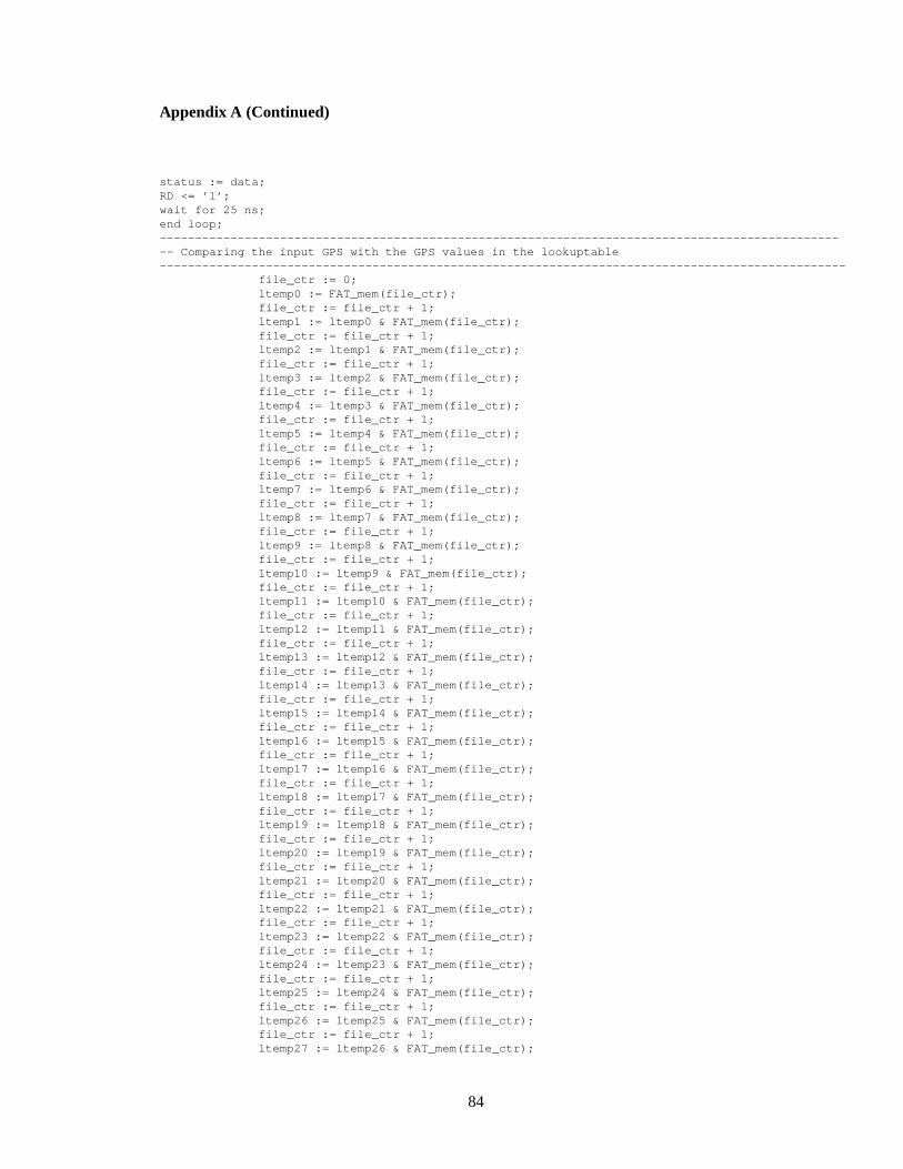
Appendix A (Continued)
status := data;RD <= ’1’;wait for 25 ns;end loop;-------------------------------------------------------------------------------------------------- Comparing the input GPS with the GPS values in the lookuptable-------------------------------------------------------------------------------------------------
file_ctr := 0;ltemp0 := FAT_mem(file_ctr);file_ctr := file_ctr + 1;ltemp1 := ltemp0 & FAT_mem(file_ctr);file_ctr := file_ctr + 1;ltemp2 := ltemp1 & FAT_mem(file_ctr);file_ctr := file_ctr + 1;ltemp3 := ltemp2 & FAT_mem(file_ctr);file_ctr := file_ctr + 1;ltemp4 := ltemp3 & FAT_mem(file_ctr);file_ctr := file_ctr + 1;ltemp5 := ltemp4 & FAT_mem(file_ctr);file_ctr := file_ctr + 1;ltemp6 := ltemp5 & FAT_mem(file_ctr);file_ctr := file_ctr + 1;ltemp7 := ltemp6 & FAT_mem(file_ctr);file_ctr := file_ctr + 1;ltemp8 := ltemp7 & FAT_mem(file_ctr);file_ctr := file_ctr + 1;ltemp9 := ltemp8 & FAT_mem(file_ctr);file_ctr := file_ctr + 1;ltemp10 := ltemp9 & FAT_mem(file_ctr);file_ctr := file_ctr + 1;ltemp11 := ltemp10 & FAT_mem(file_ctr);file_ctr := file_ctr + 1;ltemp12 := ltemp11 & FAT_mem(file_ctr);file_ctr := file_ctr + 1;ltemp13 := ltemp12 & FAT_mem(file_ctr);file_ctr := file_ctr + 1;ltemp14 := ltemp13 & FAT_mem(file_ctr);file_ctr := file_ctr + 1;ltemp15 := ltemp14 & FAT_mem(file_ctr);file_ctr := file_ctr + 1;ltemp16 := ltemp15 & FAT_mem(file_ctr);file_ctr := file_ctr + 1;ltemp17 := ltemp16 & FAT_mem(file_ctr);file_ctr := file_ctr + 1;ltemp18 := ltemp17 & FAT_mem(file_ctr);file_ctr := file_ctr + 1;ltemp19 := ltemp18 & FAT_mem(file_ctr);file_ctr := file_ctr + 1;ltemp20 := ltemp19 & FAT_mem(file_ctr);file_ctr := file_ctr + 1;ltemp21 := ltemp20 & FAT_mem(file_ctr);file_ctr := file_ctr + 1;ltemp22 := ltemp21 & FAT_mem(file_ctr);file_ctr := file_ctr + 1;ltemp23 := ltemp22 & FAT_mem(file_ctr);file_ctr := file_ctr + 1;ltemp24 := ltemp23 & FAT_mem(file_ctr);file_ctr := file_ctr + 1;ltemp25 := ltemp24 & FAT_mem(file_ctr);file_ctr := file_ctr + 1;ltemp26 := ltemp25 & FAT_mem(file_ctr);file_ctr := file_ctr + 1;ltemp27 := ltemp26 & FAT_mem(file_ctr);
84

Appendix A (Continued)
file_ctr := file_ctr + 1;ltemp28 := ltemp27 & FAT_mem(file_ctr);file_ctr := file_ctr + 1;ltemp29 := ltemp28 & FAT_mem(file_ctr);file_ctr := file_ctr + 1;ltemp30 := ltemp29 & FAT_mem(file_ctr);file_ctr := file_ctr + 1;ltemp31 := ltemp30 & FAT_mem(file_ctr);file1 := file_ctr;
if GPSlatlong = ltemp31 thenfile_ctr := file_ctr + 1;
file2 := file_ctr;ltemp0 := FAT_mem(file_ctr);
file_ctr := file_ctr + 1;ltemp1 := ltemp0 & FAT_mem(file_ctr);file_ctr := file_ctr + 1;
ltemp2 := ltemp1 & FAT_mem(file_ctr);file_ctr := file_ctr + 1;ltemp3 := ltemp2 & FAT_mem(file_ctr);
file_ctr := file_ctr + 1;ltemp4 := ltemp3 & FAT_mem(file_ctr);file_ctr := file_ctr + 1;
ltemp5 := ltemp4 & FAT_mem(file_ctr);lookupfilename := ltemp5(95 downto 8);
elsefile_ctr := file_ctr + 7;
file3 := file_ctr;ltemp0 := FAT_mem(file_ctr);
file_ctr := file_ctr + 1;ltemp1 := ltemp0 & FAT_mem(file_ctr);file_ctr := file_ctr + 1;
ltemp2 := ltemp1 & FAT_mem(file_ctr);file_ctr := file_ctr + 1;ltemp3 := ltemp2 & FAT_mem(file_ctr);file_ctr := file_ctr + 1;ltemp4 := ltemp3 & FAT_mem(file_ctr);file_ctr := file_ctr + 1;ltemp5 := ltemp4 & FAT_mem(file_ctr);file_ctr := file_ctr + 1;ltemp6 := ltemp5 & FAT_mem(file_ctr);file_ctr := file_ctr + 1;ltemp7 := ltemp6 & FAT_mem(file_ctr);file_ctr := file_ctr + 1;ltemp8 := ltemp7 & FAT_mem(file_ctr);file_ctr := file_ctr + 1;ltemp9 := ltemp8 & FAT_mem(file_ctr);file_ctr := file_ctr + 1;ltemp10 := ltemp9 & FAT_mem(file_ctr);file_ctr := file_ctr + 1;ltemp11 := ltemp10 & FAT_mem(file_ctr);file_ctr := file_ctr + 1;ltemp12 := ltemp11 & FAT_mem(file_ctr);file_ctr := file_ctr + 1;ltemp13 := ltemp12 & FAT_mem(file_ctr);file_ctr := file_ctr + 1;ltemp14 := ltemp13 & FAT_mem(file_ctr);file_ctr := file_ctr + 1;ltemp15 := ltemp14 & FAT_mem(file_ctr);file_ctr := file_ctr + 1;ltemp16 := ltemp15 & FAT_mem(file_ctr);file_ctr := file_ctr + 1;ltemp17 := ltemp16 & FAT_mem(file_ctr);
85
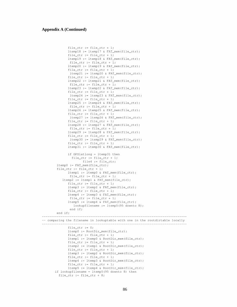
Appendix A (Continued)
file_ctr := file_ctr + 1;ltemp18 := ltemp17 & FAT_mem(file_ctr);file_ctr := file_ctr + 1;ltemp19 := ltemp18 & FAT_mem(file_ctr);file_ctr := file_ctr + 1;
ltemp20 := ltemp19 & FAT_mem(file_ctr);file_ctr := file_ctr + 1;ltemp21 := ltemp20 & FAT_mem(file_ctr);
file_ctr := file_ctr + 1;ltemp22 := ltemp21 & FAT_mem(file_ctr);file_ctr := file_ctr + 1;
ltemp23 := ltemp22 & FAT_mem(file_ctr);file_ctr := file_ctr + 1;ltemp24 := ltemp23 & FAT_mem(file_ctr);
file_ctr := file_ctr + 1;ltemp25 := ltemp24 & FAT_mem(file_ctr);file_ctr := file_ctr + 1;
ltemp26 := ltemp25 & FAT_mem(file_ctr);file_ctr := file_ctr + 1;ltemp27 := ltemp26 & FAT_mem(file_ctr);
file_ctr := file_ctr + 1;ltemp28 := ltemp27 & FAT_mem(file_ctr);file_ctr := file_ctr + 1;
ltemp29 := ltemp28 & FAT_mem(file_ctr);file_ctr := file_ctr + 1;ltemp30 := ltemp29 & FAT_mem(file_ctr);
file_ctr := file_ctr + 1;ltemp31 := ltemp30 & FAT_mem(file_ctr);
if GPSlatlong = ltemp31 thenfile_ctr := file_ctr + 1;
file4 := file_ctr;ltemp0 := FAT_mem(file_ctr);file_ctr := file_ctr + 1;
ltemp1 := ltemp0 & FAT_mem(file_ctr);file_ctr := file_ctr + 1;
ltemp2 := ltemp1 & FAT_mem(file_ctr);file_ctr := file_ctr + 1;ltemp3 := ltemp2 & FAT_mem(file_ctr);file_ctr := file_ctr + 1;ltemp4 := ltemp3 & FAT_mem(file_ctr);file_ctr := file_ctr + 1;
ltemp5 := ltemp4 & FAT_mem(file_ctr);lookupfilename := ltemp5(95 downto 8);
end if;end if;
-------------------------------------------------------------------------------- comparing the filename in lookuptable with one in the rootdirtable locally------------------------------------------------------------------------------
file_ctr := 0;ltemp0 := RootDir_mem(file_ctr);file_ctr := file_ctr + 1;ltemp1 := ltemp0 & RootDir_mem(file_ctr);file_ctr := file_ctr + 1;ltemp2 := ltemp1 & RootDir_mem(file_ctr);file_ctr := file_ctr + 1;ltemp3 := ltemp2 & RootDir_mem(file_ctr);file_ctr := file_ctr + 1;ltemp4 := ltemp3 & RootDir_mem(file_ctr);file_ctr := file_ctr + 1;ltemp5 := ltemp4 & RootDir_mem(file_ctr);
if lookupfilename = ltemp5(95 downto 8) thenfile_ctr := file_ctr + 8;
86

Appendix A (Continued)
tempfatentry := RootDir_mem(file_ctr);else
for i in 1 to maxrootdirentries loopfile_ctr := file_ctr + 13;ltemp0 := RootDir_mem(file_ctr);
file_ctr := file_ctr + 1;ltemp1 := ltemp0 & RootDir_mem(file_ctr);file_ctr := file_ctr + 1;ltemp2 := ltemp1 & RootDir_mem(file_ctr);file_ctr := file_ctr + 1;ltemp3 := ltemp2 & RootDir_mem(file_ctr);file_ctr := file_ctr + 1;ltemp4 := ltemp3 & RootDir_mem(file_ctr);file_ctr := file_ctr + 1;ltemp5 := ltemp4 & RootDir_mem(file_ctr);if lookupfilename = ltemp5(95 downto 8) then
file_ctr := file_ctr + 8;tempfatentry := RootDir_mem(file_ctr);
end if;exit when lookupfilename = ltemp5(95 downto 8);
end loop;end if;
incdatacylinderaddr := datacylinderaddr;incdataheadaddr := dataheadaddr;incdatasectoraddr := datasectoraddr;
----------------------------------------------------------------------------------------------- Reading all the entries of the first sector into a temporary FAT table---------------------------------------------------------------------------------------------incfatcylinderaddr := fatcylinderaddr;incfatheadaddr := fatheadaddr;incfatsectoraddr := fatsectoraddr;loopvar := "0000000010000000";--------------------------------------------------------------------------------- Storing the FAT Table locally----------------------------------------------------------------------------------------------------------------------------------------------------------Writing the cylinder low register in the flash-------------------------------------------------------------------------RD <= ’1’;WR <= ’1’;wait for 25 ns;Address <= "100";data <= incfatcylinderaddr;wait for 25 ns;WR <= ’0’;wait for 70 ns;WR <= ’1’;wait for 25 ns;data <= "ZZZZZZZZZZZZZZZZ";--------------------------------------------------------------------------------------Writing the cylinder high register in the flash-------------------------------------------------------------------------Address <= "101";data <= "0000000000000000";wait for 25 ns;WR <= ’0’;wait for 70 ns;WR <= ’1’;wait for 25 ns;data <= "ZZZZZZZZZZZZZZZZ";--------------------------------------------------------------------------------------Writing the head register in the flash-------------------------------------------------------------------------
87

Appendix A (Continued)
Address <= "110";data <= head_concat & incfatheadaddr;wait for 25 ns;WR <= ’0’;wait for 70 ns;WR <= ’1’;wait for 25 ns;data <= "ZZZZZZZZZZZZZZZZ";--------------------------------------------------------------------------------------Writing the sector count register in the flash-------------------------------------------------------------------------Address <= "010";data <= "0000000000000001";wait for 25 ns;
WR <= ’0’;wait for 70 ns;WR <= ’1’;wait for 25 ns;data <= "ZZZZZZZZZZZZZZZZ";--------------------------------------------------------------------------------------Writing the sector number register in the flash-------------------------------------------------------------------------Address <= "011";data <= incfatsectoraddr;wait for 25 ns;WR <= ’0’;wait for 70 ns;WR <= ’1’;wait for 25 ns;data <= "ZZZZZZZZZZZZZZZZ";--------------------------------------------------------------------------------------Writing the command register in the flash-------------------------------------------------------------------------Address <= "111";data <= cmd_addr;wait for 25 ns;
WR <= ’0’;wait for 70 ns;WR <= ’1’;wait for 25 ns;data <= "ZZZZZZZZZZZZZZZZ";--------------------------------------------------------------------------------------Reading the status register in the flash-------------------------------------------------------------------------RD <= ’0’;wait for 70 ns;status := data;RD <= ’1’;wait for 25 ns;while (status (7) /= ’0’) loopRD <= ’0’;wait for 70 ns;status := data;RD <= ’1’;wait for 25 ns;FAT_Ctr := 0;end loop;while (status(3) /= ’0’) loopAddress <= "000";wait for 25 ns;RD <= ’0’;wait for 70 ns;FAT_mem(FAT_Ctr) <= data;
88

Appendix A (Continued)
FAT_Ctr := FAT_Ctr + 1;RD <= ’1’;wait for 25 ns;Address <= "111";wait for 25 ns;RD <= ’0’;wait for 70 ns;status := data;RD <= ’1’;wait for 25 ns;end loop;while flag=1 loop
if tempfatentry > loopvar thenincfatsectoraddr := incfatsectoraddr + "0000000000000001";loopvar := loopvar + "0000000010000000";if incfatsectoraddr >= "0000000000010000" then
if incfatheadaddr < "0010" thenincfatheadaddr := incfatheadaddr + "0001";incfatsectoraddr := "0000000000000001";
elseincfatcylinderaddr := incdatacylinderaddr + "0000000000000001";incfatheadaddr := "0000";incfatsectoraddr := "0000000000000001";
end if;end if;
---------------------------------------------------------------------------Writing the cylinder low register in the flash------------------------------------------------------------------------RD <= ’1’;
WR <= ’1’;wait for 25 ns;
Address <= "100";data <= incfatcylinderaddr;wait for 25 ns;WR <= ’0’;wait for 70 ns;WR <= ’1’;wait for 25 ns;data <= "ZZZZZZZZZZZZZZZZ";--------------------------------------------------------------------------------------Writing the cylinder high register in the flash-------------------------------------------------------------------------Address <= "101";data <= "0000000000000000";wait for 25 ns;WR <= ’0’;wait for 70 ns;
WR <= ’1’;wait for 25 ns;data <= "ZZZZZZZZZZZZZZZZ";--------------------------------------------------------------------------------------Writing the head register in the flash-------------------------------------------------------------------------Address <= "110";data <= head_concat & incfatheadaddr;
wait for 25 ns;WR <= ’0’;wait for 70 ns;WR <= ’1’;wait for 25 ns;data <= "ZZZZZZZZZZZZZZZZ";
89

Appendix A (Continued)
--------------------------------------------------------------------------------------Writing the sector count register in the flash-------------------------------------------------------------------------Address <= "010";data <= "0000000000000001";wait for 25 ns;WR <= ’0’;wait for 70 ns;WR <= ’1’;wait for 25 ns;data <= "ZZZZZZZZZZZZZZZZ";--------------------------------------------------------------------------------------Writing the sector number register in the flash-------------------------------------------------------------------------Address <= "011";data <= incfatsectoraddr;wait for 25 ns;WR <= ’0’;wait for 70 ns;WR <= ’1’;wait for 25 ns;data <= "ZZZZZZZZZZZZZZZZ";--------------------------------------------------------------------------------------Writing the command register in the flash-------------------------------------------------------------------------Address <= "111";data <= cmd_addr;wait for 25 ns;WR <= ’0’;wait for 70 ns;WR <= ’1’;wait for 25 ns;data <= "ZZZZZZZZZZZZZZZZ";--------------------------------------------------------------------------------------Reading the status register in the flash-------------------------------------------------------------------------RD <= ’0’;wait for 70 ns;status := data;RD <= ’1’;wait for 25 ns;while (status (7) /= ’0’) loop
RD <= ’0’;wait for 70 ns;status := data;RD <= ’1’;wait for 25 ns;FAT_Ctr := 0;end loop;
while (status(3) /= ’0’) loopAddress <= "000";wait for 25 ns;RD <= ’0’;wait for 70 ns;FAT_mem(FAT_Ctr) <= data;FAT_Ctr := FAT_Ctr + 1;RD <= ’1’;wait for 25 ns;Address <= "111";wait for 25 ns;RD <= ’0’;wait for 70 ns;status := data;
90

Appendix A (Continued)
RD <= ’1’;wait for 25 ns;end loop;end if;
tempfatentrycopy := tempfatentry;incdatasectoraddr := tempfatentrycopy (7 downto 0) * sectorspercluster;incdatasectoroffset := incdatasectoraddr - "0000000000100000";
while incdatasectoroffset >= "0000000000100000" loopincdatasectoroffset := incdatasectoroffset - "0000000000100000";
end loop;
for j in 0 to 4 loopfor i in 0 to 14 loop
tempfatentrycopy(i) := tempfatentrycopy(i+1);end loop;
tempfatentrycopy(15):= ’0’;end loop;
if tempfatentrycopy < clustersperhead thenincdataheadaddr := tempfatentrycopy(3 downto 0);
elsewhile tempfatentrycopy > clustersperhead loopincdatacylinderaddr := incdatacylinderaddr + "0000000000000001";tempfatentrycopy := tempfatentrycopy - clustersperhead;
end loop;incdataheadaddr := tempfatentrycopy(3 downto 0);
end if;if incdatasectoraddr >= "0000000000100000" then
if incdataheadaddr < "0010" thenincdataheadaddr := incdataheadaddr + "0001";
incdatasectoraddr := incdatasectoroffset;else
incdatacylinderaddr := incdatacylinderaddr + "0000000000000001";incdataheadaddr := "0000";incdatasectoraddr := incdatasectoroffset;
end if;end if;
--------------------------------------------------------------------------------Playing out the next cluster from data area and finding the next cluster------------------------------------------------------------------------------for i in 1 to sectorspercluster loop--------------------------------------------------------------------------------------Writing the cylinder low register in the flash-------------------------------------------------------------------------RD <= ’1’;WR <= ’1’;wait for 25 ns;Address <= "100";data <= incdatacylinderaddr;wait for 25 ns;WR <= ’0’;wait for 70 ns;WR <= ’1’;wait for 25 ns;data <= "ZZZZZZZZZZZZZZZZ";--------------------------------------------------------------------------------------Writing the cylinder high register in the flash-------------------------------------------------------------------------Address <= "101";data <= "0000000000000000";wait for 25 ns;WR <= ’0’;wait for 70 ns;
91

Appendix A (Continued)
WR <= ’1’;wait for 25 ns;data <= "ZZZZZZZZZZZZZZZZ";--------------------------------------------------------------------------------------Writing the head register in the flash-------------------------------------------------------------------------Address <= "110";data <= head_concat & incdataheadaddr;wait for 25 ns;WR <= ’0’;wait for 70 ns;WR <= ’1’;wait for 25 ns;data <= "ZZZZZZZZZZZZZZZZ";--------------------------------------------------------------------------------------Writing the sector count register in the flash-------------------------------------------------------------------------Address <= "010";data <= "0000000000000001";wait for 25 ns;WR <= ’0’;wait for 70 ns;WR <= ’1’;wait for 25 ns;data <= "ZZZZZZZZZZZZZZZZ";--------------------------------------------------------------------------------------Writing the sector number register in the flash-------------------------------------------------------------------------Address <= "011";data <= incdatasectoraddr;wait for 25 ns;WR <= ’0’;wait for 70 ns;WR <= ’1’;wait for 25 ns;data <= "ZZZZZZZZZZZZZZZZ";--------------------------------------------------------------------------------------Writing the command register in the flash-------------------------------------------------------------------------Address <= "111";data <= cmd_addr;wait for 25 ns;WR <= ’0’;wait for 70 ns;WR <= ’1’;wait for 25 ns;data <= "ZZZZZZZZZZZZZZZZ";--------------------------------------------------------------------------------------Reading the status register in the flash-------------------------------------------------------------------------RD <= ’0’;wait for 70 ns;status := data;RD <= ’1’;wait for 25 ns;while (status (7) /= ’0’) loop
RD <= ’0’;wait for 70 ns;status := data;RD <= ’1’;wait for 25 ns;
end loop;while (status(3) /= ’0’) loop
92

Appendix A (Continued)
Address <= "000";wait for 25 ns;RD <= ’0’;wait for 70 ns;playdata := data;RD <= ’1’;wait for 25 ns;Address <= "111";wait for 25 ns;RD <= ’0’;wait for 70 ns;status := data;RD <= ’1’;
wait for 25 ns;playout := TO_BITVECTOR(playdata);
for j in 0 to 15 loopsdout <= playout(0);wait for 1 ns;playout := playout srl 1;
end loop;end loop;
incdatasectoraddr := incdatasectoraddr + "0000000000000001";if incdatasectoraddr >= "0000000001000000" then
if incdataheadaddr < "0010" thenincdataheadaddr := incdataheadaddr + "0001";
incdatasectoraddr := "0000000000000000";elseincdatacylinderaddr := incdatacylinderaddr + "0000000000000001";incdataheadaddr := "0000";incdatasectoraddr := "0000000000000000";
end if;end if;
end loop;incdatacylinderaddr := datacylinderaddr;incdataheadaddr := dataheadaddr;incdatasectoraddr := datasectoraddr;
------------------------------------------------------------------------------------------Finding the next tempfatentry from the FATtable ------------------------------------------------------------------------------------------tempfatvar := bits_to_int(tempfatentry);tempfatentry := FAT_mem(tempfatvar);exit when tempfatentry = "0000000011111111";
end loop;end process;end behavior;
93