High-Frequency Link Inverter Based on Multiple-Carrier PWM Philip T. Krein, Xin Geng, Robert Balog...
24
High-Frequency Link Inverter Based on Multiple- Carrier PWM Philip T. Krein, Xin Geng, Robert Balog University of Illinois March 2002
-
Upload
arron-spencer -
Category
Documents
-
view
223 -
download
0
Transcript of High-Frequency Link Inverter Based on Multiple-Carrier PWM Philip T. Krein, Xin Geng, Robert Balog...

High-Frequency Link Inverter Based on Multiple-Carrier PWM
Philip T. Krein, Xin Geng,Robert Balog
University of Illinois
March 2002
Outline
• The PWM cycloconverter.
• Dual-carrier PWM to build waveforms for HF links.
• Properties of dual-carrier signals for gate drives and other purposes.
• Experimental results.
• Conclusions.

The PWM Cycloconverter
• High-frequency (HF) link inverters can be constructed as:– A cascade of a high-frequency dc-dc converter and inverter.
– A “square-wave cycloconverter,” in which a high-frequency square-wave inverter provides the input to a cycloconverter.
HighFrequency
InverterInverter Load
HighFrequency
Inverter
Cyclo-Converter Load
(a) DC/DC converter type
(b) Cycloconverter type
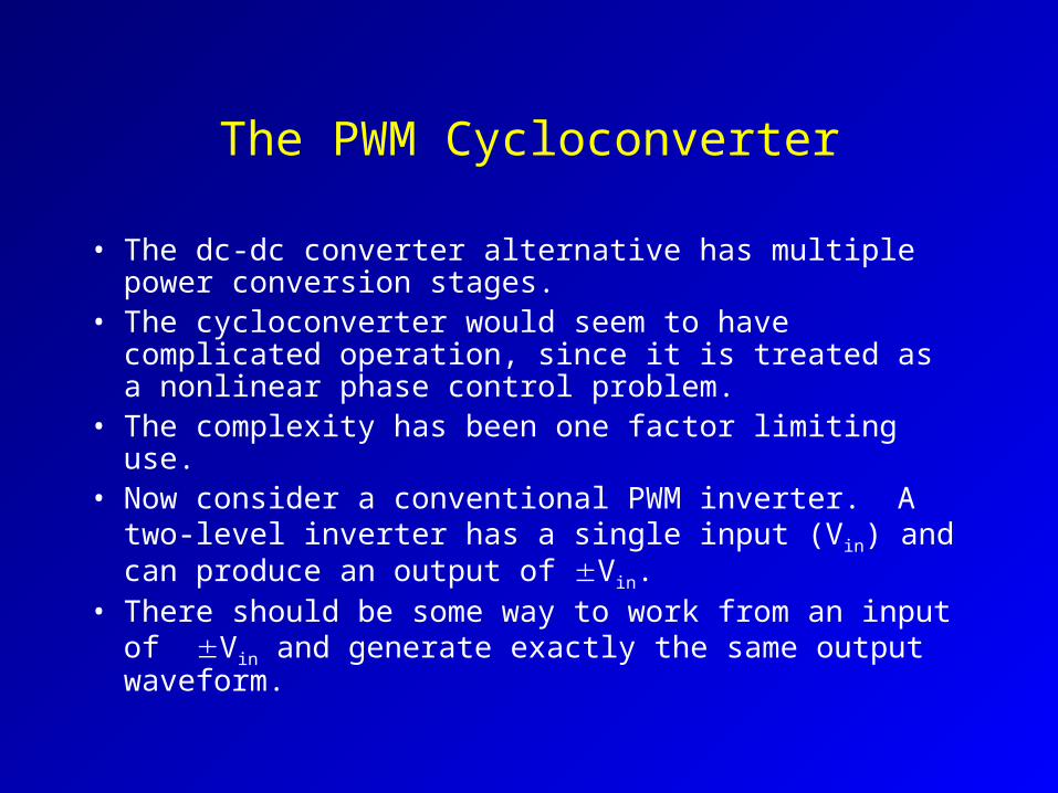
The PWM Cycloconverter
• The dc-dc converter alternative has multiple power conversion stages.
• The cycloconverter would seem to have complicated operation, since it is treated as a nonlinear phase control problem.
• The complexity has been one factor limiting use.• Now consider a conventional PWM inverter. A two-level
inverter has a single input (Vin) and can produce an output of Vin.
• There should be some way to work from an input of Vin and generate exactly the same output waveform.

The PWM Cycloconverter
• This is the PWM cycloconverter: use as input a simple square wave input at high frequency, then control the switches to produce an output that is exactly a conventional two-level PWM waveform.
• The PWM cycloconverter is not a new concept.
• What is new is that conventional PWM can be extended to cycloconverter operation with a multiple-carrier PWM process.

Dual-Carrier PWM
• Consider the use of two separate PWM waveforms, modulated with a desired low-frequency waveform m(t).
• This could be separate rising and falling ramps, triangles with phase shifts, or the like.
• Call these Carrier 1 and Carrier 2.• Now modulate both Carrier 1 and Carrier 2 with the signal
m(t), to give PWM 1 and PWM 2.• The sum PWM 1 + PWM 2 has low-frequency content
2m(t).• The difference PWM 1 – PWM 2 has no low-frequency
content.

Dual-Carrier PWM
• Is the result trivial? Not if we use time multiplexing to make sure the final waveform retains switching behavior.
• Several choices of combinations are available.
ca rrie r
m odu la tingfunction
P1
P2
+ /-
gate dr iv e s equenc e
H F lin kvo ltag e inpu t Sw itc hing
Control
c y c loc onv erterv oltage output
C1(t)
C2(t)
M1(t)
M2(t)
0/180o Phas eShif ter 1
Comparator
Comparator
Dec ommutator
0/180o Phas eShif ter 3
0/180o Phas eShif ter 2
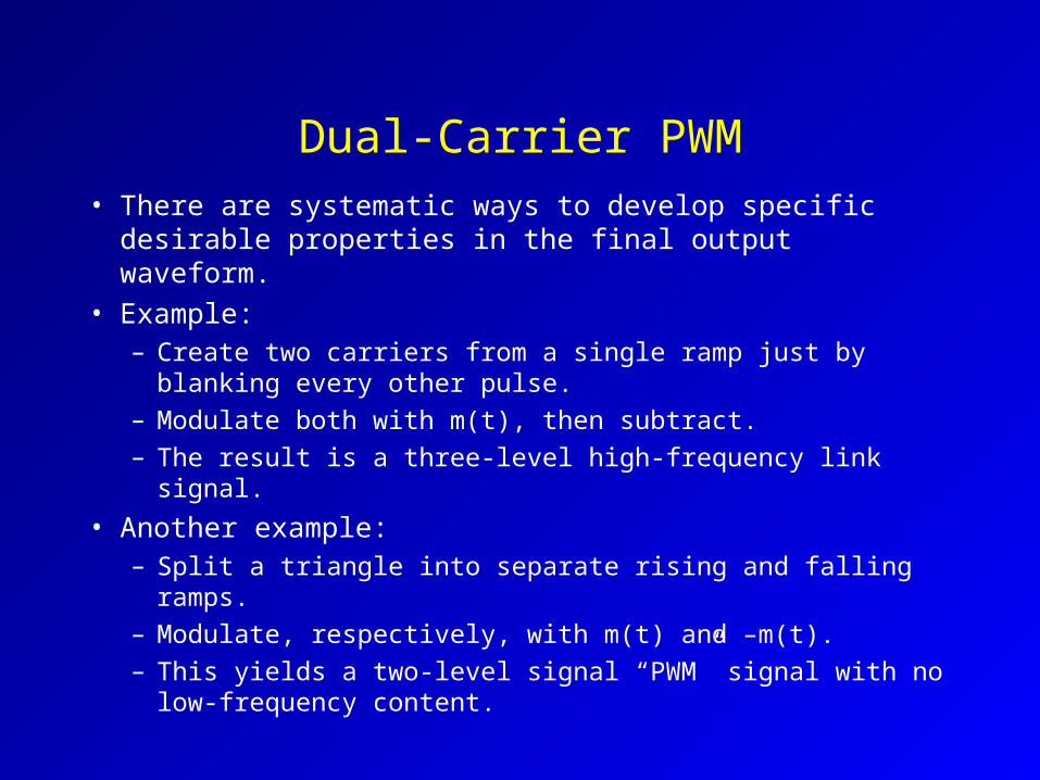
Dual-Carrier PWM
• There are systematic ways to develop specific desirable properties in the final output waveform.
• Example: – Create two carriers from a single ramp just by blanking
every other pulse.
– Modulate both with m(t), then subtract.
– The result is a three-level high-frequency link signal.
• Another example:– Split a triangle into separate rising and falling ramps.
– Modulate, respectively, with m(t) and –m(t).
– This yields a two-level signal “PWM” signal with no low-frequency content.
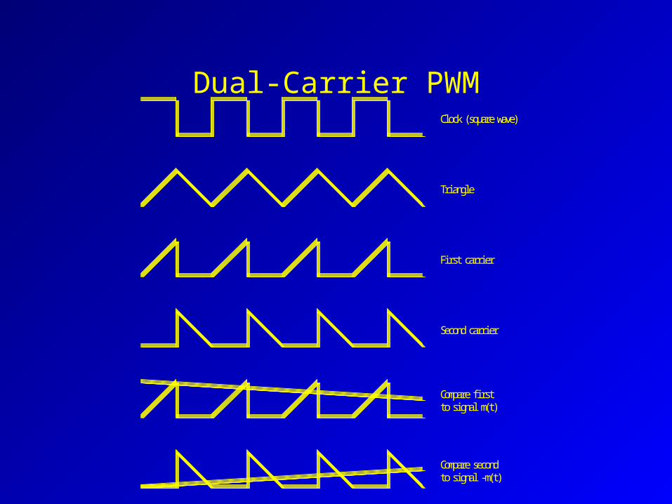
Dual-Carrier PWMClock (square wave)
Triangle
First carrier
Second carrier
Compare firstto signal m(t)
Compare secondto signal -m(t)

Dual-Carrier PWM
• The PWM sum has 50% duty, but retains the information.
Compare firstto signal m(t)
Compare secondto signal -m(t)
The original clock
Use one comparator toset, the other to reset.This is two-carrier PWM(t).

Dual-Carrier PWM
• What about the desired two-level PWM output?
• Use the square wave clock as the input to a cycloconverter.
• Use the sum waveform PWM(t) as the gate control.
• This “convolution” process of clock and PWM(t) recovers the desired two-level PWM output.
The original clock
Use one comparator toset, the other to reset.This is two-carrier PWM(t).
Clock convolved with PWM(t).This is conventional PWM, witheach turn-off advanced relativeto the clock.

Dual-Carrier PWM
• The PWM waveform is this example is also always phase-advanced with respect to the original square wave.
• List the combinations for two-carrier PWM.
TABLE 1. COMBINATION CONDITONS (WITH DECOMMUTATOR) AND RESULTING TWO-CARRIER PWM SEQUENCES
Carrier Type
Phase Shifter 1
Phase Shifter 2
Phase Shifter 3
Combining Method
Gate Drive Signal Type
Output PWM Equivalent
1 Triangle 0 0 180º Add 2-Level Ramp PWM at double fswitch
2 Triangle 0 180º 0 Add 2-Level Ramp PWM at double fswitch
3 Triangle 0 0 0 Subtract 3-Level Triangle PWM
4 Triangle 180º 0 180º Add 2-Level Ramp PWM at double fswitch
5 Triangle 180º 180º 0 Add 2-Level Ramp PWM at double fswitch
6 Triangle 180º 0 0 Subtract 3-Level Triangle PWM
7 Ramp 0 0 180º Add 2-Level Triangle PWM
8 Ramp 0 180º 0 Add 2-Level Triangle PWM
9 Ramp 0 0 0 Subtract 3-Level Ramp PWM at double fswitch
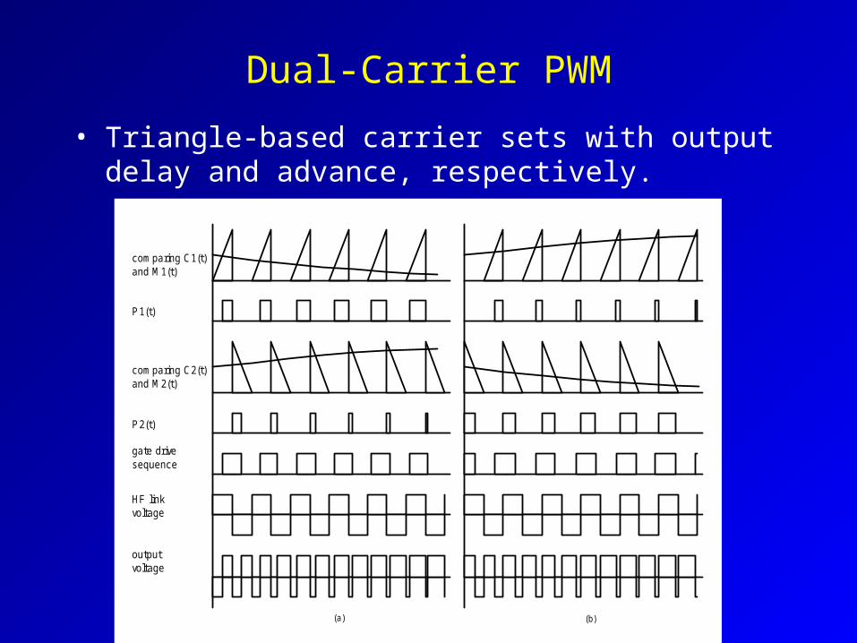
Dual-Carrier PWM
• Triangle-based carrier sets with output delay and advance, respectively.
comparing C1(t)and M1(t)
comparing C2(t)and M2(t)
P1(t)
P2(t)
gate drivesequence
HF linkvoltage
outputvoltage
(a) (b)
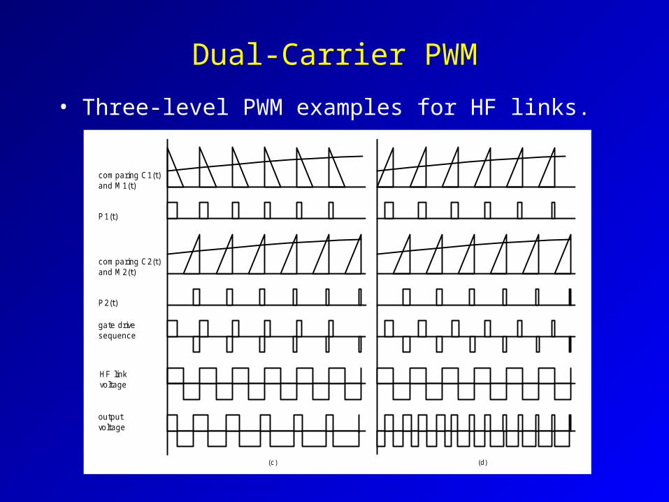
Dual-Carrier PWM
• Three-level PWM examples for HF links.
com paring C1(t)and M 1(t)
com paring C2(t)and M 2(t)
P 1(t)
P 2(t)
gate drivesequence
HF linkvoltage
outputvoltage
(c ) (d)

Properties in the Two-Carrier Case
• We can select among several properties:– By using carriers that alternately control turn-on and turn-
off, gate waveforms with 50% duty can be generated.
– The combined signal can have pure advance or delay.
– The resulting PWM output can be generated with an effectively doubled switching frequency.

Properties in the Two-Carrier Case
1. The two-carrier process allows conventional PWM modulators, combined with some simple logic, to generate waveforms for PWM cycloconverters.
2. With use of both advanced and delayed gating waveforms, natural commutation can be supported, in a manner equivalent to conventional sine wave SCR cycloconverters.
3. The cases that yield 50% duty ratio gating signals are especially valuable for transformer gate drives.

Experimental Results
• The two-carrier technique has been used to build a simple “naturally commutated PWM cycloconverter.”
• This represents a high-frequency link inverter that makes use of conventional PWM to provide control – with no intermediate dc-dc converter.
• SCRs are used – only the leading edge of the combined two-carrier signal is needed for the gate drives. (IGBTs could have been used instead.)
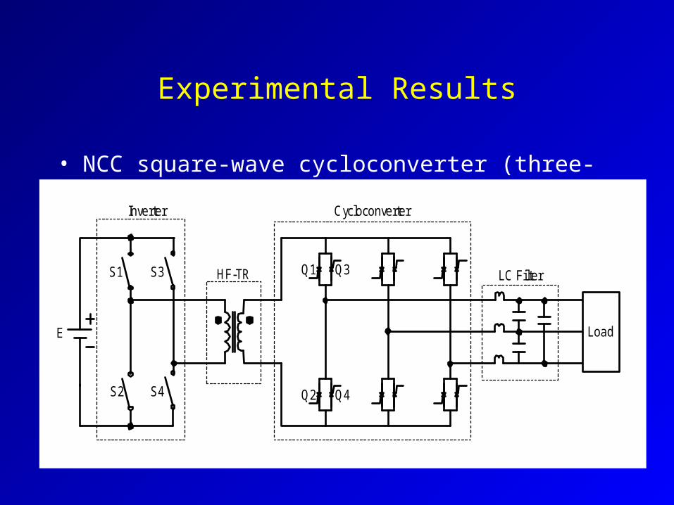
Experimental Results
• NCC square-wave cycloconverter (three-phase).
S1
S4S2
S3 HF-TR Q1
Q4
Q3
Q2
Inverter Cycloconverter
LC Filter
LoadE
Experimental Results
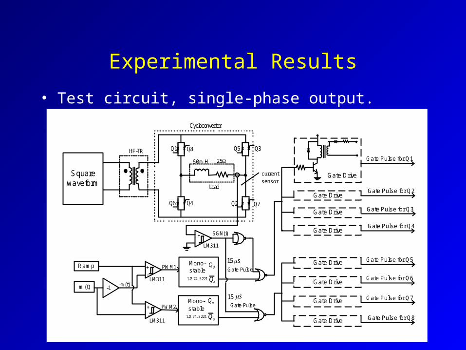
• Test circuit, single-phase output.
HF-TR Q1
Q4
Q3Q5
Cycloconverter
Load
Squarewaveform
60m H
Ram p
m (t) -1-m(t)
+-
PWM2
PWM1 Gate Pulse
Gate Pulse
currentsensor
+-
+-
25
Q8
Q7Q6 Q2
Mono-s table
1/2 74LS221
aQ
Mono-s table
1/2 74LS221dQ
dQ
SGN(i)
LM311
LM311
Gate Drive
Gate Drive
Gate Drive
Gate Drive
Gate Drive
Gate Drive
Gate Drive
Gate Drive
s15
s
Gate Pulse for Q1
Gate Pulse for Q2
Gate Pulse for Q3
Gate Pulse for Q4
Gate Pulse for Q5
Gate Pulse for Q6
Gate Pulse for Q7
Gate Pulse for Q8
LM311
15
Q a

Experimental Results
• The modulation process.
• Only the leading edges are needed.
Experimental Results
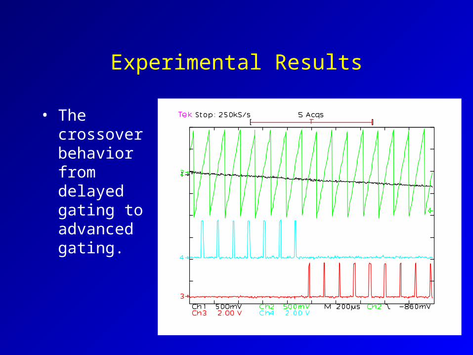
• The crossover behavior from delayed gating to advanced gating.
Experimental Results
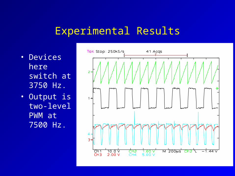
• Devices here switch at 3750 Hz.
• Output is two-level PWM at 7500 Hz.

Conclusion
• A multiple-carrier method can be used to generate PWM gating signals with a variety of properties.
• Two-carrier signals chosen to cancel the baseband signal m(t) support high-frequency link inverters.
• These inverters, PWM cycloconverters, eliminate a power stage but produce conventional PWM output waveforms.
• The control complexity is similar to familiar PWM, but with multiple signal paths.
Conclusion
• The multiple-signal output can be tailored for useful properties, such as gate drives with 50% duty ratio under all modulating signals, and outputs that provide an effective doubling of the switching frequency.