High Feature Digital Audio Processor with SRC · AK7601A is a high feature audio processor with...
63
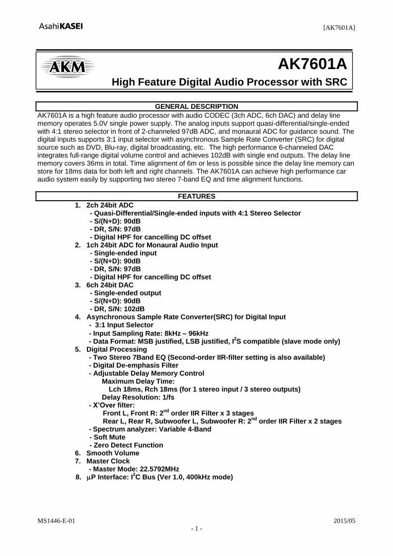
[AK7601A] MS1446-E-01 2015/05 - 1 - GENERAL DESCRIPTION AK7601A is a high feature audio processor with audio CODEC (3ch ADC, 6ch DAC) and delay line memory operates 5.0V single power supply. The analog inputs support quasi-differential/single-ended with 4:1 stereo selector in front of 2-channeled 97dB ADC, and monaural ADC for guidance sound. The digital inputs supports 3:1 input selector with asynchronous Sample Rate Converter (SRC) for digital source such as DVD, Blu-ray, digital broadcasting, etc. The high performance 6-channeled DAC integrates full-range digital volume control and achieves 102dB with single end outputs. The delay line memory covers 36ms in total. Time alignment of 6m or less is possible since the delay line memory can store for 18ms data for both left and right channels. The AK7601A can achieve high performance car audio system easily by supporting two stereo 7-band EQ and time alignment functions. FEATURES 1. 2ch 24bit ADC - Quasi-Differential/Single-ended inputs with 4:1 Stereo Selector - S/(N+D): 90dB - DR, S/N: 97dB - Digital HPF for cancelling DC offset 2. 1ch 24bit ADC for Monaural Audio Input - Single-ended input - S/(N+D): 90dB - DR, S/N: 97dB - Digital HPF for cancelling DC offset 3. 6ch 24bit DAC - Single-ended output - S/(N+D): 90dB - DR, S/N: 102dB 4. Asynchronous Sample Rate Converter(SRC) for Digital Input - 3:1 Input Selector - Input Sampling Rate: 8kHz 96kHz - Data Format: MSB justified, LSB justified, I 2 S compatible (slave mode only) 5. Digital Processing - Two Stereo 7Band EQ (Second-order IIR-filter setting is also available) - Digital De-emphasis Filter - Adjustable Delay Memory Control Maximum Delay Time: Lch 18ms, Rch 18ms (for 1 stereo input / 3 stereo outputs) Delay Resolution: 1/fs - X’Over filter: Front L, Front R: 2 nd order IIR Filter x 3 stages Rear L, Rear R, Subwoofer L, Subwoofer R: 2 nd order IIR Filter x 2 stages - Spectrum analyzer: Variable 4-Band - Soft Mute - Zero Detect Function 6. Smooth Volume 7. Master Clock - Master Mode: 22.5792MHz 8. P Interface: I 2 C Bus (Ver 1.0, 400kHz mode) High Feature Digital Audio Processor with SRC AK7601A
Transcript of High Feature Digital Audio Processor with SRC · AK7601A is a high feature audio processor with...
[AK7601A]
MS1446-E-01 2015/05
- 1 -
GENERAL DESCRIPTION
AK7601A is a high feature audio processor with audio CODEC (3ch ADC, 6ch DAC) and delay line memory operates 5.0V single power supply. The analog inputs support quasi-differential/single-ended with 4:1 stereo selector in front of 2-channeled 97dB ADC, and monaural ADC for guidance sound. The digital inputs supports 3:1 input selector with asynchronous Sample Rate Converter (SRC) for digital source such as DVD, Blu-ray, digital broadcasting, etc. The high performance 6-channeled DAC integrates full-range digital volume control and achieves 102dB with single end outputs. The delay line memory covers 36ms in total. Time alignment of 6m or less is possible since the delay line memory can store for 18ms data for both left and right channels. The AK7601A can achieve high performance car audio system easily by supporting two stereo 7-band EQ and time alignment functions.
FEATURES
1. 2ch 24bit ADC - Quasi-Differential/Single-ended inputs with 4:1 Stereo Selector - S/(N+D): 90dB - DR, S/N: 97dB - Digital HPF for cancelling DC offset
2. 1ch 24bit ADC for Monaural Audio Input - Single-ended input - S/(N+D): 90dB - DR, S/N: 97dB - Digital HPF for cancelling DC offset
3. 6ch 24bit DAC - Single-ended output - S/(N+D): 90dB - DR, S/N: 102dB
4. Asynchronous Sample Rate Converter(SRC) for Digital Input - 3:1 Input Selector
- Input Sampling Rate: 8kHz 96kHz - Data Format: MSB justified, LSB justified, I
2S compatible (slave mode only)
5. Digital Processing - Two Stereo 7Band EQ (Second-order IIR-filter setting is also available) - Digital De-emphasis Filter - Adjustable Delay Memory Control
Maximum Delay Time: Lch 18ms, Rch 18ms (for 1 stereo input / 3 stereo outputs)
Delay Resolution: 1/fs - X’Over filter:
Front L, Front R: 2nd
order IIR Filter x 3 stages Rear L, Rear R, Subwoofer L, Subwoofer R: 2
nd order IIR Filter x 2 stages
- Spectrum analyzer: Variable 4-Band - Soft Mute - Zero Detect Function
6. Smooth Volume 7. Master Clock
- Master Mode: 22.5792MHz 8. P Interface: I
2C Bus (Ver 1.0, 400kHz mode)
High Feature Digital Audio Processor with SRC
AK7601A

[AK7601A]
MS1446-E-01 2015/05
- 2 -
9. Power Supply
- Analog: AVDD = 4.5 5.5V
- Digital: DVDD = 3.0 5.5V 10. Power Consumption: 80mA
11. Ta = - 40 85°C 12. Package: 48LQFP(0.5mm pitch)
Block Diagram
2ch A
DC
14B
and E
Q
(2nd IIR
x 1
4)
Dela
y
Contr
ol
AOUT1L
O AOUT1R
AOUT2L
AOUT2R
AOUT3L
AOUT3R
SCL
XTI
XTO
PDN
DVDD AVDD VSS1 VSS2 VSS4
DZF
4Band Spectrum
Analyser Filter
(2nd
IIR x 1stIIR) x 4
IBICK1
1 IBICK2
MONOIN
2ch
DA
C
D-V
ol
D-V
ol
D-V
ol
IBICK3
ILRCK1
1 ILRCK2
ILRCK3
SDTI1
1 SDTI2
SDTI3
AINL4
AINL1
GNDIN1
AINR1
AINL2
GNDIN2
AINR4
AINR2
AINL3
AINR3
SDA D
-Vol
1ch A
DC
2ch S
RC
I2C
Interface
X’tal
Oscillator
VCOM VREFH REF18 VSS3
MCKO
MUTEN
2ch
DA
C
2ch
DA
C
SDTO1/SDTO3 SDTO2/SDTI4
OBICK
OLRCK
CLKMODE
2nd
IIR x 3
x2ch
2nd
IIR x 2
x2ch
2nd
IIR x 2
x2ch
Sw
itch
Switch
Functio
n
Figure 1. Block Diagram

[AK7601A]
MS1446-E-01 2015/05
- 3 -
Ordering Guide
AK7601AVQ -40 +85C 48pin LQFP(0.5mm pitch)
AKD7601A Evaluation board for AK7601A
Pin Layout
VSS3
XT
O
38
CLKMODE
36
39
REF18 40
VSS4 41
MONOIN
42
AINL1 43
GNDIN1 44
AINR1 45
AINL2 46
GNDIN2 47
AINR2 48
XT
I 35
ILR
CK
1
34
ILR
CK
2
33
ILR
CK
3
32
IBIC
K1
31
IBIC
K2
30
IBIC
K3
29
SD
TI1
28
SD
TI2
27
SD
TI3
26
AIN
L3
1
AIN
R3
2
AIN
L4
3
AIN
R4
4
VC
OM
5
AV
DD
6
VS
S1
7
8
AO
UT
1L
9
AO
UT
1R
10
AO
UT
2L
11
23
22
21
20
19
18
17
16
15
14
13
SDTO1/SDTO3
SDTO2/SDTI4
OLRCK
OBICK
MCKO
SCL
SDA
PDN
DZF
AOUT3R
AOUT3L
AK7601AVQ
Top View
AO
UT
2R
12
24 VSS2
DV
DD
25
MUTEN 37
VR
EF
H
Figure 2. Pin Layout
[AK7601A]
MS1446-E-01 2015/05
- 4 -
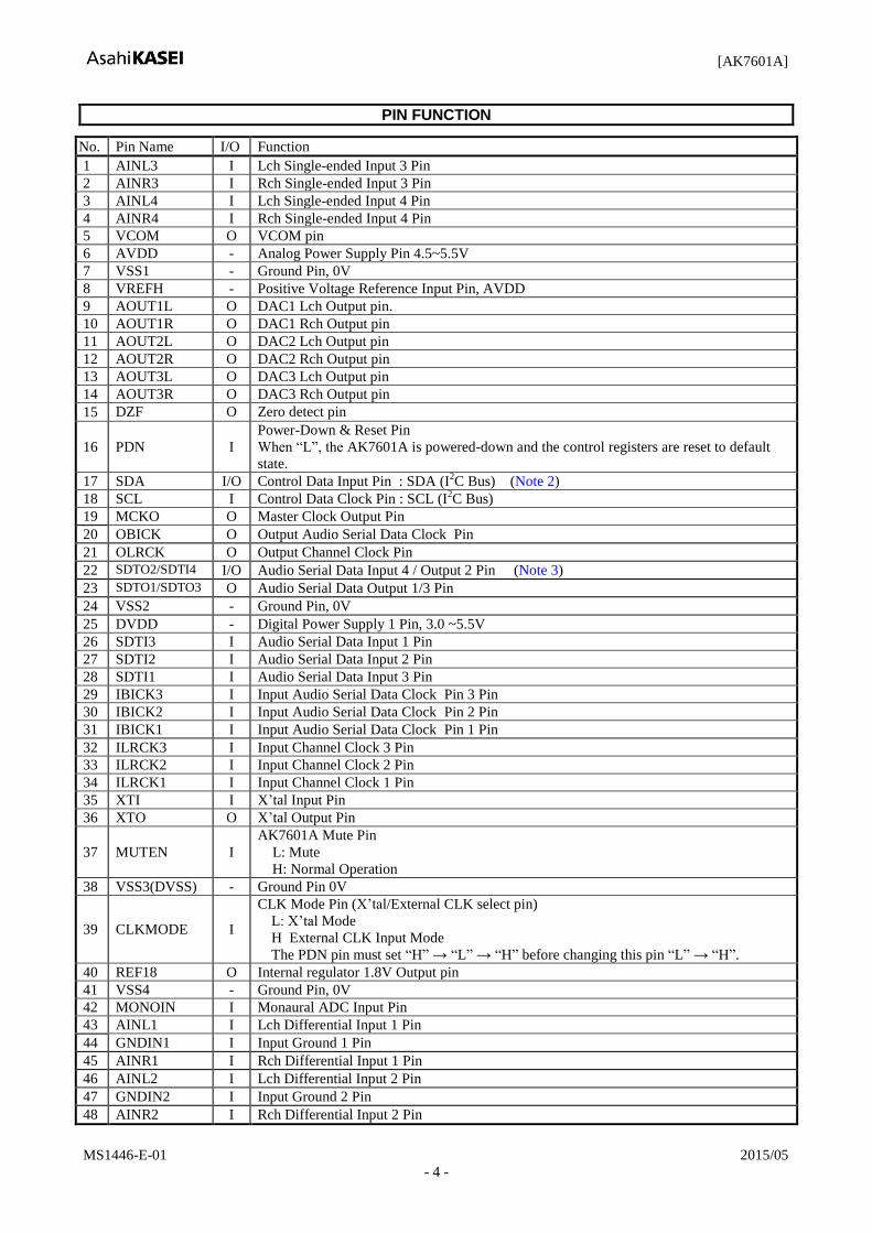
PIN FUNCTION
No. Pin Name I/O Function
1 AINL3 I Lch Single-ended Input 3 Pin
2 AINR3 I Rch Single-ended Input 3 Pin
3 AINL4 I Lch Single-ended Input 4 Pin
4 AINR4 I Rch Single-ended Input 4 Pin
5 VCOM O VCOM pin
6 AVDD - Analog Power Supply Pin 4.5~5.5V
7 VSS1 - Ground Pin, 0V
8 VREFH - Positive Voltage Reference Input Pin, AVDD
9 AOUT1L O DAC1 Lch Output pin.
10 AOUT1R O DAC1 Rch Output pin
11 AOUT2L O DAC2 Lch Output pin
12 AOUT2R O DAC2 Rch Output pin
13 AOUT3L O DAC3 Lch Output pin
14 AOUT3R O DAC3 Rch Output pin
15 DZF O Zero detect pin
16 PDN I
Power-Down & Reset Pin
When “L”, the AK7601A is powered-down and the control registers are reset to default
state.
17 SDA I/O Control Data Input Pin : SDA (I2C Bus) (Note 2)
18 SCL I Control Data Clock Pin : SCL (I2C Bus)
19 MCKO O Master Clock Output Pin
20 OBICK O Output Audio Serial Data Clock Pin
21 OLRCK O Output Channel Clock Pin
22 SDTO2/SDTI4 I/O Audio Serial Data Input 4 / Output 2 Pin (Note 3)
23 SDTO1/SDTO3 O Audio Serial Data Output 1/3 Pin
24 VSS2 - Ground Pin, 0V
25 DVDD - Digital Power Supply 1 Pin, 3.0 ~5.5V
26 SDTI3 I Audio Serial Data Input 1 Pin
27 SDTI2 I Audio Serial Data Input 2 Pin
28 SDTI1 I Audio Serial Data Input 3 Pin
29 IBICK3 I Input Audio Serial Data Clock Pin 3 Pin
30 IBICK2 I Input Audio Serial Data Clock Pin 2 Pin
31 IBICK1 I Input Audio Serial Data Clock Pin 1 Pin
32 ILRCK3 I Input Channel Clock 3 Pin
33 ILRCK2 I Input Channel Clock 2 Pin
34 ILRCK1 I Input Channel Clock 1 Pin
35 XTI I X’tal Input Pin
36 XTO O X’tal Output Pin
37 MUTEN I
AK7601A Mute Pin
L: Mute
H: Normal Operation
38 VSS3(DVSS) - Ground Pin 0V
39 CLKMODE I
CLK Mode Pin (X’tal/External CLK select pin)
L: X’tal Mode
H External CLK Input Mode
The PDN pin must set “H” → “L” → “H” before changing this pin “L” → “H”.
40 REF18 O Internal regulator 1.8V Output pin
41 VSS4 - Ground Pin, 0V
42 MONOIN I Monaural ADC Input Pin
43 AINL1 I Lch Differential Input 1 Pin
44 GNDIN1 I Input Ground 1 Pin
45 AINR1 I Rch Differential Input 1 Pin
46 AINL2 I Lch Differential Input 2 Pin
47 GNDIN2 I Input Ground 2 Pin
48 AINR2 I Rch Differential Input 2 Pin

[AK7601A]
MS1446-E-01 2015/05
- 5 -
Note 1. All digital input pins must not be allowed to float.
Note 2. Input pin when powered-down.
Note 3. Output pin when powered-down
Handling of Unused Pin The unused I/O pins should be processed appropriately as below
Classification Pin Name Setting
Analog
AINL1, GNDIN1, AINR1, AINL2, GNDIN2, AINR2,
AINL3, AINR3, AINL4, AINR4, MONOIN Open
AOUT1L, AOUT1R, AOUT2L, AOUT2R, AOUT3L,
AOUT3R Open
Digital
IBICK1, IBICK2, IBICK3, ILRCK1, ILRCK2,
ILRCK3, SDTI1, SDTI2, SDTI3, SDTI4 Connect to VSS2
OBICK, OLRCK, MCKO, SDTO1/SDTO3, SDTO2,
XTO Open

[AK7601A]
MS1446-E-01 2015/05
- 6 -
ABSOLUTE MAXMUM RATING
(VSS1=VSS2=VSS3=VSS4=0V; Note 4)
Parameter Symbol min max Unit
Power Supplies Analog
Digital
AVDD
DVDD
-0.3
-0.3
6.0
6.0
V
V
Input Current (any pins except for supplies) IIN - 10 mA
Analog Input Voltage (Note 5) VINA -0.3 AVDD+0.3 V
Digital Input Voltage (Note 6) VIND -0.3 DVDD+0.3 V
Ambient Temperature (power applied) Ta -40 85 C
Storage Temperature Tstg -65 150 C
Note 4. All indicated voltages are with respect to ground VSS1, VSS2, VSS3 and VSS4 must be connected to the analog
ground plane.
Note 5. Analog input pins are AINL1-4, AINR1-4, GNDIN1-2 and MONOIN.
Note 6. Digital input pins are SDTI1-4, ILRCK1-3, IBICK1-3, MUTEN, SDA, and SCL.
WARNING: Operating at or beyond these limits may result in permanent damage to the device. Normal operation is not
guaranteed at these critical conditions.
RECOMMENDED OPERATING CONDITIONS
(VSS1=VSS2=VSS3=VSS4 =0V; Note 4)
Parameter Symbol min typ max Unit
Power Supplies
(Note 7)
Analog
Digital
AVDD
DVDD
4.5
3.0
5.0
5.0
5.5
AVDD
V
V
Note 7. AVDD must be supplied after DVDD is ON. The PDN pin must be “L” until all power supplies are ON, then put
the PDN pin to “H”. All power supplies of the AK7601A are must be ON. Do not turn any power supply off
(means the same voltage as ground or floating) independently. When using the AK7601A with I²C bus, the
power supply of the AK7601A must not be turned off unless the power supplies of the surrounding device are
turned off.
* AKM assumes no responsibility for the usage beyond the conditions in this datasheet.

[AK7601A]
MS1446-E-01 2015/05
- 7 -
ANALOG CHARACTERISTICS
(Ta=25C; AVDD=5.0V, DVDD =5.0V; VSS1=VSS2=VSS3=VSS4=0V; VREFH=AVDD, fs=44.1kHz; Signal
Frequency=1kHz; 24bit Data; Measurement Frequency=20Hz20kHz at; unless otherwise specified)
Parameter min typ max Unit
ADC Analog Input Characteristics (Pseudo differential inputs)
Resolution 24 Bits
S/(N+D) BW=20kHz -1dBFS 83 90 dB
-60dBFS 35
DR (-60dBFS with A-weighted) 90 97 dB
S/N (A-weighted) 90 97 dB
Interchannel Isolation 90 110 dB
Interchannel Gain Mismatch 0 0.5 dB
Gain Drift 20 - ppm/C
Input Voltage AIN=0.65xVREFH 3.09 3.25 3.41 Vpp
Input Resistance AINL1, AINR1, AINL2, AINR2 22 45 k
GNDIN1, GNDIN2 22 90 k
Power Supply Rejection (Note 8) 55 dB
Common Mode Rejection Ratio (CMRR) (Note 9) 40 dB
ADC Analog Input Characteristics (Single-ended inputs)
Resolution 24 Bits
S/(N+D) BW=20kHz -1dBFS 83 90 dB
-60dBFS 35
DR (-60dBFS with A-weighted) 90 97 dB
S/N (A-weighted) 90 97 dB
Interchannel Isolation 90 110 dB
Interchannel Gain Mismatch 0 0.5 dB
Gain Drift 20 - ppm/C
Input Voltage AIN=0.65xVREFH 3.09 3.25 3.41 Vpp
Input Resistance (AINL3, AINR3, AINL4, AINR4) 22 45 k
Power Supply Rejection (Note 8) 55 dB
ADC Analog Input Characteristics (Monaural input)
Resolution 24 Bits
S/(N+D) BW=20kHz -1dBFS 83 90 dB
-60dBFS 35
DR (-60dBFS with A-weighted) 90 97 dB
S/N (A-weighted) 90 97 dB
Gain Drift 20 - ppm/C
Input Voltage AIN=0.65xVREFH 3.09 3.25 3.41 Vpp
Input Resistance 22 45 k
Power Supply Rejection (Note 8) 55 dB
DAC Analog Output Characteristics (single outputs)
Resolution 24 Bits
S/(N+D) BW=20kHz 0dBFS 83 90 dB
-60dBFS 39
DR (-60dBFS with A-weighted) 93 102 dB
S/N (A-weighted) 93 102 dB
Interchannel Isolation 90 110 dB
Interchannel Gain Mismatch 0 0.5 dB
Gain Drift 20 - ppm/C
Output Voltage AOUT=0.65xVREFH 3.09 3.25 3.41 Vpp
Load Resistance (AC Load) 5 k
Load Capacitance 30 pF
Power Supply Rejection (Note 8) 55 dB

[AK7601A]
MS1446-E-01 2015/05
- 8 -
ADC to DAC Characteristics (single outputs)
Resolution 24 Bits
S/(N+D) BW=20kHz -1dBFS 80 87 dB
-60dBFS 34
DR (-60dBFS with A-weighted) 87 96 dB
S/N (A-weighted) 87 96 dB
Note 8. PSR is applied to AVDD and DVDD with 1kHz, 50mVpp. This is the value of convoluted sinusoidal voltage of
1kHz and 50mVpp when the VREFH pin is held +5V.
Note 9. This is a value when the frequency range is 20Hz ~ 20kHz assuming an external capacitor is 10uF±30% and
GDNIN1/2 amplitude is 100mVpp.
SRC CHARACTERISTICS
(Ta=25C; AVDD=5.0V, DVDD =5.0V; VSS1=VSS2=VSS3=VSS4=0V; VREFH=AVDD, fs=44.1kHz; Signal
Frequency=1kHz; 24bit Data; Measurement Frequency=20Hz20kHz; unless otherwise specified)
Parameter Symbol min typ max Unit
SRC Characteristics:
Resolution 24 Bits
Input Sample Rate FSI 8 96 kHz
Output Sample Rate FSO 44.1 kHz
THD+N (Input = 1kHz, 0dBFS, Note 10) FSI =48kHz -130 -100 dB
Dynamic Range (Input = 1kHz, 60dBFS, Note 10)
FSI = 48kHz
Dynamic Range (Input = 1kHz, -60dBFS, A-weighted, Note 10)
FSI = 48kHz
136
140
120
dB
dB
Ratio between Input and Output Sample Rate FSO/FSI 44.1/96 44.1/8 -
Note 10. Measured by Audio Precision System Two Cascade.
Parameter min typ max Unit
Power Supplies
Power Supply Current
Normal Operation (PDN pin = “H”)
AVDD
DVDD
Power-down mode (PDN pin = “L”)
AVDD+DVDD (Note 12)
54
11
10
73
15
100
mA
mA
µA
Note 11. Power supply current values are for when ADC, DAC and SRC are in operation.
Note 12. When the AK7601A is not in operation. All digital input pins including clock pins are held to VSS2.
[AK7601A]
MS1446-E-01 2015/05
- 9 -
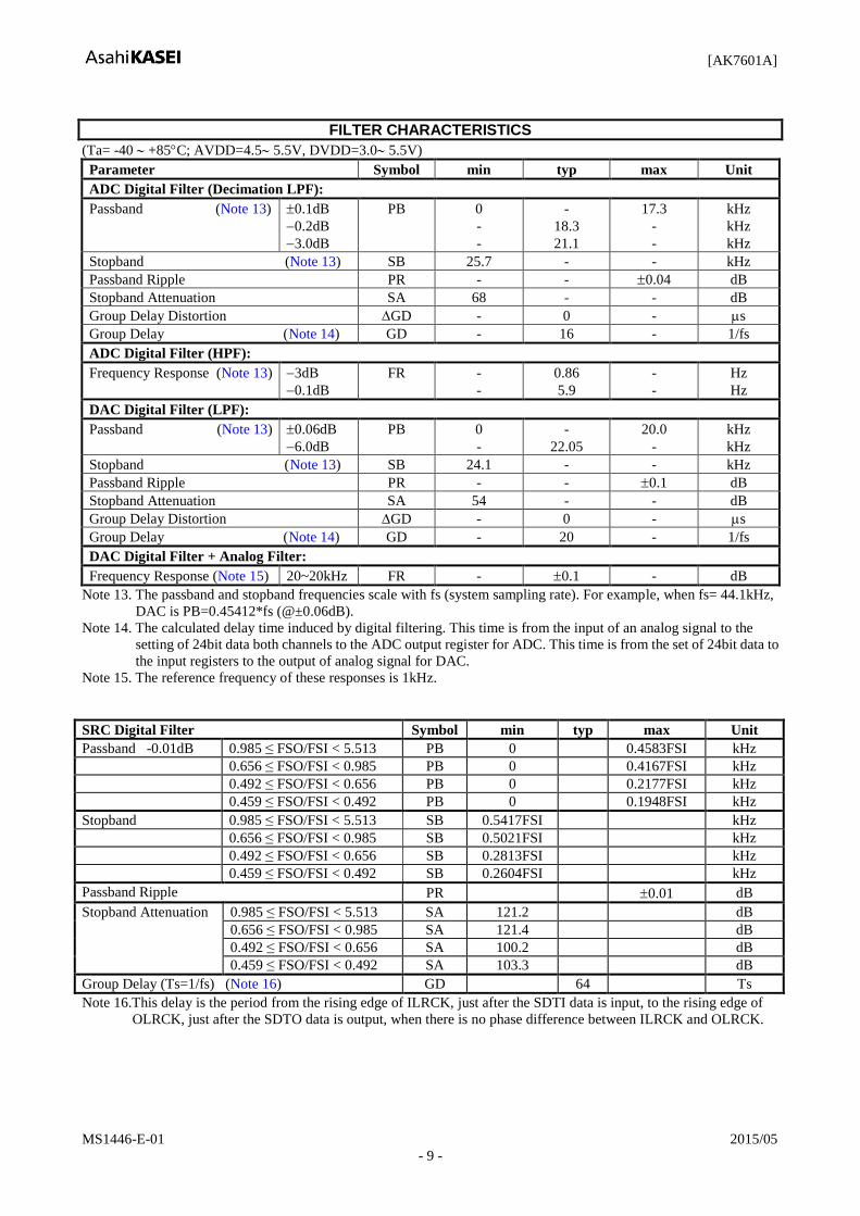
FILTER CHARACTERISTICS
(Ta= -40 +85C; AVDD=4.5 5.5V, DVDD=3.0 5.5V)
Parameter Symbol min typ max Unit
ADC Digital Filter (Decimation LPF):
Passband (Note 13)
0.1dB
0.2dB
3.0dB
PB
0
-
-
-
18.3
21.1
17.3
-
-
kHz
kHz
kHz
Stopband (Note 13) SB 25.7 - - kHz
Passband Ripple PR - - 0.04 dB
Stopband Attenuation SA 68 - - dB
Group Delay Distortion GD - 0 - s
Group Delay (Note 14) GD - 16 - 1/fs
ADC Digital Filter (HPF):
Frequency Response (Note 13)
3dB
0.1dB
FR
-
-
0.86
5.9
-
-
Hz
Hz
DAC Digital Filter (LPF):
Passband (Note 13)
0.06dB
6.0dB
PB
0
-
-
22.05
20.0
-
kHz
kHz
Stopband (Note 13) SB 24.1 - - kHz
Passband Ripple PR - - 0.1 dB
Stopband Attenuation SA 54 - - dB
Group Delay Distortion GD - 0 - s
Group Delay (Note 14) GD - 20 - 1/fs
DAC Digital Filter + Analog Filter:
Frequency Response (Note 15) 20~20kHz FR - 0.1 - dB
Note 13. The passband and stopband frequencies scale with fs (system sampling rate). For example, when fs= 44.1kHz,
DAC is PB=0.45412*fs (@±0.06dB).
Note 14. The calculated delay time induced by digital filtering. This time is from the input of an analog signal to the
setting of 24bit data both channels to the ADC output register for ADC. This time is from the set of 24bit data to
the input registers to the output of analog signal for DAC.
Note 15. The reference frequency of these responses is 1kHz.
SRC Digital Filter Symbol min typ max Unit
Passband -0.01dB 0.985 ≤ FSO/FSI < 5.513 PB 0 0.4583FSI kHz
0.656 ≤ FSO/FSI < 0.985 PB 0 0.4167FSI kHz
0.492 ≤ FSO/FSI < 0.656 PB 0 0.2177FSI kHz
0.459 ≤ FSO/FSI < 0.492 PB 0 0.1948FSI kHz
Stopband 0.985 ≤ FSO/FSI < 5.513 SB 0.5417FSI kHz
0.656 ≤ FSO/FSI < 0.985 SB 0.5021FSI kHz
0.492 ≤ FSO/FSI < 0.656 SB 0.2813FSI kHz
0.459 ≤ FSO/FSI < 0.492 SB 0.2604FSI kHz
Passband Ripple PR 0.01 dB
Stopband Attenuation 0.985 ≤ FSO/FSI < 5.513 SA 121.2 dB
0.656 ≤ FSO/FSI < 0.985 SA 121.4 dB
0.492 ≤ FSO/FSI < 0.656 SA 100.2 dB
0.459 ≤ FSO/FSI < 0.492 SA 103.3 dB
Group Delay (Ts=1/fs) (Note 16) GD 64 Ts
Note 16.This delay is the period from the rising edge of ILRCK, just after the SDTI data is input, to the rising edge of
OLRCK, just after the SDTO data is output, when there is no phase difference between ILRCK and OLRCK.

[AK7601A]
MS1446-E-01 2015/05
- 10 -
DC CHARACTERISTICS
(Ta=-40C+85C; AVDD= 4.55.5V, DVDD=3.05.5V)
Parameter Symbol min typ max Unit
High-Level Input Voltage
(PDN, SDA, SCL, SDTI1-4, ILRCK1-3, IBICK1-3,
MUTEN, XTI pins)
(CLKMODE pin)
Low-Level Input Voltage
(PDN, SDA, SCL, SDTI1-4, ILRCK1-3, IBICK1-3,
MUTEN, XTI pins)
(CLKMODE pin)
VIH
VIH
VIL
VIL
70%DVDD
80%DVDD
-
-
-
-
-
-
-
-
30%DVDD
20%DVDD
V
V
V
V
High-Level Output Voltage
(SDTO1-3, OLRCK, OBICK, OMCLK, SDA, DZF pins:
Iout=-100µA)
Low-Level Output Voltage
(SDTO1-3, OLRCK, OBICK, OMCLK, DZF pins:
Iout= 100µA)
(SDA pin: Iout= 3mA)
VOH
VOL
VOL
DVDD-0.5
-
-
-
-
-
-
0.5
0.4
V
V
V
Input Leakage Current PDN, SDA, SCL, SDTI1-4,
ILRCK1-3, IBICK1-3,
MUTEN, XTI
Iin - - 10 µA
[AK7601A]
MS1446-E-01 2015/05
- 11 -
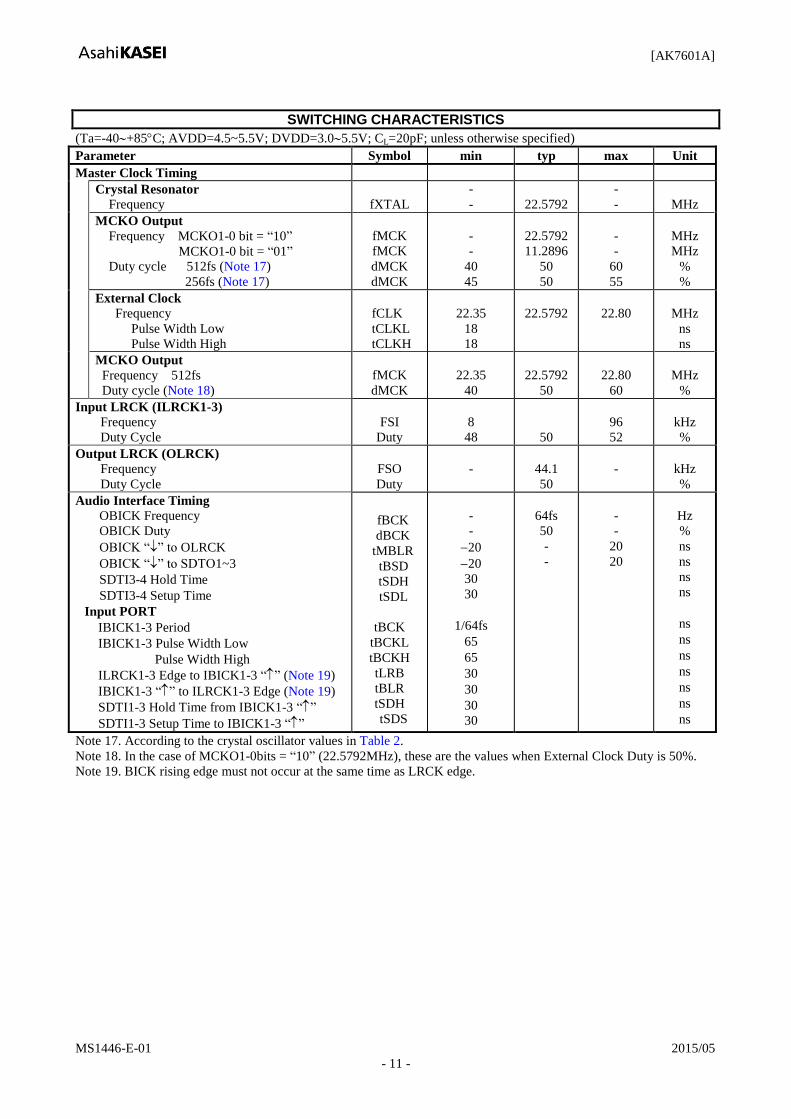
SWITCHING CHARACTERISTICS
(Ta=-40+85C; AVDD=4.5~5.5V; DVDD=3.05.5V; CL=20pF; unless otherwise specified)
Parameter Symbol min typ max Unit
Master Clock Timing
Crystal Resonator
Frequency
fXTAL
-
-
22.5792
-
-
MHz
MCKO Output
Frequency MCKO1-0 bit = “10”
MCKO1-0 bit = “01” Duty cycle 512fs (Note 17)
256fs (Note 17)
fMCK
fMCK
dMCK
dMCK
-
-
40
45
22.5792
11.2896
50
50
-
-
60
55
MHz
MHz
%
%
External Clock
Frequency
Pulse Width Low
Pulse Width High
fCLK
tCLKL
tCLKH
22.35
18
18
22.5792
22.80
MHz
ns
ns
MCKO Output
Frequency 512fs
Duty cycle (Note 18)
fMCK
dMCK
22.35
40
22.5792
50
22.80
60
MHz
%
Input LRCK (ILRCK1-3)
Frequency
Duty Cycle
FSI
Duty
8
48
50
96
52
kHz
%
Output LRCK (OLRCK)
Frequency
Duty Cycle
FSO
Duty
-
44.1
50
-
kHz
%
Audio Interface Timing
OBICK Frequency
OBICK Duty
OBICK “” to OLRCK
OBICK “” to SDTO1~3
SDTI3-4 Hold Time
SDTI3-4 Setup Time
Input PORT
IBICK1-3 Period
IBICK1-3 Pulse Width Low
Pulse Width High
ILRCK1-3 Edge to IBICK1-3 “” (Note 19)
IBICK1-3 “” to ILRCK1-3 Edge (Note 19)
SDTI1-3 Hold Time from IBICK1-3 “”
SDTI1-3 Setup Time to IBICK1-3 “”
fBCK
dBCK
tMBLR
tBSD
tSDH
tSDL
tBCK
tBCKL
tBCKH
tLRB
tBLR
tSDH
tSDS
-
-
20
20
30
30
1/64fs
65
65
30
30
30
30
64fs
50
-
-
-
-
20
20
Hz
%
ns
ns
ns
ns
ns
ns
ns
ns
ns
ns
ns
Note 17. According to the crystal oscillator values in Table 2.
Note 18. In the case of MCKO1-0bits = “10” (22.5792MHz), these are the values when External Clock Duty is 50%.
Note 19. BICK rising edge must not occur at the same time as LRCK edge.

[AK7601A]
MS1446-E-01 2015/05
- 12 -
Parameter Symbol min typ max Unit
Control Interface Timing (I2C Bus mode):
SCL Clock Frequency
Bus Free Time Between Transmissions
Start Condition Hold Time (prior to first clock pulse)
Clock Low Time
Clock High Time
Setup Time for Repeated Start Condition
SDA Hold Time from SCL Falling (Note 20)
SDA Setup Time from SCL Rising
Rise Time of Both SDA and SCL Lines
Fall Time of Both SDA and SCL Lines
Setup Time for Stop Condition
Pulse Width of Spike Noise Suppressed by Input Filter
Capacitive load on bus
fSCL
tBUF
tHD:STA
tLOW
tHIGH
tSU:STA
tHD:DAT
tSU:DAT
tR
tF
tSU:STO
tSP
Cb
-
1.3
0.6
1.3
0.6
0.6
0
0.1
-
-
0.6
0
-
400
-
-
-
-
-
-
-
0.3
0.3
-
50
400
kHz
s
s
s
s
s
s
s
s
s
s
ns
pF
Power-up Timing
DVDD to AVDD
tPU
>0
ns
Power-down & Reset Timing
PDN “L” Width after AVDD is ON (Note 21)
PDN Pulse Width (Note 21)
tPD1
tPD2
150
200
ns
ms
Note 20. Data must be held long enough to bridge the 300ns-transition time of SCL.
Note 21. The AK7601A can be reset by bringing the PDN pin = “L”. The PDN pin must held “L” for more than 200 ms for
a certain reset.
Note 22. I2C-bus is a trademark of NXP B.V.

[AK7601A]
MS1446-E-01 2015/05
- 13 -
Timing Diagram
Figure 3. Clock Timing
tLRB
LRCK1-3
VIH BICK1-3
VIL
VIH
VIL
tBLR
tSDS
SDTI1-3 VIH
VIL
tSDH
Figure 4. Audio Interface Timing (Input Port)
1/fCLK
tCLKL
VIH
tCLKH
XTI VIL
1/fMCK
50%DVDD MCKO
tdMCKL tdMCKH dMCK = tdMCKH (or tdMCKL) x fMCK x 100
1/fBCK
tdBCKL tdBCKH
BICK 50%DVDD
1/fs
LRCK 50%DVDD
tdLRKL tdLRKH dLRK = tdLRKH (or tdLRKL) x fs x 100
dBCK = tdBCKH (or tdBCKL) x fs x 100

[AK7601A]
MS1446-E-01 2015/05
- 14 -
OLRCK
OBICK
SDTO1-3
tBSD
tMBLR
50%DVDD
50%DVDD
50%DVDD
SDTI4
tSDH tSDS
VIH
VIL
Figure 5. Audio Interface Timing (Output Port)
Figure 6. I2C Bus Mode Timing
PDN
AVDD
DVDD
“L” “H”
VIL
VIH
tPD2 tPD1
“L” “H”
tPU
Figure 7. Power Up & Power Down Timing
tHIGH
SCL
SDA
VIH
tLOW tBUF
tHD:STA
tR tF
tHD:DAT tSU:DAT tSU:STA
Stop Start Start Stop
tSU:STO
VIL
VIH
VIL
tSP

[AK7601A]
MS1446-E-01 2015/05
- 15 -
OPERATION OVERVIEW
System Clock
The external clock input or X’tal input is available for MCLK clock source. (Figure 8, Figure 9) The required clock is
22.579MHz MCLK only.
In the normal operation, if the clock is stopped, click noise may occur when the clock supply is restarted. It can be
prevented by external mute.
OLRCK MCKO (MHz) OBICK (MHz)
44.1kHz 22.5792 2.8224
Table 1. System Clock Example
Clock Source
The clock for the XTI pin can be generated by two methods:
1) External Clock (CLKMODE pin= “H”)
XTI
XTO AK7601A
External Clock
Figure 8. External Clock Mode
Note. Do not input the clock over DVDD.
2) X’tal (CLKMODE pin= “L”)
XTI
XTO
AK7601A
Figure 9. X’tal Mode
C0 L1 C1 R1 CL
0.78pF~1.2pF 20.475mH~11.8mH 2.428fF~4.2fH 24.1Ω~16.0Ω 12pF~8pF
Table 2. Recommended Parameters of Crystal Oscillator
R1 C1 L1
C0
CL CL
Figure 10. Equivalent Circuit and Load Capacitance of Crystal Oscillator

[AK7601A]
MS1446-E-01 2015/05
- 16 -
Digital High Pass Filter
The ADC has a digital high pass filter for DC offset cancellation. The cut-off frequency of the HPF is 0.86Hz.
Master Clock Output Pin
The MCKO pin is the output pin for master clock. MCKO1-0 bits control the master clock frequency.
MCKO1 bit MCKO0 bit Master Clock Speed
0 0 “L” Output (default)
0 1 256fs (11.2896MHz)
1 0 512fs (22.5792MHz)
1 1 Reserved
Table 3. Master Clock Output Select
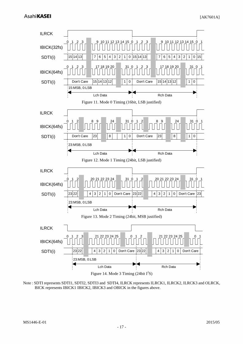
Audio Interface Input Format
In all modes the serial data is MSB-first, two’s complement format and SDTI1-4 are latched on the rising edge of
IBICK1-3 and OBICK respectively.
IDIF1-0 bits setting is reflected on SDTI1-3 and IDIF41-40 bits setting is reflected on SDIT4.
Use OLRCK, OBICK and IDIF when the SDTI3 data is input to Input2 instead of being used for SRC.
Mode IDIF1 bit IDIF0 bit SDTI1-3 Format ILRCK1-3
pins
IBICK1-3
pins
IBICK1-3
Freq
0 0 0 16bit, LSB justified
Input Input
32~64fs
1 0 1 24bit, LSB justified 48~64fs
2 1 0 24bit, MSB justified 48~64fs
3 1 1 24 or 16bit I
2S Compatible 48~64fs (default)
16bit, I2S Compatible 32fs
Table 4. SDTI1~3 Input Audio Interface Format
Mode IDIF41 bit IDIF40 bit SDTI4 Format OLRCK
pin
OBICK
pin
OBICK
Freq
0 0 0 16bit, LSB justified
Output Output 64fs
1 0 1 24bit, LSB justified
2 1 0 24bit, MSB justified
3 1 1 24 or 16bit I2S Compatible (default)
Table 5. SDTI4 Input Audio Interface Format
[AK7601A]
MS1446-E-01 2015/05
- 17 -
ILRCK
IBICK(32fs)
0 1 102 3 9 11 12 13 14 15 0 1 2 3 10109 11 12 13 14 15
SDTI(i) Don't Care 1 0 15 14 13 2 1 015 14 13 12 12Don't Care
15:MSB, 0:LSB
SDTI(i) 15 14 13 7 6 5 4 3 2 1 0 15 14 13 157 6 5 4 3 2 1 0
IBICK(64fs)
0 1 182 3 19 20 31 0 1 2 3 1018 19 20 3117 17
Lch Data Rch Data
Figure 11. Mode 0 Timing (16bit, LSB justified)
ILRCK
IBICK(64fs)
0 1 2 24 31 0 1 2 1031248 9 8 9
SDTI(i) Don't Care 0 8 1 0
23:MSB, 0:LSB
Lch Data Rch Data
23 8 Don't Care 231
Figure 12. Mode 1 Timing (24bit, LSB justified)
ILRCK
IBICK(64fs)
0 1 2 20 21 24 31 0 1 2 102220 21 312422 23 23
SDTI(i) Don't Care0 0
23:MSB, 0:LSB
Lch Data Rch Data
Don't Care4 3 2 123 22 23 22 231234
Figure 13. Mode 2 Timing (24bit, MSB justified)
ILRCK
IBICK(64fs)
0 1 2 2521 24 0 1 2 1022 2521 2422 23 233
SDTI(i) Don't Care0 0
23:MSB, 0:LSB
Lch Data Rch Data
Don't Care4 3 2 123 22 23 22 1234
Figure 14. Mode 3 Timing (24bit I
2S)
Note : SDTI represents SDTI1, SDTI2, SDTI3 and SDTI4, ILRCK represents ILRCK1, ILRCK2, ILRCK3 and OLRCK,
BICK represents IBICK1 IBICK2, IBICK3 and OBICK in the figures above.
[AK7601A]
MS1446-E-01 2015/05
- 18 -
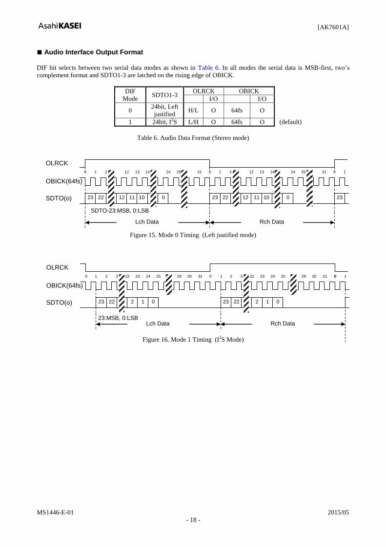
Audio Interface Output Format
DIF bit selects between two serial data modes as shown in Table 6. In all modes the serial data is MSB-first, two’s
complement format and SDTO1-3 are latched on the rising edge of OBICK.
DIF
Mode SDTO1-3
OLRCK OBICK
I/O I/O
0 24bit, Left
justified H/L O 64fs O
1 24bit, I2S L/H O 64fs O (default)
Table 6. Audio Data Format (Stereo mode)
Figure 15. Mode 0 Timing (Left justified mode)
Figure 16. Mode 1 Timing (I2S Mode)
OLRCK
OBICK(64fs)
SDTO(o)
0 1 2 12 13 14 24 25 31 0 1 2 12 13 14 24 25 31 0
23
1
22 0 23 22 12 11 10 0 23
Lch Data Rch Data
12 11 10
SDTO-23:MSB, 0:LSB
OLRCK
OBICK(64fs)
SDTO(o)
0 1 2 3 22 23 24 25 0 0 1 31 29 30
23 22 1
23:MSB, 0:LSB Lch Data Rch Data
2 0
2 3 22 23 24 25 0 31 29 30
23 22 1 2 0
1
[AK7601A]
MS1446-E-01 2015/05
- 19 -
Zero Detect Function
The AK7601A has independent zeros detect function for each DAC. This function is always enabled. Channel grouping
can be selected by DZD1-3 bits of CONT1 and its covers 6-channel outputs. Counting on “AND” for zero detected flags
of selected channels, when the input data is continuously zeros for 8192 LRCK cycles, the DZF pin goes to “H” if DZLH
bit (CONT1) is “0”, the DZF pin goes to “L” if DZLH bit (CONT1) is “1”. The DZF pin immediately returns to “L”
(DZLH bit “0”) or “H” (DZLH bit “1”) if the input data is not zero after the zero detection.
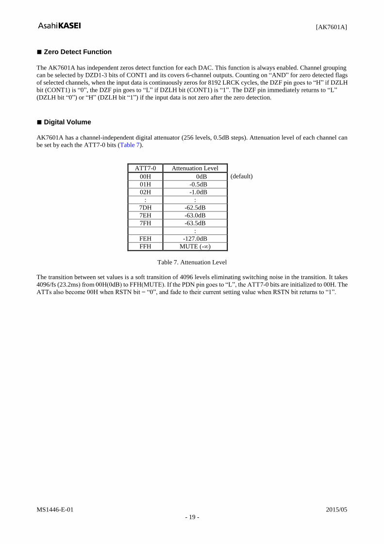
Digital Volume
AK7601A has a channel-independent digital attenuator (256 levels, 0.5dB steps). Attenuation level of each channel can
be set by each the ATT7-0 bits (Table 7).
ATT7-0 Attenuation Level
(default) 00H 0dB
01H -0.5dB
02H -1.0dB
: :
7DH -62.5dB
7EH -63.0dB
7FH -63.5dB
:
FEH -127.0dB
FFH MUTE (-∞)
Table 7. Attenuation Level
The transition between set values is a soft transition of 4096 levels eliminating switching noise in the transition. It takes
4096/fs (23.2ms) from 00H(0dB) to FFH(MUTE). If the PDN pin goes to “L”, the ATT7-0 bits are initialized to 00H. The
ATTs also become 00H when RSTN bit = “0”, and fade to their current setting value when RSTN bit returns to “1”.

[AK7601A]
MS1446-E-01 2015/05
- 20 -
Soft Mute (MUTE1, MUTE2) (Figure 33)
Soft mute operation is performed in the digital domain. When the MUTEN pin is set to “L” or SMUTE bit is set “0”, the
output signal is attenuated to -∞ in the time set by MCONT bit. When the SMUTE bit is returned to “1”, the mute is
cancelled and the output attenuation level gradually changes to 0dB in the time set by MCONT bit. If the soft mute is
cancelled before attenuating -∞, the attenuation is discontinued and the attenuation level is returned to 0dB by the same
cycle. Soft mute is effective for changing the signal source without stopping the signal transmission.
MUTEN pin or SMUTEN bit
ATT Level
DZF
D-Volume1 Full Level
-
AOUT
8192/fs
GD GD
(1)
(4)
(5)
(6)
(3)
(2)
(2)
Note:
(1) The transition time to attenuate input data to -∞ in linear steps is set by MCONT bit.
(2) There is delay, which is set by the Delay block, from a falling edge of the MUTEN pin or SMUTEN bit to start the
attenuation.
(3) The transition time to return to the full scale of the input signal to LG1, RG1, LG2 and RG2 is set by MCONT bit.
(4) Analog output corresponding to digital input has a group delay (GD).
(5) If the soft mute is cancelled before attenuating -∞ after starting the operation, the attenuation is discontinued and
the digital volume is returned to the full scale level by the same cycle.
(6) When the input data for both channels are continuously zero for 8192 LRCK cycles and DZLH bit is “0”, the DZF
pin goes to “H” (the DZF pin goes to “L” if the DZLH bit is “1”). The DZF pin immediately returns to “L” if the
input data are not zero after going to DZF “H” (DZLH bit =“0”).
Figure 17. Soft Mute and Zero Detect Function
[AK7601A]
MS1446-E-01 2015/05
- 21 -
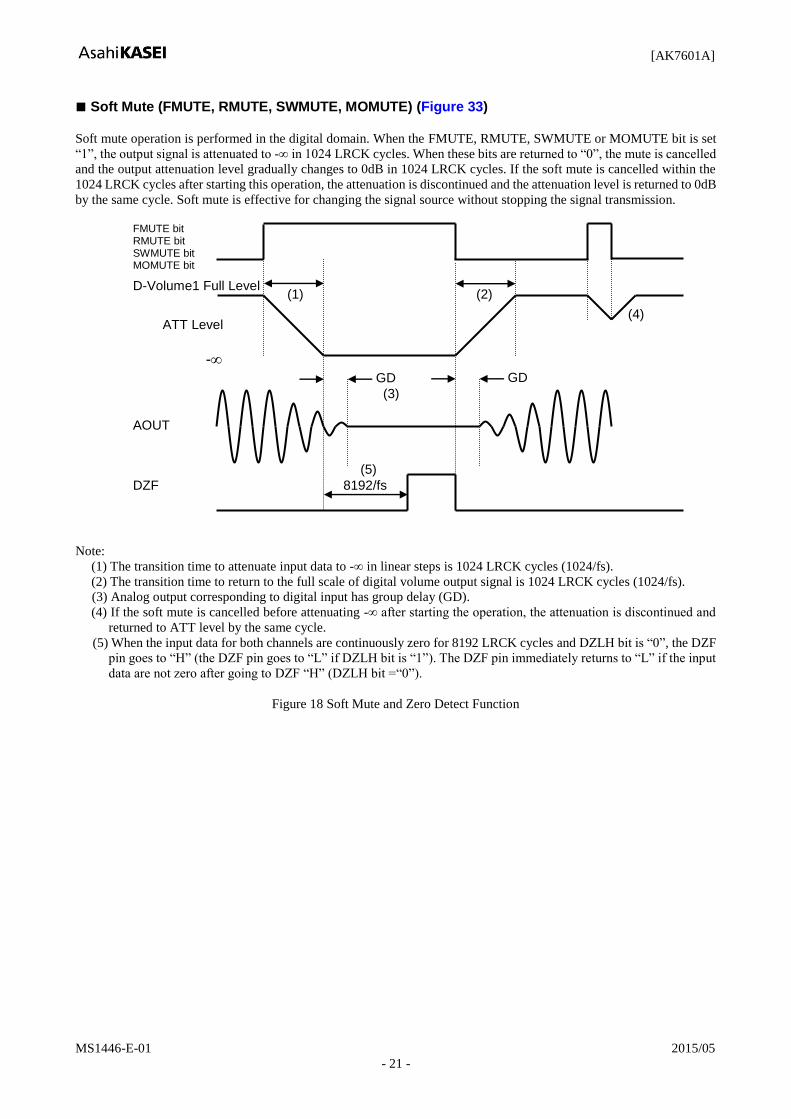
Soft Mute (FMUTE, RMUTE, SWMUTE, MOMUTE) (Figure 33)
Soft mute operation is performed in the digital domain. When the FMUTE, RMUTE, SWMUTE or MOMUTE bit is set
“1”, the output signal is attenuated to -∞ in 1024 LRCK cycles. When these bits are returned to “0”, the mute is cancelled
and the output attenuation level gradually changes to 0dB in 1024 LRCK cycles. If the soft mute is cancelled within the
1024 LRCK cycles after starting this operation, the attenuation is discontinued and the attenuation level is returned to 0dB
by the same cycle. Soft mute is effective for changing the signal source without stopping the signal transmission.
DZF
-
AOUT
8192/fs
GD GD
(1)
(3)
(4)
(5)
(2)
FMUTE bit RMUTE bit SWMUTE bit MOMUTE bit
ATT Level
D-Volume1 Full Level
Note:
(1) The transition time to attenuate input data to -∞ in linear steps is 1024 LRCK cycles (1024/fs).
(2) The transition time to return to the full scale of digital volume output signal is 1024 LRCK cycles (1024/fs).
(3) Analog output corresponding to digital input has group delay (GD).
(4) If the soft mute is cancelled before attenuating -∞ after starting the operation, the attenuation is discontinued and
returned to ATT level by the same cycle.
(5) When the input data for both channels are continuously zero for 8192 LRCK cycles and DZLH bit is “0”, the DZF
pin goes to “H” (the DZF pin goes to “L” if DZLH bit is “1”). The DZF pin immediately returns to “L” if the input
data are not zero after going to DZF “H” (DZLH bit =“0”).
Figure 18 Soft Mute and Zero Detect Function

[AK7601A]
MS1446-E-01 2015/05
- 22 -
Pseudo-Differential Input (AINL1/AINR1, AINL2/AINR2)
The AK7601A has two sets of pseudo-differential input channels.
+
-
+
-
-
+
AAF
AAF
VCOM=AVDD/2
LIN1
RIN1
GND1
Figure 19. Pseudo-Differential Input Block
When power-on the AK7601A, capacitors that connected to the pseudo-differential input pin are charged in high speed
(Fast mode). This first mode is controlled by a register (FCHA0 bit). The charging time in fast mode is 40ms (typ) and
100ms (max).
(01H: D4 bit)
FCHA0 Fast Charge
1 ON (default)
0 OFF
Table 8. Fast Charge
Input Selector
The AK7601A has an analog input selector for ADC and a digital input selector for SRC. SEL01-00 bits and SEL11-10
bits control these input selectors. Click noise may occur when SEL01-00 bits and SEL11-10 bits are changed. Mute digital
output if the click noise affects system performance.
SEL01 SEL00 ADC Input
0 0 AINL1/AINR1 (default)
0 1 AINL2/AINR2
1 0 AINL3/AINR3
1 1 AINL4/AINR4
Table 9. Analog Input Selector
SEL11 SEL10 SRC Input
0 0 SDTI1 (default)
0 1 SDTI2
1 0 SDTI 3
1 1 Reserved
Table 10. Digital Input Selector

[AK7601A]
MS1446-E-01 2015/05
- 23 -
Power-up Sequence
The PDN pin must be “L” until all power supplies are ON. AVDD must be supplied after DVDD is ON.
PDN
AVDD
DVDD
“L” “H”
Figure 20. Power-up Sequence
System Reset
The internal regulator will be powered-up by inputting the master clock to the XTI pin or connecting a X’tal after setting
the PDN pin to “H”. In X’tal mode, the internal regulator is powered-up in 5ms after the PDN pin becomes “H”. In
external clock mode, the internal regulator is powered-up in 5ms after clock input. When the regulator is powered-up, the
internal master clock starts by setting RSTN bit to “1”.

[AK7601A]
MS1446-E-01 2015/05
- 24 -
Power Down
The ADC and DAC parts of the AK7601A are placed in the power-down mode by bringing the PDN pin “L” and the
digital filter is also reset at the same time. The internal registers are initiated to their default value by the PDN pin = “L”.
This reset should always be made after power-up. In the power-down mode, SDTO1/SDTO3, SDTO2/SDTI4, OBICK,
OLRCK and DZF pins go to “L” and the analog output is VSS. When exiting the power-down mode, the AK7601A will
be in reset state since the RSTN bit = “0”. Figure 21 shows the power on/off sequence example.
PDN
ADC Internal
State Normal Operation Power Down
RSTN
DAC Internal
State Normal Operation Power Down
SDTO1~3
ADC In
(Analog)
GD(4)
DAC Out
(Analog)
GD(4)
Clock In
XTI(external)
DZF
DZLH= “1”
DZLH= “0”
“0” data(5)
(7)
(9)
(6)
(8)
PDN Internal 5ms(1)
Clock In
X'tal
(10)
(2)
Regulator Normal Operation Power Down (3)
Note:
(1) After the PDN pin = “H”, the internal PDN is “L” until X’tal and regulator are powered-up. (Register writing is not
valid for 5ms of this period)
(2) During the RSTN bit is “0”, all circuits will be powered down except the regulator and X’tal even when the
internal PDN is “H”.
(3) Regulator will be powered-up after the PDN pin becomes “H”.
(4) The DAC and SDTO1-3 outputs corresponding to the ADC input has group delay (GD).
(5) The SDTP1-3 outputs are “0” when the AK7601A is powered-down.
(6) The DAC output is VSS voltage when the AK7601A is powered-down.
(7) Click noise occurs at the falling edge of PDN.
(8) In case of connecting a X’tal, the clock output is “L” when the PDN pin =“L”. The X’tal will be powered up after
the PDN pin =“H”.
(9) In power down mode (PDN pin = “L”), the DZF pin = “L”.
(10) The DZF pin output will reflects the DZLH bit setting when internal PDN is “H”.
Figure 21. Power Up/Down Sequence Example
[AK7601A]
MS1446-E-01 2015/05
- 25 -
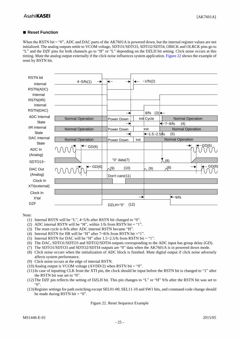
Reset Function
When the RSTN bit = “0”, ADC and DAC parts of the AK7601A is powered down, but the internal register values are not
initialized. The analog outputs settle to VCOM voltage, SDTO1/SDTO3, SDTO2/SDTI4, OBICK and OLRCK pins go to
“L” and the DZF pins for both channels go to “H” or “L” depending on the DZLH bit setting. Click noise occurs at this
timing. Mute the analog output externally if the click noise influences system application. Figure 22 shows the example of
reset by RSTN bit.
RSTN bit
ADC Internal
State Normal Operation Power Down
DAC Internal
State Normal Operation Power Down
SDTO13~
ADC In
(Analog)
GD(6)
DAC Out
(Analog)
GD(6)
Clock In
XTI(external)
Don't care(11)
DZF DZLH="0"
"0" data(7)
(9)
(12)
(9)
Internal
RSTN(ADC)
Clock In
X'tal
Internal
RSTN(IIR)
Internal
RSTN(DAC)
Init Cycle
8/fs
Normal Operation
Init
1.5~2.5/fs
Normal Operation IIR Internal
State Power Down Init
7~8/fs
Normal Operation
Normal Operation
4~5/fs(1)
(3)
(4)
(5)
GD(6)
(10) GD(6)
9/fs
~1/fs(2)
(8)
(8)
Note:
(1) Internal RSTN will be “L”, 4~5/fs after RSTN bit changed to “0”.
(2) ADC internal RSTN will be “H”, within 1/fs from RSTN bit = “1”.
(3) The reset cycle is 8/fs after ADC internal RSTN became “H”.
(4) Internal RSTN for IIR will be “H” after 7~8/fs from RSTN bit =“1”.
(5) Internal RSTN for DAC will be “H” after 1.5~2.5/fs from RSTN bit = “1”.
(6) The DAC, SDTO1/SDTO3 and SDTO2/SDTI4 outputs corresponding to the ADC input has group delay (GD).
(7) The SDTO1/SDTO3 and SDTO2/SDTI4 outputs are “0” data when the AK7601A is in powered down mode.
(8) Click noise occurs when the initialization of ADC block is finished. Mute digital output if click noise adversely
affects system performance.
(9) Click noise occurs at the edge of internal RSTN.
(10) Analog output is VCOM voltage (AVDD/2) when RSTN bit = “0”.
(11) In case of inputting CLK from the XTI pin, the clock should be input before the RSTN bit is changed to “1” after
the RSTN bit was set to “0”.
(12) The DZF pin reflects the setting of DZLH bit. This pin changes to “L” or “H” 9/fs after the RSTN bit was set to
“0”.
(13) Register settings for path switching except SEL01-00, SEL11-10 and SW1 bits, and command code change should
be made during RSTN bit = “0”.
Figure 22. Reset Sequence Example

[AK7601A]
MS1446-E-01 2015/05
- 26 -
I2C BUS INTERFACE (Microcontroller Interface)
Access to the AK7601A registers and RAM is processed by I²C bus. The format of the I²C is complement with fast mode
(max: 400kHz). The AK7601A does not support Hs mode. (max: 3.4MHz).
Data Transfer
In order to access any IC devices on the I2C BUS, input a start condition first, followed by a single Slave address
which includes the Device Address. IC devices on the BUS compare this Slave address with their own addresses
and the IC device which has an identical address with the Slave-address generates an acknowledgement. An IC
device with the identical address then executes either a read or a write operation. After the command execution,
input a Stop condition.
1-1. Data Change
Change the data on the SDA line while SCL line is “L”. SDA line condition must be stable and fixed while the
clock is “H”. Change the Data line condition between “H” and “L” only when the clock signal on the SCL line is
“L”. Change the SDA line condition while SCL line is “H” only when the start condition or stop condition is input.
Figure 23. Data Transition
1-2. Start condition and Stop condition
Start condition is generated by the transition of “H” to “L” on the SDA line while the SCL line is “H”. All
instructions are initiated by Start condition. Stop condition is generated by the transition of “L” to “H” on SDA
line while SCL line is “H”. All instructions end by Stop condition.
Figure 24. Start Condition and Stop Condition
SCL
SDA
DATA LINE STABLE :
DATA VALID
CHANGE OF DATA ALLOWED
SCL
SDA
STOP CONDITION START CONDITION
[AK7601A]
MS1446-E-01 2015/05
- 27 -
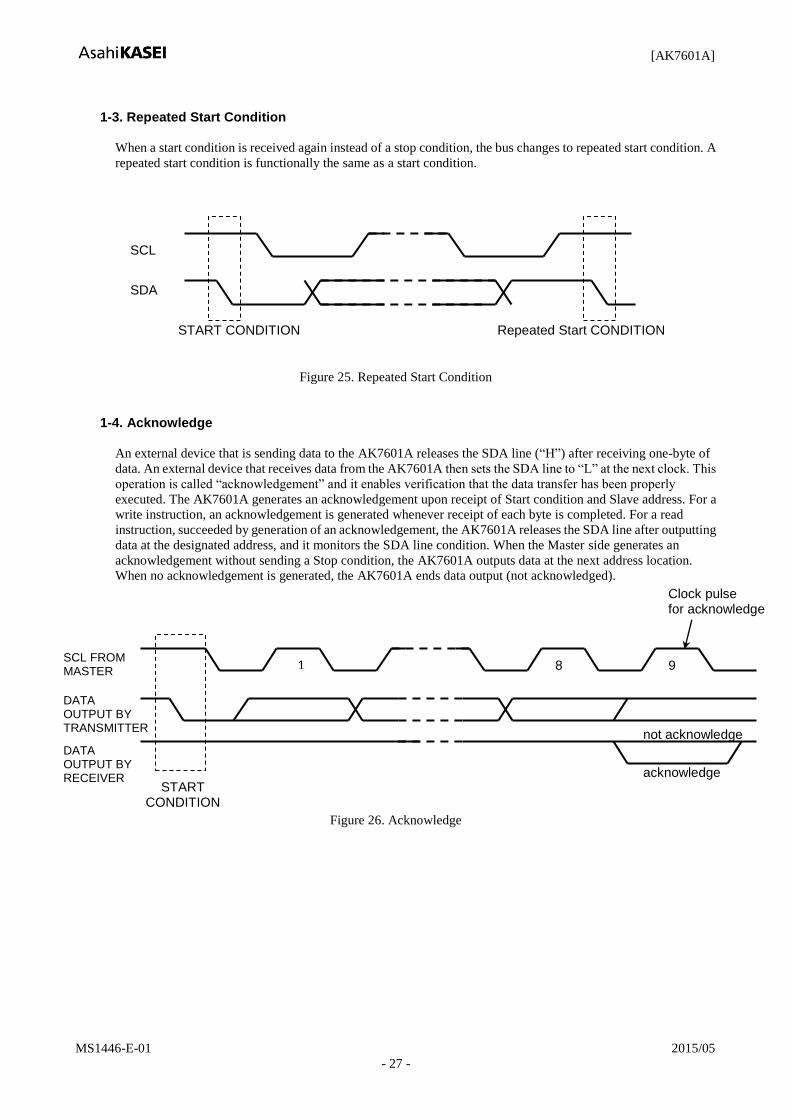
1-3. Repeated Start Condition
When a start condition is received again instead of a stop condition, the bus changes to repeated start condition. A
repeated start condition is functionally the same as a start condition.
Figure 25. Repeated Start Condition
1-4. Acknowledge
An external device that is sending data to the AK7601A releases the SDA line (“H”) after receiving one-byte of
data. An external device that receives data from the AK7601A then sets the SDA line to “L” at the next clock. This
operation is called “acknowledgement” and it enables verification that the data transfer has been properly
executed. The AK7601A generates an acknowledgement upon receipt of Start condition and Slave address. For a
write instruction, an acknowledgement is generated whenever receipt of each byte is completed. For a read
instruction, succeeded by generation of an acknowledgement, the AK7601A releases the SDA line after outputting
data at the designated address, and it monitors the SDA line condition. When the Master side generates an
acknowledgement without sending a Stop condition, the AK7601A outputs data at the next address location.
When no acknowledgement is generated, the AK7601A ends data output (not acknowledged).
Figure 26. Acknowledge
SCL
SDA
Repeated Start CONDITION START CONDITION
SCL FROM MASTER
acknowledge
DATA OUTPUT BY TRANSMITTER
DATA OUTPUT BY RECEIVER
1 9 8
START CONDITION
Clock pulse for acknowledge
not acknowledge

[AK7601A]
MS1446-E-01 2015/05
- 28 -
1-5. The First byte
The First Byte which includes the Slave-address is input after the Start condition is set, and a target IC device that
will be accessed on the bus is selected by the Slave-address. The Slave-address is configured with the upper 7-bits.
Data of the upper 7-bits is “0011000”. The address bits that select the desired IC are fixed. When the Slave-address
is inputted, an external device that has the identical device address generates an acknowledgement and
instructions are then executed. The 8th bit of the First Byte (lowest bit) is allocated as the R/W Bit. When the R/W
Bit is “1”, the read instruction is executed, and when it is “0”, the write instruction is executed.
Note 23. In this document, there is a case that describes a “Write Slave-address assignment” when both address
bits match and a Slave-address at R/W Bit = “0” is received. There is a case that describes “Read
Slave-address assignment” when both address bits matches and a Slave-address at R/W Bit = “1” is
received.
0 0 1 1 0 0 0 R/W
Slave Address is fixed 30H(write) or 31H(read).
Figure 27. The First Byte Structure
1-6. The Second and Succeeding Bytes
The data format of the second and succeeding bytes of the AK7601A Transfer / Receive Serial data (command
code, address and data in microcontroller interface format) on the I2C BUS are all configured with a multiple of
8-bits. When transferring or receiving those data on the I2C BUS, they are divided into an 8-bit data stream
segment and they are transferred / received with the MSB side data first with an acknowledgement in-between.
When transferring / receiving A1B2C3 (hex) 24-bit serial data in microprocessor interface format:
Figure 28. Division of the Data
Note 24. In this document, there is a case that describes a write instruction command code which is received at the second
byte as “Write Command”. There is a case that describes a read instruction command code which is received at
the second byte as “Read Command”
A1 B2 C3
A A
8BIT 8BIT 8BIT
A Acknowledge
(1)I2C Format

[AK7601A]
MS1446-E-01 2015/05
- 29 -
Command Code
BIT7 BIT6 BIT5 BIT4 BIT3 BIT2 BIT1 BIT0
8/16(*1)/16(*2)/32 flag Area to be accessed
(1) 8/16(*1)/16(*2)/32 flag
When BIT[7:6] bits are “00”, the following data will be 8bit. The data will be 16bit 1word in 2byte transfer when “01”,
16bit 1word x 5 in 10byte transfer when “10”, and 32bit 1word x 5 in 20byte transfer when “11”.
(2) Accompanying data to the access area
BIT7 BIT6 BIT5 BIT4 BIT3 BIT2 BIT1 BIT0 Command and Content
0 0 0 0 0 0 0 1 01H Control Register CONT1 Setting
0 0 0 0 0 0 1 0 02H Control Register CONT2 Setting
0 0 0 0 0 0 1 1 03H Control Register CONT3 Setting
0 0 0 0 0 1 0 0 04H Control Register CONT4 Setting
0 0 0 0 0 1 0 1 05H Control Register CONT5 Setting
0 0 0 0 0 1 1 0 06H Control Register LOUT1VOL Setting
0 0 0 0 0 1 1 1 07H Control Register ROUT1VOL Setting
0 0 0 0 1 0 0 0 08H Control Register LOUT2VOL Setting
0 0 0 0 1 0 0 1 09H Control Register ROUT2VOL Setting
0 0 0 0 1 0 1 0 0AH Control Register LOUT3VOL Setting
0 0 0 0 1 0 1 1 0BH Control Register ROUT3VOL Setting
0 0 0 0 1 1 0 0 0CH Control Register MONOLVOL Setting
0 0 0 0 1 1 0 1 0DH Control Register MONORVOL Setting
0 0 0 0 1 1 1 0 0EH Control Register SWCONT1 Setting
0 0 0 0 1 1 1 1 0FH Control Register SWCONT2 Setting
0 1 0 0 0 0 0 0 40H EQ Gain1 Setting
0 1 0 0 0 0 0 1 41H EQ Gain2 Setting
0 1 0 0 0 0 1 0 42H Cross Over Fout Gain Setting
0 1 0 0 0 0 1 1 43H Cross Over Rout Gain Setting
0 1 0 0 0 1 0 0 44H Cross Over SWout Gain Setting
0 1 0 0 0 1 0 1 45H FrontL1 Delay Setting
0 1 0 0 0 1 1 0 46H FrontR1 Delay Setting
0 1 0 0 0 1 1 1 47H RearL2 Delay Setting
0 1 0 0 1 0 0 0 48H RearR2 Delay Setting
0 1 0 0 1 0 0 1 49H SWL3 Delay Setting
0 1 0 0 1 0 1 0 4AH SWR3 Delay Setting
0 1 0 1 0 0 0 0 50H Read SpeAna 1Band (125Hz)
0 1 0 1 0 0 0 1 51H Read SpeAna 2Band (500Hz)
0 1 0 1 0 0 1 0 52H Read SpeAna 3Band (2KHz)
0 1 0 1 0 0 1 1 53H Read SpeAna 4Band (8KHz)

[AK7601A]
MS1446-E-01 2015/05
- 30 -
BIT7 BIT6 BIT5 BIT4 BIT3 BIT2 BIT1 BIT0 Command and Content
1 0 0 0 0 0 0 0 80H Input Gain Setting
1 0 0 0 0 0 0 1 81H function1 Gain1 Setting
1 0 0 0 0 0 1 0 82H function1 Gain2 Setting
1 0 0 0 0 1 0 0 84H function1 in Filter Coefficient Setting Preparation
1 0 0 0 0 1 0 1 85H function1 out Filter Coefficient Setting Preparation
1 0 0 0 1 0 0 0 88H function2 LPF2 Filter Coefficient Setting Preparation
1 0 0 0 1 1 0 0 8CH function2 Gain1 Setting
1 0 0 0 1 1 0 1 8DH funciotn2 Gain Low Setting
1 0 0 1 0 0 0 0 90H Function3 Gain1 Coefficient Setting Preparation
1 0 0 1 0 0 0 1 91H Function3 Gain2 Coefficient Setting Preparation
1 0 0 1 0 0 1 0 92H Function3 Filter Coefficient Setting Preparation
1 0 0 1 0 0 1 1 93H Function4 Gain Coefficient Setting Preparation
1 0 0 1 0 1 0 0 94H Function5 Gain Coefficient Setting Preparation
1 0 0 1 0 1 0 1 95H Function5 Filter Coefficient Setting Preparation
1 0 0 1 0 1 1 0 96H EQ Bind2 Coefficient Setting Preparation
1 0 0 1 0 1 1 1 97H EQ Band5 Coefficient Setting Preparation
1 0 0 1 1 0 0 0 98H EQ Band6 Coefficient Setting Preparation
1 0 0 1 1 0 0 1 99H EQ Band7 Coefficient Setting Preparation
1 0 0 1 1 0 1 0 9AH EQ Band9 Coefficient Setting Preparation
1 0 0 1 1 0 1 1 9BH EQ Band12 Coefficient Setting Preparation
1 0 0 1 1 1 0 0 9CH EQ Band13 Coefficient Setting Preparation
1 0 0 1 1 1 0 1 9DH EQ Band14 Coefficient Setting Preparation
1 0 0 1 1 1 1 0 9EH X’ Over Filter1-3 Coefficient Setting Preparation
1 0 0 1 1 1 1 1 9FH SpeAna3Band Coefficient Setting Preparation
1 0 1 0 0 0 0 0 A0H SpeAna4Band Coefficient Setting Preparation
1 0 1 0 0 0 0 1 A1H FR Gain Setting
1 0 1 0 0 0 1 0 A2H SW Gain Setting
[AK7601A]
MS1446-E-01 2015/05
- 31 -
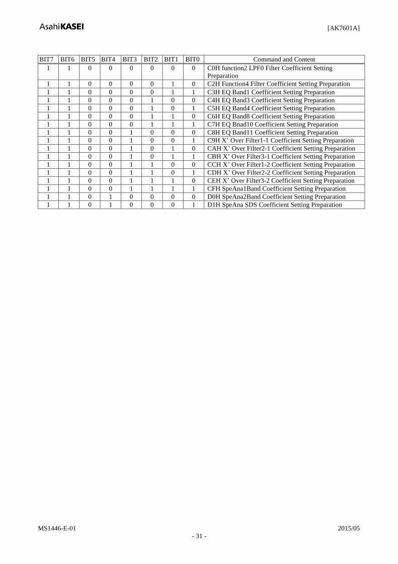
BIT7 BIT6 BIT5 BIT4 BIT3 BIT2 BIT1 BIT0 Command and Content
1 1 0 0 0 0 0 0 C0H function2 LPF0 Filter Coefficient Setting
Preparation
1 1 0 0 0 0 1 0 C2H Function4 Filter Coefficient Setting Preparation
1 1 0 0 0 0 1 1 C3H EQ Band1 Coefficient Setting Preparation
1 1 0 0 0 1 0 0 C4H EQ Band3 Coefficient Setting Preparation
1 1 0 0 0 1 0 1 C5H EQ Band4 Coefficient Setting Preparation
1 1 0 0 0 1 1 0 C6H EQ Band8 Coefficient Setting Preparation
1 1 0 0 0 1 1 1 C7H EQ Bnad10 Coefficient Setting Preparation
1 1 0 0 1 0 0 0 C8H EQ Band11 Coefficient Setting Preparation
1 1 0 0 1 0 0 1 C9H X’ Over Filter1-1 Coefficient Setting Preparation
1 1 0 0 1 0 1 0 CAH X’ Over Filter2-1 Coefficient Setting Preparation
1 1 0 0 1 0 1 1 CBH X’ Over Filter3-1 Coefficient Setting Preparation
1 1 0 0 1 1 0 0 CCH X’ Over Filter1-2 Coefficient Setting Preparation
1 1 0 0 1 1 0 1 CDH X’ Over Filter2-2 Coefficient Setting Preparation
1 1 0 0 1 1 1 0 CEH X’ Over Filter3-2 Coefficient Setting Preparation
1 1 0 0 1 1 1 1 CFH SpeAna1Band Coefficient Setting Preparation
1 1 0 1 0 0 0 0 D0H SpeAna2Band Coefficient Setting Preparation
1 1 0 1 0 0 0 1 D1H SpeAna SDS Coefficient Setting Preparation
[AK7601A]
MS1446-E-01 2015/05
- 32 -
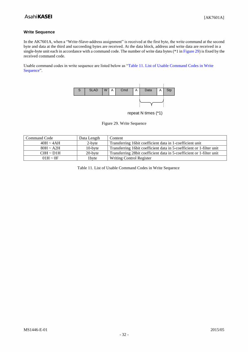
Write Sequence
In the AK7601A, when a “Write-Slave-address assignment” is received at the first byte, the write command at the second
byte and data at the third and succeeding bytes are received. At the data block, address and write data are received in a
single-byte unit each in accordance with a command code. The number of write data bytes (*1 in Figure 29) is fixed by the
received command code.
Usable command codes in write sequence are listed below as “Table 11. List of Usable Command Codes in Write
Sequence”.
Figure 29. Write Sequence
Command Code Data Length Content
40H ~ 4AH 2-byte Transferring 16bit coefficient data in 1-coefficient unit
80H ~ A2H 10-byte Transferring 16bit coefficient data in 5-coefficient or 1-filter unit
C0H ~ D1H 20-byte Transferring 28bit coefficient data in 5-coefficient or 1-filter unit
01H ~ 0F 1byte Writing Control Register
Table 11. List of Usable Command Codes in Write Sequence
S SLAD W Cmd Data A Stp A A
repeat N times (*1)

[AK7601A]
MS1446-E-01 2015/05
- 33 -
Data Format
Data Write
(1) Control Register Write
SDA
(1) COMMAND 01H~0F
(2) DATA D7~D0
(2) 16bit Coefficient (1-coefficient unit) or Delay Data Write
SDA
(1) COMMAND 40H~4AH
(2) DATA1-1 D15~D8
(3) DATA1-2 D7~D0
(3)16bit Coefficient (5-coefficient unit) Write
SDA
(1) COMMAND 80H~A2H
(2) DATA1-1 D15~D8
(3) DATA1-2 D7~D0
(4) DATA2-1 D15~D8
(5) DATA2-2 D7~D0
(6)~(11) (Continues in 2byte unit from DATA3 to DATA5. In total 10byte DATA)
(4)28bit Coefficient Data Write
SDA
(1) COMMAND C0H~D1H
(2) DATA1-1 0 0 0 0 D27~D24
(3) DATA1-2 D23~D16
(4) DATA1-3 D15~D8
(5) DATA1-4 D7~D0
(6)~(21) (Continues in 4byte unit from DATA2 to DATA5. In total 20byte DATA)

[AK7601A]
MS1446-E-01 2015/05
- 34 -
Read Sequence
In the AK7601A, when a “write- slave-address assignment” is received at the first byte, the command is send from micro
controller in the second byte. When the slave address is received after the start condition, the AK7601A starts outputting
the data regarding to command code.
When cancelling read operation before the AK7601A sends all data, assure that a “not acknowledged” signal is received
by the AK7601A. If this “not acknowledged” signal is not received, the AK7601A continues to send data until specified
number, and since it did not release the BUS, the stop condition cannot be properly received.
Usable command codes in read sequence are listed in Table 12
Figure 30. Read Sequence
Command Code Data Length Content
40H ~ 4AH 2-byte Reading 16bit coefficient data in 1-coefficient unit
80H ~ A2H 10-byte Reading 16bit coefficient data in 5-coefficient or 1-filter unit.
C0H ~ D1H 20-byte Reading 28bit coefficient data in 5-coefficient or 1-filter unit.
01H ~ 0F 1byte Reading Control Register
50H ~ 53H 2-byte Reading Spectrum Analyzer Data
Table 12. List of Usable Read Command Codes in Read Sequence
S SLAD W Cmd rS Data A A A SLAD R A
repeat N times
Data Na Stp
* Cancel
[AK7601A]
MS1446-E-01 2015/05
- 35 -
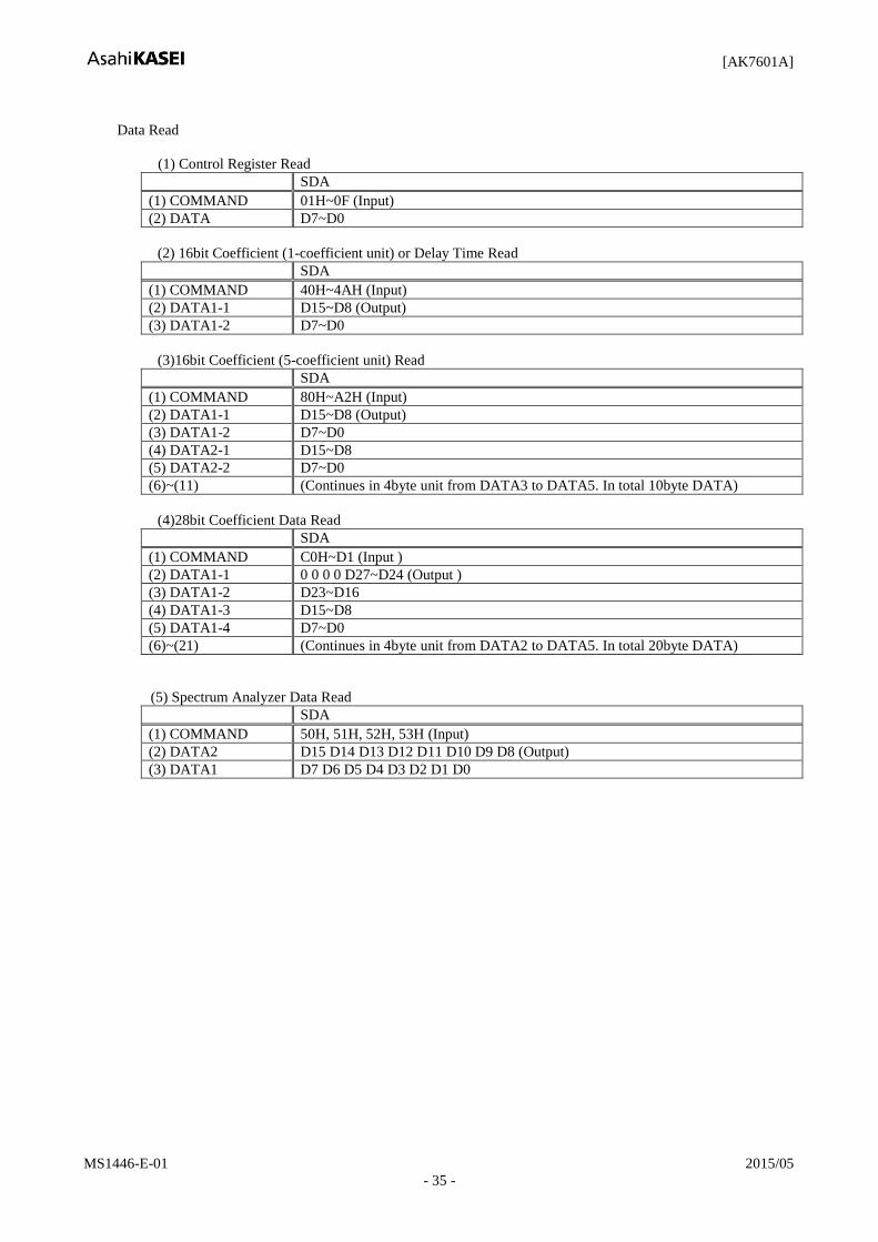
Data Read
(1) Control Register Read
SDA
(1) COMMAND 01H~0F (Input)
(2) DATA D7~D0
(2) 16bit Coefficient (1-coefficient unit) or Delay Time Read
SDA
(1) COMMAND 40H~4AH (Input)
(2) DATA1-1 D15~D8 (Output)
(3) DATA1-2 D7~D0
(3)16bit Coefficient (5-coefficient unit) Read
SDA
(1) COMMAND 80H~A2H (Input)
(2) DATA1-1 D15~D8 (Output)
(3) DATA1-2 D7~D0
(4) DATA2-1 D15~D8
(5) DATA2-2 D7~D0
(6)~(11) (Continues in 4byte unit from DATA3 to DATA5. In total 10byte DATA)
(4)28bit Coefficient Data Read
SDA
(1) COMMAND C0H~D1 (Input )
(2) DATA1-1 0 0 0 0 D27~D24 (Output )
(3) DATA1-2 D23~D16
(4) DATA1-3 D15~D8
(5) DATA1-4 D7~D0
(6)~(21) (Continues in 4byte unit from DATA2 to DATA5. In total 20byte DATA)
(5) Spectrum Analyzer Data Read
SDA
(1) COMMAND 50H, 51H, 52H, 53H (Input)
(2) DATA2 D15 D14 D13 D12 D11 D10 D9 D8 (Output)
(3) DATA1 D7 D6 D5 D4 D3 D2 D1 D0
[AK7601A]
MS1446-E-01 2015/05
- 36 -
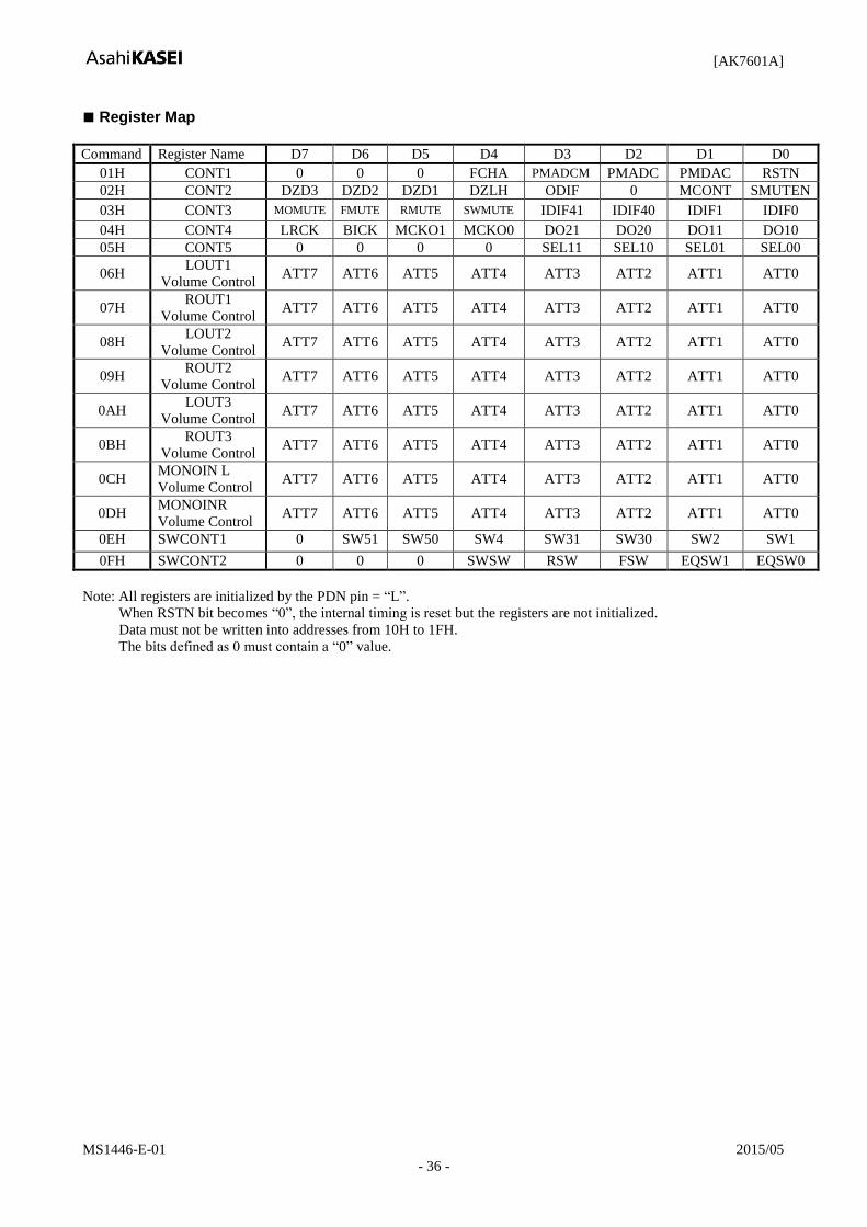
Register Map
Command Register Name D7 D6 D5 D4 D3 D2 D1 D0
01H CONT1 0 0 0 FCHA PMADCM PMADC PMDAC RSTN
02H CONT2 DZD3 DZD2 DZD1 DZLH ODIF 0 MCONT SMUTEN
03H CONT3 MOMUTE FMUTE RMUTE SWMUTE IDIF41 IDIF40 IDIF1 IDIF0
04H CONT4 LRCK BICK MCKO1 MCKO0 DO21 DO20 DO11 DO10
05H CONT5 0 0 0 0 SEL11 SEL10 SEL01 SEL00
06H LOUT1
Volume Control ATT7 ATT6 ATT5 ATT4 ATT3 ATT2 ATT1 ATT0
07H ROUT1
Volume Control ATT7 ATT6 ATT5 ATT4 ATT3 ATT2 ATT1 ATT0
08H LOUT2
Volume Control ATT7 ATT6 ATT5 ATT4 ATT3 ATT2 ATT1 ATT0
09H ROUT2
Volume Control ATT7 ATT6 ATT5 ATT4 ATT3 ATT2 ATT1 ATT0
0AH LOUT3
Volume Control ATT7 ATT6 ATT5 ATT4 ATT3 ATT2 ATT1 ATT0
0BH ROUT3
Volume Control ATT7 ATT6 ATT5 ATT4 ATT3 ATT2 ATT1 ATT0
0CH MONOIN L
Volume Control ATT7 ATT6 ATT5 ATT4 ATT3 ATT2 ATT1 ATT0
0DH MONOINR
Volume Control ATT7 ATT6 ATT5 ATT4 ATT3 ATT2 ATT1 ATT0
0EH SWCONT1 0 SW51 SW50 SW4 SW31 SW30 SW2 SW1
0FH SWCONT2 0 0 0 SWSW RSW FSW EQSW1 EQSW0
Note: All registers are initialized by the PDN pin = “L”.
When RSTN bit becomes “0”, the internal timing is reset but the registers are not initialized.
Data must not be written into addresses from 10H to 1FH.
The bits defined as 0 must contain a “0” value.

[AK7601A]
MS1446-E-01 2015/05
- 37 -
Register Definitions
Command Register name D7 D6 D5 D4 D3 D2 D1 D0
01H CONT1 0 0 0 FCHA PMADCM PMADC PMDAC RSTN
Default 0 0 0 1 1 1 1 0
R/W RD RD RD R/W R/W R/W R/W R/W
FCHA: High Speed Charge Mode Enable
0: High Speed Charge Disable
1: High Speed Charge Enable (default)
PMADCM: ADC Mono Power Management
0: ADC Power Down
1: Normal Operation
PMADC: ADC Power Management
0: ADC Power Down
1: Normal Operation
PMDAC: DAC1-3 Power Management
0: All DACs Power Down
1: Normal Operation
RSTN: Internal Timing Reset
0: Reset
The DZF pin becomes “H” or “L” depending on DZLH bit but registers are not initialized.
1: Normal Operation
[AK7601A]
MS1446-E-01 2015/05
- 38 -
Command Register Name D7 D6 D5 D4 D3 D2 D1 D0
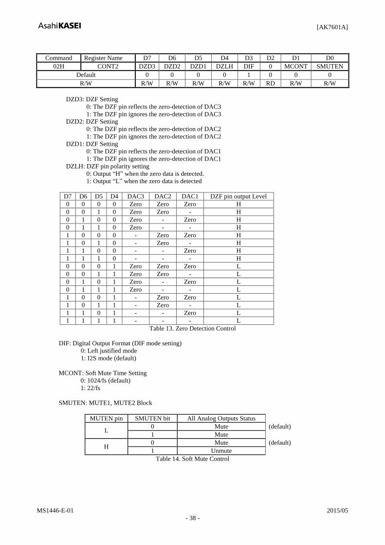
02H CONT2 DZD3 DZD2 DZD1 DZLH DIF 0 MCONT SMUTEN
Default 0 0 0 0 1 0 0 0
R/W R/W R/W R/W R/W R/W RD R/W R/W
DZD3: DZF Setting
0: The DZF pin reflects the zero-detection of DAC3
1: The DZF pin ignores the zero-detection of DAC3
DZD2: DZF Setting
0: The DZF pin reflects the zero-detection of DAC2
1: The DZF pin ignores the zero-detection of DAC2
DZD1: DZF Setting
0: The DZF pin reflects the zero-detection of DAC1
1: The DZF pin ignores the zero-detection of DAC1
DZLH: DZF pin polarity setting
0: Output “H” when the zero data is detected.
1: Output “L” when the zero data is detected
D7 D6 D5 D4 DAC3 DAC2 DAC1 DZF pin output Level
0 0 0 0 Zero Zero Zero H
0 0 1 0 Zero Zero - H
0 1 0 0 Zero - Zero H
0 1 1 0 Zero - - H
1 0 0 0 - Zero Zero H
1 0 1 0 - Zero - H
1 1 0 0 - - Zero H
1 1 1 0 - - - H
0 0 0 1 Zero Zero Zero L
0 0 1 1 Zero Zero - L
0 1 0 1 Zero - Zero L
0 1 1 1 Zero - - L
1 0 0 1 - Zero Zero L
1 0 1 1 - Zero - L
1 1 0 1 - - Zero L
1 1 1 1 - - - L
Table 13. Zero Detection Control
DIF: Digital Output Format (DIF mode setting)
0: Left justified mode
1: I2S mode (default)
MCONT: Soft Mute Time Setting
0: 1024/fs (default)
1: 22/fs
SMUTEN: MUTE1, MUTE2 Block
MUTEN pin SMUTEN bit All Analog Outputs Status
L 0 Mute (default)
1 Mute
H 0 Mute (default)
1 Unmute
Table 14. Soft Mute Control

[AK7601A]
MS1446-E-01 2015/05
- 39 -
Command Register Name D7 D6 D5 D4 D3 D2 D1 D0
03H CONT3 MOMUTE FMUTE RMUTE SWMUTE IDIF41 IDIF40 IDIF1 IDIF0
Default 0 0 0 0 1 1 1 1
R/W R/W R/W R/W R/W R/W R/W R/W R/W
MOMUTE: MOMUTE Block
0: Un-mute (default)
1: Mute (Refer to p44; DSP Block Construction)
FMUTE: FMUTE Block
0: Un-mute (default)
1: Mute (Refer to p44; DSP Block Construction)
RMUTE: RMUTE Block
0: Un-mute (default)
1: Mute (Refer to p44; DSP Block Construction)
SWMUTE: SWMUTE Block
0: Un-mute (default)
1: Mute (Refer to p44; DSP Block Construction)
IDIF41-IDIF40: Digital Input Format, IDIF Mode Setting (SDIT4)
00: 16bit LSB Justified Mode
01: 24bit LSB Justified Mode
10: 24bit MSB Justified Mode
11: 16bit/24bit I2S Mode (default)
IDIF1-IDIF0: SRC Digital Input Format, IDIF Mode Setting (SDIT1, SDTI2, SDTI3)
00: 16bit LSB Justified Mode
01: 24bit LSB Justified Mode
10: 24bit MSB Justified Mode
11: 16bit/24bit I2S Mode (default)

[AK7601A]
MS1446-E-01 2015/05
- 40 -
Command Register Name D7 D6 D5 D4 D3 D2 D1 D0
04H CONT4 LRCK BICK MCKO1 MCKO0 DO21 DO20 DO11 DO10
Default 0 0 0 0 0 0 0 0
R/W R/W R/W R/W R/W R/W R/W R/W R/W
LRCK: LRCK Output Enable
0: The OLRCK pin outputs “L”. (default)
1: The OLRCK pin outputs LRCK(1fs).
BICK: BIT Clock Output Enable
0: The OBICK pin outputs “L”. (default)
1: The OBICK pin outputs 64fs BIT clock.
MCKO1-0: Master Clock Output Enable
MCKO1 MCKO0 Master Clock Speed
0 0 “L” Output (default)
0 1 256fs (11.2896MHz)
1 0 512fs (22.5792MHz)
1 1 Reserved
Table 3. Master Clock Output Select
DO21-DO20: SDTO2/SDTI4 In/Output Enable
DO21 DO20 SDTO2/SDTI4 pin
0 0 “L” Output (default)
0 1 SDTO2
1 0 SDTI4 (Input)
1 1 Reserved
Table 15. SDTO2/SDTI4 Input/Output Select
DO11-DO10: SDTO1/SDTO3 Output Enable
DO11 DO10 SDTO1/SDTO3 pin
0 0 “L” Output (default)
0 1 SDTO1
1 0 SDTO3
1 1 Reserved
Table 16. SDTO1/SDTO3 Output Select

[AK7601A]
MS1446-E-01 2015/05
- 41 -
Command Register Name D7 D6 D5 D4 D3 D2 D1 D0
05H CONT5 0 0 0 0 SEL11 SEL10 SEL01 SEL00
Default 0 0 0 0 0 0 0 0
R/W RD RD RD RD R/W R/W R/W R/W
SEL11-10: SRC Input Selector Control
SEL11 SEL10 SRC Input
0 0 SDTI1 (default)
0 1 SDTI2
1 0 SDTI3
1 1 Reserved
Table 10. Digital Input Selector
SEL01-00: Analog Input Selector Control
SEL01 SEL00 ADC Input
0 0 AINL1/AINR1 (default)
0 1 AINL2/AINR2
1 0 AINL3/AINR3
1 1 AINL4/AINR4
Table 9. Analog Input Selector

[AK7601A]
MS1446-E-01 2015/05
- 42 -
Command Register Name D7 D6 D5 D4 D3 D2 D1 D0
06H LOUT1VOL ATT7 ATT6 ATT5 ATT4 ATT3 ATT2 ATT1 ATT0
07H ROUT1VOL ATT7 ATT6 ATT5 ATT4 ATT3 ATT2 ATT1 ATT0
08H LOUT2VOL ATT7 ATT6 ATT5 ATT4 ATT3 ATT2 ATT1 ATT0
09H ROUT2VOL ATT7 ATT6 ATT5 ATT4 ATT3 ATT2 ATT1 ATT0
0AH LOUT3VOL ATT7 ATT6 ATT5 ATT4 ATT3 ATT2 ATT1 ATT0
0BH ROUT3VOL ATT7 ATT6 ATT5 ATT4 ATT3 ATT2 ATT1 ATT0
0CH MONOLVOL ATT7 ATT6 ATT5 ATT4 ATT3 ATT2 ATT1 ATT0
0DH MONORVOL ATT7 ATT6 ATT5 ATT4 ATT3 ATT2 ATT1 ATT0
Default 0 0 0 0 0 0 0 0
R/W R/W R/W R/W R/W R/W R/W R/W R/W
ATT7-ATT0: Attenuation Level
ATT7-0 Attenuation Level
(default) 00H 0dB
01H -0.5dB
02H -1.0dB
: :
7DH -62.5dB
7EH -63.0dB
7FH -63.5dB
:
FEH -127.0dB
FFH MUTE (-∞)
Table 7. Attenuation Level

[AK7601A]
MS1446-E-01 2015/05
- 43 -
Command Register Name D7 D6 D5 D4 D3 D2 D1 D0
0EH SWCONT1 0 SW51 SW50 SW4 SW31 SW30 SW2 SW1
Default 0 0 0 0 0 1 0 0
R/W RD R/W R/W R/W R/W R/W R/W R/W
SW51-50: SDTO3, SDTI4 Selector Control
Mode SW51 SW50 Switch a Switch b Switch c Comment
Mode1 0 0 GND SDTOEQ SDTO Delay No In/Output
Mode2 0 1 SDTO EQ SDTI4 SDTO Delay In/Output before Delay
Mode3 1 0 SDTO Delay SDTOEQ SDTI4 In/Output after Delay
Mode4 1 1 - - - Reserved
Refer to Figure 33
Table 17. SDTO3/SDTI4 Selector Control
SDTI4 SDTO3
a
R1
L1
De
lay C
on
trol
c
SDTO Delay
SDTO EQ
b
Figure 31. SDTO3/SDTI4 Block Diagram
SW4: AOUT3L/R pin Output Control
0: Outputs AOUT3L/R (default)
1: Outputs AOUT2L/R
Refer to Figure 33
SW31-30: MG2 Selector Control
Refer to Figure 33
SW31 SW30 MG2 Input
0 0 SRC
0 1 ADC (default)
1 0 SDTI3
1 1 -
Table 18. MG2 Selector Control
SW2: MG1 Selector Control
0: SRC (default)
1: ADC
Refer to Figure 33
SW1: De-emphasis Control
0: Dem-OFF (default)
1: Dem-ON (44.1kHz)
Refer to Figure 33
[AK7601A]
MS1446-E-01 2015/05
- 44 -
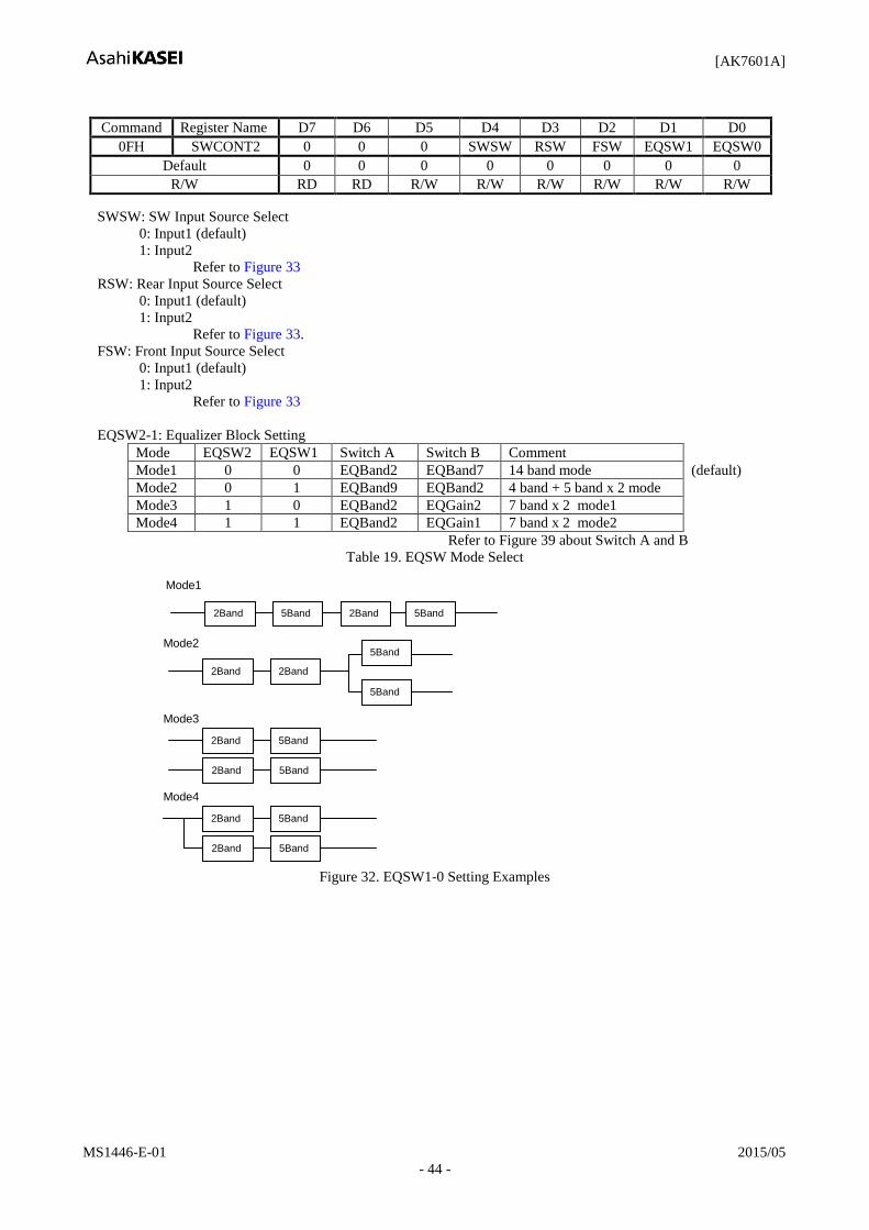
Command Register Name D7 D6 D5 D4 D3 D2 D1 D0
0FH SWCONT2 0 0 0 SWSW RSW FSW EQSW1 EQSW0
Default 0 0 0 0 0 0 0 0
R/W RD RD R/W R/W R/W R/W R/W R/W
SWSW: SW Input Source Select
0: Input1 (default)
1: Input2
Refer to Figure 33
RSW: Rear Input Source Select
0: Input1 (default)
1: Input2
Refer to Figure 33.
FSW: Front Input Source Select
0: Input1 (default)
1: Input2
Refer to Figure 33
EQSW2-1: Equalizer Block Setting
Mode EQSW2 EQSW1 Switch A Switch B Comment
Mode1 0 0 EQBand2 EQBand7 14 band mode (default)
Mode2 0 1 EQBand9 EQBand2 4 band + 5 band x 2 mode
Mode3 1 0 EQBand2 EQGain2 7 band x 2 mode1
Mode4 1 1 EQBand2 EQGain1 7 band x 2 mode2
Refer to Figure 39 about Switch A and B
Table 19. EQSW Mode Select
2Band
Mode1
5Band 2Band 5Band
2Band
Mode2
2Band
5Band
5Band
2Band
Mode3
5Band
2Band 5Band
2Band
Mode4
5Band
2Band 5Band
Figure 32. EQSW1-0 Setting Examples

[AK7601A]
MS1446-E-01 2015/05
- 45 -
Blocks and Circuits Construction of Command Setting
SR
C
Sele
cto
r
AD
C
SDTI1
SDTI2
SDTI3
AIN1L/R
De-e
mp
AIN2L/R
AIN3L/R
AIN4L/R
<<2
LG1
RG1
<<2
<<2
LG2
RG2
<<2
Fu
nctio
n1
Equaliz
er
14B
and
Fu
nctio
n2
Fu
nctio
n3
Fu
nctio
n4
Fu
nctio
n5
L1
R1
L2
R2
Dela
y
SDTO1/3
a
SDTO2/SDTI4
Xover
Xover
Xover
ADC
D-volume
MONOIN
SW4
c
b
SW3
SW2
SW1
DA
C
DA
C
DA
C
CLK MCLKO
OBICK
OLRCK
DZF
AOUT1L
AOUT1R
AOUT2L
AOUT2R
AOUT3L
AOUT3R
SDTO1
SDTO2
* set by CONT5-12(06H~0D)
MU
TE
1
MU
TE
2
Input1
Input2
MO
MU
TE
F
MU
TE
R
MU
TE
S
WM
UT
E
L1V
R1V
L2V
R2V
L3V
R3V
LMV
RMV
SDTO1 SDTO2
Spectrum Analyzer
*Refer to Figure 42 for delay block.
Figure 33. DSP Block Construction
Command 80H Shift Setting R/W Default
Data 1 (2byte) LG1 2bit Left x 4 R/W 0x 2000
Data 2 (2byte) RG1 2bit Left x 4 R/W 0x 2000
Data 3 (2byte) LG2 2bit Left x 4 R/W 0x 2000
Data 4 (2byte) RG2 2bit Left x 4 R/W 0x 2000
Data 5 (2byte) Dummy - - -

[AK7601A]
MS1446-E-01 2015/05
- 46 -
Function1 (High Frequency Expansion)
Z-1
Z-1
Z-1
Z-1
<<1 a00
a01
a02
b01
b02
Z-1
Z-1
Z-1
Z-1
<<1 a10
a11
a12
b11
b12
Z-1
Z-1
Z-1
Z-1
<<1 a00
a01
a02
b01
b02
Z-1
Z-1
Z-1
Z-1
<<1 a10
a11
a12
b11
b12
HighOut HighGainR
<<1
<<1
ThrGainR
<<1
<<1
ThrGainL
HighGainL
Lch
Rch
HiIn
HiIn
HighOut
Single Precision
Multiplier
Multiplier
Single Precision
Single Precision Single Precision
Figure 34. Function1 Block Diagram
Command 81H Shift Setting R/W Default Comment
Data 1 (2byte) ThrGainL 1bit Left x 2 R/W 0x 4000 Control register of Lch through gain
Data 2 (2byte) ThrGainR 1bit Left x 2 R/W 0x 4000 Control register of Rch through gain
Data 3 (2byte) Dummy - - -
Data 4 (2byte) Dummy - - -
Data 5 (2byte) Dummy - - -
Command 82H Shift Setting R/W Default Comment
Data 1 (2byte) HighGainL 1bit Left x 2 R/W 0x 0000 Control register of Lch IIR out gain
Data 2 (2byte) HighGainR 1bit Left x 2 R/W 0x 0000 Control register of Rch IIR out gain
Data 3 (2byte) Multiplier1 - R/W 0x 4000 Control register of Multiplier block
Data 4 (2byte) Multiplier2 - R/W 0x 0000 Control register of Multiplier block
Data 5 (2byte) Multiplier3 - R/W 0x 0000 Control register of Multiplier block
Command 84H Shift Setting R/W Default Comment
Data 1 (2byte) HiIn_a02 1bit Left x 2 R/W 0x 0000 Control register of Hi In IIR Filter
Data 2 (2byte) HiIn_a01 1bit Left x 2 R/W 0x 0000 Control register of Hi In IIR Filter
Data 3 (2byte) HiIn_a00 1bit Left x 2 R/W 0x 4000 Control register of Hi In IIR Filter
Data 4 (2byte) HiIn_b02 1bit Left x 2 R/W 0x 0000 Control register of Hi In IIR Filter
Data 5 (2byte) HiIn_b01 1bit Left x 2 R/W 0x 0000 Control register of Hi In IIR Filter
Command 85H Shift Setting R/W Default Comment
Data 1 (2byte) HiOut_a12 1bit Left x 2 R/W 0x 0000 Control register of Hi Out IIR Filter
Data 2 (2byte) HiOut_a11 1bit Left x 2 R/W 0x 0000 Control register of Hi Out IIR Filter
Data 3 (2byte) HiOut_a10 1bit Left x 2 R/W 0x 4000 Control register of Hi Out IIR Filter
Data 4 (2byte) HiOut_b12 1bit Left x 2 R/W 0x 0000 Control register of Hi Out IIR Filter
Data 5 (2byte) HiOut_b11 1bit Left x 2 R/W 0x 0000 Control register of Hi Out IIR Filter

[AK7601A]
MS1446-E-01 2015/05
- 47 -
Function2 (Compressor) Lch
Rch
LPF
Z-1
Z-1
Z-1
Z-1
<<1 a00
a01
a02
b01
b02 Double Precision
Z-1
Z-1
Z-1
Z-1
<<1 a00
a01
a02
b01
b02 Double Precision
LPF
<<1
Thr_G
Thr_G
<<1
Co
mp
resso
r
Figure 35. Function2 Block Diagram
Command C0H Shift Setting R/W Default Comment
Data 1 (4byte) LPF_a02 1bit Left x 2 R/W 0x 00000000 Control register of LPF
Data 2 (4byte) LPF_a01 1bit Left x 2 R/W 0x 00000000 Control register of LPF
Data 3 (4byte) LPF_a00 1bit Left x 2 R/W 0x 04000000 Control register of LPF
Data 4 (4byte) LPF_b02 1bit Left x 2 R/W 0x 00000000 Control register of LPF
Data 5 (4byte) LPF_b01 1bit Left x 2 R/W 0x 00000000 Control register of LPF
Command 88H Shift Setting R/W Default Comment
Data 1 (2byte) LPF_a21 1bit Left x 2 R/W 0x 0000 Control register of Compressor block
Data 2 (2byte) LPF_a20 1bit Left x 2 R/W 0x 0000 Control register of Compressor block
Data 3 (2byte) LPF_b21 1bit Left x 2 R/W 0x 0000 Control register of Compressor block
Data 4 (2byte) Dummy - - - Control register of Compressor block
Data 5 (2byte) Dummy - - - Control register of Compressor block
Command 8CH Shift Setting R/W Default Comment
Data 1 (2byte) Thr_G 1bit Left x 2 R/W 0x 4000 Control register of through gain
Data 2 (2byte) Dummy - - -
Data 3 (2byte) Dummy - - -
Data 4 (2byte) Dummy - - -
Data 5 (2byte) Dummy - - -
Command 8DH Shift Setting R/W Default Comment
Data 1 (2byte) Compressor1 - R/W 0x 0000 Control register of Compressor block
Data 2 (2byte) Compressor2 - R/W 0x 0000 Control register of Compressor block
Data 3 (2byte) Compressor3 - R/W 0x 0000 Control register of Compressor block
Data 4 (2byte) Compressor4 - R/W 0x 0000 Control register of Compressor block
Data 5 (2byte) Dummy - - -

[AK7601A]
MS1446-E-01 2015/05
- 48 -
Function3 (Surround Effect)
Z-1
Z-1
Z-1
Z-1
<<1 a00
a01
a02
b01
b02 Single Precision
Z-n
F3ThrG
F3OutR
F3OutL
F3ThrG
Lch
Rch
F3InR
F3InL
F3FBG
F3D
Max0x2D Sample
F3IIR
<<1
<<1
Figure 36. Function3 Block Diagram
Command 90H Shift Setting R/W Default Comment
Data 1 (2byte) F3ThrG 1bit Left x 2 R/W 0x 4000 Control register of through gain
Data 2 (2byte) F3OutL 1bit Left x 2 R/W 0x 0000 Control register of Lch F3 IIR out gain
Data 3 (2byte) F3OutR 1bit Left x 2 R/W 0x 0000 Control register of Rch F3 IIR out gain
Data 4 (2byte) Dummy - - -
Data 5 (2byte) Dummy - - -
Command 91H Shift Setting R/W Default Comment
Data 1 (2byte) F3InL - R/W 0x 0000
Data 2 (2byte) F3InR - R/W 0x 0000
Data 3 (2byte) F3D - R/W 0x 0000
Data 4 (2byte) F3FBG - R/W 0x 0000
Data 5 (2byte) Dummy - - -
Command 92H Shift Setting R/W Default Comment
Data 1 (2byte) F3IIR_a02 1bit Left x 2 R/W 0x 0000
Data 2 (2byte) F3IIR_a01 1bit Left x 2 R/W 0x 0000
Data 3 (2byte) F3IIR_a00 1bit Left x 2 R/W 0x 4000
Data 4 (2byte) F3IIR_b02 1bit Left x 2 R/W 0x 0000
Data 5 (2byte) F3IIR_b01 1bit Left x 2 R/W 0x 0000
[AK7601A]
MS1446-E-01 2015/05
- 49 -
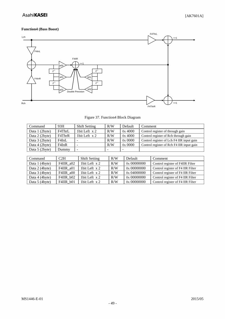
Function4 (Bass Boost)
Z-1
Z-1
Z-1
Z-1
<<1 a00
a01
a02
b01
b02 Double Precision
F4ThrR
F4ThrL
Lch
Rch
F4InR
F4InL
F4IIR
<<1
<<1
Figure 37. Function4 Block Diagram
Command 93H Shift Setting R/W Default Comment
Data 1 (2byte) F4ThrL 1bit Left x 2 R/W 0x 4000 Control register of through gain
Data 2 (2byte) F4ThrR 1bit Left x 2 R/W 0x 4000 Control register of Rch through gain
Data 3 (2byte) F4InL - R/W 0x 0000 Control register of Lch F4 IIR input gain
Data 4 (2byte) F4InR - R/W 0x 0000 Control register of Rch F4 IIR input gain
Data 5 (2byte) Dummy - - -
Command C2H Shift Setting R/W Default Comment
Data 1 (4byte) F4IIR_a02 1bit Left x 2 R/W 0x 00000000 Control register of F4IIR Filter
Data 2 (4byte) F4IIR_a01 1bit Left x 2 R/W 0x 00000000 Control register of F4 IIR Filter
Data 3 (4byte) F4IIR_a00 1bit Left x 2 R/W 0x 04000000 Control register of F4 IIR Filter
Data 4 (4byte) F4IIR_b02 1bit Left x 2 R/W 0x 00000000 Control register of F4 IIR Filter
Data 5 (4byte) F4IIR_b01 1bit Left x 2 R/W 0x 00000000 Control register of F4 IIR Filter

[AK7601A]
MS1446-E-01 2015/05
- 50 -
Function5 (Loudness)
Z-1
Z-1
Z-1
Z-1
<<1 a00
a01
a02
b01
b02 Single Precision
F5OutG
F5ThrG
Lch
Rch
F3IIR
<<1
<<1
Z-1
Z-1
Z-1
Z-1
<<1 a00
a01
a02
b01
b02 Single Precision
F5IIR
F5IIR
F5ThrG
F5OutG
Figure 38. Function5 Block Diagram
Command 94H Shift Setting R/W Default Comment
Data 1 (2byte) F5ThrG 1bit Left x 2 R/W 0x 4000 Control register of through gain
Data 2 (2byte) F5OutG 1bit Left x 2 R/W 0x 0000 Control register of F5 IIR out gain
Data 3 (2byte) Dummy - - -
Data 4 (2byte) Dummy - - -
Data 5 (2byte) Dummy - - -
Command 95H Shift Setting R/W Default Comment
Data 1 (2byte) F5IIR_a02 1bit Left x 2 R/W 0x 0000 Control register of F5 IIR Filter
Data 2 (2byte) F5IIR_a01 1bit Left x 2 R/W 0x 0000 Control register of F5 IIR Filter
Data 3 (2byte) F5IIR_a00 1bit Left x 2 R/W 0x 4000 Control register of F5 IIR Filter
Data 4 (2byte) F5IIR_b02 1bit Left x 2 R/W 0x 0000 Control register of F5 IIR Filter
Data 5 (2byte) F5IIR_b01 1bit Left x 2 R/W 0x 0000 Control register of F5 IIR Filter
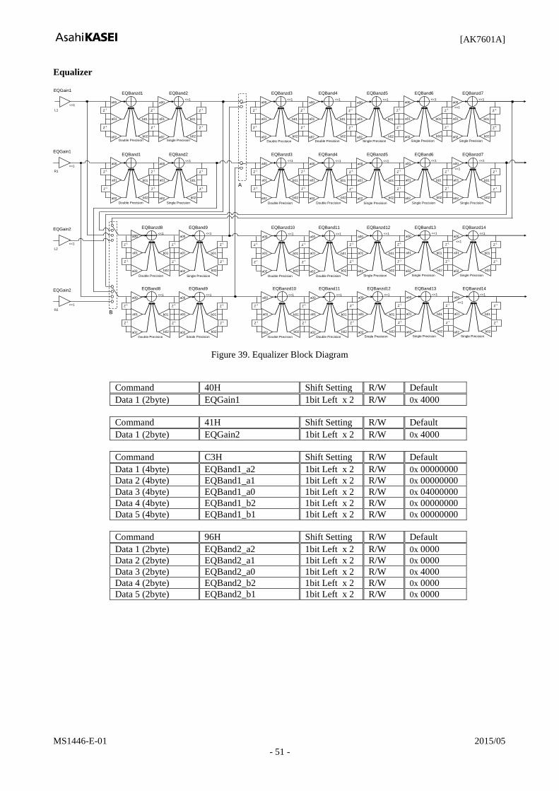
[AK7601A]
MS1446-E-01 2015/05
- 51 -
Equalizer
EQGain1
L1
Z-1
<<1 a00
a01
a02
b01
b02
Z-1
Z-1
<<1 a00
a01
a02
b01
b02
Z-1
Z-1
<<1 a00
a01
a02
b01
b02
Z-1
Z-1
<<1 a00
a01
a02
b01
b02
Z-1
Z-1
<<1 a00
a01
a02
b01
b02
Z-1
Z-1
Z-1
Z-1
<<1 a00
a01
a02
b01
b02
Z-1
Z-1
<<1 a00
a01
a02
b01
b02
Z-1
Z-1
<<1 a00
a01
a02
b01
b02
Z-1
Z-1
<<1 a00
a01
a02
b01
b02
Z-1
Z-1
<<1 a00
a01
a02
b01
b02
Z-1
Z-1
Z-1
Z-1
<<1 a00
a01
a02
b01
b02
Z-1
Z-1
<<1 a00
a01
a02
b01
b02
Z-1
Z-1
<<1 a00
a01
a02
b01
b02
Z-1
Z-1
<<1 a00
a01
a02
b01
b02
Z-1
Z-1
<<1 a00
a01
a02
b01
b02
Z-1
Z-1
Z-1
<<1
EQGain1
R1
<<1
Z-1
<<1 a00
a01
a02
b01
b02
Z-1
Z-1
<<1 a00
a01
a02
b01
b02
Z-1
Z-1
Z-1
Z-1
<<1 a00
a01
a02
b01
b02
Z-1
Z-1
<<1 a00
a01
a02
b01
b02
Z-1
Z-1
Z-1
Z-1
a00
a01
a02
b01
b02
Z-1
Z-1
<<1 a00
a01
a02
b01
b02
Z-1
Z-1
Z-1
Z-1
a00
a01
a02
b01
b02
Double Precision
Z-1
Z-1
<<1 a00
a01
a02
b01
b02
Single Precision
Z-1
Z-1
Z-1
Z-1
<<1 a00
a01
a02
b01
b02
Z-1
Z-1
<<1 a00
a01
a02
b01
b02
Z-1
Z-1
<<1 a00
a01
a02
b01
b02
Z-1
Z-1
<<1 a00
a01
a02
b01
b02
Z-1
Z-1
<<1 a00
a01
a02
b01
b02
Z-1
Z-1
Z-1
A
EQGain2
L2
<<1
EQGain2
R2
<<1
B
EQBanzd1 EQBand2
EQBand1 EQBand2
EQBanzd8 EQBand9
EQBand8 EQBand9
EQBanzd3 EQBand4 EQBanzd5 EQBand6 EQBanzd7
EQBanzd3 EQBand4 EQBanzd5 EQBand6 EQBanzd7
EQBanzd10 EQBand11 EQBanzd12 EQBand13 EQBanzd14
EQBanzd10 EQBand11 EQBanzd12 EQBand13 EQBanzd14
<<1
<<1
<<1
<<1
Double Precision Single Precision
Double Precision Single Precision
Double Precision Single Precision Double Precision Double Precision
Double Precision Double Precision
Double Precision Double Precision
Double Precision Double Precision
Single Precision Single Precision Single Precision
Single Precision Single Precision Single Precision
Single Precision Single Precision Single Precision
Single Precision Single Precision Single Precision
Figure 39. Equalizer Block Diagram
Command 40H Shift Setting R/W Default
Data 1 (2byte) EQGain1 1bit Left x 2 R/W 0x 4000
Command 41H Shift Setting R/W Default
Data 1 (2byte) EQGain2 1bit Left x 2 R/W 0x 4000
Command C3H Shift Setting R/W Default
Data 1 (4byte) EQBand1_a2 1bit Left x 2 R/W 0x 00000000
Data 2 (4byte) EQBand1_a1 1bit Left x 2 R/W 0x 00000000
Data 3 (4byte) EQBand1_a0 1bit Left x 2 R/W 0x 04000000
Data 4 (4byte) EQBand1_b2 1bit Left x 2 R/W 0x 00000000
Data 5 (4byte) EQBand1_b1 1bit Left x 2 R/W 0x 00000000
Command 96H Shift Setting R/W Default
Data 1 (2byte) EQBand2_a2 1bit Left x 2 R/W 0x 0000
Data 2 (2byte) EQBand2_a1 1bit Left x 2 R/W 0x 0000
Data 3 (2byte) EQBand2_a0 1bit Left x 2 R/W 0x 4000
Data 4 (2byte) EQBand2_b2 1bit Left x 2 R/W 0x 0000
Data 5 (2byte) EQBand2_b1 1bit Left x 2 R/W 0x 0000
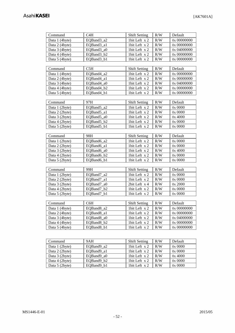
[AK7601A]
MS1446-E-01 2015/05
- 52 -
Command C4H Shift Setting R/W Default
Data 1 (4byte) EQBand3_a2 1bit Left x 2 R/W 0x 00000000
Data 2 (4byte) EQBand3_a1 1bit Left x 2 R/W 0x 00000000
Data 3 (4byte) EQBand3_a0 1bit Left x 2 R/W 0x 04000000
Data 4 (4byte) EQBand3_b2 1bit Left x 2 R/W 0x 00000000
Data 5 (4byte) EQBand3_b1 1bit Left x 2 R/W 0x 00000000
Command C5H Shift Setting R/W Default
Data 1 (4byte) EQBand4_a2 1bit Left x 2 R/W 0x 00000000
Data 2 (4byte) EQBand4_a1 1bit Left x 2 R/W 0x 00000000
Data 3 (4byte) EQBand4_a0 1bit Left x 2 R/W 0x 04000000
Data 4 (4byte) EQBand4_b2 1bit Left x 2 R/W 0x 00000000
Data 5 (4byte) EQBand4_b1 1bit Left x 2 R/W 0x 00000000
Command 97H Shift Setting R/W Default
Data 1 (2byte) EQBand5_a2 1bit Left x 2 R/W 0x 0000
Data 2 (2byte) EQBand5_a1 1bit Left x 2 R/W 0x 0000
Data 3 (2byte) EQBand5_a0 1bit Left x 2 R/W 0x 4000
Data 4 (2byte) EQBand5_b2 1bit Left x 2 R/W 0x 0000
Data 5 (2byte) EQBand5_b1 1bit Left x 2 R/W 0x 0000
Command 98H Shift Setting R/W Default
Data 1 (2byte) EQBand6_a2 1bit Left x 2 R/W 0x 0000
Data 2 (2byte) EQBand6_a1 1bit Left x 2 R/W 0x 0000
Data 3 (2byte) EQBand6_a0 1bit Left x 2 R/W 0x 4000
Data 4 (2byte) EQBand6_b2 1bit Left x 2 R/W 0x 0000
Data 5 (2byte) EQBand6_b1 1bit Left x 2 R/W 0x 0000
Command 99H Shift Setting R/W Default
Data 1 (2byte) EQBand7_a2 1bit Left x 2 R/W 0x 0000
Data 2 (2byte) EQBand7_a1 1bit Left x 2 R/W 0x 0000
Data 3 (2byte) EQBand7_a0 2bit Left x 4 R/W 0x 2000
Data 4 (2byte) EQBand7_b2 1bit Left x 2 R/W 0x 0000
Data 5 (2byte) EQBand7_b1 1bit Left x 2 R/W 0x 0000
Command C6H Shift Setting R/W Default
Data 1 (4byte) EQBand8_a2 1bit Left x 2 R/W 0x 00000000
Data 2 (4byte) EQBand8_a1 1bit Left x 2 R/W 0x 00000000
Data 3 (4byte) EQBand8_a0 1bit Left x 2 R/W 0x 04000000
Data 4 (4byte) EQBand8_b2 1bit Left x 2 R/W 0x 00000000
Data 5 (4byte) EQBand8_b1 1bit Left x 2 R/W 0x 00000000
Command 9AH Shift Setting R/W Default
Data 1 (2byte) EQBand9_a2 1bit Left x 2 R/W 0x 0000
Data 2 (2byte) EQBand9_a1 1bit Left x 2 R/W 0x 0000
Data 3 (2byte) EQBand9_a0 1bit Left x 2 R/W 0x 4000
Data 4 (2byte) EQBand9_b2 1bit Left x 2 R/W 0x 0000
Data 5 (2byte) EQBand9_b1 1bit Left x 2 R/W 0x 0000

[AK7601A]
MS1446-E-01 2015/05
- 53 -
Command C7H Shift Setting R/W Default
Data 1 (4byte) EQBand10_a2 1bit Left x 2 R/W 0x 00000000
Data 2 (4byte) EQBand10_a1 1bit Left x 2 R/W 0x 00000000
Data 3 (4byte) EQBand10_a0 1bit Left x 2 R/W 0x 04000000
Data 4 (4byte) EQBand10_b2 1bit Left x 2 R/W 0x 00000000
Data 5 (4byte) EQBand10_b1 1bit Left x 2 R/W 0x 00000000
Command C8H Shift Setting R/W Default
Data 1 (4byte) EQBand11_a2 1bit Left x 2 R/W 0x 00000000
Data 2 (4byte) EQBand11_a1 1bit Left x 2 R/W 0x 00000000
Data 3 (4byte) EQBand11_a0 1bit Left x 2 R/W 0x 04000000
Data 4 (4byte) EQBand11_b2 1bit Left x 2 R/W 0x 00000000
Data 5 (4byte) EQBand11_b1 1bit Left x 2 R/W 0x 00000000
Command 9BH Shift Setting R/W Default
Data 1 (2byte) EQBand12_a2 1bit Left x 2 R/W 0x 0000
Data 2 (2byte) EQBand12_a1 1bit Left x 2 R/W 0x 0000
Data 3 (2byte) EQBand12_a0 1bit Left x 2 R/W 0x 4000
Data 4 (2byte) EQBand12_b2 1bit Left x 2 R/W 0x 0000
Data 5 (2byte) EQBand12_b1 1bit Left x 2 R/W 0x 0000
Command 9CH Shift Setting R/W Default
Data 1 (2byte) EQBand13_a2 1bit Left x 2 R/W 0x 0000
Data 2 (2byte) EQBand13_a1 1bit Left x 2 R/W 0x 0000
Data 3 (2byte) EQBand13_a0 1bit Left x 2 R/W 0x 4000
Data 4 (2byte) EQBand13_b2 1bit Left x 2 R/W 0x 0000
Data 5 (2byte) EQBand13_b1 1bit Left x 2 R/W 0x 0000
Command 9DH Shift Setting R/W Default
Data 1 (2byte) EQBand14_a2 1bit Left x 2 R/W 0x 0000
Data 2 (2byte) EQBand14_a1 1bit Left x 2 R/W 0x 0000
Data 3 (2byte) EQBand14_a0 2bit Left x 4 R/W 0x 2000
Data 4 (2byte) EQBand14_b2 1bit Left x 2 R/W 0x 0000
Data 5 (2byte) EQBand14_b1 1bit Left x 2 R/W 0x 0000

[AK7601A]
MS1446-E-01 2015/05
- 54 -
Cross Over
FOutGain
RL
<<1
XO2IIR
RR
<<1
Z-1
<<1 a00
a01
a02
b01
b02
Z-1
Z-1
<<1 a10
a11
a12
b11
b12
Z-1
Z-1
Z-1
Z-1
<<1 a00
a01
a02
b01
b02
Z-1
Z-1
<<1 a10
a11
a12
b11
b12
Z-1
Z-1
Z-1
Z-1
<<1 a00
a01
a02
b01
b02
Z-1
Z-1
<<1 a10
a11
a12
b11
b12
Z-1
Z-1
<<1 a20
a21
a22
b21
b22
Z-1
Z-1
Z-1
Z-1
<<1 a00
a01
a02
b01
b02
Double Precision
Z-1
Z-1
<<1 a10
a11
a12
b11
b12
Z-1
Z-1
<<1 a20
a21
a22
b21
b22
Single Precision
Z-1
Z-1
Z-1
<<1
<<1
FOutGain
ROutGain
ROutGain
FL
FR
XO2IIR
XO2IIR XO2IIR
XO1IIR XO1IIR XO1IIR
XO1IIR XO1IIR XO1IIR
XO3IIR XO3IIR
a00 ~ c02 a10 ~ b12 SWOutGain
SWL
SWR
Double Precision
Double Precision Double Precision
Double Precision Double Precision
Double Precision Double Precision
Double Precision Double Precision
Single Precision
Figure 40. Cross Over Block Diagram
Command 42H Shift Setting R/W Default
Data 1 (2byte) Fout Gain 1bit Left x 2 R/W 0x 4000
Command 43H Shift Setting R/W Default
Data 1 (2byte) Rout Gain 1bit Left x 2 R/W 0x 4000
Command 44H Shift Setting R/W Default
Data 1 (2byte) SWout Gain 1bit Left x 2 R/W 0x 4000
Command C9H Shift Setting R/W Default
Data 1 (4byte) XO1IIR_a02 1bit Left x 2 R/W 0x 00000000
Data 2 (4byte) XO1IIR_a01 1bit Left x 2 R/W 0x 00000000
Data 3 (4byte) XO1IIR_a00 1bit Left x 2 R/W 0x 04000000
Data 4 (4byte) XO1IIR_b02 1bit Left x 2 R/W 0x 00000000
Data 5 (4byte) XO1IIR_b01 1bit Left x 2 R/W 0x 00000000

[AK7601A]
MS1446-E-01 2015/05
- 55 -
Command CAH Shift Setting R/W Default
Data 1 (4byte) XO2IIR_a02 1bit Left x 2 R/W 0x 00000000
Data 2 (4byte) XO2IIR_a01 1bit Left x 2 R/W 0x 00000000
Data 3 (4byte) XO2IIR_a00 1bit Left x 2 R/W 0x 04000000
Data 4 (4byte) XO2IIR_b02 1bit Left x 2 R/W 0x 00000000
Data 5 (4byte) XO2IIR_b01 1bit Left x 2 R/W 0x 00000000
Command CBH Shift Setting R/W Default
Data 1 (4byte) XO3IIR_a02 1bit Left x 2 R/W 0x 00000000
Data 2 (4byte) XO3IIR_a01 1bit Left x 2 R/W 0x 00000000
Data 3 (4byte) XO3IIR_a00 1bit Left x 2 R/W 0x 04000000
Data 4 (4byte) XO3IIR_b02 1bit Left x 2 R/W 0x 00000000
Data 5 (4byte) XO3IIR_b01 1bit Left x 2 R/W 0x 00000000
Command CCH Shift Setting R/W Default
Data 1 (4byte) XO1IIR_a12 1bit Left x 2 R/W 0x 00000000
Data 2 (4byte) XO1IIR_a11 1bit Left x 2 R/W 0x 00000000
Data 3 (4byte) XO1IIR_a10 1bit Left x 2 R/W 0x 04000000
Data 4 (4byte) XO1IIR_b12 1bit Left x 2 R/W 0x 00000000
Data 5 (4byte) XO1IIR_b11 1bit Left x 2 R/W 0x 00000000
Command CDH Shift Setting R/W Default
Data 1 (4byte) XO2IIR_a12 1bit Left x 2 R/W 0x 00000000
Data 2 (4byte) XO2IIR_a11 1bit Left x 2 R/W 0x 00000000
Data 3 (4byte) XO2IIR_a10 1bit Left x 2 R/W 0x 04000000
Data 4 (4byte) XO2IIR_b12 1bit Left x 2 R/W 0x 00000000
Data 5 (4byte) XO2IIR_b11 1bit Left x 2 R/W 0x 00000000
Command CEH Shift Setting R/W Default
Data 1 (4byte) XO3IIR_a12 1bit Left x 2 R/W 0x 00000000
Data 2 (4byte) XO3IIR_a11 1bit Left x 2 R/W 0x 00000000
Data 3 (4byte) XO3IIR_a10 1bit Left x 2 R/W 0x 04000000
Data 4 (4byte) XO3IIR_b12 1bit Left x 2 R/W 0x 00000000
Data 5 (4byte) XO3IIR_b11 1bit Left x 2 R/W 0x 00000000
Command 9EH Shift Setting R/W Default
Data 1 (2byte) XO1IIR_a22 1bit Left x 2 R/W 0x 0000
Data 2 (2byte) XO1IIR_a21 1bit Left x 2 R/W 0x 0000
Data 3 (2byte) XO1IIR_a20 1bit Left x 2 R/W 0x 4000
Data 4 (2byte) XO1IIR_b22 1bit Left x 2 R/W 0x 0000
Data 5 (2byte) XO1IIR_b21 1bit Left x 2 R/W 0x 0000

[AK7601A]
MS1446-E-01 2015/05
- 56 -
Spectrum Analyzer
Z-1
<<1 a00
a02
b01
b02
Double Precision
Z-1
Z-1
Z-1
SAIIR1
SAIIR4
a30 ~ c32 a50 ~ b52
SAIIR3
a20 ~ c22 a50 ~ b52
SAIIR2 a10 ~ c12 a50 ~ b52
a50
a51 b51
Z-1
Z-1
SASIIR
Resister | X | >>3 Lch
Rch
Double Precision Double Precision
Double Precision
Double Precision
Double Precision
Single Precision
Single Precision
Figure 41. Spectrum Analyzer Block Diagram
Command CFH Shift Setting R/W Default
Data 1 (4byte) SAIIR1_a02 1bit Left x 2 R/W 0x 0FFE2D4D
Data 2 (4byte) SAIIR1_a00 1bit Left x 2 R/W 0x 0001D2B3
Data 3 (4byte) SAIIR1_b02 1bit Left x 2 R/W 0x 0C009B92
Data 4 (4byte) SAIIR1_b01 1bit Left x 2 R/W 0x 07FF1150
Data 5 (4byte) Dummy - - -
Command D0H Shift Setting R/W Default
Data 1 (4byte) SAIIR2_a02 1bit Left x 2 R/W 0x 0FF51627
Data 2 (4byte) SAIIR2_a00 1bit Left x 2 R/W 0x 000AE9D9
Data 3 (4byte) SAIIR2_b02 1bit Left x 2 R/W 0x 0C03A349
Data 4 (4byte) SAIIR2_b01 1bit Left x 2 R/W 0x 07F72D4D
Data 5 (4byte) Dummy - - -
Command D1H Shift Setting R/W Default
Data 1 (4byte) SASIIR_a51 - R/W 0x 00031773
Data 2 (4byte) SASIIR_a50 - R/W 0x 00031773
Data 3 (4byte) SASIIR_b51 - R/W 0x 07FBA0B8
Data 4 (4byte) Dummy - - -
Data 5 (4byte) Dummy - - -
Command 9FH Shift Setting R/W Default
Data 1 (2byte) SAIIR3_a22 1bit Left x 2 R/W 0x FD52
Data 2 (2byte) SAIIR3_a20 1bit Left x 2 R/W 0x 02AE
Data 3 (2byte) SAIIR3_b22 1bit Left x 2 R/W 0x C0E5
Data 4 (2byte) SAIIR3_b21 1bit Left x 2 R/W 0x 79FB
Data 5 (2byte) Dummy - - -
Command A0H Shift Setting R/W Default
Data 1 (2byte) SAIIR4_a32 1bit Left x 2 R/W 0x F779
Data 2 (2byte) SAIIR4_a30 1bit Left x 2 R/W 0x 0887
Data 3 (2byte) SAIIR4_b32 1bit Left x 2 R/W 0x C2D8
Data 4 (2byte) SAIIR4_b31 1bit Left x 2 R/W 0x 3449
Data 5 (2byte) Dummy - - -
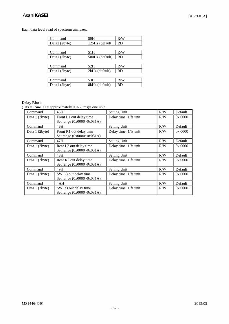
[AK7601A]
MS1446-E-01 2015/05
- 57 -
Each data level read of spectrum analyzer.
Command 50H R/W
Data1 (2byte) 125Hz (default) RD
Command 51H R/W
Data1 (2byte) 500Hz (default) RD
Command 52H R/W
Data1 (2byte) 2kHz (default) RD
Command 53H R/W
Data1 (2byte) 8kHz (default) RD
Delay Block
(1/fs = 1/44100 = approximately 0.0226ms)= one unit
Command 45H Setting Unit R/W Default
Data 1 (2byte) Front L1 out delay time
Set range (0x0000~0x031A)
Delay time: 1/fs unit R/W 0x 0000
Command 46H Setting Unit R/W Default
Data 1 (2byte) Front R1 out delay time
Set range (0x0000~0x031A)
Delay time: 1/fs unit R/W 0x 0000
Command 47H Setting Unit R/W Default
Data 1 (2byte) Rear L2 out delay time
Set range (0x0000~0x031A)
Delay time: 1/fs unit R/W 0x 0000
Command 48H Setting Unit R/W Default
Data 1 (2byte) Rear R2 out delay time
Set range (0x0000~0x031A)
Delay time: 1/fs unit R/W 0x 0000
Command 49H Setting Unit R/W Default
Data 1 (2byte) SW L3 out delay time
Set range (0x0000~0x031A)
Delay time: 1/fs unit R/W 0x 0000
Command 4AH Setting Unit R/W Default
Data 1 (2byte) SW R3 out delay time
Set range (0x0000~0x031A)
Delay time: 1/fs unit R/W 0x 0000

[AK7601A]
MS1446-E-01 2015/05
- 58 -
Command A1H Shift Setting R/W Default
Data 1 (2byte) Front L Gain Setting Coefficient 1bit Left x2 R/W 0x 4000
Data 1 (2byte) Front R Gain Setting Coefficient 1bit Left x2 R/W 0x 4000
Data 1 (2byte) Rear L Gain Setting Coefficient 1bit Left x2 R/W 0x 4000
Data 1 (2byte) Rear R Gain Setting Coefficient 1bit Left x2 R/W 0x 4000
Data 1 (2byte) Dummy - - -
Command A2H Shift Setting R/W Default
Data 1 (2byte) SW L Gain Setting Coefficient 1bit Left x2 R/W 0x 4000
Data 1 (2byte) SW R Gain Setting Coefficient 1bit Left x2 R/W 0x 4000
Data 1 (2byte) Dummy - - -
Data 1 (2byte) Dummy - - -
Data 1 (2byte) Dummy - - -
Note: All data are R/W.
When the delay time is set over its limit, it will be set to the maximum value.
<Delay Amount Setting Example>
SWSW, RSW and FSW bits in 0FH control input source setting.
Example1. Input1 → L1, L2, L3
Input2 → No data
Delay Memory 1word=24bit
18ms Delay = 794word (44.1kHz x 0.018)
FL RL
NL
L1 out (Front)
L2 out (Rear)
L3 out (SW)
Lch in
put
1
<< 1
<< 1
<< 1
Example2. Input1 →L2, L3
Input2 → L1
Delay Memory 1word=24bit
18ms Delay = 794word (44.1kHz x 0.018)
FL RL
NL
L1 out (Front)
L2 out (Rear)
L3 out (SW)
Lch input 1
<< 1
<< 1
<< 1
Lch input 2
Figure 42. Delay Amount Setting Example

[AK7601A]
MS1446-E-01 2015/05
- 59 -
SYSTEM DESIGN
Figure 43 shows system connection diagram. An evaluation board (AKD7601A) is available for fast evaluation as well as
suggestions for peripheral circuitry.
0.1u
μP
0.1u
XT
O
MUTEN 37
38
39
40
41
42
43
44
45
47
46
VSS3
REF18
VSS4
MONOIN
AINL1
GNDIN1
AINR1
AINL2
GNDIN2
SDTO1/SDTO3
XT
I
ILR
CK
1
IBIC
K1
IBIC
K2
IBIC
K3
SD
TI1
SD
TI3
AIN
L3
VSS2
1
2
3
4
5
6
7
8
9
10
11 A
INR
4
AIN
R3
AIN
L4
VC
OM
VS
S1
VR
EF
H
AO
UT
1L
AO
UT
1R
AO
UT
2L
SDTO2/SDTI4
OLRCK
OBICK
MCKO
SCL
SDA
PDN
DZF
AOUT3R
AK7601AVQ
AV
DD
ILR
CK
2
ILR
CK
3
CLKMODE
24
23
22
21
20
19
18
17
16
14
15
36
35
34
33
32
31
30
29
28
27
26
48 AINR2
12 A
OU
T2
R
AOUT3L 13
DV
DD
25
SD
TI2
Top View
0.1u
2.2u
0.1u
0.1u
MUTEN
Digital 5V
2.2u
10u
Mute
Mute
Mute
Mute
Mute
Mute
DSP4
10u
Analog 5V
10u
DSP1 DSP2 DSP3
Digital Ground
Analog Ground
Figure 43. System Connection Diagram
• X’tal mode (CLKMODE pin = “L”)
• SDTO3, SDTI4 Select Mode (DO21-20 bits = “10”, DO11-10 bits = “10”)
Note: Do not take current from the REF18 pin.

[AK7601A]
MS1446-E-01 2015/05
- 60 -
1. Grounding and Power Supply Decoupling
The AK7601A requires careful attention to power supply and grounding arrangements. AVDD and DVDD are usually
supplied from the system’s analog supply. If AVDD and DVDD are supplied separately, AVDD must be ON after DVDD
is ON. VSS1, VSS2, VSS3 and VSS4 of the AK7601A should be connected to the analog ground plane. System
analog ground and digital ground should be connected together near to where the supplies are brought onto the printed
circuit board. Decoupling capacitors should be as near to the AK7601A as possible, with the small value ceramic
capacitor being the nearest.
2. Voltage Reference Inputs
The input voltage to the VREFH pin sets the analog output range. Usually the VREFH pin is connected to the AVDD pin
and a 0.1F ceramic capacitor is connected between the AVDD pin and the VSS1 pin. VCOM is a signal ground of this
chip (AVDD/2). The electrolytic capacitor around 2.2µF attached between the VCOM pin an the VSS1 pin eliminates the
effects of high frequency noise. The ceramic capacitor in particular should be connected as close as possible to the pin. No
load current may be taken from the VCOM pin. All signals, especially clock, should be kept away from the VREFH pin
and the VCOM pin in order to avoid unwanted coupling into the AK7601A.
3. Analog Inputs The ADC supports single-ended and pseudo-differential inputs. It is biased to VCOM voltage (AVDD/2) internally by
45kΩ(typ). The inputs signal range scales with nominally at 0.65 x VREFH Vpp (typ). The AK7601A can accept input
voltage from VSS1 to AVDD. The output code format is 2's complement. Input DC offset is canceled by an integrated
high-pass filter.
The AK7601A samples the analog input at 64fs. A digital filter removes the noise over the stopband attenuation level,
except for a band of integral multiplication of 64fs. AK7601A has an integrated anti-alias RC filter in order to reduce the
noise at 64fs.
4. Analog output The DAC output is single-ended and output range is 0.65xVREFH Vpp (typ) centered on VCOM. The bias voltage of the
external summing circuit is supplied externally. The input data format is two’s compliment. Positive full-scale output
corresponds to 7FFFFFH (@24bit) input code, Negative full scale is 800000H (@24bit) and VCOM voltage ideally is
000000H (@24bit). The Out-of-Band noise (shaping noise) generated by the internal delta-sigma modulator is attenuated
by an integrated switched capacitor filter (SCF) and a continuous time filter (CTF).
DC offsets on analog outputs are eliminated by AC coupling since analog outputs has DC offset of VCOM.
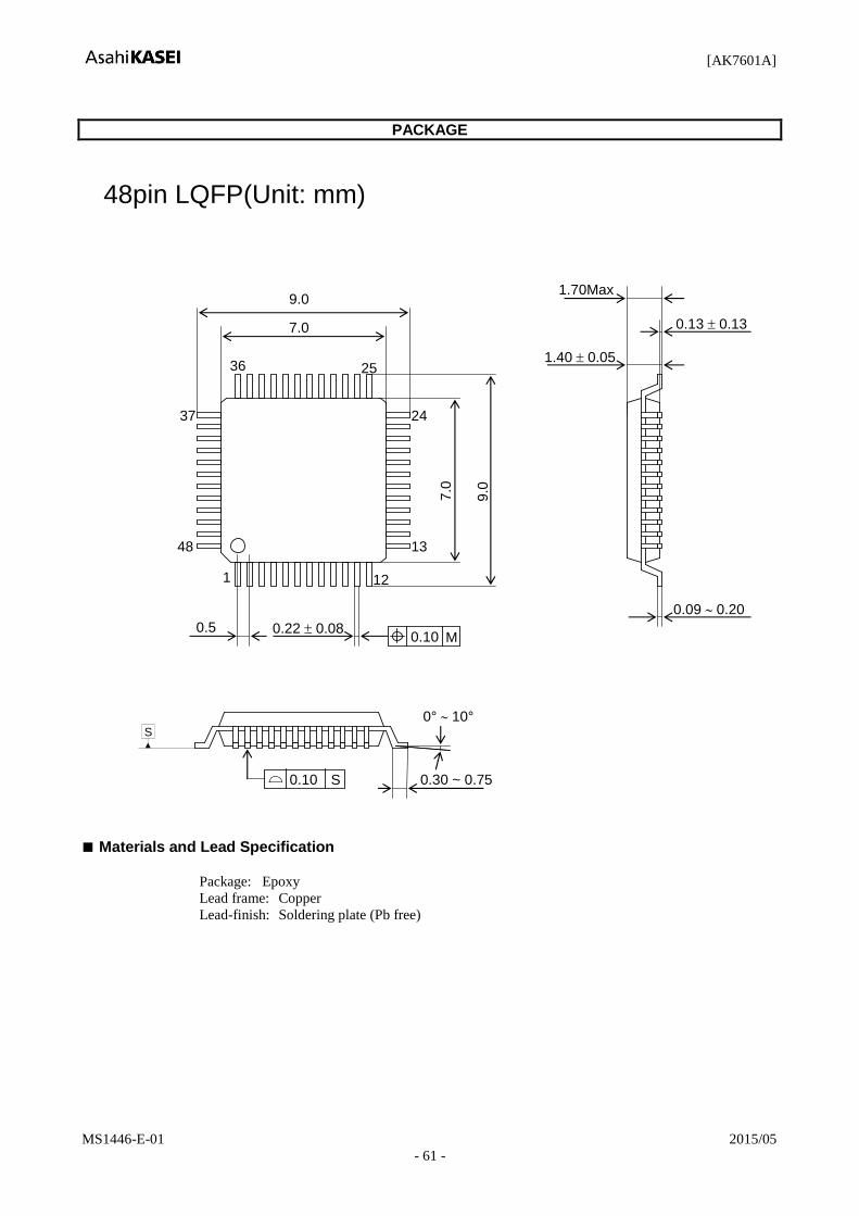
[AK7601A]
MS1446-E-01 2015/05
- 61 -
PACKAGE
1 12
48
13
7.0 9.0
7.0
9.0
0.22 0.08
48pin LQFP(Unit: mm)
0.10
37 24
25 36
0.09 0.20
1.40 0.05
0.13 0.13
1.70Max
0° 10°
0.10
0.30 ~ 0.75
0.5
S
S
M
Materials and Lead Specification
Package: Epoxy
Lead frame: Copper
Lead-finish: Soldering plate (Pb free)
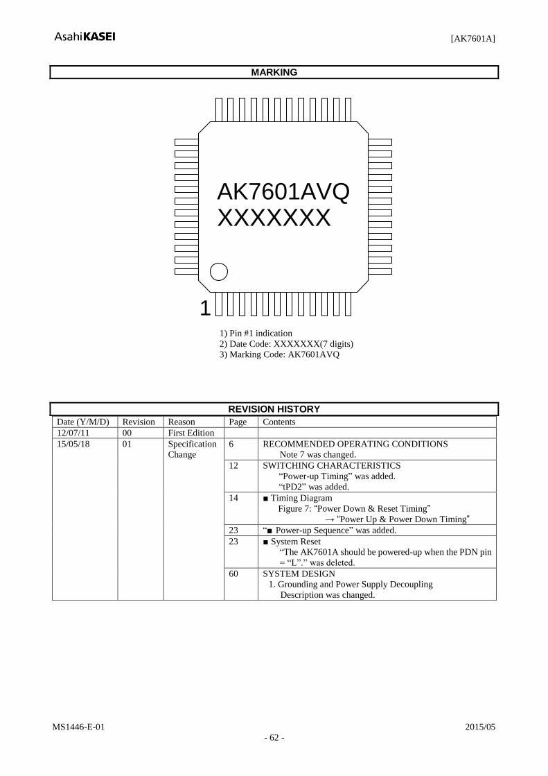
[AK7601A]
MS1446-E-01 2015/05
- 62 -
MARKING
AK7601AVQ XXXXXXX
1
1) Pin #1 indication
2) Date Code: XXXXXXX(7 digits)
3) Marking Code: AK7601AVQ
REVISION HISTORY
Date (Y/M/D) Revision Reason Page Contents
12/07/11 00 First Edition
15/05/18 01 Specification
Change
6 RECOMMENDED OPERATING CONDITIONS
Note 7 was changed.
12 SWITCHING CHARACTERISTICS
“Power-up Timing” was added.
“tPD2” was added.
14 Timing Diagram
Figure 7: “Power Down & Reset Timing” → “Power Up & Power Down Timing”
23 “ Power-up Sequence” was added.
23 System Reset
“The AK7601A should be powered-up when the PDN pin
= “L”.” was deleted.
60 SYSTEM DESIGN
1. Grounding and Power Supply Decoupling
Description was changed.

[AK7601A]
MS1446-E-01 2015/05
- 63 -
IMPORTANT NOTICE
0. Asahi Kasei Microdevices Corporation (“AKM”) reserves the right to make changes to the information contained in this document without notice. When you consider any use or application of AKM product stipulated in this document (“Product”), please make inquiries the sales office of AKM or authorized distributors as to current status of the Products.
1. All information included in this document are provided only to illustrate the operation and application examples of AKM Products. AKM neither makes warranties or representations with respect to the accuracy or completeness of the information contained in this document nor grants any license to any intellectual property rights or any other rights of AKM or any third party with respect to the information in this document. You are fully responsible for use of such information contained in this document in your product design or applications. AKM ASSUMES NO LIABILITY FOR ANY LOSSES INCURRED BY YOU OR THIRD PARTIES ARISING FROM THE USE OF SUCH INFORMATION IN YOUR PRODUCT DESIGN OR APPLICATIONS.
2. The Product is neither intended nor warranted for use in equipment or systems that require extraordinarily high levels of quality and/or reliability and/or a malfunction or failure of which may cause loss of human life, bodily injury, serious property damage or serious public impact, including but not limited to, equipment used in nuclear facilities, equipment used in the aerospace industry, medical equipment, equipment used for automobiles, trains, ships and other transportation, traffic signaling equipment, equipment used to control combustions or explosions, safety devices, elevators and escalators, devices related to electric power, and equipment used in finance-related fields. Do not use Product for the above use unless specifically agreed by AKM in writing.
3. Though AKM works continually to improve the Product’s quality and reliability, you are responsible for complying with safety standards and for providing adequate designs and safeguards for your hardware, software and systems which minimize risk and avoid situations in which a malfunction or failure of the Product could cause loss of human life, bodily injury or damage to property, including data loss or corruption.
4. Do not use or otherwise make available the Product or related technology or any information contained in this document for any military purposes, including without limitation, for the design, development, use, stockpiling or manufacturing of nuclear, chemical, or biological weapons or missile technology products (mass destruction weapons). When exporting the Products or related technology or any information contained in this document, you should comply with the applicable export control laws and regulations and follow the procedures required by such laws and regulations. The Products and related technology may not be used for or incorporated into any products or systems whose manufacture, use, or sale is prohibited under any applicable domestic or foreign laws or regulations.
5. Please contact AKM sales representative for details as to environmental matters such as the RoHS compatibility of the Product. Please use the Product in compliance with all applicable laws and regulations that regulate the inclusion or use of controlled substances, including without limitation, the EU RoHS Directive. AKM assumes no liability for damages or losses occurring as a result of noncompliance with applicable laws and regulations.
6. Resale of the Product with provisions different from the statement and/or technical features set forth in this document shall immediately void any warranty granted by AKM for the Product and shall not create or extend in any manner whatsoever, any liability of AKM.
7. This document may not be reproduced or duplicated, in any form, in whole or in part, without prior written consent of AKM.