HF IQ Mixer VFO Temperature Compensation and Drive Level ...
71
Portland State University Portland State University PDXScholar PDXScholar Dissertations and Theses Dissertations and Theses 12-6-2019 HF IQ Mixer VFO Temperature Compensation and HF IQ Mixer VFO Temperature Compensation and Drive Level Optimization for Opposite Sideband Drive Level Optimization for Opposite Sideband Suppression Suppression Katlin Anne-Rostomyan Dahn Portland State University Follow this and additional works at: https://pdxscholar.library.pdx.edu/open_access_etds Part of the Electrical and Computer Engineering Commons Let us know how access to this document benefits you. Recommended Citation Recommended Citation Dahn, Katlin Anne-Rostomyan, "HF IQ Mixer VFO Temperature Compensation and Drive Level Optimization for Opposite Sideband Suppression" (2019). Dissertations and Theses. Paper 5431. https://doi.org/10.15760/etd.7304 This Thesis is brought to you for free and open access. It has been accepted for inclusion in Dissertations and Theses by an authorized administrator of PDXScholar. Please contact us if we can make this document more accessible: [email protected].
Transcript of HF IQ Mixer VFO Temperature Compensation and Drive Level ...

Portland State University Portland State University
PDXScholar PDXScholar
Dissertations and Theses Dissertations and Theses
12-6-2019
HF IQ Mixer VFO Temperature Compensation and HF IQ Mixer VFO Temperature Compensation and
Drive Level Optimization for Opposite Sideband Drive Level Optimization for Opposite Sideband
Suppression Suppression
Katlin Anne-Rostomyan Dahn Portland State University
Follow this and additional works at: https://pdxscholar.library.pdx.edu/open_access_etds
Part of the Electrical and Computer Engineering Commons
Let us know how access to this document benefits you.
Recommended Citation Recommended Citation Dahn, Katlin Anne-Rostomyan, "HF IQ Mixer VFO Temperature Compensation and Drive Level Optimization for Opposite Sideband Suppression" (2019). Dissertations and Theses. Paper 5431. https://doi.org/10.15760/etd.7304
This Thesis is brought to you for free and open access. It has been accepted for inclusion in Dissertations and Theses by an authorized administrator of PDXScholar. Please contact us if we can make this document more accessible: [email protected].

HF IQ Mixer VFO Temperature Compensation and Drive Level Optimization for
Opposite Sideband Suppression
by
Katlin Anne-Rostomyan Dahn
A thesis submitted in partial fulfillment of therequirements for the degree of
Master of Sciencein
Electrical Engineering
Thesis Committee:Richard Campbell, Chair
Branimir PejcinovicMartin Siderius
Robert Bass
Portland State University2019

Abstract
An amateur radio 40m band temperature compensated variable frequency oscillator
(VFO) with drive-level optimized for opposite sideband suppression for use as the local
oscillator (LO) of a high frequency (HF) IQ image reject mixer is considered in this work.
The first problem of this thesis was the discovery of the HF IQ mixer’s opposite sideband
suppression dependence on LO drive-level. As a solution to this problem, the author built
a fixed drive-level VFO for the optimal opposite sideband suppression. This then led to
the second problem of this thesis; the discovery by this author of the well-known problem
of VFO instability in the particular case where the frequency drift primarily arises from
ambient temperature variation. This historically rich and technically challenging problem
illustrates the difference between an actual high performance 40m JFET Hartley VFO,
and an academic textbook schematic. The textbook circuit with standard components was
abysmally drifty, and this thesis demonstrates application of theory to reduce the drift to
−4.25 ppm/C and +8.5 ppm/C for the 40m frequency ranges: 7.05 – 7.22 MHz, and
6.95 – 7.13 MHz, respectively. Drift was also reduced to −1.42 ppm/C with styrofoam
packaging on tank components for the frequency range of 7.05 - 7.22 MHz. The author
constructed a temperature chamber to perform the temperature compensation tests, which
is described in this work. The use of boiling water to relieve mechanical stress in the
VFO components was investigated in this work, and measured results are presented. The
iterations of measurements, compensation calculations, and the final achieved drift are also
described in this work. Above 40 dB opposite sideband suppression from the HF IQ mixer
was achieved with the frequency stabilized VFO of this work, designed for optimized LO
drive-level in the range of +2.25 - +5 dBm. Additionally, within this optimized LO drive-
level range, opposite sideband suppression levels of above 50 dB were achieved.
i

Dedication
To my loving and supportive husband, Narek. To my wonderful parents. To my sister andgreatest friend, Chelsea. To my Grandparents and wonderful Aunts and Uncles.
ii

Acknowledgements
Acknowledgement is due to my adviser, professor, and mentor Professor Richard Camp-
bell, KK7B. I am forever grateful to Dr. Campbell for sparking my interest in amateur
radio; the HAM radio community is a source of inexhaustible knowledge and open-source
experience and resources. Although I am by no means the only student who has the great
privilege to say this; it has been an honor to be Dr. Campbell’s student.
I would like to acknowledge Wes Hayward, W7ZOI, from whom this work has benefited
greatly from personal correspondences and from his many published and un-published
works.
I would like to thank Phillip Wong, Dr. Donald Duncan, and Dr. Douglas Hall all who
were instrumental in my undergraduate years. Phillip gave me the opportunity to teach and
Dr. Duncan gave me the opportunity tutor students. The counsel of time and experience are
indeed invaluable, but perhaps less without the special few who offer attention and sincere
guidance to highlight their significance; I thank Dr. Hall for his thoughtful observations
and kind advice.
I would also like to acknowledge the ladies who process all master’s theses for Portland
State University; this great feat falls on the shoulders of two women, Brenda Fugate and
Andrea Haack. I’d like to acknowledge Andrea Haack who despite her large workload al-
lowed me to pull up a chair and benefit from her invaluable experience.
iii

Table of Contents
Abstract . . . . . . . . . . . . . . . . . . . . . . . . . . . . . . . . . . . . . . . . . i
Dedication . . . . . . . . . . . . . . . . . . . . . . . . . . . . . . . . . . . . . . . . ii
Acknowledgements . . . . . . . . . . . . . . . . . . . . . . . . . . . . . . . . . . . iii
List of Tables . . . . . . . . . . . . . . . . . . . . . . . . . . . . . . . . . . . . . . v
List of Figures . . . . . . . . . . . . . . . . . . . . . . . . . . . . . . . . . . . . . . vi
Abbreviations . . . . . . . . . . . . . . . . . . . . . . . . . . . . . . . . . . . . . . ix
Chapter 1: Introduction . . . . . . . . . . . . . . . . . . . . . . . . . . . . . . . . 11.1 Receiver Architectures . . . . . . . . . . . . . . . . . . . . . . . . . . . . 21.2 Frequency Converters . . . . . . . . . . . . . . . . . . . . . . . . . . . . . 61.3 Organization of Thesis . . . . . . . . . . . . . . . . . . . . . . . . . . . . 9
Chapter 2: IQ Crystal Set . . . . . . . . . . . . . . . . . . . . . . . . . . . . . . . 11
Chapter 3: Enhancements to the IQ Crystal Set: IQX2 . . . . . . . . . . . . . . . . 13
Chapter 4: Half Frequency VFO . . . . . . . . . . . . . . . . . . . . . . . . . . . . 15
Chapter 5: Measurements and Discoveries . . . . . . . . . . . . . . . . . . . . . . 19
Chapter 6: VFO Frequency Drift . . . . . . . . . . . . . . . . . . . . . . . . . . . 27
Chapter 7: Conclusion and Future Work . . . . . . . . . . . . . . . . . . . . . . . 42
References . . . . . . . . . . . . . . . . . . . . . . . . . . . . . . . . . . . . . . . . 48
Appendix A: Mixer Mathematics . . . . . . . . . . . . . . . . . . . . . . . . . . . 49A.1 Terminology . . . . . . . . . . . . . . . . . . . . . . . . . . . . . . . . . . 49A.2 Baseband I & Q Output . . . . . . . . . . . . . . . . . . . . . . . . . . . . 49A.3 IQ Sum to Reject LSB . . . . . . . . . . . . . . . . . . . . . . . . . . . . 50A.4 Error Terms . . . . . . . . . . . . . . . . . . . . . . . . . . . . . . . . . . 51A.5 Upper Sideband (USB) desired for low-side LO injection: ωRF > ωLO . . . 51A.6 Lower Sideband (LSB) image for low-side LO injection: ωRF < ωLO . . . 53A.7 Trigonometric Identities . . . . . . . . . . . . . . . . . . . . . . . . . . . . 54A.8 IQ Image Rejection Spectra Diagrams . . . . . . . . . . . . . . . . . . . . 55
Appendix B: Additional Receiver Background . . . . . . . . . . . . . . . . . . . . 59
iv

List of Tables
5.1 The iqx2 opposite sideband suppression with VFO utilizing variable cou-pler to vary LO drive-level. . . . . . . . . . . . . . . . . . . . . . . . . . . 22
5.2 The iqx2 opposite sideband suppression with temperature compensated VFOutilizing the test setup of Figure 5.0.7. 4.7pF non-NP0 ceramic capacitorused for coupler on JFET gate. . . . . . . . . . . . . . . . . . . . . . . . . 26
6.1 The tank components for calculation of the TCL of the inductor, and formeasurements of Figures 6.0.7, 6.0.8, and 6.0.10 . . . . . . . . . . . . . . . 33
6.2 Tank components for fitting the mathematical model. NP0 - 0 ppm/C andSM for silver mica, Figure 6.0.11 . . . . . . . . . . . . . . . . . . . . . . . 36
6.3 7.05 - 7.22 MHz tank components, NP0 - 0 ppm/C and SM for silver mica.Figures 6.0.13 and 6.0.12, and Equation 6.0.7 . . . . . . . . . . . . . . . . 38
6.4 6.95 - 7.13 MHz tank components, NP0 - 0 ppm/C and SM for silver mica.Figure 6.0.14 . . . . . . . . . . . . . . . . . . . . . . . . . . . . . . . . . 40
v

List of Figures
1.1.1 Simple Superheterodyne receiver with single IF stage. . . . . . . . . . . . 3
1.1.2 Simple direct conversion Receiver. . . . . . . . . . . . . . . . . . . . . . 4
1.1.3 direct conversion Receiver with RF amp and IF port filtering. . . . . . . . 5
1.2.1 Unbalanced JFET mixer [33]. . . . . . . . . . . . . . . . . . . . . . . . . 6
1.2.2 Singly balanced JFET mixer [7]. . . . . . . . . . . . . . . . . . . . . . . 7
1.2.3 Double-balanced diode ring mixer. . . . . . . . . . . . . . . . . . . . . . 8
2.0.1 Hartley IQ Image Reject Mixer for SSB. . . . . . . . . . . . . . . . . . . 11
2.0.2 IQ mixer with single SPDT switch [2] . . . . . . . . . . . . . . . . . . . 12
3.0.1 The IQX2 with frequency doubler and LO-RF offset derivation. . . . . . . 13
4.0.1 JFET Hartley VFO schematic. . . . . . . . . . . . . . . . . . . . . . . . 15
4.0.2 3.5 MHz VFO built on a microR2 original prototype board [27]. . . . . . 16
4.0.3 JFET Hartley VFO schematic with 80m (3.5 MHz) component values. . . 17
4.0.4 JFET Hartley VFO spectrum with +3.86 dBm output power with 3 dBattenuator on output. HD2 -28.5 dBc and HD3 -24 dBc. . . . . . . . . . . 17
5.0.1 The iqx2 opposite sideband suppression signal generator test setup. . . . . 19
5.0.2 The iqx2 opposite sideband suppression sensitivity to LO drive-level withthe signal generator test setup of Figure 5.0.1 at 3.5 MHz LO. . . . . . . . 20
5.0.3 The iqx2 opposite sideband suppression sensitivity to LO drive-level andfrequency with the signal generator test setup of Figure 5.0.1 RF inputlevel fixed at -60 dBm. . . . . . . . . . . . . . . . . . . . . . . . . . . . 21
vi

5.0.4 The iqx2 opposite sideband suppression test setup with signal generatorfor RF input and VFO for local oscillator (LO). . . . . . . . . . . . . . . 22
5.0.5 Equivalent JFET small-signal model (left) with coupling capacitor on thegate forming voltage divider with Cgs. . . . . . . . . . . . . . . . . . . . 23
5.0.6 Phase noise of VFO measured with R&S FSWP. . . . . . . . . . . . . . . 24
5.0.7 The iqx2 opposite sideband suppression signal generator test setup with3 dB attenuator to provide 50 Ω input between VFO and the iqx2 input. . . 25
6.0.1 Temperature Chamber for temperature compensation tests [14] . . . . . . 28
6.0.2 On the two ends are electrolytic capacitors, in the center is a film capaci-tor, and the remaining two are class 2 ceramic capacitors. . . . . . . . . . 29
6.0.3 First is a silver mica capacitor, the following 4 are class 1 ceramic capac-itors of different temperature coefficients. . . . . . . . . . . . . . . . . . 29
6.0.4 VFO drift with initial parts available from junk box. . . . . . . . . . . . . 30
6.0.5 VFO warmup drift with initial parts available from junk box, 12.2 kHz in45 min and climbing! . . . . . . . . . . . . . . . . . . . . . . . . . . . . 30
6.0.6 VFO drift after changing a few key components in the tank circuit. . . . . 31
6.0.7 VFO temperature drift after 1st annealing of inductor -63.8 ppm/C. . . . 32
6.0.8 VFO temperature drift after 2nd annealing of inductor -46.94 ppm/C. . . 33
6.0.9 Boiling of entire circuit in pot of water on the stove to anneal inductor. . . 34
6.0.10 Comparison of warmup of oscillator before and after annealing one andtwo times. . . . . . . . . . . . . . . . . . . . . . . . . . . . . . . . . . . 35
6.0.11 Overcompensation with 56 pF N750 compensating capacitor. . . . . . . . 37
6.0.12 VFO drift with temperature compensating capacitor and low, (zero) temp-co capacitors for frequency doubled tuning range 7.05 - 7.22 MHz, (dou-bled frequency). . . . . . . . . . . . . . . . . . . . . . . . . . . . . . . . 39
vii

6.0.13 Temperature drift of 7.05 - 7.22 MHz, (doubled frequency), tuned os-cillator with styrofoam packaging on tank inductor and capacitors, -1.42ppm/C. . . . . . . . . . . . . . . . . . . . . . . . . . . . . . . . . . . . 39
6.0.14 VFO drift with temperature compensating capacitor and low, (zero) temp-co capacitors for frequency doubled tuning range 6.95 - 7.13 MHz, (dou-bled frequency). . . . . . . . . . . . . . . . . . . . . . . . . . . . . . . . 40
viii
Abbreviations
ARRL American Radio Relay League
ASP Analog Signal Processing
BB Baseband
BFO Beat Frequency Oscillator
BPF Band Pass Filter
C0G EIA standard temperature coefficient of capacitance code: 0 ppm/C +/-30 ppm/C
CW Continuous Wave
DSB Double Sideband
DSP Digital Signal Processing
DUT Device Under Test
EIA Electronic Industries Association
EMRFD Experimental Methods in RF Design
HF High Frequency
IF Intermediate Frequency
IP2 Intermodulation Product 2nd Order
IP3 Intermodulation Product 3rd Order
IIP3 Input-referred Intermodulation Product 3rd Order
IQ In-phase & Quadrature
IQX2 In-phase & Quadrature with Frequency Doubler (X2)
JFET Junction Field-Effect Transistor
KK7B Dr. Campbell’s Amateur Radio Call Sign
KJ7DMF Katlin Dahn’s Amateur Radio Call Sign
LO Local Oscillator
ix

LNA Low Noise Amplifier
LPF Low Pass Filter
LSB Lower Sideband
NP0 Industry standard temperature coefficient of capacitance: negative 0ppm/C
N470 Industry standard temperature coefficient of capacitance: negative 470ppm/C
PCB Printed Circuit Board
RF Radio Frequency
SFDR Spurious-Free Dynamic Range
SG Signal Generator
SM Silver Mica
SNR Signal to Noise Ratio
SSB Single Sideband
TRF Tuned Radio Frequency
USB Upper Sideband
VFO Variable Frequency Oscillator
VHF Very High Frequency
W7EL Roy Lewallen’s Amateur Radio Call Sign
W7ZOI Wes Hayward’s Amateur Radio Call Sign
x

Chapter 1Introduction
The focus of the present work is on two specific blocks of a direct conversion radio receiver
for an amateur license portion of the High Frequency (HF) band of the electromagnetic
spectrum which is defined as 3-30 MHz in frequency corresponding to 100-10m in wave-
length. The first block examined is a novel single single-pole-double-throw (SPDT) switch
In-phase and Quadrature (IQ) image-reject mixer with frequency doubler module [1], (ref-
erenced hereafter as the “iqx2”), designed for 7 MHz, 40m, operation and for use in a
direct conversion receiver. The second receiver block examined is a Junction Field-Effect
Transistor (JFET) Hartley Variable Frequency Oscillator (VFO) operating at half the re-
ceiver design frequency, 3.5 MHz. The VFO was modified from the 40m microR2 receiver
VFO [27], for use as the Local Oscillator (LO) input for the iqx2 mixer module.
The iqx2 mixer was presented to the author for this work as an experimental module.
The predecessor to the iqx2 was carefully measured and published in an IEEE paper [2],
but the iqx2 investigated here in this work has not been subjected to such rigorous testing
and this thesis work is the first publication using the iqx2. The experimental improvements
to the IEEE SPDT iq mixer [2] resulting in the iqx2 were done by the author’s professor,
they were not performed by the author of this work. Instead, the author performed opposite
sideband suppression measurements as a function of LO drive-level and frequency. These
measurements revealed opposite sideband suppression sensitivity to LO drive-level, and
the author decided to solve this sensitivity by building a fixed drive-level VFO to maximize
opposite sideband suppression performance of the iqx2.
Construction of the VFO lead to the discovery of a historically rich and interesting prob-
lem of frequency instability. From the point of this discovery, frequency stabilization of the
VFO became the chief focus of this work. The frequency drift was reduced through use of
1

inductor (L) and capacitor (C) tank components with temperature drift coefficients which
oppositely drifted with temperature to cancel one another. This temperature coefficient
cancellation significantly minimized frequency drift due to ambient temperature variations.
The author employed an iterative and heuristic frequency compensation technique [14]
to achieve frequency drift with temperature of: −1.42 ppm/C with component packag-
ing, and −4.25 ppm/C without packaging. The author built the temperature chamber test
equipment, used in this work to achieve frequency stability, which is described in chapter
6. Lewallen [28] suggested that boiling the VFO inductor to “anneal” it would improve the
frequency drift characteristics. It was inconvenient to remove the inductor in this work, and
removal would have introduced new construction stress. A different method, therefore, was
used in this work: the entire VFO circuit was immersed in boiling water. Careful measure-
ments of frequency drift showed significant improvement in frequency drift after 5 minute
and then 10 minute immersions. The drift measurements of the 5 and 10 minute boiling of
the VFO are presented in chapter 6 of this work. After the VFO was frequency stabilized,
the author applied it back to its original purpose—to optimize the iqx2 opposite sideband
suppression with an optimal fixed LO drive-level. Above 40 dB opposite sideband suppres-
sion was achieved for LO drive-levels +2.25-+5 dBm for variation in power supply from
4.2-4.5 V. Above 50 dB was achieved for LO drive-levels in this range for various RF input
levels, Table 5.2.
1.1 Receiver Architectures
The oldest radio communications receiver architectures were comprised of a tuned circuit
and single detector which would capture the audio envelope of the transmitted Amplitude
Modulated (AM) signal, to be heard with high impedance headphones. This sort of re-
ceiver with radio frequency (RF) tuning stages is a so-called Tuned Radio Frequency re-
ceiver (TRF) an example of which is the “cat's whisker” receiver, Figure B.0.1 in appendix
2

B, which used only the power supplied from the transmitted signal. The receiver LC cir-
cuit would be tuned to the carrier frequency, governed by Equation B.0.1, either by tunable
capacitor and/or tunable inductor. The crystal, such as galena, with a lever-adjustable wire
contact would behave as a primitive diode - allowing conduction in one direction - rectify-
ing the incoming analog AM signal to capture the modulated envelope of the carrier to be
heard in the earphone.
TRF receivers later included amplification and complex tuning to broaden the receive
sensitivity and bandwidth, aided with the invention of vacuum tubes, more stable diodes,
and creatively complex ganged filter-amplifier tuning stages. Along with vacuum tube
receivers came regenerative and superregenerative receivers utilizing the oscillatory, high-
gain instability of vacuum tube amplification stages. The principle of heterodyning offered
a way to convert received signal frequencies into a different, locally fixed and controlled,
frequency which reduced the number of ganged-tuning stages required as most selectivity
and signal amplification could then be achieved at a fixed frequency. Methods of hetero-
dyning are discussed in section 1.2.
Mixer
Local Oscillator
RF Amplifier
Image Reject Filter
Antenna
toheadphones
Beat Oscillator
DetectorIF Filter
IF Amplifier AF Amplifier
Figure 1.1.1: Simple Superheterodyne receiver with single IF stage.
The superheterodyne, superhet, architecture employs use of what is called an interme-
diate frequency (IF) that is higher than the final baseband converted signal frequency. The
superhet architecture acheives the final baseband signal in at least two frequency conver-
3

sions. In Figure 1.1.1 two conversions are shown with the second oscillator, “Beat Oscilla-
tor”, (also known as beat frequency oscilltor (BFO)), as part of the “detector” block which
is another mixer. For AM detection the beat oscillator would be disconnected and the au-
dio envelope demodulated in the mixer, much like the TRF example. For single sideband
(SSB) or continuous wave (CW) the beat oscillator is connected and performs conversion
of the IF signal to another lower signal, typically audio.
The superhet has the capability of truly outstanding performance in selectivity and dy-
namic range, but acquisition of such performance involves many stages of filtering, amplifi-
cation and clever choice of IF frequencies. A superhet for high performance can quickly be-
come quite complex. Additionally the mulitiple frequency conversions can have a marked
effect on the quality of the received signal, and each desired freqeuncy band requires its
own frequency conversion plan [30] [6]. One side-effect of the multiple conversions in a
supherhet is that it is susceptible to internally generated spurs, a.k.a. birdies, generated
from interaction between the internal LOs and unwanted frequency products.
Mixer
Local Oscillator
AudioAmplifier
Antenna
toheadphones
Figure 1.1.2: Simple direct conversion Receiver.
A type of receiver architecture which employs a single conversion is called a direct
conversion receiver. Homodyning—zero-IF—is frequently referred to as direct conversion,
but direct conversion can also apply to a low audio frequency IF, 0 Hz to 2 kHz or so.
4
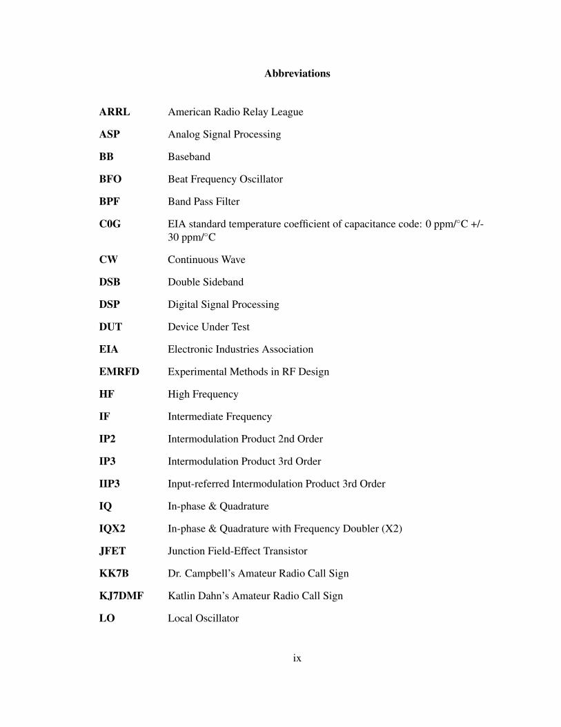
In fact this audio output is not an intermediate frequency, but the final baseband, but this
terminology is a hold-over from superheterodyne terminology. Figure 1.1.3 shows a simple
and typical direct conversion receiver.
Mixer
Local Oscillator
Lowpass Filter
AudioAmplifier
RF Amplifier
Diplexer Filter
Antenna
toheadphones
Figure 1.1.3: direct conversion Receiver with RF amp and IF port filtering.
A benefit of direct conversion is that because the signal only undergoes a single conver-
sion the signal integrity can be much better than the superhet case. The direct conversion
does not have multiple LOs and conversion stages and therefore it has no internally gener-
ated audio pitches, “birdies”. The spurious-free dynamic range (SFDR) of direct conver-
sion receivers can be much higher than the superhet. Additionally it can be seen in Figures
1.1.3 and 1.1.2 that the direct conversion architecture is simpler than the superhet, Figure
1.1.1.
Direct conversion receivers are not, however, immune to limitations. One of which is
that its LO is either exactly the same frequency as the input RF signal, or only an audio
frequency-range distance away. This makes it possible for any leaked or re-radiated LO
energy to become incident on the antenna and be indistinguishable from the desired signal
thereby corrupting it. There are solutions to get around this all of which involving shielding
of the LO signal. LO leakage is particulalry problematic in direct conversion receivers
because it can serve to re-enforce itself. Receiver corruption happens because LO energy
5
at the RF port mixes to produce a DC product, see appendix A and section 1.2, which
imbalances the mixer and allows more LO energy to leak to the RF port. See section 1.2
and reference [4] for more discussion of mixer balance. Another limitation is that direct
conversion receivers are very sensitive to second-order non-linearities, which are distortion
products that can show up right in the receive band near or at DC.
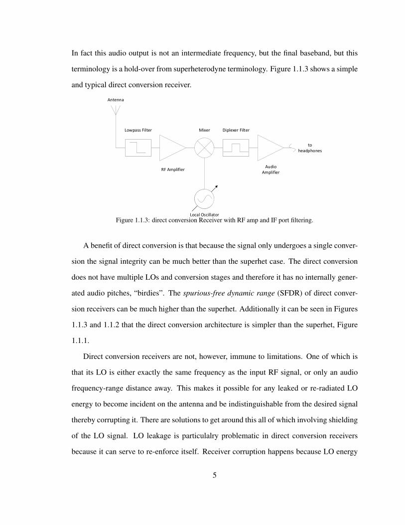
1.2 Frequency Converters
The frequency converter is the block of a receiver and transmitter often referred to as the
mixer. Its basic function for heterodyning is to convert a signal from one frequency to
another either higher, (up-conversion), or lower, (down-conversion), frequency. The way
this is achieved is by multiplying two signals and using the simple trigonometric identity
in Equation A.7.1 to acquire two output terms at the sum, (up-conversion), and difference,
(down-conversion), frequencies of the two input signals.
The presence of the input signals’ frequencies, RF and LO, at the output, IF, depends on
the balance of the mixer. An unbalanced mixer will have both the input signals’ frequencies
present on the output; a single-balanced mixer will cancel one of the input frequencies on
the other ports; and a double-balanced mixer will cancel both input frequencies on the
other ports. The use of circuitry duplication, symmetry, and ideal matching of components
contributes to the cancellation of RF, LO, and/or IF signals at the other ports [4]. Though,
any deviations from these idealities leads to some feedthrough.
IF
50
50
R1
L1C2
C1
LO
RF
C3
50
Figure 1.2.1: Unbalanced JFET mixer [33].
6

Figure 1.2.1 is an example of an unbalanced mixer using a single JFET [33] [4]. RF
and LO signals are applied to the drain and gate, respectively. Low pass filtering at the
drain output passes the IF. But if the RF and LO signals are still able to feedthrough to
the output and other ports, proper filtering on each port is needed to reduce them. The
X-band mixer in [33] by Steven Maas utilizes coupled line and stub filters on the ports to
suppress other port frequencies. This filtering is shown in lumped-element form in Figure
1.2.1 as a diplexer on the drain. In Figure 1.2.2, Figure 1.2.1 has been duplicated and the
LO signal applied differentially to the gates of the two JFETs. The IF output is differential
through a transformer, but because the RF input is single-ended, applied in parallel to the
drains of the FETs. The differential application of LO nulls its frequency at the RF port [4].
Conversely, RF energy at the LO port is cancelled through the transformer null. RF to IF
isolation is improved as the RF is single-ended and the IF taken differentially, but the LO
will be present at the IF output.
50
RF
50C1
LO
R1
L1C2
C1
R1
L1C2 RF
IF
Figure 1.2.2: Singly balanced JFET mixer [7].
An example of a doubly-balanced mixer is the diode ring mixer where both LO and
RF are cancelled at the IF port through symmetry, Figure 1.2.3. Care is needed in termi-
nating the IF mixer port with a wideband 50 Ω load to maintain balance. References [4]
7

and [25] give discussion of proper termination techniques. A diplexer on the IF port is
a popular termination strategy, which KK7B has employed in many designs. There is no
transformer impedance transformation that occurs from the mixer IF port to the RF port [5]
and therefore proper wideband 50 Ω termination at the IF port translates to 50 Ω at the RF.
LO
IF
RF
Balanced
Balanced
Balanced
Balanced
Unbalanced UnbalancedHot-carrier
DiodeRing
Figure 1.2.3: Double-balanced diode ring mixer.
The passive JFET mixer, both singly-balanced and un-balanced, offers very good per-
formance in IIP3 due to high linearity and can have very low noise-figures [33] [34]. The
FET mixer, however, suffers from low 2nd order distortion (IP2) [2], whereas the diode
ring mixer shows good IP2 performance though its noise Figure and IIP3 performance are
often not as good as its JFET counterpart. Because 2nd order linearity is so important for
direct conversion receivers and the conversion loss between the passive FET mixer and the
diode ring are comparable, the diode ring was chosen as the candidate for the iqx2 [2].
Additionally, active mixers like the ubiquitous Gilbert cell mixer are not typically top
choices for high performance direct conversion receivers [30]. This is because the mixer in
a direct conversion application comes before any significant channel selectivity and would
therefore apply amplification to desired and undesired signals alike. Minimal amplification
is therefore presented before the mixer in a direct conversion receiver, with the exception
of a LNA with good reverse isolation, which is important for typical receiver noise Figure
definition as well as improved LO-RF isolation.
8

In low-IF applications, the image channel is separated by two times the IF frequency.
In many practical cases, this is too close to the desired channel to be effectively filtered
out, especially if large signals are present in the image band. In low-IF cases it is possible,
with very sharp filters, to remove the image band from the receiver. However, they are
very difficult to achieve at frequencies above 50 MHz, not to mention there is excess loss
on desired weak signals. An alternative to filtering that can offer good performance is
called a phasing method discussed in great detail in EMRFD chapter 9 [6]. The idea of
phasing is similar to what happens in the balanced cases of the mixers mentioned, signal
cancellation happens through combining signals with opposite phase. A mathematical and
visual frequency domain explanation of phasing in receivers is summarized in appendix A.
With phasing, the limitation of the steepness of filters’ out of band rejection and the
frequency limitations of those filters is eliminated. Theoretically the phasing method is ca-
pable of achieving perfect image-rejection, though practically 30-40 dB of image rejection
is routinely observed [30] due to device mismatches. The IQ mixer is a good choice for di-
rect conversion applications to reduce/reject the image and therefore reduce noise inflicted
on the received signal.
1.3 Organization of Thesis
The progression of this report by chapter number will be as follows: (1) Receiver archi-
tectures and the present direct conversion architecture; Frequency conversion methods and
the present double-balanced diode-ring IQ method; (2) description of the IQ mixer module
first version; (3) Enhancement of the IQ module to the present version, iqx2, explored in
this work; (4) Integration of the half-frequency VFO for fixed LO drive-level; (5) Measure-
ment, discoveries and improvements; iqx2 measurements, the first problem of LO drive-
level sensitivity; VFO initial measurements, the second problem of frequency driftiness and
the source of the problem; (6) Exploration into solutions for VFO frequency drift, applica-
9

tion of solution and resulting measured stability performance; (7) conclusion, summary of
work done and further work towards a complete direct conversion receiver.
10

Chapter 2IQ Crystal Set
The iqx2 module was designed with key direct conversion receiver performance character-
istics in mind. As mentioned direct conversion receivers for low-IF applications have an
image that is very close to the desired band and thus difficult to filter. Superherterodyne
receivers can suffer from this problem too, if the IF is too close to the desired band or if the
band frequency is too high for high selectivity filters. Thus it is common for superhets to
employ multiple conversion with a high first IF. The use of an in-phase, I, and a quadrature,
Q, representation of the input RF signal is useful in that the 90 phase difference between
I and Q channels can be used to destructively interfere with the undesired signal after the
signals are converted and an additional 90 has been applied to I or Q. The math explaining
this can be found very comprehensively in Chapter 9 of EMRFD [6], a summary of which
has been provided in appendix A along with a frequency-domain visual representation.
90° phaseshift
PowerCombiner
90° phaseshift
Local Oscillator input
RFinput
IFSSB
Output
-3dBSplitter
Splitter
Q Mixer
I Mixer
Low-PassFilter
Low-PassFilter
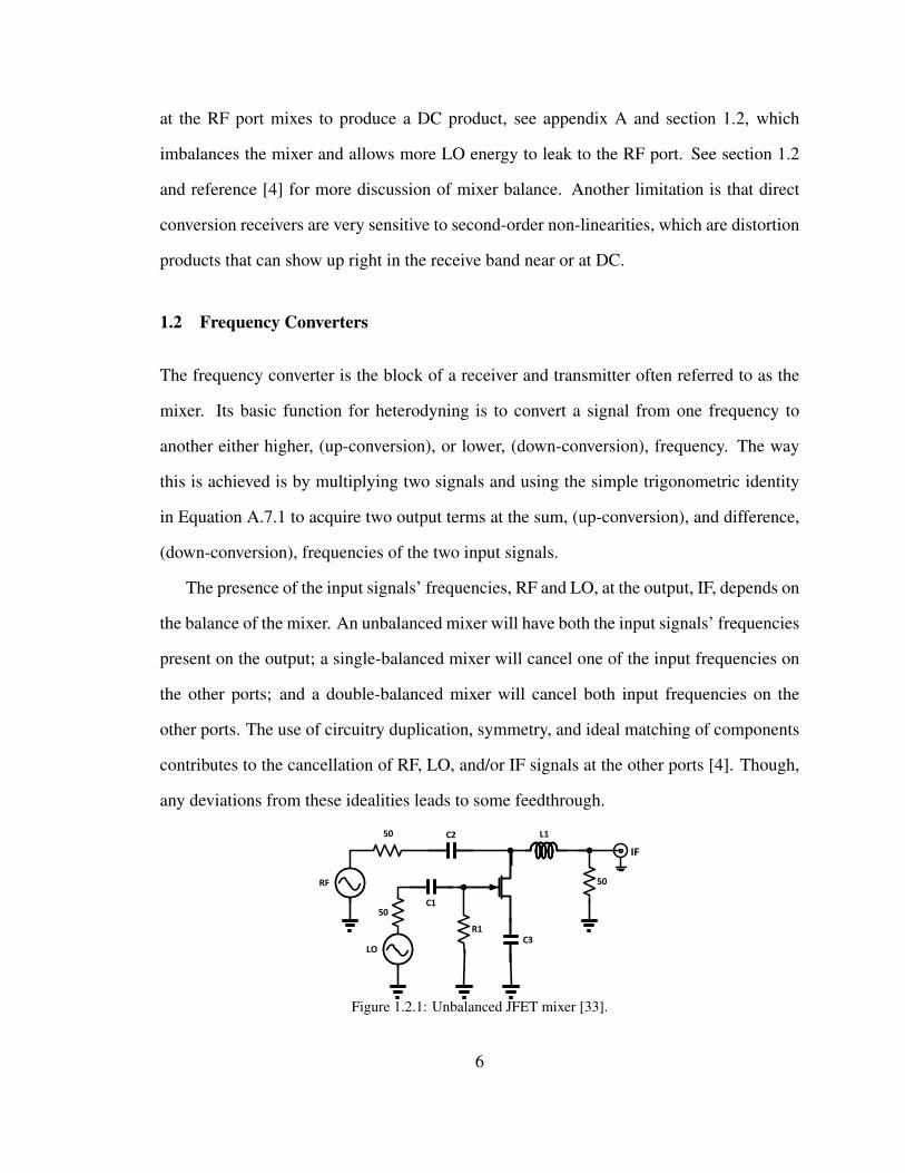
Figure 2.0.1: Hartley IQ Image Reject Mixer for SSB.
Figure 2.0.1 shows a generic block diagram of an IQ image-reject mixer with an I
11
and a Q mixer and with quadrature placed on the LO signal, i.e. 90 phase shift. For
wideband applications it is useful to place quadrature on the LO, but for direct conversion
applications the bandwidth is narrow and placing quadrature on the RF is also suitable.
Narrow-bandedness allows dual purpose of the selectivity components in the signal paths
in providing proper mixer port terminations [2].
I out
Q out
RF in
a b
a
b
LO in
Figure 2.0.2: IQ mixer with single SPDT switch [2]
Figure 2.0.2 shows the scematic diagram of the IQ crystal set described in [2] for the
diode ring mixer case. The interesting thing here is that a single single-pole-double-throw,
SPDT switch as the mixer was used instead of the typical dedicated I and Q mixer seen
in Figure 2.0.1. With quadrature on the RF path, the I and the Q are alternately connected
to the mixer and to ground so the mixer works as if the I and Q had dedicated mixers.
The article [2] also explored a singly-balanced MOSFET switch in place of the diode ring
mixer, but measured second-order non-linearity performance was not as good as the diode
ring nor the measured IQ stability.
12

Chapter 3Enhancements to the IQ Crystal Set: IQX2
The iqx2 explored in this work sports a few enhancements from its previous predeces-
sor: frequency doubling, and a LO-RF DC offset trim. The author’s professor made these
enhancements and a few cursory measurements on their performance before passing the
module on to the author. The idea was for the author to make some measurements on the
iqx2 and discover something for which to base a thesis on. The ensuing measurements and
subsequent unfolding of this thesis’s work is discussed in chapter 5. In this chapter, the
general functioning and purpose of the iqx2 enhancements is discussed.
d
e
I out
Q out
RF in
LO in
e d +
a b
a
b
c
c
Figure 3.0.1: The IQX2 with frequency doubler and LO-RF offset derivation.
The addition of the frequency doubler is good practice especially for use in a direct
conversion receiver to help against the LO leakage problem because it allows use of a LO
frequency at half the operating frequency. Thus if the LO were able to leak out and become
13

incident on the antenna, it would be far enough away to filter out. Additionally, any residual
LO energy that made it to the RF port would not produce a DC output.
The self-mixing of the LO, and the ensuing DC output, does not carry any information
to corrupt the desired signal, but will imbalance the mixer. This imbalancing action cor-
rupts the natural cancellation of balanced signals at the mixer ports because the otherwise
balanced signals have amplitude discrepancies from the DC. This consequently allows even
more LO energy to appear at the RF port of the mixer, which has the ultimate undesired ef-
fect of degrading the opposite sideband suppression, as well as allowing AM demodulation
from degraded 2nd-order non-linearity performance.
The other enhancement to the IQ crystal set was offset trim for the IQ signal paths to
null the LO at the RF port. This can be seen in Figure 3.0.1 at points ‘d’ and ‘e’. The
frequency doubler produces a small amount of DC at the output of the frequency doubler
at point “c”, and this is used to derive trimmable DC offsets at the I and Q branches with
potentiometers at points “d” and “e”. This enhancement is also aimed at improving the
LO-RF isolation and image-rejection (opposite sideabnd suppression). Residual LO at the
RF port can be tuned out by tuning the DC offsets at I and Q. These I and Q DC trims could
also be used to cancel a problematic AM signal frequency and thereby improve 2nd order
distortion [1]. This would be done by applying an off-frequency AM signal at the RF port
and tuning it out, at the output, with the DC offset trims [1].
14

Chapter 4Half Frequency VFO
The trimming IQ DC offset enhancement had an interesting side-effect of making the iqx2
opposite sideband suppression LO drive-level dependent [1]. This was interesting because,
in contrast, the 2015 IQ crystal set with the diode-ring mixer—but without the frequency
doubler—displayed very low variability with LO changes [2]. Measurements of this dis-
covery are presented in chapter 5. This LO drive-level sensitivity was the first problem
discovered in this work and lead to the construction of a fixed-level VFO at half frequency
to stabilize the image-rejection performance. A classic Hartley oscillator was chosen as the
VFO topology.
C4
R1
C3
R1
C3
LM78L06
C1
R2
C2
C5
C6
+12 V
VFOout
Figure 4.0.1: JFET Hartley VFO schematic.
The JFET Hartley VFO of Figure 4.0.1 is a classic design found in many HAM radio
projects, not least those by W7EL, W7ZOI, and KK7B and found in many texts [4] [16]
[22] and papers [27] [28] [29]. The microR2 40m version was taken as the base model
for this work’s LO and was built by the author on the original microR2 prototype board,
Figure 4.0.2, of KK7B to serve as a benchmark. The microR2 [27] LO output was about
+10 dBm at 7 MHz. Next the VFO was scaled to work for half the frequency, at 3.5 MHz.
15

Figure 4.0.2: 3.5 MHz VFO built on a microR2 original prototype board [27].
At first, the author having already hand wound the tapped inductor on FT43-7 toroid for 7
MHz and fastened it into the board, thought to save time and re-use this inductor and scale
the tank capacitor by 4x for the half frequency. This produced a non-oscillating circuit and
further contemplation as to why suggested that there was too much capacitance to sustain
oscillation. The Q of the LC tank can be roughly approximated as an RLC series circuit
with the resistive losses assumed from the inductor, the Q to first order can be expressed
in Equation 4.0.1. The oscillations were likely unable to start due to the lowering of the
Q by about half when the capacitor was scaled up by 4. Therefore a new tapped inductor,
scaled up by 2, was built and paired with capacitance, scaled up by 2, and oscillations had
no problem starting.
Q =1
R
√L
C(4.0.1)
The scaled oscillator, however, had a problem—frequency drift. This was observed
on the spectrum analyzer as the signal swiftly marched off the screen. The author built
the oscillator with available components from the author’s junk box because, plagued by
a myopic condition common to all novices—in a word, ignorance—the “NP0” and “C0G”
footnotes on the schematics did not have much meaning. This was until the observation
16

0.1μ
1M
4.7pNP0*
LM78L06
150
172pNP0*/S.M.**
0.1μ
30 15V
+12 V
VFOout
1.6 -11.2p
air
52t T-50-6#28 magwire
12t tap3t link
+
+ 6v
Fixed caps comprised of multiple caps
incl. temperature
compensating cap
J310
*0 ppm/°C**silver mica
Figure 4.0.3: JFET Hartley VFO schematic with 80m (3.5 MHz) component values.
5.973897457
-22.51563644
-19.14134979
-29.76460266 -29.32982445
-39.34534836 -39.27920914
-54.02486801
-120
-110
-100
-90
-80
-70
-60
-50
-40
-30
-20
-10
0
10
20
1 3 5 7 9 11 13 15 17 19 21 23 25 27 29
po
wer
leve
l (d
Bm
)
Frequency (MHz)
3.5 MHz JFET VFO Spectrum with 3dB attenuator5v Bench Supply drawing 7mA
Figure 4.0.4: JFET Hartley VFO spectrum with +3.86 dBm output power with 3 dB attenuator on output.HD2 -28.5 dBc and HD3 -24 dBc.
of the VFO’s frequency drift, and a subsequent hunt for solutions to better understand and
to solve the problem. Fortunately, oscillator frequency drift is a problem with lots of in-
teresting history and significance in radio design, meaning there is ample literature on the
subject. Radio receivers have a great concern for frequency stability of the local oscilla-
tor, especially for suppressed carrier SSB, because instability may render desired signals
uncapturable, and/or audio receptions unpleasant or unintelligible. Of the few common
17

culprits for frequency instability, ambient temperature variation-induced frequency drift is
considered in this work. The temperature compensated circuit with component values is
shown schematically in Figure 4.0.3, and photographically in Figure 4.0.2. The oscillator’s
output spectrum is shown in Figure 4.0.4. The method of achieving the frequency stability
is discussed in chapter 6. Once the oscillator was built and stabilized, it was then put to use
to solve the opposite sideband suppression LO drive-level sensitivity problem of the iqx2
module, which is discussed in chapter 5.
18

Chapter 5Measurements and Discoveries
The initial measurements of the iqx2 in this work, where we found that the opposite side-
band suppression of the iqx2 module was LO drive-level dependent, are shown in Figure
5.0.2, using the test setup in Figure 5.0.1. As mentioned, this was an unintended side-effect
of deriving the IQ LO-RF, (or off-frequency AM suppression), DC offset trim from the
negative DC produced by the frequency doubler circuitry [1]. The LSB is the sideband
being suppressed with the phasing IQ image reject mixer, iqx2. It is common for single
sideband (SSB) receivers in the HF bands to suppress the lower sideband in favor of the
upper sideband. Both sidebands were measured, first the USB 2 kHz above twice the LO
frequency and then the RF signal generator (SG) was tuned 4 kHz down through zero-beat,
(equal to LO frequency), to 2 kHz on the other side of twice the LO, (twice because of the
frequency doubler). Then for determining the opposite sideband suppression, the differ-
ence between the USB and LSB levels, in dBm, was calculated as the opposite sideband
suppression, or image rejection, in dB.
IF audioLO
RF
RSA3380CSpectrum Analyzer
0Hz – 3kHz span
IQX2 mixerModule
φ and α adjust
HP8648CSignal Generator3.5 MHz
HP8648CSignal Generator6.998-7.002 MHz
Figure 5.0.1: The iqx2 opposite sideband suppression signal generator test setup.
Measurements with signal generators, Figure 5.0.1, iqx2 showed that a drive-level of
19

Figure 5.0.2: The iqx2 opposite sideband suppression sensitivity to LO drive-level with the signal generatortest setup of Figure 5.0.1 at 3.5 MHz LO.
+10 dBm yielded the highest opposite sideband suppression, sweeping RF input levels
from -50 dBm to -90 dBm, Figure 5.0.2, and tuning the amplitude adjust in the iqx2. The
LO frequency was fixed at 3.5 MHz for this test. The opposite sideband suppression was
then tested across the band, (for three LO frequencies), by varying the LO drive-level while
keeping the RF input level fixed at -60 dBm, Figure 5.0.3. It is not as clear from the LO
drive-level sweep over frequency, Figure 5.0.3, that +10 dBm is the best choice. This is
because +10.6 dBm, at the top of the band, produced higher opposite sideband suppression,
but +10 dBm held 45 dB+ opposite sideband suppression across the band, so this was
chosen as the optimal LO drive-level.
The first scaled VFO the author built, scaled from 7 MHz to 3.5 MHz, resulted in lower
output power—about +8 dBm versus +10 dBm. The author tried to think of a convenient
way to increase the output power level without changing the power supply and the board
voltage regulator setup. The author observed that, in the scaling process, the coupling ca-
20

7 8 9 10 11 12 13
LO Drive (dBm)
25
30
35
40
45
50
55
Opp
osite
Sid
eban
d S
uppr
essi
on (
dB)
Opposite Sideband SuppressionSG Test Across Band
3.5 MHz3.5075 MHz3.524 MHz
Figure 5.0.3: The iqx2 opposite sideband suppression sensitivity to LO drive-level and frequency with thesignal generator test setup of Figure 5.0.1 RF input level fixed at -60 dBm.
pacitor on the JFET gate had not been touched. The halving of the oscillator frequency
meant that the impedance of this coupling capacitor was effectively doubled, which conse-
quently increased the voltage drop across it. The author predicted that if the capacitance
was scaled up by about 2, then—being in series with the tank voltage—the voltage drop
across the coupling capacitor would decrease, and the voltage swing across the tank would
therefore increase. The output power increased to roughly +10 dBm when the coupling
capacitor was increased to 5.8 pF from the previous 2.9 pF, supporting the prediction. This
was an experimental result, not rigorously informed from theory, but it produced the de-
sired output power level and was used to replicate the signal generator test results. Later
tests, discussed in this chapter, revealed the errors of this result, and the coupling capacitor
value was accordingly decreased to the 4.7 pF shown in Figure 4.0.3.
The problem was that +10 dBm from the VFO did not yield anywhere near the 45
dB+ opposite sideband suppression results observed from the signal generator test, (Fig-
21

Table 5.1: The iqx2 opposite sideband suppression with VFO utilizing variable coupler to vary LO drive-level.
LO
(MHz)
x2 LO
(MHz)
LO level
(dBm)
RF level
(dBm)
USB
(dBm)
LSB
(dBm)
OSS
(dB)
10.62 -60 -35.4 -59.1 23.7
-50 -26.35 -48.19 21.84
-50 -26.4 -48.8 22.4
3.4739 6.9478 10.29 -50 -26.55 -52.8 26.25
3.4710 6.9420 10.16 -50 -26.59 -53 26.41
-50 -26.5 -46.14 19.64
-60 -36.1 -56.02 19.92
9.9 -50 -26.7 -56.5 29.8
-50 -26.9 -58.1 31.2
-60 -36.42 -67.8 31.38
-70 -46.41 -77.8 31.39
-80 -56.4 -85.9 29.5
3.4649 6.9297 9.87 -50 -26.58 -57.5 30.92
3.4691 6.9381 10
9.85
3.4826 6.965310.6
3.4665 6.9329
ures 5.0.2 and 5.0.3). Opposite sideband suppression levels of about 22 dB were observed
with the VFO for LO level +10 dBm, Table 5.1. Since the +10 dBm LO drive-level did not
match the expected results, the drive-level output was varied to search for the most optimal
LO level with the free-running VFO setup. At first, the output drive-level was varied by re-
placing the JFET gate coupling capacitor with a variable capacitor, informed from previous
experimental results, which increased the output drive-level. This produced poor results,
Table 5.1, where the best suppression was 31 dB at +9.85 dBm drive-level.
C4
R1C3
R1C3
LM78L06
C1
R2
C2
C5
C6
+12 V
VFOout
IF audioLO
RF
JFET HartleyVFO
3.527 MHz
HP8648CSignal Generator
7.052-7.056 MHz RSA3380CSpectrum Analyzer
0Hz – 3kHz span
IQX2 mixerModule
φ and α adjust
Figure 5.0.4: The iqx2 opposite sideband suppression test setup with signal generator for RF input and VFOfor local oscillator (LO).
22

The variable capacitor did indeed produce a variable output drive, but at a cost that
the author had not understood; the output frequency was also varying based on the output
drive-level. But it was varying by an amount that suggested that the JFET’s gate-source
capacitor (Cgs) was participating in the LC tank. An unaccounted for 4 pF or so would be
affecting the output frequency at the highest output power-levels. The J310 JFET datasheet
stated that the nominal Cgs was about 4 pF, which corroborated the observed stray 4 pF of
frequency variation. Through private correspondence with Wes Hayward (W7ZOI) [17],
and further reading from the oscillator section of EMRFD [4], the purpose of the coupling
capacitor was understood. The gate coupling capacitor couples loop power back to the gate,
but it also forms a capacitive divider with the JFET’sCgs. This can be seen in the equivalent
small-signal model of Figure 5.0.5, where C3 is the variable coupling capacitor. The larger
the coupling capacitor—relative to the JFET’sCgs—the larger the oscillator’s output power,
and the more the Cgs capacitor participated in the LC tank oscillation frequency. The
coupling capacitor is therefore recommended to be as small as possible for reliable starting
[22], to ensure isolation between Cgs and the tank.
C4
R1
C3
R1
C3
LM78L06
C1
R2
C2
C5
C6
+12 V
VFOout
G
S
D
Cgs Vgs gmVgs
C3
ro
Figure 5.0.5: Equivalent JFET small-signal model (left) with coupling capacitor on the gate forming voltagedivider with Cgs.
As the +10 dBm LO drive did not serve to replicate the signal generator test results, and
tuning the output power of the VFO with the variable coupling capacitor on the gate did not
serve to produce anything much better, the author turned to other potential culprits. The
23

author thought that this might be due to the VFO possessing poor phase noise, but review
of the literature of this Hartley oscillator [22] suggested this was the wrong conclusion.
The expected phase noise from previously measured versions of this circuit were about
-146 dBc/Hz at 20 kHz offset [4] [22]. The author attempted to measure the phase noise
in the lab with available equipment, but encountered instrument limitations. The signal
generators used for the tests (HP8648C) had phase noise, stated in the datasheet, to be <-
120 dBc/Hz at a 500 MHz carrier [41]. The datasheet did not have data for 3.5 MHz center
frequency, but it may be expected to be a little better than -120 dBc/Hz.
Figure 5.0.6: Phase noise of VFO measured with R&S FSWP.
The signal generator phase noise could not be measured at the 20 kHz offset, however,
with the spectrum analyzer the author had at hand (RSA3308C), because its own phase
noise—at a 20 kHz offset from a 1 GHz carrier—was -108 dBc/Hz [42]. Thus the spectrum
analyzer’s own internal phase noise was likely to be worse than the DUT’s as well as the
signal generator’s, meaning too much phase noise to reliably measure the DUT’s own phase
24
noise. The author was able to use a Rohde & Schwarz phase noise spectrum analyzer
(FSWP) at work, and measured -149 dBc/Hz at a 20 kHz offset, Figure 5.0.6. The phase
noise measurements were made with the VFO unshielded and open in the lab.
After the phase noise measurements, the author was convinced that the phase noise of
the oscillator was not leading to the poor opposite sideband suppression. Instead, the author
investigated other fundamental differences between the two setups: signal generator for
LO, vs. free-running Hartley VFO for LO. One significant difference was that the signal
generator provided a wideband 50 Ω load to the frequency doubler input, and the VFO
output was not 50 Ω as it was a 3-turn link directly off the JFET Hartley tank inductor.
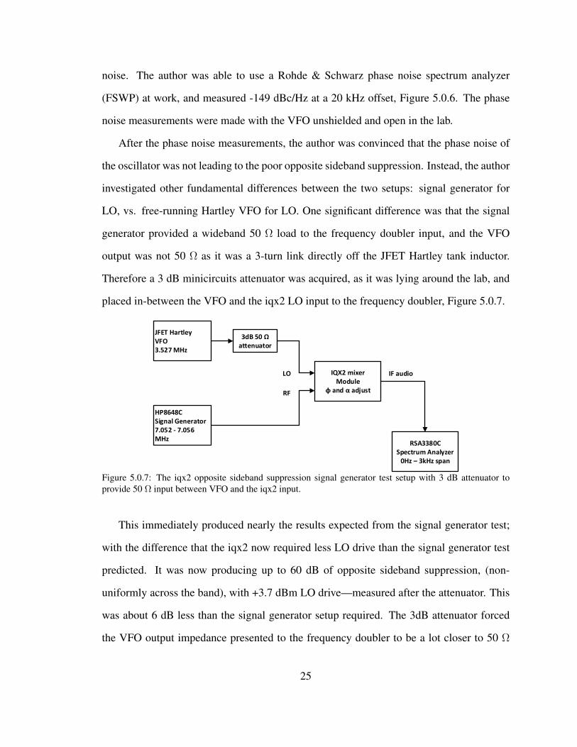
Therefore a 3 dB minicircuits attenuator was acquired, as it was lying around the lab, and
placed in-between the VFO and the iqx2 LO input to the frequency doubler, Figure 5.0.7.
IF audioLO
RF
3dB 50 Ωattenuator
JFET HartleyVFO3.527 MHz
HP8648CSignal Generator7.052 - 7.056 MHz
RSA3380CSpectrum Analyzer
0Hz – 3kHz span
IQX2 mixerModule
φ and α adjust
Figure 5.0.7: The iqx2 opposite sideband suppression signal generator test setup with 3 dB attenuator toprovide 50 Ω input between VFO and the iqx2 input.
This immediately produced nearly the results expected from the signal generator test;
with the difference that the iqx2 now required less LO drive than the signal generator test
predicted. It was now producing up to 60 dB of opposite sideband suppression, (non-
uniformly across the band), with +3.7 dBm LO drive—measured after the attenuator. This
was about 6 dB less than the signal generator setup required. The 3dB attenuator forced
the VFO output impedance presented to the frequency doubler to be a lot closer to 50 Ω
25

and brought the two test setups closer to a valid comparison. This test setup, with the 3 dB
attenuator, can be seen in Figure 5.0.7. The final opposite sideband suppression with the 3
dB attenuator can be seen in Table 5.2. Above 40 dB opposite sideband suppression was
achieved for small variation in power supply (4.2 - 4.5 V) and LO drive-levels +2.25 dBm
- +5 dBm.
Table 5.2: The iqx2 opposite sideband suppression with temperature compensated VFO utilizing the testsetup of Figure 5.0.7. 4.7pF non-NP0 ceramic capacitor used for coupler on JFET gate.
current iqx2 voltage LO level LO Freq RF level USB LSB OSS x2 LO Freq SB
mA V dBm MHz dBm dBm dBm dB MHz (USB)
-50 -27.35 -49.8 22.45
-60 -37.04 -59.8 22.76
8 6.98 10.01 3.4883 -60 -37.08 -59.98 22.9 6.9787
-60 -38.57 -70.5 31.93
-50 -28.96 -60.66 31.7
-70 -48.9 -80.56 31.66
-60 -38.88 -80.3 41.42
-50 -30.3 -70.7 40.4
-60 -40.34 -85.6 45.26
-50 -30.52 -77.2 46.68
-60 -40.41 -82.8 42.39
-50 -30.58 -73.5 42.92
-50 -31.01 -91 59.99
-40 -22.48 -79.2 56.72
-50 -31.3 -84.5 53.2
-60 -41.16 -92 50.84
-70 -51.16 -93 41.84
-50 -31.55 -81.2 49.65
-60 -41.42 -90 48.58
-60 -43.3 -79.7 36.4
-50 -33.4 -69.7 36.3
6
6
6
5
7
4.5
4
4.4
4.25
10.05
6.6
5.04
0.56
4.54
2.76
2.25
4.47
4.2
4.39
8
6
6
6
6.98163.4898
3.4883 6.9787
3.490416.9828
3.490986.9840
3.4905456.9831
3.490735
6.9835
6.98363.490795
3.490556.9831
6 4.3 3.743.490675
6.9834
6
26

Chapter 6VFO Frequency Drift
Once the driftiness of the VFO was observed and communicated to the author’s professor,
he suggested that the source of the driftiness— considering the component choices—was
from the tank components. He subsequently supplied the author with higher quality parts.
Immediately upon replacing the poly trimmer capacitor and ordinary ceramic capacitors
with an air-core sliding-plate variable capacitor and silver mica capacitors, the oscillator
output could be seen on the spectrum analyzer without whizzing off the screen. This was
enough to prove that the temperature variability was arising from the temperature variability
of the tank components, so at a minimum the tank capacitors were implicated.
A search for frequency stabilizing methods, including a method by Wes Hayward [14],
was conducted in this work with the advice of the author’s professor. Wes Hayward’s
method was attractive in the sense that the needed test equipment was at hand. Construc-
tion of additional equipment was easily achieved and explained in the article. The list of
required equipment for the temperature compensation tests and the equipment used is as
follows:
1. Frequency Counter : CMC2512. Thermometer : partial-immersion (red spirit)3. Temperature Chamber : styrofoam cooler4. Heat source : light bulb5. Separator : piece of bamboo board6. Fan : 12v computer GPU fan (optional)
The author built the recommended temperature chamber from reference [14]. The
chamber can be seen in Figure 6.0.1. The left picture is a closed-view of the chamber,
with the styrofoam box (3), the thermometer sticking out (2), the VFO power supply and
output cables below to the left, and the fan (6) with a removable cover below on the ground.
27

Figure 6.0.1: Temperature Chamber for temperature compensation tests [14]
The thermometer could alternatively be a digital one, but calibration would be needed [14].
The fan was installed into the side of the chamber to fascilitate removing heat from inside
the chamber. An additional fan could be used internally to help improve thermal conduc-
tion, but care would have to be expended so that mechanical stress is not imparted to the
DUT, [14].
The right picture of figure 6.0.1 is an open-view showing the light-bulb heat-source
(4), separator (5) for the DUT, and a small platform for the DUT in the bottom left corner.
The separator is a miniature internal wall that is needed to keep the light-bulb radiation
from directly impacting the DUT. The platform was used to elevate the DUT because heat
tends to rise, and the thermometer was placed at the same level as the DUT. A piece of
bamboo board was used both for the separator and for the base of the temperature chamber.
Styrofoam works very well as it is a good insulator. Only 3 sides and the top of the chamber
were styrofoam, but the thermal insulation was still sufficient.
The basic idea of the temperature compensation technique was to measure the temper-
ature variability of the oscillator and, with some basic assumptions, calculate the tempera-
ture coefficients (TC) of the tank components and replace some tank components with parts
possessing equal and opposite temperature coefficients.
28
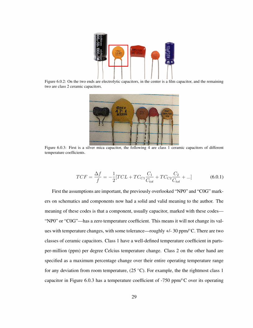
Figure 6.0.2: On the two ends are electrolytic capacitors, in the center is a film capacitor, and the remainingtwo are class 2 ceramic capacitors.
Figure 6.0.3: First is a silver mica capacitor, the following 4 are class 1 ceramic capacitors of differenttemperature coefficients.
TCF =∆f
f= −1
2[TCL+ TCC1
C1
Ctot
+ TCC2C2
Ctot
+ ...] (6.0.1)
First the assumptions are important, the previously overlooked “NP0” and “C0G” mark-
ers on schematics and components now had a solid and valid meaning to the author. The
meaning of these codes is that a component, usually capacitor, marked with these codes—
“NP0” or “C0G”—has a zero temperature coefficient. This means it will not change its val-
ues with temperature changes, with some tolerance—roughly +/- 30 ppm/C. There are two
classes of ceramic capacitors. Class 1 have a well-defined temperature coefficient in parts-
per-million (ppm) per degree Celcius temperature change. Class 2 on the other hand are
specified as a maximum percentage change over their entire operating temperature range
for any deviation from room temperature, (25 C). For example, the the rightmost class 1
capacitor in Figure 6.0.3 has a temperature coefficient of -750 ppm/C over its operating
29

Figure 6.0.4: VFO drift with initial parts available from junk box.
Figure 6.0.5: VFO warmup drift with initial parts available from junk box, 12.2 kHz in 45 min and climbing!
30

temperature range, with 5 % value tolerance. In contrast, the boxed capacitor in Figure
6.0.2 is a class 2 ceramic capacitor with maximum percent capacitance change +/- 22 %
over its temperature range, (-30 C to +85 C), with 20 % value tolerance. This corresponds
to about 220,000 ppm maximum variation for an unspecified degree deviation from room
temperature. Class 2 ceramic capacitors are less stable with temperature variations than
class 1, but they are able to have much higher capacitance values for their size [47].
The idea is to replace all tank capacitors with stable 0 ppm/C parts and to measure the
temperature coefficient of frequency (TCF) in a controlled temperature environment. The
time, temperature, and the frequency are measured and recorded. The tank capacitors could
be NP0/C0G parts or silver mica capacitors, which also typically have low temperature
coefficients. The tank inductor, being wound with magnetic wire on powdered iron toroid
core, typically has some appreciable amount of positive temperature coefficient.
Figure 6.0.6: VFO drift after changing a few key components in the tank circuit.
31

By replacing all the capacitors with zero temperature coefficient parts, the measured
temperature drift can be assumed to be produced solely by the inductor. Equation 6.0.1 [4]
[14] gives the relationship between TCF and the inductor temperature coefficient (TCL) and
temperature coefficients of the tank capacitors (TCCi). With the temperature coefficients of
the capacitors all assumed to be zero, Equation 6.0.1 reduces to the measured TCF equaling
half of the temperature coefficient of the inductor (TCL).
Figure 6.0.7: VFO temperature drift after 1st annealing of inductor -63.8 ppm/C.
Before proceeding with the measurement of the TCF, the unstable junk box capacitors
were swapped back in for the silver mica (SM) capacitors and air core variable capacitor.
Figure 6.0.4 shows the original drift was about +15235 ppm/C, or about +11.5 kHz/C, so
it is no wonder that this was visible on the spectrum analyzer. The warmup characteristic
of the drifty circuit does not settle out even after 45 minutes, Figure 6.0.5; drifting about
12.2 kHz and climbing.
The author next removed the original drifty components, replaced them with Dr. Camp-
bell’s stable silver mica and air core variable capacitor, and the temperature drift measured.
32

Table 6.1: The tank components for calculation of the TCL of the inductor, and for measurements of Figures6.0.7, 6.0.8, and 6.0.10
QTY Cap fixed Cvar Inductor1 100p SM 1.6p-11.2p 11.3µ1 56p SM1 10p NP0
Figure 6.0.6 shows the result. A significant improvement in TCF can be seen in Figure
6.0.4, going from +15235 ppm/C to -55 ppm/C. The temperature stable capacitor val-
ues could only achieve 3.65 MHz, but the results were instructive regardless—exposing
the drifty quality of the original capacitors. More silver mica and NP0 components were
acquired and the VFO tuned down to 3.5 MHz.
Figure 6.0.8: VFO temperature drift after 2nd annealing of inductor -46.94 ppm/C.
A recommendation found in Roy Lewallen’s paper [28] suggested that annealing the in-
ductor, to temperature condition it, makes it less variable with temperature. The tapped in-
ductor of the Hartley oscillator was wound on a powdered-iron toroid core with magnetically-
33

Figure 6.0.9: Boiling of entire circuit in pot of water on the stove to anneal inductor.
insulated wire and annealing likely temperature-conditions the wire windings to have a sta-
ble temperature coefficient. The resultant temperature drift of the 3.5 MHz circuit after an-
nealing one and two times can be seen in Figures 6.0.7 and 6.0.8, respectively. Figure 6.0.7
has -63.8 ppm/C TCF, and the 2nd annealing of Figure 6.0.8 shows marginal improvement
to -46.94 ppm/C TCF. The warmup characteristics, however, became noticeably more sta-
ble with each annealing, Figure 6.0.10. The warmup drift before annealing is greater than
650 Hz in more than 70 minutes, with 500 Hz of the drift occurring in the first 20 minutes.
After the first annealing the warmup improves to about 320 Hz, most of which occurs in
the first 17 minutes, but still continues to drift after 120 minutes. After the 2nd annealing,
the warmup drift was about 100 Hz, stabilizing well after about 17 minutes. The inductor
had already been placed on the board, so the entire circuit was boiled in water for about
5 minutes for the first annealing, and 10 minutes for the second annealing. Figure 6.0.9
34

shows the oscillator board in a pot of boiling water on the stove.
Figure 6.0.10: Comparison of warmup of oscillator before and after annealing one and two times.
TCL =(−2) TCF − TCC1C1
Ctot
− TCC2C2
Ctot
|TCci==0
=(−2)(−63.8)
= + 128ppmC
(6.0.2)
TCL =(−2) TCF − TCC1C1
Ctot
− TCC2C2
Ctot
=(−2)(−63.8)− (−50)100pF
177.2pF− (−50)
56pF
177.2pF
= + 171ppmC
(6.0.3)
After the first annealing, the temperature coefficient of inductance (TCL) was calculated
by rearranging Equation 6.0.1, to solve for the TCL, Equations 6.0.2 and 6.0.3. Equation
6.0.2 assumes ideal zero temperature coefficient capacitors, and thus the TCL is just 2x the
measured TCF. Equation 6.0.3 introduces some component non-idealities, discussed in the
35

following paragraphs.
TCF |=0 = −1
2[ TCL+ TCC1
C1
Ctot
]
TCC1 = −128 (177.2p
56p)
= −405ppmC
(6.0.4)
The author chose a 56 pF capacitor as the compensating capacitor, and the temperature
coefficient (TCC1) was calculated using the ideal TCL of +128 ppm/C and a TCF of zero,
Equation 6.0.4. The TC was calculated to be -405 ppm/C, but the closest standard TCs
were -330 (N330) or -470 (N470). Neither N330, nor N470 for 56 pF could be located
online or elsewhere. Instead, a heuristic measurement with an acquired 56 pF N750 capac-
itor was performed to test how well the mathematical model fit measurements. Equation
6.0.5 shows the prediction of -54.5 ppm/C TCF, assuming the ideal calculated TCL (+128
ppm/C) and -750 ppm/C for the TC of the 56 pF capacitor. A temperature sweep was
performed in the temperature chamber to measure the TCF, using the tank components in
Table 6.2. Figure 6.0.11 shows the measured TCF of +85 ppm/C.
Table 6.2: Tank components for fitting the mathematical model. NP0 - 0 ppm/C and SM for silver mica,Figure 6.0.11
QTY Cap fixed Cap Comp Cvar Inductor1 100p SM 56p N750 1.6p-11.2p 11.3µ5 10p NP0
TCF = −1
2[ 128 + (−750)
56p
177.2p]
= −54.5ppmC
(6.0.5)
36

TCF = −1
2[ 150 + (−850)N750
56p
177.2p+ (−15)NP0
10p
177.2p+ (−90)SM
100p
177.2p]
= +85ppmC
(6.0.6)
0 10 20 30 40 50 60 70
Time (min)Temperature Chamber CMC251 freq counter
3523
3523.78
3524.56
3525.33
3526.11
3526.89
3527.67
3528.44
3529.22
3530
Osc
Fre
q (K
Hz)
3.5 MHz compensated JFET oscSM 100pF || N750 56pF || NP0 10pF TCF +85 ppm/degC
22
24.2
26.3
28.5
30.7
32.8
35
37.2
39.3
41.5
Tem
pera
ture
(C
)
X 19Y 23.1
X 31Y 40.1
X 19Y 3524
X 31Y 3529
Figure 6.0.11: Overcompensation with 56 pF N750 compensating capacitor.
The measured +85 ppm/C was used to introduce some component non-idealities into
the mathematical model of Equation 6.0.5, in order to match theory to measurements. Sil-
ver mica (SM) capacitors typically have some nonzero temperature coefficient, (roughly
−50 ppm/C), therefore the TCL was calculated accounting for approximate non-idealities,
Equation 6.0.3. The range of TCL values was calculated to be about−128 ppm/C to−171
ppm/C. The mean of these two values (+150 ppm/C) was used for subsequent TC calcu-
lations and TCF predictions. N750 capacitors have a TC tolerance of +/ − 120 ppm/C,
which provides a temperature coefficient range of −630 ppm/C to −870 ppm/C. To fit
the measured +85 ppm/C TCF to the model, the mean TCL of +150 ppm/C was used,
37

and the N750 was adjusted to −850 ppm/C—close to its maximum. Adjusting the NP0
to −15 ppm/C for the 10 pF capacitor, and the SM 100 pF to −90 ppm/C in Equation
6.0.6, calculated to fit the measured result quite well. Therefore, −90 ppm/C and −15
ppm/C were used for subsequent TC calculations and TCF predictions for SM and NP0
parts, respectively.
TCF = −1
2[ TCL+ TCC1
C1
Ctot
+ TCC2
C2
Ctot
+ TCC3
C3
Ctot
]
= −1
2[ 150 + (−470)
36.8p
180.5p+ (−15)
30p
180.5p+ (−90)
101p
180.5p]
= +0.6ppmC
(6.0.7)
TCF high = −1
2[ 150 + (-410)
36.8p
180.5p+ (−15)
30p
180.5p+ (−90)
101p
180.5p]
= +6.7ppmC
TCF low = −1
2[ 150 + (-530)
36.8p
180.5p+ (−15)
30p
180.5p+ (−90)
101p
180.5p]
= −5.5ppmC
(6.0.8)
Table 6.3: 7.05 - 7.22 MHz tank components, NP0 - 0 ppm/C and SM for silver mica. Figures 6.0.13 and6.0.12, and Equation 6.0.7
QTY Cap fixed Cap Comp Cvar Inductor1 101p SM 36.8p N470 1.6p-11.2p 11.3µ3 10.5p NP0
Temperature stability was achieved at −1.42 ppm/C for frequency range 7.05 - 7.22
MHz with styrofoam packaging placed on the inductor and the capacitors for thermal insu-
lation. Without insulation, −4.25 ppm/C was measured. The temperature compensating
part was a single 36 pF capacitor with temperature coefficient of N470, meaning −470
38

Figure 6.0.12: VFO drift with temperature compensating capacitor and low, (zero) temp-co capacitors forfrequency doubled tuning range 7.05 - 7.22 MHz, (doubled frequency).
Figure 6.0.13: Temperature drift of 7.05 - 7.22 MHz, (doubled frequency), tuned oscillator with styrofoampackaging on tank inductor and capacitors, -1.42 ppm/C.
39

Figure 6.0.14: VFO drift with temperature compensating capacitor and low, (zero) temp-co capacitors forfrequency doubled tuning range 6.95 - 7.13 MHz, (doubled frequency).
ppm/C, Table 6.3. The predicted TCF with this compensating capacitor was +0.6 ppm/C,
Equation 6.0.7, where nominal −470 ppm/C TC was assumed. Non-idealities of the three
10.5 pF NP0 parts were assumed to have -15 ppm/C temperature coefficient. The 101 pF
assumed to have -90 ppm/C temperature coefficient. These non-idealities were informed
from the previous heuristic measurement. This was quite close to the measured −4.25
ppm/C TCF and within the range of tolerance of the N470 TC—−470 +/- 60 ppm/C—
Equation 6.0.8. Temperature stability was also tested for the frequency range 6.95 – 7.13
MHz, which yielded +8.5 ppm/C, Figure 6.0.14. The components used for this test are
listed in Table 6.4.
Table 6.4: 6.95 - 7.13 MHz tank components, NP0 - 0 ppm/C and SM for silver mica. Figure 6.0.14
QTY Cap fixed Cap Comp Cvar Inductor1 85.3p SM 36.8p N470 1.6p-11.2p 11.3µ5 10.5p NP0
40

It is quite a practical challenge to procure stable and specific temperature coefficient
capacitors these days. None could be found in leaded form from Digikey or Mouser. All
of the temperature coefficient and stable capacitors were purchased and scavenged from
SurplusGizmos or received from the author’s professor. The ARRL chapter on Oscillators
[16] notes that the supply of such capacitors is disappearing due to frequency synthesizers
becoming the standard.
41

Chapter 7Conclusion and Future Work
A frequency stabilization technique of Wes Hayward’s [14] to stabilize frequency drift with
temperature of a JFET Hartley VFO has been demonstrated. The requisite temperature
chamber to perform the temperature drift measurements was constructed by the author in
accordance with suggestions of Wes Hayward’s article [14], discussed in chapter 6 of this
work. This work represents the first known presentation of careful measurements of the
improvement in initial and long term frequency drift resulting from immersion of the entire
VFO circuit in boiling water. The VFO frequency drift with temperature was compensated
to -4.25 ppm/C and +8.5 ppm/C for the 40m frequency ranges: 7.05 – 7.22 MHz, and
6.95 – 7.13 MHz, respectively. The frequency drift was further reduced with styrofoam
packaging on the tank components, achieving −1.42 ppm/C. The theoretical frequency
drift model was also heuristically modified to fit measured results to enable more accurate
temperature drift of frequency (TCF) predictions. The resultant adjusted model, Equation
6.0.7, predicted +0.6 ppm/C for the 7.05 – 7.22 MHz compensated VFO, (using the nom-
inal TC of the compensating capacitor), which measured at −4.25 ppm/C. The measured
TCF was within the tolerance of the compensating component’s temperature coefficient,
which predicted a TCF in the range of −6.7 to +5.5 ppm/C, Equation 6.0.8.
Also shown in this work was the solution of the iqx2 [1] with opposite sideband sup-
pression sensitivity to LO drive-level. A fixed-level VFO achieved 40 dB+ opposite side-
band suppression of the iqx2 for LO drive-levels in the range of +2.25 - +5 dBm. Mea-
surement of the phase noise of the JFET Hartley VFO in this thesis using an available
instrument during the author’s internship at Rohde & Schwarz confirmed that this topology
is capable of remarkable performance, significantly better than the signal generators and
measurement instruments in the Portland State laboratories. The phase noise of the VFO
42

was measured and found to be -150 dBc/Hz, which was in accordance with the literature
on this VFO topology [4] [22].
When the VFO was frequency stabilized and applied back to measuring the opposite
sideband suppression of the iqx2 mixer module, more design improvements were made to
the VFO in order to improve opposite sideband suppression. It was discovered that some
50 Ω attenuation was needed between the output of the VFO and the input of the iqx2
to present a wideband 50 Ω load, which improved the opposite sideband suppression to
the 40 dB+ results. Additionally, it was discovered through experimentation and review
of literature [4] that the oscillator’s output power should be varied by varying the power
supply, not through varying the JFET gate coupling capacitor.
This work presents the measurements performed on the experimental iqx2 circuit, the
work done on temperature compensation of the VFO, and the fitting of the VFO into a
working test setup for the iqx2. The method for frequency drift compensation was a prin-
cipally simple one, but which has been expressed as tedious in literature [16]. The author
would not attempt to discount such a claim, but notes that the tedium of the process was
very useful especially for a new HAM radio operator. The experience, to use Dr. Camp-
bell’s phrase, “digging into the onion” and working all aspects of the experiment right down
to building part of the test setup was extremely rewarding and revealing.
Considering the work that has been done here, a complete receiver has still not been
acheived. Further blocks to complete this full direct conversion phasing receiver include
an RF LNA and a low-pass input filter. Additionally, the IQ mixer module and baseband
audio signal processor would be a project for the author to build; the one measured here
is not the author’s property. To use the half-frequency VFO described in this work, some
improvements could be made to the interface of the iqx2. A 3 dB or 6 dB 50 Ω pad at the
output of the VFO would provide a nice wideband 50 Ω termination to the LO frequency
doubler port. Additionally, a low-pass filter would be useful to knock down oscillator
43

harmonics, (which the 3rd harmonic is 24 dB down), Figure 4.0.4. According to EMRFD
[4] even order harmonics can severely imbalance the balanced frequency doubler, Figure
3.0.1, and degrade the suppression of the fundamental feed-through. This might further
compromise the balanced mixer if the fundamental and strong harmonics are both present
at the LO input. It might be worth experimenting further with some filtering of the half
frequency VFO output before the frequency doubler input. Although the second harmonic
is about 28 dB down from the fundamental already, a 3-pole low-pass Chebyshev filter
with cutoff frequency 5 MHz would knock the 2nd harmonic down to about 38 dB down
from the fundamental. Whether the lower harmonic levels from use of the low pass has
an improvement on balance in the frequency doubler and/or mixer could be approximated
by observation of the effect on the opposite sideband suppression. An increase in opposite
sideband suppression with use of the low pass filter with respect to without the low pass
filter might lead to the conclusion that reducing harmonic energy at the frequency doubler
input preserves balance of the frequency doubler and perhaps the mixer. All measurements
with and of the VFO were done with the circuit open on the bench, so the natural next step
would be to build the VFO in a shielded container, an Altoids can would be an ideal choice
as it is the right size and readily available. Some foam packing could be easily installed
for some temperature insulation which would further stabilize any temperature induced
frequency drift.
44

References
[1] Rick Campbell and Katlin Dahn, ”Simple New Analog-RF Weak Signal Receivers”in Proceedings of the 2019 VHF Super Conference, Sterling, VA, April 2019, Amer-ican Radio Relay League, ISBN:978-1-62595-102-1, pp. 196-203
[2] Richard Campbell, Portland State University, ”HF-VHF-UHF IQ Mixer with a SingleSPDT Switch” IEEE MTT-S IMS Conference Paper, May 2015.
[3] Richard Campbell, TriQuint Semiconductor ”An Integrated I-Q Mixer for Software-Defined Radio Applications” High Frequency Design, Jan. 2004, pp 26-33.
[4] Wes Hayward, Rick Campbell, Bob Larkin, Experimental Methods in RF DesignNewington, CT: American Radio Relay League, Inc, 2016 Classic Reprint. Chap. 5.
[5] Wes Hayward, Rick Campbell, Bob Larkin, Experimental Methods in RF DesignNewington, CT: American Radio Relay League, Inc, 2016 Classic Reprint. Chap. 5pp 5.8.
[6] Wes Hayward, Rick Campbell, Bob Larkin, Experimental Methods in RF DesignNewington, CT: American Radio Relay League, Inc, 2016 Classic Reprint. Chap. 9.
[7] Richard Campbell, Notes: ”New Mixer Design Notes” April 26, 2007. [Online].Available: http://web.cecs.pdx.edu/∼campbell/mixnotes.pdf (Accessed on August 09,2019)
[8] Behzad Razavi, RF Microelectronics 2nd Ed. London, UK: Pearson Education, Inc,2012. Chap. 4.
[9] Rick Lyons, ”Quadrature Signals: Complex but not Complicated” White Paper IEEELong Island Section. [Online]. Available: https://www.ieee.li/pdf/essay/quadraturesignals.pdf (Accessed on Jul. 28, 2019)
[10] Rick Lyons, ”Understanding the ’Phasing Method’ of Single Sideband De-modulation” DSPrelated.com. Aug. 8, 2012 [Online]. Available: https : / /www.dsprelated.com/showarticle/176.php (Accessed on August 30, 2019)
[11] Ralph Oppelt, ”The Generation and Demodulation of SSB Signals Using the PhasingMethod Part 1: Basic Theory” VHF Communications, vol. 19, ed 2, Summer 1987,pp 66-72.
[12] Ralph Oppelt, ”The Generation and Demodulation of SSB Signals Using the Phas-ing Method Part 2: Signal Processing for SSB/DSB/AM Transceiver Without UsingCrystal Filters” VHF Communications, vol. 19, ed 3, Fall 1987, pp 130-140.
45

[13] Mike Arnold, Randy Class, Francesco Dantoni, Shrinivasan Jaganathan, and RolandSperlich, Texas Instruments. Application Report SLWA05 ”LO Harmonic Effectson I/Q Balance and Sideband Suppression in Complex I/Q Modulators” May 09,2010. [Online]. Available: http://www.ti.com/lit/an/slwa059/slwa059.pdf (Accessedon Oct. 03, 2019)
[14] Wes Hayward, ”Measuring and Compensating Oscillator Frequency Drift” QST,Dec. 1993, pp 37-41.
[15] Jacob Makhinson, ”A Drift-Free VFO” QST, Dec. 1996, pp 32-36.
[16] David Stockton, Frederick J. Telewski, ”Oscillators and Synthesizers” Newington,CT: ARRL Handbook 2012. Chap. 10.
[17] Wes Hayward, Private Correspondence Jul. 2019.
[18] Wes Hayward, Rick Campbell, Bob Larkin, Experimental Methods in RF DesignNewington, CT: American Radio Relay League, Inc, 2016 Classic Reprint. Chap. 4.
[19] Richard Campbell, TriQuint Semiconductor, ”LO Phase-Noise Management in Ama-teur Radio Receiver Systems” White Paper.
[20] Richard Campbell, ”A Black Box HF-VHF Instrumentation Receiver” White Pa-per. [Online]. Available: http://web.cecs.pdx.edu/∼campbell/iR2ch8.pdf (Accessedon August 09, 2019)
[21] Richard Campbell, ”Direct-Conversion Receiver Noise Figure” QST TechnicalCorrespondence, Feb. 1996, pp 82-84.
[22] Wes Hayward, Doug DeMaw Solid State Design for the Radio Amateur Newington,CT: American Radio Relay League, Inc, 1986. Chap. 3.
[23] Kay Green, Agilent Technologies, Inc, Presentation ”Phase Noise MeasurementsMethods and Techniques” 2012. [Online]. Available: https://www.keysight.com/upload/cmc upload/All/PhaseNoise webcast 19Jul12.pdf
[24] Rhode & Schwarz, Application Note: ”Phase Noise Measurements with Spec-trum Analyzersof the FSE family” Dec. 08, 1995. [Online]. Available: https:/ /scdn.rohde- schwarz.com/ur/pws/dl downloads/dl application/application notes/1epan16/1epan16e.pdf
[25] Richard Campbell, ”High-Performance Direct-Conversion Receivers” QST, Aug.1992, pp 19-28.
[26] Richard Campbell, ”High-Performance, Single-Signal Direct-Conversion Receivers”QST, Jan. 1993, pp 32-40.
46

[27] Richard Campbell, ”The MicroR2 - An Easy to Build “Single Signal” SSB or CWReceiver”, 4th ed., QST, Oct. 2006 pp 28-32.
[28] Roy Lewallen, ”An Optimized QRP Transceiver” QST, Aug. 1980, pp 14-19.
[29] Wes Hayward, Dick Bingham, ”Direct Conversion: A Neglected Technique” QST,Nov. 1968, pp 15-17.
[30] Wes Hayward, Rick Campbell, Bob Larkin, Experimental Methods in RF DesignNewington, CT: American Radio Relay League, Inc, 2016 Classic Reprint. Chap. 8.
[31] Joel Hallas, ”Receivers” Newington, CT: ARRL Handbook 2012. Chap. 12.
[32] Richard Campbell, Notes: ”Medium Power Diode Frequency Doublers”. May20, 1999. [Online]. Available: http://web.cecs.pdx.edu/∼campbell/mixnotes.pdf (Ac-cessed on Jul. 09, 2019)
[33] Stephen A. Maas, ”A GaAs MESFET Mixer with Very Low Intermodulation” IEEETransactions on Microwave Theory and Techniques, vol. MTT-35, no. 4, Apr. 1987,pp 425-429.
[34] Richard Campbell, Cascade Microtech, ”High Frequency Differential Passive FETDirect Conversion Mixer/Modulator” IEEE MTT-S IMS Digest 2006, pp 922-925.
[35] Richard Campbell, ”Microwave Downconverter and Upconverter Update” WhitePaper.
[36] Wes Hayward, personal website. ”Two Faces of Q” Nov. 2010. [Online]. Available:http://w7zoi.net/twofaces.pdf (Accessed on Jul. 06, 2019).
[37] R. Fischer, ”Broadband Twisted-Wire Quadrature Hybrids” IEEE Transactions onMicrowave Theory and Techniques, vol. 21, no. 5, May 1973, pp 355-357.
[38] D. Pozar, Microwave Engineering, 4th ed. Hoboken, NJ: John Wiley and Sons, Inc,2012.
[39] Kenneth K. Kaiser, Kettering University, Electromagnetic Compatibility HandbookFlint, MI: Taylor and Francis Group, Sept. 2004.
[40] H. T. Friis, FELLOW, I.R.E. ”Noise Figures of Radio Receivers” Proceedings of theI.R.E. Jul. 1944.
[41] Agilent Technologies, Inc, ”Agilent 8648A/B/C/D Signal Generators Data Sheet”Nov. 6, 2006. pp 2. [Online]. Available: https://literature.cdn.keysight.com/litweb/pdf/5965-3432E.pdf?id=1000031128:epsg:dow (Accessed Jul. 9, 2019)
47

[42] Tektronix, Inc, RSA3300A Series, ”Real Time Spectrum Analyzers” Sep. 2006. pp8. [Online]. Available: http://www.testequipmenthq.com/datasheets/TEKTRONIX-RSA3303A-Datasheet.pdf (Accessed Jul. 09, 2019)
[43] Darioush Agahi, William Domino, Nooshin Vakilian, ”Two-tone vs. Single-tone Mea-surement of Second-order Nonlinearity” Microwave Journal, Mar. 1, 2002. [On-line]. Available: https://www.microwavejournal.com/articles/print/3411-two-tone-vs-single-tone-measurement-of-second-order-nonlinearity (Accessed Oct. 07, 2019).
[44] Doug Grant, Business Development Director, RF & Wireless Systems, Analog De-vices, ”Solving the Direct Conversion Problem” Wilmington, MA: EE Times,Dec. 09, 2000. [Online]. Available: https://www.eetimes.com/document.asp?doc id=1224754# (Accessed Oct. 07, 2019).
[45] Doug Stuetzle, Linear Technology, ”Understanding IP2 and IP3 Issues in Direct Con-version Receivers for WCDMA Wide Area Basestations” Analog Devices Tech-nical Article. [Online]. Available: https://www.analog.com/en/technical-articles/understanding- ip2-and- ip3- issues- in-direct- conversion- receivers.html (AccessedOct. 07, 2019)
[46] Bill Foose NK1Z, ”High Frequency Communications – An Introductory Overview- Who, What, and Why?” Aug. 13, 2012. [Online]. Available: http://pcars.org/PROGRAMS/Foose Bill%20Eweek.pdf (Accessed Jun. 6, 2019).
[47] Gordon McComb, ”Understanding Capacitor Markings” Robot Builder’s BonanzaApplication Notes. 2011. [Online]. Available: http://www.robotoid.com/appnotes/electronics-capacitor-markings.html (Accessed Jun. 21, 2019).
48

Appendix AMixer Mathematics
A barrage of excellent sources conspired to permit the following summary of Hartley IQ
image rejection, [6] [8] [9] [11].
A.1 Terminology
The terminology of in-phase (I) and quadrature (Q) signifies a 90 phase difference be-
tween I and Q with the 90 being attributed to the Q signal. The term quadrature will be
used as a verb meaning to apply a 90 phase-shift, and as a noun meaning the 90 phase-
shift itself. The upper sideband (USB) will be treated first with the lower sideband (LSB)
being summarized as a dual of the USB case. In the present treatment the USB is favored
with low-side injection of the local oscillator (LO) meaning that the LO frequency is lower
than the desired RF signal. The LSB is considered to be the image signal located equidis-
tant in frequency from the LO as the USB, but lower than the LO. Hereafter “signal” and
“USB” will be used interchangeably; likewise “image” and “LSB” will be interchangeable.
To reverse the subsequent analysis in favor of the LSB, the Q channel may be inverted and
the USB would then cancel. This can be visualized in Figure A.8.4 where the lower left
plot Q signal and image would be inverted summing with I to suppress the signal. In this
case the “image” would be the signal and the “signal” would be the image and this would
be considered high-side LO injection.
A.2 Baseband I & Q Output
To mathematically exemplify IQ image-reject mixing, the time-domain is more suitable
than the frequency-domain analogue. As such the time-domain basic representations of
49

band-limited signals are used in Equations A.5.3 and A.5.4 for the RF and LO signals,
respectively.
In an IQ system, quadrature can be applied to the LO or to the RF input. In the present
example, quadrature is applied to the LO. For convenience, the LO signal amplitude has
been arbitrarily set to 2 to cancel with the 12
coefficient of Equation A.7.1 resulting from
multiplication of the RF and LO signals. Because the image, LSB, and the desired signal,
USB, are spaced equally in frequency from the LO frequency, they translate to the same
frequency by the trigonometric property in Equations A.7.2 and A.7.3; note Equation A.7.3
applies a sign inversion, but the phase argument is the same.
The heterodyne principle employs a mixer to multiply the input RF signal at ωRF fre-
quency by the input LO at ωLO frequency to produce the intermediate frequency (IF) at
the output, where frequency has been defined by Equation A.5.1 in ( rads
). The signal mul-
tiplication follows the trigonometric identity in Equation A.7.1. As indicated by the trig
identity of A.7.1, sum and difference products result from RF and LO signal multiplica-
tion; Equations A.5.5 and A.5.11 demonstrate this. The difference product is desired for
down-conversion in receivers and a low-pass filter removes the sum product, leaving the
difference term in Equations A.5.7 and A.5.11; this is the IF. The IF may be from zero Hz
up to the cutoff frequency of the low-pass filter. This frequency range is considered base-
band. Thus the low-passed IF outputs for USB and LSB I and Q signals are repersented by
bbi/q′(t) and bbi/q ′′(t), respectively, ‘bb’ for baseband.
A.3 IQ Sum to Reject LSB
The Q baseband signal is subjected to an additional −90 phase shift, Equation A.5.13,
before being summed with the I baseband signal to give the USB output, Equation A.5.15.
In conjuction with the USB signal path, the LSB is present and treated similarly resulting
in the LSB output, Equation A.6.6.
50

A.4 Error Terms
Important assumptions and approximations were made to achieve the results of Equations
A.5.15b and A.6.6b. The coefficients and terms ε and δ are amplitude and phase error terms,
respectively. They account for imperfections in the I and Q signal paths from when they are
split, converted, phase-shifted and then summed and for the phase error from imperfections
in generating the LO quadrature. The additional −90 phase shift is typically a network
that applies a phase shift to both the I and Q channels such that the difference between them
remains 90. For this reason the phase-shift network imparts a frequency dependence on the
LO phase, φo(ω), which appears in both the I and Q baseband signals. Similarly, the phase
error term, δ(ω), gains some frequency dependence through the phase-shift network and
this shows up in the baseband Q signal. The Q baseband signal is separated into individual
terms and the trigonometric identity A.7.6 is used to produce the 4 terms in A.5.14a. The δ
and ε terms were taken to be smaller than 0.1, allowing for the small angle approximation,
Equation A.7.7, to be made in Equation A.5.14b. The 4th term in A.5.14b is subsequently
ignored, A.5.14c. The USB output, Equation A.5.15a, is comprised of the desired signal
with an amplitude of 2, and two error terms with amplitudes much less than 2, so are
therefore safely ignored. For the LSB output, it can be seen from Equation A.6.6b that
only error terms remain. The smaller the phase and amplitude errors, the more effectively
the LSB is rejected.
A.5 Upper Sideband (USB) desired for low-side LO injection: ωRF > ωLO
ω =1
2πf
rad
s(A.5.1)
define: ωIF = ωLO − ωRF (A.5.2)
51

USB In-Phase mixing:
RFi(t) = aRF (t)cos(ωRF t+ φRF (t)) (A.5.3)
LOi(t) = 2cos(ωLOt+ φo) (A.5.4)
RFi(t)LOi(t) = aRF (t)cos((ωRF + ωLO)t+ φRF (t) + φo)
+ aRF (t)cos((ωRF − ωLO)t− φRF (t) + φo)(A.5.5)
LPFRFi(t)LOi(t) = aRF (t)cos((ωRF − ωLO)t− φRF (t) + φo) (A.5.6)
bbi(t) = aRF (t)cos(−ωIF t− φRF (t) + φo)
= aRF (t)cos(ωIF t+ φRF (t)− φo)(A.5.7)
bbi′(t) = aRF (t)cos(ωIF t+ φRF (t)− φo(ω)) (A.5.8)
USB Quadrature mixing:
RFq(t) = [1 + ε]aRF (t)cos(ωRF t+ φRF (t)) (A.5.9)
LOq(t) = 2cos(ωLOt+ φo − 90 + δ) (A.5.10)
RFq(t)LOq(t) = [1 + ε]aRF (t)cos((ωRF + ωLO)t+ φRF (t) + φo − 90 + δ)
+ [1 + ε]aRF (t)cos((ωRF − ωLO)t− φRF (t) + φo − 90 + δ)(A.5.11)
bbq(t) = LPFRFq(t)LOq(t)= [1 + ε]aRF (t)cos((ωRF − ωLO)t− φRF (t) + φo − 90 + δ)
= [1 + ε]aRF (t)cos(−ωIF t− φRF (t) + φo − 90 + δ)
= [1 + ε]aRF (t)cos(ωIF t+ φRF (t)− φo + 90 − δ)
(A.5.12)
bbq′(t) = [1 + ε(ω)]aRF (t)cos(ωIF t+ φRF (t)− φo(ω) + 90 − 90 − δ(ω))
= [1 + ε(ω)]aRF (t)cos(ωIF t+ φRF (t)− φo(ω)− δ(ω))(A.5.13)
52

bbq′(t) = aRF (t)cos(ωIF t+ φRF (t)− φo(ω))cos(δ(ω)) (A.5.14a)
− aRF (t)sin(ωIF t+ φRF (t)− φo(ω))sin(δ(ω))
+ ε(ω)aRF (t)cos(ωIF t+ φRF (t)− φo(ω))cos(δ(ω))
− ε(ω)aRF (t)sin(ωIF t+ φRF (t)− φo(ω))sin(δ(ω))
= aRF (t)cos(ωIF t+ φRF (t)− φo(ω)) (A.5.14b)− δ(ω)aRF (t)sin(ωIF t+ φRF (t)− φo(ω))
+ ε(ω)aRF (t)cos(ωIF t+ φRF (t)− φo(ω))
− ε(ω)δ(ω)aRF (t)sin(ωIF t+ φRF (t)− φo(ω))
= aRF (t)cos(ωIF t+ φRF (t)− φo(ω)) (A.5.14c)− δ(ω)aRF (t)sin(ωIF t+ φRF (t)− φo(ω))
+ ε(ω)aRF (t)cos(ωIF t+ φRF (t)− φo(ω))
USBout = bbq′(t) + bbi
′(t)
= 2 aRF (t)cos(ωIF t+ φRF (t)− φo(ω)) (A.5.15a)− δ(ω)aRF (t)sin(ωIF t+ φRF (t)− φo(ω))
+ ε(ω)aRF (t)cos(ωIF t+ φRF (t)− φo(ω))
= 2 aRF (t)cos(ωIF t+ φRF (t)− φo(ω)) (A.5.15b)
A.6 Lower Sideband (LSB) image for low-side LO injection: ωRF < ωLO
LSB In-Phase mixing:
bbi′′(t) = aRF (t)cos(ωIF t− φRF (t) + φo) (A.6.1)
bbi′′(t) = aRF (t)cos(ωIF t− φRF (t) + φo(ω)) (A.6.2)
LSB Quadrature mixing:
53
bbq′′(t) = [1 + ε]aRF (t)cos(ωIF t− φRF (t) + φo − 90 + δ) (A.6.3)
bbq′′(t) = [1 + ε]aRF (t)cos(ωIF t− φRF (t) + φo(ω)− 90 − 90 + δ(ω))
= [1 + ε]aRF (t)cos(ωIF t− φRF (t) + φo(ω)− 180 + δ(ω))
= −[1 + ε]aRF (t)cos(ωIF t− φRF (t) + φo(ω) + δ(ω))
(A.6.4)
bbq′′(t) = − aRF (t)cos(ωIF t− φRF (t) + φo(ω))
+ δ(ω)aRF (t)sin(ωIF t− φRF (t)− φo(ω))
− ε(ω)aRF (t)cos(ωIF t− φRF (t) + φo(ω))
(A.6.5)
LSBout = bbq′′(t) + bbi
′′(t)
= aRF (t)cos(ωIF t− φRF (t) + φo(ω)) (A.6.6a)− aRF (t)cos(ωIF t− φRF (t) + φo(ω))
+ δ(ω)aRF (t)sin(ωIF t− φRF (t) + φo(ω))
− ε(ω)aRF (t)cos(ωIF t− φRF (t) + φo(ω))
= + δ(ω)aRF (t)sin(ωIF t− φRF (t) + φo(ω)) (A.6.6b)− ε(ω)aRF (t)cos(ωIF t− φRF (t) + φo(ω))
A.7 Trigonometric Identities
cos(a)cos(b) =1
2(cos(a+ b) + cos(a− b)) (A.7.1)
cos(b) = cos(−b) (A.7.2)
−sin(a) = sin(−a) (A.7.3)
cos(a− 90) = sin(a) (A.7.4)
cos(a− 180) = −cos(a) (A.7.5)
cos(a+ b) = cos(a)cos(b)− sin(a)sin(b) (A.7.6)
54

small angle approx. α <= 0.1
sin(α) =∼ α
cos(α) =∼ 1
(A.7.7)
A.8 IQ Image Rejection Spectra Diagrams
The preceding pages of Equations describing IQ mixer image rejection are summarized
illustratively in Figures A.8.1-A.8.4. Whereas the mathematical treatment of IQ image
rejection lends itself more usefully to the time-domain, it is more visually instructive in the
frequency domain. Thus the band-limited signals, images, and LO signals are portrayed
as spectra and the time-domain multiplication corresponds to convolution in the frequency
domain. The plots in Figures A.8.1-A.8.4 are meant to illustrate the image cancellation.
Thus the amplitudes of the signals are not to scale, the +1,−1,−j,+j labels on the axes
are for distinguishing real and imaginary axes. For illustrative purposes ideal amplitude
and phase matching across I and Q is assumed.
The desired signal is the signal at ωin, the outermost signal in the upper-left plot in
Figure A.8.1, and the image is at ωim. When the image and the desired channel are mixed
with the LO, they are frequency shifted to both sums, (ωin + ωLO) & (ωLO + ωim), and
differences, (ωin − ωLO) & (ωLO − ωim). With low pass filtering, the sum-products are
removed, (attenuated), leaving the remaining difference products.
In Figure A.8.1, the RF signal and its image, top-left, are convolved with the idealized
in-phase LO signal, (cosine spectrum), lower-left, to produce the frequency-translated low-
passed spectra to the right. This Figure corresponds to Equations A.5.3-A.5.7 and A.6.1,
this is the I output. In Figure A.8.2 the RF signal and its image are convolved with the ide-
alized quadrature LO signal, (sine spectrum), to similary produce the frequency-translated
low-passed spectra to the right. Equations A.5.9-A.5.12 and A.6.3 correspond to this Fig-
ure. This is the Q output. The Hilbert transform of the Q signal and image is demonstrated
55

Im
Re
ω
+ωin
-ωin
-j
+j
-1
+1
-ωim
+ωim
Im
Re
ω
-j
+j
-1
+1
-ωLO
+ωLO
Im
Re
ω
-j
+j
-1
+1
-ωIF
+ωIF
Figure A.8.1: Mixing the signal and image with in-phase LO and low pass filtering the sum product. This isthe I output.
in Figure A.8.3 corresponding to Equations A.5.13 and A.6.4.
The final summation of the Hilbert transformed quadrature signal and image with the in-
phase signal and image is represented in Figure A.8.4 corresponding to Equations A.5.15b
and A.6.6b.
56

Im
Re
ω
+ωin
-ωin
-j
+j
-1
+1
-ωim
+ωim
Im
Re
ω
-j
+j
-1
+1
-ωLO
+ωLO
Im
Re
ω
-j
+j
-1
+1
-ωIF
+ωIF
Figure A.8.2: Mixing the signal and image with quadrature LO results in the frequency shifted Hilbert trans-form of the signal and image with the signal inverted. Low pass filtering renders the Q output.
Im
Re
ω
-j
+j
-1
+1
-ωIF
+ωIF
Im
Re
ω
-j
+j
-1
+1
-ωIF
+ωIF
Figure A.8.3: Applying an additional -90 , Hilbert transform, to the Q signal and image.
57

Im
Re
ω
-j
+j
-1
+1
-ωIF
+ωIF Im
Re
ω
-j
+j
-1
+1
-ωIF
+ωIF
Im
Re
ω
-j
+j
-1
+1
-ωIF
+ωIF
Figure A.8.4: The addition of the in-phase signal and image and Hilbert-transformed quadrature mixed signaland image results in the image being rejected.
58

Appendix BAdditional Receiver Background
“Cat's Whisker”
The equivalent schematic with the familiar diode symbol is to the right in Figure B.0.1.The frequency is determined by the inductor, L, and the capacitor, C, see Equation B.0.2.
Figure B.0.1: Crystal TRF cat's whisker receiver for AM broadcast signals.
f =ω
2πfHz (B.0.1)
ω =1√LC
rad
s(B.0.2)
59