Heterojunction Bipolar Transistor (InGaP HBT)
14
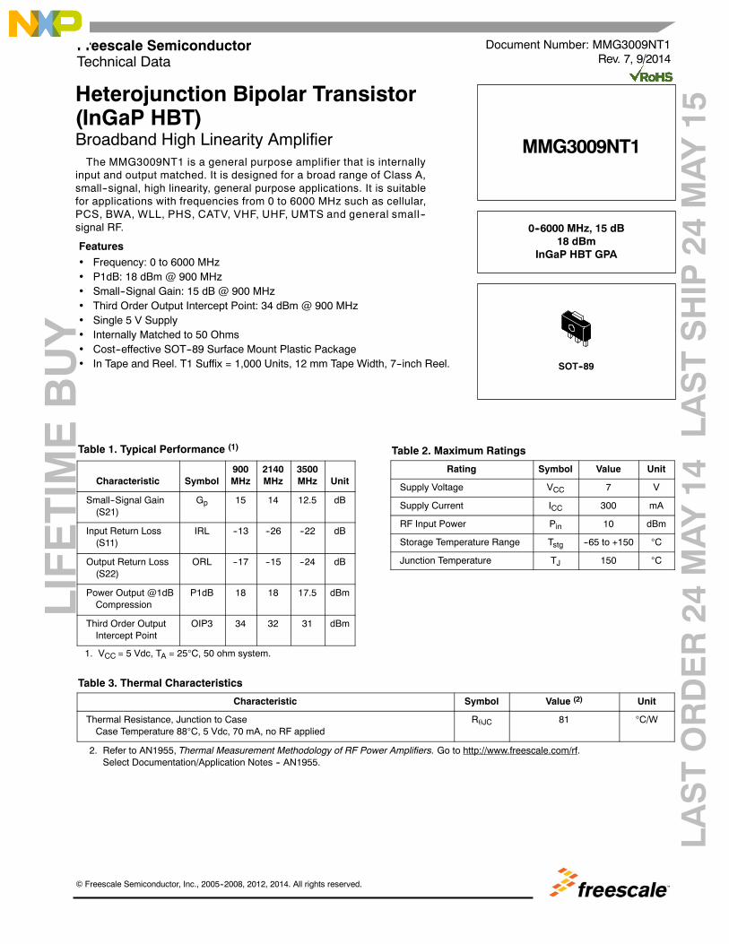
MMG3009NT1 0--6000 MHz, 15 dB 18 dBm InGaP HBT GPA Heterojunction Bipolar Transistor (InGaP HBT) Broadband High Linearity Amplifier The MMG3009NT1 is a general purpose amplifier that is internally input and output matched. It is designed for a broad range of Class A, small--signal, high linearity, general purpose applications. It is suitable for applications with frequencies from 0 to 6000 MHz such as cellular, PCS, BWA, WLL, PHS, CATV, VHF, UHF, UMTS and general small-- signal RF. Features Frequency: 0 to 6000 MHz P1dB: 18 dBm @ 900 MHz Small--Signal Gain: 15 dB @ 900 MHz Third Order Output Intercept Point: 34 dBm @ 900 MHz Single 5 V Supply Internally Matched to 50 Ohms Cost--effective SOT--89 Surface Mount Plastic Package In Tape and Reel. T1 Suffix = 1,000 Units, 12 mm Tape Width, 7--inch Reel. SOT--89 Table 1. Typical Performance (1) Characteristic Symbol 900 MHz 2140 MHz 3500 MHz Unit Small--Signal Gain (S21) G p 15 14 12.5 dB Input Return Loss (S11) IRL --13 --26 --22 dB Output Return Loss (S22) ORL --17 --15 --24 dB Power Output @1dB Compression P1dB 18 18 17.5 dBm Third Order Output Intercept Point OIP3 34 32 31 dBm 1. V CC = 5 Vdc, T A = 25C, 50 ohm system. Table 2. Maximum Ratings Rating Symbol Value Unit Supply Voltage V CC 7 V Supply Current I CC 300 mA RF Input Power P in 10 dBm Storage Temperature Range T stg --65 to +150 C Junction Temperature T J 150 C Table 3. Thermal Characteristics Characteristic Symbol Value (2) Unit Thermal Resistance, Junction to Case Case Temperature 88C, 5 Vdc, 70 mA, no RF applied R JC 81 C/W 2. Refer to AN1955, Thermal Measurement Methodology of RF Power Amplifiers. Go to http://www.freescale.com/rf . Select Documentation/Application Notes -- AN1955. LIFETIME BUY LAST ORDER 24 MAY 14 LAST SHIP 24 MAY 15 Document Number: MMG3009NT1 Rev. 7, 9/2014 Freescale Semiconductor Technical Data Freescale Semiconductor, Inc., 2005--2008, 2012, 2014. All rights reserved.
Transcript of Heterojunction Bipolar Transistor (InGaP HBT)
MMG3009NT1
1RF Device DataFreescale Semiconductor, Inc.
MMG3009NT1
0--6000 MHz, 15 dB18 dBm
InGaP HBT GPA
Heterojunction Bipolar Transistor(InGaP HBT)Broadband High Linearity AmplifierThe MMG3009NT1 is a general purpose amplifier that is internally
input and output matched. It is designed for a broad range of Class A,small--signal, high linearity, general purpose applications. It is suitablefor applications with frequencies from 0 to 6000 MHz such as cellular,PCS, BWA, WLL, PHS, CATV, VHF, UHF, UMTS and general small--signal RF.
Features Frequency: 0 to 6000 MHz P1dB: 18 dBm @ 900 MHz Small--Signal Gain: 15 dB @ 900 MHz Third Order Output Intercept Point: 34 dBm @ 900 MHz Single 5 V Supply Internally Matched to 50 Ohms Cost--effective SOT--89 Surface Mount Plastic Package In Tape and Reel. T1 Suffix = 1,000 Units, 12 mm Tape Width, 7--inch Reel. SOT--89
Table 1. Typical Performance (1)
Characteristic Symbol900MHz
2140MHz
3500MHz Unit
Small--Signal Gain(S21)
Gp 15 14 12.5 dB
Input Return Loss(S11)
IRL --13 --26 --22 dB
Output Return Loss(S22)
ORL --17 --15 --24 dB
Power Output @1dBCompression
P1dB 18 18 17.5 dBm
Third Order OutputIntercept Point
OIP3 34 32 31 dBm
1. VCC = 5 Vdc, TA = 25C, 50 ohm system.
Table 2. Maximum Ratings
Rating Symbol Value Unit
Supply Voltage VCC 7 V
Supply Current ICC 300 mA
RF Input Power Pin 10 dBm
Storage Temperature Range Tstg --65 to +150 C
Junction Temperature TJ 150 C
Table 3. Thermal Characteristics
Characteristic Symbol Value (2) Unit
Thermal Resistance, Junction to CaseCase Temperature 88C, 5 Vdc, 70 mA, no RF applied
RJC 81 C/W
2. Refer to AN1955, Thermal Measurement Methodology of RF Power Amplifiers. Go to http://www.freescale.com/rf.Select Documentation/Application Notes -- AN1955.
LIFETIMEBUY
LASTORDER24
MAY14
LASTSHIP
24MAY15
Document Number: MMG3009NT1Rev. 7, 9/2014
Freescale SemiconductorTechnical Data
Freescale Semiconductor, Inc., 2005--2008, 2012, 2014. All rights reserved.

2RF Device Data
Freescale Semiconductor, Inc.
MMG3009NT1
Table 4. Electrical Characteristics (VCC = 5 Vdc, 900 MHz, TA = 25C, 50 ohm system, in Freescale Application Circuit)
Characteristic Symbol Min Typ Max Unit
Small--Signal Gain (S21) Gp 14.3 15 — dB
Input Return Loss (S11) IRL — --13 — dB
Output Return Loss (S22) ORL — --17 — dB
Power Output @ 1dB Compression P1dB — 18 — dBm
Third Order Output Intercept Point OIP3 — 34 — dBm
Noise Figure NF — 4.2 — dB
Supply Current ICC 58 70 82 mA
Supply Voltage VCC — 5 — V
Table 5. Functional Pin Description
PinNumber Pin Function
1 RFin
2 Ground
3 RFout/DC Supply
Table 6. ESD Protection Characteristics
Test Methodology Class
Human Body Model (per JESD 22--A114) 1A
Machine Model (per EIA/JESD 22--A115) A
Charge Device Model (per JESD 22--C101) IV
Table 7. Moisture Sensitivity Level
Test Methodology Rating Package Peak Temperature Unit
Per JESD 22--A113, IPC/JEDEC J--STD--020 1 260 C
LIFETIMEBUY
LASTORDER24
MAY14
LASTSHIP
24MAY15
Figure 1. Functional Diagram
321
2

MMG3009NT1
3RF Device DataFreescale Semiconductor, Inc.
50 OHM TYPICAL CHARACTERISTICS
5
20
0
TC = 85C
f, FREQUENCY (GHz)
Figure 2. Small--Signal Gain (S21) versusFrequency
15
10
1 2 3 4
Gp,SM
ALL--SIGNAL
GAIN(dB) 25C
--40C
4--40
0
0
S11
f, FREQUENCY (GHz)
Figure 3. Input/Output Return Loss versusFrequency
S22
--10
--20
--30
1 2 3
S11,S22(dB)
20
7
21
10
Pout, OUTPUT POWER (dBm)
Figure 4. Small--Signal Gain versus OutputPower
19
17
15
13
11
12 14
9
3.532.521.510.513
20
19
18
16
14
f, FREQUENCY (GHz)
Figure 5. P1dB versus Frequency
P1dB,1dB
COMPRESSIONPOINT(dBm
)
17
15
5.40
100
4
VCC, COLLECTOR VOLTAGE (V)
Figure 6. Collector Current versus CollectorVoltage
80
60
20
4.2 5 5.2
I CC,COLLECTORCURRENT(mA)
40
4.4 4.6 4.8 421
36
0
f, FREQUENCY (GHz)
Figure 7. Third Order Output Intercept Pointversus Frequency
33
30
27
24
1 2 3
OIP3,THIRDORDER
OUTPUTINTERCEPTPOINT(dBm
)
1816
Gp,SM
ALL--SIGNAL
GAIN(dB)
VCC = 5 Vdc
900 MHz2140 MHz
1960 MHz
2600 MHz
3500 MHz
VCC = 5 Vdc
VCC = 5 Vdc VCC = 5 Vdc
VCC = 5 Vdc1 MHz Tone Spacing
LIFETIMEBUY
LASTORDER24
MAY14
LASTSHIP
24MAY15

4RF Device Data
Freescale Semiconductor, Inc.
MMG3009NT1
50 OHM TYPICAL CHARACTERISTICS
21
36
4.9
VCC, COLLECTOR VOLTAGE (V)
Figure 8. Third Order Output Intercept Pointversus Collector Voltage
33
30
27
24
OIP3,THIRDORDER
OUTPUTINTERCEPTPOINT(dBm
)
4.95 5 5.15.05
f = 900 MHz1 MHz Tone Spacing
100--40 --20 0 20 40 60 8028
35
T, TEMPERATURE (_C)
Figure 9. Third Order Output Intercept Pointversus Case Temperature
33
32
31
30
OIP3,THIRDORDER
OUTPUTINTERCEPTPOINT(dBm
)
29
Figure 10. Third Order Intermodulation Distortionversus Output Power
Pout, OUTPUT POWER (dBm)
IMD,THIRDORDER
INTERMODULATIONDISTORTION(dBc)
0 3 6 9 12--80
--30
--50
--60
--70
--40
150103
105
120
Figure 11. MTTF versus Junction Temperature
104
125 130 135 140 145
TJ, JUNCTION TEMPERATURE (C)
NOTE: The MTTF is calculated with VCC = 5 Vdc, ICC = 70 mA
MTTF(YEARS)
40
8
0
f, FREQUENCY (GHz)
Figure 12. Noise Figure versus Frequency
6
4
2
1 2 3
NF,NOISEFIGURE(dB)
--70
--20
2
Pout, OUTPUT POWER (dBm)
Figure 13. Single--Carrier W--CDMA AdjacentChannel Power Ratio versus Output Power
--30
--40
--50
--60
121084
ACPR,ADJACENTCHANNEL
POWER
RATIO(dBc)
14 16
34
6
VCC = 5 Vdcf = 900 MHz1 MHz Tone Spacing
15
VCC = 5 Vdc
VCC = 5 Vdc, f = 2140 MHzSingle--Carrier W--CDMA, 3.84 MHz Channel BandwidthInput Signal PAR = 8.5 dB @ 0.01% Probability (CCDF)
VCC = 5 Vdcf = 900 MHz1 MHz Tone Spacing
LIFETIMEBUY
LASTORDER24
MAY14
LASTSHIP
24MAY15

MMG3009NT1
5RF Device DataFreescale Semiconductor, Inc.
50 OHM APPLICATION CIRCUIT: 40--300 MHz
Figure 14. 50 Ohm Test Circuit Schematic
RFOUTPUT
RFINPUT
VSUPPLY
C3 C4
Z1 Z2
C1
Z5
C2
R1
L1
VCC
Z4Z3DUT
Figure 15. S21, S11 and S22 versus Frequency
--40
20
0
f, FREQUENCY (MHz)
S22
100 400 500
10
0
--10
--20
--30
Figure 16. 50 Ohm Test Circuit Component Layout
C1
L1
C2
R1
C4C3
Z1, Z5 0.347 x 0.058 MicrostripZ2 0.575 x 0.058 MicrostripZ3 0.172 x 0.058 Microstrip
Z4 0.403 x 0.058 MicrostripPCB Getek Grade ML200C, 0.031, r = 4.1
S21,S11,S22(dB)
S21
S11
200 300
MMG30XXRev 2
VCC = 5 Vdc
Table 8. 50 Ohm Test Circuit Component Designations and ValuesPart Description Part Number Manufacturer
C1, C2, C3 0.01 F Chip Capacitors C0603C103J5RAC Kemet
C4 1000 pF Chip Capacitor C0603C102J5RAC Kemet
L1 470 nH Chip Inductor BK2125HM471--T Taiyo Yuden
R1 0 Ω Chip Resistor ERJ3GEY0R00V Panasonic
LIFETIMEBUY
LASTORDER24
MAY14
LASTSHIP
24MAY15

6RF Device Data
Freescale Semiconductor, Inc.
MMG3009NT1
50 OHM APPLICATION CIRCUIT: 300--3600 MHz
Figure 17. 50 Ohm Test Circuit Schematic
RFOUTPUT
RFINPUT
VSUPPLY
C3 C4
Z1 Z2
C1
Z5
C2
R1
L1
VCC
Z4Z3DUT
Figure 18. S21, S11 and S22 versus Frequency
--30
30
f, FREQUENCY (MHz)
S22
800
20
10
0
--10
--20
Figure 19. 50 Ohm Test Circuit Component Layout
C1
L1
C2
R1
C4C3
Z1, Z5 0.347 x 0.058 MicrostripZ2 0.575 x 0.058 MicrostripZ3 0.172 x 0.058 Microstrip
Z4 0.403 x 0.058 MicrostripPCB Getek Grade ML200C, 0.031, r = 4.1
S21,S11,S22(dB)
S21
S11
1300300 1800 2300 2800 3300 3800
MMG30XXRev 2
VCC = 5 Vdc
Table 9. 50 Ohm Test Circuit Component Designations and ValuesPart Description Part Number Manufacturer
C1, C2 150 pF Chip Capacitors C0603C151J5RAC Kemet
C3 0.01 F Chip Capacitor C0603C103J5RAC Kemet
C4 1000 pF Chip Capacitor C0603C102J5RAC Kemet
L1 56 nH Chip Inductor HK160856NJ--T Taiyo Yuden
R1 0 Ω Chip Resistor ERJ3GEY0R00V Panasonic
LIFETIMEBUY
LASTORDER24
MAY14
LASTSHIP
24MAY15

MMG3009NT1
7RF Device DataFreescale Semiconductor, Inc.
50 OHM TYPICAL CHARACTERISTICS
Table 10. Common Emitter S--Parameters (VCC = 5 Vdc, TA = 25C, 50 Ohm System)
fMHz
S11 S21 S12 S22
|S11| |S21| |S12| |S22|
100 0.19606 --174.964 6.33492 175.897 0.10115 --0.614 0.07282 176.529
150 0.19734 --176.357 6.30368 173.26 0.10204 --1.587 0.07571 178.062
200 0.19944 169.849 6.27983 171.036 0.10220 --2.173 0.07648 --178.213
250 0.20027 168.421 6.24623 169.018 0.10243 --2.498 0.08038 --175.337
300 0.19924 166.435 6.22884 166.867 0.10334 --2.998 0.07928 --172.371
350 0.19543 164.497 6.22675 164.532 0.10364 --3.636 0.07836 --172.028
400 0.19419 162.266 6.21021 162.42 0.10357 --4.18 0.07876 --169.383
450 0.19172 160.135 6.19495 160.278 0.10351 --4.669 0.07882 --167.245
500 0.18914 158.072 6.18191 158.065 0.10361 --5.256 0.07903 --165.903
550 0.18788 156.056 6.16313 155.935 0.10378 --5.746 0.07946 --164.125
600 0.18596 154.01 6.14591 153.778 0.10379 --6.277 0.08061 --162.978
650 0.18399 152.064 6.12734 151.629 0.10396 --6.756 0.08181 --162.118
700 0.18285 150.008 6.10486 149.511 0.10408 --7.313 0.08346 --161.229
750 0.18159 148.088 6.08449 147.384 0.10411 --7.817 0.08496 --160.812
800 0.18056 146.09 6.06038 145.27 0.10427 --8.376 0.08717 --160.896
850 0.17973 144.286 6.03306 143.153 0.10440 --8.885 0.08917 --161.031
900 0.17932 142.485 6.00923 141.039 0.10453 --9.38 0.09202 --161.574
950 0.17920 140.759 5.98147 138.952 0.10467 --9.995 0.09484 --162.293
1000 0.17847 139.226 5.95646 136.927 0.10485 --10.462 0.09809 --163.293
1050 0.17754 137.531 5.92809 134.838 0.10508 --11.017 0.10057 --164.366
1100 0.17453 136.047 5.89423 132.763 0.10519 --11.541 0.10471 --165.489
1150 0.17205 134.871 5.86296 130.716 0.10534 --12.012 0.10843 --167.229
1200 0.17066 133.54 5.83017 128.685 0.10542 --12.612 0.11227 --168.9
1250 0.16951 132.305 5.79633 126.662 0.10564 --13.155 0.11601 --170.51
1300 0.16662 131.182 5.76557 124.647 0.10580 --13.654 0.12012 --172.32
1350 0.16577 130.038 5.73189 122.631 0.10602 --14.194 0.12430 --174.175
1400 0.16504 128.988 5.69605 120.653 0.10620 --14.728 0.12842 --176.041
1450 0.16426 128.206 5.65985 118.678 0.10641 --15.283 0.13238 --178.197
1500 0.16609 122.177 5.63288 116.712 0.10680 --15.856 0.13929 --178.349
1550 0.16661 120.535 5.60045 114.805 0.10706 --16.422 0.14264 179.292
1600 0.16797 118.895 5.56701 112.889 0.10732 --16.914 0.14623 176.482
1650 0.17042 117.389 5.53367 110.947 0.10761 --17.529 0.14778 174.032
1700 0.17177 116.114 5.50453 109.079 0.10790 --18.111 0.15034 171.358
1750 0.17361 114.897 5.47270 107.137 0.10818 --18.625 0.15223 168.855
1800 0.17663 113.75 5.43993 105.194 0.10841 --19.165 0.15382 166.27
1850 0.17969 112.634 5.40358 103.282 0.10863 --19.761 0.15575 163.924
1900 0.18333 111.562 5.36970 101.431 0.10919 --20.39 0.15708 161.656
1950 0.18634 110.534 5.33711 99.484 0.10950 --21.017 0.15722 159.517
2000 0.18991 109.707 5.30347 97.624 0.10980 --21.621 0.15781 157.67
2050 0.19272 108.497 5.26942 95.722 0.11012 --22.222 0.15859 156.162
2100 0.19593 107.602 5.23491 93.803 0.11037 --22.899 0.15951 154.73
2150 0.19925 106.721 5.19782 91.865 0.11076 --23.629 0.16086 153.761
2200 0.20272 105.922 5.15894 89.97 0.11107 --24.273 0.16242 152.923
2250 0.20521 104.933 5.11750 88.119 0.11132 --24.939 0.16412 151.958
(continued)
LIFETIMEBUY
LASTORDER24
MAY14
LASTSHIP
24MAY15

8RF Device Data
Freescale Semiconductor, Inc.
MMG3009NT1
50 OHM TYPICAL CHARACTERISTICS
Table 10. Common Emitter S--Parameters (VCC = 5 Vdc, TA = 25C, 50 Ohm System) (continued)
fMHz
S11 S21 S12 S22
|S11| |S21| |S12| |S22|
2300 0.20819 103.761 5.07836 86.232 0.11160 --25.64 0.16622 151.355
2350 0.21027 102.506 5.03981 84.384 0.11177 --26.346 0.16892 150.63
2400 0.21179 101.509 4.99976 82.526 0.11206 --26.995 0.17307 150.179
2450 0.21372 100.321 4.95674 80.649 0.11219 --27.627 0.17696 149.454
2500 0.21503 99.084 4.91517 78.813 0.11247 --28.368 0.18136 148.699
2550 0.21607 98.079 4.87557 77.083 0.11260 --29.056 0.18649 147.675
2600 0.21693 96.937 4.83415 75.317 0.11290 --29.737 0.19209 146.671
2650 0.21764 95.679 4.79330 73.409 0.11315 --30.261 0.19800 145.149
2700 0.21800 94.585 4.75322 71.62 0.11317 --31.061 0.20392 144.12
2750 0.21817 93.428 4.71387 69.917 0.11349 --31.733 0.20970 142.804
2800 0.21833 92.207 4.67702 68.159 0.11366 --32.454 0.21628 141.065
2850 0.21805 91.061 4.63817 66.317 0.11402 --33.132 0.22172 139.329
2900 0.21865 89.888 4.60218 64.555 0.11435 --33.832 0.22856 137.508
2950 0.21925 88.748 4.56625 62.873 0.11463 --34.552 0.23450 135.667
3000 0.21915 87.532 4.53210 61.144 0.11512 --35.281 0.24044 133.457
3050 0.22110 86.342 4.50064 59.382 0.11540 --36.033 0.24561 131.639
3100 0.22166 85.246 4.46608 57.613 0.11582 --36.792 0.25129 129.229
3150 0.22283 84.227 4.43647 55.954 0.11604 --37.437 0.25625 127.153
3200 0.22458 83.152 4.40552 54.104 0.11651 --38.235 0.26146 124.84
3250 0.22637 82.137 4.37427 52.337 0.11696 --38.955 0.26652 122.578
3300 0.22771 81.039 4.34455 50.582 0.11740 --39.776 0.27125 120.071
3350 0.23010 79.979 4.31085 48.824 0.11778 --40.645 0.27548 118.04
3400 0.23244 78.98 4.28183 47.09 0.11825 --41.441 0.28049 115.642
3450 0.23531 78.054 4.25137 45.379 0.11856 --42.323 0.28504 113.247
3500 0.23838 77.028 4.22125 43.528 0.11892 --43.156 0.28907 111.227
3550 0.24191 76.08 4.19033 41.795 0.11931 --43.953 0.29393 108.97
3600 0.24470 75.139 4.15822 40.059 0.11966 --44.868 0.29797 106.843
LIFETIMEBUY
LASTORDER24
MAY14
LASTSHIP
24MAY15

MMG3009NT1
9RF Device DataFreescale Semiconductor, Inc.
1.7
5.33
3.48
0.581.27
0.86
3.86
0.64
7.62
2.49
2.541.27
0.305 diameter
Figure 20. Recommended Mounting Configuration
NOTES:1. THERMAL AND RF GROUNDING CONSIDERATIONS SHOULD BE
USED IN PCB LAYOUT DESIGN.2. DEPENDING ON PCB DESIGN RULES, AS MANY VIAS AS
POSSIBLE SHOULD BE PLACED ON THE LANDING PATTERN.3. IF VIAS CANNOT BE PLACED ON THE LANDING PATTERN, THEN
AS MANY VIAS AS POSSIBLE SHOULD BE PLACED AS CLOSE TOTHE LANDING PATTERN AS POSSIBLE FOR OPTIMAL THERMALAND RF PERFORMANCE.
4. RECOMMENDED VIA PATTERN SHOWN HAS 0.381 x 0.762 MMPITCH.
Recommended Solder Stencil
Figure 21. Product Marking
M3009N( )
YYWWLIFETIMEBUY
LASTORDER24
MAY14
LASTSHIP
24MAY15

10RF Device Data
Freescale Semiconductor, Inc.
MMG3009NT1
PACKAGE DIMENSIONS

MMG3009NT1
11RF Device DataFreescale Semiconductor, Inc.
12RF Device Data
Freescale Semiconductor, Inc.
MMG3009NT1

MMG3009NT1
13RF Device DataFreescale Semiconductor, Inc.
PRODUCT DOCUMENTATION, SOFTWARE AND TOOLS
Refer to the following resources to aid your design process.
Application Notes
AN1955: Thermal Measurement Methodology of RF Power Amplifiers AN3100: General Purpose Amplifier and MMIC BiasingSoftware
.s2p FileDevelopment Tools
Printed Circuit Boards
For Software and Tools, do a Part Number search at http://www.freescale.com, and select the “Part Number” link. Go toSoftware & Tools on the part’s Product Summary page to download the respective tool.
REVISION HISTORY
The following table summarizes revisions to this document.
Revision Date Description
3 Mar. 2007 Corrected and updated Part Numbers in Tables 8 and 9, Component Designations and Values, to RoHScompliant part numbers, pp. 6, 7
4 July 2007 Replaced Case Outline 1514--01 with 1514--02, Issue D, pp. 1, 11--13. Case updated to add missingdimension for Pin 1 and Pin 3.
5 Mar. 2008 Removed Footnote 2, Continuous voltage and current applied to device, from Table 2, Maximum Ratings,p. 1
Corrected Fig. 13, Single--Carrier W--CDMA Adjacent Channel Power Ratio versus Output Power y--axis(ACPR) unit of measure to dBc, p. 5
Corrected S--Parameter table frequency column label to read “MHz” versus “GHz” and correctedfrequency values from GHz to MHz, pp. 8, 9
6 Feb. 2012 Corrected temperature at which ThetaJC is measured from 25C to 88C and added “no RF applied” toThermal Characteristics table to indicate that thermal characterization is performed under DC test with noRF signal applied, p. 1
Table 6, ESD Protection Characterization, removed the word “Minimum” after the ESD class rating. ESDratings are characterized during new product development but are not 100% tested during production. ESDratings provided in the data sheet are intended to be used as a guideline when handling ESD sensitivedevices, p. 3
Removed ICC bias callout from applicable graphs and Table 10, Common Emitter S--Parameters headingas bias is not a controlled value, pp. 4--9
Added .s2p File availability to Product Software and Printed Circuit Boards to Development Tools, p. 14
7 Sept. 2014 Added Fig. 21, Product Marking, p. 9
LIFETIMEBUY
LASTORDER24
MAY14
LASTSHIP
24MAY15

14RF Device Data
Freescale Semiconductor, Inc.
MMG3009NT1
Information in this document is provided solely to enable system and softwareimplementers to use Freescale products. There are no express or implied copyrightlicenses granted hereunder to design or fabricate any integrated circuits based on theinformation in this document.
Freescale reserves the right to make changes without further notice to any productsherein. Freescale makes no warranty, representation, or guarantee regarding thesuitability of its products for any particular purpose, nor does Freescale assume anyliability arising out of the application or use of any product or circuit, and specificallydisclaims any and all liability, including without limitation consequential or incidentaldamages. “Typical” parameters that may be provided in Freescale data sheets and/orspecifications can and do vary in different applications, and actual performance mayvary over time. All operating parameters, including “typicals,” must be validated foreach customer application by customer’s technical experts. Freescale does not conveyany license under its patent rights nor the rights of others. Freescale sells productspursuant to standard terms and conditions of sale, which can be found at the followingaddress: freescale.com/SalesTermsandConditions.
Freescale and the Freescale logo are trademarks of Freescale Semiconductor, Inc.,Reg. U.S. Pat. & Tm. Off. All other product or service names are the property of theirrespective owners.E 2005--2008, 2012, 2014 Freescale Semiconductor, Inc.
How to Reach Us:
Home Page:freescale.com
Web Support:freescale.com/support
Document Number: MMG3009NT1Rev. 7, 9/2014