HDSP F15x Series
11
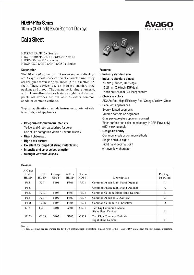
Features • Indus try st and ard siz e • Indu stry standard pinou t 7 .6 mm (0.3 inch) DIP si ngle 15.24 mm (0.6 inch) DIP dual Leads on 2.5 4 mm (0.1 inch) cent ers • Choice of colors AlGaAs Red, High Efficiency Red, Orange, Yellow, Green • E xcelle nt appearance Evenly lighted segments M itered corners on seg ments Gray package gives optimum contrast Black surface and color tinted epoxy (HDSP-F161 only) ±50° viewing angle • Desi gn flexibilit y Common anode or common cathode Single and dua l digit s Right hand decimal point ±1. ove rflow character HDSP-F15x/F16x Series HDSP-F20x/F30x/F40x/F50x Series HDSP-G00x/G15x Series HDSP-G20x/G30x/G40x/G50x Series AlGaAs Re d [1 ] HE R Or a n ge Y e l l ow Gree n P ack a ge HDS P - HDSP- HDS P - HDSP- HDSP- De s cr i p t i o n Dr a w in g F151 F201 F401 F301 F501 Common A node Right Hand Decimal A F161 Common A node Right Hand Decimal A F153 F203 F403 F303 F503 Common Cat hode Right Hand Decimal B F157 F207 F407 F307 F507 Common A node ± 1. Over flow C F158 F208 F408 F308 F508 Common Cat hode ± 1. Over flow D G151 G201 G401 G301 G501 Two Digit Common Anode Right Hand Decimal E G153 G203 G403 G303 G503 Two Digit Common Cathode Right Hand Decimal F Devices Note: 1. These displays are recommended for high ambient light operation. Please refer to the HDSP-F10X data sheet for low current operation. Description The 10 mm (0.40 inch) LED seven segment displays are Avago’s most space-efficient character size. They are designed for viewing distances up to 4.5 metres (1 5 feet). These devices use an industry standard size package an d pinout. The dual numeric, single numeric, an d ± 1. overflow devices feature a right hand decimal point. All devices are available as either common anode or common cathode. Typical applications include instruments, point of sale terminals, and app liances. • Catego rized f or lumin ou s intens ity Yellow and Green categorized for color Use o f l ike categories yields a uniform display • Hig h lig ht ou tput • Hi gh pe ak current • E xcellent fo r long digit string multiplexing • Intens ity and c olo r selectio n op tion • Sunlight viewable AlGaAs HDSP-F15x Series 10 mm (0. 40 i nch) S eve n S egment Di s pl ays D at a S heet
-
Upload
guillermo-hernandez -
Category
Documents
-
view
226 -
download
0
Transcript of HDSP F15x Series
8/4/2019 HDSP F15x Series
http://slidepdf.com/reader/full/hdsp-f15x-series 1/11
Features
• Industry standard size
• Industry standard pinout
7.6 mm (0.3 inch) DIP single
15.24 mm (0.6 inch) DIP dual
Leads on 2.54 mm (0.1 inch) centers
• Choice of colorsAlGaAs Red, High Efficiency Red, Orange, Yellow, Green
• Excellent appearance
Evenly lighted segments
Mitered corners on segments
Gray package gives optimum contrast
Black surface and color tinted epoxy (HDSP-F161 only)
±50° viewing angle
• Design flexibility
Common anode or common cathode
Single and dual digit s
Right hand decimal point±1. overflow character
HDSP-F15x/F16x Ser iesHDSP-F20x/F30x/F40x/F50x SeriesHDSP-G00x/G15x SeriesHDSP-G20x/G30x/G40x/G50x Series
AlGaAs
Red [1 ] HER Or ange Yellow Gr een Package
HDSP- HDSP- HDSP- HDSP- HDSP- Descr ipt ion Draw ing
F151 F201 F401 F301 F501 Common Anode Right Hand Decimal A
F161 Common Anode Right Hand Decimal A
F153 F203 F403 F303 F503 Common Cathode Right Hand Decimal B
F157 F207 F407 F307 F507 Common Anode ± 1. Overflow C
F158 F208 F408 F308 F508 Common Cathode ± 1. Overflow D
G151 G201 G401 G301 G501 Two Digit Common Anode
Right Hand Decimal E
G153 G203 G403 G303 G503 Two Digit Common Cathode
Right Hand Decimal F
Devices
Note:1. These displays are recommended for high ambient light operation. Please refer to the HDSP-F10X data sheet for low current operation.
Description
The 10 mm (0.40 inch) LED seven segment displays
are Avago’s most space-efficient character size. They
are designed for viewing distances up to 4.5 metres (15
feet). These devices use an industry standard size
package and pinout. The dual numeric, single numeric,
and ± 1. overflow devices feature a right hand decimal
point. All devices are available as either commonanode or common cathode.
Typical applications include instruments, point of sale
terminals, and app liances.
• Categorized for luminous intensity
Yellow and Green categorized for color
Use of l ike categories yields a uniform display
• High light output
• High peak current
• Excellent for long digit string multiplexing• Intensity and color selection option
• Sunlight viewable AlGaAs
HDSP-F15x Series10 mm (0.40 inch) Seven Segment Displays
Data Sheet

8/4/2019 HDSP F15x Series
http://slidepdf.com/reader/full/hdsp-f15x-series 2/11
2
Part N umbering System
5 0 8 2 - x xx x - x x x xx
HDSP - x xx x - x x x xx
Mechanical Options [1]
00: No mechan ical option
16: Special dimensional tolerances
Color Bin Options [1,2]
0: No color bin limitation
Maximum Intensity Bin [1,2]
0: No ma ximu m int ensity bin limitation
Minimu m Intensity Bin [1,2]
0: No minimu m int ensity bin limitation
Device Configuration/Color[1]
1: Comm on Anode
3: Common Cath ode
Device Sp ecif ic Configuration [1]
Refer t o respective data sheet
Package [1 ]
F: 10 mm (0.4 inch) Single Digit Seven Segment Display
G: 10 mm (0.4 inch) Dual Digit Seven Segment Display
N ot es :
1. For codes not listed in the figure above, please r efer t o the respective data sheet or contact your near est Avago represent ative
for details.
2. Bin options r efer t o shippable bins for a par t-number. Color a nd Int ensity Bins are typically restricted to 1 bin per tube
(exceptions may apply). Please refer to respective data sheet for specific bin limit information.

8/4/2019 HDSP F15x Series
http://slidepdf.com/reader/full/hdsp-f15x-series 3/11
3
Package Dimensions

8/4/2019 HDSP F15x Series
http://slidepdf.com/reader/full/hdsp-f15x-series 4/11
4
FUNCTION
PIN E F
1 E CATHODE NO. 1 E ANODE NO. 12 D CATHODE NO. 1 D ANODE NO. 1
3 C CATHODE NO. 1 C ANODE NO. 1
4 DP CATHODE NO. 1 DP ANODE NO. 1
5 E CATHODE NO. 2 E ANODE NO. 2
6 D CATHODE NO. 2 D ANODE NO. 2
7 G CATHODE NO. 2 G ANODE NO. 2
8 C CATHODE NO. 2 C ANODE NO. 2
9 CP CATHODE NO. 2 DP ANODE NO. 2
10 B CATHODE NO. 2 B ANODE NO. 2
11 A CATHODE NO. 2 A ANODE NO. 2
12 F CATHODE NO. 2 F ANODE NO. 2
13 DIGIT NO. 2 ANODE DIGIT NO. 2 CATHODE
14 DIGIT NO. 1 ANODE DIGIT NO. 1 CATHODE
15 B CATHODE NO. 1 B ANODE NO. 1
16 A CATHODE NO. 1 A ANODE NO. 1
17 G CATHODE NO. 1 G ANODE NO. 1
18 F CATHODE NO. 1 F ANODE NO. 1
FUNCTION
PIN A B C D
1 ANODE[1] CATHODE[2] ANODE[1] CATHODE[2]
2 CATHODE f ANODE f CATHODE PLUS ANODE PLUS
3 CATHODE g ANODE g CATHODE MINUS ANODE MINUS
4 CATHODE e ANODE e NC NC
5 CATHODE d ANODE d NC NC
6 ANODE[1] CATHODE[2] ANODE[1] CATHODE[2]
7 CATHODE DP ANODE DP CATHODE DP ANODE DP
8 CATHODE c ANODE c CATHODE c ANODE c
9 CATHODE b ANODE b CATHODE b ANODE b
10 CATHODE a ANODE a NC NC
NOTES:1. REDUNDANT ANODES2. REDUNDANT CATHODES
Internal Circuit Diagram
HOLE PATTERN FOR PCB LAYOUT TO ACHIEVE UNIFORM 0.450 IN. DIGIT TO DIGIT PITCH. FOR HDSP-FXXX TO HDSP-GXXX.

8/4/2019 HDSP F15x Series
http://slidepdf.com/reader/full/hdsp-f15x-series 5/11
5
Electrical/ Optical Characteristics at TA
= 25°C
Notes:1. See Figure 1 to establish pulsed conditions.2. Derate above 46°C at 0.54 mA/ °C.3. See Figure 6 to establish pulsed conditions.4. Derate above 53°C at 0.45 mA/ °C.5. See Figure 7 to establish pulsed conditions.
6. Derate above 81°C at 0.52 mA/ °C.7. See Figure 8 to establish pulsed conditions.8. Derate above 39°C at 0.37 mA/ °C.9. For operation below -20°C, contact your local Avago
components sales office or an authorized distributor.
Device
Ser ies Par amet er Symbol Min. Typ. Max. Unit s Test Condit ions
Luminous Intensity/Segment[1,2,5] IV 7.5 15.0 mcd IF = 20 mA (Digit Average )
Forward Voltage/Segment or DP VF 1.8 2.2 V IF = 20 mA
HDSP- Peak Wavelength λPEAK 645 nm
F15x/
F16 x/ Dominant Wavelength[3] λd 637 nm
G15x
Reverse Voltage/Segment or DP[4] VR 3.0 15 V IR = 100 µA
Temperatur e Coefficient of ∆VF / °C -2 mV/ °C
VF /Segment or DP
Thermal Resistance LED RθJ-PIN 320 °C/W/Seg
Junction-to-Pin
AlGaAs Red
Absolute M aximum Ratings
AlGaAs Red HER/Orange Yellow Green
HDSP- HDSP- HDSP- HDSP-
F15x/F16x F20x/G20x/ F30x/G30x F50x/G50x
Descr ipt ion G15x Ser ies G40x Ser ies Ser ies Ser ies Unit s
Average Power per Segment or DP 96 105 80 105 mW
Peak Forward Current per 160[1] 90 [3] 60 [5 ] 90 [7 ] mASegment or DP
DC Forward Current per Segment 40[2] 30 [4] 20 [6 ] 30 [8 ] mA
or DP
Op erating Temp erature Range –20 to + 10 0[9 ] –40 to + 100 °C
Storage Temperature Range –55 to + 100 °C
Reverse Voltage per Segment or DP 3.0 V
Wavesoldering Temperature for 250 °C3 Seconds (1.59 mm [0.063 in.]
below body)

8/4/2019 HDSP F15x Series
http://slidepdf.com/reader/full/hdsp-f15x-series 6/11
6
Device
Ser ies Paramet er Symbol Min. Typ. Max. Unit s Test Condit ions
Luminous Intensity/Segment[1,2] IV 420 1200 µcd IF = 5 mA
(Digit Average )
Forward Voltage/Segment or DP VF 2.0 2.5 V IF = 20 mA
HDSP- Peak Wavelength λPEAK 635 nm
F20x/
G20 x Dominant Wavelength[3] λd 626 nm
Reverse Voltage/Segment or DP[4] VR 3.0 30 V IR = 100 µA
Temperatur e Coefficient of ∆VF / °C -2 mV/ °C
VF /Segment or DP
Thermal Resistance LED RθJ-PIN 320 °C/W/Seg
Junction-to-Pin
High Efficiency Red
Electrical/ Optical Characteristics at TA
= 25°C, continued
Orange
Device
Ser ies Paramet er Symbol Min. Typ. Max. Unit s Test Condit ions
Luminous Intensity/Segment[1,2] IV
420 1200 µcd IF
= 5 mA (Digit Average)
Forward Voltage/Segment or DP VF
2.0 2.5 V IF
= 20 mA
Peak Wavelength lPEAK
600 nm
Dominant Wavelength[3] ld
603 nm
Reverse Voltage/Segment or DP [4] VR
3.0 30 V IR
= 100 µA
Temperatur e Coefficient of ∆VF / °C -2 mV/ °C
VF /Segment or DP
Thermal Resistance LED Rl\qJ-PIN
320 °C/W/Seg
Junction-to-Pin
HDSP-
F40x/
G40x
8/4/2019 HDSP F15x Series
http://slidepdf.com/reader/full/hdsp-f15x-series 7/11
7
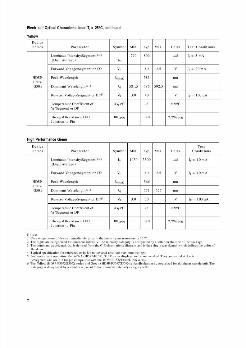
Yellow
Device
Ser ies Paramet er Symbol Min. Typ. Max. Unit s Test Condit ions
Luminous Intensity/Segment[1,2] 290 800 µcd IF = 5 mA
(Digit Average) IV
Forward Voltage/Segment or DP VF 2.2 2.5 V IF = 20 mA
HDSP- Peak Wavelength λPEAK 583 nm
F30x /
G30 x Dominant Wavelength[3,6] λd 581.5 586 592.5 nm
Reverse Voltage/Segment or DP[4] VR 3.0 40 V IR = 100 µA
Temperatur e Coefficient of ∆VF / °C -2 mV/ °C
VF /Segment or DP
Thermal Resistance LED RθJ-PIN 320 °C/W/Seg
Junction-to-Pin
High Performance Green
Notes:1. Case temperature of device immediately prior to the intensity measurement is 25°C.2. The digits are categor ized for luminous intensity. The intensity category is designated by a letter on t he side of the pac kage.3. The dominant wavelength, λd, is derived from the CIE chrom aticity diagram and is tha t single wavelength which defines the color of
the device.4. Typical specification for reference on ly. Do not exceed absolute maximum ra tings.5. For low current ope ration, the AlGaAs HDSP-F10X, G10X series displays are r ecommend ed. They are te sted at 1 mA
dc/segment a nd are pin for pin comp atible with the HDSP-F15X/F16x/G15X series.6. The Yellow (HDSP-F30X/G30X) s eries a nd Gree n ( HDSP-F50X/G50X) s eries displays ar e c ategorized for dominant wavelength. The
category is designated by a number adjacent to the luminous intensity category letter.
Device Test
Ser ies Par amet er Symbol Min. Typ. Max. Unit s Condit ions
Luminous Intensity/Segment[1,2] IV 1030 3500 µcd IF = 10 mA (Digit Average )
Forward Voltage/Segment or DP VF 2.1 2.5 V IF = 10 mA
HDSP- Peak Wavelength λPEAK 566 nmF50x /
G50 x Dominant Wavelength[3,6] λd 571 577 nm
Reverse Voltage/Segment or DP[4] VR 3.0 50 V IR = 100 µA
Temperatur e Coefficient of ∆VF / °C -2 mV/ °C
VF /Segment or DP
Thermal Resistance LED RθJ-PIN 320 °C/W/Seg
Junction-to-Pin
Electrical/ Optical Characteristics at TA
= 25°C, continued

8/4/2019 HDSP F15x Series
http://slidepdf.com/reader/full/hdsp-f15x-series 8/11
8
Figure 4. Relative Luminous Inte nsity vs. DC
Forward Current .
Figure 5. Relative E fficiency (Luminous Intensity
per Uni t Current ) vs . Peak Current .
AlGaAs Red
Figure 1. Maximum Tolera ble Peak Curr ent vs. Pulse
Dura tion – AlGaAs Red.
Figure 2. Maximum Allowable DC Curre nt vs.
Ambient Temperatur e.
Figure 3. Forward Cur rent vs. Forw ard Voltage.
I D C M A X . – M A X I M U M D C C U R R E N T
P E R S E G M E N T – m A
20
0
TA – AMBIENT TEMPERATURE – °C
30 90 120
50
30
7050
AlGaAs RED
10
20
5
15
25
35
40 60 80 100 110
40
45
RθJ-A = 770°C/W
I F – F O R W A R D C U R R E N T P E R S E G M E N T – m A
00
VF – FORWARD VOLTAGE – V
160
100
60
2.0 4.0
80
20
1.0 3.0
40
AlGaAs RED
0.5 1.5 2.5 3.5
120
140
R E L A T I V E L
U M I N O U S I N T E N S I T Y
( N O R M A L I
Z E D T O 1 A T 2 0 m A )
0
0
IF – FORWARD CURRENT PER SEGMENT – mA
2.00
1.50
1.25
0.75
0.25
20 40
1.75
1.00
0.50
10 305 15 25 35
AlGaAs RED
1.4
0.5
IPEAK – PEAK FORWARD CURRENT
PER SEGMENT – mA
0.6
0.8
1.0
1.2
150.05.0 50.0 η P E A K – N O R M A L I Z E D R E L A T I V E E F F I C I E N C Y
( N O R M A L I Z E D T O 1 A T 2 0 m A )
2.0
1.0 3.0
20.010.0
30.0 100.0
500.0
AlGaAs RED

8/4/2019 HDSP F15x Series
http://slidepdf.com/reader/full/hdsp-f15x-series 9/11
9
HER, Orange, Yellow, Green
Figure 6. Maximum Tolerable Pe ak Curre nt vs.
Pulse Durat ion – HER, Orange.
Figure 7. Maximum Tolerable Pea k Current vs.
Pulse Duration – Yellow.
Figure 10. Forward Current vs.
Forw ard Voltage Character ist ics.
Figure 11. Relative Luminous Int ensity
vs. DC Forward Current .
Figure 8. Maximum Tolerable Pea k Current
vs. Pulse Dura tion – Green.
Figure 9. Maximum Allowable DC Curre nt
vs. Ambient Temperature.
Figure 12. Relative Efficiency (Luminous
Intensity per Unit Current ) vs. Peak
Current .
8/4/2019 HDSP F15x Series
http://slidepdf.com/reader/full/hdsp-f15x-series 10/11
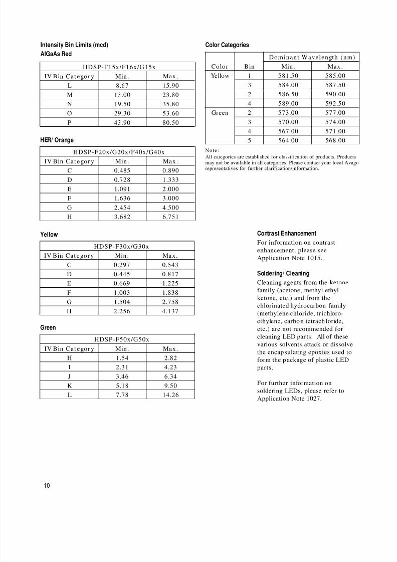
Intensity Bin Limits (mcd)
AlGaAs Red
HDSP-F15x/F16x/G15x
IV Bin Cat egor y Min. Max.
L 8.67 15.90
M 13.00 23.80
N 19.50 35.80
O 29.30 53.60
P 43.90 80.50
HDSP-F20x/G20x/F40x/G40x
IV Bin Cat egor y Min. Max.
C 0.485 0.890
D 0.728 1.333
E 1.091 2.000
F 1.636 3.000
G 2.454 4.500
H 3.682 6.751
HER/ Orange
HDSP-F30x/G30x
IV Bin Cat egor y Min. Max.
C 0.297 0.543
D 0.445 0.817
E 0.669 1.225
F 1.003 1.838G 1.504 2.758
H 2.256 4.137
Yellow
HDSP-F50x/G50x
IV Bin Cat egor y Min. Max.
H 1.54 2.82
I 2.31 4.23
J 3.46 6.34
K 5.18 9.50
L 7.78 14.26
Green
Dominant Wavelength (nm)
Color Bin Min. Max .
Yellow 1 581.50 585.00
3 584.00 587.50
2 586.50 590.00
4 589.00 592.50
Green 2 573.00 577.00
3 570.00 574.00
4 567.00 571.00
5 564.00 568.00
Color Categories
Note:
All categories are established for classification of products. Productsmay not be available in all categories. Please contact your local Avagorepresentatives for further clarification/information.
Contrast Enhancement
For information on contrast
enhancement, please see
Application Note 1015.
Soldering/ Cleaning
Cleaning agents from the ketone
family (acetone, methyl ethyl
ketone, etc.) and from the
chlorinated hydrocarbon family
(methylene chloride, tr ichloro-
ethylene, carbon tetrach loride,
etc.) are not recommended for
cleaning LED par ts. All of these
various solvents attack or dissolve
the encapsulating epoxies used to
form the p ackage of plastic LED
parts.
For further information on
soldering LEDs, please refer toApplication Note 1027.
10

8/4/2019 HDSP F15x Series
http://slidepdf.com/reader/full/hdsp-f15x-series 11/11
For product information and a complete list of distributors, please go to our website: www.avagotech.com
Avago, Avago Technologies, and the A logo are t rademarks of Avago Technologies Limit ed in t he United States and other countries.
Data subject t o change. Copyright © 2006 Avago Technologies Limited. All rights reserved. Obsoletes 5988-2222EN
5989-2346EN June 23, 2006


![Hammerfall DSP System HDSP AES-32 - …1].pdfHammerfall® DSP System HDSP AES-32 ... 30.8 Connector Pinouts ... BO25MXLR4M4F3 Digital breakout cable AES/EBU, 9.9 ft (3 m)](https://static.fdocuments.us/doc/165x107/5afa5a047f8b9a2d5d8e29b2/hammerfall-dsp-system-hdsp-aes-32-1pdfhammerfall-dsp-system-hdsp-aes-32.jpg)