Hashemi Dissertation - HARVEST
192
DESIGN, MICROFABRICATION, AND TESTING OF ALL-PMMA, NANOPORE-BASED ELECTROPHORETIC FLOW DETECTORS FOR BIOMEDICAL APPLICATIONS A Thesis Submitted to the College of Graduate Studies and Research in Partial Fulfillment of the Requirements for the Degree of Doctor of Philosophy in the Department of Electrical and Computer Engineering University of Saskatchewan Saskatoon, Saskatchewan by MANOUCHEHR HASHEMI © Copyright Manouchehr Hashemi, May 2014. All rights reserved.
Transcript of Hashemi Dissertation - HARVEST
DESIGN, MICROFABRICATION, AND TESTING OF
ALL-PMMA, NANOPORE-BASED
ELECTROPHORETIC FLOW DETECTORS
FOR BIOMEDICAL APPLICATIONS
A Thesis Submitted to the
College of Graduate Studies and Research
in Partial Fulfillment of the Requirements for the Degree of
Doctor of Philosophy
in the Department of Electrical and Computer Engineering
University of Saskatchewan
Saskatoon, Saskatchewan
by
MANOUCHEHR HASHEMI
© Copyright Manouchehr Hashemi, May 2014. All rights reserved.

i
PERMISSION TO USE
In presenting this thesis in partial fulfillment of the requirements for a Postgraduate
degree from the University of Saskatchewan, I agree that the Libraries of this University may
make it freely available for inspection. I further agree that permission for copying of this thesis
in any manner, in whole or in part, for scholarly purposes may be granted by the professor or
professors who supervised my thesis work or, in their absence, by the Head of the Department or
the Dean of the College in which my thesis work was done. It is understood that any copying or
publication or use of this thesis or parts thereof for financial gain shall not be allowed without
my written permission. It is also understood that due recognition shall be given to me and to the
University of Saskatchewan in any scholarly use which may be made of any material in my
thesis.
Requests for permission to copy or to make other use of material in this thesis in whole or in part
should be addressed to:
Head of the Department of Electrical and Computer Engineering
University of Saskatchewan
3B48 Engineering Building
57 Campus Drive, Saskatoon, SK
S7N 5A9

ii
ABSTRACT
Detection of and discrimination between different nanoparticles and biomolecules are vital
steps in analytical, biochemical, and diagnostic biomedical procedures used in life sciences.
Synthetic micro/nanopores in solid-state membranes form an emerging class of single-molecule
detectors capable of detecting and probing the properties of particles and biomolecules with high
throughput and resolution: The particles or biomolecules to be analyzed are added to an
electrolyte solution in one of the two reservoirs of the detector system separated by a thin
membrane containing a single micro/nanopore. An outer electric field induces an open-pore ionic
current (Iopen) through the pore, dragging the particles with itself. Transient changes occur when
a particle slightly smaller than the pore translocates through the pore. This electrical signal can
be analyzed to derive information regarding to the particle or biomolecule size and even its
morphology, concentration in the solution, and the affinity for the pore. Many detectors are
based on self-assembled, naturally occurring protein pores in lipid bilayer membranes. Most
solid-state pore-based detectors reported in literature use artificial pores in silicon nitride or
silicon oxide membranes. Applying polymers as a membrane potentially offers advantages over
the aforementioned types, including good electrical insulation, improved wettability thanks to
higher hydrophilicity, and long-term stable yet low-cost and disposable devices. The present
study aims at exploiting such advantages by developing the proof-of-concept for a single-
material, all-polymer, nanopore detector allowing the continuous variation of target pore size in
the range from micrometers to a few nanometers for best pore size adaption to the biomolecules
to be investigated. The research comprises materials selection, system design, development of a
fabrication and assembly sequence, device fabrication, and functional device testing. Poly

iii
(methyl methacrylate) (PMMA) was selected as it combines advantageous microfluidic
properties know from competing materials, such as polyimide, polystyrene, polycarbonate, or
polyethylene terephthalate, with outstanding micropatterning capabilities. The membrane
thickness is set to be 1 µm, based on a compromise between robustness during fabrication and
operation on one side, and electrochemical performance on the other. After spincoating the
membrane onto a sacrificial wafer, pores with diameters of typically several hundred nanometers
are patterned by electron beam lithography. In combination with thermal post processing leading
to polymer reflow, diameters one order of magnitude smaller can be achieved. The present study
focuses on 450 nm and 22 nm pores, respectively. Besides these pores fabricated in a top-down
approach, self-assembled -hemolysin protein pores of 1.5 nm diameter are integrated in a
combined top-down and bottom-up approach so that single digit, double digit, and triple digit
nanometer pores are available. Systems integration is achieved by capillary-forced based release
from the sacrificial substrate and the application of UV-initiated glue.
Test sequences proved and qualified the device functionality: Electrical characterization was
performed in aqueous KCl electrolyte solution. The devices exhibit a stable, time-independent
ionic current. The current-voltage curves are linear and scale with the electrolyte concentration.
System verification was performed using silica nanospheres of 100 nm and 150 nm diameter as
known test particles. Translocation through a 450 nm pore induced current blockades for about
1 ms with an amplitude of 30 pA to 55 pA for 100 nm particles and in excess of 70 pA for
150 nm particles. This is in close agreement with results obtained by a mathematical model used
in this study. Biomolecules relevant to many life science applications, double-stranded DNA
(dsDNA) and bovine serum albumin (BSA) were subsequently analyzed to prove the device
concept. Post-processed pores of 22 nm diameter were used at 600 mV driving voltage and

iv
0.1 molar electrolyte in a slightly acidic regime of pH = 6. Typical current blockade amplitudes
for complete translocations of dsDNA are Iblock = 22 pA for a translocation time of tD = 0.2 ms,
and an almost threefold current blockade (Iblock = 60 pA) for the larger BSA molecules,
respectively. The results demonstrate that the PMMA-based nanopores are sensitive enough to
not only detect translocating biomolecules, but to also sense them by distinguishing between
different biomolecules.
The molecule-specific and distinct translocation signals through the pores using both,
standardized silica nanoparticles and biomolecules of different dimensions, prove the concept of
an all-PMMA electrophoretic flow detector with adjustable pore diameters. Devices with pore
diameters covering three orders of magnitude in the nanometer range were successfully built,
tested, and characterized. The results suggest such detectors are promising candidates for
biomolecule detecting applications.

v
ACKNOWLEDGMENTS
First of all, I am greatly indebted to my supervisor, Dr. Sven Achenbach, for his constant
support, great guidance, valuable suggestions, and encouragements extended throughout the
course of my study, without which this thesis would not have been possible. His mentorship and
support had a great impact on both my study and life, and made my past years a very special
time.
I would like to take this opportunity to express my gratitude to my committee members Dr.
David Klymyshyn, Dr. Anh van Dinh, Dr. Li Chen, and Dr. Kevin Stanley for their support, time
and consideration in reading my thesis, and for their advice in defining and completing my
thesis.
I also sincerely thank the support and assistance provided by Garth Wells during my detector
device fabrication and experimentation period at TRTechs and the Synchrotron Laboratory for
Micro and Nano Devices (SyLMAND) at the Canadian Light Source (CLS). I would like to
appreciate all the personnel of the Edmonton NanoFAB Lab at the University of Alberta in
Canada, as well as the personnel of the Institute for Microstructure Technology (IMT) at the
Karlsruhe Institute for Technology (KIT) in Karlsruhe, Germany, for their contributions towards
making the fabrication of my polymer-based electrophoretic flow detector device possible.
I acknowledge the financial assistance for this project provided by the Natural Sciences and
Engineering Research Council of Canada (NSERC) and TRTechs. I also appreciate the Travel
grant provided by the College of Engineering, Department of Electrical Engineering and
Computer Science at the University of Saskatchewan (U of S), as it provided me a wonderful
experience and enhanced my graduate knowledge immensely.

vi
Last, but not least, I would like to thank my family for being always there for me. In
particular, I appreciate my wife, Banafsheh Moazed and my son, Arian, for their kind support,
love, patience, understanding, and self-sacrifice. Special thanks go to my parents, Ashraf and
Abolhassan, who deserve a very special mention. Finally, I would like to thank my sisters,
Farahnaz, Farzaneh, and Raheleh for their patience, understanding, and encouragements during
my program of study.

vii
TABLE OF CONTENTS
PERMISSION TO USE i
ABSTRACT ii
ACKNOWLEDGMENTS v
TABLE OF CONTENTS vii
LIST OF FIGURES xi
LIST OF TABLES xv
LIST OF ABBREVIATIONS xvi
LIST OF VARIABLES xix
1. Introduction 1
1.1. Motivation.....................................................................................................................1
1.2. Overview of DNA and Protein Structures.... ............................................................... 2
1.3. Review of Conventional Detection Methods for Cells and Biomolecules .................. 6
1.4. Review of Pore-Based Detection Methods for Cells and Biomolecules ..................... 9
1.4.1. Coulter Counter............................................................................................... 9
1.4.2. Miniaturized Electrophoretic Flow Detectors: Natural Protein
Nanopores......................................................................................................15
1.4.3. Miniaturized Electrophoretic Flow Detectors: Artificial
Micro/Nanopores...........................................................................................18

viii
1.5. Review of Fabrication Processes for Micro/Nanopores.............................................21
1.6. Objectives...................................................................................................................23
1.7. Thesis Organization....................................................................................................24
2. Theory of an All-PMMA Electrophoretic Flow Detector 26
2.1. Membrane mechanical Properties and Design Limitation..........................................27
2.2. Surface Energy Density Model applied for Post Processing of the Pore
to fine tune to the Diameter.........................................................................................33
2.3. Theoretical Model for the Electrophoretical Derivation of Pore
Dimensions.................................................................................................................35
2.4. Deblois Resistance Variance Model for Analytical Predictions of
Electrophoretic Current Blockades.............................................................................37
3. Design of an All-PMMA Electrophoretic Flow Detector 45
3.1. Material Selection.......................................................................................................45
3.1.1. Membrane......................................................................................................45
3.1.2. Detector System.............................................................................................51
3.2. Geometry of the micropatterned Membrane...............................................................52
3.2.1. Membrane Dimensions..................................................................................52
3.2.2. Pore Dimensions and Shape..........................................................................58
3.2.3. Auxiliary Components of the Detector Device.............................................61

ix
4. Fabrication Procedure and Detector Integration 65
4.1. Pore Fabrication by Electron Beam Lithography.......................................................65
4.1.1. Fine tuning the Diameter of Single Pores......................................................70
4.2. Fabrication of Auxiliary Device Components............................................................72
4.3. Detector System Integration........................................................................................72
4.4. Self-Assembly of α-hemolysin Protein Pores.............................................................79
5. Detector Test Results and Discussion 83
5.1. Patch Clamp Test Setup..............................................................................................83
5.2. Characterization of the Pore Geometry.......................................................................85
5.3. Analysis of the Open Pore Current.............................................................................87
5.3.1. Noise Level of unpatterned Membranes........................................................87
5.3.2. Long-Term Stability, Noise Level, and Repeatability of the
Open Pore Current.........................................................................................88
5.3.3. Current-Voltage Characteristics....................................................................93
5.3.4. Impact of the Electrolyte Concentration on the Open Pore Current
and the Cross-Pore Conductance..96
5.3.5. Impact of the Electrolyte Concentration on the Pore Resistance...................99
5.4. Functional Analysis of Submicron Pores via Translocation of
Differently-Sized Silica Nanoparticles.....................................................................100
5.4.1. Mathematical Model for the Current Blockade...........................................101

x
5.4.2. Measured Current Blockade of 100 nm Silica Nanoparticles......................103
5.4.3. Measured Current Blockade of 150 nm Silica Nanoparticles......................109
5.4.4. Comparison of modeled and measured Current Blockade..........................110
5.5. Functional Analysis of Self-Assembled Protein Pores via Translocation
of Linear ssDNA Molecules.....................................................................................112
5.6. Detection and Identification of Biomolecules..........................................................115
5.6.1. Factors impacting the Translocation of dsDNA Molecules........................117
5.6.2. Translocation Dynamics of dsDNA Molecules...........................................126
5.6.3. Translocation and Translocation Dynamics of BSA
Protein Molecules........................................................................................133
5.6.4. Discrimination of, and Differentiation between, Translocation
of dsDNA and BSA Biomolecules..............................................................145
6. Conclusion 149
6.1. Summary and Conclusions.......................................................................................149
6.2. Future Work..............................................................................................................152
REFERENCES 154

xi
LIST OF FIGURES
1.1 Schematic of the double-helical structure of double-stranded deoxy-ribonucleic
acid (dsDNA).........................................................................................................................4
1.2 Schematic of the structure of a protein molecule...................................................................5
1.3 Schematic representation of a Coulter counter device.........................................................10
1.4 Schematic illustration of an electrophoretic flow detector device.......................................13
1.5 Schematic representation of single-stranded DNA sequencing...........................................15
1.6 Schematic representation of an α-hemolysin protein pore...................................................16
2.1 Schematic layout of Electrophoretic Detector System.........................................................26
2.2 Discretization model in isometric view: Schematic of the membrane mesh used
for the 2D FEM simulation..................................................................................................29
2.3 Schematic of the constraints for the membrane in isometric view......................................30
2.4 Illustration of geodetic pressure evenly applied to one side of the membrane....................31
2.5 Simulation of von Mises stress resulting from a uniform pressure of 36 Pa
in a PMMA membrane with a diameter of 1 mm and a thickness of 250 nm......................32
2.6 Schematic of the cross section of a pore with a non-conducting sphere
and electric field lines...........................................................................................................39
3.1 Molecular structure of methyl methacrylate, the monomer of PMMA................................50
3.2 Simulated von Mises stress for a PMMA membrane with 1 mm diameter and
265 nm thickness under a pressure of 36 Pa.........................................................................54
3.3 Impact of varied geometric parameters on the simulated maximum Von Mises
stress in a PMMA membrane under the geodetic pressure of 3.68 mm electrolyte.............55

xii
3.4 Simulated distribution of von Mises stress in an unpatterned PMMA membrane
with 1 mm diameter and 1 μm thickness under a pressure of 36 Pa....................................57
3.5 Simulated membrane displacement in a PMMA membrane with 1 mm diameter
and 1 μm thickness under 36 Pa pressure.............................................................................58
3.6 Explosion graph of the auxiliary detector components........................................................62
3.7 Overview and dimensions of the all-PMMA detector system components.........................64
4.1 Electron penetration depth in PMMA as a function of the accelerating voltage.................67
4.2 Schematic representation of basic steps involved in the lithographic patterning of
submicron pores in a PMMA film........................................................................................68
4.3 AFM measurement of a 300 nm pore before release from the silicon wafer.......................69
4.4 SEM image of the same 300 nm pore in a 1 μm thick PMMA membrane before release
from the silicon wafer...........................................................................................................70
4.5 Schematic illustration of a single pore and four 100 µm alignment holes
in the membrane...................................................................................................................74
4.6 Schematic representation of the steps involved in the release of the patterned
PMMA membrane from the sacrificial silicon wafer...........................................................78
4.7 Micrograph of a complete, all-PMMA electrophoretic flow detector device......................79
5.1 Patch clamp setup.................................................................................................................84
5.2 Patch clamp setup block diagram.........................................................................................85
5.3 Patch clamp measurements of the open-pore current (Iopen, nA) through
single cylindrical submicron pores (300 nm diameter) in PMMA membrane
as a function of time.............................................................................................................89

xiii
5.4 Patch clamp measurements of Iopen (Io, nA) as a function of the applied
voltage (mV) for five different KCl electrolyte concentrations..........................................94
5.5 Patch clamp measurements of Iopen as a function of the KCl electrolyte concentration.......97
5.6 Patch clamp measurements of the conductance (nS) through single cylindrical
submicron pores as a function of KCl concentrations..........................................................99
5.7 Resistance of single submicron pores (Rp, MΩ) as a function of increasing KCl
concentrations.....................................................................................................................100
5.8 Open pore current Iopen through a 450 nm wide nanopore in a 1 µm thick PMMA
membrane and current blockades Iblock caused by translocation events of 100 nm silica
nanospheres........................................................................................................................105
5.9 Measured current signal with open pore current and current blockade events during
the translocation of 100 nm silica nanospheres through a 450 nm pore in PMMA...........107
5.10 Measured current signal with open pore current and current blockade events during
the translocation of 150 nm silica nanospheres through a 450 nm pore in PMMA...........110
5.11 Current blockade Iblock in a 450 nm wide submicron pore as a function of the driving
potential V for 100 nm (bottom) and 150 nm (top) silica nanospheres..............................111
5.12 Patch clamp measurements with 8 biological nanpores (α-hemolysin) inserted into
a lipid bilayer on a PMMA membrane applying 100 mV driving voltage
in to 0.1 M KCl electrolyte at room temperature...............................................................114
5.13 Patch clamp measurement of the ionic current through a 22 nm wide nanopore
at 600 mV driving voltage..................................................................................................118
5.14 Translocation event recordings and current blockade- Iblock (pA) values
as a function of the applied voltage (mV) for 5.4 kbp dsDNA molecules

xiv
(10 nM concentration) translocating through single 22-nm diameter nanopores
at 0.1 M KCl electrolyte solution......................................................................................125
5.15 Statistical evaluation of patch clamp measurements of the current blockade
created by 5.4-kbp dsDNA molecules in 0.1 M KCl electrolyte translocating
through a 22 nm wide nanopore at 600 mV driving voltage..............................................128
5.16 Patch clamp measurement of the ionic current through a 22 nm wide nanopore
at 600 mV driving voltage..................................................................................................134
5.17 Patch clamp measurement of the ionic current through a 22 nm wide nanopore
with translocation events of BSA protein molecules of 10 nM concentration
in 0.1 M KCl electrolyte.....................................................................................................135
5.18 Statistical evaluation of patch clamp measurements of the current blockade
created by BSA protein molecules in 0.1 M KCl electrolyte translocating
through a 22 nm wide nanopore at 600 mV driving voltage..............................................137
5.19 Translocation of dsDNA and BSA protein molecules through a 22 nm
nanopore at 600 mV driving voltage and 0.1 M KCl electrolyte Concentration...............147

xv
LIST OF TABLES
3.1. Summary of important flow detector properties based on different
membrane materials, taking into account typical fabrication approaches..............................51

xvi
LIST OF ABBREVIATIONS
A adenine
AFM atomic force microscopy
BioMEMS biomedical micro-electro-mechanical systems
βLGa β-lactoglobulin
BS bovine serum albumin
C cytosine
Cis negatively charged electrolyte detector reservoir
CAD computer aided design
DNA deoxy-ribonucleic acid
Cl- chloride ion
dsDNA double-stranded DNA
EBL electron beam lithography
HPr histidine-containing phosphocarrier
EOF electroosmotic flow
FEM finite element method
G guanosine
HF hydrofluoric acid
IBL ion beam lithography
K+
potasium ion
kbp kilo base pairs
KCl potassium chloride

xvii
KOH potassium hydroxide
M molar
MBP maltose-binding protein
MEMS micro-electro-mechanical systems
MIBK-IPA methyl isobutyl keton and isopropanol alcohol
PC polycarbonate
PC personal computer
PCR polymerase chain reaction
PET polyethylene trephthalate
pH negative decadic logarithm of the hydrogen ion activity aH+
PI polyimide
pI isoelectronic point
pKa negative decadic logarithm of the acid dissociation constant Ka
PMMA poly (methyl methacrylate)
RNA ribonucleic acid
SEM scanning electron microscopy
Si silicon
Si3N4 silicon nitride
SiO2 silicon oxide
ssDNA single-stranded DNA
T thymine
TEM transmission electron microscopy
Tg glass transition temperature

xviii
Ti titanium
Trans positively charged electrolyte detector reservoir
UV ultraviolet
XRL X-ray lithography
2D two dimensional

xix
LIST OF VARIABLES
A pore cross section
D sphere diameter
dV/dt acceleration
D pore diameter
Dm cross section of the pore equal to the maximum bulge
D(z) cross section of an electric field streamline in a pore
Ez electric field along z axis
FD viscose drag force
FE electro osmotic force
FR random drag force
G Gibbs free energy
H electrolyte head
I current through the pore
Iblock ionic current reduction or blockade
Iopen open-pore ionic current
K electrolyte specific conductivity
K’ constant based on voltage and electrolyte resistance
L pore length
M molecule mass
MW molecular weight
P head pressure

xx
P’ uniaxial tension
Rp pore resistance
R pore radius
R1 pore resistance without sphere
R2 pore resistance with sphere
∆R increase in resistance
tD translocation time
V potential across the pore
V’ Volume
X distance from the central axis
Z axis along pore length
ρeff electrolyte effective resistivity
ρ’ electrolyte resistivity
ρ density
γ surface energy density
θ angle measured from z axis
w/v percentage of surfactant weight per volume of electrolyte
σν Von Mises stress
σ1,2,3 stress along x, y, z axes

1
1. Introduction
1.1. Motivation
Cells are fundamental units of all living organisms. Any living organism is the result of cell
proliferation and cell differentiation processes. Biomolecules are molecules that are produced by
the cells of living organisms. Nucleic acids (deoxy-ribonucleic acid (DNA) and ribonucleic acid
(RNA)) and proteins are two major classes of biomolecules. Deviations in the concentration of
specific cells and biomolecules within the cells, as well as structural and functional changes from
normal values, have shown to be closely linked to many diseases and disorders in animals and
the human body. Therefore, accurate detection, counting, and structural characterization of
various cells and biomolecules have always been crucial steps for biomedical scientists and
clinicians in order to be able to precisely diagnose diseases, discover and/or develop new drugs,
conceive proper treatments, or even prevent different human diseases and disorders.
Nowadays, several conventional methods are widely used in clinical and molecular biology
laboratories for detection and counting cells and biomolecules and to electrochemically interact
with them. These methods are, however, prone to human error. More importantly, they are not
able to concurrently provide scientists and clinicians all the necessary information regarding
detection, counting, as well as structural analysis of specific cells and biomolecules. The
available methods are also very time-consuming, and usually need lots of preparation or require
to be complemented by other lengthy and complex techniques prior to the actual detection and
counting process. DNA, for instance, usually needs to be amplified using a polymerase chain
reaction (PCR) process, before it can be detected by Gel Electrophoresis in the laboratory.

2
The complicated, lengthy, and often two-step conventional detection and counting processes,
therefore, give rise to world-wide research interest in the development of new techniques which
are faster, more reliable, more accurate, and more sensitive. Some of these research endeavours
have already led to commercialized patch clamp detector systems, including those of Nanion
(Munich, Germany), Ionera (Freiburg, Germany), or Sophion (Copenhagen, Denmark). The
research presented here develops and studies miniaturized, sensitive, easily applied, potentially
reusable devices. The focus is to provide the proof-of-concept for a single-material, all-polymer
detector which allows to directly detect, and potentially analyze, different cells and biomolecules
of interest without performing any lengthy procedures and preparations before the actual
detection and counting process can be conducted.
1.2. Overview of DNA and Protein Structures
Deoxy-ribonucleic acid (DNA) is a biomolecule that carries all the genetic information used
in the development and function of a living organism. DNA is formed from subunits called
nucleotides. Four different types of nucleotide make up the entire DNA molecule within the
cells: Adenine (A), Thymine (T), Guanine (G), and Cytosine (C). DNA molecules are naturally
occurring as double-stranded (dsDNA) molecules with two complementary nucleotide strands
twisting around each other in the form of a double-helix structure. In this context, Adenine and
Thymine are considered complementary, as are Guanine and Cytosine. In a dsDNA molecule,
Guanine in one strand therefore always pairs with Cytosine as the complementary nucleotide in
the other strand, and Adenine in one strand always pairs with Thymine in the other strand
(Figure 1.1). The genetic information is encoded by the exact sequence of the allowed nucleotide
pairs. Within a human cell, the entire dsDNA molecule comprises about 6 · 109 of these

3
nucleotide pairs, also referred to as base pairs. In terms of physical size, a dsDNA molecule has
a diameter of approximately 2.0 nm.
The twisted DNA double-helix molecules can twist even more like a rope in a process called
DNA super-coiling. The twists can occur in the direction of the helix, holding nucleotides more
tightly together, or can occur in the opposite direction, making nucleotides more apart from each
other. DNA double-helix molecules can exist in many alternative molecular or structural
arrangements called conformations, depending not only on the amount and direction of super-
coiling, but also on the level of hydration, DNA nucleotide sequences themselves, chemical
modifications of individual nucleotides, and the type and concentration of metal ions in the
solution in which they are maintained [1, 2]. DNA molecules, in any possible conformation, can
also fold back on themselves to form an array of two- and three-dimensional scaffold nano-
structures [3].
dsDNA molecules are usually overall linearly arranged and have two free ends. Besides,
dsDNA molecules may also occur as circular molecules without free ends. Plasmids, for
example, are usually small circular dsDNA molecules that are most commonly found in bacterial
cells. The molecular size of plasmid molecules vary from 1 to over 1,000 kilo-base pairs (kbp) in
length.

4
Figure 1.1: Schematic of the double-helical structure of double-stranded deoxy-ribonucleic
acid (dsDNA): Excerpt of a single dsDNA molecule highlighting the two backbones and the four
types of nucleotide subunits (A, T, C, G) connecting the backbones, as well as a potential
sequence based on complementary nucleotide pairs [4].
Proteins, another major class of biomolecules, are also an essential part of any living
organism. They participate in every process within living cells, including structural or
mechanical functions, metabolism, cell cycle, cell adhesion, and immune response. Proteins are
formed by various combinations of 20 different subunits called amino acids that are held
together in a linear sequence by peptide bonds. Individual amino acids are all composed of a
carboxyl group (-COOH) and an amino group (-NH2) bound to a central carbon atom. A
hydrogen atom occupies the third bonding site of the carbon atom, and a variable side chain
called the R group occupies the fourth bonding site. The R group is specific to each amino acid.
The peptide bonds form between the carboxyl group of one amino acid and the amino group of
the next, resulting in an amino group at one far end of the protein, and a carboxyl group at the

5
other far end (Figure 1.2). Proteins range in size from tens to several thousand amino acid
subunits. Their physical size of 1 nm to 100 nm in diameter classifies proteins as nanoparticles
[5]. Proteins usually form into one or more specific structural arrangements or spatial
conformations, involving complex folding processes driven by a number of non-covalent
interactions such as hydrogen bonding, ionic interactions, and hydrophobic packing. Folding is
an essential process for proteins, by which a protein structure gains its biological functional
ability. Proteins may undergo reversible structural changes in performing their biological
functions. The transitions between different structural arrangements are called conformational
changes.
Figure 1.2: Schematic of the structure of a protein molecule: Sequence of individual amino acid
subunits, each represented as a colored circle. Each amino acid subunit consists of a central

6
carbon atom with an amino group, a carboxyl group, a hydrogen atom, and a side chain R
specific to each amino acid.
1.3. Review of Conventional Detection Methods for Cells and Biomolecules
Conventional methods for detection and counting specific cells and biomolecules are
classified into two categories: manual methods, which do not require any special equipment, and
equipment-based methods, which rely on specialized electronic devices. Subsequently, some of
the manual and equipment-based methods that are most widely used in clinical and molecular
biology laboratories are described.
Manual methods are based on optical microscopy of a sample. Through these methods, cells
are detected and manually counted by looking directly at a sample through a microscope.
Detection and Counting cells through these methods take a long time, and their efficiency is
dependent on the resolution and magnification power of the microscope.
Homocytometer, also known as counting chamber invented by Louis-Charles Malassez, is
a microscope slide that is especially designed to enable manual counting of non-adherent
cells suspended in a proper solution. The slide has a sink in its middle, the area of which is
marked with a grid. A drop of a solution containing suspended non-adherent cells is placed
in the sink. Looking at the sample under an optical microscope, the number of cells in a
certain area is manually counted using the grid. Homocytometers are cheap, and the
method is relatively fast as no sample preparation is needed. However, cell counting is
practically only feasible at small absolute numbers of cells in the sample. Therefore, the
cell solution to be evaluated usually needs to be diluted prior to the actual counting process
otherwise the high number of cells would make counting impossible and susceptible to

7
error. The need for dilution is a disadvantage, as every dilution adds inaccuracy to the
measurement.
Plating became a common laboratory technique in the mid-1905 that enables detection and
counting of the number of adherent cells in a cell culture plate. Adherent cells are first
plated on a cell culture plate where they are kept so that they start to adhere and then grow
in a cell growth medium. Only then can they be detected and manually counted under an
optical microscope. Plating is the slowest method of detection and counting, as most cells
need at least 12 hours to adhere and grow in a cell culture plate.
Equipment-based methods usually exploit physicochemical characteristics of cells and
biomolecules to be detected. Using such methods, specific cells and biomolecules can be
detected and counted, for instance, by measuring the amount of light that they absorb or reflect
when they are labelled with specific fluorescent dyes. Detection through these methods usually
needs time-consuming sample preparation steps and therefore takes a long time.
Spectrophotometry, involving the use of spectrophotometers invented by Arnold J.
Beckman in 1940, is a method to determine the concentration of specific cells and
biomolecules in a sample solution (their abundance in given volume of a solution) by
measuring the amount of light absorption (absorbance). DNA, for instance, absorbs
ultraviolet (UV) light at the wavelength of 260 nm. In a spectrophotometer, a sample
solution containing DNA molecules is exposed to UV light at 260 nm, and a detector
measures the light that is absorbed by the molecules. The more UV light gets absorbed, the
higher is the DNA concentration in the sample solution: Using the Beer–Lambert law, it is
possible to correlate the amount of light absorbed to the concentration of DNA molecules.

8
For instance, an absorbance of 1, at a UV wavelength of 260 nm, corresponds to a
concentration of 50 µg/ml of dsDNA. Spectrophotometers are the fastest, and the most
straightforward electrical devices used for detection and ‘counting’ cells and biomolecules.
They have, however, a limited accuracy: When measuring concentration of dsDNA
molecules in a solution, for example, the amount of absorbance measured should be within
the range of 0.1 to 1 in order for the numbers to be reliable.
DNA Gel Electrophoresis invented by Fred Sanger in 1975 is another method to detect and
estimate the amount and concentration of specific DNA molecules in a sample solution. To
use this method, a horizontal gel electrophoresis tank with an external power supply and an
appropriate buffer along with a DNA-binding dye are required. A sample solution
containing DNA molecules is loaded into a well of the gel and is then exposed to an
electric field. The negatively-charged DNA molecules move toward the anode and, as
smaller molecules move faster, the DNA molecules migrate on the gel depending on their
size. In order to visualize specific DNA molecules in the gel, a staining step with a DNA-
binding dye is required. In addition, to use this method, specific DNA molecules usually
need to be first amplified by a polymerase chain reaction (PCR) process before they can be
detected on the gel, as 50 ng is the minimum amount of DNA that can be visualized on a
DNA gel.
Flow Cytometry, involving the use of flow cytometers developed by Wolfgang Gohde in
1968, is a laser-based technology employed not only in detecting and counting the cells
and biomolecules, but also in their structural characterization. In a flow cytometer, cells
and biomolecules to be detected flow in a narrow stream in front of a laser beam. The
beam hits the cells and biomolecules one by one, and a light detector picks up the light that

9
is reflected from each individual cell and biomolecule. Flow cytometry is by far the most
sophisticated and expensive method for cell and biomolecule detection, counting, and
characterization. Flow cytometers generally involve complex optical, fluidic, and
electronic components. For precise measurements, the quality of sample preparation and
the design of the optical, electrical, and fluidic components of the flow cytometer are very
important.
1.4. Review of Pore-Based Detection Methods for Cells and Biomolecules
1.4.1. Coulter Counter
The original Coulter counter device was first introduced by Wallace Coulter in 1953 [6]. The
device was developed mainly for the purpose of counting blood cells. A schematic representation
of the device and its working principle is illustrated in Figure 1.3: The set up consists of an
aperture of 100 µm diameter in a glass tube filled with a conducting electrolyte solution. When a
voltage is applied across two electrodes positioned in the electrolyte on either side of the
aperture, an electric current gets established dependent on the electrolyte conductivity. The
aperture introduces only a small additional resistance. The blood cells to be counted are added to
the electrolyte solution on one side. The cells are naturally covered by a lipid bi-layer membrane.
This is a thin membrane, made of two layers of lipid molecules, that forms a continuous barrier
around the cell. While the membrane is intact, it effectively isolates the contents of the cell from
the surrounding conducting electrolyte. The cell can therefore be regarded as a highly resistive
sphere. When it eventually passes through the aperture, this highly resistive sphere displaces the
conducting electrolyte in the aperture by an amount equal to its volume, increasing the resistance
of the aperture. The increase in the resistance of the aperture is known as a resistive-pulse, which
can be detected by instrumentation circuits and be analyzed by a computer. Since the amount of

10
electrolyte displaced by a cell in the aperture depends on its size, differently-sized cells produce
different increases in the resistance of the aperture or, in other words, produce different resistive-
pulses with different amplitudes. The number of observed resistive-pulses is proportional to the
cell number in the solution.
Figure 1.3: Schematic representation of a Coulter counter device with Ag/AgCl electrodes in an
electrolyte solution in two compartments connected by a single 100 µm wide aperture. and
represent positive and negative electrolyte ions, respectively.
Coulter counters were a great success in their own time, speeding up the process of detection
and counting blood cells. However, the large aperture size produced unreliable results when
analyzing much smaller particles, such as small cells, many biomolecules, and nanometer-scale

11
particles. These produce very tiny changes in the amount of resistance as they pass through the
aperture, which are impossible to be detected by a large aperture. Original Coulter counters also
were not aimed at evaluating topographies or conformations. Structural information about the
detected cells could therefore not get retrieved.
In order to be able to more accurately detect and count the number of cells and biomolecules
with micro-/nano-scale dimensions in a sample, and also to determine their structural
characteristics, scientists intended to improve the features of initial Coulter counter apertures.
Following the discovery of biological protein pores and significant improvements in
micro/nanofabrication techniques, scientists have been able to invent electrophoretic flow
detector devices that contain either nm-sized protein nanopores embedded in lipid bi-layer
membranes or synthetic micro-/nano-scale pores fabricated in solid-state membrane materials.
The structure and properties of both, protein nanopores and solid-state micro/nanopores, are
described in subsequent sections. Their general detection approach is, however, based on the
working principle of original Coulter counters.
In these further miniaturized, micro/nanopore-based approaches, cells, charged particles, or
biomolecules are electrophoretically driven through a µm- or nm-sized pore by a constant bias
voltage (V) applied through identical electrodes across the pore. The micro/nanopore is
embedded in a thin, insulating membrane consisting of either a natural lipid bi-layer in the case
of biological protein nanopores, or a synthetic solid-state material in the case of artificially
fabricated micro/nanopores. The membrane separates an electrochemical chamber into two
compartments or reservoirs. Both reservoirs and the pore connecting the two contain a
conducting electrolyte solution. The cis reservoir is on the side of membrane containing the
negative electrode, and the trans reservoir is on the side of membrane containing the positive

12
electrode. A patch clamp set up is used to provide a constant voltage between the electrodes. The
generated voltage induces a basal ionic current through the pore, from one reservoir to the other.
In the absence of any cell, charged particle, or biomolecule, the stable basal ionic current of the
electrolyte solution flowing through the open pore is called open-pore ionic current (Iopen).
Typical Iopen values are on the pico-ampere scale (pA). To avoid parasitic effects including
electromagnetic noise deteriorating the measurement results, the patch clamp system and the
electrochemical chamber are both usually housed inside a grounded Faraday cage. When
particles to be detected, such as cells or charged biomolecules, are added to one reservoir, the
ionic flow through the pore will also drag the particles to the other reservoir. This is called a
translocation event that will temporary reduce the basal flow of electrolyte ions, or current,
through the pore. A significant reduction or even complete blockage of Iopen occurs if the particle
size is only slightly smaller than the pore. The ionic current reduction or blockade is represented
as Iblock, and the time it takes for a translocation event to happen through the pore (i.e.
translocation time) is represented as tD. Typical amplified signal values for Iblock are within a pA
range on a millisecond (ms) time scale. Figure 1.4 gives a schematic representation of an
electrophoretic flow detector device, containing a micro/nanopore in a thin, insulating natural or
synthetic artificial membrane, and its general detection approach.

13
Figure 1.4: Schematic illustration of an electrophoretic flow detector device containing a single
micro/nanopore, and its transient current blockade during a translocation event.
represents the passing biomolecules through the pore, and and represent positive
and negative electrolyte ions, respectively.
Translocation events result in distinct ionic current signals with signs, amplitudes, and
durations directly corresponding to the structural properties of the passing particles [7]. Different
particles with different sizes and geometries will lead not only to specific ionic current signals,
but also to specific time structures of the recorded ionic current signals. Careful analyses of the
BM-

14
recorded signals, therefore, fundamentally allow to structurally characterize the translocating
particles. This nanopore-based approach has, therefore, extended the original Coulter counter
concept from simply counting the passing molecules to analyzing the resultant ionic current
signals in order to obtain further structural information on the passing particles. Such structural
information could potentially even lead to DNA sequencing [8, 9], which is a method for
determining the order in which DNA nucleotides occur on a single DNA strand. The theory
behind nanopore sequencing is that, under an applied voltage, the size of the nanopore ensures
that the DNA is forced through the pore, one nucleotide at a time, like a thread through the eye
of a needle. Each nucleotide on a DNA strand obstructs the nanopore to a different characteristic
degree. Therefore, the amount of ionic current that can pass through the nanopore at any given
moment varies depending on whether the nanopore is blocked by an Adenine, a Cytosine, a
Guanine, or a Thymine nucleotide (Figure 1.5). The temporal changes in the ionic current
represent direct recordings of the DNA sequence. The first experimental verification of nanopore
DNA sequencing is dated back to 1996, when Kasianowicz’s group demonstrated the transport
of individual single-stranded DNA molecules (ssDNA) through an α-hemolysin protein nanopore
[10]. DNA nanopore sequencing, however, is currently still under development. It is a promising
theoretical method with limited lab bench results and needs to be improved [11, 12].

15
Figure 1.5: Schematic representation of single-stranded DNA sequencing using an α-hemolysin
protein nanopore with a diameter of approximately 2.0 nm [10].
Generally speaking, though, miniaturized pores based on natural or artificial fabrication
sequences have a great potential as electrophoretic flow detectors. Both categories will get
further discussed in the subsequent two chapters.
1.4.2. Miniaturized Electrophoretic Flow Detectors: Natural Protein Nanopores
All living cells synthesize and carry various types of protein pores that enable them to
communicate both chemically and electrically between their intracellular organelles, as well as
between their intracellular and extracellular environments [4]. Most of these protein pores have
open diameters on the nanometer scale. Ion channels are an example of such nano-scale pores
that are naturally located in the lipid bi-layer membrane, transporting ions to the inside or the
outside of the cell. Bacterial cells are known to synthesize and secrete proteins that can
spontaneously form into pore-like shapes when inserted into a lipid bi-layer membrane. α-
hemolysin, for example, is the most widely studied biological protein pore of this kind. The
monomer protein is secreted by the human pathogen Staphylococcus Aureus bacterium as a

16
toxin. α-hemolysin monomers have then the ability to spontaneously self-assemble into a
heptamer (seven monomers bonding together), when inserted into a human lipid bi-layer cell
membrane. The heptamer forms a mushroom-like, aqueous pore across the lipid cell membrane
[13]. Figure 1.6 is a schematic representation of such a heptametrical protein pore. It consists of
a vestibule (top part in Fig. 1.6) connected to a transmembrane β-barrel (bottom part in Fig. 1.6).
The pore is narrowest at the vestibule-transmembrane domain junction with a diameter of
approximately 1.5 nm [13]. It can act as a Coulter counter when the membrane-embedded pore is
immersed into an electrolyte solution and a voltage is applied across the pore. It can detect
various particles and biomolecules with a diameter smaller than its own. α-hemolysin has
become the nanopore of choice for detection of ssDNA and RNA biomolecules [9, 11].
Figure 1.6: Schematic representation of an α-hemolysin protein pore embedded within the lipid
bi-layer membrane of a cell [14].
Most biological protein pores, such as α-hemolysin, are very robust and durable at room
temperature and neutral pH value [15, 16, 17]. They are produced by cells in large amounts with

17
an atomic level of precision, can be simply purified employing standard molecular biology
techniques, and are able to easily self-assemble into lipid bi-layer membranes based on well-
established laboratory protocols. They usually exhibit a detectable ionic current passing through
the pore with a low level of background electrical noise [10]. The structure of protein nanopores
can be determined by X-ray crystallography. The pores can also be chemically engineered and
modified via advanced molecular biology techniques to produce pores for desired applications
[12, 18, 19].
A major drawback of protein nanopores, though, is their limited stability in all environments
unlike the natural cell environment. They are often susceptible to variations in electrolyte
solution conditions such as pH value, ionic strength (i.e. salt concentration of the solution), and
temperature. In practical applications, they get easily disrupted by, for example, strong salt
solutions required to maintain DNA molecules in their single-stranded state. Besides the pores,
the lipid bi-layer membranes, in which the pores are usually assembled, are also another weak
spot. Lipid membranes are mechanically fragile due to weak intermolecular interactions.
Furthermore, these membranes strongly limit the tolerable range of electrical parameters [18].
Besides operation, geometry also limits the versatility of protein nanopores. Protein nanopores
exhibit a fixed pore diameter and length. This makes them very selective electrophoretic
detectors, and restricts their application to the detection of only certain particles with the right
geometry compared to nanopores [9, 18]. To overcome these limitations, fabrication of artificial
synthetic micro/nanopores in solid-state membranes has become a very important area of
research.

18
1.4.3. Miniaturized Electrophoretic Flow Detectors: Artificial Micro/Nanopores
Some of the limitations of biological protein nanopores could be overcome if µm- or nm-sized
pores were artificially fabricated in thin film membranes. The advent of BioMEMS has started a
wide variety of research in this field, and selected devices are already commercially available,
e.g. from Nanion, Munich, Germany, or Oxford Nanopore, Oxford, UK.
Micro-electromechanical systems (MEMS) are micro-scale devices which combine
mechanical and electrical components for, e.g., sensing and/or actuation. MEMS technology has
been largely adapted from the integrated circuit industry and applied to the miniaturization of
systems beyond electronics. MEMS applications are diverse and include many sub-fields such as
optical MEMS, radio frequency MEMS, and BioMEMS. BioMEMS stands for biomedical
micro-electromechanical systems and focuses on applications in medicine, biology, and
biomedical research. In recent years, development of electrophoretic flow detector devices
containing single artificial micro- and nanometer-sized pores fabricated in synthetic membranes
is one of the major focuses of considerable research efforts in BioMEMS.
Micro- and nanometer-sized pores in solid-state membranes are now the basis for a promising
class of electrophoretic detectors for rapid electrical detection and structural characterization of
various cells and biomolecules. They were first employed for DNA sensing in early 2001 [20].
From then, they have been studied by different groups for detection and structural
characterization of different lengths and even conformations of dsDNA, proteins, DNA/protein
complexes, and nanoparticles [21, 22, 23, 24, 25, 26, 27, 28, 29]. Nanopores in solid-state
membranes offer several advantages over their biological protein counterparts in lipid bi-layer
membranes, including:

19
Artificial pore geometries and shapes are tunable over a wide range from nanometers to
micrometers to suit the desired applications;
the membranes are mechanically, chemically, thermally, and electrically highly stable over
a broad range of experimental conditions such as various pH values, temperatures, and
different types of solvents;
pores and membranes often feature adjustable surface properties;
systems are stable for extended periods and potentially even re-usable, and thus cost-
effective;
artificial pores can be readily integrated into different micro- and nano-devices.
Artificial micro/nanopores have been fabricated in a variety of membrane materials.
Electrophoretic applications require the membrane material to be electrically insulating. Silicon
and organic polymers are the two most widely used groups of membrane materials for the
fabrication of solid-state micro/nanopores in electrophoretic flow detector devices [30, 31].
Silicon is chosen as a membrane material as its micro/nanofabrication sequences are best
developed and established. These sequences start with single crystalline silicon wafers, and in
most of the cases, a number of thin membrane layers such as silicon oxide (SiO2) or silicon
nitride (Si3N4), and eventually even metal or organic layers are deposited by various chemical
and physical deposition techniques [18, 20, 32, 33, 34]. Although silicon-based
micro/nanofabrication processes have gained tremendous interest in many areas of applications,
the use of silicon-based materials as an electrophoretic flow detector membrane has some
drawbacks due to the limited hydrophilicity (i.e. limited wettability of the pore), the complicated
control of structural details at nanometer lateral resolution and comparatively great thicknesses

20
required for stability, corresponding long processing times, as well as biocompatibility issues in
selected material combinations [35].
With advances in the synthesis and production of different polymer materials and polymer-
based micro/nanofabrication technologies, the use of organic polymers is the most recent
innovation in the development of electrophoretic flow detector devices. Polymers are large
molecules formed through the linkage of many repeating subunits called monomers. They are a
large family of materials exhibiting a wide range of specific properties, which make them good
alternatives to silicon for the fabrication of individual micro/nanopores in membranes [36, 37,
38]. In comparison to silicon, polymers offer several advantages, including:
They exhibit different degrees of optical transparency, with many of them used in
micro/nanofabrication being transparent;
they are compatible with a diverse range of micro/nanofabrication techniques using simple
processing steps;
using replication/nano imprint technologies, polymer-based structures might be produced
at high production rates and moderate costs;
they present good rigidity and mechanical strength, high electrical insulation, and good
thermal and chemical properties;
they are often more hydrophilic (i.e. can be wetted more easily), and show good
biocompatibility; and
their surface properties (e.g. wetting ability/hydrophilicity, adhesion, and reactivity) can be
modified using a number of different surface modification techniques.
21
1.5. Review of Fabrication Processes for Micro/Nanopores
Fabrication of high quality artificial micro- and nanometer-sized pores in thin membranes is a
challenging task and requires lengthy processing sequences.
Most such pores are fabricated in silicon, silicon nitride, or silicon oxide. Fabrication is generally
based on the toolbox known from microelectronics: It typically involves patterning of a thin
photoresist by means of ultra violet lithography or electron beam lithography to generate an etch
mask for subsequent plasma-based dry etching. The thin membrane is typically obtained by one-
sided wet-chemical back-etching of a sacrificial silicon substrate. Drawbacks of this approach
include limited fabrication alternatives and materials properties not ideally suited for
electrophoretic applications, as stated in the previous chapter [22, 32, 39].
Many emerging pore-based systems are fabricated using polymers [40, 41], such as polyimide
(PI), polystyrene (PS), polycarbonate (PC), polyethylene terephthalate (PET), or
polydimethylmethylsiloxane (PDMS, often referred to by its trade name Sylgard, Dow Corning,
Midland, USA). Such materials are good electrical insulators and comparatively cheap, allowing
for disposable systems. Most importantly, however, can polymers be patterned by a wider
selection of processes. These include primary patterning processes based on various lithographic
or random etching techniques, as well as replication and nano imprint techniques that are
particularly suitable for cheap mass production:
Latent Ion Track Etching is a rather exotic alternative to lithographic patterning described further
down. It can be used to fabricate single pores, as well as commercially-available multiple pore
membranes based on a randomized exposure of a polymer film by heavy ions. These tracks are
only a few nanometers wide and can selectively get etched. The randomized nature of this

22
process and the lack of availability to the research group, however, determined that it is not
pursued in this research [40, 41].
Lithography is the standard microfabrication technique for the patterning of a polymer film,
referred to as the resist. Unlike in silicon-based processes mentioned above, here, the patterned
resist is not used as a processing mask for subsequent etch processes, but is rather used as the
microstructure directly. The resist is chemically modified upon local exposure by energetic
radiation. Exposure is controlled by applying masks, or by serially writing with a focused beam.
Subsequently, the resist gets selectively removed in a wet chemical developer. For positive tone
resists, exposed resist areas become soluble in the developer. For negative tone resist, exposed
areas become insoluble. Depending on the energetic radiation used, lithographic processing is
divided into ultra violet (UV) lithography, electron beam (EB) lithography, focused ion beam
(FIB) lithography, and X-ray lithography, to name the most important variations. UV lithography
is limited by diffraction and does not readily allow for deep submicrometer patterning [42, 43].
X-ray lithography is a powerful alternative and theoretically allows for the patterning of
sufficiently small pores, even in a parallel approach. However, it requires very expensive masks
and therefore is not appropriate for a proof-of-concept as pursued in this research. FIB are a very
suitable tool, but are not available for the present research. Therefore, EB lithography is applied
as the most appropriate technique.
Once the concept has been proven and an optimized layout has been determined, future studies
might include a more parallel, or higher throughput, polymer patterning approach that justifies
the additional tools required. These could include masks in X-ray lithography or stamps in
replication, including small features down to about 15 nm as demonstrated with different
variations of nanoimprint lithography [42, 43, 44].

23
Certain structures in polymers, such as pores, can get post-processed to decrease the feature size
beyond typical technology limits. To produce pores with a diameter of about 1 nm to 20 nm, for
example, standard lithography techniques can be complemented using non-conventional
techniques further modifying the polymer by minimizing the surface tension energy. Such an
approach is often referred to as a polymer reflow process. A Transmission Electron Microscopy
(TEM)-based approach not only further modifies the pore size, but also provides real-time visual
feedback [32]. This technique was originally proposed by Storm et al. Another post processing
method uses laser power as a heat source [45] to initiate a surface tension-driven mass flow
mechanism, reshaping micropores to nanopores under suitable conditions. Wu et al. has
demonstrated that initial pores of hundreds of micrometers in diameter can be reduced to a few
hundred nanometers.
1.6. Objectives
The previous chapters identified nanopore-based devices as powerful tools for detecting and
analyzing biomolecules. Polymer materials are promising candidates for such devices because
they tend to be cost-effective and disposable, well-suited for electrophoretic applications, and
can get micropatterned by a variety of processes tailored at various pore sizes. These
considerations derive the overall goal of the present research to develop all-polymer,
micro/nanopore-based flow detector devices that are suitable for biomedical applications.
Specifically, the objectives are:
1. Develop a concept for an all-polymer nanopore detector allowing the continuous variation of
the pore size in the range from about a micrometer down to a few nanometers for best pore-
size adaption to the biomolecules to be investigated.

24
2. Built, test, and characterize the detector and prove its use in electrophysiological experiments
using DNA and BSA biomolecules.
1.7. Thesis Organization
This thesis is divided into six chapters. Chapter 1 provides an introduction to the need of
analyzing biomolecules and explains key properties of important biomolecules. Changes in
concentration and morphology of biomolecules are mentioned as a key motivation for this
research as they can be indicative of specific diseases in the body. Conventional methods of
detection of biomolecules are described, and the need for developing faster, more accurate, and
more cost-efficient detection methods is presented. Electrophoretic detectors based on
micro/nanopores fabricated in solid-state membranes are then compared to their biological
counterparts, and commonly applied classes of membrane materials and the respective patterning
processes are discussed.
Chapter 2 focuses on the models and theories that are used for geometrical layout and
characterization of single cylindrical pores fabricated in this work. A surface energy density
model is introduced to identify potential regimes and boundary conditions and to control a
microfabrication postprocessing method for fine-tuning the size of submicron pores fabricated in
this study. Finally, the Deblois resistance variance model is applied for the investigation of
particles translocating through nanometer-sized pores.
Chapters 3 and 4 focus on the design and fabrication of novel all-polymer electrophoretic
flow detectors that contain either a single submicron- or nanometer-scale pore. Design concerns
in Chapter 3 comprise the selection of proper materials for both, membrane and detector device
components, in particular assessing the suitability of poly (methyl methacrylate) (PMMA), and
the determination of geometrical dimensions of membrane and pores to be fabricated. Some of

25
the geometry considerations are supported by FEM analyses. Auxiliary detector device
components are also introduced in this chapter.
Chapter 4 describes the fabrication sequence that was developed, tested, and improved.
Process parameters for all fabrication steps involved are given, starting with patterning of the
PMMA membrane using electron beam lithography and post processing sequences.
Development and implementation of a process- and biocompatible, hermetic sealing and systems
integration concept for an all-PMMA-device is the next focus. The chapter concludes with a
description of an alternative, bottom-up nanopatterning approach exploiting self-assembly of α-
hemolysin pores into lipid membranes.
Chapter 5 presents test results of the detectors fabricated. It starts out with determining the
actual functional dimensions of the detector devices. This is followed by the electro-chemical
characterization of submicron pores. The third subsection deals with functional analyses of the
micro/nanopores developed: In a first step, the detection and discrimination of test particles, two
populations of differently-sized silica nanoparticles with diameters of 100 nm and 150 nm, are
proven. In a second step, self-assembled protein pores are applied to detect translocation events
of linear single stranded DNA molecules. Finally, translocation dynamics are studied for
electron-beam written and post processed nanopores. Two different biomolecules are analyzed,
evaluated and compared: double stranded DNA and Bovine Serum Albumin protein.
Chapter 6 presents a summary and conclusions, and lists the contributions of the current
research, along with an outlook on suggested future work.

26
2. Theory of an All-PMMA Electrophoretic Flow Detector
The basic concept of the electrophoretic flow detector system pursued in this research is
derived from considerations in chapter 1.4 and is illustrated in Figure 2.1. It consists of a
membrane with the nanopore clamped between two electrolyte reservoirs. All of these
components are made of polymers. In the process of designing and fabricating these components,
the stability of the thin membrane is particularly critical, and its behavior is best analyzed by
numerical simulations. Electrodes in the reservoirs are connected to a voltage source, and
induced ionic currents and the processes inside the pore should be properly understood and
modeled. These tasks are approached in the subsequent chapter 2:
Figure 2.1: Schematic layout of Electrophoretic Detector System.
A variety of challenges need to be considered before any actual microfabrication procedure
can be performed. These challenges include the selection of the polymer membrane material to
be used and its biocompatibility and process compatibility, the pore general layout and its size
optimization, and the membrane stability against the forces exerted. Based on the simulation
results and analytical analyses in this chapter, a detailed detector concept and design will get
developed in subsequent chapters. A further model developed and discussed in this chapter and

27
used in the applications chapters later on is a surface energy density model to identify potential
regimes and boundary conditions and to control a microfabrication postprocessing method for
fine-tuning the size of fabricated submicron pores. Finally, the Deblois resistance variance model
is introduced for the investigation of particles translocating through nanometer-sized pores in
chapter 5.
2.1. Membrane mechanical Properties and Design Limitation
Geometrical dimensions of the patterned polymer membrane will have a major impact on the
microfabrication processes applicable for the patterning, the allowable systems integration
tolerances, and the stability of the membrane during fabrication and operation. In these
considerations, the geometrical parameters of membrane thickness (or pore length) and the freely
suspended membrane diameter face opposing requirements that need to be optimized: Thinner
membranes are simpler to micro-/nano-pattern, and they can be wetted more easily, but they are
also more susceptible to failing under mechanical stress during microfabrication and operation.
A larger membrane diameter allows for larger assembly tolerances, but, again, is more
susceptible to rupture under mechanical stress. In this context, a minimum requirement is
stability against the differential pressure exerted by different electrolyte levels on either side of
the membrane while the first reservoir gets filled.
The parameter optimization is performed numerically using the finite element method (FEM).
The thickness of a spincoated membrane can be varied to the desired value, but this value will
then be more or less constant across the entire device. It will also be much thinner than its lateral
size. Therefore, a 2-dimensional FEM model can be applied.
The quantity simulated to ensure that the final design does not fail against the applied forces
is the von Mises stress [46]. If its maximum value induced in the material exceeds the material

28
yield stress, the material starts to deform permanently or fail. The von Mises stress is derived
from distortion energy failure theory, which is defined as the minimum energy required to
deform a material’s shape without changing its volume. It serves as a model for calculating an
equivalent stress in a generalized, three-dimensional load case. The von Mises stress σν can be
written as
(2.1)
in which σ1,2,3 correspond to the normal stress values along the x, y, and z axes, respectively.
Varying the geometrical parameters, the von Mises stress is simulated as a function of
membrane thickness and diameter. In this simulation, different thicknesses will not be
implemented by additional layers in the mesh, but are considered input parameters. The shape of
the membrane is always assumed to be round as a circular shape can tolerate higher loads at a
constant membrane thickness when compared to a rectangular one. Furthermore, manual
alignment and sealing during the fabrication process will be facilitated by a circular shape.
Figure 2.2 represents the FEM mesh used in the simulations. The mesh is a single layer of
elements applied in the 2-dimensional discretization.

29
Figure 2.2: Discretization model in isometric view: Schematic of the membrane mesh used for
the 2D FEM simulation.
The number of elements used in numerical methods always is a compromise between
accuracy achieved and processing time needed. An increased number of elements and nodes
results in a more accurate solution, but takes longer to converge. In this membrane, based on
system automization due to minimum residual value, it is defined that 165 elements and 178
nodes satisfy the accuracy needed for the design. The next step is to define the constraints, or
boundary conditions. The membrane is fixed at its perimeter since this is where the actual
membrane will be glued to a housing, and no movements will occur in reality. Figure 2.3
illustrates these conditions.

30
Figure 2.3: Schematic of the constraints for the membrane in isometric view.
The last step in preparation of the simulations is to define the load case. In our case, constant
distributed force acting orthogonally on the membrane is assumed, representing the geodetic
pressure arising from the electrolyte head.
(2.2)
where P is the head pressure, ρ is the electrolyte density, g is the gravitational constant, and
h represents the electrolyte head.
This load case immediately illustrates that a smaller membrane diameter will result in reduced
forces acting on the membrane, assuming a constant geodetic pressure. Figure 2.4 graphically
represents the case considered. In a real experiment, this pressure is eventually counterbalanced
from the opposite side of the membrane if both reservoirs are filled identically. During the
filling, however, the full differential pressure is experienced by the membrane, which therefore is
assumed as the worst-case scenario.

31
The full differential pressure is derived based on equation 2.2, using the room temperature water
density of = 0.998 g/cm3, the gravitational constant of g = 9.81 m/s
2, and a maximum geodetic
height of 3.68 mm. The latter is given by the inner radius of the PMMA tube applied as the
reservoirs (tube, inner = 6.35 mm, see chapter 3.2.3) plus the radius of the anticipated freely
suspended membrane (membrane = 1.0 mm, see below). Together, a pressure of up to P = 36 Pa
is anticipated.
Figure 2.4: Illustration of geodetic pressure evenly applied to one side of the membrane.
Material properties of a polymer membrane at the example of PMMA are assumed to be the
yield strength, Y=73 MPa; Module of Elasticity, E=3200 GPa; Poisson Ratio, ν=0.4 as taken
from ISO 527. Initial geometry and load parameters are set to be a membrane diameter of
D = 1000 µm, a membrane thickness of T = 250 nm, and an applied pressure of P = 36 Pa as
explained above. The simulated von Mises stress is shown in Figures 2.5. In chapter 3, such
results will be further commented on and the geometry be optimized to derived design
parameters for the detector.
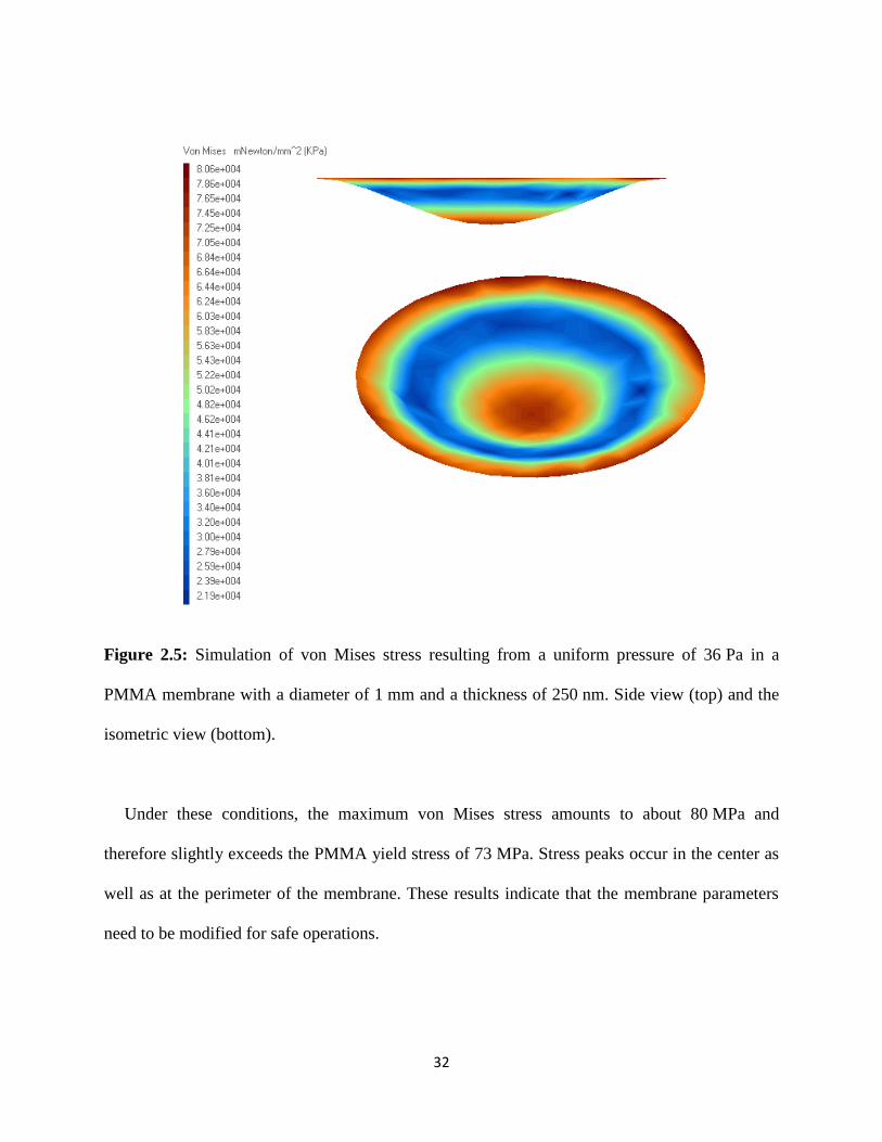
32
Figure 2.5: Simulation of von Mises stress resulting from a uniform pressure of 36 Pa in a
PMMA membrane with a diameter of 1 mm and a thickness of 250 nm. Side view (top) and the
isometric view (bottom).
Under these conditions, the maximum von Mises stress amounts to about 80 MPa and
therefore slightly exceeds the PMMA yield stress of 73 MPa. Stress peaks occur in the center as
well as at the perimeter of the membrane. These results indicate that the membrane parameters
need to be modified for safe operations.

33
2.2. Surface Energy Density Model applied for Post Processing of the Pore to fine tune the
Diameter
According to chapter 1.5, electron beam lithography was selected for patterning the
membrane. Lower acceleration voltage machines accessible within this research are not
necessarily capable of patterning pores down to a few dozen nanometers in diameter in
membranes of at least several hundred nanometers thickness. In the context of the research goal,
being able to fabricate pores with variable sizes, a two-step nanopatterning sequence can be
pursued: The first step comprises lithographic patterning of the smallest pore possible, and on the
second step augments the result applying additional postprocessing techniques. These could
involve adding a coating to the pore walls, or reshaping the pore in a reflow process.
The latter is the approach taken since thermoplastic membranes fundamentally allow for
reshaping. UV exposure can be applied to reduce the pore diameter by minimizing the surface
energy of the solid. This approach is based on a model by Storm et al. [32]: At high
temperatures, many solids start to deform. For instance, when exposed to high-energy beams
and, thus high temperatures, membranes have a tendency to deform and lower their surface free
energy by changing their surface area. In membranes containing a pore, changes in surface area
will cause the pore to either shrink or expand in diameter, while the pore volume remains
constant. In Storm’s original model, electron beams are applied. We do not have the appropriate
instruments available for experiments, and use broadband UV light as the energetic radiation
instead. This approach has additional benefits as pertaining to the control of surface charges on
the PMMA membrane, which will be discussed in later chapters.
Since pores can either expand or contract upon exposure, Storm’s model will be briefly
discussed in terms of a single-pore layout [53]: A membrane with a single cylindrical pore of

34
radius r and constant length L is kept under constant uniaxial tension P’ and at a high
temperature. The pore has an overall surface A, consisting of the actual pore walls as well as the
imaginary top and bottom lids. With the surface energy density of the membrane γ, the variation
of total Gibbs free energy at equilibrium G is given by
(2.3)
This change in free energy therefore delivers
(2.4)
in which the overall pore surface A described above is given as
and
(2.5)
The surface energy density γ can then be written as:
(2.6)
This delivers geometrical constraints for a membrane with a pore, lowering its surface free
energy when exposed to high-energy beams: The membrane will reduce the pore radius r if the
pore has an original radius r < L/2. However, it will increase the pore radius if the pore has an
original radius r > L/2 [32, 53]. In other words, only selected pores will laterally shrink upon this

35
kind of post processing: the original pore needs to be at least twice as long (deep) when
compared to its radius. In terms of aspect ratio, which is the feature height divided by the
minimum lateral feature size, the length-to-diameter ratio must exhibit an aspect ratio of at least
one.
Due to the geometrical constraints in this research, aspect ratios larger than one are applied,
and a reflow post processing sequence can therefore theoretically be applied to optimize the
diameter.
2.3. Theoretical Model for the Electrophoretical Derivation of Pore Dimensions
The performance of the electrophoretic detector system will primarily be determined by the
actual dimensions of the pore. These dimensions can get established via metrology techniques,
but many of them do not provide sufficiently precise data or do not necessarily deliver the
diameter at the minimum cross section. An alternative is to use the detector properties
themselves to derive the dimensions electrochemically, using the ionic resistance/conductance of
the pore as follows [49, 45, 50]:
Geometrical parameters are evaluated by measuring the ionic resistance of the device under
its intended operation. Subsequently, the results are referenced to each other and to simulated
data. Assuming ohmic conductance, the open pore current Iopen through a pore can be correlated
to the pore diameter D and length L by
(2.7)
where K’ is a constant dependent upon the voltage and electrolyte resistance [48]. An
approximations for the resistance of a pore can be obtained as [51]

36
(2.8)
where A(L) is the pore cross sectional area perpendicular to its length L, and K is the specific
conductivity of the electrolyte inside the pore.
Integration of equation 2.8 under the restriction of cylindrical pore shapes, which can be
approximated by small pore diameters D compared to their length, or high aspect ratios as
already stipulated in the preceding chapter (L>>D), delivers [52]
(2.9)
which can be solved for the pore diameter D as
(2.10)
The unknowns in this equation can exactly be obtained: The pore length L corresponds to the
membrane thickness and is determined by stylus profilometry or similar techniques. V is the
voltage applied across the membrane, and I is the current through the pore. Both electrical
parameters V and I are well controlled using a high precision patch clamp test setup. The
electrolyte conductivity K determines the resistance of the pore itself and is measured by the
steady-state ionic current flowing through the pore at a given applied external voltage.

37
The pore diameter D derived from equation 2.10 is an exact solution for cylindrical pores. For
symmetric pores, it can serve as an approximation of the effective diameter. For all pores of
similar cross section, it is a powerful tool to compare pore diameters relative to each other.
2.4. Deblois Resistance Variance Model for Analytical Predictions of Electrophoretic
Current Blockades
Developing a model to theoretically predict the electrophoretical performance of a pore has
many benefits: Results can be implemented in the design of the required geometry. They can also
be used to compare theoretical and experimental results in order to better understand
experimental results or to discriminate between measured translocation effects and artefacts. The
model can be verified by comparing predicted and measured data when analyzing translocations
of known particles through the pore.
Translocation events are often associated with an increase in resistance ∆R due to the
presence of nanoparticles inside the pore. This additional resistance leads to a temporarily
reduced current or current blockade Iblock, which is also denoted as ∆I in some of the formulas. A
variety of models have been proposed in literature to estimate the resistance variance exerted by
a single particle translocating through a pore. None of them, however, are proven valid for all
kinds of pores in terms of various shapes and dimensions. In other words, there is not yet an
exact single model described in literature by which translocation events of single particles
passing through all different kinds of pores could be evaluated. For example, Maxwellian theory
employs an ingenious argument, by which a simple model was obtained using the effective
resistivity ρeff of a diluted suspension of insulating spheres in a solution of original resistivity ρ’.
The effective resistivity is a function of the volume fraction of the spheres in suspension [51].
The Maxwellian expression of resistance variance can be used either to size the particles or to

38
measure the pore diameter. However, although the expression is correct for a small sphere in
comparison to the pore diameter, it estimates lower ∆R values than the actual experimentally
measured ones. This is because the model considers the total current with uniform distribution
inside the pore [51].
Another approach to look at the resistance variance induced by a translocating particle is to
consider a translocating sphere in a uniform electric field instead of investigating the current
[52]. Deblois proved that this assumption can generate a model that is valid over a broad range of
pores with different shapes and dimensions. In this model, the applied constant potential
difference across the pore creates tubular current streamlines that slightly bulge around the
translocating sphere. Compared to other previously proposed models, these assumptions and
descriptions seem to be closer to what really occurs in a pore with a translocating particle. This
model gives rise to higher values of resistance increase induced by a translocating particle
compared to the Maxwellian model [54]. Figure 2.6 represents the cross section of a pore with
diameter Dm and length L. The broken lines symbolize two electric field lines with a separation
of D(z) varying along the axis z along the pore. Inserting a non-conducting sphere of diameter d
modifies the originally uniform field and leads to bulging of the field lines. The pore walls at Dm
limit the maximum bulge the field lines can experience [55].

39
Figure 2.6: Schematic of the cross section of a pore with a non-conducting sphere and electric
field lines [55].
To satisfy the spherical boundary conditions, Deblois proposed a solution of Laplace’s
equation of the first odd zonal harmonics, i.e.
(2.11)
V is the applied potential. r is the distance and θ is the angle measured from the z-axis, as
illustrated in Figure 2.6. A and B are constants and will be determined based on the boundary
condition at the sphere surface that changes in the field normal to the insulating sphere surface
must be zero:
and (2.12)
40
Inserting equation (2.12) into equation (2.11) delivers
(2.13)
This potential describes tubular current field lines that slightly bulge around the sphere as
shown in Figure 2.6. It is an exact solution for such a bulge shape inside the pore. Experimental
verification by Deblois further showed that the bulge shape size depends on the proportionality
between the sphere diameter d and the pore diameter Dm. The bigger the sphere, the bigger is the
bulge size. If d/Dm=0.5, for instance, the bulge size is only 7% [52].
Based on this bulged field, the variation in pore resistance R can be approximated by
comparing the resistance in the center of the bulge R2 to a situation in the absence of a particle at
all, the unobstructed case with open pore resistance R1. R1 therefore constitutes a lower limit of
the pore resistance and the distribution of the total current can be assumed uniform across the
cross section in this case.
Integration of the electric field from the center line to the pore walls will deliver the potential
difference. Using the electrolyte’s resistivity ρ’, Ohm’s law translates this into the total current
along the z axis through any cross section with diameter D and distance z from center of sphere
as
(2.14)
where x is the distance from the central axis, and Ez is the component of the electric field along
the z axis. Ez can be written as

41
(2.15)
The lower limit of the integration in equation 2.14 can vary between zero and d/2. The first
case represents the pore center line as the integration limit, in areas where there is no sphere,
corresponding to |z| values larger than d/2. The second case puts the integration limit right to the
full radius of the sphere, corresponding to a |z| value of zero. Equation 2.14 therefore turns into
(2.16)
as a general case. When z = 0 at the bulge, the equation simplifies into
(2.17)
Continuity demands that a given current through the pore is constant along the pore, no
matter whether a region with the sphere |z| < d/2 is considered, or an area beyond the sphere
|z| > d/2. Equating equations 2.16 and 2.17 therefore results in an implicit expression for D(z)
(2.18)

42
Ohm’s law, using equations (2.13) and (2.17), deliver the pore resistance in the presence of a
sphere R2
(2.19)
The resistance variance is limited by the lowest resistance R1 in the completely unobstructed
case. This case is much easier to derive and is based on the most useful approximations for the
resistance of a tube of varying cross section (equation 2.8). This leads to an approximation for R1
(2.20)
Since the physical size of the pore does not change, and since the field lines resemble
streamlines continuously linking the areas without and with a sphere, the expression developed
for D in equation 2.18 can be substituted for D2 in equation 2.20, delivering R1 as
(2.21)
Equations 2.19 and 2.21 determine the resistance variance R as
(2.22)

43
This equation constitutes an upper limit of the resistance variation if D is substituted from
equation 2.18. When d « Dm, D=Dm is a valid approximation, and equation 2.22 can be
integrated as [52]
(2.23)
This model has preserved the Maxwellian value as its limit and seems to be the most
appropriate for the pore diameter of 454 nm in [52] where the sphere size is smaller than the pore
size. In this model, ΔR also shows a high independency of the pore length, which means it can
determine Dm quite locally. The expression for the variation in resistance ΔR derived in
equation 2.23 can be simplified using series expansion, which delivers the following
approximation:
(2.24)
Using this model, the magnitudes of the current blockage spikes Iblock = I can be determined
as follows [54]
(2.25)

44
where Iopen represents open pore current, Ropen is the pore resistance in the absence of particles,
previously introduced as R1, and ∆I is the current blockade Iblock.

45
3. Design of an All-PMMA Electrophoretic Flow Detector
As discussed in chapter 1, single synthetic micro-/nano-meter-sized pores embedded in an
insulating membrane are the basis for a promising class of detectors for rapid electrical detection
and characterization of biomolecules. Like their biological counterparts, these detectors can
quantify and eventually identify biomolecules based on the conductance of current through the
pores [56]. Fabrication of synthetic micro- or nanopores offers several obvious advantages over
biological nanopores. These include flexibility in pore diameter and length; high stability against
external parameter variations such as the pH value of the solutions, salt concentration,
temperature, and mechanical stress; adjustable surface properties of the pore; as well as
integration possibilities into devices and arrays [18, 57].
To fabricate such an electrophoretic flow detector, fundamental design considerations need to
be made before proceeding to the microfabrication stage. These considerations include the
selection of the membrane material and the definition of the geometry of the membrane and the
pore itself.
3.1. Material Selection
3.1.1. Membrane
The selection of the membrane material requires precise consideration of its mechanical,
electrical, physiochemical, and biological properties in order to provide optimal performance,
both from a manufacturing and an operational point of view. Some of the characteristics that
determine the suitability of a material as a membrane for the detector, such as polyimide (PI),
polystyrene (PS), polycarbonate (PC), polyethylene terephthalate (PET), or
polymethylmethacrylate (PMMA), are listed below [58, 59, 35]:

46
Mechanical Strength and Stability – The membrane material needs to be able to withstand
the typical forces that are generated during fabrication (e.g. thermal stress or point forces)
and operation (e.g. differential pressure caused by the electrolyte). It should also be able to
flexibly deform rather than rupture.
Membrane Durability and Lifetime - The material needs to allow for a long device lifetime
in order to be used in long-term experiments and be re-used for multiple experiments and
analyses.
Optical Transparency - Several microfabrication steps, such as alignment for systems
integration, and many aspects of operations, such as filling the reservoirs with electrolyte,
are facilitated significantly if the detector system is optically transparent. This allows for
inspection under a microscope or for working with the device under a stereo microscope.
In some cases, fine-tuning processes of the micro/nanopore are based on optical
approaches. These require the chosen membrane material to be transparent.
Biocompatibility -Biocompatibility is a vital issue to any medical and biomedical device or
implant. It describes the suitability of a material for exposure to the body or bodily fluids.
In the case of implants, a material will be considered biocompatible, if it allows the body to
function without any complications such as allergic reactions or other adverse effects. In
the case of biomedical detector systems, none of the biomolecules to be detected may be
altered, degenerated, or even only change their conformation upon contact with the
material, or else the measurements would be falsified. Biocompatibility requirements
reduce the choice of membrane materials significantly.
Chemical Resistivity - Chemical resistivity is required to ensure that the membrane does
not alter in its intended operation. The environment is potentially aggressive including the

47
electrolyte solution or body fluids, and many materials could temporarily take up some
water and swell, or permanently dissolve, causing loss of structure accuracy or even
structure collapse.
Hydrophilicity – From Greek ‘loving water’, or attracting water, such that the device can
be wetted. This is a key requirement specific to the electrophoretic detector application and
has proven to be one of the hardest conditions to meet in past studies: With decreasing pore
sizes, it is increasingly difficult to ensure that the pore is at all, and entirely, filled with
electrolyte, which would be the precondition for electrophoretic measurements. To support
wetting of the membrane and its pore, the chosen material must be sufficiently hydrophilic.
Good membrane hydrophilicity not only fundamentally allows any measurements, but also
supports transport of the expected molecules through the pore, and helps to prevent their
adherence or absorption onto its surface and pore wall.
Process Compatibility - Manufacturing of a detector device entails a lengthy process chain,
consisting of patterning, cleaning, and systems integration steps. Lithographic
microfabrication of micro/nanopore in the membrane material, for instance, includes the
exposure to energetic radiation and wet chemical development, the application of chemical
rinsing and stripping agents, the exposure to elevated temperature, and possibly various
postprocessing sequences. Systems integration exposes the membrane to glues and
etchants. The membrane must withstand all of these in order to support the pore and
warrant its fabrication with high geometrical accuracy and reproducibility.
Compatibility with optional Surface Modification Techniques - After fabrication of the
micro/nanopore, the membrane might be exposed to chemical modifications or chemical
enhancement of its surface to increase its hydrophilicity/wettability or to introduce an

48
immobile phase. Another goal of surface modification might be to covalently attach
different bioactive compounds which catalyze or elicit a specific response within a given
biological system, for instance to capture elements such as antibodies. Therefore, stable
and diverse modification of surface chemistry must be supported by the membrane
material.
Thermal Properties - To minimize thermal defects caused during the fabrication process,
the material needs to possess good thermal properties, such as a high glass transition
temperature Tg or a comparatively high thermal conductivity.
Electrical properties - To minimize dielectric-breakdown effects when operating at modest
to high electric field strengths, the membrane material needs to possess good electrical
insulating properties.
Surface Charge Density - The surface of a chosen membrane material needs to be
homogenous in terms of the density of the charge that it is carrying; surface heterogeneity
observed in some materials creates spots with non-uniform surface charge densities on the
dielectric membrane, causing localized changes in the ionic current through the pore,
affecting the electrophoretic efficiency.
Ionic Current Carrying Capability - The membrane material needs to support the passage
of a steady and stable ionic current through the pore, in order for the pore to be able to
reliably detect the changes in the ionic current that are caused by the translocation of
molecules through the pore. The surface charge of the membrane might be changed during
the fabrication process, such as a UV-exposure for reflow-based post processing, or even
during the operation of the detector system, depending on the pH value of the electrolyte
solution. It must be possible to neutralize these charges on the membrane either

49
permanently using processes compatible with the material, or temporarily, to warrant the
passage of a steady and stable ionic current through the pore [31, 38, 50, 60].
Polymer materials are promising candidates to meet most of the requirements mentioned
above. Polymethylmathacrylate in particular has the additional advantage that it can be
excellently micro- and nanopatterned. In the present research, PMMA is therefore applied as the
membrane material for the fabrication of micro/nanopores forming part of an electrophoretic
flow detector. In more detail, this selection is due to the following material properties:
PMMA can directly be patterned as the structural material. Other materials often just serve as
a processing mask for subsequent etching, or get etched by themselves using a different
processing mask. This eliminates the need for an etching step and therefore increases the
potential structure accuracy and reduces potential minimum feature sizes. PMMA is compatible
with different lithographic techniques, and has a proven and outstanding track record of high
resolution patterning by electron beam lithography (EBL) and X-ray lithography (XRL) [42]. It
is a transparent thermoplast, allowing for an optical feedback during fabrication (alignment
steps) and operation (filling of reservoirs, electrode positioning, etc.). This is a benefit almost
exclusive to PMMA, when compared to other competing materials. PMMA can not only be
micro/nanopatterned, but it is also rigid and ductile enough to get machined. This allows for an
almost unique opportunity to fabricate not only the membrane, but also all supporting
components of PMMA. On a systems concept level, this enables integration in to the detector
structure made of the same material (single-material integration). PMMA is rated excellent for its
biocompatibility, several commercial grades (e.g. Plexiglas®) are even officially assigned US
Pharmacopeia (USP) Class VI biocompatibility. It has therefore been used in many biomedical
applications and microchip electrophoretic systems [31]. Its comparatively high hydrophilicity

50
(contact angle with de-ionized water was reported to be between 71.7° ± 1.5 and 73.7° ± 1 for
comparable PMMA grades) supports wetting properties in the micro-fluidic domain [43].
PMMA, like many other micro-patterned polymers, tends to build up a negative surface charge
during fabrication process, likely to a larger extent than observed in silicon-based materials. This
could be disadvantageous for its intended uses. The charge build-up in PMMA can be alleviated,
however, by a variety of different surface modification techniques, such as wet chemical
methods, X-ray and UV-irradiation, and oxygen or air plasma treatment. The available surface
modification techniques are able to not only neutralize the negative surface charges created on
the PMMA membrane, but to also make the PMMA surface even more hydrophilic. These
methods, however, can cause material damage and compromise the thermo-mechanical
properties.
These properties made PMMA the preferred membrane material in this research. The
monomer methyl meth acrylate has a molar mass of about 100 g/mol and a molecular structure as
shown in Figure 3.1.
Figure 3.1: Molecular structure of methyl methacrylate, the monomer of PMMA.
Polymerization of these monomer units forms PMMA. PMMA can consist of up to tens of
thousands of monomer units per macro molecule, with typical molecular weights Mw around
1 million g/mol. Table 3.1 highlights its advantages and disadvantages when compared to

51
competing, already published, non-polymer pore-based detector approaches. The competitors in
the list are artificial pores in a silicon membrane, and natural protein pores in a lipid bi-layer.
Trends highlighted in the table are based on a literature search [18, 33, 42].
Table 3.1: Summary of important flow detector properties based on different membrane
materials, taking into account typical fabrication approaches.
Characteristics PMMA-Based Silicon-Based Protein Pore-
Based
Nano-patterning
of membrane
Direct
lithography
Etching
Self assembly
Single-Material
Integration
Yes Not usually No
Optical Transparency Yes No No
Pore Size
Range/Tunability
Wide Wide None
Minimum Pore Size Nanometers Nanometers Nanometers
Lifetime Months/multi-usage
demonstrated
Not reported Hours/single use
Known Drawbacks • Minimum pore
size demonstrated
• Surface charging
• Wettability
• Noise levels
• Reproducibility
• Tolerable
environment
(e.g. temp., pH)
Sensitivity of Pore
Surface Properties to
Processing
Conditions
High Low
(can be increased by
Self-Assembled
Monolayers)
Low
(can be increased by
enzymes/proteins)
3.1.2. Detector System
While the membrane is the key component in the detector device, it is only one component in
a larger system. The system needs to provide electrolyte compartments and an adequate support
for the membrane as well as structures for assembly. The system also needs to provide a
hermetic seal between the various components to avoid fluidic leakage. This is best ensured by
minimizing the potential amount of thermal stress due to thermal expansion coefficient
mismatches of different materials. Therefore, a single-material approach which uses the same

52
material with identical properties for all system components is desirable. Consequently, PMMA
is chosen for all auxiliary components as well.
3.2. Geometry of the micropatterned Membrane
The dimensions of the membrane, the dimensions and the shape of the micro/nanopore itself,
and the dimensions of the auxiliary components must be determined. They will all affect the
overall performance of electrophoretic detector device, including its accuracy of detection and
the quality of analyses of particles and molecules. In a first step, the membrane dimensions will
be determined, ignoring the pore itself. As discussed in chapter 2, 2-dimensional finite element
methods (2D FEM) are an appropriate tool to analyze the mechanical behaviour under different
load cases for possible geometries. Results will be evaluated to determine best dimensional
characteristics of the whole detector device.
3.2.1. Membrane Dimensions
As discussed in chapters 1.5 and 2.1, the membrane diameter D and the membrane
thickness L have a strong impact on the patterning process and the structure quality of the pore as
well as on mechanical stability, integration tolerances, and on the electrophoretic performance of
the device. These aspects impose opposing requirements on D and L:
- A thinner membrane alleviates the micro-/nano-patterning processes, and the patterned
pore can be wetted more easily. It will also result in an increased open pore current Iopen
under otherwise similar conditions, and therefore allows for a highersignal to noise ratio.
But a thin membrane is more susceptible to failing under mechanical stress during
fabrication and operation.

53
- A larger membrane diameter allows for less precise alignment during systems
integration, which might enable manual processing without the need for additional
equipment or active feedback. Larger membranes, however, are again more vulnerable to
mechanical stress.
Therefore, a compromise between sufficient stability (thick, small membrane) and alleviated
processing (thin, large membrane) as well as device performance needs to be determined.
PMMA membrane thickness and diameter are therefore numerically studied. For different
geometrical setups, the von Mises stress is simulated as explained in chapter 2.1 as a model for
the equivalent stress in a three-dimensional load case. Figure 3.2 illustrates a typical simulation
result for a membrane in its critical situation. The load case is based on the geodetic pressure of
only one entirely filled electrolyte reservoir, which is a typical temporary situation during filling
the detector. The water pressure head can amount to a maximum of 3.68 mm (compare
chapter 2.1), corresponding to a pressure of 36 Pa. For a membrane with 1 mm diameter, a
thickness of at least 265 nm is required. In this case, the membrane would just barely survive the
load, but no safety margins are available: The maximum von Mises stress is about 72 MPa,
which is very close to the yield stress of 73 MPa taken from ISO 527. The yield stress is the
material property associated with the load under which the PMMA membrane will start to
rupture.

54
Figure 3.2: Simulated von Mises stress for a PMMA membrane with 1 mm diameter and
265 nm thickness under a pressure of 36 Pa.
Geometrical parameters are subsequently varied to find an optimum combination of thickness
and diameter. Figure 3.3 illustrates how the maximum von Mises stress increases with
decreasing membrane thickness and increasing membrane diameter respectively. The load case
of an assumed electrolyte level of 3.68 mm is kept constant. At a fixed diameter of 1 mm, a
membrane thickness of at least 265 nm is required, which is the specific case illustrated above.
At a fixed thickness of 1000 nm, the maximum diameter is close to 4 mm. Further decreasing the
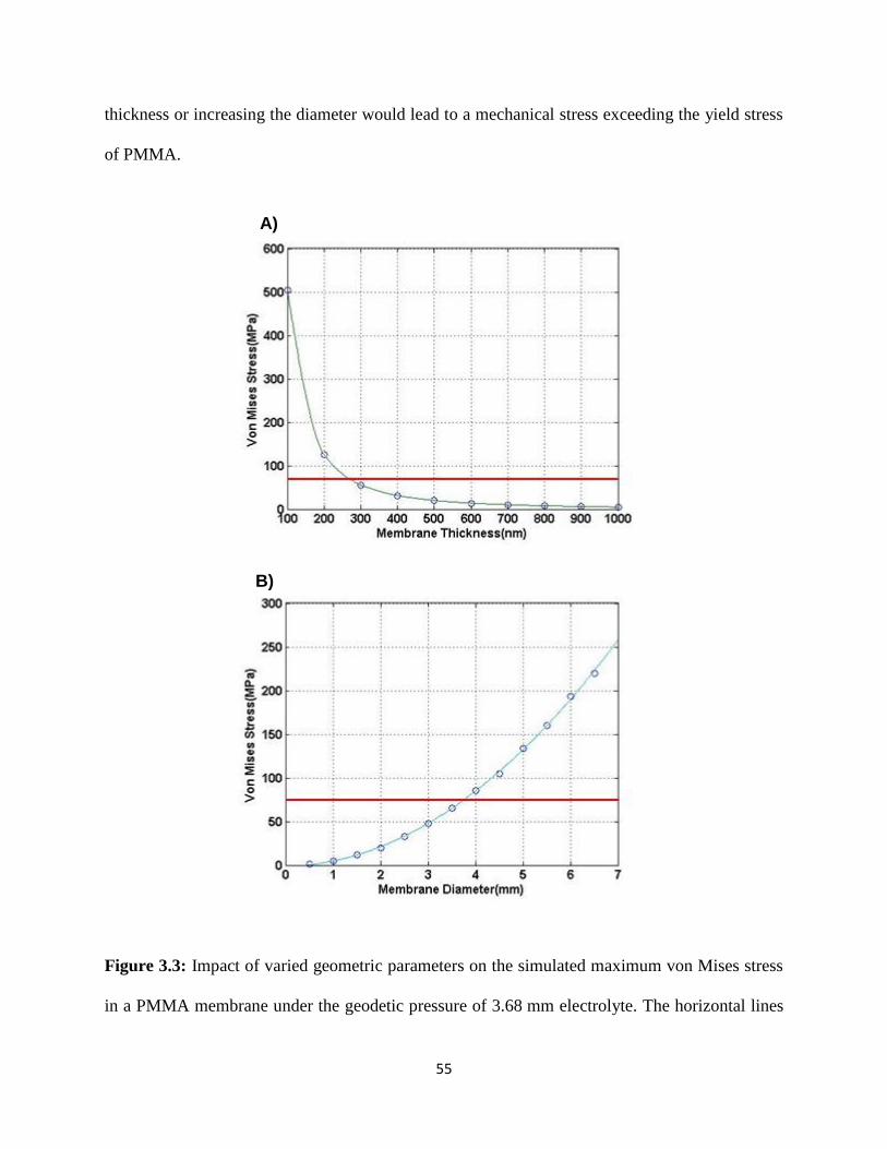
55
thickness or increasing the diameter would lead to a mechanical stress exceeding the yield stress
of PMMA.
Figure 3.3: Impact of varied geometric parameters on the simulated maximum von Mises stress
in a PMMA membrane under the geodetic pressure of 3.68 mm electrolyte. The horizontal lines
B)
A)

56
represent the materials properties-related limit for the acceptable stress (yield stress of 73 MPa):
(A) Variation of the membrane thickness between 100 nm and 1000 nm at a fixed diameter of
1 mm; (B) Variation of the membrane diameter between 0.5 mm and 6.5 mm at a fixed thickness
of 1000 nm.
The simulated geodetic pressure is only one of several contributions of stress on the
membrane. Others include expected stress peaks during fabrication, such as during the
membrane release step. A safety margin is therefore added to the simulated minimum membrane
thickness of 265 nm at 1 mm diameter. This is anticipated to increase the fabrication process
yield significantly, while compromising on the electrophoretic performance. A membrane
thickness of 1 µm was considered to be a good compromise. In later experiments, such a
membrane in fact never ruptured during operations, but a few did rupture during fabrication.
Figure 3.4 shows the simulated stress distribution for the load case of 36 Pa geodetic pressure
which formed the basis of the previous simulations as well. The maximum equivalent stress of
about 50 MPa remains well below the yield stress of 73 MPa.

57
Figure 3.4: Simulated distribution of von Mises stress in an unpatterned PMMA membrane with
1 mm diameter and 1 μm thickness under a pressure of 36 Pa. Side view (top) and isometric view
(bottom).
The membrane will slightly deform as a result of the differential pressure. The simulated
stress translates into a maximum displacement of the center of the membrane of about 0.1 mm as
illustrated in Figure 3.5. The graphical representation of the deformation is not to scale. During

58
actual operations, the displacement will be reduced as soon as electrolyte is filled into the second
reservoir and the pressure gets compensated to a large extent.
Figure 3.5: Simulated membrane displacement in a PMMA membrane with 1 mm diameter and
1 μm thickness under 36 Pa pressure. Side view (top) and isometric view (bottom), not to scale.
3.2.2. Pore Dimensions and Shape
As discussed in chapter 2, length and diameter of the pore are the important geometrical
properties that will affect the detector device performance.
The pore length L is given by the membrane thickness T and has just been defined to be 1 µm
in the previous FEM analysis section. The pore length not only affects the device stability, but

59
also its performance. According to the equation 2.6, a pore with a shorter length will provide a
larger open pore current Iopen at otherwise constant conditions. Since typical currents are on the
picoampere scale, larger currents, corresponding to shorter pores or thinner membranes, are
desirable for the measurements.
The pore diameter d can still be freely determined within the boundaries dictated by
fabrication capabilities. A larger pore diameter will result in a larger open pore current Iopen. A
larger open pore current will have smaller relative fluctuations at otherwise similar conditions, or
a better open pore signal-to-noise ratio. At the same time will particles of a given size create
smaller relative temporal current blockades if the pore and open pore current are larger. If the
pore diameter is too big compared to the diameter of particles/biomolecules to be detected, the
large open pore current will only slightly change upon translocation, which impedes reliable
detection. Eventually, some translocations might not get detected at all, which results in an
underestimation of the frequency of translocations and therefore the particle concentration in the
electrolyte [61]. Since current blockades constitute the key measurement signal, the primary goal
is to maximize the signal change upon translocation of a particle to be measured. In other words,
the diameter of pores in an electrophoretic biomedical detector should always be slightly larger,
but comparable to the size of the biomolecule or pathogen to be detected. This facilitates
monitoring and analysis of the obtained changes in Iopen upon translocations through the pore [9]
avoids underestimating the frequency of translocation events [61].
These considerations determine reasonable upper and lower limits of the pore diameter,
depending on the size of particles to be analyzed. Particles, biomolecules, and pathogens of
interest cover a wide range of sizes from a few nanometers up to several hundred nanometers.
The largest pores to be fabricated are thus designed to have 1 μm in diameter. The smallest size

60
desirable would be a few nanometers and for our initial tests in reality is determined by the
smallest feature that still has a reasonable process yield in 1 μm thick PMMA. We decided to
plan for minimum feature size of 200 nm in a first detector layout. Pore post processing might be
applied to further shrink that size.
The third important geometrical property of the pore, besides its dimensions given by length
and diameter, is its detailed shape. Aspects of the pore shape cover its lateral shape in the plane
of the membrane, and the shape across the membrane, along the pore. Analyzed particles of
interest do span a wide range of diameter-to-length ratios, but are considered to be more or less
rotation symmetrical. We therefore design our pores to be circular openings in the lateral plane
of the membrane as well. The exact cross section across the membrane requires some more
consideration. The pore width can be constant along the pore, which would correspond to a
cylindrical pore. If the cross section gets narrowed or wider along the pore, i.e. across the
membrane, the pore is conical. Naturally occurring protein pores sometimes feature even more
complicated geometries as illustrated in Figure 1.6. This cross-sectional shape of the pore can
affect the overall performance of the detector: Conical pores with an increased diameter at the
front, or inlet, of the pore, for instance, may help to guide and orient molecules in the vicinity
into the narrower constriction of the pore [14]. Therefore, conical apertures with such an
orientation are anticipated to increase the frequency of translocation events of molecules through
the pores, which could be advantages for samples with very low particles concentration in the
electrolyte. Furthermore, conical pores are attributed to possess a reduced effective length
compared to cylindrical pores. However, conically-shaped pores are extremely difficult to
fabricate in a controlled and reproducible manner. We will, therefore, focus on microfabrication
of cylindrical pores in 1 μm thick PMMA membranes.

61
3.2.3. Auxiliary Components of the Detector Device
To act as an electrophoretic detector, the patterned membrane needs to be supported and
integrated into two chemically and mechanically stable reservoirs for the electrolyte solution,
access paths for electrodes have to be provided, and a save stand must be added. A layout with a
vertical orientation of the membrane will allow to minimize the differential pressure on the
membrane. If the entire system is planned symmetrically, no additional considerations, e.g. with
respect to the exact positions of the electrodes, are necessary. All components will be made of
PMMA to follow the single-material approach discussed earlier.
Following these design considerations, the following auxiliary device components are laid
out:
two electrolyte reservoirs with openings at the top to fill in the electrolyte and to add the
electrodes
two rings to support the patterned membrane from either side
two stands for the detector system
Figure 3.6 shows an explosion graph of these auxiliary components. The patterned membrane
would be added right in the center. The alignment grooves in the support rings will be explained
in detail further down and in the fabrication section in chapter 4.

62
Figure 3.6: Explosion graph of the auxiliary detector components.
Details, including all dimensions, can be taken from Figure 3.7. Numbers are dimensions in
millimeters. Section A-A, for instance, defines the overall system length to be 33.6 mm.
The electrolyte reservoirs are filled using the injection and drain inlets at the top. These inlets
also allow to position two electrodes in the vicinity of either side of the membrane for the
electrophoretic measurements. The reservoir dimensions are designed so that the head pressure
cannot exceed the 3.68 mm limit defined in the FEM analyses. View B in Figure 3.7 illustrates
how the geodetic pressure increases from top to bottom of the reservoir, assuming complete and
one-sided filling. The maximum pressure 3.68 mm from the top, 36 Pa, was used as a constant
pressure in the simulations previously discussed to cover a worst-case scenario. Since pressure is
a scalar quantity, it is independent of direction, and the membrane orientation therefore has no
impact under this worst-case assumption.
View A: PMMA disc in Figure 3.7 represents a support ring which will be mounted to the
membrane to prevent the membrane from rolling up. The ring has a diameter of 13 mm and a
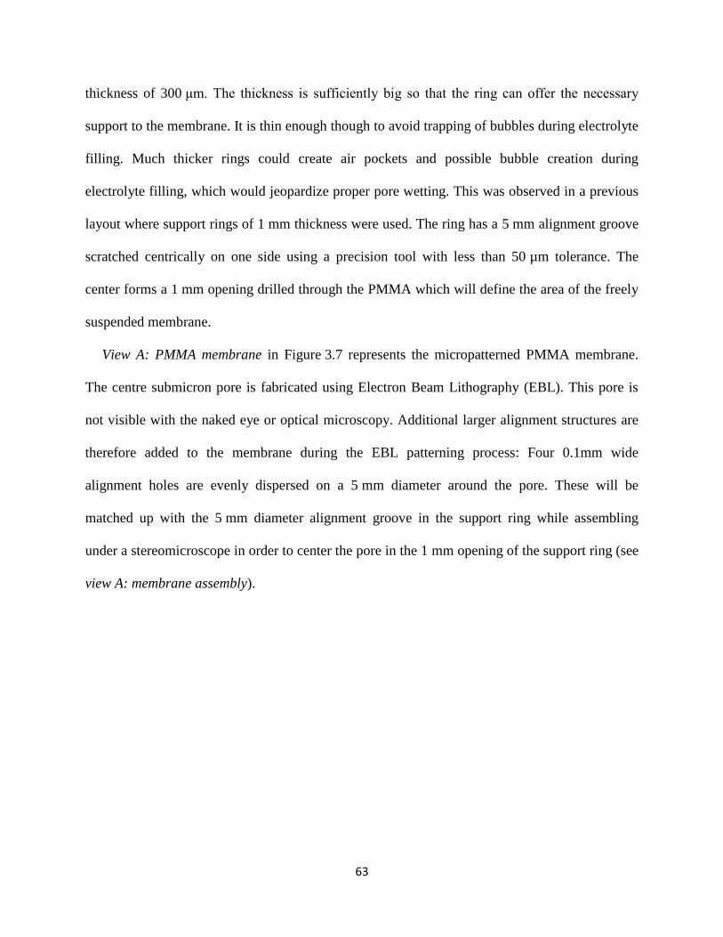
63
thickness of 300 μm. The thickness is sufficiently big so that the ring can offer the necessary
support to the membrane. It is thin enough though to avoid trapping of bubbles during electrolyte
filling. Much thicker rings could create air pockets and possible bubble creation during
electrolyte filling, which would jeopardize proper pore wetting. This was observed in a previous
layout where support rings of 1 mm thickness were used. The ring has a 5 mm alignment groove
scratched centrically on one side using a precision tool with less than 50 µm tolerance. The
center forms a 1 mm opening drilled through the PMMA which will define the area of the freely
suspended membrane.
View A: PMMA membrane in Figure 3.7 represents the micropatterned PMMA membrane.
The centre submicron pore is fabricated using Electron Beam Lithography (EBL). This pore is
not visible with the naked eye or optical microscopy. Additional larger alignment structures are
therefore added to the membrane during the EBL patterning process: Four 0.1mm wide
alignment holes are evenly dispersed on a 5 mm diameter around the pore. These will be
matched up with the 5 mm diameter alignment groove in the support ring while assembling
under a stereomicroscope in order to center the pore in the 1 mm opening of the support ring (see
view A: membrane assembly).

64
Figure 3.7: Overview and dimensions of the all-PMMA detector system components.
After appropriate materials were identified and all functional and auxiliary shapes and
dimensions determined in this design chapter, the fabrication sequence will be discussed in the
upcoming chapter.

65
4. Fabrication Procedure and Detector Integration
Based on the design considerations detailed in the preceding chapter, chapter 4 now focuses
on developing and improving the fabrication processes for all individual components of detector
devices. These include the fabrication and submicrometer patterning of the membrane using
electron beam lithography (EBL), optional post processing of the pore to further reduce the
diameter, mechanical microfabrication of the auxiliary PMMA components, and finally
membrane release, alignment, and hermetic sealing of the components in a systems integration
sequence.
4.1. Pore Fabrication by Electron Beam Lithography
The membrane is fabricated on a silicon wafer as a sacrificial substrate. The first step in the
fabrication sequence comprises cleaning of the substrate with acetone to remove potential debris
from the wafer surface. PMMA is then spin-coated to form a 1 μm thick film. Parameters are
2500 rpm for 45 seconds using PMMA 950 A8 by MicroCHEM. It is a PMMA grade with a
molecular weight of MW = 950,000 g/mol with a solid content of 8%, dissolved in anisole.
Subsequent baking in a convection oven is done at 170°C for 30 minutes.
The third step is micro- or nanopatterning the film. This step is the key to the future device
performance as it determines, to a large extent, the structure quality and accuracy of the pore. As
discussed in chapter 1.5, electron beam lithography (EBL) is applied in this research. PMMA is
particularly well suited for patterning by EBL as it is one of the highest contrast, standard resists.
Feature sizes down to a few nanometers can get fabricated using optimized process conditions.
The fabrication challenge is to produce small pores in comparatively very thick resist. The aspect
ratio, defined as the ratio of resist thickness to minimum lateral feature size, does not usually

66
exceed 2 or 3. Pores with diameters smaller than 500 nm in the 1 µm thick PMMA film will
therefore need significant process optimization. Furthermore, scattering effects of incident
electrons widen the electron beam in the resist resulting in non-vertical walls and poor structure
quality. Cylindrical pore can only be fabricated at high initial electron energies, i.e. high
acceleration voltages, and on a substrate with minimum back-scattering.
The penetration depth of electrons has been empirically determined by Schonland [62] as
(4.1)
where Dp is the penetration depth, K” is an empirical coefficient equal to 2.1, ρ is the density of
the exposed material, and V is the accelerating voltage. Figure 4.1 plots this formula of the
electron penetration depth in PMMA as a function of the accelerating voltage. To even allow
electrons to propagate 1 µm into the PMMA, an acceleration voltage of at least 8 kV is needed.
Higher voltages will improve the structure quality achievable. The highest acceleration voltage
available in reasonable distance to our laboratory is a Raith 150 EBL electron beam writer with
up to 30 kV acceleration voltage, located at the University of Alberta NanoFab in Edmonton. It
is represented by the vertical line on the left in Figure 4.1 Higher acceleration voltage writers are
fabricated, for instance, by Elionix, Tokyo, Japan, who have demonstrated 15 nm wide lines in
1.5 µm thick resist with a 120 kV machine (represented by the vertical line on the right in
Figure 4.1).
In this study, we use 30 kV with an exposure dose finally set to 315 μC/cm2 to transfer the
pattern. Future tests should be made using dedicated beam writers with increased acceleration

67
voltage. A 50 kV writer (Jeol JBX-6000) would be available in eastern Canada at the National
Research Council Institute for Microstructural Sciences, for instance.
Figure 4.1: Electron penetration depth in PMMA as a function of the accelerating voltage.
Acceleration voltages of 30 kV used in this study (Raith) and 120 kV as an example of a high
voltage writer (Elionix) are highlighted by vertical lines.
Exposed PMMA areas undergo a reduction in molecular weight due to chain scission and
become soluble in a 1:1 mixture of methyl isobutyl ketone and alcohol (MIBK-IPA)[63]. This
dip development is performed for 60 seconds at room temperature. Figure 4.2 sketches these
basic lithographic steps.
0 20 40 60 80 100 120 140 160 180 20010
-2
10-1
100
101
102
103
Acceleration Potential (kV)
Ele
ctr
on
Beam
Pen
etr
ati
on
in
to P
MM
A M
em
bra
ne (
um
)

68
Figure 4.2: Schematic representation of basic steps involved in the lithographic patterning of
submicron pores in a PMMA film: (A) electron beam exposure; (B) development of a submicron
pore surrounded by alignment holes.
The initial test layout consists of a redundant array of circular pores, ranging between 200 nm
and 1 µm in diameter. Each pore is surrounded by four auxiliary microscopic alignment holes of
100 µm diameter on a 5 mm diameter for optical alignment of the pores relative to the support
ring (see Figure 3.7).
To evaluate the results of the EBL patterning and the development processes, Atomic Force
Microscopy (AFM) and Scanning Electron Microscopy (SEM) measurements were used.
Figure 4.3 depicts AFM measurements of a pore with 300 nm nominal size. The data was
obtained using a Digital Instruments/Veeco Dimension 3100 AFM in tapping mode, applying a
standard Tapping Mode silicon probe. The measurement was taken with the pore still on the Si
wafer, i.e. the PMMA membrane was not yet released. The measured pore geometry is a
convolution of the actual pore size with the tip geometry. This convolution is the reason why the
hole appears to be trapezoid rather than round, showing different sizes in x-direction (≈ 400 nm)
and y-direction (≈ 300 nm). Assuming the smallest measured values to be most accurate in this
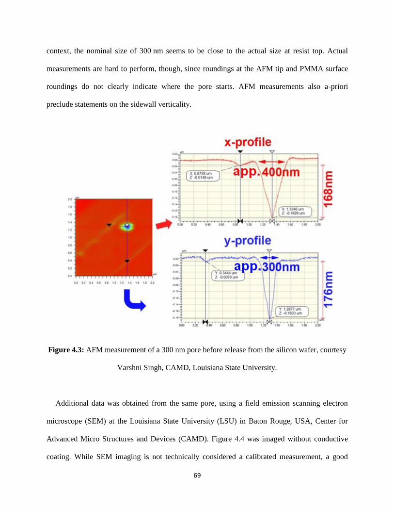
69
context, the nominal size of 300 nm seems to be close to the actual size at resist top. Actual
measurements are hard to perform, though, since roundings at the AFM tip and PMMA surface
roundings do not clearly indicate where the pore starts. AFM measurements also a-priori
preclude statements on the sidewall verticality.
Figure 4.3: AFM measurement of a 300 nm pore before release from the silicon wafer, courtesy
Varshni Singh, CAMD, Louisiana State University.
Additional data was obtained from the same pore, using a field emission scanning electron
microscope (SEM) at the Louisiana State University (LSU) in Baton Rouge, USA, Center for
Advanced Micro Structures and Devices (CAMD). Figure 4.4 was imaged without conductive
coating. While SEM imaging is not technically considered a calibrated measurement, a good

70
approximation of actual sizes can still be obtained. The image reveals that the pore does not have
a perfectly round shape, and is slightly oval. It is wider than high in this graphical
representation, but not as deformed as alluded by the convoluted data obtained using an AFM
tip. The surface size is approximated to be within 30 nm of the nominal diameter, with a width of
320 nm 5 nm and a height of 292 nm 5 nm. Further imaging with modified contrast and
brightness settings did not reveal any obstructions within the pore further down in the resist, but
did not allow for measurements down in the resist.
Figure 4.4: SEM image of the same 300 nm pore in a 1 μm thick PMMA membrane before
release from the silicon wafer, courtesy Varshni Singh, CAMD, Louisiana State University.
4.1.1. Fine tuning the Diameter of Single Pores
Under the given geometrical and lithographic conditions, minimum pore diameters using the
EBL technique available for this research are about 200-300 nm. This would suggest an
application for the detection of particles in the 100 nm to 150 nm range. Those biomolecules

71
with much smaller diameters would however require smaller pores. Many biomolecules feature a
diameter of about 10 nm. These would best be measured with pores of approximately 20-25 nm
in diameter. EBL will not readily allow to pattern a 20 nm pore in 1000 nm thick membrane.
This would equate to an aspect ratio of 50:1 and is far beyond typical limits. Optimized writers,
substrates, and processing would be required. However, the use of polymer membranes offers an
elegant opportunity to postprocess the EBL-patterened pores. To create a smaller pore, an
optional post-processing technique is, therefore, developed in this study for fine-tuning the
diameter of the pores. If applied, this processing step will follow later on in the fabrication
sequence after the membrane has been released from the wafer and integrated into the support
ring. To give a consistent overview of the nanopatterning of the pore, however, the
postprocessing option is further described here.
Such a reflow process can be performed without compromising the structural integrity of the
membrane. In the case of round pores, this reshaping can significantly reduce the pore diameter.
We introduced the surface energy model in chapter 2.2 which theoretically describes this fine
tuning process. The published procedure is modified for implementation using UV exposure
rather than electron beams. In chapter 2.2, boundary conditions were developed which have to be
satisfied in order to reduce the pore diameter upon exposure. These conditions are met for the
EBL patterned pores in this research. As an example, a 450 nm pore was shrunk by about an
order of magnitude to a diameter of approximately 22 nm: Under the impact of an intense,
broadband UV point source using a mercury vapour lamp without additional filters
(OmniCure 1000, EXFO Life Sciences, Mississauga, Canada), exposure with an intensity of
3600 mW/cm2 for a few second results in repeatable pore size reduction. Process parameters

72
were developed in iterative attempts until the above mentioned dose resulted in the size quoted.
Further details will be given in chapter 5.1.
4.2. Fabrication of Auxiliary Device Components
According to the detector system designed in chapter 3, each detector consists of the patterned
membrane as well as six auxiliary components. These additional components are two electrolyte
reservoirs, two support rings to support and protect the membrane from either side, and two
stands to support the entire detector system. Figure 3.6 in chapter 3 gave an overview, and
Figure 3.7 specified details and dimensions. These components are milled using conventional
machine shop tools. The components are thoroughly cleaned in an ultrasound-supported bath
with de-ionized water to remove all debris created during fabrication.
4.3. Detector System Integration
The patterning of the membrane was carried out on a sacrificial silicon wafer to ensure
reliable and repeatable process conditions, including flat surface topography and definite
positioning in the EBL writer. In operation, this silicon wafer will have to be removed as it
blocks the submicron pore. While releasing the membrane from the wafer, high mechanical and
thermal stresses are likely to appear, depending on the release process selected. Either might
compromise or even rupture the membrane. Additionally, the membrane might simply roll up
upon release from the wafer due to a non-uniform stress distribution. Once rolled-up, a 1 μm
thick membrane will not be usable anymore. Therefore, prior to the release process, the
membrane must get supported properly. This is achieved by attaching a PMMA support ring
onto the membrane. Considerations for the support were already commented on in chapter 3.2.4
and include:

73
The PMMA support ring must be rigid enough to support the membrane and thin enough
to avoid trapping of bubbles during filling with electrolyte. With a central hole of 1 mm, a
thickness of 300 μm was selected as a compromise.
The central hole in the support ring has a diameter of 1 mm. This dimension determines the
size of the freely suspended membrane. The submicron pore is supposed to be in the center
of the 1 mm hole. This allows for a tolerance of ring misalignment on the membrane as
well as excess glue emersion of up to 500 μm.
Attaching the support ring entails alignment to the patterned membrane, mounting, and
hermetically sealing. The overall error budget is 500 µm.
The alignment of the support ring to the nanopore is a challenge among others because the
nanopores are beyond the diffraction limit and therefore cannot be detected optically. Alignment
holes of 100 µm diameter as designed in chapter 3, Figure 3.7, and repeated in Figure 4.5 (left),
are used. The alignment groove illustrated in the same Figures is placed onto all 4 alignment
holes simultaneously, using a stereo microscope for inspection. The desired result is sketched in
Figure 4.5 (right).

74
Figure 4.5: Schematic illustration of a single pore and four 100 µm alignment holes in the
membrane (left) and of an alignment circle on the support ring (center). Aligned assembly
(right). Sketches are not to scale.
For the 75 samples assembled, the observed misalignment usually was less than 100 μm and
never exceeded 300 μm. This leaves an error budget of 200 µm to 400 µm for excess glue later
on in the integration process:
An additional challenge was to attach the aligned support ring to the membrane while the
membrane is still mounted onto the silicon wafer. In many MEMS systems, it would be
sufficient to just attach the ring so that it adheres. In the case of an electrophoretic application,
however, it must be guaranteed that not even a single nm-sized particle can pass between
membrane and ring, or else any detector signal would become obsolete. In other words, a
hermetic seal is needed between membrane and ring. This seal must also be process-compatible,
i.e. withstand subsequent processing steps. It must be transparent not to impede the optical
alignment process. And it must be proven to be biocompatible so the assembled device may still

75
be used for biomedical applications. Thermally connecting the two PMMA surfaces would
compromise the nanostructure in the membrane. Therefore, gluing the components together is
the approach of choice. Preliminary studies were carried out to find a process- and
biocompatible, transparent, hermetically sealing glue that does not drag into the pore. Two
components glues were not successful due to the high typical viscosity and long curing times.
The first impedes a hermetical seal and the second prevents stopping the drag flow of the glue
once it gets critically close to the pore. Therefore, another class of glues that features a very low
viscosity and solidifies immediately when needed was tested. These are UV initiated glues that
harden upon UV exposure. This glue first quickly flows, under the impact of capillary pull, to all
areas of interest and hence creates a complete film and hermetic seal. Once all areas of interest
are filled, further progress can be stopped by exposing the glue for a few seconds. This
immediately increases the viscosity and eventually leads to solidification. This approach protects
the pore from getting clogged with glue. Unwanted emersion of glue is also limited by the inner
edge of the support ring. While capillary forces will drag the glue through the thin gap between
membrane and ring, at the inner edge, this capillary pull ends.
In this research, we used the meth-acrylate-based photo-initiated glue Dymax 191-M. It has
biocompatibility approval, USP class VI. The UV point source previously described,
Omnicure 1000, was equipped with a band-pass filter for wavelengths from 320 to 500 nm and
positioned 5 cm from the target area. Full solidification was achieved after 10 seconds. Such
exposure heats up the membrane, potentially deforming it. Exposure conditions must therefore
take into account the solidification as well as the thermal process. If longer exposure times were
required, multi-step exposures could have been applied to ovoid thermal effects.

76
The situation after aligning and attaching the support ring to the patterned membrane is
graphically represented in Figure 4.6 A.
The next processing step is to release the sandwich of membrane and support ring from the
sacrificial silicon wafer. Three potential options are:
Back-side etching of the sacrificial silicon substrate: Selectively dissolving the silicon
substrate can be achieved using a 30 % potassium hydroxide (KOH) solution at T = 80°C
in about 7-10 hours. This option is not suitable in our system since it appeared that minor
impacts to the PMMA pore were observed. These were impacts on the nanometer scale,
potentially related to thermal effects or swelling, and those would not likely be an issue in
most other applications.
Etching of a sacrificial intermediate layer between film and silicon substrate: This
approach requires the deposition of an additional interface layer before the deposition of
the polymer at the beginning of the process sequence. For example, titanium (Ti) can be
used as such a layer and selectively get etched with hydrofluoric acid (HF). Dissolving the
intermediate sacrificial titanium layer using a 5% solution of HF 50% at T = 20°C suffers
from the extremely slow etch progress along the thin Ti layer. Up to weeks of processing
time were required in initial tests, depending on the layout.
Capillary force release: Releasing the sandwich from the silicon substrate using capillary
force rather than etching any layer is the third option. Once a tiny area starts to separate
from the substrate, further delamination is supported by capillary forces since the sample is
submersed in de-ionized water. Gentle cycling between two moderate temperatures (20°C
and 80°C) adds slight thermal stress and helps with the delamination. This option seems to

77
offer a very gentle release and therefore is considered the best approach for our fabrication
process.
Therefore, release of the membrane-support ring sandwich is performed by capillary forces.
The process was supported reducing the surface tension with the bio-degradable, non-ionic
surfactant Triton X-100. It contains Iso-octyl Phenoxy Polyethoxy - ethanol and Ethyleneoxide.
Typically after a few hours of gentle thermal cycling in 10 min intervals, the membrane detached
from the silicon wafer. The upper temperature of 80°C is below the glass transition temperature
of bulk PMMA (Tg > 100°C) and therefore save to apply without permanent deformations to be
anticipated. However, since UV treatment of the PMMA membrane is applied prior to release,
and since such treatment is known to reduce the glass transition temperature, this upper
temperature might actually be a little high and contribute to pore reshaping observed after release
as discussed in chapter 5.2 Future experiments will be carried out with reduced temperatures
[64].
The release procedure nevertheless delivers freely-suspended, patterned PMMA membranes
protected by an acrylic support ring on one side, as illustrated in Figure 4.6 B.
In a subsequent step, an acrylic support ring, similar to the one already attached to the top
surface of the membrane, is glued to the other side of the membrane in order to prevent the
freely-suspended PMMA membranes from mechanical scratching during the next fabrication
steps (Figure 4.6 C).

78
Figure 4.6: Schematic representation of the steps involved in the release of the patterned PMMA
membrane from the sacrificial silicon wafer: (A) A PMMA support ring is actively aligned and
UV glued to the membrane; (B) The sandwich of support ring and membrane is released from
the silicon wafer by capillary forces and thermal cycling; (C) A second PMMA support ring is
UV glued to the back side of the released sandwich.
In the last integration step, the support ring-membrane-support ring sandwich is assembled
with two reservoirs and two stands to form a complete electrophoretic flow detector system. The
reservoirs and their stands were introduced and specified in chapter 3.2.3. The assembly of the
final detector components is achieved using the same UV glue introduced above. Figure 4.7
shows a picture of such an assembled electrophoretic flow detector device with an overall length
of 33.6 mm. Each reservoir has a filling capacity of about 0.45 ml and contains an upper inlet.
These inlets will allow to introduce electrolyte and electrodes in preparation of experiments. The
horizontal orientation of cylindrical reservoirs and vertical orientation of the membrane reduces
the pressure on the membrane during filling of the electrolyte, facilitates electrolyte filling

79
without formation of bubbles, and also allows for identical positioning of the electrodes with
respect to the pore. Electrodes are placed approximately 5 mm apart from the PMMA membrane
through the upper inlets. The freely-suspended PMMA membrane in the center contains a
nanometer-scaled pore which forms the only permeable component of the whole detector device.
Figure 4.7: Micrograph of a complete, all-PMMA electrophoretic flow detector device.
4.4. Self-Assembly of α-hemolysin Protein Pores
In the previous chapters it was discussed how pore diameters down to a few hundred
nanometer are fabricated by EBL using a top-down fabrication approach. If smaller pores are
needed, the pores are post processed exploiting surface tension to decrease the pore size by one
order of magnitude. Pore diameters of 20-25 nm can then get reliably fabricated. Our current
micro and nano fabrication sequence does not allow to fabricate pores that are yet 1 order of
magnitude smaller. However, in order to detect single stranded nucleic acid (ssDNA), pore
diameters of about 1.5 nm would be needed.
While working on further improvements of top-down nanofabrication sequences in PMMA, a
bottom-up approach was developed to generate 1.5 nm pores in the PMMA detector system. This

80
alternative exploits naturally occurring protein pores. It therefore somewhat diverts the all-
PMMA concept and also reduces the size expectancy of the diameter. But it allows testing the
system as a whole and predicts future performance when the protein pores will be replaced by
artificial ones. In this rapid prototyping approach, α-hemolysin protein pores were selected, and a
fabrication sequence was developed to allow integration of such pores into a PMMA system.
α-hemolysin protein pores have been extensively employed over the last decade for probing
the structure and dynamics of biomolecules such as single-stranded nucleic acids (ssDNA) under
a range of experimental conditions [10, 65, 66]. Such protein pores have been previously
integrated into silicon-based systems [67], while we now develop a technique to allow for their
implementation into a polymer micro-device.
In a first step, a lipid bilayer membrane is suspended across a hole in a PMMA layer.
Subsequently, a protein nanopore is introduced directly into the suspended lipid bilayer
membrane. Since the forces involved in the process of attaching the lipid bilayer membrane to
the PMMA are comparatively high, the PMMA layer needs to be more robust than the 1 µm
membrane applied so far. Instead of using a spincoated membrane, we now directly apply the
micro machined PMMA ring of 300 µm thickness as a support structure. The inner hole, which
previously was 1 mm, needs to be reduced to 100 µm to alleviate stress on the lipid bilayer to be
mounted later on. Since mechanical microfabrication results in burs and other artifacts that could
compromise the vulnerable lipid bilayer, an acrylic ring is first prepared with an inner diameter
of 200 µm. This hole is then exposed to a post processing sequence similar to the one used to
reshape EBL patterned nanopores: The PMMA hole is exposed to an intensity of 3600 mW/cm2
for a few ten second in a broad band UV spectrum from 250 nm to 650 nm. As explained in
chapters 2.2 and 4.1.1, surface tension will smoothen the rim of the pore and shrink its diameter

81
to about 100 µm. The post processed ring is then integrated in to the detector system as described
in chapter 4.3. Finally, the lipid bilayer and the α-hemolysin pores are added: A lipid bilayer
membrane is formed across the prepared micropore by dipping a paintbrush into a lipid solution
and painting across the micropore as described by Stefureac et al. [14]. This comparatively
forceful process is the reason why a PMMA ring is used instead of a thin membrane. The lipid
solution is purchased from Avanti Polar Lipids Inc. (Alabaster, AL), vacuum-dried for 4 hours,
and re-dissolved in decane to a final concentration of 30 mg/ml of lipid. Formation of a stable
lipid bilayer membrane across the micropore is identified by a complete blockage of the open
pore current Iopen through the micropore in the acrylic layer, when tested in a patch clamp setup.
In the final step, the pre-formed lipid bilayer membrane provides support for the protein
nanopores of α-hemolysin. α-hemolysin pores, purchased from Sigma-Aldrich (St. Louis, MO),
are prepared to a solution with the final concentration of 1.25 µg/ml. Using a pipette, these α-
hemolysin pores in solution are now self-assembled into the prepared lipid bilayer membrane by
injecting a total of 5 µl of above protein nanopore solution adjacent to the micropore in the
PMMA layer. Performed during patch clamp testing, protein pore insertions and their self-
assembly are immediately detected by a characteristic jump in the Iopen value. According to
Stefureac et al. [14], each inserted protein pore results in an Iopen value of approximately 100 pA,
when an external potential of + 100 mV is applied across the membrane.
In chapter 4, a complete fabrication process for an all-PMMA electrophoretic flow detector
for biological applications was proposed. Cylindrical pores were microfabricated in PMMA
membrane using electron beam lithography. Auxiliary components of the detector were
fabricated using conventional machining techniques. An optional post processing procedure was
introduced to fine-tune the pores, reducing the diameter by one order of magnitude as required

82
by selected biological applications. The entire detector system was aligned and assembled using
UV-initiated glue. An alternative fabrication sequence is based on self-assembly of biological
protein pores.

83
5. Detector Test Results and Discussion
After explaining the design and the fabrication of detector devices in the previous chapters,
the detectors now need to be tested. In this chapter, the functionality of the detector devices is
evaluated using both, test nanoparticles and two different biomolecules. The initial steps in
testing such detector devices are determining the actual pore size, verifying the nanofluidic
integrity of the entire system by analysing the open-pore current, and calibrating the detectors by
evaluating the current blockade induced by nanoparticles of known sizes. At the end, the two
biomolecules are detected and their translocation dynamics are compared with each other.
5.1. Patch Clamp Test Setup
The electrochemical chambers discussed in the previous chapters were fabricated and
assembled using different pore sizes between 1.5 nm and 450 nm. To be used as an
electrophoretic detector, an electrolyte needs to be added along with two electrodes. A power
supply delivers precise, constant, and adjustable voltage levels. Picoammeters with response
times better than milliseconds are needed in an environment that is preferably
electromagnetically shielded. In our lab, we used a setup as illustrated in Figure 5.1. It consists of
an amplifier (Axopatch 200B, Axon Instruments) which provides electric potential range from -1
to +1V and also amplifies the ionic resistive pulse, a digitizer (Digidata 1440A) that acts as
analog to digital signal convertor, and a Faraday cage comprising a peltier cooled headstage
(CV 203BU) to minimize the thermal noise, the microfabricated detector device, and two
Ag/AgCl electrodes.
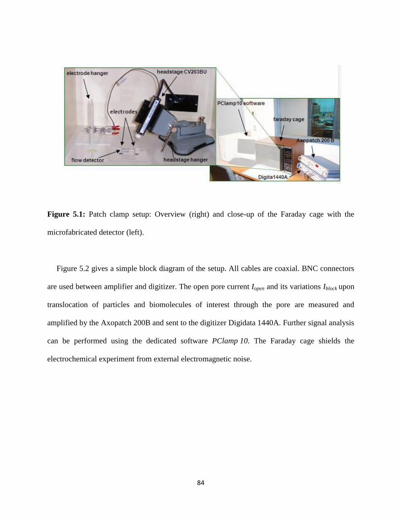
84
Figure 5.1: Patch clamp setup: Overview (right) and close-up of the Faraday cage with the
microfabricated detector (left).
Figure 5.2 gives a simple block diagram of the setup. All cables are coaxial. BNC connectors
are used between amplifier and digitizer. The open pore current Iopen and its variations Iblock upon
translocation of particles and biomolecules of interest through the pore are measured and
amplified by the Axopatch 200B and sent to the digitizer Digidata 1440A. Further signal analysis
can be performed using the dedicated software PClamp 10. The Faraday cage shields the
electrochemical experiment from external electromagnetic noise.

85
Figure 5.2: Patch clamp setup block diagram
5.2. Characterization of the Pore Geometry
A standard tool in measuring microscopic feature sizes is optical microscopy. Diffraction
limits the resolution of optical microscopes to a few hundred nanometers. Many of the pores
fabricated can therefore not even be imaged, and none measured with sufficient resolution.
Diffraction effects can be neglected in Electron microscopy, and details down to nm or even sub-
nm scale can be imaged. Given the relatively thick membrane, transmission electron microscopy
cannot be applied for such a small feature size. However, as it was discussed in chapter 4, SEM
as non-calibrated and AFM as calibrated methods can be used within limits to measure the pore
size before releasing from silicon wafer. However, SEM measurements always led to thermal
damage of the membrane surface, and AFM results suffered from convolution effects.

86
Since the release of the membrane from sacrificial substrate will also have an impact on the
exact pore size, it should be remeasured after release. At this stage, even worse thermal effects
are expected from SEM inspection since the sacrificial wafer no longer serves as a heat sink, and
the AFM tip would likely mechanically compromise the membrane as it is no longer supported
from the back side. An alternative to using such standard metrology tools is to evaluate the nano-
fluidic performance of the pore. This approach allows to assess the effective pore diameter
regardless of whether this is located at the top of the membrane, at its bottom, or in between.
This constitutes a further advantage over standard tools which are often limited to measuring
surface topographies. The pore diameter was derived in chapter 2, under the assumption of a
cylindrical pore, as
(5.1)
where D is the pore diameter, L denotes the length of the pore, corresponding to the membrane
thickness, U is the voltage applied across the membrane, I is the current through the pore, and K
is the specific conductivity of the KCL solution. This equation allows to do electrochemical
measurements with the pore to approximate its size and to reliably compare pore sizes with a
constant measurement setup.
Based on equation 5.1, the 300 nm pores previously inspected by SEM and AFM delivered a
diameter of 450 nm. The observed mismatch might indicate a change of the diameter between
the previous measurements performed on a sacrificial substrate and the current measurement
performed after release. In particular, the UV exposure and thermal cycling could have

87
contributed to such a change. Furthermore, the electrochemical measurements might slightly
overestimate the diameter based on the applicability of the underlying model assumption of a
cylindrical pore shape.
5.3. Analysis of the Open Pore Current
After determining the exact pore size, the nanofluidic detector functionality is now verified by
analyzing the open pore current Iopen. These tests will be used to evaluate whether the detector
system is hermetically sealed and the only connection between the electrolyte reservoirs actually
is the nanopore. This would be a requirement for any application as a pore-based detector. Tests
also include an electrochemical characterization of the detector, analyzing the followings:
Noise levels of unpatterned membranes;
Long-term stability and noise levels of the open pore current Iopen;
Current-voltage (I-V) characteristics;
Impact of electrolyte concentration on Iopen and the cross-pore conductance;
Impact of electrolyte concentration on resistance of the pores.
In all experiments, both electrolyte reservoirs are filled with KCl electrolyte solution of 0.1 M
concentration, unless otherwise stated. An unbuffered KCl solution with a slightly acidic pH
value of 6.0 ± 0.2 is used in all experiments to avoid introduction of variations, which might
otherwise potentially lead to additional ionic effects in the system.
5.3.1. Noise Level of unpatterned Membranes
Selected tests were carried out with a complete flow detector system, however using an
unpatterned membrane, i.e. a membrane without a pore. This test was made for few times over a

88
period of a day. A reliable detector would therefore deliver an “open pore current” of zero,
independent of properties such as the electrolyte concentration or the acceleration voltage. These
tests, if successful, will validate the hermetic assembly concept, the dielectric properties of the
membrane, and the system noise level in the absence of fluidic effects.
The measured open pore current actually was zero for all devices and under all conditions
tested. This proves a hermetic seal of the devices. Typical noise levels are between 4 pA and
5 pA at 2 kHz bandwidth. This noise does not include contributions from fluidic effects and is
referred to as system noise. It arises from the electrodes, the electronic instrumentation (e.g.,
voltage clamp amplifier), external sources (e.g., power lines, fluorescent lights, monitors, and
even noise associated with mechanical vibrations), and the digitizer. The faraday cage mentioned
in chapter 5.1 shields the electrophoretic setup. The Axopatch system is equipped with an 8-pole
Bessel low pass filter with a -3 dB selectable bandwidth of 1 kHz to 100 kHz, and built-in
amplifiers are optimized for low noise in the DC to 10 kHz bandwidth. According to the
manufacturers’ users guide [7], the lowest noise level that can be achieved is less than 1 pA. This
is about 20% of the noise we determined for the entire system in the laboratory environment.
5.3.2. Long-Term Stability, Noise Level and Repeatability of the Open Pore Current
In subsequent tests, 450 nm pores are characterized electrochemically. Figure 5.3 exemplifies
sample recordings of the open pore current Iopen in 20 mV increments of the applied voltage
(20 mV to 100 mV) over a time period of 10 minutes. The ionic transport at 20 mV applied
external voltage is magnified in the left inset to better demonstrate the presence of a steady-state
Iopen of 4 nA and the corresponding noise of 25-30 pA. at 100 mV, Iopen increases to 20 nA with a
10 kHz noise of 35-40 pA (see right on the right).

89
Figure 5.3: Patch clamp measurements of the open-pore current (Iopen, nA) through single
cylindrical submicron pores (300 nm diameter) in PMMA membrane as a function of time (min),
in the presence of 0.1 M KCl electrolyte solution and applied external voltages of 20 mV to
100 mV, in 20 mV increments. The magnified insets demonstrate a steady-state Iopen over time at
20 mV applied voltage having a low level of noise (approx. 1% of Iopen). The measured signal is
reproducible within ±10-15% shown with error bar.
The observed noise is less than 1% of Iopen for all voltage levels analyzed. However, it is still
significantly more than the system noise of 4-5 pA introduced in the previous chapter. Additional
sources of noise related to fluidics depend on parameters affecting the fluidics and surface charge
properties. Such parameters include the electrolyte concentration, the pH value, the
electroosmotic flow, and the driving voltage. The detected noise also depends on the filters
applied in the measurements. A filter with appropriate band width reduces noise to a level
deemed acceptable so that the desired signal can be detected. A wider filter band width can be
chosen if the signal is large enough compared to the background noise, so that more rapid events

90
can pass through the filter. In our experiments, we used a filter band width of 10 kHz, which is
commonly used in patch clamp experiments.
The measured signal is reproducible within ±10-15%, when the pores gets evacuated, washed
with de-ionized water, and re-examined following the same procedure after a finite period of
time. This value therefore not only comprises the variations between several measurements, but
also includes ‘reusing’ a pore that was cleaned in between uses. These variations are identified as
the error bars in Figure 5.3.
The ionic current measured appears to be independent of the exact distance between each
electrode and the membrane, as long as both electrodes are approximately placed in the same
distance from the membrane, which is guaranteed by the system layout. Measurements are
started 0.5 to 1 hour after filling the electrolyte solution to allow for the pore to reach its steady-
state Iopen level. This setting time is usually attributed to the dynamics associated with wetting of
the pore and also removal of contaminant layers; contaminants from previous measurements, as
well as contaminants in the electrolyte solution, would certainly add to the overall noise level.
Both should therefore be minimized, and the setting time addresses at least the first point. In the
present research, the setting time is significantly reduced by immersion of the pores into de-
ionized water for storage immediately after each experiment. This is shown to avoid drying of
the pores as well as accumulation of solidifying contaminants in the vicinity of the pores.
The detector devices are tested over a period of three months (some even up to a year) to
show their long-term and multi-experiment stability.
The low level of noise would, of course, likely increase with a significant decrease in the pore
size because of an increase in the relative tolerance and roughness and an increase in the effect of
contaminants and their relative importance. Furthermore, Siwy et al. [40] demonstrated that the

91
ion transport properties of artificial micro/nanopores are strongly influenced by the chemical
structure of the membranes as well as microfabrication steps involved, including beam exposure
and other accompanying pore development procedures. For instance, the typical behaviour of the
ion current versus time recorded at a constant voltage in the case of PET membrane exhibited
pronounced fluctuations with a high level of noise. Likewise, the nanopores in PC foils present
similar transport characteristics. In contrast, there were no fluctuations observed for pores
microfabricated in PI by the same procedure of ion track etching [40, 68]. The authors explained
this difference with different material structures/properties related to imperfectly terminated
polymer chains. Upon ion exposure-induced scission of polymer chains and subsequent chemical
etching, carboxylate end groups are formed in PET. In PET, the so called “dangling ends” are
created due to the presence of ethylene components, which perform random movements and thus
fluctuations, when immersed in a solution. The chemical structure of PI, on the other hand, is
based on a planar sequence of aromatic groups, rendering a strong rigidity to the material and
limiting the movement of PI polymer chains and thus fluctuations when immersed. Smoothness
and rigidity of the PI surface thus seem to be the factors responsible for the observed stable ionic
current.
In agreement to above, we propose that the observed low level of noise with our PMMA
membrane-based detector devices can be mainly attributed to the experimental conditions that
are employed by our group in comparison to other research groups. This is because of the fact
that electron beams are also previously shown to create carboxylate end groups (dangling ends)
with a net negative charge on the surface of PMMA membrane [69]. However, we, in our
experiments, could control their formation and, thus the resulting negative membrane surface
charge, keeping them in their minimal amount using KCl electrolyte solution of a slightly acidic

92
pH value; at neutral and basic pH values, the generated dangling carboxylate end groups by the
microfabrication/micro-patterning procedure are deprotonated, yielding in an excess negative
charge attached to the relatively flexible polymeric chains on the membrane surface. Under these
circumstances, when a micro/nanopore is immersed in an electrolyte solution, increasing the
voltage and, thus enhancing the electric field, will cause the negatively charged flexible dangling
end carboxylate groups to move vigorously in the field direction resulting in an increased level
of noise. In comparison, at a slightly acidic pH value of the electrolyte solution (6.0 ± 0.2) used
in our experiments, however, the carboxylate end groups are mostly kept in their protonated
state, giving rise to a minimal net negative surface charge on the membrane and, thus minimal
random movements/fluctuations under an applied external voltage. Our explanation is in
accordance to those of other researchers; Siwy et al. [40] suggested that reducing the electrolyte
pH value below 3 would neutralize carboxyl groups present on PMMA membrane surface
lowering the negative surface charge density of the membrane. However, this could destabilize
our analyte molecules to be detected in our next experiments and is hence not a feasible option.
In any case, the preceding arguments all stress the importance of fine-tuning the surface
chemistry of membranes in the operation of micro/nanopore systems and their associated noise
level. Other than the described reversible changes (reduction of net negative surface charge) in
membrane surface chemistry caused by manipulation of the pH of electrolyte solution, in which
the pore-containing membranes are immersed, another approach could be through chemical
surface modification procedures, which can be implemented relatively easy on polymer
membranes: a huge advantage for our selected membrane material of PMMA. Whilst there are a
number of existing physical and chemical methods, in the area of surface modification of
polymeric synthetic membranes most emphasis has been given to plasma treatment, grafting of

93
polymers on the surface, and modifying the surfaces by adding surface modifying molecules [38,
70].
Summing up the measured results of this chapter, the pores exhibit a stable, time-independent
open pore current with a low level of noise over a wide range of applied voltages from 0 mV
(control scenario) to 100 mV. This proves that the PMMA membrane neither deteriorates by
excessive swelling nor starts to leak over time.
5.3.3. Current-Voltage Characteristics
As anticipated from above results, evaluation of the open-pore current-voltage (I-V)
characteristics demonstrates a strong linear relationship at five different KCl electrolyte solution
concentrations of 0.02, 0.05, 0.1, 0.5, and 0.75 M (Figure 5.4). No saturation is observed for
higher driving voltages, such that a wide range of voltages from 0 mV to + 100 mV typically
used in such electrophoretic experiments can be applied. Even further increasing the
transmembrane potential to voltages beyond + 100 mV does not damage the PMMA membrane,
and further increases the current through the submicron pore to higher values. This is in contrast
to protein nanopores, such as α-hemolysin, where a transmembrane potential of + 100 mV
produces a current value of approximately 100 pA, but a higher potential will result in damage to
the lipid bilayer membrane [18].
The observed I-V characteristics in Figure 5.4 are linear and do not show any current at an
applied driving voltage of zero. This relates to the transport mechanisms effective in our devices
(no diffusive contribution), and determines that it is possible for our devices to operate under
reverse polarity. Three different transport mechanisms can contribute to the measured total
steady-state ionic transport through a specific pore: convection i.e., electro-osmotic flow (EOF),
driven by the pre-formed electric double-layer on the pore surface and walls (explained in

94
section 5.3.4), and partly by the electric field applied across a pore] (Ho et al., 2005),
electrophoretic ion migration (driven by the electric field applied), and diffusion (driven by the
electrolyte concentration gradient). Diffusion is the only contribution independent of the applied
voltage. The devices exhibit zero current at zero voltage, indicating negligible diffusive transport
contributions. Therefore, as expected, the electrolyte solution does not exhibit a concentration
gradient across the pore for either of the tested molarities.
Figure 5.4: Patch clamp measurements of Iopen (Io, nA) as a function of the applied voltage (mV)
for five different KCl electrolyte concentrations of 0.02, 0.05, 0.1, 0.5, and 0.75 M.
As shown in Figure 5.4, the same linear I-V relationship is maintained when negative
transmembrane potentials of 0 mV to -100 mV are applied. More accurately, the amount of
-100 -80 -60 -40 -20 0 20 40 60 80 100-60
-40
-20
0
20
40
60
V(mV)
Iop
en
(nA
)
0.1 M
0.05 M
0.02 M
0.5 M
0.75 M

95
current measured through the pore at a certain negative transmembrane potential is
approximately the same as that measured at a corresponding positive potential. These pores,
therefore, do not exhibit rectification of the current flowing through them. Similar I-V
relationships have been reported by other groups working with cylindrical nanopores [71, 72,
34]. This observation has two implications: First, the device can be operated in either direction
(or polarity), which is referred to as dual "on"-state (see below for explanation). Second, this is a
further confirmation of the symmetrical shape of our pores: asymmetric (e.g. conical) pores such
as basically all protein pores and conically-shaped artificial synthetic pores typically exhibit
current rectification. This can be explained by a model focusing on electrostatic interactions
between ions passing through a specific pore and the surface charge distribution on the pore
surface and walls [50]. Almost all microfabrication processes and their accompanying pore
development steps leave artificial nanopores in either polymer membranes or silicon-based
substrates with a net negative charge on their surface and walls [40]. The surface charge creates
an asymmetric internal electrostatic potential inside the pore with a profile dependent on the pore
shape. Conical pores accumulate a much higher negative charge, and thus formation of a stronger
electrostatic trap, on the pore base compared to the pore tip. This stronger electronic trap, with
the applied transmembrane potential induced by the electrodes, creates a preferred transport
direction for positively charged ions towards the base [73, 74, 75, 76, 38]. As asymmetric
nanopores tend to reduce the ionic flow in one direction, but promote it in the other, they are said
to be either in the “on” state with much higher currents flowing through the pores, or in the “off”
state with much less currents flowing through the pores. Artificial conical nanopores could,
therefore, act like “voltage-gated” channels, resembling some of their biological counterparts.
The gated channels open (on state) and close (off state) in response to a specific chemical,

96
mechanical, or electrical signal. This phenomenon, however, does not occur in symmetric
submicron pores with a homogenous surface charge distribution inside the pores, just like for the
pores presented in this study. It is often considered an advantage for such pores to be always in
their “on” state of function regardless of the polarity of the applied transmembrane potential.
5.3.4. Impact of the Electrolyte Concentration on the Open Pore Current and the Cross-
Pore Conductance
The electrical characterization of our detector devices is expanded to the Iopen as a function of
the electrolyte concentration. It is shown in Figure 5.4 that the current monotonously increases
with increasing KCl electrolyte concentration (0.02 M to 0.75 M) in an almost linear
relationship. Applied voltages range from + 10 mV to + 100 mV.
Standard electrolyte concentrations for biological experiments range from approximately 0.75
down to 0.1 M. Higher electrolyte concentrations are avoided in their experiments because of
biological pore are being saturated. They are usually shown to saturate, reaching a conductance
plateau, when the concentration is raised above a certain physiological level. This has been
attributed to a limited binding-unbinding capacity for protein nanopores. In comparison, artificial
synthetic micro/nanopores in solid-state membranes do not exhibit such a saturated conductance
pattern, allowing their application in a broader concentration range. We also identified that the
dependence of the ionic current through single artificial submicron pores on the electrolyte
concentration deviates to a curve with a steeper slope, at all the voltages applied, as the
electrolyte concentration is lowered to values below 0.1 M. We therefore extended the
electrolyte concentration range in our tests beyond 0.1 M and included 0.02 and 0.05 to study the
flow behavior in this critical region as well. The results obtained are in agreement with Schiedt et
al. [50] (Figure 5.5). The observed phenomenon has been attributed to two effects: an incomplete

97
dissociation of the electrolyte at higher concentrations, and formation of an “electric double-
layer”. An electric double-layer is formed as the negative surface charge on the PMMA
membrane, due to the formation of carboxylate end groups, attracts K+ ions in the electrolyte
solution to the pore surface and walls [50, 41]. The electric double layer, then increase the
effective potential for the electrochemical transport mechanism through the pores. The thickness
of the formed double-layer depends on the salt concentration of the electrolyte solution in the
vicinity of the membrane; at lower salt concentrations, the relative concentration of K+ ions on
the pore surface and walls is much greater compared to that in the bulk electrolyte solution,
determining a thicker double-layer, and therefore an elevated conductivity gradient or higher
conductance.
Figure 5.5: Patch clamp measurements of Iopen as a function of the KCl electrolyte concentration
for the applied voltages ranging from 10 mV to 100 mV.
0 0.1 0.2 0.3 0.4 0.5 0.6 0.7 0.80
10
20
30
40
50
60
KCl Concentration(M)
Io (
nA
)
100 mV
90 mV
80 mV
70 mV
60 mV
50 mV
40 mV
30 mV
20 mV
10 mV

98
The same effect is illustrated in Figure 5.6 by showing the conductance [reciprocal of the
steady-state pore resistance (1/Rp), ns, demonstrated below] measured as a function of the
electrolyte concentration. In accordance to the data presented above, the pore conductance also
over-proportionally increases with increasing electrolyte concentration at low concentrations.
Our results are in close agreement with those reported by other researchers fabricating
cylindrical and conical nanopores in membranes with unique surface charges [34, 50].
As a remedy to this effect, the negative surface charge on the membrane can be minimized or
even neutralized by temporary protonation of the membrane surface, which offers additional
positive charge carriers, or by modification of the surface properties themselves permanently or
for intermediate terms. Temporary protonation can be achieved by adjusting the pH value of the
electrolyte solution to an acidic regime [40]. We, ourselves, observed a pH value of
approximately three to almost neutralize the aforementioned effects. However, whether such an
approach is compatible with future biological experiments might need further clarification.
Modification of the surface properties of the membrane can be achieved for longer times by
either inducing chemical reactions based on oxygen plasma treatment or by photochemical
modifications involving UV surface exposure [38, 77].
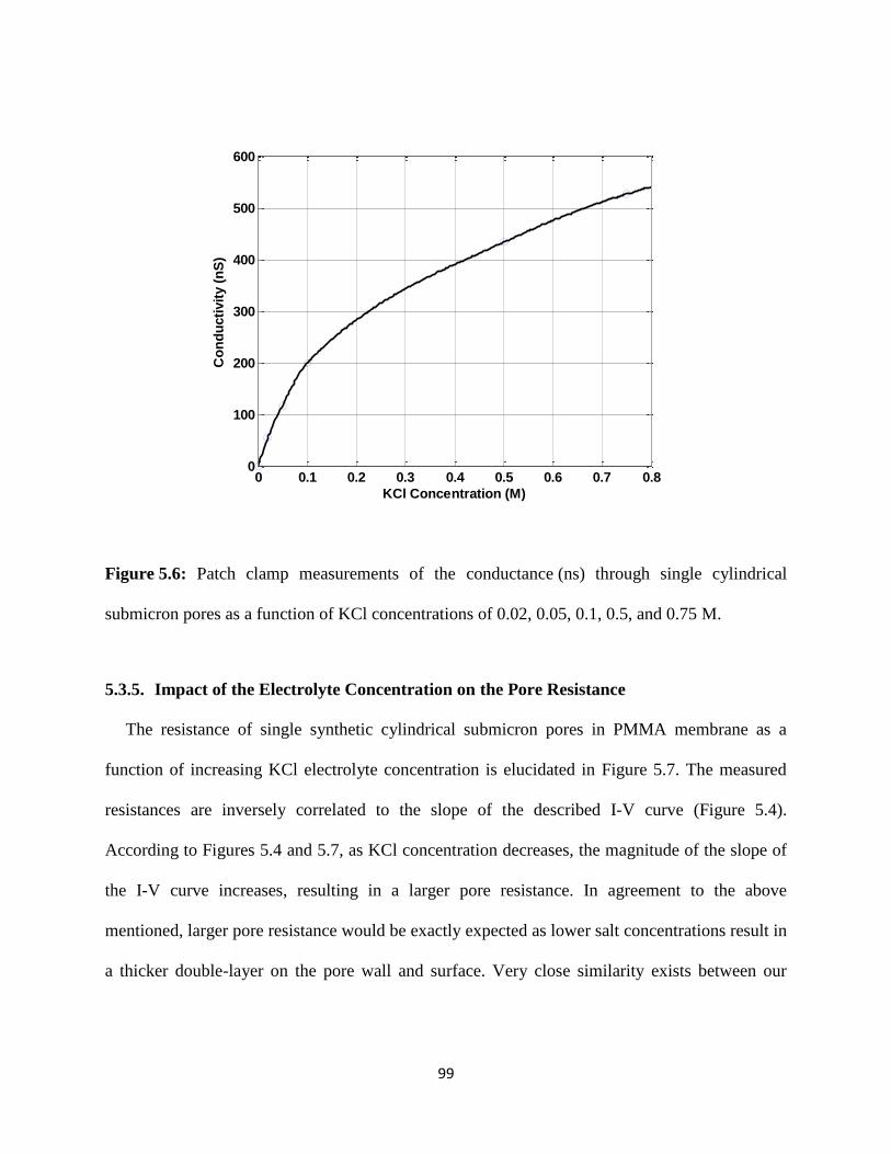
99
Figure 5.6: Patch clamp measurements of the conductance (ns) through single cylindrical
submicron pores as a function of KCl concentrations of 0.02, 0.05, 0.1, 0.5, and 0.75 M.
5.3.5. Impact of the Electrolyte Concentration on the Pore Resistance
The resistance of single synthetic cylindrical submicron pores in PMMA membrane as a
function of increasing KCl electrolyte concentration is elucidated in Figure 5.7. The measured
resistances are inversely correlated to the slope of the described I-V curve (Figure 5.4).
According to Figures 5.4 and 5.7, as KCl concentration decreases, the magnitude of the slope of
the I-V curve increases, resulting in a larger pore resistance. In agreement to the above
mentioned, larger pore resistance would be exactly expected as lower salt concentrations result in
a thicker double-layer on the pore wall and surface. Very close similarity exists between our
0 0.1 0.2 0.3 0.4 0.5 0.6 0.7 0.80
100
200
300
400
500
600
KCl Concentration (M)
Co
nd
ucti
vit
y (
nS
)

100
present data and the ones reported by other researchers fabricating cylindrical nanopores in
silicon-based membranes [33].
Figure 5.7: Resistance of single submicron pores (Rp, MΩ) as a function of increasing KCl
concentrations of 0.1, 0.5, and 0.75 M.
5.4. Functional Analysis of Submicron Pores via Translocation of Differently-Sized Silica
Nanoparticles
In section 5.2, the geometrical pore properties were identified. In section 5.3, the nanofluidic
detector functionality was verified by analysing the open pore current. A third aspect of pre-
testing the flow detector now is calibrating it by measuring the current blockage caused by nano
particles of known size. Test objects are silica nanospheres of 100 nm and 150 nm nominal
0 0.1 0.2 0.3 0.4 0.5 0.6 0.7 0.80
5
10
15
20
25
30
KCl Concentration (M)
Resis
tan
ce(M
oh
m)

101
diameters purchased from Polysciences, Inc. These are tested in pores with a nominal diameter
of 300 nm and an actual diameter of about of about 450 nm.
In preparation of the test are the electrolyte reservoirs of filled with electrolyte solution of 0.1
M concentration, using unbuffered KCl with a slightly acidic pH value of 6.0 ± 0.2. The test
nanoparticles are then added to the reservoir on the negative side of the membrane (cis
compartment). The final concentration is 3.109 spheres/ml. An external potential between 10 mV
and 30 mV is applied across the membrane to induce a transmembrane ionic current.
5.4.1. Mathematical Model for the Current Blockade
Prior to actual measurements, translocations of silica nanoparticles through a 450 nm pore are
mathematically modeled to obtain reference values for later experimental verification. The
temporary current blockade Iblock associated with such an event is calculated based on an increase
in resistance, ΔR, due to the presence of nanoparticle/s inside the pore. Different models have
been proposed in literature to estimate the resistance variance developed by a single particle
translocating through a pore [34, 52]. All of these models have been proven valid only for certain
and very specific pore shapes and dimensions. Deblois and Bean [52] were the first to develop a
theory for translocating spheres in a uniform electric field that is valid over a broad range of pore
shapes and dimensions. Deblois model was described in detail in chapter 2. Simplifying the
model for a cylindrical pore of diameter D, a translocating sphere diameter of d«D, ΔR can be
written as
(5.2)

102
where ρ is the electrolyte resistivity and L is the length of the pore over which the potential
difference is applied. This expression includes the Maxwellian value as its limit. The increased
resistance obtained is independent of the pore length L if L is much bigger than Dm [52]. This
applies to the geometry under discussion with L = 1000 nm and Dm = 450 nm. This means that
the obtained ΔR values in this situation can be quite the local values across the pore and is only
affected by the existing of nanoparticle inside the pore.
Deblois’s group evaluated their proposed model by calculating ΔR values for three different
pore sizes of 400 nm, 454 nm, and 500 nm diameter, and translocating sphere particles of up to
400 nm in diameter. They considered an electrolyte resistivity of ρ = 0.75 Ωm. Among all of
their analysis, it is demonstrated that the ΔR values calculated for a 454 nm-diameter pore were
in very close agreement with the experimentally obtained values for translocating sphere
particles of less than 200 nm in diameter. From above model, it is concluded, in a simplified
form, when the sphere particles get closer in diameter to that of the pore, the experimental results
of ΔR fall below the theoretical values. This ΔR value, is then used to determine the magnitudes
of the Iblock (which represents as ∆I) spikes according to
(5.3)
The particle size obviously has the strongest impact on the current blockade. Increasing
particle diameters will increase the expected blockade in a cubic fashion. Assuming a constant
driving voltage of 20 mV, 100 nm silica nanoparticles translocation through 450 nm pore result
in current blockade of Iblock = 32 pA, which is only twice the noise level, whereas larger particles
of 150 nm diameter cause a much increased blockade of Iblock = 112 pA.

103
5.4.2. Measured Current Blockade of 100 nm Silica Nanoparticles
Measurements of the ionic current through a single 450 nm wide pore are performed both in
the absence and presence of 100 nm silica nanospheres. When only pure electrolyte solution
without adding nanoparticles is present, an applied constant voltage of 20 mV induces an open
pore current Iopen of approximately 3970 pA. The signal has a very low noise level of
approximately 25 pA, and does not fluctuate over time. A typical measurement is reproduced in
Figure 5.8 A.
In the next step, 100 nm-silica nanoparticles are added to the electrolyte. Triton X-100
surfactant (0.1% w/v) is also added supporting the translocation of nanoparticles in two ways: It
reduces the surface tension in the electrolyte which promotes the wetting properties of the pore
and results in an improved flow through the pore. Secondly, the probability of adsorption of
nanoparticles to each other, onto the PMMA membrane surface and surfaces of the
electrophoretic flow detector is reduced. During extensive measurements, tens of thousands of
translocation events are recorded. Figure 5.8 B shows a typical current trace recorded in the
presence of 100 nm silica nanospheres. In contrast to Figure 5.8 A, temporary current blockades
well beyond the noise level are now observed. These are not present in the absence of
nanospeheres and can therefore be associated with individual translocation events of
nanospheres. The blockade amplitudes allow to not only detect individual translocation events,
but to also discriminate between two distinct blockade regimes: A smaller group of events
exhibit Iblock values of approximately 30 to 35 pA, while a larger group of events demonstrates
current deductions of about 50 to 55 pA.
The first group with Iblock values of 30 to 35 pA is consistent with the prediction of the
mathematical model and is therefore associated with a current signature indicative of a complete

104
translocation of 100 nm silica nanoparticle (labelled as ‘type I’ in Figure 5.8 C). On average, a
complete translocation event takes a blockade time of about 0.5 ms. Type II current signatures in
Figure 5.8 C with blockade values of 55 to 65 pA can likely be attributed to the passage of
multiple (most probably two) nanoparticles at the same time. This is likely not an independent
movement of two individual particles, but due to aggregation of multiple nanoparticles. Some
agglomeration can still occur despite the treatment with a surfactant as described above. Type II
current signatures in Figure 5.8 C demonstrate a multi-blockade fine structure labelled with
subscripts a, b, and c. This labelling refers to earlier studies by Prabhu et al. [78]. Consistent with
literature, IIa and IIc events could represent the presence of nanoparticles at the entrance of
single pores near their top surface and at the exit of single pores near their bottom surface,
respectively. These blockades therefore do not represent successful translocations but are as
unavoidable part of high interaction effects in between multiple particles and pore. IIb events
represent the presence of nanoparticles actually passing through the centre of a pore, blocking a
major portion of the baseline open pore current of Iopen. On average, a complete translocation
event through single pores for multiple (probably two) nanoparticles takes a blockade time of
about 1.5 ms. Under the same applied voltage of 20 mV, the difference in blockade times of 1.5
ms versus 0.5 ms observed with current signatures of translocation events II and I could be
explained by a higher degree of electrostatic interactions that may occur between translocating
nanoparticles and the fixed surface charges on the membrane, when multiple nanoparticles are
passing together, at the same time, through single pores.

105

106
Figure 5.8: Open pore current Iopen through a 450 nm wide nanopore in a 1 µm thick PMMA
membrane and current blockades Iblock caused by translocation events of 100 nm silica
nanospheres. Measurements obtained at room temperature, 20 mV driving voltage, and 0.1 M
electrolyte concentration: (A) Basal ionic current Iopen versus time in the absence of silica
nanoparticles as a reference; (B) Ionic current with temporary current blockades of 30 to 55 pA
in the presence of nanoparticles; (C) Close-up of a segment of B with 2,000-fold time resolution,
showing only two individual blockade events representing two types of translocation events -
type I with current blockades of about 30 to 35 pA, type II with current blockades of about 50 to
55 pA.
Translocations are measured for various driving voltages, beyond the 20 mV described above.
Figure 5.9 represents excerpts from line traces taken from the each individual experiment at
10 mV, 20 mV, and 30 mV (left to right). Two effects can be identified regarding frequency and
amplitude: Translocation events occur more frequently upon increased voltage at otherwise
constant conditions. At 10 mV, on average, a translocation occurs every 1.5 seconds, at 20 mV
every 1 second, and at 30 mV every 0.5 seconds. Besides, the amplitude of the current blockade
increases, from typically 15±5 pA at 10 mV to 30±5 pA at 20 mV to finally 40±5 pA at 30 mV.

107
Figure 5.9: Measured current signal with open pore current and current blockade events during
the translocation of 100 nm silica nanospheres through a 450 nm pore in PMMA for various
driving voltages (10 mV, 20 mV, and 30 mV).
This increase in frequency and amplitude can be explained based on a force equilibrium
acting on the nanoparticles: The driving force for a nanoparticle to translocate through a
micro/nanopore is determined by balancing the electrostatic force and the viscous drag force.
The electrostatic force arises from the electrophoretic pull on the charged nanoparticle in an
electric field, while the viscous drag force arises from fluid flow due to the nanoparticle motion
as well as the electro-osmotic flow (EOF) present around the charged nanoparticle and the
membrane surface. All of these forces are ultimately dependent on the net- or surface charge of
the nanoparticle observed and the porous membrane. Prabhu et al. [78] derived drag forces
created by the EOF under various circumstances. For negatively-charged nanoparticles and a
relatively negatively-charged membrane, the EOF around nanoparticles and the membrane

108
surface creates a drag force that opposes the electrophoretic pull experienced by nanoparticles.
Nanoparticle translocation in this case requires the electrophoretic force to overcome the drag
force created by the EOF. With increasing driving voltage, the electrophoretic force outgrows the
EOF-related drag force and speeds up the translocation of nanoparticles through the pore, and
ultimately results in a higher frequency of translocations. Increasing the voltage also increases
the open pore current Iopen as previously explained in the context of the I-V characteristics in
section 5.3.3. This effect is evident in Figure 5.9 as well, where Iopen rises from about 2065 pA at
10 mV to 3960 pA at 20 mV and 5950 pA at 30 mV. An increased Iopen through single pores with
increasing voltage creates higher interaction in between forces involved in translocation and also
larger number of particles (single or multiple) passing through the pore. It produces a higher
resistance against and more volume occupied by the passing particles through the pore per unit
of time. This then results in increased amplitudes of Iblock spikes observed in our experimental
results.
We did not increase the voltage beyond 30 mV in our experiments with nanoparticles due to
creation of a higher level of noise, than the one reported in section 5.3.2, as the voltage is
increased. A higher level of noise could hide some of the translocation events happening through
the single pores with small Iblock values.
Under a fixed pH value of electrolyte solution (6.0 ± 0.2) being used in our experiments, there
would be a minimum possibility for formation of further negatively-charged dangling
carboxylate end groups on the surface of our PMMA membranes, that are able to move and
fluctuate around upon increasing the voltage, creating a higher noise level. We, therefore, could
interpret the higher level of noise seen in our nanoparticle experiments with increasing the
voltage, to the bombardment of the membrane surface by a higher number of nanoparticles

109
intending to translocate through single pores. With increasing driving voltage, resulting in a
higher open pore current, the frequency of translocations does increase as well, as explained
above. Besides, the probability and therefore the frequency of unsuccessful translocations,
referred to as bumping or collision, also increases. Examples of these are type IIa events
highlighted in Figure 5.8 C. Mara et al. [68] described that any time a nanoparticle is pulled
toward a specific pore, but the interaction is not within a certain distance of the membrane
surface, it will only strike the membrane surface but not translocate through the pore, creating
such bumping/collision events. A high number of bumping/collision events bombarding single
pore’s membrane surfaces would also give rise to an increased level of noise and inhibit
translocation events to happen.
5.4.3. Measured Current Blockade of 150 nm Silica Nanoparticles
After reproducible measurements of 100 nm silica nanospheres and the analysis of the current
traces, the next step is to validate that the flow detector is fundamentally capable of
discriminating between different nanoparticles based on their size and/or conformation. This is
done in the next test by introducing slightly larger silica nanospheres with 150 nm diameter
instead of the 100 nm studied before. We flushed the detector system and reused it for the next
set of tests under otherwise same conditions. At 20 mV driving voltage, a stable open pore
current is observed. While the recorded open pore current is the same as encountered in previous
experiments with 100 nm nanospheres, the amplitude of the current blockade now is much
higher. Figure 5.10 represents a sample current trace, which shows, as before, two well-defined
types of translocation events. Some current blockades exhibit approximately 105 to 110 pA
reduction of the open pore current. This measurement is in excellent agreement with the
mathematical model which predicted a current blockade of Iblock = 112 pA. This set of events

110
therefore likely corresponds to the successful and complete translocations of nanospheres. Other
translocation events, however, exhibit higher amounts of current blockades with Iblock values of
around 200 pA. These events are, again, associated with agglomerated multiple nanospheres
translocating through the pore at the same time.
Figure 5.10: Measured current signal with open pore current and current blockade events during
the translocation of 150 nm silica nanospheres through a 450 nm pore in PMMA at a driving
voltage of 20 mV.
5.4.4. Comparison of modeled and measured Current Blockade
The functional analysis of the detector using translocating test nanoparticles is concluded by
evaluating all the modeled and measured data in comparison. 100 nm and 150 nm spheres are
considered at driving voltages between 10 mV and 30 mV. The functional value analysed is the
current blockade Iblock obtained under the various conditions. The mathematical model for
100 nm nanospheres predicts current blockades of, e.g., 16 pA, 32 pA, and 48 pA at an applied
voltage of 10 mV, 20 mV, and 30 mV, respectively. For 150 nm nanospheres, these values

111
increase to 56 pA, 112 pA, and 168 pA. The mathematical model predicts the linear increase
with voltage in either case. Figure 5.11 graphically represents these modeled values as the two
solid lines.
Figure 5.11: Current blockade Iblock in a 450 nm wide submicron pore as a function of the
driving potential V for 100 nm (bottom) and 150 nm (top) silica nanospheres. Mathematical
model (straight lines) and measurements at 10 mV, 20 mV, and 30 mV driving voltage (open
circles). Average amount of experimental results obtain a tolerances of ± 2.5 pA shown with
error bar.
The circled data points in Figure 5.11 represent measured values obtained for experimental
verification. The data points presented refer to complete translocation of individual nanospheres
only, i.e. unsuccessful translocation (bumping/collision) as well as translocation of multi-
particle-agglomerates have been disregarded in this analysis. The measured values are in very

112
good agreement with the modeled values. Maximum deviations are 5-7 pA with voltage sweeps
from 10 mV to 30 mV, in 10 mV increments, for single 100 nm- and 150 nm-nanoparticles are
performed as depicted in Figure 5.11. The experimentally-measured Iblock values are in good
agreement with the obtained mathematically-calculated ones. As expected, translocation events
and, thus reductions in the amount of basal Iopen through single pores, are not observed for
experiments at 0 mV driving voltage. As explained earlier in section 5.3.3, for well-behaved
linear systems, this is due to the fact that under the conditions, where no potential difference is
applied across single pores, there would not be any electrophoretic force available to
electrophoretically drive single molecules through the pores that exhibit a negligible amount of
diffusive transport in the absence of a concentration gradient across them.
5.5. Functional Analysis of Self-Assembled Protein Pores via Translocation of Linear
ssDNA Molecules
The nanopores that were patterned by electron beam lithography have diameters down to a
few hundred nanometers or down to a few ten nanometers after thermal treatment. Pores yet one
order of magnitude smaller were rapidly prototyped in a bottom-up approach using self-assembly
of biological nanpores: 1.5 nm wide α-hemolysin protein nanopores were inserted directly into
lipid bilayer membranes previously attached across micropores in a PMMA membrane. The
fabrication sequence developed was explained in detail in chapter 4.4. The detector systems
based on these self-assembled pores are now functionally tested for applications in biomedical
sensing. The α-hemolysin protein features a nanopore with a fixed diameter of 1.5 nm. This is
only slightly bigger than single stranded (ss) DNA molecules which are important biomolecules
storing all genotypic and phenotypic characteristics of living things. Detection of ssDNA would

113
therefore be a valuable proof of the detector functionality. We prepared samples of ssDNA from
DNA purchased from InvitrogenTM
/Life Technologies.
Functional testing included determination of the open pore current in the absence of ssDNA,
and the current blockade in the presence of ssDNA. At 100 mV driving voltage, the open pore
current amounts to approximately 800 pA. This is indicative of 8 nanopores present in the
membrane, as each nanopore can handle 100 pA at this voltage. Figure 5.12 A represents such an
Iopen current trace up to an hour. When no biomolecules are added to the electrolyte solution, Iopen
remains constant during the tests. Upon addition of linear plasmid ssDNA molecules to the
electrolyte solution in the negatively-biased reservoir, numerous short-lived current blockades
occur illustrated in Figure 5.12 B. The observed events are identified as translocation of ssDNA
molecules through the protein nanopores, as they entirely disappear after the molecules are
flushed out of the detector system in about an hour. A single translocation event exhibits a
current blockade of about 95 pA, or 11% of the total open pore current through 8 nanopores. If
only one biological pore had been introduced into the membrane, each translocating ssDNA
would lead to a current blockade of about 90% of the open pore current. This demonstrates a
very high sensitivity of the nanopore-based detector, and proves its functionality. Further studies
will concentrate on the impact of molecule conformation, as the relative orientation of molecular
building blocks is referred to the biological context, on the detected signal. Signal variations with
conformation would be very beneficial further biological information retrieved from the detector.

114
Figure 5.12: Patch clamp measurements with 8 biological nanpores (α-hemolysin) inserted into
a lipid bilayer on a PMMA membrane applying 100 mV driving voltage in to 0.1 M KCl
electrolyte at room temperature: (A) open pore current up to an hour; (B) temporary current
blockades due to resistive pulses caused by translocation of single-stranded linear plasmid DNA
(ssDNA) molecules recorded for about an hour.

115
5.6. Detection and Identification of Biomolecules
After verifying the functionality and characterizing the performance of different variations of
the flow detector in the preceding chapters, first experiments with actual biomolecules will be
presented in the subsequent chapters. Biomolecules of several nanometers diameter will be
studied. Therefore, nanopores of the ‘intermediate’ size will be used for these experiments, i.e.
electron beam patterned and thermally post processed pores with about 22 nm diameter as
described in chapter 4.3. Two classes of biomolecules with outstanding importance to the
biomedical field will be used as nanoparticles under test for the translocation experiments:
Double-stranded deoxyribonucleic acid (dsDNA) and the protein bovine serum albumin (BSA).
Nucleic acids are molecules that carry the genetic information used in the development and
function of all living organisms. Detailed information about dsDNA therefore is indispensable in
modern life sciences. Nanopore-based analysis of DNA investigates variations in the
nanostructure of the DNA, such as length, diameter, or sequence of the relative orientation
(conformation) of DNA building blocks. Detection and analysis of such variations, such as the
detection of genetic variabilities (i.e. detection of subtle variations in local DNA structure) or the
detection of phenotypic variabilities (i.e. detection of variations in local protein structure) can
support the study of the relationship between genetic and phenotypic variations (i.e. how
variations in the structure of DNA affects the structure/function of proteins and therefore the
basis of different diseases), and the study of DNA-protein interactions (i.e. structural interactions
between proteins such as transcription factors and DNA) and therefore the effects of DNA-
binding proteins on the expression of certain genes, study of DNA sequencing.
The double helical structure of dsDNA has a fixed diameter of about 2 nm, but the length can
vary significantly. We applied dsDNA molecules with a length of about 5,400 ‘steps’ in the

116
double helix, referred to as5.4 kilobase-pairs (kbp). These molecules were obtained by cleavage
of longer pcDNA3.1+ plasmid. This plasmid had been purchased from Invitrogen
TM/Life
Technologies. Cleavage was performed by our group using the commonly applied Hind III
restriction enzyme.
Albumin is the second biomolecule selected for these initial studies. Albumin is a major blood
protein and occurs in humans (human albumin) as well as in animals. Albumin is normally
filtered back by the kidneys by the glomerular filtration. It should not be found in urine. The
maximum normal concentration is considered to be on the order of 30 µg/ml. If found in the
urine in larger quantities, it is usually a clear indication of kidney or liver dysfunction. Albumin
has a diameter of typically 4 nm to 10 nm. It is considered the largest of several thousands of
potential urine ingredients, its detection with a nanopore seems like an excellent biomedical
application. The bovine form of albumin is readily available commercially. We obtained it from
Sigma-Aldrich.
The translocation experiments with dsDNA and BSA biomolecules are conducted with a
slightly acidic, buffered KCl electrolyte. This on one hand limits further negative surface
charging of biomolecules and pores which would occur in a basic environment, and on the other
hand is compatible with biological conditions required by the biomolecules analysed. The
solution has a pH-value of 6.0 ± 0.2 and a concentration of 0.1 M.
Two AgCl electrodes create a transmembrane potential, inducing an open pore current
through the nanopore. Individual populations of either dsDNA or BSA biomolecules, each at a
final concentration of 10 nM, or a mixed population containing both biomolecules together, are
introduced into the electrolyte in the reservoir on the negative side of the membrane (cis). The

117
current traces are measured, and the open pore current as well as blockade events are recorded
and analysed.
5.6.1. Factors impacting the Translocation of dsDNA Molecules
In the absence of biomolecules, a constant open pore current of approximately 430 pA is
induced at a driving voltage of 600 mV. The open pore current does not change upon addition of
dsDNA molecules to the electrolyte, but numerous distinct stochastic current blockade events
representative of translocation of dsDNA molecules through nanopores from cis to the trans side
of the membrane occur. These translocation events disappear upon flushing out the dsDNA
molecules from the cis chamber. Figure 5.13 displays a typical current recording. After about 4 s,
DNA molecules are added to the electrolyte, and blockade events with amplitude of
approximately 20 pA are observed roughly every second. A more detailed trace of a blockade
event is represented in the inset. While the y-axis (current) remained unchanged, the x-axis (time
scale) is now significantly expanded. The overall time for the blockade is about 0.22 ms.

118
Figure 5.13: Patch clamp measurement of the ionic current through a 22 nm wide nanopore at
600 mV driving voltage. The open pore current is unaffected by the addition of dsDNA
molecules after 4 seconds. Translocations of the molecules are identified by blockade events
roughly every second. The inset displays an expanded time line of such a blockade to ms scale.
A biomolecule constitutes a topologically much more complex object than the nanospheres
studied so far. Biomolecule surface charging and electric double layers depending on the
experimental conditions further complicate the electrostatic boundary conditions. Translocations
of the biomolecules therefore depend on a variety of parameters. Details of the recorded traces
can, likewise, reveal much information about the translocating particles. The exact interactions
during translocation of biomolecules will therefore be discussed in the subsequent sections.
So far, we always considered resistive pulses, or current blockades, during translocation
events. DNA molecules translocating nanopores can actually cause both, downward current
spikes of current deductions and upward spikes of current enhancements [79, 72, 26, 80]. The
salt concentration of the electrolyte has been identified to play a key role in determining the sign

119
of the change in current as molecules pass through nanopores. Smeets et al. [72] showed that
current deductions produced upon translocation of DNA molecules are gradually converted to
current enhancement spikes as the salt concentration of the KCl electrolyte decreases from 1 M
to less than 0.3 M. Contrary to this observation are the translocation events in our experiments
almost exclusively current deduction spikes even though an electrolyte of 0.1 M concentration is
used. This indicates that the salt concentration of the electrolyte cannot be the only factor
determining the sign of current changes, or changes in nanopore conductance, upon translocation
of dsDNA molecules through nanopores.
A closer analysis reveals that there are two competing effects for the nanopore conductance in
the presence of a DNA molecule inside a nanopore: First, the physical volume of the DNA leads
to a reduction in total electrolyte ion population in the nanopore, thereby reducing the nanopore
conductance. Secondly, DNA molecules are negatively charged, adding counter-ions to the pore
area, which results in a larger number of free charge carriers and therefore a conductance
enhancement. The net effect of a translocating DNA molecule on the nanopore conductance can
be influenced by several factors. One of these is the aforementioned ionic strength, or salt
concentration of the electrolyte. Others include the conformational state of the DNA and, thus the
length and surface charge of the molecule exposed to the electrolyte. Finally, the surface charge
of the nanopore and the electrolyte ions form an electric double-layer. Under the impact of an
external field induced by the electrodes, the Coulomb force on the net charge in this double layer
creates a movement in the electrolyte, referred to as the electro-osmotic flow (EOF) through the
pore. The EOF is independent of the pore size under most conditions, but is a function of the
voltage applied across the nanopore [72, 26, 80, 81].

120
Among the potential contributions, the conformational state of the DNA has the largest
impact on the sign of the current changes. The observed large number of current deduction
spikes is indicative of the DNA molecules translocating through the nanopore in their partially-
folded conformation: under the use of a constant amount of the applied voltage of 600 mV, the
ionic strength of 0.1 M, and the fixed negative pore surface charge, fully or partially folded DNA
molecules occupy a larger fraction of the available pore size and therefore displace a larger
fraction of the electrolyte potassium (K+) and chloride (Cl
-) ions flowing through the pore than it
would be the case for unfolded DNA. These displaced, or temporarily lost, electrolyte ions
decrease the number of free charge carriers and therefore decrease the pore conductance. This
reduction cannot be completely compensated by the electrostatic attraction of K+ ions to the pore
due to the surface charge of translocating DNA molecules. The net effect is therefore a reduction
in conductance and current. Current enhancement spikes are only observed if DNA molecules
are unfolded. Such longer/stretched DNA molecules occupy a smaller fraction of the pore cross
section and, therefore, displace fewer electrolyte ions flowing through the nanopore.
Furthermore, a larger fraction of the DNA molecule surface is exposed to the electrolyte, such
that the constant surface charge can now attract more electrolyte counter-ions to the longer DNA
molecules flowing through the nanopore.
Another potential reason for observing current deduction rather than current enhancement
spikes at any DNA conformation has been reported in literature, but is statistically very unlikely
to occur: Occasionally, a second DNA molecule in any conformation can be captured in the pore
before the first captured DNA molecule leaves the nanopore. Steinbock et al. [82] reported the
average time between two subsequent translocation events for dsDNA molecules to be around
0.14 s at a driving voltage of 500 mV, a pore size of 19 nm and a KCl electrolyte concentration

121
of 0.5 M. The translocation time is about three orders of magnitude shorter. Under conditions
comparable to these of Steinbock et al, e.g. at a driving voltage of 600 mV, we determine the
average translocation time tD to be 0.22 ms. This is further explained in the subsequent chapter.
Based on these numbers, the probability of two DNA molecules passing through a nanopore at
the same time is very low.
The conformation state of individual dsDNA molecules remains the most important factor in
predicting current changes upon translocation. As explained above, the data in the present study
suggests the presence of at least partially folded molecules. This is in good agreement with
results reported in literature. Using pores of comparable size, a substantial fraction of
translocation events is attributed to fully-folded or partially-folded DNA molecules entering the
pore [21, 22]. Further analysis is based on the fine structure of the translocation signal. The
measurements in the present study reveal a typical series of blockade events with two amplitude
levels as a single DNA molecule translocates through the nanopore. Such a bi-level signature is
reproduced in the inset of Figure 5.13. Such bi-level events were previously reported by others
[21, 22, 83, 72, 80 and 84]. They are attributed to partially-folded DNA molecules translocating
through a nanopore. Following the nomenclature used by Storm et al. [22], the bi-level event in
Figure 5.13 is a 12 events, where a DNA molecule is in its partially-folded conformation,
entering the nanopore in its unfolded state (described by the first digit as number 1) and exiting
the nanopore in its folded conformation (described by the second digit as number 2). The
hypothesis of partially-folded molecules is not only supported by other nanopore research
groups, but also by general biochemical considerations: These considerations compare the pH
value of the electrolyte solution to the pKa value of the DNA molecule. pKa here stands for the
negative decadic logarithm of the acidic dissociation constant Ka: pKa = -log10 Ka. Large pKa

122
values represent smaller amounts of dissociation, or a weaker acid, at a given pH value. DNA
molecules are naturally highly negatively-charged, folded biopolymers with a pKa value of
around 3.8 to 4.5 [85]. Bhattacharya et al. [85] determined a regime for pKa values below the pH
value and a regime for pKa values above the pH value, and associated these regimes with
conformational states. If the pH value is lower than the pKa value, atom N1 of nucleotide A and
atom N3 of nucleotide C are likely to accept a proton from the electrolyte solution, neutralizing
the net charge of the entire nucleotide. This protonation of the nucleotides disrupts the delicate
balance of the forces holding together the double helix, and the helix denatures. In the other
regime with pH values above the pKa value, DNA molecules are stabilized in their native highly
negatively-charged and fully-folded or partially-folded conformation. This regime applies in the
experiments we conducted, using a slightly acidic unbuffered electrolyte with a pH value of 6.0
± 0.2. Therefore, a large number of dsDNA molecules are expected to be in their partially-folded
conformation. The closer the pH of the electrolyte solution gets to pH 8.0, the more DNA
molecules are stabilized in their natural native folded conformation. Further theoretical and
mathematical studies along with computer simulations could be applied to study conformational
states in much more detail. However, this is beyond the scope of the present study.
An important characteristic of translocation is the minimum driving voltage required for
complete translocation events. Starting at this threshold voltage the barriers to permeation are
overcome and DNA molecules are impelled through a specific nanopore under specific
operational conditions. The threshold voltage depends on factors such as translocating molecule
and pore dimensions, total charge on the pore surface and inner walls, the total charge on the
translocating molecules, as well as electrolyte concentration, temperatures, etc. For a given
molecule, decreasing the pore diameter increases the threshold voltage, possibly due to the
123
presence of more extensive interactions between the translocating DNA molecules and pore
surface and inner walls [86]. Our experiments established a threshold voltage of about 400 mV
for dsDNA molecules and the experimental conditions previously stated. This is a larger
threshold voltage than in many comparable studies using even smaller pore diameters [87, 72,
88]. We associate this comparatively high threshold voltage with the unusual membrane
thickness or length of the nanopores of 1 µm. This is in agreement with Harrell et al. [89] who
suggest that the length of nanopores plays an important role in determination of the threshold
voltage Harrell found a threshold voltage as high as 600 mV for 10 µm long conical nanopores.
Liu et al. [84] made a valuable contribution to estimate the impact of pore length on the threshold
voltage by investigating the electric potential and field distribution in conical nanopores with
different thicknesses, ranging from 50 nm to 250 nm. The applied driving voltage was 300 mV.
They have shown that the electric field strength at the pore entrance decreases with an increasing
pore length. Therefore, the electric force (FE) driving DNA molecules toward the pore is smaller
in thicker membranes or longer nanopores. This causes a high threshold voltage to capture the
molecules.
The driving voltage does not only determine whether translocation events are possible, but
also when further increasing the potential, several characteristics of the observed translocations
change. At otherwise constant conditions, the rate of translocations, for instance, increases with
the applied voltage. Figure 5.14 A shows measurements at three voltage levels of 400 mV (top),
500 mV (center), and 600 mV (bottom). Each current trace represents 14 seconds. The number of
dsDNA translocation events through the 22 nm wide nanopore in the considered time interval
almost doubles. Our results correlate well with several studies measuring an increased rate of
DNA translocations through artificial nanopores over voltages ranging from 100 mV to 1000 mV

124
[90, 89, 26]. According to Wanunu et al. [80], a strong decrease in translocation time of DNA
molecules with increasing voltage could result in an increased rate of translocation events
through nanopores. The specifics of the rate increase with voltage, however, seem to be highly
dependent on the extent of DNA/pore interaction, and a general statement whether the increase
observed follows a linear or non-linear relationship cannot be made. Higher DNA/nanopore
interactions due to their negative charges, for instance, tend to reduce the linearity.
Another translocation characteristic changing with increased voltage, besides increased
number of blockade events per unit of time, is an increasing amplitude of individual blockade
events. The current deductions increase from top to bottom graph in Figure 5.14 A. These Iblock
values are plotted as a function of the driving voltage in Figure 5.14 B. The excellent fit of the
data points measured with a linear regression indicates a linear dependence of the current
blockade amplitude on the driving voltage. Under the experimental conditions used, the blockade
increase amounts to 5 pA per 100 mV. Liu et al. [84] also reported a linear increase in the DNA
blockade amplitude with voltage. In their case, the increase amounted to ~ 85 pA per 100 mV.
As it was explained in nanoparticles translocation, the larger Iblock values as a function of voltage
can be resulted either by more interaction in between forces involved in translocation for each
individual DNA or by passing multiple DNA at the same time through the pore.

125
Figure 5.14: Translocation event recordings and current blockade- Iblock (pA) values as a
function of the applied voltage (mV) for 5.4 kbp dsDNA molecules (10 nM concentration)
translocating through single 22-nm diameter nanopores at 0.1 M KCl electrolyte solution: (A)

126
Current-time traces indicate an increasing number of Iblock events during a 14 second-long time
(event rate) for molecules translocating through nanopores, as the voltage increases from 300 to
600 mV; (B) The plot demonstrates the means of Iblock values for downward translocation events
obtained as the voltage increases across the nanopores from 400 to 600 mV. Average amount of
experimental results obtain a tolerances of ± 0.69 pA shown with error bar.
5.6.2. Translocation Dynamics of dsDNA Molecules
Interaction with complex biomolecules is much more complicated than with comparatively
simple nanospheres. Statistically occurring events have a larger impact on, e.g., translocations
through nanopores. In-depth studies therefore require a large number of quantitative analyses of
the current blockade Iblock and the translocation time tD. Figure 5.15 for instance summarizes
1000 dsDNA translocation events at an acceleration voltage of 600 mV. Taken into account
within these 1000 events are all those which exhibit a current blockade value exceeding the open
pore current noise level of about 8 pA. Therefore, the events recorded may or may not represent
successful transitions through the pore. Figure 5.15 A represents a semi-logarithmic scatter plot
of the current blockade Iblock versus the translocation time tD. Iblock values given are the
contributions beyond the open pore current noise level. The scatter plot shows a large cloud of
1000 events varying in Iblock from approximately 2 pA to 43 pA and in tD from 0.02 ms to 5 ms.
A closer analysis however reveals two distinct populations as indicated by the dotted perimeter
lines in the graph. One group has a low mean blockade of 8.17 pA, the other has a much larger
average blockade of 22.4 pA. These two groups show very distinct time duration. Low blockade
amplitudes correlate with short time duration between 0.02 ms and 0.25 ms. In contrast, the
events with larger current blockades take longer transition times and a larger spread of these tD

127
values ranging from 0.1 ms to 5 ms. There is hardly any overlap in the time duration between the
two populations: Almost all low-tD-events are associated with the low blockade amplitude group.
Statistical evidence of the intuitive grouping based on the scatter plot is graphically
represented in Figures 5.15 B-D. The translocation events are characterized in terms of the most
probable current blockade Iblock and time duration tD values. The number of events is counted as a
function of the current blockade or the time duration respectively. The bin width for the current
blockade is 1 pA, the bin width for the translocation time is 0.05 ms. The raw values obtained are
shown in Figure 5.15 A along with Gaussian fits (Figure B) and exponential distributions of the
Iblock and tD histograms (Figures C, D). Corresponding to the intuitive grouping above, both, the
current blockade and the time duration have a bi-modal distribution. Figure B identifies the
relative current blockade average for the population with smaller values to be Iblock
= 8.17 ± 0.2 pA. Figure C correlates this to an average time duration of tD = 0.033 ± 0.003 ms.
The population with larger values has a current blockade amplitude of Iblock = 22.4 ± 0.69 pA
(Figure B) and a translocation time tD = 0.202 ± 0.009 ms (Figure D).

128
A)
0 5 10 15 20 25 30 35 40 450
20
40
60
80
100Data: Bin1_Counts1
Model: Gauss
Equation: y=y0 + (A/(w*sqrt(PI/2)))*exp(-2*((x-xc)/w)^2)
Weighting:
y No weighting
Chi^2/DoF = 109.76616
R^2 = 0.86514
y0 0 ±0
xc1 8.17865 ±0.20249
w1 4.91415 ±0.41384
A1 569.33846 ±43.37467
xc2 22.37088 ±0.64706
w2 10.39748 ±1.40851
A2 541.64597 ±60.21183
# o
f E
ve
nts
Current Blockade IBlock
(pA)
B)
0.00 0.05 0.10 0.15 0.20 0.25 0.300
20
40
60
80
100
120
140
160
180
200Data: Bin1_Counts1
Model: ExpDec1
Equation: y = A1*exp(-x/t1) + y0
Weighting:
y No weighting
Chi^2/DoF = 159.57514
R^2 = 0.90317
y0 0 ±0
A1 564.68907 ±116.4204
t1 0.03359 ±0.0039
# o
f E
ve
nts
Time Duration tD (mS)
C)
0 1 2 3 4 50
10
20
30
40
50
60
70
80
Data: Bin1_Counts1
Model: ExpDecay1
Equation: y = y0 + A1*exp(-(x-x0)/t1)
Weighting:
y No weighting
Chi^2/DoF = 7.19563
R^2 = 0.94282
y0 0 ±0
x0 0 ±0
A1 283.01339 ±23.96948
t1 0.20212 ±0.00943
# o
f E
ve
nts
Time Duration tD (ms)
D)
Figure 5.15: Statistical evaluation of patch clamp measurements of the current blockade created
by 5.4-kbp dsDNA molecules in 0.1 M KCl electrolyte translocating through a 22 nm wide
nanopore at 600 mV driving voltage: (A) semi-logarithmic scatter plot of the current
blockade Iopen versus time duration tD for 1000 events. The dotted perimeters indicate two distinct
populations of events having both a low current blockade and short time duration
(Iblock = 8.17 ± 0.2 pA; tD = 0.033 ± 0.003 ms) or a high current blockade and large time duration
(Iblock = 22.4 ± 0.69 pA; tD = 0.202 ± 0.009 ms); (B) Histogram for the 1000 current blockade
0.01 0.1 1 10 1000
20
40
60
80
100
Cu
rre
nt
Blo
ck
ad
e I
Blo
ck (
pA
)
Time Duration-tD (ms)

129
events, revealing a bi-modal distribution; (C) Histogram for the time duration of the low
blockade/ short time population; (D) Histogram for the time duration of the large blockade / long
time population.
Such a bi-modal distribution has previously been reported in literature as a typical feature of
nanopore experiments for all examined DNA lengths [80, 72]. These studies revealed different
behaviour of the populations with smaller Iblock and tD values compared to those with larger
number values: Small-number-value events are associated with incomplete translocations, also
referred to as collisions or bumps on the surface or in the entrance area of the nanopores. These
molecules do not reach the other end of the pore. Molecules do not need to eventually change
their conformation as might be needed for translocation. Consequently, the duration of these
surface-related effects is independent of the length of the molecule. Complete or successful
translocations through the pores are associated with the larger-number-value population. Their
translocation time depends on the length of the migrating molecule [72]. The spread in
translocation times determined for this larger-number-value population consequently is much
larger, based on the variety of DNA molecule lengths in the examined sample. We therefore
correlate the events with small Iblock values to unsuccessful bumpings/collisions to the nanopores
surface, and the events with high Iblock values to full translocations through single nanopores. We
observe a three-fold variation in the characteristic time-scale associated with the events of large
Iblock (± 0.009 ms) as successful translocations strongly depend on the length of the specific DNA
molecule. The time-scale associated with the events of small Iblock exhibits very weak, if any,
length dependence, and therefore varies much less (± 0.003 ms).

130
The observed behaviour was not only previously reported for artificial nanopores, but for self-
assembled biopores as well. Several other studies investigating DNA translocation through α-
hemolysin protein nanopores identified the short and shallow current change events as random
bumping/collisions with the pore entrance, whereas longer and deeper events were identified as
successful translocations through the pores [10, 65, 91, 92].
The spread in current blockade amplitude and translocation time observed mandates a more
detailed review of the underlying physical effects to validate and assess the measured signal.
Figure 5.15 documents a broader distribution in both, current blockade amplitude and
translocation time, for complete translocation events when compared to bumping/collisions. An
explanation is offered by analyzing the equilibrium of relevant forces:
Three main forces act on DNA molecules as they translocate through a nanopore in the presence
of an outer electric field: The electrostatic force FE, the viscous drag force FD, and the random
thermal force FR [85, 88, 93]. Bhattacharya et al. [85] applied a general equation of motion
(5.4)
with an inertial term related to the change of momentum over time based on the mass of the
molecule m on the left hand side of the equation.
The electrostatic force FE on the translocating molecules has two components: The
potential difference applied across the pore by the external electrodes imprints a force
experienced by all mobile charge carriers in the electrolyte. Additionally, the total net
charge on the DNA molecule surface and the total charge on the pore surface and inner
walls result in Columb interactions between the charged DNA molecules and pore surface.

131
The viscous drag force FD results from the mass of moving particles, such as DNA
molecules or electrolyte ingredients, and the viscosity in the fluid. The Navier-Stokes
equation mathematically relates these to the flow profile for incompressible fluids.
The fluctuating random thermal force FR is strongly related to the viscous force. Its origin,
like that of the FD, lies in the random bumping/collisions of the solute molecules of
electrolyte solution with the moving DNA molecules. FR however, is not a function of the
flow pattern established, but rather a stochastic contribution. It is a major source of thermal
noise in the open pore current.
All three forces increase with the length and depend on the conformation of DNA molecules
translocating a nanopore. The required translocation time tD, in turn, is a strong function of the
length and conformation of the DNA molecule [80, 72, 84]. Wanunu et al. [80] described
increased tD values for an increased length of DNA molecules from 0.15 kbp to 20 kbp because
of an increased interaction between nanopore and the passing DNA molecules. This increase in
tD is particularly well described for increased length of unfolded DNA molecules [72, 84].
A sample of DNA with non-uniform length distribution, as always present in reality, will
therefore necessarily feature a variety of translocation times, or a comparatively large spread, as
long as all contributions of the above mentioned equation of motion are relevant, i.e. for all
complete translocations. A few approaches can be contemplated to reduce the spread in
translocation time. Surface charging contributions to the electrostatic force FE are not needed for
the translocation itself, unlike the electrostatic aspect of the driving voltage. Surface charges on
the pore walls can be minimized by adapted pore post processing or by chemical coatings. A
slightly reduced spread of the translocation time of similar DNA molecules could support the
identification and study of translocation events. Regardless of the impact of FE will the random

132
thermal force FR always be present. FR acts statistically even on DNA molecules with exactly the
same lengths and conformation. This will always cause some variations and spread in the values
of tD.
In summary, the study of translocation dynamics of a biomolecule migrating through a
nanopore is subject to many parameters and complex to predict. Comparisons to other studies
therefore are complicated and current blockade amplitude and translocation time values vary
substantially even for the same biomolecule. The mean dsDNA translocation time in the present
study of tD = 0.202 ms, for instance, is notably shorter than the 1 ms to 2 ms values reported by
some other studies [22, 72, 84]. These studies investigate DNA molecules as well, but many
other parameters vary slightly. Four of these will subsequently be discussed:
1. The diameter of the nanopores presented here is 22 nm, which is slightly larger than those
reported in the other studies, between 10 nm and 20 nm. A faster translocation through
larger pores is to be expected as explained in chapter 3.2.2.
2. The driving voltage used here is between 400 mV and 600 mV. This is similar to those in
the other studies mentioned, where a typical driving voltage is around 500 mV. Increased
voltages have been shown to strongly decrease the translocation time [84].
3. The dsDNA molecules used here are mostly in their partially-folded conformation, which
is known to decrease the translocation time needed compared to unfolded counterparts
[72].
4. In the present study, some of the negative charges present on the PMMA membrane
surface and nanopore inner walls are neutralized. This neutralization occurs during the
processing sequence described, when UV exposure is applied to fine-tune the pore
dimension. The use of a slightly acidic electrolyte with a pH value of 6.0 ± 0.2 further

133
supports this neutralization. A reduced amount of surface charge on membrane and pore
walls reduces the electro-osmotic flow (EOF) induced by the electric double layer formed
between pore surface and free charge carriers in the electrolyte. As previously mentioned,
the EOF moves in the opposite direction to the electrophoretic flow and, therefore, is
inhibitory to the transport of DNA molecules through nanopores [90, 94, 84]. The reduced
amount of EOF therefore contributes to a reduced translocation time in the present study in
comparison with previous investigations.
The literature review suggests there are sufficient reasons that might explain a faster
translocation observed here compared to the other studies mentioned and justifies further
systematic studies.
5.6.3. Translocation and Translocation Dynamics of BSA Protein Molecules
After analyzing dsDNA molecules in the previous chapter, the flow detector system now gets
evaluated analyzing another species of biomolecules, BSA proteins. A previously used detector
system can be reused if the DNA molecules are flushed from the cell compartments/reservoirs by
replacing the electrolyte containing DNA molecules with fresh electrolyte solution.
The open pore current reaches its standard value of 430 pA at 600 mV, as previously
established in chapters 5.1 to 5.6. The noise amounts to about 15 pA. BSA protein molecules are
then added to the cis compartment of the electrophoretic detector system, which induces
numerous short-lived current blockade events with varying amplitude and duration. Figure 5.16
shows a typical current trace. In accordance with experiments using dsDNA molecules in the
preceding section, compare Figure 5.13, and in agreement with the recent studies by Talaga and
Li [25], Oukhaled et al. [95], and Cressiot et al. [96], the protein-induced current blockade are

134
voltage-dependent. Translocation frequency and blockade amplitude increase with increasing
applied transmembrane voltage. Details are given in Figure 5.17.
Figure 5.16: Patch clamp measurement of the ionic current through a 22 nm wide nanopore at
600 mV driving voltage. The open pore current is unaffected by the addition of BSA protein
molecules after 14 seconds. Translocations of the molecules are identified by blockade events
roughly every second. The inset displays an expanded time line of such a blockade to ms scale.

135
Figure 5.17: Patch clamp measurement of the ionic current through a 22 nm wide nanopore with
translocation events of BSA protein molecules of 10 nM concentration in 0.1 M KCl electrolyte:
(A) 14 s long current traces indicating an increasing translocation rate with increasing voltage

136
(400 mV top graph, 500 mV center graph, 600 mV bottom graph); (B) Increasing current
blockade amplitude as a linear function of the driving voltage (measurement and linear fit).
Average amount of experimental results obtain a tolerances of ± 0.19 pA shown with error bar.
Figure 5.18 further details the translocation dynamics, focussing on the current blockade
amplitude Iblock and the translocation time tD. Like in chapter 5.5 for dsDNA, a scatter plot of
about 1000 BSA protein translocation events reveals two distinct populations Figure 5.18 A). At
600 mV driving voltage, the population with low blockade amplitudes ranging between 19 pA
and 52 pA correlates with short time duration of 0.01 ms to 0.75 ms. The population with high
blockade amplitudes ranging between 48 pA and 80 pA correlates with long translocation times
of 0.3 ms to 3.5 ms. The histogram of the current blockade in Figure 5.17 B statistically proves
the bi-modal distribution. The characteristic mean blockade amplitude for low amplitude and fast
events is Iblock = 26.27 ± 0.12 pA, while it is Iblock = 60.14 ± 0.19 pA for large amplitude and slow
events. Figure 5.18 C identifies the characteristic mean time duration for the low amplitude and
fast events population to be tD = 0.066 ± 0.001 ms, while it is tD = 0.59 ± 0.08 ms or an order of
magnitude slower for the other population, as seen in Figure 5.18 D. Such a bi-modal
characteristic of BSA protein translocations through a silicon nitride nanopore has previously
been detected using chemiluminescese analysis [24]. Similar to the results presented here, two
clusters of blockade events were observed. Cluster 1 features low blockade amplitude of about
20 pA, while the most probable high amplitude blockade of cluster 2 amounts to 50 pA.

137
Figure 5.18: Statistical evaluation of patch clamp measurements of the current blockade created
by BSA protein molecules in 0.1 M KCl electrolyte translocating through a 22 nm wide
nanopore at 600 mV driving voltage: (A) semi-logarithmic scatter plot of the current
blockade Iblock versus time duration tD for about 1000 events. The dotted perimeters indicate two
distinct populations of events having either a low current blockade and short translocation time
(Iblock = 26.27 ± 0.12 pA; tD = 0.066 ± 0.001 ms) or a high current blockade and large time
duration (Iblock = 60.14 ± 0.19 pA; tD = 0.59 ± 0.08 ms); (B) Histogram for all current blockade
0.0 0.5 1.0 1.5 2.00
50
100
150
200
250
300
Data: Bin1_Counts1
Model: ExpDec1
Equation: y = A1*exp(-x/t1) + y0
Weighting:
y No weighting
Chi^2/DoF = 7.93227
R^2 = 0.99666
y0 0 ±0
A1 1793.55595 ±77.28006
t1 0.06629 ±0.00133
# o
f E
ve
nts
Time Duration tD (ms)
0.01 0.1 1 10 1000
20
40
60
80
100
Cu
rre
nt
Blo
ck
ad
e I
blo
ck (
pA
)
Time Duration tD (ms)
A)
0 20 40 60 80 1000
10
20
30
40
50
60
70Data: Bin1_Counts1
Model: Gauss
Equation: y=y0 + (A/(w*sqrt(PI/2)))*exp(-2*((x-xc)/w)^2)
Weighting:
y No weighting
Chi^2/DoF = 10.84286
R^2 = 0.95941
y0 0 ±0
xc1 26.27366 ±0.12262
w1 7.74141 ±0.24523
A1 544.5343 ±14.93877
xc2 60.12661 ±0.18917
w2 7.5692 ±0.37835
A2 341.23742 ±14.77168
# o
f E
ve
nts
Current Blockade Iblock
(pA)
B)
C)
0 1 2 3 40
10
20
30
40
50
60Data: Bin1_Counts1
Model: ExpDec1
Equation: y = A1*exp(-x/t1) + y0
Weighting:
y No weighting
Chi^2/DoF = 33.25078
R^2 = 0.65478
y0 0 ±0
A1 75.51937 ±15.82918
t1 0.59275 ±0.08662
# o
f E
ve
nts
Time Duration tD (ms)
D)

138
events, revealing a bi-modal distribution; (C) Histogram for the time duration of the low
blockade/short time population; (D) Histogram for the translocation time of the large
blockade/long time population.
The measured results are in good agreement with literature studies of similar biomolecules:
Translocation characteristics depend, among others, on the conformation and the surface charge
of the migrating molecules. For example, changes in size and structure of protein molecules,
such as BSA, were previously reported upon variations of the electrolyte pH value [24]. Such
changes in the geometrical structure have different impact on the migration dynamics, depending
on the kind of events: Unsuccessful translocation, referred to as bumping or collision, do not
usually change much in response to the changes in the structure of the passing protein molecules.
In contrast, dynamics of successful, complete translocation events were shown to be highly
specific to the structure of protein molecules migrating through the pores: Fologea et al. [24]
compared two protein molecules with different structure, fibrinogen and BSA. Fibrinogen is
larger in size than Albumin. Fibrinogen has a unified atomic mass of 340,000 Da, which is five
times the mass of BSA with 66,430 Da. The relative shape differs as well, with the fibrinogen
structure being described as an elongated molecule of approximately 47.5 nm in length, in
contrast to BSA with a globular shape with 4-10 nm diameter and a length of about 14 nm [89,
97]. These proteins are good candidates to analyse the isolated effect of structural differences
because the surface charge is almost identical. In a neutral electrolyte with a pH value of 7.0,
fibrinogen has a negative net charge of 16 elemental charges, very similar to BSA with 18 e-.
The structural differences lead to larger current blockade amplitudes and longer translocation
times for fibrinogen molecules compared to those of BSA [24].

139
Other studies focus on both, the impact of structure and charge, on translocation dynamics.
Using a silicon nitride nanopore with fixed driving voltage and electrolyte concentration, Talaga
and Li [25] discussed in detail the effects of the primary- amino acid (aa) sequence on
translocation properties. They analyzed the charge of every individual aa and therefore the net
charge of the entire protein sequence, as well as the effects of loops likely formed along different
segments of a protein sequence, on the translocation dynamics of β-lactoglobulin (βLGa) and
histidine-containing- phosphocarrier (HPr) proteins. Three different conformational states, linear
unfolded, partially-folded, and fully-folded, were enforced using three concentrations of urea as
a denaturing agent. Translocation of linear βLGa protein, compared to that of linear HPr protein,
induced higher current blockade amplitude due to the presence of bigger, bulkier aas in the βLGa
sequence. Furthermore, formation of loops involving various aa residues on different segments
of βLGa sequence was shown to result in a broad distribution of current blockade and
translocation time values. Similar to the above studies, Oukhaled et al. [95] and Cressiot et al.
[96] further analyzed and compared the effects of different structural conformations, electrical
charge distributions, hydrodynamic interactions, and drag forces on the mean Iblock and tD values
of native and unfolded maltose-binding protein (MBP).
Based on the impact of size and structure of protein molecules on the translocation dynamics
as described above, we complemented previous patch clamp measurements of BSA translocation
through nanopores in slightly acidic regime with a pH value of 6.0 ± 0.2 by measurements in a
strongly acidic regime with a pH value of 4.2. The additional protons available in an acidic
regime will cause a net positive charge on the BSA molecules. According to Fologea et al. [24],
BSA molecules with a net positive surface charge will become structurally denatured and change
their shape. Analysis of the dynamics reveal that incomplete bumping/collision events as well as

140
complete translocation events still occur: Two populations of translocation events are recorded:
One population has mean current blockade and transition time values very close to those reported
for the fast, low magnitude blockade events at a pH value of 6.0. The other population has higher
transition time, but lower current blockade values compared to the equivalent slow, high
magnitude blockade population measured at a pH value of 6.0. Conclusions drawn from these
results are as follows: The fast, low magnitude blockade events are comparable for both pH
values and therefore almost independent of the structure of the migrating BSA molecules. These
events therefore cannot represent complete translocations but are rather bumpings or collisions at
the membrane surface in the entrance area of the pore. The slow, high amplitude blockade
population however strongly reacts to the modified conditions of the experiment as expected for
complete translocation of differently shaped proteins through the pores. This population
therefore represents complete translocations at either pH value.
The fine structure of translocation events, as shown in the inset of Figure 5.16, typically
features multiple current blockade levels. One potential explanation is the quasi-simultaneous
transition of multiple, possibly agglomerated BSA molecules through the pore. Since almost all
events show the same time structure, this is an unlikely assumption and would require an
identical agglomeration of three molecules at all times. Furthermore, the translocation time is
just a fraction of a percent of the time between translocations. The probability of simultaneous,
but independent translocation of several BSA molecules therefore is extremely low. Finally, the
observed fine structure seems to be independent of the BSA concentration and therefore
unrelated to multi-particle statistics. A better explanation for the observed fine structure therefore
is as follows: A single, partially-folded molecule could show multiple current blockade levels
due to the presence of multiple stable loops formed on its surface. The fine structure would, in

141
this way, ‘image’ the structure of a complex molecule as it passes through the pore. According to
the nomenclature proposed by Storm et al. [22], the blockade profile observed represents a
211 event, where the first digit number 2 represents the protein entering the nanopore in its
folded state, and second and third digit number 1 represents the protein being unfolded in two
positions as it translocates through the nanopore.
The nanopore diameter of 22 nm is much larger than the diameter of BSA molecules, ranging
from 4 nm to 10 nm. The pore size therefore cannot contribute to the unfolding of the BSA
molecule upon translocation. A reason for the partial unfolding could be, however, associated
with the pH value of the electrolyte: BSA molecules are negatively-charged under ambient
conditions, naturally folded, globular molecules. Their isoelectric point, the IP value, ranges
from 5.1 to 5.5. This is the pH regime in which the amount of positively and negatively charged
amino acid molecules is the same, such that no amino acids migrate under the impact of an
outside electric field. Keeping the molecules in an environment where the pH value exceeds the
pI value has shown to better preserve the native folded structure of the molecules [24]. This is
the case in the experiments described here with a pH value of 6.0. The BSA molecules only
partially unfold, but still preserve their net negative surface charge. An indication of this
maintained negative BSA surface charge at pH = 6.0 is the fact that translocation blockades are
only observed when BSA molecules are added to the cis chamber with its electrode being
negatively-biased.
Besides the pH value of the electrolyte, a further driving force for partial unfolding of the
BSA molecule is the electric field strength applied. Talaga and Li [25] demonstrated that a weak
electrified strength provides little driving force to unfold βLGa protein molecules, while the
stronger field applied in the present experiments likely contributes to at least partial unfolding.

142
Analysis of translocation events at an electrolyte pH value of 6.0 as described in the preceding
chapters revealed that the majority of both, dsDNA and BSA molecules, are in their partially-
folded conformation. Applying identical experimental conditions, such as 600 mV driving
voltage and 0.1 M electrolyte concentration, therefore allows to directly compare translocation
parameters measured. Current blockade amplitude and translocation time values are almost
three-fold larger for BSA molecules than those obtained for dsDNA molecules
(Iblock, BSA = 60.14 ± 0.19 pA and tD, BSA = 0.59 ± 0.08 ms versus Iblock, DNA = 22.4 ± 0.69 pA and
tD, DNA = 0.202 ± 0.009 ms). This can be explained based on the molecular structure. According
to Talaga and Li [25], amino acids (aas) forming the backbone of proteins such as BSA are, in
general, very heterogeneous in their partial molecular volumes and are much bulkier and bigger
than the nucleotides forming the backbone of DNA molecules. This results in a larger fraction of
the available volume of a single nanopore occupied by at least parts of a translocating BSA
molecule than by a DNA molecule. Ultimately, it delivers larger mean current blockade
amplitude for a segment of the BSA protein inside a nanopore compared to any segment of a
dsDNA molecule with the same length as the protein. The sequence of various cross sections of
BSA molecules, more than DNA molecules with their quasi-constant helical structure,
contributes, besides the conformational state, to the complicated, multi-level fine structure of the
translocation signals. This fine structure, as intuitively expected based on above explanations, is
more complicated for BSA molecules (compare Figure 5.16) than for dsDNA (compare
Figure 5.13). This volumetric consideration also holds for comparing the overall size of the
molecules rather than their structural details: A BSA molecule has a diameter of approximately
6 nm, while the diameter of individual dsDNA molecules is about 2.2 nm. The same three-fold

143
dependence is observed as above. The overall size comparison by itself, however, would not
justify the complicated fine structure of the blockade signal.
The above considerations justify the higher current blockade amplitude of BSA compared to
DNA molecules. They do not explain, however, why the BSA molecules also require a longer
translocation time. Nevertheless, seemingly over-proportionally long translocation times for
proteins, such as BSA, have already been reported in literature [24, 25, 98, 99, 100, 74, 95, 96].
This phenomenon is not yet fully understood. However, two most likely explanations have been
proposed:
The first one involves the attractive interactions that are present between the nanopore surface
and its walls on one side and the proteins on the other. This leads to protein adsorption [25, 101],
a quite common phenomenon, particularly on surfaces such as silicon nitride [102]. Evaluation
of the translocation of proteins by Talaga and Li [25] predicted that proteins will stall at different
positions within the aa sequence during their translocation through nanopores. This is due to the
heterogeneity of charge along the aa sequence, resulting in different levels of interaction with a
charged nanopore. Contrary to proteins, polynucleotides such as DNA molecules do not feature
such an effect, therefore omit stalling events, and ultimately allow for faster translocation.
Besides this charge heterogeneity-based stalling of proteins, they are also structurally more
complex than DNA molecules: Loops, for instance, can be formed on the surface of linearized
and partially-folded proteins by disulfide cross-linking. These loops affect both, the occupied
volume and therefore the flow pattern in a nanopore, and the electrophoretic mobility of the
molecule itself. The electrophoretic mobility inside the nanopore is reduced due to interactions
with the charged pore, which impacts the translocation dynamics [25]. Besides loops formed
locally on the surface, BSA molecules are also more likely to loop up as a whole. The

144
persistence length is a basic mechanical property quantifying the stiffness of a polymer. This
persistence length is much shorter for proteins than it is for DNA molecules, suggesting that
proteins are more likely to loop than DNA molecules. In summary, stalling inside the pores at
different positions of the BSA aa sequence due to charge heterogeneity, as well as the formation
of loops at different positions on the surface or in the overall structure of BSA molecules, could
both result in a larger degree of protein/pore interaction and, therefore, longer translocation times
for BSA compared to DNA molecules.
The second potential explanation for increased translocation times of proteins postulates that
the electro-osmotic flow (EOF), which counteracts the electric field-induced translocation, may
more strongly slow down proteins with larger molecular volumes compared to DNA. This may
extend to a point where the flow even reverses. Firnkes et al. [103] studied this assumption in
detail. The impact of the EOF can be controlled by adjusting the pore geometry (if the pore
length is comparable to the double layer thickness), the pore net charge, pore surface properties,
and the ionic strength and the pH value of the electrolyte [103, 104]. The parameters in our
experimental conditions strongly limit the impact of the EOF, as also observed by Oukhaled et
al. [95]. Here, the EOF does not seem to have a dominant effect on the translocation dynamics
measured: The translocation times decrease inversely proportional with increased trans-
membrane potential. Oukhaled et al. [95] demonstrated that the translocation time is expected to
be inversely proportional to the applied transmembrane voltage only if energy barriers, such as
the EOF inside a nanopore, is zero or at least minimal. In summary, the impact of the electro-
osmotic flow on increased translocation times for proteins can be neglected under the
experimental conditions studied here.
145
5.6.4. Discrimination of, and Differentiation between, Translocation of dsDNA and BSA
Biomolecules
So far, the concept, fabrication, and functional testing of a novel, PMMA-based flow detector
was presented. Detection of known molecules was repeatedly achieved. This raises hope to go
beyond simple detection of the presence of test molecules, and to use the system for sensing
selected properties associated with the molecules. This would allow for discrimination of
different molecules and ultimately even enable biomedical applications where varying
conformations of biomolecules, for instance, can reveal information about the conditions of an
entire organism. Complete system evaluation requires entire teams of biochemists and goes far
beyond the scope of this study. Initial discrimination experiments will, however, be presented to
evaluate and illustrate the potential.
Both reservoirs of the electrophoretic flow detector systems are flushed and refilled with fresh
electrolyte. A mixed population with equal concentrations of two chain-like biomolecules is
introduced into the cis compartment of the detector systems. The molecules used are double
stranded linear plasmid DNA (dsDNA) and the protein Bovine Serum Albumin (BSA), which
were previously tested separately as described in chapters 5.6.1 to 5.6.3. Discrimination of
translocation properties is based on different migration behavior through a nanopore. An
essential part of the data analysis therefore is filtering out all those events which constitute
incomplete translocations, such as bumping or collisions. Only successful, complete
translocations can contain useful information and may be considered. As before, a scatter plot of
current blockade amplitudes as a function of translocation time is produced. Based on
information from the previous chapters, those events representing collisions or bumping of either
dsDNA or BSA are filtered out, such that the remaining events must represent complete

146
translocations of either dsDNA or BSA molecules. Two separate populations of events remain
after filtering. These are represented in Figure 5.19 A for a driving voltage of 600 mV and an
electrolyte concentration of 0.1 M with a pH value of 6.0: One population exhibits current
blockade amplitudes ranging from 13 pA to 38 pA with a translocation time between 0.16 ms
and 4 ms. The other population shows larger current blockade amplitudes ranging from 52 pA to
73 pA with a translocation time between 0.42 ms and 5 ms.
The first population (13 pA ≤ Iblock ≤ 38) of the mixed sample corresponds very well with the
data for complete translocations events using dsDNA molecules only (17 pA ≤ Iblock ≤ 43;
compare chapter 5.6.2). Similar agreement is observed for the respective translocation time tD.
The second population (52 pA ≤ Iblock ≤ 73) of the mixed sample corresponds very well with the
data for complete translocations events using BSA molecules only (48 pA ≤ Iopen ≤ 90; compare
chapter 5.6.3). Similar agreement is, again, observed for the respective translocation time tD.
All translocation events detected in the mixed sample can therefore clearly be identified as
either a dsDNA or a BSA molecule migrating through the nanopore. The mixed sample
constitutes a linear superposition of the individual species. Figure 5.18 B graphically extracts the
dsDNA events and Figure 5.18 C represents the BSA events from the mixed scatter cloud. This
proves the concept of an artificial nanopore in a PMMA-based electrophoretic detector system to
detect and reliably discriminate between different types of biomolecules.

147
0.01 0.1 1 10 1000
20
40
60
80
100
Cu
rre
nt
Blo
ck
ad
e-I
blo
ck (
pA
)
Time Duration-tD (ms)
0.01 0.1 1 10 1000
20
40
60
80
100
Cu
rre
nt
Blo
ck
ad
e-I
blo
ck (
pA
)
TimeDuration-tD (ms)
0.01 0.1 1 10 1000
20
40
60
80
100
Cu
rre
nt
Blo
ck
ad
e-I
blo
ck (
pA
)
Time Duration-tD (ms)
C)
A)
B)

148
Figure 5.19: Translocation of dsDNA and BSA protein molecules through a 22 nm nanopore at
600 mV driving voltage and 0.1 M KCl electrolyte concentration: (A) Semi-logarithmic scatter
plot of current blockade versus translocation time for dsDNA and BSA molecules in a mixed
population. Only complete translocations through the pore are considered. The dotted perimeters
highlight low current blockade population (13 pA ≤ Iblock ≤ 38) representing dsDNA molecules,
and high current blockade population (52 pA ≤ Iopen ≤ 73) representing BSA molecules; (B)
Scatter plot with a subset of the mixed population: data points identified as dsDNA
translocations only; (C) Scatter plot with a subset of the mixed population: data points identified
as BSA translocations only.
This chapter proved the functionality and applicability of the fabricated PMMA-based
detector devices for biological applications. After characterization of the diameter of the pores
and the electrochemical characterization of the entire device, the functionality and applicability
of the detectors were demonstrated detecting silica nanoparticles and two different types of
biomolecules.

149
6. Conclusion
6.1. Summary and Conclusions
During the course of this work, a concept for an all-polymer, nanopore-based electrophoretic
flow detector was developed. The system is relatively easy to fabricate and allows to adapt the
pore sizes for optimized detection of the particles of interest. Top-down as well as bottom-up
fabrication approaches were applied to vary pore diameters over three orders of magnitude. A
proof-of-concept included the entire sequence of fabrication, testing, and characterization of the
detector at the example of pores of approximately 1.5 nm, 22 nm and 450 nm in diameter.
Poly methylmethacrylate (PMMA) was spincoated onto a sacrificial substrate and patterned
by electron beam lithography (EBL) for simple adjustment of pore sizes. A generic 30 kV
acceleration voltage EBL sequence was used. It allowed for patterning PMMA membranes of
1 µm thickness with pore diameters down to about 300 nm. An optional, subsequent thermal
reflow process further shrinks pore diameters upon UV exposure. Sizes of about 22 nm were
repeatedly demonstrated. Alternatively, naturally occurring a-hemolysin protein nanopores were
self-assembled into a lipid bilayer membrane in the PMMA detector in a bottom-up fabrication
approach. Biocompatible as well as process-compatible UV-glue was applied to integrate and
hermetically seal the patterned membrane with the auxiliary PMMA components. Release from
the sacrificial substrate was based on capillary forces exerted by deionized water, supported by
thermal cycling between room temperature and 80 degrees. Aqueous potassium chloride (KCl)
electrolyte was pipetted into the detector reservoirs, and external Ag/AgCl electrodes were
lowered into the reservoirs for performing the electrophysiological experiments.

150
Noise levels of the system setup, in the absence of pores, are about 5 pA, which is larger than
best reported in literature, but sufficient for the envisioned proof-of-principle.
A theoretical model was applied to approximate the pore diameters exploiting the
electrophoretic detector behavior. The model can also be used to precisely compare pore sizes
with respect to each other. System verification was performed using silica nanospheres of
100 nm and 150 nm diameter as known test particles. Translocation through a 450 nm pore
induced current blockades for about 1 ms with an amplitude of 30 pA to 55 pA for 100 nm
particles and in excess of 70 pA for 150 nm particles. This is in close agreement with results
obtained by the mathematical model.
The detectors can be used with either polarity, i.e. with reversible flow direction. They are
stable over several months and can be re-used even after rinsing and drying. In these cases, open
pore currents detected in the absence of nanoparticles vary by ±10-15%.
Biomolecules relevant to many life science applications, double-stranded DNA (dsDNA) and
bovine serum albumin (BSA were analyzed to prove the device concept. Post-processed pores of
22 nm diameter were used at 600 mV driving voltage and 0.1 molar electrolyte in a slightly
acidic regime of pH = 6. Statistical evaluations delivered typical current blockade amplitudes for
complete translocations of dsDNA are Iblock = 22 pA for a translocation time of tD = 0.2 ms, and
an almost threefold current blockade (Iblock = 60 pA) and translocation time (tD = 0.6 ms) for the
larger BSA molecules, respectively. The detector can therefore be applied to identify different
biomolecules simultaneously present in the electrolyte.
These results demonstrate the feasibility for an all-polymer detector system covering pores
from sub-micrometer diameters to single-digit nanometers and fulfill the objectives of the

151
research as detailed in chapter 1.6. Biomedical detection applications were exemplified by
discriminating between different populations of biomolecules.
Selected results obtained in this study have previously been published as refereed journal
contributions:
M. Hashemi, S. Achenbach, D. Klymyshyn, B. Moazed, J. Lee, “Design and
Microfabrication of a Polymer Membrane-Based Submicron Scale Electrophoretic Flow
Detector for Biomedical Applications,” Microsystems Technologies, vol. 16(8), pp. 1563-
1567, 2010.
S. Achenbach, M. Hashemi, B. Moazed, D. Klymyshyn, “PMMA Polymer Membrane-
Based Single Cylindrical Submicron Pores: Electrical Characterization and Investigation
of Their Applicability in Resistive-Pulse Biomolecule Detection,” American Journal of
Analytical Chemistry, vol. 3(8), pp. 534-543, 2012.
M. Hashemi, B. Moazed, S. Achenbach, D. Klymyshyn,” Functional Analysis of Single
PMMA-Based Submicron Pore Electrophoretic Flow Detectors via Translocation of
Differently-Sized Silica Nanoparticles,” IET Nanobiotechnology, vol. 6(4), pp. 149-155,
2012.
S. Achenbach, M. Hashemi, B. Moazed, D. Klymyshyn, “Fabrication and Electrical
Characterisation of an all-PMMA and PMMA/Lipid Bi-Layer Single Submicron Pore
Electrophoretic Flow Detector for Biomedical Applications,” Microelectronic
Engineering, vol. 98, pp. 630-633, 2012.
B. Moazed, M. Hashemi, S. Achenbach, “Novel PMMA Polymer-Based Nanopores
Capable of Detection and Discrimination between Structurally-Different Biomolecules”,
Accepted for publication in Sensors Journal, IEEE, 2014.

152
6.2. Future Work
The following items should be considered to continue the current study and to more
thoroughly investigate the subject:
Based on the devices already fabricated, the fine structure analysis of translocation signals
should be further validated to fully understand the events that contribute to, and impede,
translocations, and to fully comprehend the effect of polymer membrane materials in
electrophysiological investigations of biomolecules.
Based on the preliminary fabrication sequence used so far, specialized electron beam
lithography (EBL) equipment and process parameters should be applied to fully exploit the
patterning capabilities of PMMA and directly tailor pore sizes to desired values, without
the need for thermal post-processing. Elionix Inc., Tokyo, Japan [105], for example, is a
manufacturer of high acceleration voltage electron beam writers. They have demonstrated
15 nm wide lines in 1.5 µm thick resist using a 125 kV writer.
Applying optimized EBL equipment and parameters, avoiding reshaping the pore cross
section in a reflow process, and verifying that thermal cycling for the final membrane
release always remains well below the actual glass transition temperature, even if UV
exposure is applied, can support improving the structure accuracy of the pores.
Specifically, the sidewall profile might get enhanced and the discrepancy between nominal
and actual pore diameters might get minimized.
Once optimized pore dimensions and final system configurations have been determined for
specific biomolecules, serial fabrication by EBL might get complemented by parallel
nanofabrication approaches such as X-ray lithography and nano imprint lithography to
increase the throughput and decrease device costs.

153
Device functionality can significantly get improved by functionalizing the surfaces of the
pores. Such functionalization can go beyond controlling the hydrophilicity and surface
charges and extend to control the transport of biomolecules through nanopores in detail
[106]. In [60], self-assembled monolayers (SAMs) are applied to potentially regulate the
transport of DNA molecules. Similar approaches potentially allow to use nanopores for
DNA sequencing [107].
Functionalization of the pore surface could also be applied to change the paradigm from a
volatile sensor to a permanent detector. Thiol linkages could affix antibodies to the pore.
These antibodies are specific to certain biomolecules and could permanently capture them.
This allows to be less dependent on the exact pore dimension, while increasing the
selectivity for only one kind of biomolecules. In an ideal scenario, such a detector might be
able to be sensitive enough to detect a single biomolecule in the electrolyte.
A further change in the system concept would be to use several pores in parallel, fed from
a common reservoir. Different pore sizes or surface functionalization would allow to
screen for different molecules in the different branches of the device.

154
REFERENCES
[1] H. Basu, B. Feuerstein, D. Zarling, R. Shafer, and L. Marton, “Recognition of Z-RNA and
Z-DNA determinants by polyamines in solution: experimental and theoretical studies,”
Journal of Biomolecular Structure and Dynamics, vol. 6, no. 2, pp. 299-309, 1988.
[2] A. Ghosh and M. Bansal, “A glossary of DNA structures from A to Z,” Acta
Crystallographica D, vol. 59, no. 4, pp. 620-626, 2003.
[3] D. Han, S. Pal, Y. Yang, S. Jiang, J. Nangreave, Y. Liu, and H. Yan, “DNA gridiron nano-
structures based on four-arm junctions,” Science, vol. 339, no. 6126, pp. 1412-1415, 2013.
[4] B. Alberts, A. Johnson, J. Lewis, M. Raff, K. Roberts, and P. Walter, Molecular Biology of
the Cell. New York, NY: Garland Science, Forth ed., 2002.
[5] L. Brocchieri and S. Karlin, “Protein length in eukaryotic and prokaryotic
proteomes,”Nucleic Acids Research, vol. 33, no. 10, pp. 3390-3400, 2005.
[6] W. H. Coulter, “Means for counting particles suspended in a fluid,” U. S. Patent 2,656,508,
1953.
[7] Axopatch 200B, “Patch Clamp Theory and Operation,” Axon Instruments, Inc. U.S.A,
Copyright 1997-1999.

155
[8] D. J. Fologea, J. Uplinger, B. Thomas, D. S. McNabb, and J. Li, “Slowing DNA
translocation in solid-state nanopore,” Nano Letters, vol. 5, pp. 1734-1737, 2005.
[9] M. Rhee and M. A. Burns, “Nano-pore sequencing technology: nano-pore
preparations,”Science Direct, vol. 25, pp. 174-181, 2007.
[10] J. J. Kasianowicz, E. Brandin, D. Branton, and D. W. Deamer, “Characterization of
individual polynucleotide molecules using a membrane channel,” Proceedings of the
National Academy of Sciences USA, vol. 93, pp. 13770-13773, 1996.
[11] D. W. Deamer and M. Akeson, “Nano-pores and nucleic acids: prospects for ultra-rapid
sequencing,” Trends in Biotechnology, vol. 18, pp. 131-180, 2000.
[12] B. M. Venkatesan and R. Bashir, “Nanopore sensors for nucleic acid analysis,” Nature
Nanotechnology, vol. 6, pp. 615-624, 2011.
[13] L. Song, M. R. Hobaugh, C. Shustak, S. Cheley, H. Bayley, and E. Gouaux, “Structure of
staphylococcal α-hemolysin, a heptameric transmembrane pore,” Science, vol. 274, pp.
1859-1866, 1996.
[14] R. Stefureac, Y. T. Long, H. B. Kraatz, P. Howard, and J. S. Lee, “Transport of α-helical
peptides through α-hemolysin and aerolysin pores,” Biochemistry, vol. 45, pp. 9172-9179,
2006.

156
[15] X. F. Kang, L. Q. Gu, S. Cheley and H. Bayley, “Single protein pores containing molecular
adapters at high temperatures,” Angewandte Chemie International Edition England, vol.
44, no. 10, pp. 1495-1499, 2005.
[16] T. Z. Butler, M. Pavlenok, I. M. Derrington, M. Niederweis, and J. H. Gundlach, “Single-
molecule DNA detection with an engineered MspA protein nanopore,” Proceedings of the
National Academy of Sciences USA, vol. 105, no. 52, pp. 20647-20652, 2008.
[17] F. Haque, J. Li, H. C. Wu, X. J. Liang, and P. Guo, “Solid-state and biological nanopore
for real-time sensing of single chemical and sequencing of DNA,” Nano Today, vol. 8, pp.
56-74, 2013.
[18] C. Dekker, “Solid-state nanopores,” Nature Nanotechnology, vol. 2, pp. 209-215, 2007.
[19] I. M. Derrington, T. Z. Butler, M. D. Collins, E. Manrao, M. Pavlenok, M. Niederweis, and
J. H. Gundluch, “Nanopore DNA sequencing with MspA,” National Academy of Sciences
USA, vol. 107, no. 37, pp. 16060-16065, 2010.
[20] J. Li, D. Stein, C. McMullan, D. Branton, M. J. Aziz, and J. A. Golovchenko, “Ion-beam
sculpting at nanometer length scales,” Nature, vol. 412, pp. 166-169, 2001.

157
[21] J. Li, M. Gershow, D. Stein, E. Brandin, and J. A. Golovchenko, “DNA molecules and
configurations in a solid-state nanopore microscope,” Nature Materials, vol. 2, pp. 611-
615, 2003.
[22] A. J. Storm, J. H. Chen, H. W. Zandbergen, and C. Dekker, “Translocation of double-
strand DNA through a silicon oxide nanopore,” Physical Review E Statistical Nonlinear
and Soft Matter Physics, vol. 71, pp. 051903-051913, 2005.
[23] U. F. Keyser, B. N. Koeleman, S. Van Dorp, D. Krapf, R. M. M. Smeets, S. G. Lemay, N.
H. Dekker, and C. Dekker, “Direct force measurements on DNA in a solid-state
nanopore,”Nature Physics, vol. 2, pp. 473-477, 2006.
[24] D. Fologea, B. Ledden, D. S. McNabb, and J. L. Li, “Electrical characterization of protein
molecules by a solid-state nanopore,” Applied Physics Letters, vol. 91, no. 5, pp. 053901-
053903, 2007.
[25] D. S. Talaga and J. Li, “Single-molecule protein unfolding in solid-state nanopores,”
Journal of the American Chemical Society, vol. 131, pp. 9287-9297, 2009.
[26] R. M. M. Smeets, S. W. Kowalczyk, A. R. Hall, N. H. Dekker and C. Dekker,
“Translocation of RecA-coated double-stranded DNA through solid-state nanopores,”
Nano Letters, vol. 9, pp. 3089-3095, 2009.

158
[27] S. Kowalczyk, M. Tuijtel, S. Donkers and C. Dekker, “Unraveling single-stranded DNA in
a solid-state nanopore,” Nano Letters, vol. 10, pp. 1414-1420, 2010.
[28] S. Garaj, W. Hubbard, A. Reina, J. Kong, D. Branton, and J. A. Golovchenko, “Graphene
as a subnanometer trans-electrode membrane,” Nature, vol. 467, pp. 190-193, 2010.
[29] R. Wei, V. Gatterdam, R. Wieneke, R. Tampe, and U. Rant, “Stochastic sensing of proteins
with receptor-modified solid-state nanopores,” Nature Nanotechnology, vol. 7, no. 4, pp.
257-263, 2012.
[30] N. T. Nguyen and S. T. Wereley, Fundamentals and Applications of Microfluidics. Artech
House, first ed., 2002.
[31] D. Belder and M. Ludwig, “Surface modification in microchip electrophoresis,”
Electrophoresis, vol. 24, pp. 3595-3606, 2003.
[32] A. J. Storm, J. H. Chen, X. S. Ling, H. W. Zandbergen, and C. Dekker, “Fabrication of
solid-state nanopores with single-nanometer precision,” Nature Materials, vol. 2, pp. 537-
540, 2003.
[33] L. Petrossian, S. J. Wilk, P. Joshi, S. Hihath, J. D. Posner, S. M. Goodnick, and T. J.
Thornton, “High aspect ratio cylindrical nanopores in silicon-on-insulator
substrates,”Solid-State Electronics, vol. 51, pp. 1391-1397, 2007.

159
[34] L. Petrossian, S. J. Wilk, P. Joshi, S. Hihath, S. M. Goodnick, and T. J. Thornton,
“Fabrication of cylindrical nanopores and nanopore arrays in silicon-on-insulator
substrates,” Journal of Microelectromechanical Systems, vol. 16, no. 6, pp. 1419- 1428,
2007.
[35] H. Shadpour, M. Musyimi, J. Chen, and S. A. Soper, “Physicochemical properties of
various polymer substrates and their effects on microchip electrophoresis performance,”
Journal of Chromatography A, vol. 111, no. 12, pp. 238-251, 2006.
[36] H. Becker and C. Gartner C, “Polymer microfabrication methods for microfluidic
analytical Applications,” Electrophoresis, vol. 21, pp. 12–26, 2000.
[37] H. Bi, S. Meng, Y. Li, K. Gao, Y. Chen, J. Kong, P. Yang, W. Zhong, and B. Liu,
“Deposition of PEG onto PMMA microchannel surface to minimize nonspecific
absorption,” Lab on a Chip, vol. 6, pp. 769-775, 2006.
[38] J. M. Goddard and J. H. Hotchkiss, “Polymer surface modification for the attachment of
bioactive compounds,” Progress in Polymer Science, vol. 32, pp. 698-725, 2007.
[39] M. Madou, Fundumentals of microfabrication: The science of miniaturization. Boca Raton,
FL: CRC Press, 2002.

160
[40] Z. Siwy, P. Apel, D. Dobrev, R. Neumann, R. Spohr, C. Trautmann and K. Voss, “Ion
transport through asymmetric nanopores prepared by ion track etching,” Nuclear
Instruments and Methods in Physics Research, vol. 208, pp. 143–148, 2003.
[41] Z. Siwy, I. D. Kosinska, A. Fulinski and C. R. Martin, “Asymmetric diffusion through
synthetic nanopores,” Physical Review Letters, vol. 94, no.1-4, pp. 048102-048107, 2005.
[42] S. Achenbach, T. Mappes and J. Mohr, “Structure quality of high aspect ratio sub-micron
polymer structures patterned at the electron storage ring,” Journal of Vacuum Science and
Technology B, vol. 22, pp. 1-6, 2004.
[43] T. Mappes, S. Achenbach and J. Mohr, “High resolution X-ray lithography for the
production of polymer submicron structures with high aspect ratio,” Thesis, University of
Karlsruhe, FZKA 7215, ISSN 0947-8620, 2006.
[44] H. Schift, Nanoimprint Lithography, Springer Handbook of Nanothechnology. pp. 239-
278, 2007.
[45] S. Wu, S. R. Park and X. S. Ling, “Lithography-free formation of nanopores in plastic
membranes using laser heating,” Nano Letters, vol. 6, no. 11, pp. 2571-2576, 2006.
[46] R. Von Mises, “Mechanik der festen korper in plastisch deformablen zustand,” Gottin.
Nachr. Math. Phys., vol. 1, pp. 582-592.

161
[47] H. Chang, S. M. Iqbal, E. A. Stach, A. H. King, N. J. Zaluzec and R Bashir, “Fabrication
and characterization of solid-state nanopores using a field emission scanning electron
microscope,” Applied Physics Letters, vol. 88, pp. 103109, 2006.
[48] E. A. Heins, Z. S. Siwy, L. A. Baker and C. R. Martin CR, “Detecting single porphyrin
molecules in a conically shaped synthetic nanopore,” Nano Letters, vol. 5, pp. 1824–1829,
2005.
[49] M. Hashemi, S. Achenbach, D. Klymyshyn, B. Moazed and J. Lee, “Design and
microfabrication of a polymer membrane-based submicron scale electrophoretic flow
detector for biomedical applications,” Microsystem Technology, vol. 16, no. 8-9, pp.
1563-1567, 2010.
[50] B. Schiedt, K. Healy, A. P. Morrison, R. Neumann and Z. Siwy, “Transport of ions and
biomolecules through single asymmetric nanopores in polymer films,” Nuclear
Instruments and Methods in Physics Research, vol. 236, pp. 109-116, 2005.
[51] J. C. Maxwell, A Treatise on Electricity and Magnetism. Oxford: Clarendon Press, third
ed., 1904.
[52] R. W. Deblois and C. P. Bean, “Counting and sizing of submicron particles by the resistive
pulse technique,” Review of Scientific Instruments, vol. 41, pp. 909-915, 1970.

162
[53] S. Achenbach, M. Hashemi, B. Moazed and D. Klymyshyn, “PMMA polymer membrane-
based single cylindrical submicron pores: Electrical characterization and investigation of
their applicability in resistive-pulse biomolecule detection,” American Journal of
Analytical Chemistry, vol. 3, pp. 534-543, 2012.
[54] M. Hashemi, B. Moazed, S. Achenbach and D. Klymyshyn, “Functional analysis of single
PMMA-based submicron pore electrophoretic flow detectors via translocation of
differently sized silica nanoparticles,” IET Nanobiotechnology, vol. 6, no. 4, pp. 149-155,
2012.
[55] J. B. Edel and T. Albrecht, Engineered Nanopores for Bioanalytical Applications. William
Andrew, Incorporated, 23rd
ed., 2013.
[56] J. Schmidt, “Stochastic sensors,” Journal of Materials Chemistry, vol. 15, pp. 831-840,
2005.
[57] H. Bayley and P. S. Cremer, “Stochastic sensors inspired by biology,” Nature, vol. 413, pp.
226-230, 2001.
[58] N. Lion, T. C. Rohner, L. Dayon, I. L. Arnaud, E. Damoc, N. Youhnovski, Z. Wu, C.
Roussel, J. Josserand, H. Jensen, J. S. Rossier, M. Przybylski, and H. H. Girault, “The role
of microfluidic systems in proteomics,” Electrophoresis, vol. 24, pp. 3533-3562, 2003.

163
[59] M. Galloway, W. Stryjewski, A. Henry, S. M. Ford, S. Liopis, R. L. McCarley, and S. A.
Soper, “Contact conductivity detection in poly (methyl methacrylate)-based microfluidic
devices for analysis of mono- and polyanionic molecules,” Analytical Chemistry, vol. 74,
pp. 2407-2415, 2002.
[60] D. Wang, S. Harrer, B. Luan, G. Stolovitzky, H. Peng, and A. A. Ardakani, “Regulating
the transport of DNA through biofriendly nanochannels in a thin solid membrane,” Nature,
vol. 4, pp. 3985-3991, 2014.
[61] A. J. Rosenbloom, D. M. Sipe, Y. Shishkin, Y. Ke, R. P. Devaty and W. J. Choyke,
“Biomems materials and fabrication technology: Nanoporous SiC: A candidate semi-
permeable material for biomedical applications,” Biomedical Microdevices, vol. 6, pp. 261-
267, 2004.
[62] T. Burakowaski, T. Wierzchon, Surface Engineering of Metals: Principle, Equipment,
Technologies. CRC Press, 1998.
[63] Nano PMMA and Copolymer, MICRO CHEM Company, 1245 Chestnut Street, Newton,
MA 02464.
[64] P. Henzi, R. Truckenmuller, D. Hermann, S. Achenbach, U. Wallrabe and J. Mohr,
“Bonding of LIGA PMMA Microstructures by UV Irradiation and Low Temperature
Welding”, HARMST 5th
Conference, pp. 197-198, 2003.

164
[65] A. Meller, L. Nivon, E. Brandin, J. Golovchenko and D. Branton, “Rapid nanopore
discrimination between single polynucleotide molecules,” Proceedings of the National
Academy of Sciences USA, vol. 97, pp. 1079-1084, 2000.
[66] M. Akeson, D. Branton, J. J. Kasianowicz, E. Brandin, and D. W. Deamer, “Microsecond
time-scale discrimination among polycytidylic acid, polyadenylic acid, and polyuridylic
acid as homopolymers or as segments within single RNA molecules,” Biophysical Journal,
vol. 77, pp. 3227-3233, 1999.
[67] A. R. Hall, A. Scott, D. Rotem, K. K. Mehta, H. Bayley and C. Dekker, “Hybrid pore
Formation by directed insertion of alpha-haemolysin into solid-state nanopores,” Nature
Nanotechnology, vol. 5, pp. 874-877, 2010.
[68] A. Mara, Z. Siwy, C. Trautmann, J. Wan and F. Famme, “An asymmetric polymer nano-
pore for single molecule detection,” Nano Letters, vol. 4, pp. 497-501, 2004.
[69] S. O. Cho and H. Y. Jun, “Surface hardening of poly (methyl methacrylate) by electron
Irradiation,” Nuclear Instruments and Methods in Physics Research B, vol. 237, pp. 525-
532, 2005.
[70] K. C. Khulbe, C. Feng and T. Matsuura, “The art of surface modification of synthetic
polymeric membranes,” Journal of Applied Polymer Science, vol. 115, pp. 855-895, 2010.

165
[71] C. Ho, R. Qiao, J. B. Heng, A. Chatterjee, R. J. Timp, N. R. Aluru, and G. Timp,
“Electrolytic transport through a synthetic nanometer-diameter pore,” Proceedings of the
National Academy of Sciences U S A, vol. 102, pp. 10445-10450, 2005.
[72] R. M. M. Smeets, U. F. Keyser, D. Krapf, M. Y. Wu, N. H. Dekker and C. Dekker, “Salt
dependence of ion transport and DNA translocation through solid-state nanopores,” Nano.
Letters, vol. 6, no. 1, pp. 89-95, 2006.
[73] Y. Choi, L. A. Baker, H. Hillebrenner and C. R. Martin, “Biosensing with conically shaped
nanopores and nanotubes,” Physical Chemistry Chemical Physics, vol. 8, pp. 4976-4988,
2006.
[74] L. T. Sexton, L. P. Horne, S. A. Sherrill, G. W. Bishop, L. A. Baker and C. R. Martin,
“Resistive-pulse studies of proteins and protein/antibody complexes using a conical
nanotube sensor,” Journal of the American Chemical Society, vol. 1[32], pp. 13144-13152,
2007.
[75] Z. Siwy, Y. Gu, H. A. Spohr, D. Baur, A. Wolf-Rober, R. Spohr, P. Apel, and Y. E.
Korchev, “Rectification and voltage gating of ion currents in a nanofabricated pore,”
Europhysics Letters, vol. 60, no. 3, pp. 349-355, 2002.
[76] Z. Siwy and A. Fulinski, “Fabrication of synthetic nanopore ion pump,” Physical Review
Letters, vol.89, no.19,pp. 198103-198107, 2002.

166
[77] J. Liu and M. L. Lee, “Permanent surface modification of polymeric capillary
electrophoresis microchips for protein and peptide analysis,” Electrophoresis, vol. 27, pp.
3533–3546, 2006.
[78] A. S. Prabhu, T. Z. N. Jubery, K. J. Freedman, R. Mulero, P. Dutta and M. J. Kim,
“Chemically modified solid state nanopores for high throughput nanoparticle
separation,” Journal of Physics: Condensed Matter, vol. 22, pp. 454107-454116, 2010.
[79] H. Chang, F. Kosari, G. Andreadakis, M. A. Alam, G. Vasmatzis and R. Bashir, “DNA-
mediated fluctuations in ionic current through silicon oxide nanopore channels,” Nano
Letters, vol. 4, pp. 1551-1556, 2004.
[80] M. Wanunu, J. Sutin, B. McNally, A. Chow and A. Meller, “DNA translocation governed
by interactions with solid-state nanopores,” Biophysical Journal, vol. 95, pp. 4716-4725,
2008.
[81] H. Peng and X. S. Ling, “Reverse DNA translocation through a solid-state nanopore by
magnetic tweezers,” Nanotechnology, vol. 20, pp. 185101-185109, 2009.
[82] L. J. Steinbock, O. Otto, C. Chirnerel, J. Gornall and U. F. Keyser, “Detecting DNA
folding with nanocapillaries,” Nano Letters, vol. 10, pp. 2493-2497, 2010.

167
[83] D. Fologea, “Detecting single-stranded DNA with a solid-state nanopore,” Nano Letters,
vol. 10, pp. 1905-1909, 2005.
[84] Q. Liu, H. Wu, L. Wu, X. Xie, J. Kong, X. Ye and L. Liu, “Voltage-driven translocation of
DNA through a high throughput conical solid-state nanopore,” Public Library of Science
One, vol. 7, no. 9, pp. e46014-e46023, 2012.
[85] S. Bhattacharya, S. Nair and A. Chatterjee, “An accurate DNA sensing and diagnosis
methodology using fabricated silicon nanopores,” IEEE Transactions on Circuits and
Systems, vol. 53, no. 11, pp. 2377-2383, 2006.
[86] J. B. Heng, C. Ho, T. Kim, R. Timp, A. Aksimentiev, Y. V. Grinkova, S. Sligar, K.
Schulten and G. Timp, “Sizing DNA using a nanometer-diameter pore,” Biophysical
Journal, vol. 87, pp. 3205-3211, 2004.
[87] D. Stein, C. J. McMullan, J. Li and J. A. Golovchenko, “A feeback-controlled ion beam
sculpting apparatus,” Review of Scientific Instruments, vol. 75, pp. 900-905, 2004.
[88] J. Li and D. S. Talaga, “The distribution of DNA translocation times in solid-state
nanopores,” Journal of Physics: Condensed Matter, vol. 22, pp. 454129-454137, 2010.

168
[89] C. C. Harrell, Y. Choi, L. P. Horne, L. A. Baker, Z. S. Siwy and C. R. Martin, “Resistive-
Pulse DNA detection with a conical nanopore sensor,” Langmuir, vol. 22, pp. 10837-
10843, 2006.
[90] P. Chen, G. Jiajun, E. Brandin, K. Young-Rok, Q. Wang and D. Branton, “Probing single
DNA molecule transport using fabricated nanopores,” Nano Letters, vol. 4, pp. 2323-2328,
2004.
[91] A. Meller, L. Nivon and D. Branton, “Voltage-driven DNA translocations through a
nanopore,” Physical Review Letters, vol. 86, pp. 3435-3438, 2001.
[92] M. Bates, M. Burns and A. Meller, “Dynamics of DNA molecules in a membrane channel
probed by active control techniques,” Biophysical Journal, vol. 84, pp. 2366-2372, 2003.
[93] B. Luan, G. Stoloviyzky and G. Martyna, “Slowing and controlling the translocation of
DNA in a solid-state nanopore,” Nanoscale, vol. 4, pp. 1068-1077, 2012.
[94] H. Y. He, M. Tsutsui, C. Fan, M. Taniguchi and T. Kawai, “Gate manipulation of DNA
capture into nanopores,” American Chemical Society Nano, vol. 5, pp. 8391–8397, 2011.
[95] A. Oukhaled, B. Cressiot, L. Bacri, M. Pastoriza-Gallego, J. M. Betton, E. Bourhis, R.
Jede, J. Gierak, L. Auvray and J. Pelta, “Dynamics of completely unfolded and native

169
proteins through solid-state nanopores as a function of electric driving force,” American
Chemical Society Nano, vol. 5, no. 5, pp. 3628-3638, 2011.
[96] B. Cressiot, A. Oukhaled, G. Patriarche, M. Pastoriza-Gallego, J. M. Betton, L. Auvray, M.
Muthukumar, L. Bacri and J. Pelta, “Protein transport through a narrow solid-state
nanopore at high voltage: Experiments and theory,” American Chemical Society Nano, vol.
6, no. 7, pp. 6236-6243, 2012.
[97] C. Fuss, J. C. Palmaz and E. A. Sprague, “Fibrinogen: structure, function, and surface
interactions,” Journal of Vascular and International Radiology, vol. 12, no. 6, pp. 677-682,
2001.
[98] A. Han, G. Schurmann, G. Mondin, R. A. Bitterli, N. G. Hegel-bach, N. F. de Rooij and U.
Staufer, “Sensing protein molecules using nanofabricated pores,” Applied Physics Letters,
vol. 88, pp. 093901-093903, 2006.
[99] A. Han, M. Creus, G. Schuermann, V. Linder, T. R. Ward, N. F. de Rooij and U. Staufer,
“Label-free detection of single protein molecules and protein-protein interactions using
synthetic nanopores,” Analytical Chemistry, vol. 80, pp. 4651-4658, 2008.
[100] L. T. Sexton, H. Mukaibo, P. Katria, H. Hess, S. A. Sherrill, L. P. Horne and C. R. Martin,
“An adsorption-based model for pulse duration in resistive-pulse protein sensing,” Journal
of the American Chemical Society, vol. 132, pp. 6755-6763, 2010.

170
[101] D. J. Niedzwiecki, J. Grazul and L. Movileanu, “Single-molecule observation of protein
adsorption onto an inorganic surface,” Journal of the American Chemical Society, vol. 132,
pp. 10816-10822, 2010.
[102] P. Roach, D. Farrar and C. C. Perry, “Interpretation of protein adsorption: Surface-induced
conformational changes,” Journal of the American Chemical Society, vol. 127, pp. 8168-
8173, 2005.
[103] M. Firnkes, D. Pedone, J. Knezevic, M. Doblinger and U. Rant, “Electrically facilitated
translocations of proteins through silicon nitride nanopores: Conjoint and competitive
action of diffusion, electrophoresis, and electroosmosis”, Nano Letters, vol. 10, pp. 2162-
2167, 2010.
[104] U. F. Keyser, S. van Dorp and S. G. Lemay, “Tether forces in DNA electrophoresis,”
Chemical Society Reviews, vol. 39, pp. 939-947, 2010.
[105] Elionix, Inc., 3-7-6 Motoyokoyamacho Hachioji, Tokyo 192-0063, Japan,
http://www.elionix.co.jp/english/products/ELSF100.html#ag.
[106] S. A. Soper, A. C. Henry, B. Vaidya, M. Galloway, M. Galloway, M. Wabuyele, “R. L.
McCarley, “Surface modification of polymer-based microfluidic,” Analytica Chimica Acta,
Elsevier, vol. 470, pp. 87-99, 2002.

171
[107] B. Luan, and G. Stolovitzky, “An electro-hydrodynamics-based model for the ionic
conductivity of solid state nanopores during DNA translocation,” IOP Nanotechnology,
vol. 24, pp. 195702-195710, 2013.