Hardware Testing of the Alternate Arm Converter Operating ... · PDF fileHardware Testing of...
7
Hardware Testing of the Alternate Arm Converter Operating in its Extended Overlap Mode Paul D. Judge, Geraint Chaffey, Philip Clemow, Micha¨ el M. C. Merlin and Tim C. Green Department of Electrical & Electronic Engineering, Imperial College London e-mail: ([email protected]; [email protected]; [email protected]) Abstract—Modular Multilevel Converters deliver small foot- prints and efficiencies above 99% in their half-bridge format, but only deliver DC-fault blocking with full-bridge sub-modules, and with an unacceptable penalty in efficiency. The Alternate Arm Converter (AAC) is a hybrid circuit topology using a mixture of full-bridge sub-modules and director switches which is capable of current control through DC faults while maintaining good efficiency in normal operation. Recently a new operational mode has been proposed, which removes several drawbacks of the previously presented topology. Hardware results for the AAC operating in this new mode are demonstrated for the first time in scaled experimental tests. Results showing operation in steady- state as well as dynamic power ramps and fault scenarios, including successful ride through of a DC side fault are presented. Index Terms—AC-DC power converters, HVDC transmission, HVDC converters, Power transmission faults I. I NTRODUCTION The Alternate Arm Converter (AAC) [1], [2] is a hybrid voltage source converter topology [3], [4] which combines the IGBT switches (here called the director switches) of a 2-level converter with stacks of Sub-Modules (SMs) similar to those of the Modular Multilevel Converter (MMC) [5]. The circuit diagram of an AAC is shown in Fig. 1. It has been demonstrated through simulations in [2] that the AAC exhibits a high power efficiency (>99%) and is able to retain control of the AC side currents during DC-side faults. This is in contrast to the half-bridge MMC, which contains an uncontrolled current path through the anti-parallel diodes in its SMs in the event of a DC-side fault. The director switches are composed of series connected IGBT modules operating together at the fundamental fre- quency and directing the AC current toward either the top arm or the bottom arm. The stacks of SMs work in conjunction with their respective director switch and shape the converter voltage into a multilevel staircase voltage waveform, thus ensuring low distortion and minimising the required switching frequency of the semiconductor devices. Twice per AC cycle, both the upper and lower director switches within an arm are closed and in simultaneous con- duction for a short period of time. This is referred to as the overlap period. This overlap period can be used to circulate balancing currents between the upper and lower arms of each phase, allowing for the energy stored with the SMs to be controlled. Arm current based control allows zero-current turn- off of the director switches. Previous iterations of the AAC I A + V A + I B + V B + I C + V C + V A - V B - V C - V AD + V BD + V CD + V AD - V BD - V CD - I A - I B - I C - V DC + V DC - I DC + I DC - I A, B, C V SM1 V SM2 V SMN-1 V SMN X N Fig. 1: Schematic of Alternate Arm Converter have utilised an overlap in the region of 10 degrees. In this mode of operation the AC current is directly rectified into a DC current waveform that contains a six-pulse ripple. For this reason, a passive DC filter may be required in the form of a large DC inductor and bus capacitor, the size of which can be significant (up to two stacks worth of SM capacitance as shown in [6]). The AAC in this mode has an operating point where the DC and AC side energies can be perfectly balanced, referred to as the sweet-spot. Operation away from this sweet-spot point is possible by consistently running controlled currents through the converter during each overlap period. When at the sweet-spot, the AC voltage peak is 27% higher than the DC voltage. This means full-bridge capacitor SMs are required to allow the converter to over-modulate its output voltage. The full-bridge SMs allow the converter to operate under many degraded network conditions including DC faults. In [2], [7], [8], it is further explained that the AAC can operate in different modes during a DC-side fault and provide some levels of reactive power by turning the AAC into a STATCOM converter, similar to the one in [9]. A new operational mode of the AAC, aimed at addressing several of the shortcomings of the previous design has recently been proposed [10], [11]. In this new operational mode, an extended overlap (EO) period of 60 degrees is used. This ensures a continuous conduction path for the DC current, allowing a smooth DC current waveform to be achieved. The EO mode of operation also allows the DC and AC side powers to be decoupled, resulting in an elimination of the sweet- spot energy relationship between the AC and DC side voltage magnitudes. The EO-AAC has the following advantages over
-
Upload
phunghuong -
Category
Documents
-
view
214 -
download
1
Transcript of Hardware Testing of the Alternate Arm Converter Operating ... · PDF fileHardware Testing of...

Hardware Testing of the Alternate Arm Converter
Operating in its Extended Overlap Mode
Paul D. Judge, Geraint Chaffey, Philip Clemow, Michael M. C. Merlin and Tim C. Green
Department of Electrical & Electronic Engineering, Imperial College London
e-mail: ([email protected]; [email protected]; [email protected])
Abstract—Modular Multilevel Converters deliver small foot-prints and efficiencies above 99% in their half-bridge format, butonly deliver DC-fault blocking with full-bridge sub-modules, andwith an unacceptable penalty in efficiency. The Alternate ArmConverter (AAC) is a hybrid circuit topology using a mixture offull-bridge sub-modules and director switches which is capableof current control through DC faults while maintaining goodefficiency in normal operation. Recently a new operational modehas been proposed, which removes several drawbacks of thepreviously presented topology. Hardware results for the AACoperating in this new mode are demonstrated for the first timein scaled experimental tests. Results showing operation in steady-state as well as dynamic power ramps and fault scenarios,including successful ride through of a DC side fault are presented.
Index Terms—AC-DC power converters, HVDC transmission,HVDC converters, Power transmission faults
I. INTRODUCTION
The Alternate Arm Converter (AAC) [1], [2] is a hybrid
voltage source converter topology [3], [4] which combines
the IGBT switches (here called the director switches) of a
2-level converter with stacks of Sub-Modules (SMs) similar
to those of the Modular Multilevel Converter (MMC) [5].
The circuit diagram of an AAC is shown in Fig. 1. It has
been demonstrated through simulations in [2] that the AAC
exhibits a high power efficiency (>99%) and is able to retain
control of the AC side currents during DC-side faults. This
is in contrast to the half-bridge MMC, which contains an
uncontrolled current path through the anti-parallel diodes in
its SMs in the event of a DC-side fault.
The director switches are composed of series connected
IGBT modules operating together at the fundamental fre-
quency and directing the AC current toward either the top arm
or the bottom arm. The stacks of SMs work in conjunction
with their respective director switch and shape the converter
voltage into a multilevel staircase voltage waveform, thus
ensuring low distortion and minimising the required switching
frequency of the semiconductor devices.
Twice per AC cycle, both the upper and lower director
switches within an arm are closed and in simultaneous con-
duction for a short period of time. This is referred to as the
overlap period. This overlap period can be used to circulate
balancing currents between the upper and lower arms of each
phase, allowing for the energy stored with the SMs to be
controlled. Arm current based control allows zero-current turn-
off of the director switches. Previous iterations of the AAC
IA
+
VA
+
IB
+
VB
+
IC
+
VC
+
VA
- VB
-V
C
-
VAD
+ VBD
+ VCD
+
VAD
- VBD
- VCD
-
IA
- IB
-IC
-
VDC
+
VDC
-
IDC
+
IDC
-
IA, B, C
VSM 1
VSM 2
VSM N-1
VSM N
X N
Fig. 1: Schematic of Alternate Arm Converter
have utilised an overlap in the region of 10 degrees. In this
mode of operation the AC current is directly rectified into a
DC current waveform that contains a six-pulse ripple. For this
reason, a passive DC filter may be required in the form of a
large DC inductor and bus capacitor, the size of which can be
significant (up to two stacks worth of SM capacitance as shown
in [6]). The AAC in this mode has an operating point where the
DC and AC side energies can be perfectly balanced, referred to
as the sweet-spot. Operation away from this sweet-spot point
is possible by consistently running controlled currents through
the converter during each overlap period.
When at the sweet-spot, the AC voltage peak is 27% higher
than the DC voltage. This means full-bridge capacitor SMs
are required to allow the converter to over-modulate its output
voltage. The full-bridge SMs allow the converter to operate
under many degraded network conditions including DC faults.
In [2], [7], [8], it is further explained that the AAC can operate
in different modes during a DC-side fault and provide some
levels of reactive power by turning the AAC into a STATCOM
converter, similar to the one in [9].
A new operational mode of the AAC, aimed at addressing
several of the shortcomings of the previous design has recently
been proposed [10], [11]. In this new operational mode, an
extended overlap (EO) period of 60 degrees is used. This
ensures a continuous conduction path for the DC current,
allowing a smooth DC current waveform to be achieved. The
EO mode of operation also allows the DC and AC side powers
to be decoupled, resulting in an elimination of the sweet-
spot energy relationship between the AC and DC side voltage
magnitudes. The EO-AAC has the following advantages over
0 0.002 0.004 0.006 0.008 0.01 0.012 0.014 0.016 0.018 0.02
Voltage (
V)
×105
-5
0
5
10
Arm Voltage Waveform of EO-AAC
ΣVSM
Vdirector
Vstack
Time (s)
0 0.005 0.01 0.015 0.02
Curr
ent (A
)
0
500
1000
Arm Current
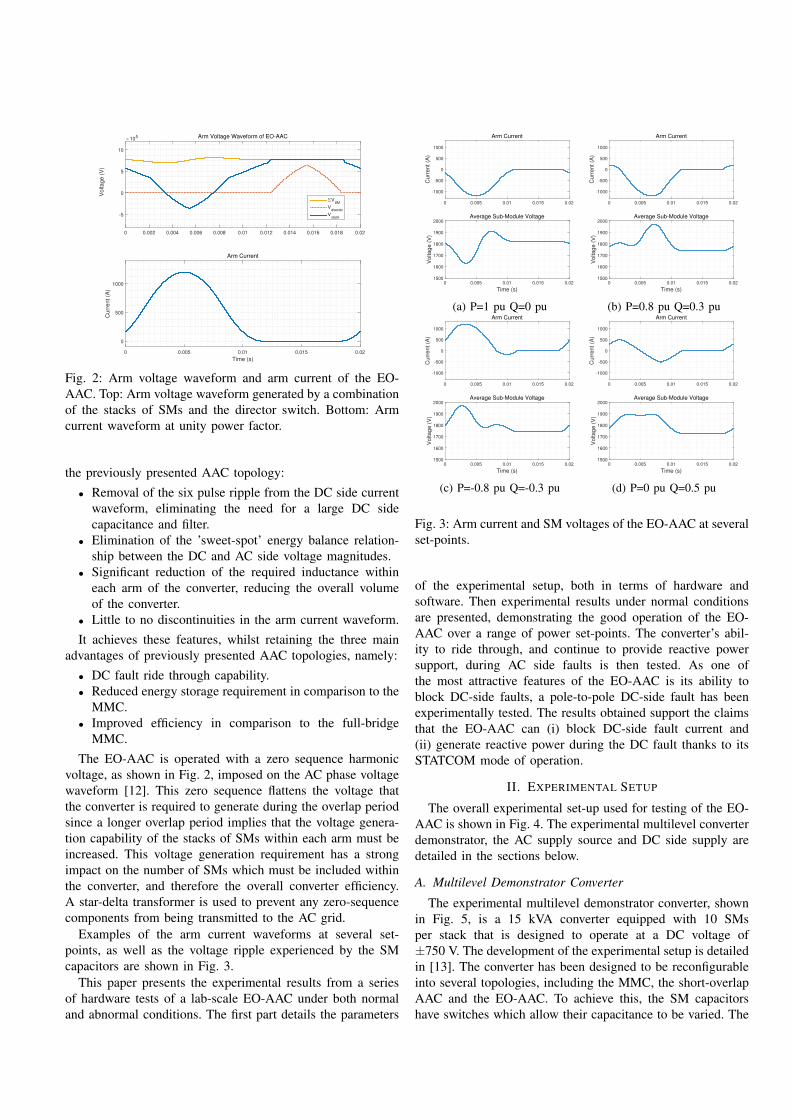
Fig. 2: Arm voltage waveform and arm current of the EO-
AAC. Top: Arm voltage waveform generated by a combination
of the stacks of SMs and the director switch. Bottom: Arm
current waveform at unity power factor.
the previously presented AAC topology:
• Removal of the six pulse ripple from the DC side current
waveform, eliminating the need for a large DC side
capacitance and filter.
• Elimination of the ’sweet-spot’ energy balance relation-
ship between the DC and AC side voltage magnitudes.
• Significant reduction of the required inductance within
each arm of the converter, reducing the overall volume
of the converter.
• Little to no discontinuities in the arm current waveform.
It achieves these features, whilst retaining the three main
advantages of previously presented AAC topologies, namely:
• DC fault ride through capability.
• Reduced energy storage requirement in comparison to the
MMC.
• Improved efficiency in comparison to the full-bridge
MMC.
The EO-AAC is operated with a zero sequence harmonic
voltage, as shown in Fig. 2, imposed on the AC phase voltage
waveform [12]. This zero sequence flattens the voltage that
the converter is required to generate during the overlap period
since a longer overlap period implies that the voltage genera-
tion capability of the stacks of SMs within each arm must be
increased. This voltage generation requirement has a strong
impact on the number of SMs which must be included within
the converter, and therefore the overall converter efficiency.
A star-delta transformer is used to prevent any zero-sequence
components from being transmitted to the AC grid.
Examples of the arm current waveforms at several set-
points, as well as the voltage ripple experienced by the SM
capacitors are shown in Fig. 3.
This paper presents the experimental results from a series
of hardware tests of a lab-scale EO-AAC under both normal
and abnormal conditions. The first part details the parameters
0 0.005 0.01 0.015 0.02
Curr
ent (A
)
-1000
-500
0
500
1000
Arm Current
Time (s)
0 0.005 0.01 0.015 0.02
Voltage (
V)
1500
1600
1700
1800
1900
2000Average Sub-Module Voltage
(a) P=1 pu Q=0 pu
0 0.005 0.01 0.015 0.02
Curr
ent (A
)
-1000
-500
0
500
1000
Arm Current
Time (s)
0 0.005 0.01 0.015 0.02
Voltage (
V)
1500
1600
1700
1800
1900
2000Average Sub-Module Voltage
(b) P=0.8 pu Q=0.3 pu
0 0.005 0.01 0.015 0.02
Curr
ent (A
)
-1000
-500
0
500
1000
Arm Current
Time (s)
0 0.005 0.01 0.015 0.02
Voltage (
V)
1500
1600
1700
1800
1900
2000Average Sub-Module Voltage
(c) P=-0.8 pu Q=-0.3 pu
0 0.005 0.01 0.015 0.02
Curr
ent (A
)
-1000
-500
0
500
1000
Arm Current
Time (s)
0 0.005 0.01 0.015 0.02
Voltage (
V)
1500
1600
1700
1800
1900
2000Average Sub-Module Voltage
(d) P=0 pu Q=0.5 pu
Fig. 3: Arm current and SM voltages of the EO-AAC at several
set-points.
of the experimental setup, both in terms of hardware and
software. Then experimental results under normal conditions
are presented, demonstrating the good operation of the EO-
AAC over a range of power set-points. The converter’s abil-
ity to ride through, and continue to provide reactive power
support, during AC side faults is then tested. As one of
the most attractive features of the EO-AAC is its ability to
block DC-side faults, a pole-to-pole DC-side fault has been
experimentally tested. The results obtained support the claims
that the EO-AAC can (i) block DC-side fault current and
(ii) generate reactive power during the DC fault thanks to its
STATCOM mode of operation.
II. EXPERIMENTAL SETUP
The overall experimental set-up used for testing of the EO-
AAC is shown in Fig. 4. The experimental multilevel converter
demonstrator, the AC supply source and DC side supply are
detailed in the sections below.
A. Multilevel Demonstrator Converter
The experimental multilevel demonstrator converter, shown
in Fig. 5, is a 15 kVA converter equipped with 10 SMs
per stack that is designed to operate at a DC voltage of
±750 V. The development of the experimental setup is detailed
in [13]. The converter has been designed to be reconfigurable
into several topologies, including the MMC, the short-overlap
AAC and the EO-AAC. To achieve this, the SM capacitors
have switches which allow their capacitance to be varied. The

Fig. 5: Experimental Setup. Left: Lab-Scale multilevel converter demonstrator with external power supplies. Top Right: SM
design with switchable SM capacitor. Bottom Right: Array of 60 SMs arranged into 6 stacks, director switch for operation as
AAC at the bottom of each stack.
Triphase 90kVA Back to back
Triphase 20kVA Bi-pole ±750V
Bipole
PSU
protection
DC
Fault
Lab-Scale Multilevel Demonstrator
Fig. 4: Experimental setup for testing of multilevel demonstra-
tor converter.
inductances within the circuit can also be quickly rearranged
to enable conversion between MMC and AAC operation. The
main characteristics of the converter, when operated as EO-
AAC, are summarised in Table I. The SM capacitors have been
sized in order to limit their voltage deviation to within ±10%,
leading to a total relative energy storage of 12.1 kJ/MVA which
is within the estimation provided in [14]. The converter is
controlled using an OPAL-RT real-time computing system.
B. DC System
The DC voltage source for the converter is provided by
a series pair of uni-directional 750V DC supplies that are
operated in parallel with a bi-pole arrangement of two 10
kVA two-level converters to form an overall bi-directional
DC supply. For DC fault testing the DC power supply and
TABLE I: Characteristics of the EO-AAC experiment
Characteristic Symbol Value
Power rating |S| 15 kVA
DC bus voltage VDC ±750 V
AC line voltage (RMS) Vline 1170 V
Nominal SM voltage VSM 110 V
Number of SMs per stack NSM 10
SM capacitor CSM 500 µF
Phase reactor L 24 mH
Arm inductor Larm 1.3 mH
DC inductor LDC 3.7 mH
DC bus capacitor CDC 210 µF
DC fault resistor Rfault 9.4 Ω
Control sampling frequency FS =1
TS10 kHz
two-level converters are protected using pairs of anti-parallel
thyristors.
C. AC system
The AC supply for the EO-AAC is provided by a bi-
directional 90 kVA two-level converter. As well as acting as
the AC supply, the two-level unit is used to synthesise three
phase and single line to ground faults.
D. DC Fault Setup
A DC-side fault emulator is used to generate faults on
the DC side. The DC fault emulator consists of two IGBTs,

each with a series fault resistor, that are connected between
the DC poles and earth. Since the objective is to ensure
that the experimental setup is representative of a full scale
system, the DC fault mechanism and the AAC are entirely
separate entities, and there is no communication between the
two systems.
The AAC controller must be able to detect the presence of a
fault in order to take the appropriate action. To achieve this, the
controller monitors the DC bus voltage for an under-voltage
event. When it occurs, the fault mode is activated, leading
to the drop of the active power reference to zero while the
reactive power reference is maintained at its pre-fault level.
After the DC bus voltage has collapsed, the active power
demand is periodically increased at a slow rate in an attempt
to determine if the fault is still present. If the DC current
rapidly increases, it is assumed that the fault is still present
and the active power demand is immediately dropped back to
zero until the next attempt. Once it has been determined that
the fault has been cleared, the DC bus capacitor voltage is
actively ramped up to its nominal value and the active power
reference is ramped back to its pre-fault value.
III. EXPERIMENTAL RESULTS
A. Normal Operation
The first test presented is the converter operating in steady-
state at 1 pu active power (inverting) and 0.5 pu reactive power
(capacitive). The results of this test are shown in Fig. 6a. The
DC voltages, DC current, stack voltage and arm current are
logged using current probes and differential voltage probes
connected to oscilloscopes. Other measurements are logged
by the OPAL-RT controller’s data acquisition system. The
converter exhibits good performance, capable of generating
low distortion AC side current waveforms. The DC current is
also free from six-pulse ripple, verifying the EO-AACs ability
to generate a smooth DC current without the need for a large
DC side filter. The SMs voltages are also stable around their
nominal set-point.
The stack voltage, sum SM voltages of each arm, and
director switch voltage of the upper arm of phase A over
one cycle are shown in the upper plot of Fig. 6b. The lower
plot shows the arm current overlaid with the phase current. It
can be seen that for part of the cycle, the arm is conducting
only the phase current. During the overlap periods, the arm is
conducting part of the phase currents as well as DC current.
When the director switch is open, the arm is not conducting
and the director switch and stack of SMs work together to
generate the necessary voltage.
The second steady-state test is a verification of the con-
verter’s ability to operate in STATCOM mode, generating
only reactive power. The converter was given a set-point of
0.7 pu reactive power (capacitive). The results are shown in
Fig. 7a. Again the converter exhibits good ability to generate
AC current waveforms with low distortion. The SMs are also
well controlled to their nominal value.
0 0.01 0.02 0.03 0.04 0.05 0.06 0.07 0.08
VA
C (
kV
)
-2
0
2
0 0.01 0.02 0.03 0.04 0.05 0.06 0.07 0.08
I A,B
,C (
A)
-10
0
10
0 0.01 0.02 0.03 0.04 0.05 0.06 0.07 0.08
VD
C (
kV
)
-1
0
1
0 0.01 0.02 0.03 0.04 0.05 0.06 0.07 0.08
I+ DC (
A)
-10
0
10
0 0.01 0.02 0.03 0.04 0.05 0.06 0.07 0.08
V+ A (
kV
)
-2
0
2
0 0.01 0.02 0.03 0.04 0.05 0.06 0.07 0.08
I+ A (
A)
-10
0
10
Time (s)
0 0.01 0.02 0.03 0.04 0.05 0.06 0.07 0.08
VS
M (
V)
50
100
150
200
(a) From Top: Converter AC line voltages, converterphase currents, DC pole to ground voltages, DC current,phase A upper arm stack voltage, phase A upper armcurrent, average SM voltage in each stack of SMs.
0 0.005 0.01 0.015 0.02
Vo
lta
ge
(kV
)
-1
-0.5
0
0.5
1
1.5
V+
AV
+
ADΣV
SM
Time (s)
0 0.005 0.01 0.015 0.02
Cu
rre
nt
(A)
-10
-5
0
5
10
I+
AIA
(b) One cycle of operation. Top: Phase A upper armstack voltage, director switch voltage and sum SMvoltage - Bottom: Phase A upper arm current and phasecurrent.
Fig. 6: Converter operating at a set-point of 1 pu P and 0.5
pu Q.

0 0.01 0.02 0.03 0.04 0.05 0.06 0.07 0.08
VA
C (
kV
)
-2
0
2
0 0.01 0.02 0.03 0.04 0.05 0.06 0.07 0.08
I A,B
,C (
A)
-10
0
10
0 0.01 0.02 0.03 0.04 0.05 0.06 0.07 0.08
VD
C (
kV
)
-1
0
1
0 0.01 0.02 0.03 0.04 0.05 0.06 0.07 0.08
I+ DC (
A)
-10
0
10
0 0.01 0.02 0.03 0.04 0.05 0.06 0.07 0.08
V+ A (
kV
)
-2
0
2
0 0.01 0.02 0.03 0.04 0.05 0.06 0.07 0.08
I+ A (
A)
-10
0
10
Time (s)
0 0.01 0.02 0.03 0.04 0.05 0.06 0.07 0.08
VS
M (
V)
50
100
150
200
(a) From Top: Converter AC line voltages, converterphase currents, DC pole to ground voltages, DC current,phase A upper arm stack voltage, phase A upper armcurrent, average SM voltage in each stack of SMs.
0 0.005 0.01 0.015 0.02
Vo
lta
ge
(kV
)
-1
-0.5
0
0.5
1
1.5
V+
AV
+
ADΣV
SM
Time (s)
0 0.005 0.01 0.015 0.02
Cu
rre
nt
(A)
-10
-5
0
5
10
I+
AIA
(b) One cycle of operation. Top: Phase A upper armstack voltage, director switch voltage and sum SMvoltage - Bottom: Phase A upper arm current and phasecurrent.
Fig. 7: Converter operating at a set-point of 0 pu P and 0.7
pu Q.
Fig. 7b shows a close up of the converter operation over
one cycle. Again it can be seen that the arm is conducting the
phase current for part of the cycle when the lower director
switch in the phase is open.
The last normal operation test of the converter is a power
reversal from -1 pu active power (rectifying) to 1 pu active
power (inverting). The converter’s reactive power set-point was
set to zero for this test. The converter’s slew rate on active
power was set to 10 pu/second, meaning it completed the full
power reversal in 200ms. The results of this test are shown in
Fig. 8.
During the power reversal a disturbance to the energy
levels within the SMs can be seen. The converter’s energy
management systems responds to this disturbance and restores
the SMs to their nominal voltage levels within 200 ms.
0 0.1 0.2 0.3 0.4 0.5 0.6
VA
C (
kV
)
-2
0
2
0 0.1 0.2 0.3 0.4 0.5 0.6
I A,B
,C (
A)
-10
0
10
0 0.1 0.2 0.3 0.4 0.5 0.6
VD
C (
kV
)
-1
0
1
0 0.1 0.2 0.3 0.4 0.5 0.6
I+ DC (
A)
-10
0
10
0 0.1 0.2 0.3 0.4 0.5 0.6
V+ A (
kV
)
-2
0
2
0 0.1 0.2 0.3 0.4 0.5 0.6
I+ A (
A)
-10
0
10
Time (s)
0 0.1 0.2 0.3 0.4 0.5 0.6
VS
M (
V)
50
100
150
200
Fig. 8: Power Reversal from -1 pu P to 1 pu P, converter is set
to 0 pu Q throughout. The format is the same as in Fig. 6a.
B. AC-Side Fault Operation
In this section the experimental results from two AC-side
fault tests are presented. A three-phase symmetrical fault and
a fault on one phase of the AC system was tested. The AC-
side faults were synthesised by the 90 kVA two-level converter
which acts as the grid source. In both fault cases, the voltage
on the faulted phases was reduced to 0.3 pu for 200 ms.
Upon detection of symmetrical faults, the converter is pro-
grammed to drop its pre-fault set-point and inject 1 pu reactive
current into the fault. For asymmetric faults the converter
is programmed to drop its pre-fault active power set-point

and inject 0.5 pu reactive current. After fault clearance the
converter is programmed to ramp back up to its pre-fault set-
point. Faults scenarios are detected using a sequence splitting
PLL.
The results of the symmetrical fault test are shown in Fig. 9.
The converter was commanded to a pre-fault set-point of -1
pu P (rectifying) and 0 pu Q.
At the fault inception, an over-voltage in the SMs within
the converter is seen, this is due to the sudden imbalance
between the AC and DC side powers. During the fault the
converter’s energy management system can be seen to be
bringing the SMs back towards their nominal value and
preventing any further divergence. After the fault clears the
converter resumes transferring active power. The energy levels
within the converter are returned to their nominal levels within
approximately 100 ms.
0 0.1 0.2 0.3 0.4 0.5 0.6
VA
C (
kV
)
-2
0
2
0 0.1 0.2 0.3 0.4 0.5 0.6
I A,B
,C (
A)
-10
0
10
0 0.1 0.2 0.3 0.4 0.5 0.6
VD
C (
kV
)
-1
0
1
0 0.1 0.2 0.3 0.4 0.5 0.6
I+ DC (
A)
-10
0
10
0 0.1 0.2 0.3 0.4 0.5 0.6
V+ A (
kV
)
-2
0
2
0 0.1 0.2 0.3 0.4 0.5 0.6
I+ A (
A)
-10
0
10
Time (s)
0 0.1 0.2 0.3 0.4 0.5 0.6
VS
M (
V)
50
100
150
200
Fig. 9: AC three phase symmetric Fault to 0.3 pu retained
voltage, pre-fault set-point is 1 pu P and 0 pu Q. The format
is the same as in Fig. 6a.
The results of the asymmetric fault test are shown in Fig. 10.
The converter’s pre-fault set-point was 1 pu active power
(inverting) and 0 pu reactive power.
The converter exhibits good ability to maintain operation
under the unbalanced grid conditions and successfully in-
jects reactive current into the fault. The SMs experience a
disturbance to their energy levels at the start of the fault,
however this is limited by the converter’s energy management
system. After the fault clears the converter resumes active
power transfer. As with the three phase fault, the converter’s
energy levels are returned to their nominal levels within
approximately 100 ms after the fault clearance.
0 0.1 0.2 0.3 0.4 0.5 0.6
VA
C (
kV
)
-2
0
2
0 0.1 0.2 0.3 0.4 0.5 0.6
I A,B
,C (
A)
-10
0
10
0 0.1 0.2 0.3 0.4 0.5 0.6
VD
C (
kV
)
-1
0
1
0 0.1 0.2 0.3 0.4 0.5 0.6
I+ DC (
A)
-10
0
10
0 0.1 0.2 0.3 0.4 0.5 0.6V
+ A (
kV
)-2
0
2
0 0.1 0.2 0.3 0.4 0.5 0.6
I+ A (
A)
-10
0
10
Time (s)
0 0.1 0.2 0.3 0.4 0.5 0.6
VS
M (
V)
50
100
150
200
Fig. 10: AC single line to ground asymmetric fault with 0.3
pu retained voltage on faulted phase, pre-fault set-point is -1
pu P and 0 pu Q. The format is the same as in Fig. 6a.
C. DC-Side Fault Operation
In this test, the AAC had to withstand a 200 ms fault on
the DC bus, which is applied using the system described in
Section II-D. Pre-fault the converter was set to -1 pu active
power (rectifying) and -0.5 pu reactive power (inductive). The
controller is set to retain the reactive power set-point through
the DC fault. The results of this test are shown in Fig. 11.
At the instance of the fault, the DC bus voltage rapidly
collapses with a large spike of the DC current from the DC bus
capacitor which reaches 68.5A. This peak current is shown off
the scale of the plot to show the finer details of the DC current
during the test. The DC bus under-voltage event is detected
by the control system and the converter does not contribute
to the DC side fault current. The converter maintains good
control over the AC side currents, quickly dropping its active
power and moving into STATCOM mode. The DC current
can be seen to go to zero after the DC bus capacitor has been
drained.
During the fault, the controller periodically attempts to
inject power into the DC bus. If this causes the DC voltage to
rise, indicating fault clearance, the converter is programmed
to re-energize the DC bus and resume its pre-fault set-point.

In this way, the converter acts in a similar manner to an auto
re-closing circuit breaker between the AC and DC systems.
After fault clearance the converter recharges the DC bus and
resumes active power flow. As the DC current is measured
outside the DC bus capacitor, no current is measured during
the recharging stage until the bus voltage become high enough
to forward bias the protection thyristors.
The converter exhibits good ability to maintain the energy
levels within the SMs during the DC fault. A slight disturbance
is seen at the start of the fault, however the energy management
system prevents the SMs from running away from their set-
point. After the fault clears, the SMs are returned to their
nominal voltage levels within approximately 100 ms.
0 0.1 0.2 0.3 0.4 0.5 0.6
VA
C (
kV
)
-2
0
2
0 0.1 0.2 0.3 0.4 0.5 0.6
I A,B
,C (
A)
-10
0
10
0 0.1 0.2 0.3 0.4 0.5 0.6
VD
C (
kV
)
-1
0
1
0 0.1 0.2 0.3 0.4 0.5 0.6
I+ DC (
A)
-10
0
10
0 0.1 0.2 0.3 0.4 0.5 0.6
V+ A (
kV
)
-2
0
2
0 0.1 0.2 0.3 0.4 0.5 0.6
I+ A (
A)
-10
0
10
Time (s)
0 0.1 0.2 0.3 0.4 0.5 0.6
VS
M (
V)
50
100
150
200
Fig. 11: DC pole to pole fault with a 9.4 Ω fault impedance.
Pre-fault set-point is -1 pu P and -0.5 pu Q. The format is the
same as in Fig. 6a.
IV. CONCLUSION
The Alternate Arm Converter (AAC) is a hybrid multilevel
converter with DC-side fault blocking capability and a re-
duced number of SMs. Its new Extended Overlap (EO) mode
shows significant improvements over previous iterations of
the design, notably the removal of the six-pulse ripple in the
DC current waveform and the elimination of the ’sweet-spot’
energy relationship between the DC and AC side voltages. This
paper presents the first experimental results of an EO-AAC
operating across a range of steady-state and fault scenarios.
Tests with a 15 kVA EO-AAC showed the ability of this
hybrid topology to provide a range of active and reactive
powers, as well as to successfully ride through AC side fault
scenarios. Importantly, the DC-side fault blocking capability of
the EO-AAC has been demonstrated by showing (i) its ability
to keep complete control of the AC currents during a DC-side
fault, (ii) its STATCOM mode of operation and (iii) the rapid
reestablishment of the DC bus voltage and normal power flow
after fault clearance. The availability of DC-fault blocking in
a multilevel converter with an efficiency broadly similar to a
half-bridge MMC makes the EO-AAC an interesting choice
for VSC HVDC.
ACKNOWLEDGMENT
The authors gratefully acknowledge the financial support
provided by Hubnet Consortium (EPSRC grant EP/I013636/1),
the UK Power Electronic Centre: Converter Theme (ESPRC
grant EP/K035096/1), the Top and Tail consortium (EPSRC
grant EP/I031707/1), EDF Energy R&D UK and the cooper-
ation of Alstom Grid, including the use of control algorithms
for these tests which were developed on their behalf.
REFERENCES
[1] D. Trainer et al., “A new hybrid voltage-sourced converter for HVDCpower transmission,” in Cigre Session, 2010.
[2] M. Merlin et al., “The alternate arm converter: A new hybrid multilevelconverter with DC-fault blocking capability,” Power Delivery, IEEE
Transactions on, vol. 29, no. 1, pp. 310–317, Feb. 2014.[3] A. Nami et al., “Modular multilevel converters for HVDC applications:
Review on converter cells and functionalities,” Power Electronics, IEEE
Transactions on, vol. 30, no. 1, pp. 18–36, Jan. 2015.[4] M. Perez et al., “Circuit topologies, modeling, control schemes, and
applications of modular multilevel converters,” Power Electronics, IEEE
Transactions on, vol. 30, no. 1, pp. 4–17, Jan. 2015.[5] A. Lesnicar and R. Marquardt, “An innovative modular multilevel
converter topology suitable for a wide power range,” in Power Tech
Conference Proceedings, 2003 IEEE Bologna, vol. 3, Jun. 2003.[6] M. Merlin and T. Green, “Cell capacitor sizing in multilevel converters:
Cases of the MMC and AAC,” IET Power Electronics, 2014.[7] R. Feldman et al., “DC fault ride-through capability and statcom opera-
tion of a hybrid voltage source converter arrangement for HVDC powertransmission and reactive power compensation,” in Power Electronics,
Machines and Drives (PEMD 2012), 6th IET International Conference
on, Mar. 2012, pp. 1–5.[8] R. Feldman et al., “DC fault ride-through capability and STATCOM
operation of a HVDC hybrid voltage source converter,” IET Generation,
Transmission & Distribution, vol. 8, no. 1, pp. 114–120, 2014.[9] J. Ainsworth et al., “Static VAr compensator (STATCOM) based on
single-phase chain circuit converters,” Generation, Transmission and
Distribution, IEE Proceedings-, vol. 145, no. 4, pp. 381 –386, Jul. 1998.[10] S. Fekriasl et al., “Improvements in or relating to the control
of converters,” Patent EP2 884 653, June, 2015. [Online]. Available:http://www.freepatentsonline.com/EP2884653A1.html
[11] D. Trainer et al., “Converter,” May 7 2014, eP Patent App.EP20,110,728,832. [Online]. Available: https://www.google.com.ar/patents/EP2727234A1?cl=en
[12] F. Moreno et al., “Zero phase sequence voltage injection for the alternatearm converter,” in AC and DC Power Transmission, 2015. ACDC. 10th
IET International Conference on, Feb. 2015.[13] P. Clemow et al., “Lab-scale experimental multilevel modular HVDC
converter with temperature controlled cells,” in Power Electronics and
Applications (EPE’14-ECCE Europe), 2014 16th European Conference
on, Aug. 2014, pp. 1–10.[14] M. Merlin et al., “Cell capacitor sizing in modular multilevel converters
and hybrid topologies,” in Power Electronics and Applications (EPE’14-
ECCE Europe), 2014 16th European Conference on, Aug. 2014, pp.1–10.