Lan and Wan Technologies Networking Internet Working Hardware 4689
Hardware Technologies for RobustPersonal Communication Transceivers
Integrated Circuits & Systems LaboratoryElectrical Engineering DepartmentUniversity of CaliforniaLos Angeles, CA 90024-1594
Henry SamueliAsad A. Abidi
Gregory J. PottieYahya Rahmat-Samii

UCLA Low-Power Transceiver Program
∑ Low-Voltage Custom Analog & Digital CMOS∑ Monolithic CMOS 915 MHz Receive/Transmit Path∑ Two-chip Design; Minimum Discrete Components
Low Power Dissipation
Up to 160 kb/s ∑ Space Diversity with Multiple Antennas∑ Frequency Diversity with Spread-Spectrum∑ Time Diversity with ECC/Interleaving
Robustness
Means: Investigate analog, digital, and antennatechnologies, coupled tightly to system design
Objective: Low-power, handheld, robust transceivers forindoor and mobile personal communications
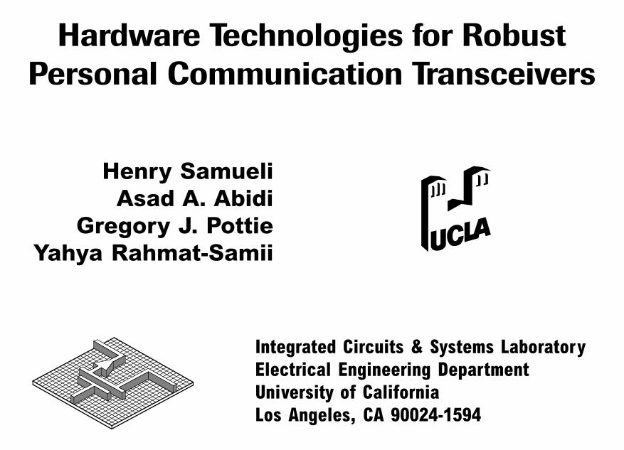
The UCLA Frequency-HoppedSpread-Spectrum CMOS Transceiver
Digital AnalogFSKDetector
BPF
BPF
Frequency Control Logic
DDFS
DDFS
915 MHzLocal Oscillator
SSB Select
Freq
uenc
y & T
imin
g Ac
quis
itio
n
Base
band
Dat
a Ou
t
Baseband Data In
10b
10b
PA
Power Control
LNA
LPF
LPF
LPF
LPF
90˚
LNA90˚
Limiter
Limiter
Limiter
Limiter

Performance Specifications of Handset
Power Dissipation of Handset
225 mW in receive, 300 mW in transmit
F
r
e
q
u
e
n
c
y
B
a
n
d
902-928 MHz (unlicensed ISM band)
Radiated Power
20 mW (max); 20 µW (min)
D
a
t
a
R
a
t
e
2 to 160 kb/s (variable)
Duplexing
T
i
m
e
D
i
v
i
s
i
o
n
D
u
p
l
e
x
b
e
t
w
e
e
n
T
X
a
n
d
R
X
Multiple Access Method
F
r
e
q
u
e
n
c
y
-
H
o
p
p
e
d
S
p
r
e
a
d
-
S
p
e
c
t
r
u
m
C
D
M
A
Coding
R
a
t
e
-
½
C
o
n
v
o
l
u
t
i
o
n
a
l
C
o
d
e
(
k
=
6
)
Modulation
B
i
n
a
r
y
o
r
Q
u
a
t
e
r
n
a
r
y
F
S
K
P
o
w
e
r
S
u
p
p
l
y
3 V (max)
IC Technology
1-µm bulk CMOS
Receive Antennas
M
u
l
t
i
p
l
e
m
i
n
i
a
t
u
r
e
e
m
b
e
d
d
e
d
e
l
e
m
e
n
t
s
w
i
t
h
s
p
a
c
e
a
n
d
p
o
l
a
r
i
z
a
t
i
o
n
d
i
v
e
r
s
i
t
y
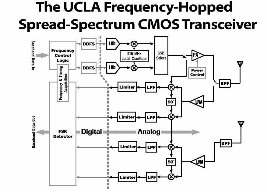
Spread-Spectrum Systems:Hardware Implications
n Frequency Diversity by making chip-rate >> symbol rate
n Equalization at chip-rate High-speed signal processing required
n Coherent receiver most common
n Main advantage: SNR gain withcoherent detection, optimummodulation
n Limitation: High complexity
n Covers wide bandwidth with lowhop-rate
n Equalization at hop-rate only
n Simple binary FSK modulation maybe used
n Non-coherent receiver is simple
n Main advantage: Low-power receiver
n Limitation: Sub-optimal channelcapacity
Direct Sequence Frequency Hopped
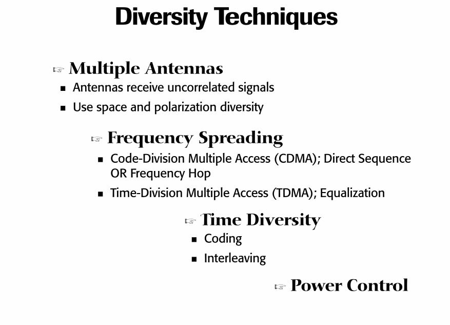
Diversity Techniques
n Antennas receive uncorrelated signals
n Use space and polarization diversity
n Code-Division Multiple Access (CDMA); Direct SequenceOR Frequency Hop
n Time-Division Multiple Access (TDMA); Equalization
n Coding
n Interleaving
e Power Control
e Multiple Antennas
e Time Diversity
e Frequency Spreading
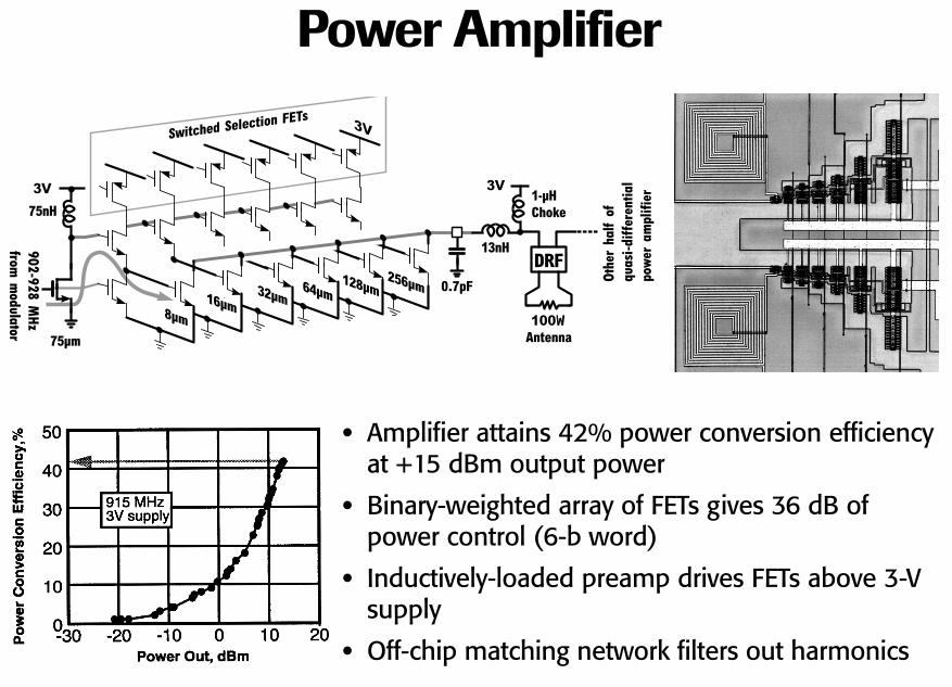
Power Amplifier
• Amplifier attains 42% power conversion efficiencyat +15 dBm output power
• Binary-weighted array of FETs gives 36 dB ofpower control (6-b word)
• Inductively-loaded preamp drives FETs above 3-Vsupply
• Off-chip matching network filters out harmonics
Switched Selection FETs
DRF
100WAntenna
0.7pF
13nH
75nH
75µm
8µm16µm
32µm
256µm64µm128µm
3V3V
3V
1-µHChoke
Othe
r ha
lf o
fqu
asi-
diff
eren
tial
pow
er a
mpl
ifier
902-928 MH
zfrom
modulator

Frequency-Hopped Synthesizer
• DDFS produces samples of a sinewave at a frequency selected by 11-b word;instantly agile frequency source
• DDFS output range is 013 MHz; adding up-converted outputs produces SSB915928 MHz; subtracting them produces 902915 MHz
• 8-b matching required between channels for adequate image suppression
Phas
e Ac
cum
ulat
or (11
b) SINE ROM
COSINE ROM
10b DAC
Direct Digital Frequency Synthesizer
I
915 MHz Local Osc
I
Q
Q
10b DAC
Sign Select Control
Anti-alias Filter
Circuits implemented on this prototype
Freq
uenc
y Co
ntro
l W
ord
(11b
)
F/H
S/S
SSB
Anti-alias Filter
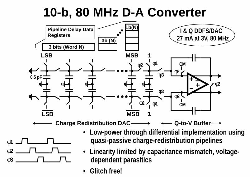
10-b, 80 MHz D-A Converter
LSB
LSB
3 bits (Word N)3b (N)
1b(N)
MSB
MSB
Pipeline Delay DataRegisters
1
1
φ2
φ2 φ1
φ1
φ2
φ2
φ2
φ3
φ3
++
CM
CM
0.5 pF
Charge Redistribution DAC Q-to-V Buffer
I & Q DDFS/DAC27 mA at 3V, 80 MHz
• Low-power through differential implementation usingquasi-passive charge-redistribution pipelines
• Linearity limited by capacitance mismatch, voltage-dependent parasitics
• Glitch free!
φ1
φ2
φ3

Measured DDFS/DAC Spectral Outputs
62 dB
50 MHz Sample Rate3 V Supply
0 5 MHz 0 25 MHz
50 MHz Sample Rate3 V Supply
16.715 MHz
57 dB
–57 dBc
•
•
•
• Spurious level as predicted• set by capacitor mismatch
• Inter-cell capacitance causesnon-linearity at high frequency
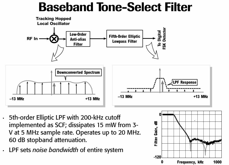
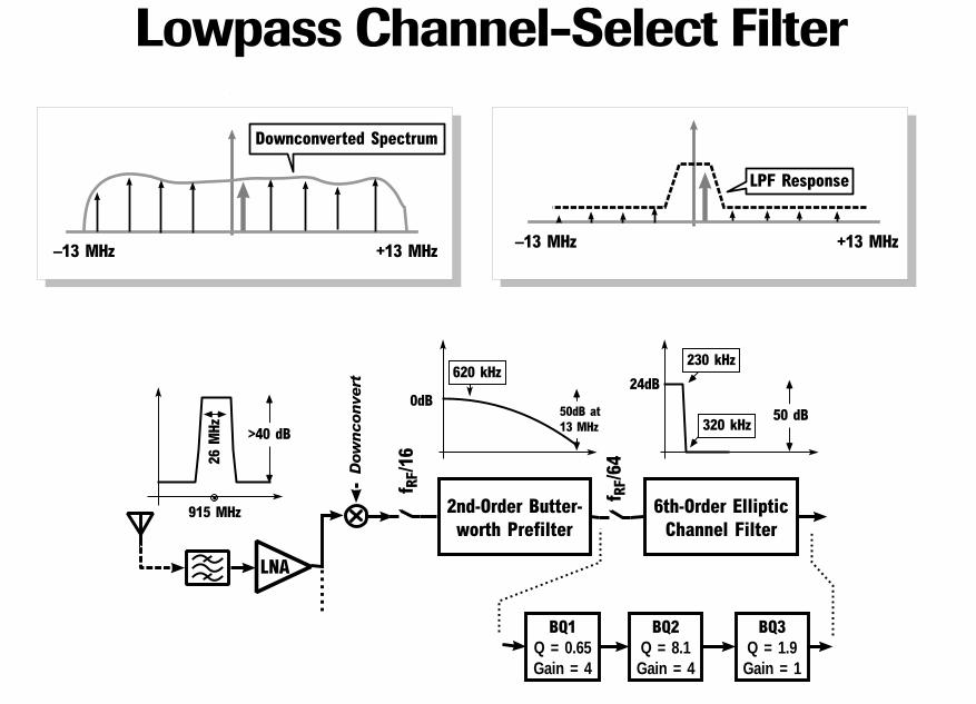
Baseband Tone-Select Filter
Low-Order Anti-alias
Filter
Fifth-Order Elliptic Lowpass Filter
To D
igita
l FS
K D
etec
tor
RF In
Tracking Hopped Local Oscillator
+13 MHz
LPF Response
–13 MHz+13 MHz
Downconverted Spectrum
–13 MHz
0 1000Frequency, kHz
0
-120
• 5th-order Elliptic LPF with 200-kHz cutoffimplemented as SCF; dissipates 15 mW from 3-V at 5 MHz sample rate. Operates up to 20 MHz.60 dB stopband attenuation.
• LPF sets noise bandwidth of entire system
50dB at13 MHz>40 dB
50 dB
LNA
Dow
nconve
rt
2nd-Order Butter-worth Prefilter
BQ1Q = 0.65Gain = 4
BQ2Q = 8.1
Gain = 4
BQ3Q = 1.9
Gain = 1
6th-Order Elliptic Channel Filter
f RF/16
f RF/64
620 kHz230 kHz
320 kHz
24dB
26 M
Hz
915 MHz
0dB
Lowpass Channel-Select Filter
+13 MHz
LPF Response
–13 MHz+13 MHz
Downconverted Spectrum
–13 MHz

Measured Filter Performance
· 70 nV/Hz in passband
· 4.6 mA from 3V
· 200 pF total on-chipcapacitance

Digital Tone Detector
I&D
I&D
I&D
I&D
|A|+|B|
|A|+|B|
|A|+|B|
|A|+|B|
Max Select
MUX9b
MSBcoswt
(1b)
sinwt
(1b)
• 1-bit oversampled correlator (programmable oversample rate)
• Multipliers are switches, integrators are accumulators
• 1.9 sq mm active area implementation will dissipate 2 mW
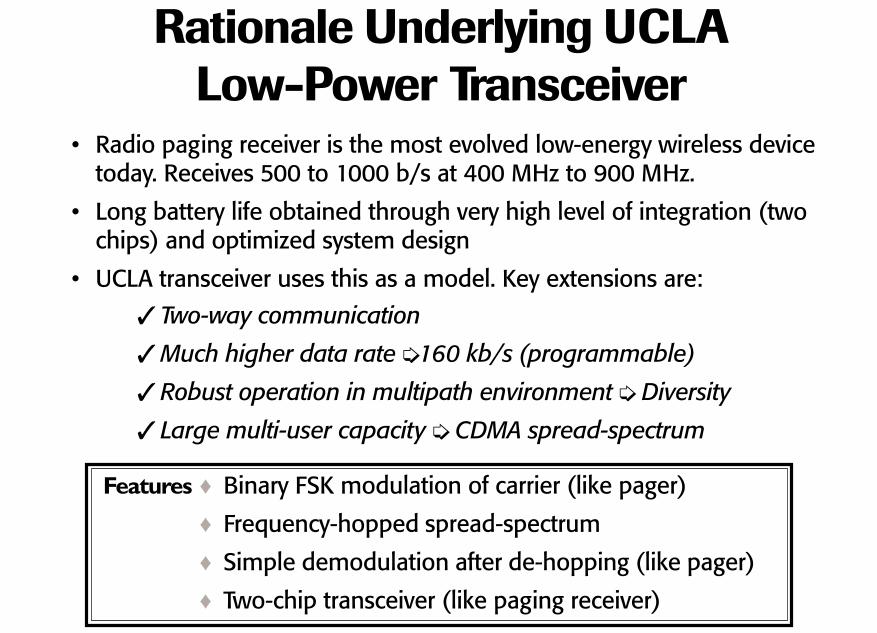
Rationale Underlying UCLALow-Power Transceiver
• Radio paging receiver is the most evolved low-energy wireless devicetoday. Receives 500 to 1000 b/s at 400 MHz to 900 MHz.
• Long battery life obtained through very high level of integration (twochips) and optimized system design
• UCLA transceiver uses this as a model. Key extensions are:
♦ Binary FSK modulation of carrier (like pager)
♦ Frequency-hopped spread-spectrum
♦ Simple demodulation after de-hopping (like pager)
♦ Two-chip transceiver (like paging receiver)
Two-way communication
Much higher data rate 160 kb/s (programmable)
Robust operation in multipath environment Diversity
Large multi-user capacity CDMA spread-spectrum
Features
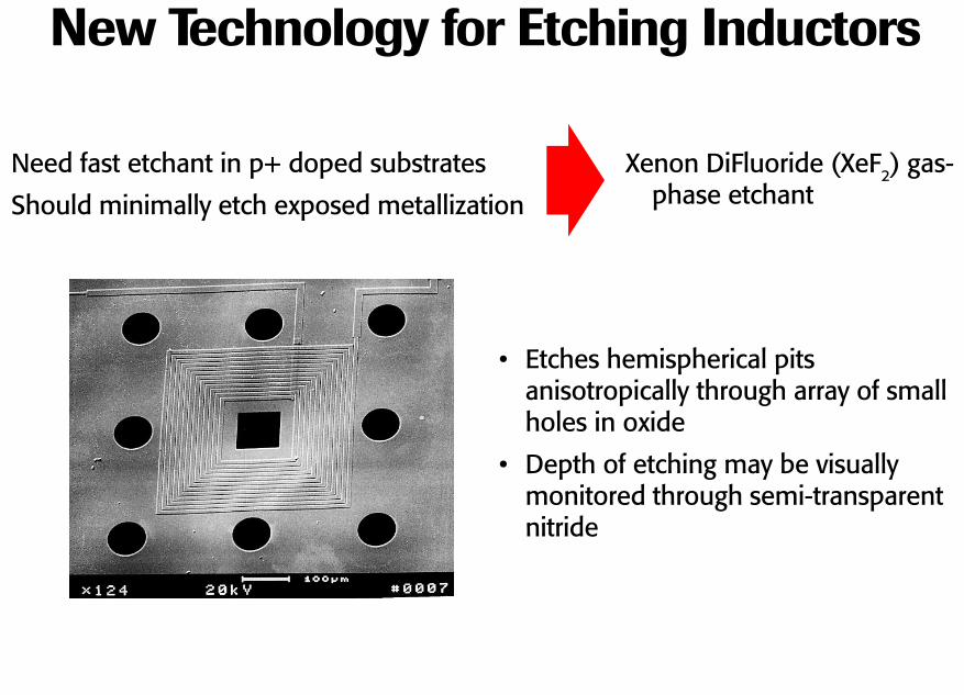
New Technology for Etching Inductors
Need fast etchant in p+ doped substrates
Should minimally etch exposed metallization
Xenon DiFluoride (XeF2) gas-phase etchant
• Etches hemispherical pitsanisotropically through array of smallholes in oxide
• Depth of etching may be visuallymonitored through semi-transparentnitride
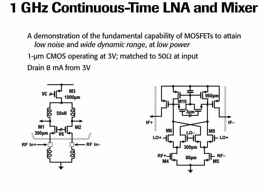
1 GHz Continuous-Time LNA and Mixer
A demonstration of the fundamental capability of MOSFETs to attainlow noise and wide dynamic range, at low power
1-µm CMOS operating at 3V; matched to 50W at input
Drain 8 mA from 3V
50nH
VG
VC
RF In+ RF In–
M31000µm
M1300µm
M2
M480µm
3µm
M10
M6 M9
960µm
300µm
M5RF+
LO+
IF+ IF–
LO+LO–
RF–
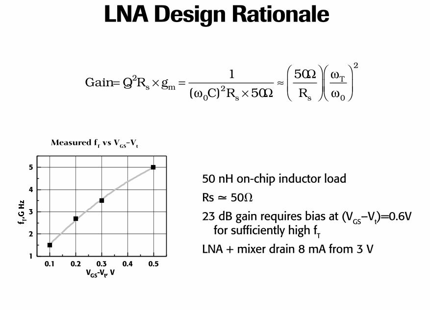
LNA Design Rationale
Gain Q R gC R R
s ms s
T= ¥ =¥
ªFHG
IKJFHG
IKJ
2
02
0
21
50
50
( )wwwW
W
0.1 0.2 0.3 0.4 0.51
2
3
4
5
VGS-Vt, V
50 nH on-chip inductor load
Rs ..... 50V
23 dB gain requires bias at (VGS–Vt)=0.6Vfor sufficiently high fT
LNA + mixer drain 8 mA from 3 V
Measured fT vs VGS-Vt
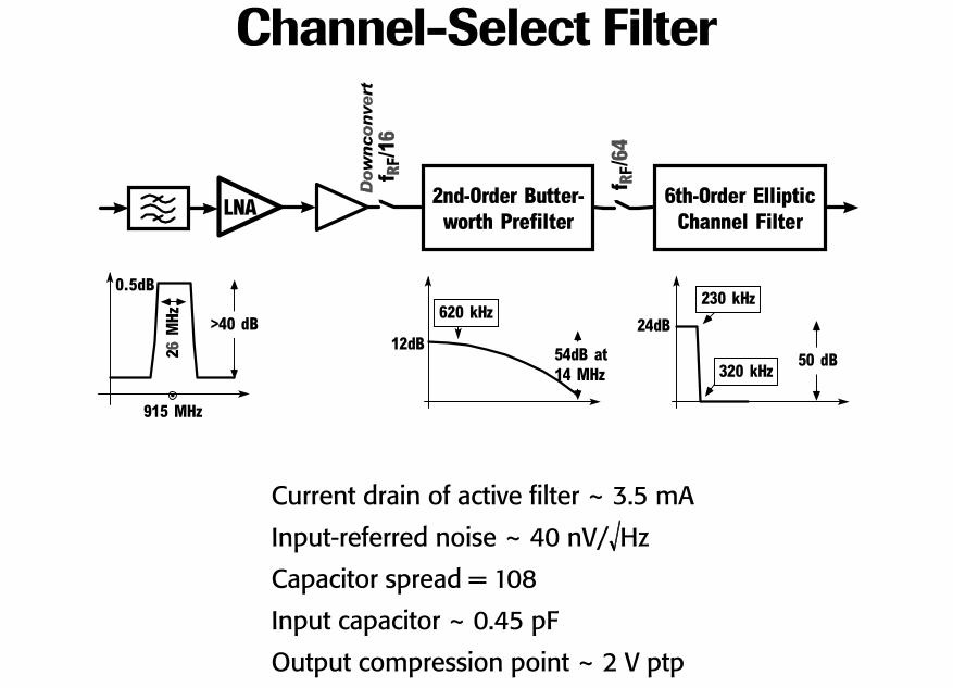
Channel-Select Filter
Current drain of active filter ~ 3.5 mA
Input-referred noise ~ 40 nV/!!!!!Hz
Capacitor spread = 108
Input capacitor ~ 0.45 pF
Output compression point ~ 2 V ptp
54dB at14 MHz
>40 dB
50 dB
LNA 2nd-Order Butter-worth Prefilter
6th-Order Elliptic Channel Filter
620 kHz230 kHz
320 kHz
24dB
0.5dB
915 MHz
12dB
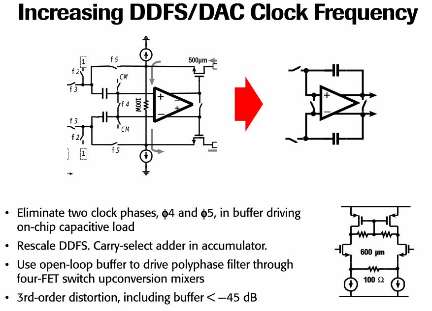
Increasing DDFS/DAC Clock Frequency
• Eliminate two clock phases, fffff4 and fffff5, in buffer drivingon-chip capacitive load
• Rescale DDFS. Carry-select adder in accumulator.
• Use open-loop buffer to drive polyphase filter throughfour-FET switch upconversion mixers
• 3rd-order distortion, including buffer < —45 dB
600 µm
100 WW
–+100
Ω
Ω
(
f5
f5
f2f2
f2
f3
f3
CM
CM
f4
500µm
–+
1
1
–+
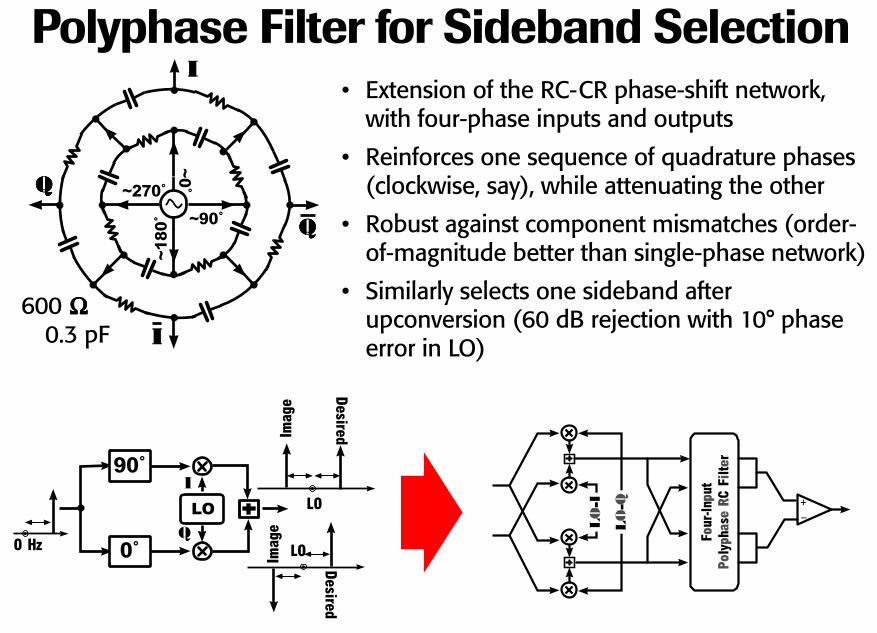
Polyphase Filter for Sideband Selection
LO
I
Q0˚
90˚
DesiredDesired
Imag
eIm
age
LO
O Hz LO
–+
IIIII
IIIII
QQQQQ
QQQQQ
~0˚
~180˚
~270˚
~90˚
600 WWWWW0.3 pF
• Extension of the RC-CR phase-shift network,with four-phase inputs and outputs
• Reinforces one sequence of quadrature phases(clockwise, say), while attenuating the other
• Robust against component mismatches (order-of-magnitude better than single-phase network)
• Similarly selects one sideband afterupconversion (60 dB rejection with 10° phaseerror in LO)

Transmitter Test Chip6×3.8 mm active area
65 mA active current
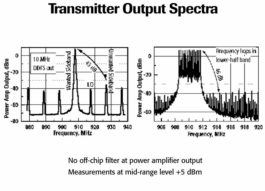
Transmitter Output Spectra
No off-chip filter at power amplifier output
Measurements at mid-range level +5 dBm
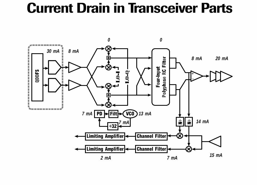
Current Drain in Transceiver Parts
30 mA 8 mA8 mA
14 mA
15 mA7 mA
7 mA
7 mA
2 mA
13 mA
20 mA
0 0
Filt VCO
–+
÷32
PD
Channel Filter
Channel Filter
Limiting Amplifier
Limiting Amplifier
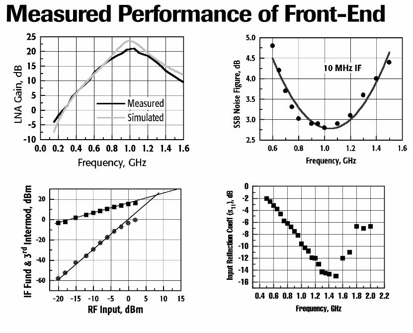
Measured Performance of Front-End
0.4 0.6 0.8 1.0 1.2 1.4 1.6 1.8 2.0 2.2
-16-14-12-10
-8-6-4-20
Frequency, GHz