
HALT Testing of Backward Soldered BGAs on a Military … · Figure 2 – Circuit card test vehicle...
11
HALT Testing of Backward Soldered BGAs on a Military Product B. Gumpert, B. Fox, L. Woody Lockheed Martin Ocala, FL Abstract The move to lead free (Pb-free) electronics by the commercial industry has resulted in an increasing number of ball grid array components (BGAs) which are only available with Pb-free solder balls. The reliability of these devices is not well established when assembled using a standard tin-lead (SnPb) solder paste and reflow profile, known as a backward compatible process. Previous studies in processing mixed alloy solder joints have demonstrated the importance of using a reflow temperature high enough to achieve complete mixing of the SnPb solder paste with the Pb-free solder ball. Research has indicated that complete mixing can occur below the melting point of the Pb-free alloy and is dependent on a number of factors including solder ball composition, solder ball to solder paste ratio, and peak reflow times and temperatures. Increasing the lead content in the system enables full mixing of the solder joint with a reduced peak reflow temperature, however, previous research is conflicting regarding the effect that lead percentage has on solder joint reliability in this mixed alloy solder joint. Previous work by the authors established a protocol for soldering Pb-free BGAs with SnPb solder paste based on solder ball size and target lead content in the final solder joint. The units from that testing were subjected to thermal cycling between -55°C and 125°C and compared to a SnPb baseline assembly. Results showed that mixed alloy joints performed as well as or better than standard SnPb joints under these conditions. This study continues the previous work with evaluation of reliability in a production design. Functional assemblies were built using Pb-free BGAs in a SnPb solder process and subjected to life testing including accelerated aging and highly accelerated life testing (HALT). Results from this testing are compared to SnPb baseline units and previous product development test results. Introduction Europe’s Restriction of Hazardous Substances (RoHS) and similar lead -free directives from nations outside the European Union have caused the electronics industry to move towards lead-free soldering. Some manufacturers building high-reliability electronics and/or products with a long service life which are outside of the scope of these directives continue to use conventional tin-lead (SnPb) solder due to the uncertain reliability of lead-free solder joints. Because component manufacturers are moving to lead-free production, many components are no longer available in SnPb. As availability of SnPb BGAs and chip scale packages (CSPs) continues to diminish, fabricators who continue to use a SnPb process will be compelled to accommodate lead-free versions of these packages by either reballing the package, or using them as-is in a backward compatible process. Reballing is currently an acceptable process for many, but carries with it the disadvantages of potential damage to the package, voiding of the component manufacturer’s warranty, and/or significant cost impacts. Soldering of lead-free components with SnPb solder, called backward compatibility, has therefore become an area of particular interest. The mixing of metallurgies can induce new reliability concerns because solder joint reliability depends on loading conditions, material properties and microstructure of the solder joint. Furthermore, the microstructure of the solder joint continues to evolve over time depending on temperature and mechanical loading conditions. One of the microstructural features known to influence the reliability of conventional SnPb solder is the lead (Pb) phase, which coarsens with time, temperature and mechanical loading, causing reliability concerns [1][2]. It is therefore important to understand any impact to reliability resulting from the mixing of solder alloys, particularly in the use of components which have a volume of lead-free solder that is significant to the final solder volume in the joint, such as BGAs and CSPs. Numerous studies have been conducted to investigate the reliability of the mixed solder joints subjected to various loading conditions and metallurgical combinations. In general, results from these studies indicate that for lead-free As originally published in the IPC APEX EXPO Conference Proceedings.
-
Upload
trinhduong -
Category
Documents
-
view
218 -
download
2
Transcript of HALT Testing of Backward Soldered BGAs on a Military … · Figure 2 – Circuit card test vehicle...

HALT Testing of Backward Soldered BGAs on a Military Product
B. Gumpert, B. Fox, L. Woody
Lockheed Martin
Ocala, FL
Abstract The move to lead free (Pb-free) electronics by the commercial industry has resulted in an increasing number of ball
grid array components (BGAs) which are only available with Pb-free solder balls. The reliability of these devices is
not well established when assembled using a standard tin-lead (SnPb) solder paste and reflow profile, known as a
backward compatible process. Previous studies in processing mixed alloy solder joints have demonstrated the
importance of using a reflow temperature high enough to achieve complete mixing of the SnPb solder paste with the
Pb-free solder ball. Research has indicated that complete mixing can occur below the melting point of the Pb-free
alloy and is dependent on a number of factors including solder ball composition, solder ball to solder paste ratio, and
peak reflow times and temperatures. Increasing the lead content in the system enables full mixing of the solder joint
with a reduced peak reflow temperature, however, previous research is conflicting regarding the effect that lead
percentage has on solder joint reliability in this mixed alloy solder joint.
Previous work by the authors established a protocol for soldering Pb-free BGAs with SnPb solder paste based on
solder ball size and target lead content in the final solder joint. The units from that testing were subjected to thermal
cycling between -55°C and 125°C and compared to a SnPb baseline assembly. Results showed that mixed alloy
joints performed as well as or better than standard SnPb joints under these conditions.
This study continues the previous work with evaluation of reliability in a production design. Functional assemblies
were built using Pb-free BGAs in a SnPb solder process and subjected to life testing including accelerated aging and
highly accelerated life testing (HALT). Results from this testing are compared to SnPb baseline units and previous
product development test results.
Introduction
Europe’s Restriction of Hazardous Substances (RoHS) and similar lead-free directives from nations outside the
European Union have caused the electronics industry to move towards lead-free soldering. Some manufacturers
building high-reliability electronics and/or products with a long service life which are outside of the scope of these
directives continue to use conventional tin-lead (SnPb) solder due to the uncertain reliability of lead-free solder
joints. Because component manufacturers are moving to lead-free production, many components are no longer
available in SnPb.
As availability of SnPb BGAs and chip scale packages (CSPs) continues to diminish, fabricators who continue to
use a SnPb process will be compelled to accommodate lead-free versions of these packages by either reballing the
package, or using them as-is in a backward compatible process. Reballing is currently an acceptable process for
many, but carries with it the disadvantages of potential damage to the package, voiding of the component
manufacturer’s warranty, and/or significant cost impacts. Soldering of lead-free components with SnPb solder,
called backward compatibility, has therefore become an area of particular interest.
The mixing of metallurgies can induce new reliability concerns because solder joint reliability depends on loading
conditions, material properties and microstructure of the solder joint. Furthermore, the microstructure of the solder
joint continues to evolve over time depending on temperature and mechanical loading conditions. One of the
microstructural features known to influence the reliability of conventional SnPb solder is the lead (Pb) phase, which
coarsens with time, temperature and mechanical loading, causing reliability concerns [1][2]. It is therefore
important to understand any impact to reliability resulting from the mixing of solder alloys, particularly in the use of
components which have a volume of lead-free solder that is significant to the final solder volume in the joint, such
as BGAs and CSPs.
Numerous studies have been conducted to investigate the reliability of the mixed solder joints subjected to various
loading conditions and metallurgical combinations. In general, results from these studies indicate that for lead-free
As originally published in the IPC APEX EXPO Conference Proceedings.

BGA components assembled with lead-based solder, the reliability is equivalent to completely lead-free assemblies,
provided that the Pb is distributed evenly throughout the joint [3-9]. Correspondingly, several studies found that the
reliability of solder interconnections degraded when a SAC solder ball is only partially mixed with SnPb solder
paste [4][6][10].
The degree of mixing in backward compatibility assembly is expected to be a function of the reflow peak
temperature, time above liquidus (183°C), the alloys used (ball and paste), and the mix ratio of those
alloys[3][7][11-18]. In previous studies, the authors developed processing guidelines for lead-free BGAs and CSPs
with SnPb solder paste based on lead content, reflow peak temperature, and time above liquidus (TAL)[19]. The
result was the chart shown in Figure 1, which is used by the assembler to ensure that full alloy mixing in the BGA
solder joint is achieved, thus providing a reliable joint, while allowing the assembler to adjust the desired parameters
of their process to optimize for design-specific restrictions.
Figure 1 - Pb content (% wt.) curves for predicting full mixing of
backward compatible solder joints based on TP and TAL (183°C)
In this study, the guidelines developed in that previous work were used to fabricate hardware of an existing
production design where the SnPb-balled BGAs are replaced with components which have SAC305 balls. This
hardware was then be subjected to HALT and accelerated aging in a fashion similar to the tests used to validate
other design changes, to demonstrate the reliability of the Pb-free components used in the backward compatible
process.
Experimental Procedure
The test vehicle chosen for this study was a 9” x 5”, two-sided, multi-layer surface mount (predominantly) circuit
card with a variety of component package types (see Figure 2). Three of these components are BGA packages with
the properties shown in Table 1.

Figure 2 – Circuit card test vehicle top side layout
Figure 3 – BGAs used on test vehicle
Table 1 – BGA component properties
BGA
#
Length
(mm)
Width
(mm)
Ball
Count
Ball Ø
(mm)
Array
Type Pitch
1 32 25 255 0.762 Full 1.27
2 23 23 484 0.6 Full 1
3 35 35 680 0.6 Island 1
The existing design includes SnPb balls on the BGA components, so the Pb-free versions on these components were
procured from the manufacturer and inserted into the assembly. The Pb-free version of each component has
SAC305 balls.
BGA 1
BGA 2
BGA 3
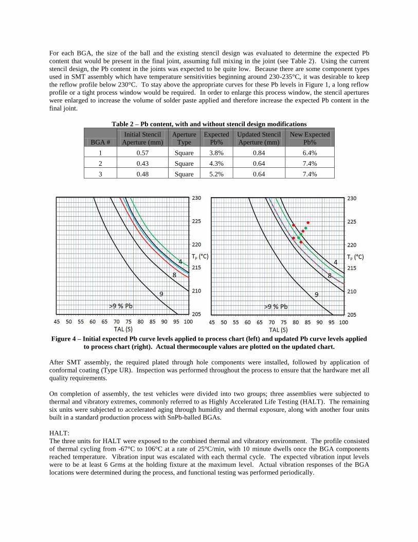
For each BGA, the size of the ball and the existing stencil design was evaluated to determine the expected Pb
content that would be present in the final joint, assuming full mixing in the joint (see Table 2). Using the current
stencil design, the Pb content in the joints was expected to be quite low. Because there are some component types
used in SMT assembly which have temperature sensitivities beginning around 230-235°C, it was desirable to keep
the reflow profile below 230°C. To stay above the appropriate curves for these Pb levels in Figure 1, a long reflow
profile or a tight process window would be required. In order to enlarge this process window, the stencil apertures
were enlarged to increase the volume of solder paste applied and therefore increase the expected Pb content in the
final joint.
Table 2 – Pb content, with and without stencil design modifications
BGA #
Initial Stencil
Aperture (mm)
Aperture
Type
Expected
Pb%
Updated Stencil
Aperture (mm)
New Expected
Pb%
1 0.57 Square 3.8% 0.84 6.4%
2 0.43 Square 4.3% 0.64 7.4%
3 0.48 Square 5.2% 0.64 7.4%
Figure 4 – Initial expected Pb curve levels applied to process chart (left) and updated Pb curve levels applied
to process chart (right). Actual thermocouple values are plotted on the updated chart.
After SMT assembly, the required plated through hole components were installed, followed by application of
conformal coating (Type UR). Inspection was performed throughout the process to ensure that the hardware met all
quality requirements.
On completion of assembly, the test vehicles were divided into two groups; three assemblies were subjected to
thermal and vibratory extremes, commonly referred to as Highly Accelerated Life Testing (HALT). The remaining
six units were subjected to accelerated aging through humidity and thermal exposure, along with another four units
built in a standard production process with SnPb-balled BGAs.
HALT:
The three units for HALT were exposed to the combined thermal and vibratory environment. The profile consisted
of thermal cycling from -67°C to 106°C at a rate of 25°C/min, with 10 minute dwells once the BGA components
reached temperature. Vibration input was escalated with each thermal cycle. The expected vibration input levels
were to be at least 6 Grms at the holding fixture at the maximum level. Actual vibration responses of the BGA
locations were determined during the process, and functional testing was performed periodically.

Accelerated aging:
To induce electronic failures that could be exhibited in the lifetime of fielded hardware, the test units were exposed
to increased temperature and humidity levels. An estimate of the amount of life acceleration that this environment
induced was calculated using a variation of the Arrhenius equation with a humidity stressor applied. This equation
is the Hallberg-Peck Model:
AF = (RHT / RHA) 3 * exp{(Ea/k)*(1/TT-1/TA)}
Given:
RHT Relative humidity in the test environment
RHA Relative humidity in the application environment
Ea Activation energy
k Boltzmann’s constant (k = 8.617 x 10⁻⁵ eV/Tk)
TT Temperature in Kelvin in the test environment
TA Temperature in Kelvin in the application environment
A conservative value of 0.7 was chosen for Activation Energy. For this study, a relative humidity of 60% and
temperature of 30°C was assumed for the application environment. The above formula for test acceleration factor
completed for these values is shown below. Table 3 shows other Acceleration Factors for determining simulated life
based on a range of application conditions.
AF = (0.85/0.60)3 * exp{(0.7/8.617E-5)*(1/358-1/303)}
AF = 2.8 * 61.5 = 174.8
The goal of this study was to fully evaluate the performance of the mixed alloy solder joint over an extended life. In
many aerospace and defense products, this life can be more than 20 years, even 30 years or more. This aging test
was conducted for 63 days to simulate 30 years of aging.
Test time unit: 1 day
Acceleration Factor: 174.8
Simulated Life per day: 174.8/365 = 0.48 years/day
Total test time: 63 days
Total Simulated Life: 30 years
Table 3 – Acceleration factors for various expected service life conditions and the given test conditions.
Expected temperature (K) in Application Environment
20 25 30 35 40 45 50
Ex
pec
ted
RH
in
Ap
pli
cati
on E
nv
iro
nm
ent
0.25 6034.4 3789.7 2416.8 1564.0 1026.2 682.4 459.5
0.30 3492.1 2193.1 1398.6 905.1 593.9 394.9 265.9
0.35 2199.1 1381.1 880.8 570.0 374.0 248.7 167.5
0.40 1473.2 925.2 590.0 381.8 250.5 166.6 112.2
0.45 1034.7 649.8 414.4 268.2 176.0 117.0 78.8
0.50 754.3 473.7 302.1 195.5 128.3 85.3 57.4
0.55 566.7 355.9 227.0 146.9 96.4 64.1 43.2
0.60 436.5 274.1 174.8 113.1 74.2 49.4 33.2
0.65 343.3 215.6 137.5 89.0 58.4 38.8 26.1
0.70 274.9 172.6 110.1 71.2 46.7 31.1 20.9
0.75 223.5 140.4 89.5 57.9 38.0 25.3 17.0
0.80 184.2 115.7 73.8 47.7 31.3 20.8 14.0
0.85 153.5 96.4 61.5 39.8 26.1 17.4 11.7
0.90 129.3 81.2 51.8 33.5 22.0 14.6 9.8
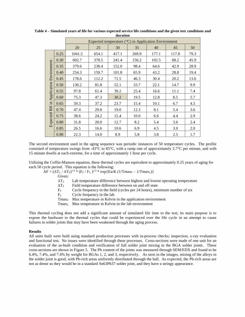
Table 4 – Simulated years of life for various expected service life conditions and the given test conditions and
duration
Expected temperature (°C) in Application Environment
20 25 30 35 40 45 50 E
xp
ecte
d R
H i
n A
pp
lica
tio
n E
nv
iro
nm
ent
0.25 1041.5 654.1 417.1 269.9 177.1 117.8 79.3
0.30 602.7 378.5 241.4 156.2 102.5 68.2 45.9
0.35 379.6 238.4 152.0 98.4 64.6 42.9 28.9
0.40 254.3 159.7 101.8 65.9 43.2 28.8 19.4
0.45 178.6 112.2 71.5 46.3 30.4 20.2 13.6
0.50 130.2 81.8 52.1 33.7 22.1 14.7 9.9
0.55 97.8 61.4 39.2 25.4 16.6 11.1 7.4
0.60 75.3 47.3 30.2 19.5 12.8 8.5 5.7
0.65 59.3 37.2 23.7 15.4 10.1 6.7 4.5
0.70 47.4 29.8 19.0 12.3 8.1 5.4 3.6
0.75 38.6 24.2 15.4 10.0 6.6 4.4 2.9
0.80 31.8 20.0 12.7 8.2 5.4 3.6 2.4
0.85 26.5 16.6 10.6 6.9 4.5 3.0 2.0
0.90 22.3 14.0 8.9 5.8 3.8 2.5 1.7
The second environment used in the aging sequence was periodic instances of 50 temperature cycles. The profile
consisted of temperature swings from -43°C to 85°C, with a ramp rate of approximately 2.7°C per minute, and with
15 minute dwells at each extreme, for a time of approximately 1 hour per cycle.
Utilizing the Coffin-Manson equation, these thermal cycles are equivalent to approximately 0.25 years of aging for
each 50 cycle period. This equation is the following:
AF = (ΔTL / ΔTF)1.9 * (FF / FL )1/3 * exp{Ea/K (1/TmaxF – 1/TmaxL)}
Given:
ΔTL Lab temperature difference between highest and lowest operating temperature
ΔTF Field temperature difference between on and off state
FF Cycle frequency in the field (cycles per 24 hours), minimum number of six
FL Cycle frequency in the lab
TmaxF Max temperature in Kelvin in the application environment
TmaxL Max temperature in Kelvin in the lab environment
This thermal cycling does not add a significant amount of simulated life time to the test; its main purpose is to
expose the hardware to the thermal cycles that could be experienced over the life cycle in an attempt to cause
failures in solder joints that may have been weakened through the aging process.
Results
All units built were built using standard production processes with in-process checks; inspection, x-ray evaluation
and functional test. No issues were identified through these processes. Cross-sections were made of one unit for an
evaluation of the as-built condition and verification of full solder joint mixing in the BGA solder joints. These
cross-sections are shown in Figure 5. The Pb content of the joints was measured through SEM/EDX and found to be
6.4%, 7.4%, and 7.4% by weight for BGAs 1, 2, and 3, respectively. As seen in the images, mixing of the alloys in
the solder joint is good, with Pb-rich areas uniformly distributed through the ball. As expected, the Pb-rich areas are
not as dense as they would be in a standard Sn63Pb37 solder joint, and they have a stringy appearance.

Figure 5 – Micrographs of cross-sections for BGAs 1, 2, and 3 in as-built condition.
The three assemblies subjected to HALT were built into a representation of a higher level assembly and mounted in
the HALT chamber as shown in Figure 6. A vibration survey was performed on each unit to determine the vibration
response at the BGA sites. At the lowest vibration input, the BGAs experience about 5 Grms, and they saw
progressive increases in response as the input was increased, with maximum values of 20, 22, and 27 Grms
experienced at the three BGA sites.
The assembly was exposed to the combined thermal and vibration profile as shown in Figure 7. A thermocouple
located on top of one of the BGAs (the green line in Figure 7) demonstrated good temperature tracking and was used
to ensure that the desired dwell period was reached. At the completion of the fourth thermal cycle, two of the three
units were subjected to the addition period of vibration shown, at the maximum level for 60 minutes. The entire test
lasted for a little over three hours. Units were tested functionally at the end of each dwell period, and during each
transition. Units were also tested approximately every ten minutes during extended vibration. All tests were passed
successfully.
Figure 6 – Unit assembled into test fixture and mounted in the HALT chamber.
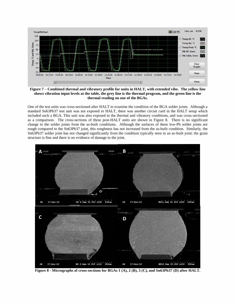
Figure 7 – Combined thermal and vibratory profile for units in HALT, with extended vibe. The yellow line
shows vibration input levels at the table, the grey line is the thermal program, and the green line is the
thermal reading on one of the BGAs.
One of the test units was cross-sectioned after HALT to examine the condition of the BGA solder joints. Although a
standard Sn63Pb37 test unit was not exposed to HALT, there was another circuit card in the HALT setup which
included such a BGA. This unit was also exposed to the thermal and vibratory conditions, and was cross-sectioned
as a comparison. The cross-sections of these post-HALT units are shown in Figure 8. There is no significant
change to the solder joints from the as-built conditions. Although the surfaces of these low-Pb solder joints are
rough compared to the Sn63Pb37 joint, this roughness has not increased from the as-built condition. Similarly, the
Sn63Pb37 solder joint has not changed significantly from the condition typically seen in an as-built joint; the grain
structure is fine and there is no evidence of damage to the joint.
Figure 8 - Micrographs of cross-sections for BGAs 1 (A), 2 (B), 3 (C), and Sn63Pb37 (D) after HALT.
A B
C D

Figure 9 – Thermal cycling profile for accelerated aging test units.
Six test units and four control units (standard SnPb) were subjected to multiple sessions of accelerated aging and
thermal cycling. Electrical acceptance testing was performed between these sessions to verify functionality. In all,
the test units were exposed to 63 days temperature / humidity (85°C / 85% RH) and 200 thermal cycles (See Figure
9) for simulation of approximately 30 years relative to a 60%RH/30°C application environment. The overall flow
for this process is shown in Figure 10.
Figure 10 – Accelerated aging process flow
All ten test units successfully passed testing until the final round of aging. In the final test, two of the six mixed-
alloy units failed a test, indicating a problem with BGA 1. One of the mixed-alloy units subjected to accelerated
aging was cross-sectioned, as well as one of the Sn63Pb37 units, to evaluate the resulting condition of the solder
joints (see Figure 11). The cross sectional images of the post-aging units do not show any significant anomalies in
the solder joints; there were no fractured solder joints, no crack initiation sites, and generally no apparent
deterioration of the solder joints. The mixed-alloy joints still display a uniform distribution of Pb-rich areas of
relatively fine grain structure. In the post-aging image for the standard SnPb joint, however, there is a significant
amount of grain growth. The grain structure of the joint is not as fine as in the as-built condition. Dye-and-pry was
Te
m
p
er
at
ur
e
(°
C)

used to evaluate the failed units, and there was no indication of solder joint failure from this inspection; the printed
circuit board pad was partially or fully lifted at all joints as a result of the component removal.
Figure 11 - Micrographs of cross-sections for BGAs 1 (A), 2 (B), 3 (C), and Sn63Pb37 (D) after accelerated
aging.
Conclusions
BGAs with SAC305 balls were inserted into an existing military design and installed using a backward compatible
process (SnPb solder). The assembly process was modified slightly (solder paste application and reflow profile)
according to guidelines developed in previous studies to accommodate these Pb-free components, but kept within a
window suitable for typical SnPb assembly. Cross-section evaluations of the base-line units validate that the process
used resulted in complete mixing of the solder joints.
These assemblies were subjected to HALT and accelerated aging environments similar to those used in production
development evaluations. The units survived nearly all functional testing through these environments,
demonstrating survivability of the mixed alloy solder joints under exposure to humidity, temperature, vibration, and
thermal cycling. The only failures exhibited came after a significant amount of aging and testing was complete, and
were attributed to component failure, not solder joint failure.
This study shows that when the parameters of a backward compatible process are appropriately controlled and
applied, the resulting BGA solder joint can have acceptable reliability in a military product for certain expected
environmental conditions. We must keep in mind, however, that this relies on certain assumptions about the
behavior of a low-Pb solder joint. Testing of Pb-free solder has demonstrated that reliability can be dependent on the
parameters of the test and the order of certain testing. More studies should be performed to further investigate the
point or range at which the Pb-content of a solder joint results in Pb-free-like behavior or standard SnPb-like
behavior.
A B
C D

One observation of unique interest in this study is the lack of change in the morphology of the mixed-alloy solder
joints. The Sn63Pb37 solder joints show a marked change in structure, with significant grain growth through both
thermal cycling and accelerated aging in temperature and humidity. The mixed-allow joints do not show the same
amount of change in shape of the lead-rich areas.
Bibliography:
[1] A. Dasgupta, P. Sharma, and K. Upadhyayula, “Micro-mechanics of fatigue damage in Pb–Sn solder due to
vibration and thermal cycling,” Int. J. Damage Mech., vol. 10, no. 2, April 2001, pp. 101–132.
[2] C. Basaran and Y. Wen, “Grain growth in eutectic Pb/Sn ball grid array solder joints,” Proc. Inter Society Conf.
Thermal Phenomena, 2002, pp. 903–908.
[3] Snugovsky, P., Zbrzezny, A.R., Kelly, M. and Romansky, M., “Theory and practice of lead-free BGA assembly
using Sn-Pb solder”, CMAP International Conference on Lead-free Soldering, Toronto, Canada, 2005.
[4] F. Hua, R. Aspandiar, T. Rothman, C. Anderson, G. Clemons, and M. Klier, “Solder joint reliability of SnAgCu
BGA components attached with eutectic SnPb solder paste,” J. Surf. Mount Technol. Assoc., vol. 16, no. 1, 2003,
pp. 34–42.
[5] Sun, F., “Solder joint reliability of Sn-Ag-Cu BGA and Sn-Pb solder paste”, Proceedings of 2005 IEEE 6th
International Conference on Electronic Packaging Technology, Shenzhen, China, 2005.
[6] D. Hillman, M. Wells, and K. Cho, “The impact of reflowing a leadfree solder alloy using a SnPb solder alloy
reflow profile on solder joint integrity,” Proc. Int. Conf. Lead-free Soldering, Toronto, ON, Canada, May 2005.
[7] G. Grossmann, J. Tharian, P. Jud, and U. Sennhauser, “Microstructural investigation of lead-free BGAs soldered
with tin–lead solder,” Soldering & Surface Mount Technology, vol. 17, no. 2, Feb. 2005, pp. 10–21.
[8] H. McCormick, P. Snugovsky, Z. Bagheri, S. Bagheri, C. Hamilton, G. Riccitelli, and R. Mohabir, “Mixing
metallurgy: Reliability of SAC balled area array packages assembled using SnPb solder,” J. Surf. Mount Technol.
Assoc., vol. 20, no. 2, 2007, pp. 11–18.
[9] D. Nelson, H. Pallavicini, Q. Zhang, P. Friesen, and A. Dasgupta, “Manufacturing and reliability of lead-free and
mixed system assemblies (Snpb/lead-free) in avionics,” J. Surf. Mount Technol. Assoc., vol. 17, no. 1, 2004, pp. 17–
24.
[10] Gregorich, T. and Holmes, P., “Low-temperature, high reliability assembly of of lead-free CSPS”, IPC/JEDEC
4th International Conference on Lead-free Electronic Components and Assemblies, Frankfurt, Germany, 2003.
[11] Zbrzezny, A.R., Snugovsky, P., Lindsay, T. and Lau, R., “Reliabilty investigation of Sn-Ag-Cu BGA memory
modules assembled with Sn-Pb eutectic paste during different reflow profiles”, CMAP International Conference on
Lead-free Soldering, Toronto, Canada, 2005.
[12] Zbrzezny, A.R., Snugovsky, P., Lindsay, T. and Lau, R., “Reliabilty investigation of mixed BGA assemblies”,
IEEE Transactions on Electronics Packaging Manufacturing, 29 (3), 2006, pp. 211-216.
[13] Handwerker, C., “Transitioning to lead free assemblies”, Printed Circuit Design and Manufacturing, March
2005.
[14] Pan, J., “Estimation of liquidus temperature when SnAgCU BGA/CSP components are soldered with SnPb
paste”, Proceedings of 2006 IEEE 2006 7th International Conference on Electronics Packaging Technology,
Shanghai, China, 2006.
[15] Shea, C., Pandher, R., Hubbard, K., Ramakrishna, G., Syed, A., Henshall, G., Chu, Q., Tokotch, N., Escuro, L.,
Lapitan, M., Ta, G., Babasa, A., Wable, G., “Low-silver BGA assembly phase I – reflow considerations and joint
homogeneity initial report”, Proceedings of 2008 IPC APEX Conference, Las Vegas, NV, 2008.
[16] Shea, C., Pandher, R., Hubbard, K., Ramakrishna, G., Syed, A., Henshall, G., Chu, Q., Tokotch, N., Escuro, L.,
Lapitan, M., Ta, G., Babasa, A., Wable, G., “Low-silver BGA assembly phase I – reflow considerations and joint
homogeneity second report: SAC105 spheres with tin-lead paste”, Proceedings of 2008 SMTA International,
Orlando, FL, 2008.
[17] Shea, C., Pandher, R., Hubbard, K., Ramakrishna, G., Syed, A., Henshall, G., Chu, Q., Doxtad, E., Santos, M.,
Lapitan, M., Solon, J., Babasa, A., Wable, G., “Low-silver BGA assembly phase II – reflow considerations and joint
homogeneity third report: comparison of four low-silver sphere alloys and assembly process sensitivities”,
Proceedings of 2009 IPC APEX Conference, Las Vegas, NV, 2009.
[18] Shea, C., Pandher, R., Hubbard, K., Ramakrishna, G., Syed, A., Henshall, Fehrenbach, M., G., Chu, Q., Wable,
G., “Low-silver BGA assembly phase II – reflow considerations and joint homogeneity fourth report: sensitivity to
process variations”, Proceedings of 2009 SMTA International, San Diego, CA, 2009.
[19] B. Fox, B. Gumpert, L. Woody, “Development of Processing Parameters for Soldering Lead-Free Ball Grid
Arrays Using Tin-Lead Solder”, Proceedings of 2009 SMTA International, Orlando, FL, 2012


