Halme, Janne; Miettunen, Kati; Lund, Peter Effect of ...
53
This is an electronic reprint of the original article. This reprint may differ from the original in pagination and typographic detail. Powered by TCPDF (www.tcpdf.org) This material is protected by copyright and other intellectual property rights, and duplication or sale of all or part of any of the repository collections is not permitted, except that material may be duplicated by you for your research use or educational purposes in electronic or print form. You must obtain permission for any other use. Electronic or print copies may not be offered, whether for sale or otherwise to anyone who is not an authorised user. Halme, Janne; Miettunen, Kati; Lund, Peter Effect of Nonuniform Generation and Inefficient Collection of Electrons on the Dynamic Photocurrent and Photovoltage Response of Nanostructured Photoelectrodes Published in: Journal of Physical Chemistry C DOI: 10.1021/jp806512k Published: 25/12/2008 Document Version Peer reviewed version Please cite the original version: Halme, J., Miettunen, K., & Lund, P. (2008). Effect of Nonuniform Generation and Inefficient Collection of Electrons on the Dynamic Photocurrent and Photovoltage Response of Nanostructured Photoelectrodes. Journal of Physical Chemistry C, 112(51), 20491-20504. https://doi.org/10.1021/jp806512k
Transcript of Halme, Janne; Miettunen, Kati; Lund, Peter Effect of ...

This is an electronic reprint of the original article.This reprint may differ from the original in pagination and typographic detail.
Powered by TCPDF (www.tcpdf.org)
This material is protected by copyright and other intellectual property rights, and duplication or sale of all or part of any of the repository collections is not permitted, except that material may be duplicated by you for your research use or educational purposes in electronic or print form. You must obtain permission for any other use. Electronic or print copies may not be offered, whether for sale or otherwise to anyone who is not an authorised user.
Halme, Janne; Miettunen, Kati; Lund, PeterEffect of Nonuniform Generation and Inefficient Collection of Electrons on the DynamicPhotocurrent and Photovoltage Response of Nanostructured Photoelectrodes
Published in:Journal of Physical Chemistry C
DOI:10.1021/jp806512k
Published: 25/12/2008
Document VersionPeer reviewed version
Please cite the original version:Halme, J., Miettunen, K., & Lund, P. (2008). Effect of Nonuniform Generation and Inefficient Collection ofElectrons on the Dynamic Photocurrent and Photovoltage Response of Nanostructured Photoelectrodes.Journal of Physical Chemistry C, 112(51), 20491-20504. https://doi.org/10.1021/jp806512k

1
Effect of non-uniform generation and inefficient
collection of electrons on the dynamic
photocurrent and photovoltage response of
nanostructured photoelectrodes
Janne Halme*, Kati Miettunen, Peter Lund
Laboratory of Advanced Energy Systems, Department of Engineering Physics, Faculty of
Information and Natural Sciences, Helsinki University of Technology, P.O. BOX 5100,
FIN-02015 TKK, Finland
Tel.: +35894513217, Fax: +35894513195, E-mail: [email protected]
Title running head: Dynamic response of nanostructured photoelectrodes
* Corresponding author

2
ABSTRACT
This paper investigates how non-uniform generation and inefficient collection of
electrons influence the dynamic photocurrent and photovoltage response of
nanostructured photoelectrodes. The standard diffusion model theory of small amplitude
light intensity modulated photocurrent (IMPS) and photovoltage (IMVS) spectroscopy is
refined and generalized to an arbitrary electron generation profile, allowing
straightforward coupling to any optical model. Expressions are derived for the local
electron concentration, and IMPS and IMVS transfer functions, for localized, uniform,
and exponential generation profiles. Both limited collection and non-uniform generation
of electrons modify the photoelectrode thickness (d) dependence of the characteristic
IMPS and IMVS time constants and complicate their interpretation. This can lead to
significant overestimation of the electron diffusion coefficient, diffusion length and
collection efficiency when using common approximate relations. With near contact
electron generation, the IMPS response exhibits two time-constants, only the slower one
of which corresponds to electron transport across the film and scales with d. In the
presence of this effect it is possible that in case of two equally thick samples, the one with
smaller electron diffusion coefficient displays apparently faster electron transport. These
errors demonstrated by experimental IMPS data of pressed TiO2 photoelectrodes can be
minimized by using modulated light incident from the counter electrode side, and
avoided when analyzing the ratio of IMPS at opposite directions of illumination.
KEYWORDS: dye-sensitized, photovoltaic, light absorption, recombination, collection
probability, Dirac’s delta

3
1 Introduction
Electrochemical solar cells based on nanostructured photoelectrodes is a promising
approach to cost-effective utilization of solar energy. The most well known device of this
type is the dye solar cell (DSC)1,2. In DSC, light absorption occurs by dye molecules
attached on wide-band gap semiconductor nanoparticles that form a nanoporous film.
Upon light absorption, an electron is injected from the dye to the semiconductor. It
thereafter travels by diffusion in the nanoparticle network until it is collected at the
substrate contact or is lost via recombination reactions. The oxidized dye is regenerated
by a hole transport medium, typically a liquid redox electrolyte solution, that fills the
pores of the film.
The capability of the cell to produce photocurrent is described by the incident-photon-
to-collected-electron efficiency (IPCE), also known as the external quantum efficiency
(EQE). It is defined as the number of electrons delivered by the solar cell to the external
circuit per number of photons incident on the cell, and can be expressed as a product of
the partial quantum efficiencies of light harvesting (LH), electron injection (INJ) and
electron collection (COL)
APCELHCOLINJLHIPCE (1)
where further division to an optical (LH) and electrical part is achieved by defining the
absorbed-photon-to-collected-electron efficiency (APCE).
While the best DSCs reach IPCE over 95 %3, the photocurrent of most practical solar
cells is significantly lower than what would be expected based on their optical properties.
It is therefore necessary to separate and quantify experimentally the injection and
collection parts of eq 1 from DSCs under realistic working conditions. This problem was

4
recently addressed by combining IPCE measurements with optical characterization to
estimate the steady-state APCE, and using the standard electron diffusion model4 to
decouple its INJ and COL parts5.
Quantifying COL is of particular interest for optimizing flexible plastic DSCs that
usually suffer from poor electron transport in their low-temperature-prepared
photoelectrodes, but also for fundamental investigations of the transport phenomena in
disordered nanostructured photoelectrodes. Instead of the direct steady-state approach5,
the standard practice has been to estimate COL indirectly, using dynamic techniques such
as intensity modulated photocurrent (IMPS)6 and photovoltage (IMVS)7,8 spectroscopy.
Interpreting the IMPS and IMVS response by the time-dependent standard diffusion
model9 yields estimates for the electron diffusion coefficient (D) and lifetime (),
respectively, which allows further estimation of the electron diffusion length10
DL (2)
The diffusion length it is one of the key parameters determining COL. To make a high
performance cell, L needs to be larger than the photoelectrode film thickness: when L
exceeds twice the film thickness, less than 10 % of electrons generated uniformly over
the film are lost by recombination at the short circuit5. However, it was recently shown
by theoretical arguments that IMPS and IMVS are unable to yield correct estimates for
the steady state values of D and for nanostructured semiconductor photoelectrodes,
since the dynamic response is dominated by filling and emptying of a large density of
trap states distributed in energy in the semiconductor band gap11. This challenges the
reliability of using dynamic techniques to estimate L and COL relevant to the steady state
5
photovoltaic performance of DSC – a question that remains to be addressed
experimentally.
Investigation of this problem could be feasible by comparing COL estimates
determined by dynamic and steady state measurements in same conditions. The steady
state approach is based on varying the photoelectrode film thickness (d), direction of
illumination, and penetration depth of light, so that L falls within the examined d range,
and thus, brings about measurable photocurrent losses due to electron recombination5. To
compare with the dynamic techniques, the effects of these conditions on the IMPS and
IMVS response needs to by well understood and quantified, and this is the main purpose
of the present paper.
In practical IMPS experiments, weakly absorbed light is usually used for the intensity
modulation to realize roughly uniform electron generation profile in the photoelectrode
film12,13. Alternatively, strongly absorbed light, incident from the counter electrode side,
is used to generate electrons far from the substrate contact to measure their transit time
across the film14,15. In both cases, recombination losses at the short circuit condition are
often neglected in the data analysis, and hence, COL is implicitly assumed, or
rationalized by the data, to be close to 100%.
In the present paper, we generalize the standard diffusion model theory of light
intensity modulated response of nanostructured photoelectrodes to readily comply with
any (arbitrary) electron generation profile. We use the theory to investigate how non-
uniform generation and limited collection of electrons affect the IMPS and IMVS
characteristics. The aim is to establish a clear understanding of these effects, identify
problems that they induce to practical data analysis, and point out ways to avoid them.

6
Although the analysis of this paper neglects many details of the electron transport and
recombination dynamics in nanostructured photoelectrodes, such as electron trapping, the
theoretical results, demonstrated by experiments, provide a necessary background for
understanding and validating more detailed electron transport theories that build on the
standard diffusion model.
2 Theory
2.1 Approximate IMPS and IMVS analysis
IMPS and IMVS are used to evaluate electron transport and recombination in DSCs in
order to identify materials and methods that enhance their COL. The characteristic time
constant of the IMVS response7,8, IMVS, is interpreted as the electron lifetime , and
equals with the relaxation (RC) time-constant of photoelectrode film measurable by
electrochemical impedance spectroscopy12 or photovoltage decay16 at the same
conditions. The characteristic IMPS time constant, IMPS, for its part, is a measure of the
mean arrival time of photogenerated electrons at the photoelectrode substrate contact, and
is related to the electron diffusion coefficient by an approximate relation14
IMPS
2
daD (3)
where d is the thickness of the photoelectrode film. The proportionality constant a
depends on the electron generation profile. For example, for uniform generation a ≈
0.393, and for generation localized at the bulk electrolyte side of the film, a ≈ 0.428
(values determined in the present work, cf.14,15). Eq 3 is widely used in the analysis of
IMPS data, but it is strictly speaking valid only when recombination can be neglected17.

7
For cells with limited COL, loss of electrons by recombination during their transport
affects IMPS, and hence the D estimate by eq 3. Consequently, most IMPS studies do not
pursue quantitative estimation of L, but rather adhere to ranking different samples by the
relative magnitude of their measured IMPS and IMVS.
Based on these time constants, the electron collection efficiency can be estimated
roughly as12,18
IMVS
IMPSCOL 1
(4)
but also this relation is accurate only for relatively high values of COL18. Hence, neither
eq 3 nor 4 are particularly suitable for accurate evaluation of dynamic electron transport
and collection in practical DSCs that show limited COL, or for quantitative comparison to
the steady state methods5 that work best when COL is low.
In this paper, we use the time-dependent standard diffusion model to investigate the
failure of eqs 3 and 4 due to non-uniform electron generation and limited electron
collection. We start by reviewing and slightly reformulating the diffusion model for
IMPS and IMVS analysis, and summarize the analytical results for different electron
generation profiles.
2.2 Time-dependent standard diffusion model with small amplitude light intensity modulation
The theoretical framework for the present work is the well established one-dimensional
differential equation model for the electron generation, transport and recombination in a
nanostructured semiconductor photoelectrode permeated with a redox electrolyte (called
hereafter the diffusion model), summarized in Appendix A. We should emphasize that,

8
among other details of electron transport and recombination dynamics, this model
explicitly neglects electron trapping that in reality can dominate experimental IMPS and
IMVS response. However, it turns out to be necessary to generate thorough
understanding of the characteristics of this simple model to support development and
experimental verification of more complex models.
In IMPS and IMVS, the dynamic response of the cell to a small amplitude sinusoidal
modulation of the incident light intensity is measured as a function of the angular
modulation frequency . The incident photon flux constitutes a monochromatic
modulated (AC) part AC superimposed on a constant background (DC) part DC
tieΦtΦΦtΦ 1),(),( DCACDC (5)
where the modulation depth is typically set less than 0.1 to maintain linearity of the
response.
As the incident light beam traverses the photoelectrode film its intensity is attenuated
by light absorption, and hence the local absorption rate varies with position in the film.
To treat this formally, we define the spatial light harvesting efficiency fLH(x), with units
m-1, as the probability per unit length that a photon incident on the cell is absorbed at the
position x within the photoelectrode film, with x = 0 at the substrate contact. fLH defines
the light absorption profile and is related to the overall light harvesting efficiency LH as
d
dxxf0
LHLH )( (6)
where d is the photoelectrode film thickness. By defining LH with respect to the photon
flux incident externally on the photoactive area of the cell, fLH includes all optical effects
and losses relevant to the optical conditions in question.

9
The spatial electron generation rate is assumed equal to the spatial light absorption rate
that scales linearly with the incident photon flux (m-2s-1), multiplied by a position-
independent electron injection efficiency,
)(),(),( LHINJ xftΦtxg (7)
The spatial distribution of electron generation is thus defined by fLH, whereas its time-
dependence follows the light modulation.
2.3 IMPS transfer function
The IMPS transfer function (F*IMPS) has been defined earlier as the ratio of the
harmonically modulated incident photon flux (excitation) and the resulting photocurrent
density iAC of the cell (response)
x
N
Φ
D
x
tn
tΦ
D
tΦq
tiF
)),0(),,0(
),(),(
),()(
DC
ACe,
ACACe
ACIMPS
(8)
where we have used eqs 5 and A5 and the Fick’s law of diffusion (see Appendix A for
notation). At the limit of small modulation amplitude at the steady state and short circuit
condition, eq 8 is equal to the differential IPCE of the cell
DIFCOL,INJLH
DC
SC
e
DIFIPCE,
1
Φ
i
q (9)
where iSC is the steady state short circuit current density, COL,DIF the differential electron
collection efficiency, and qe the elementary charge. In reality, the short circuit current of
DSC may not be exactly linear with the incident light intensity5,10,19, meaning that
IPCE,DIF varies with the intensity, and differs from the absolute IPCE that is defined
instead as

10
COLINJLH
DCe
SCIPCE
Φq
i (10)
The light intensity dependence of IPCE,DIF is considered to be solely due to COL,DIF,
whereas LH and INJ can be normally assumed intensity independent. Eqs 9 and 10
imply that the quantum efficiency of electron generation GEN = LHINJ acts as a
frequency-independent scaling factor for the photocurrent output. Hence, instead of eq 8,
it is useful to define the IMPS transfer function as the frequency dependent differential
electron collection efficiency
x
N
Φ
DFF
)),0()(
)(INJLHDCINJLH
IMPSIMPS
(11)
that at the steady state short circuit condition equals the differential electron collection
efficiency (cf. eq 9)
),0( EXTIMPSDIFCOL, kF (12)
This IMPS definition (eq 11) is ideal for systematic analysis of the electron collection
problem and will be used throughout the present paper.
2.4 IMVS transfer function
The IMVS transfer function (F*IMVS) relates the dynamic excitation of the incident
photon flux to the AC photovoltage (VAC) that is further related to the electron
concentration at the substrate contact
)0(
),0(
0),(
),,0(
),(
),()(
eDCeACe
ACe,
ACe
AC
IMVSCΦ
N
xn
V
tΦq
tn
tΦq
tVF
(13)
by the differential (chemical) capacitance (per unit volume) of the photoelectrode, Ce

11
V
nqC
e
ee (14)
In DSC, Ceis a specific property of the photoelectrode – electrolyte material system. It is
also a function of the electron concentration12,20, and hence, its value at the substrate
contact, Ce(0) depends on the operating conditions of the cell. Nevertheless, it does not
affect the frequency dependence of eq 13, but only its magnitude. For the present
theoretical investigations, it is therefore more practical to define the IMVS transfer
function based on electron concentration at the contact
INJLHDCACINJLH
ACe,
IMVS
),0(
),(
),,0()(
Φ
N
tΦ
tnF (15)
where we also account for the quantum efficiency of electron generation in analogy with
the IMPS definition (eq 11).
Finally, we point out that in the case of the kinetic boundary condition (eqs A2a, A7a),
the IMPS and IMVS transfer functions are related in a particularly simple manner. Since
the photocurrent and thus the IMPS transfer function are proportional to the electron
concentration at the substrate contact (cf. eqs A7a and 11):
),0()(INJLHDC
EXTIMPS
N
Φ
kF (16)
the transfer functions are related as
)()0()( IMVSEXTeIMPS FkCF (17)
)()( IMVSEXTIMPS FkF (18)
This means that if experimental conditions are arranged corresponding to a finite constant
kEXT, it makes no difference to the dynamic information whether one measures the IMPS
or the IMVS response. In practice this can be realized simply by using an external

12
measure resistor in series with the cell, the current and voltage over which are naturally
proportional to each other. Usually however, IMPS is measured at the short circuit and
IMVS at the open circuit condition and this distinction will be adopted also here. Owing
to the different value of kEXT, the dynamic response is characteristically different in these
cases.
2.5 Measurable IMPS and IMVS response
To simplify the present theoretical investigations, two factors affecting the
experimentally measured IMPS and IMVS response are neglected.
Firstly, while the IMPS transfer function is defined here as a frequency-dependent
collection efficiency (eq 11), experimental IMPS data is actually measured with respect
to the photocurrent density (eq 8) and include therefore the quantum efficiency of
electron generation, GEN = LHINJ, as an unknown factor (eq 9). This causes a scaling
problem in the interpretation of the measured IMPS data, as discussed below. The scaling
factor in the measured IMVS data is correspondingly LHINJ/Ce(0) (cf. eqs 13 and 14).
Secondly, the measured IMPS response (but not IMVS) of the photoelectrode film is
attenuated due to impedance of other cell components, an effect known as RC
attenuation6,21,22. The photocurrent signal measured in the external circuit (F*IMPS,EXT) is
)()()( IMPSAEXTIMPS, FFF (19)
where F*IMPS is the non-attenuated response given by eq (8) and FA the attenuation factor
that can be written generally as
)()(
)()(
SP
PA
ZZ
ZF
(20)

13
where ZS and ZP are the impedances connected respectively in series and parallel with the
photoelectrode film. In practice, the main contribution to ZS is the Ohmic series resistance
RS of the cell, whereas ZP is given by the combined capacitance CPE of the photoelectrode
film and the substrate – electrolyte interface, the latter dominating close to short circuit
condition. The RC attenuation may dominate the high-frequency end of the IMPS
response6,21,23, but can accounted for by measuring FA independently by impedance
spectroscopy at the same conditions, and minimizing RS and CPE by cell design.
2.6 Solutions for different electron generation profiles
Having defined the theoretical framework we turn to the main topic of the paper,
namely, theoretical analysis of the effect of the electron generation profile, film thickness
and electron diffusion length on IMPS and IMVS response. To determine expressions for
the IMPS and IMVS transfer functions (eqs 15 and 16), eq A6 needs to be solved for the
AC part of the electron concentration, N(x,). We begin by considering an arbitrary
spatially varying electron generation.
2.6.1 Arbitrary generation
Since eq A6 is a linear ordinary differential equation, it follows from the principle of
superposition that that the solution of eq A6 for any arbitrary generation term G(x) (eq
A4) can be obtained readily as
dxNfxN
d
0
LH ),()()( (21)
where N is the solution of eq A6 for a Dirac’s -function generation, given by eq 23
below. The mathematical derivation of this result is provided as Supporting Information.

14
The result means that determining the local electron concentration profile, as well as
the IMPS and IMVS transfer functions, for any fLH(x), is a task as easy as performing the
integration in eq 21. For an fLH(x) not too complicated, as in all the cases of the present
paper, this integration is straightforward analytically. More generally, one may find it
sufficient and convenient to work with eq 21 numerically, irrespective of whether an
analytical solution exists or not. Particularly useful this will be in cases where one is
restricted to numerical fLH(x) data, e.g. from optical simulations.
In essence, eq 21 couples the standard diffusion model to any optical model describing
spatial variation of photon flux in the photoelectrode film. In the following, we
summarize briefly the analytical results for certain generation profiles of practical and
theoretical interest, and discuss some limiting cases.
2.6.2 Localized generation
In the purely theoretical case of localized electron generation, the spatial light
harvesting efficiency is
),(),( LH xxf (22)
where (x,) is the Dirac’s delta function localized at x = . The solution Nof eq A6 for
the localized generation term (eqs A4 and 22) is
)u())(sinh(
)cosh()sinh(
)sinh()cosh())(cosh(),(
EXT
EXTINJLHDC
xx
dkdD
xkxDd
D
ΦxN
(23)
where
i
D
11 (24)

15
and u(x – ) is the unit step function. The mathematical derivation of eq 23 is given as
Supporting Information.
IMPS
The IMPS transfer function at the short circuit becomes (eqs 16 and 23 with kEXT ∞)
)cosh(
))(cosh(SC,IMPS,
d
dF
(25)
As the locus of generation approaches the collecting contact ( = 0) the IMPS response
becomes unity, and the dynamic photocurrent response is pushed to high frequencies,
whereas for localized generation at the electrolyte side of the film
d
F
cosh
1SC,IMPS, ( = d) (26)
Eq 26 has a particularly useful interpretation. In the limit of steady state ( 0) it gives
the (differential) spatial electron collection efficiency24
L
d
L
d
cosh
cosh
)(DIF,COL,
(27)
This is the probability at which electron injected to the film at x = will reach the
collecting contact by diffusion before being lost by recombination. The overall collection
efficiency of electrons generated in the film according to a profile fLH(x) is then nothing
else but the weighted average of the spatial collection efficiency12
d
d
dxxf
dxxxf
0
LH
0
DIF,COL,LH
COL
)(
)()(
(28)

16
This is a consequence of the fact that in our model, the electrons perform pure Fickian
diffusion, i.e. their transport is independent of their local concentration.
It is worth mentioning that the spatial collection efficiency should be useful also for
estimating the fraction of electrons lost by recombination in charge extraction
experiments25,26. In that case the generation profile in eq 28 is replaced by the electron
concentration profile established in the film prior to the extraction step.
IMVS
The IMVS transfer function for the localized generation at the open circuit condition
(kEXT 0) is
)sinh(
))(cosh(OC,IMVS,
dD
dF
(29)
In the special case of near-contact generation this reduces to
)coth(1
OC,IMVS, dD
F
( = 0) (30)
and for the generation at the opposite end of the film to
)sinh(
1OC,IMVS,
dDF
( = d) (31)
Interestingly, the IMVS response for -generation at the contact (eq 30) has exactly the
same mathematical form as the general transmission line impedance describing transport
and interfacial transfer of electrons in porous electrode films27. Indeed, the diffusion
model is equivalent to a transmission line model28. The exact correspondence of eq 30 to
impedance arises from the fact that in both cases, electron current is injected to the film at
the same location where the potential is measured, i.e. at the contact. For the same reason,
eq 31 does not correspond to impedance.
17
2.6.3 Uniform generation
In the case of uniform light absorption, the electron generation is constant over the
photoelectrode film. If in this hypothetical case, we fix the light harvesting efficiency to
LH, the spatial light harvesting efficiency becomes
d
xf LHUNI
(32)
and the modulated spatial electron concentration is
1)cosh(
)cosh()sinh(
)sinh()cosh()sinh()(
EXT
EXT
2
LHINJDC
UNI xdkdD
xkxDd
Dd
ΦxN
(33)
IMPS
The short circuit IMPS transfer function for the uniform electron generation is then
)tanh(1
UNISC,IMPS, dd
F
(34)
It is noteworthy that in the limit L >> d, the IMPS response for the uniform generation
(eq 34) becomes mathematically equivalent to the finite-length Warburg impedance of
diffusion29
)tanh(1
UNISC,IMPS, isis
F ; D
ds
2 (L >> d) (35)
whereas in the limit L << d, it approaches the form of the Gerischer impedance
i
FF G
1UNISC,IMPS, ;
d
LFG (L << d) (36)
that is a good model for the impedance of a porous charge transfer electrode when L <<
d27. This is of course no coincidence since as already mentioned, both the IMPS response
and impedance follow from the same electron transport problem28.
18
Note also that in the limit of poor electron collection (L << d), the steady state value of
FIMPS, i.e. the (differential) electron collection efficiency, is given by the ratio of the
diffusion length to the film thickness (eq 36). In other words, the usual conception, that
only those electrons that are generated within distance L from the contact will be
collected, is a good approximation when (but only when) L << d.
IMVS
The open circuit IMVS transfer function for its part, becomes for the uniform
generation
2UNIOC,IMVS,
1
dDF (37)
that simplifies further to
1
UNIOC,IMVS,
11
i
dF (38)
Eq 38 represents a perfect semicircle in the complex plane, characterized by a single time
constant, the electron lifetime . This is understandable since for uniform generation and
no collection (open circuit), the electron concentration remains always constant over the
film and hence, electron diffusion does not play a role in the dynamic response.
2.6.4 Exponential generation
A more realistic model for the IMPS and IMVS response of DSC is obtained when the
electron generation is assumed exponential corresponding to absorption of
monochromatic light according to the Beer-Lambert law. Depending whether the
modulated light is incident on the photoelectrode (PE) or counter electrode (CE) side, the
spatial light harvesting efficiency is
19
xeRTxf DPETCOPE 1 (PE side illumination) (39)
)(
DPEELCECE 1 dxeRTTxf (CE side illumination) (40)
where D and are respectively the monochromatic light absorption coefficient of the
dye and the total monochromatic absorption coefficient of the photoelectrode film,
including e.g. light absorption by the triiodide ions in the electrolyte within the pores of
the film. TTCO, TCE and TEL are the transmittances of the photoelectrode substrate, the
counter electrode and the bulk electrolyte layer, respectively, and RPE is the reflectance of
the photoelectrode film5.
Analytical integration of eq 21 for these exponential profiles yields results that are
equivalent to those derived earlier6, with the difference that here, we explicitly include
optical losses in the expressions. This being the case, it suffices only to briefly summarize
the results according to our notation.
At the PE side illumination,
xexkAxDAD
ΦRTxN
)sinh()()cosh()1(
)(
1)( EXTPEPE22
INJDCDPETCO
PE
(41)
where
)cosh()sinh(
)cosh()sinh(
EXT
PEdkdD
eddA
d
(42)
and the electron concentration at the collecting contact is
PE22
INJDCDPETCOPE
1)0( A
ΦRTN
(43)
The solution for the CE side illumination is obtained by replacing with - in eqs 41
and 42 and multiplying thereafter by exp(-d) (cf. eq 40):

20
dx eexkAxDAD
ΦRTTxN
)sinh()()cosh()1(
)(
1)( EXTCECE22
INJDCDPEELCECE
(44)
where
)cosh()sinh(
)cosh()sinh(
EXT
CEdkdD
eddA
d
(45)
and the electron concentration at the contact is
deA
ΦRTTN
CE22
INJDCDPEELCECE
1)0( (46)
IMPS
Noting that for the exponential generation profiles (eqs 39 and 40), LH is obtained
form eq 6, the IMPS transfer functions for the PE and CE illumination are obtained by
using eqs 43 and 46 in eq 16:
PE22
EXTPEIMPS,
1A
e
kF
d
(47)
d
deA
e
kF
CE22
EXTCEIMPS,
1 (48)
which at the short circuit (kEXT ∞) reduces to
1
)cosh()tanh(
122
2
PESC,IMPS,d
ed
eF
d
d
(49)
1)cosh(
)tanh(122
2
CESC,IMPS,d
ed
e
eF
d
d
d
(50)
IMVS
The IMVS transfer function follows from the above IMPS expressions directly by eq
18. At the open circuit (kEXT 0), the IMVS responses are therefore

21
)sinh()coth(1
122PEOC,IMVS,
d
ed
eDF
d
d
(51)
)sinh()coth(1
122CEOC,IMVS,
d
ed
eD
eF
d
d
d
(52)
3 Results and discussion
Next we investigate in detail the characteristics of the IMPS and IMVS transfer
functions with respect to variation of the photoelectrode film thickness, generation profile
and diffusion length. This is done first qualitatively in terms of the characteristic shapes
and trends in the IMPS and IMVS spectra, and thereafter quantitatively in terms of the
characteristic time constants, IMPS and IMVS, and estimation of L and COL.
Unless otherwise stated, the following standard set of parameters is used throughout the
paper: d = 30 m, 1/ = 5 m, L = 10 m, = 16 ms, i.e. (2)-1 = 10 Hz, and D =
6.25·10-6 m2/s.
3.1 Characteristics of the IMPS and IMVS spectra
3.1.1 Localized and uniform generation
The extreme cases of localized (-function) and uniform (flat) generation profiles
(Figures 2 and 3) are ideal for illustrating the characteristics of the time-dependent
diffusion model.
IMPS
The IMPS response is typically dominated by a single time constant that varies with the
photoelectrode film thickness or locus of generation (Figure 2). However, the response is
never a perfect semicircle in the complex plane, but exhibits marked frequency dispersion
22
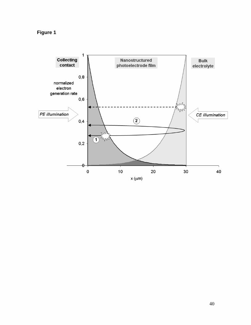
that can be identified as a flattened arc (Figure 2a), spiraling to the origin (Figures 2a and
2b), or a 45º slope at the high frequencies (Figure 2c).
These effects can be understood by realizing that the IMPS spectrum is effectively a
measure the number and arrival time of electrons reaching the collecting contact6,9,21: The
spiraling occurs at the frequency scale where the transport time of electrons from the
point of generation to the contact is slow enough to cause a phase difference over 90º
between the photocurrent and the light intensity signals. In the case of uniform
generation, a distribution of mean arrival times corresponding to electrons generated at
different distances form the contact, gives rise to the 45º slope in the complex plane plot.
According to our definition, the steady state limit of the IMPS response equals COL,DIF,
and is hence always less than unity. Since in our example L is fixed to 10 m, COL
decreases due to recombination losses as the film thickness or the distance of generation
increases from 1 m to 28 m (Figures 2a-c). For d = 1 m, the uniform generation
(Figure 2c) yields an IMPS response of the finite-length Warburg type (eq 35), whereas
for d = 28 m the spectrum adopts the Gerischer form (eq 36). However, in practice these
spectra have very similar shapes, the main differences being the characteristic frequency
and the steady state limit of the real part. We will return to this important point later.
When L >> d (Supporting Information, Figure S3), COL,DIF ≈ 1 (100 %), and hence the
IMPS spectra for the uniform generation, and localized generation at the electrolyte side
of the film, adopt a constant d-independent shape in the complex plane, and only the
characteristic frequency is sensitive to d.
IMVS

23
The IMVS spectrum is always characterized by a single dominant time constant, but
similar to IMPS, the response may spiral to the origin in the complex plane (Figures 3a
and 3b). This occurs markedly in the case of -generation when L < d, and is associated
with decrease of the low frequency limit and shift of the response to smaller frequencies,
as d increases. These effects are due to the fact that when electrons are generated farther
from the contact, a smaller fraction of them are able to visit the contact prior to their
recombination, and the arrival time of those that make it, is delayed due to the longer
distance.
The IMVS response with uniform generation is always a perfect semicircle in the
complex plane, as evident from eq 38. Also when L >> d (Supporting Information, Figure
S4), the IMVS response yields a perfect semicircle for all cases of spatial generation, and
is characterized by a time constant equal to electron lifetime . This results from the fact
that when L >> d, diffusion is fast enough to distribute the electrons uniformly over the
film thickness in a timescale much shorter than , irrespective of the generation profile.
Like IMPS, the IMVS response is thus governed by the time-dependent re-distribution
of the non-uniformly generated electrons in the photoelectrode film by diffusion, and
their detection at the contact30.
3.1.2 Exponential generation
Exponential light absorption by Beer-Lambert law is a good approximation for a
homogenous photoelectrode subject to negligible scattering and back-reflection of light,
and has been the model of choice in practically all previous studies. The IMPS and IMVS
responses are now weighted sums of the localized responses spanning over the film
24
thickness (Figures 2a and 3a), the weighting function being the exponential generation
profile (eq 21).
Since the qualitative effects of d, L, and the generation profile (influenced now by
on the IMPS and IMVS response have been discussed by others6,21, we make here only
one important remark on the IMPS response.
Appearance of two IMPS time-constants with PE illumination
An interesting feature of the IMPS response is that when the electron generation is
biased towards the collecting contact, the IMPS response can exhibit two time-constants,
as originally noticed by Cao et. al9. In Figure 4 we have fixed 1/ = 5 m and increase
the film thickness gradually, while L = 10 m or 100 m. For the thinnest film with d = 1
m, light is not attenuated much (1/ = 5 m) and L >> d, and hence, the result is close
to that of uniform generation with ideal electron collection, eq 35 (cf. Figures 4a and 4b
vs 2c). As d increases, the generation profile becomes gradually more biased towards the
contact. This causes the IMPS response to separate into a fast (high frequency)
component 1, and a slow (low-frequency) component 2, that for L = 100 m, are
clearly distinguished in the spectrum as two separate arcs in the complex plane plot
(Figures 4b) and as two peaks (time constants) in the imaginary part vs frequency plot
(Figures 4f).
Since we are accustomed to analyze IMPS data in terms of a single time constant IMPS
= 1/IMPS, we are led to ask, which of these two time constants is the correct one, i.e.
related to the electron diffusion coefficient and film thickness by eq 3. It turns out that it
is the slower component 2: Note from Figure 4f that 1 is independent of d, whereas 2

25
moves to smaller frequencies with increasing d, i.e. it slows down, as would be expected
by eq 3.
Cao et. al related the slower component to “buildup of the electron concentration
gradient in the film to a steady-state value”9. This interpretation is unfortunate since both
electron concentration and its gradient are irrelevant for electron transport by pure
Fickian diffusion: concentration gradients and their dynamic evolution are merely a
consequence of the distribution of the photogenerated electrons by Brownian motion and
their extraction at the substrate contact.
The appearance of two time-constants can be explained instead by two distinct
transport lengths. The faster component is related to electrons that diffuse directly to the
contact and the slower component to those that find their way to the opposite direction
and are reflected back at edge of the film (Figure 1). Consistently with this interpretation,
the d dependence of 2 (Figure 4f) follows fairly well the characteristic IMPS frequency
with the CE illumination (Figure 4h).
Two separate components are only rarely found in IMPS experiments9,15,23,31,32 and
may be alternatively explained by RC attenuation6,22,23. Unfortunately however, the
presence of only one distinguishable IMPS does not imply that it is unaffected by non-
uniform generation. Comparison of Figures 4a and 4b shows that when L < d, the slow
component 2 is attenuated due to recombination of electrons during their transport
almost twice across the film, and in the limit L << d, the IMPS spectrum approaches the
Gerischer shape characterized by only one apparent IMPS. Comparing Figures 4e and 4f
reveals that this time constant belongs to the fast component 1, and hence, its

26
application in eq 3 for quantitative estimation of D leads to an error. This error will be
quantified below.
IMVS
The IMVS spectra for the exponential generation are qualitatively similar to those of
Figure 3 and are hence provided as Supporting Information (Figure S5). In all cases the
spectra are dominated by a single time constant IMVS, that yet, is somewhat affected by
the non-uniform generation when L < d, as discussed below.
3.2 IMPS time constant and estimation of the electron diffusion coefficient
Figure 5 shows the effect of the photoelectrode film thickness on the IMPS and IMVS
time constants for different cases of spatial generation when L = 10 m. The time-
constants were extracted form calculated spectra as the reciprocal of the angular
frequency corresponding to the minimum of the imaginary part.
The main feature is that the IMPS response is always slower with the CE illumination
compared to the PE illumination, owing to the longer mean transport distance of collected
electrons. For the same reason, this difference amplifies as the characteristic light
penetration depth 1/decreases.
Two factors complicate the interpretation of IMPS by eq 3 (Figure 5a). The first is that
the d dependence of IMPS follows eq 3 only when d << L; for thicker films, the
dependence of IMPS on d is much weaker than d2, and in the limit d >> L, IMPS becomes
independent of d. The limiting value of IMPS depends on 1/ and L for the exponential
generation profiles, while it is an L-independent constant, ca. 0.58with the uniform
generation (data not shown).This is due to electron recombination. The effective

27
transport distance is now determined roughly by L rather than d, which makes the
transport appear faster than it really is. The second, and more dramatic effect, is the
appearance of the shorter time-constant 1/1 that begins dominating the IMPS response
for sufficiently thick films with PE illumination and small 1/. This is due to the electron
transport distance being determined mainly by 1/ instead of d or L21.
Both of these factors lead to an overestimation of D by eq 3. The error is larger for the
PE illumination, increases with d, and is at worst more than one order of magnitude in
our example (Figure 6a). Obviously, these effects can bias quantitative evaluation of the
electron transport, unless care is taken to ensure the validity of eq 3 for the samples under
study. Moreover, the problem of two IMPS time constants can potentially compromise
even relative comparison (ranking) of two samples by their apparent (dominant) IMPS.
This point is demonstrated by Figure 7 where we compare five series of optically
identical cases of photoelectrode films having equal but different D, and thus different
L. The adjacent traces of IMPS vs d cross each other so that there is a range of d values
where the sample with smaller D exhibits apparently faster electron transport, i.e. lower
IMPS.
It is important to notice that while the transition of IMPS from 1/2 to 1/1 is clear and
abrupt when plotted vs d (Figure 7), it is much less discernible by the features of the
IMPS spectrum (Figures 4a and 4e). In practice, it would be hard to identify which of the
components, 1 or 2, dominates a measured IMPS spectrum, unless a series of samples
with systematically varied d is measured.
The problem is much smaller when the electron generation is uniform or biased
towards the CE side (Figure 7b-c). Consequently, investigations of electron transport

28
kinetics by dynamic photocurrent measurements should be preferable done with CE
illumination. In addition, the slower response with CE illumination minimizes also
problems due to electron thermalization15 and RC attenuation.
3.3 IMVS time constant and estimation of the electron diffusion length
The characteristic IMVS time constant is usually assumed independent of d and equal
to the electron lifetime . As already mentioned, this is indeed the case if electron
generation is uniform or L >> d. If on the other hand the generation is non-uniform and L
< d, relaxation of the spatial photogenerated electron concentration by diffusion occurs in
the time scale longer than and renders IMVS dependent on the generation profile. As
shown in Figure 5b, biasing the generation towards the contact by PE side illumination
decreases IMVS, whereas the opposite occurs with the CE side illumination.
Quantitatively, the effect is however rather modest, introducing no more than ± 50 %
error in our case. Furthermore, with the PE illumination, 0.56 < IMVS/ < 1, irrespective
of L and the steepness of the generation profile.
Figure 6b shows L estimated by eq 2 using the IMVS data of Figure 5b and the
estimated diffusion coefficients DEST of Figure 6a. Due to their opposite dependence on
the generation profile, the errors embedded in these data compensate partially each other
when forming L. However, the errors in DEST largely dominate over those in IMVS,
leading to significant, up to a factor of four overestimation of L.

29
3.4 Estimation of the electron collection efficiency
Faced with these problems we should consider their impact on the quantitative
estimation of the electron collection efficiency (Figure 8a). There are several routines for
deriving estimates for COL in practice. Firstly, with known d and , we could calculate it
directly by the diffusion model (eqs 49 and 50 with = 0) using the measured values of
DEST (eq 3) and IMVS. Figure 8b shows that this method leads to systematic
overestimation of COL by up to 40 %-units, corresponding to up to 400% relative error at
the CE illumination for d = 3L. Secondly, we could apply the widely used eq 4 using
directly the IMPS and IMVS data. Interestingly, this simple method is more accurate, with
absolute error less than 15 %-units, and relative errors up to 200% at the CE illumination
(Figure 8c).
While for the both methods, the relative errors are less than 10% when L > d, more
accurate methods are obviously needed to cover the low collection regime L < d. In
principle, complex nonlinear least square fitting of complete IMPS spectrum can yield
simultaneously estimates for all unknown model parameters31. Although this is
mathematically straightforward, great care needs to be taken in practice to confirm
sensitivity of the fit to individual parameters, while allowing for some inaccuracy in the
experimental data and the model.
Ideally, as many model parameters as possible should be determined independently,
which is straightforward for d and . Estimating further by IMVS, and the RC
attenuation factor (eq 20) by impedance spectroscopy, at the same conditions, leaves D,
and an unknown scaling factor (see Chapter 2.5 above) as the free parameters for the
fitting17. Assuming that the diffusion model is valid, estimation of by IMVS remains as

30
the only source of error that, nevertheless, can bring about overestimation of COL by up
to 8 %-unit when d = 3L, while the error is smaller at the PE illumination (Figure 8d).
3.5 Scaling problem of IMPS response
The above results show that when COL << 1, the IMPS response is sensitive to , and
thus, simultaneous estimation of D and should in principle be possible by fitting the
diffusion model to a measured IMPS spectrum. The similarity of the spectral shapes of
the IMPS response (Figure 4) means however that this sensitivity is based mainly on the
value of the low frequency limit of the spectrum. For this reason, , L, and COL, cannot
be determined reliably from a single IMPS measurement in practice.
This is why IMVS is commonly used in conjunction with IMPS to provide an
independent estimate for , to be used as a fixed parameter in the IMPS fitting17,21. Using
IMVS data (measured at open circuit) to interpret IMPS data (measured at short circuit) is
however complicated by the significant concentration dependence of the electron
transport and recombination kinetics6,17. The mean concentration is lower at the short
circuit than at the open circuit. Hence, to determine corresponding to the short circuit
IMPS, the IMVS needs to be measured at lower light intensity, using e.g. charge
extraction method25,26 to establish an appropriate point of comparison in terms of electron
concentration. Alternatively, transport measurements can be taken close to open circuit
condition, where the electron concentration is fairly uniform over the whole film22, but
with the price that the validity of the data for describing short circuit performance
becomes questionable.

31
3.6 IMPS-ratio
To alleviate the IMPS scaling problem, we can, however, use exact analogy with the
steady–state IPCE-ratio method5, i.e. measure IMPS for both illumination directions and
define correspondingly a new dynamic performance characteristic (cf. eqs 8, 11, 39, and
40)
PESC,IMPS,
CESC,IMPS,
ELCE
TCO
PESC,IMPS,
CESC,IMPS,
CELH,
PELH,
PESC,IMPS,
CESC,IMPS,
CE/PESC,IMPS,F
F
TT
T
F
F
F
FF
(53)
that may be called IMPS-ratio.
Since INJ and the absorptance of the photoelectrode film are independent of the
illumination direction, they cancel out in eq 53, provided that same monochromatic light
wavelength is used in both cases. As a result, the unknown scaling factor in the IMPS-
ratio is a ratio of transmittances (optical losses) that can be measured independently. Note
that the IMPS-ratio is also independent of the absolute calibration of the light intensity,
which simplifies the experiments and improves their accuracy.
The IMPS-ratio facilitates simultaneous determination of D and in the case when
recombination losses are non-negligible, at least at the CE illumination.At the limit of
low frequencies, the IMPS-ratio equals the IPCE-ratio that gives an estimate for L when d
and are known5. The frequency dependence of the IMPS-ratio for its part, contains the
required additional information for factoring L into D and (eq 2) by fitting eq 53 (with
eqs 49 and 50) to experimental F*IMPS,SC,CE/F*
IMPS,SC,PE data, with known values of TTCO,
TCE, and TEL.
It is essential to realize that this method produces D and estimates that are inherently
consistent with the steady state limit (the IPCE-ratio). In other words, experimental

32
investigation of the correspondence between the steady state and dynamic electron
transport characteristics needs to be based on other criteria than comparing L and COL
evaluated by the diffusion model based on IMPS and IPCE data. One possible criterion
could be quantitative consistency of estimates based on the IMPS-ratio and IMVS
measured at the same conditions, while varying systematically d, and the illumination
direction.
3.7 Experimental demonstration
The problem due to non-uniform generation and limited collection of electrons is
clearly demonstrated by the IMPS data of DSCs in Figure 9. The preparation of these
cells is described in ref.5 where the steady state photocurrent limiting factors of the same
batch of cells was studied by spectral IPCE and optical measurements. In brief, the cells
were conventional sandwich type glass substrate DSCs with organic liquid electrolyte.
The nanostructured photoelectrode films (3 – 22 m thick) had 1 – 6 room-temperature
compressed TiO2 nanoparticle layers, and were either used as such (“pressed-only”), or
after additional heat-treatment (sintering) at 450 °C for 60 min (“sintered”). The two
types of cells had equal optical properties, while the pressed-only cells exhibited roughly
50 % lower short circuit photocurrent due to lower COL5.
In the IMPS measurements, taken at the short circuit, the cells were illuminated from
the photoelectrode side using 640 nm light from a red LED that provided both DC bias
intensity (10.5 mW/cm2) and its small amplitude AC modulation. All the measured IMPS
spectra were characterized by only one distinguishable time-constant, and the RC
attenuation was insignificant, as confirmed by impedance measurements.

33
Figure 9 shows that in the sintered films, the measured IMPS increases roughly linearly
with film thickness. Compared to this, IMPS is higher in thin pressed-only films. This is
expected due to the absence of high-temperature sintering that is normally used to induce
neck growth between the TiO2 nanoparticles: electron diffusion is slower through
narrower interparticle contacts33. However, as d increases, IMPS saturates to a constant
value in the pressed-only films, so that at 22 m, electron transport appears equally fast
with and without sintering. This is unexpected, and demonstrates that conclusions on
electron transport based on measured IMPS can be significantly influenced by the
photoelectrode thickness in the DSC samples.
In this case, the light penetration depth (1/) was between 7 m and 10 m for 640 nm
light, while the steady state diffusion length was less than 5 m in the pressed-only
films5. These values place the pressed-only films firmly in the region where both limited
electron collection and near contact generation are expected to have a significant
influence on the measured IMPS (Figure 5a). Both effects likely play a role in the
saturation of the IMPS with d in Figure 9.
3.8 Final remarks
While the standard diffusion model investigated here is able to capture the main
characteristics of electron transport and accumulation in nanostructured
photoelectrodes2,4,5, it has the deficiency that it does not account for the strong electron
concentration dependence of its key parameters, D and observed with the dynamic
techniques2,6,9,17, and explained by the so-called multiple trapping model of electron
transport and recombination6,11. For this reason, the theoretical results presented here are

34
not directly valid for experimental IMPS and IMVS data. For example, even the
approximate estimation of COL with eq 4 is sensible only with IMPS and IMVS data that
correspond to the same electron concentration34, and the thickness dependence of IMPS
(eq 3) is likely affected also by the spatial variation of the electron concentration in the
film at the short circuit condition.
Nevertheless, the present results show how non-uniform generation and limited
collection of electrons is expected to influence the IMPS and IMVS response, and
illuminate the pitfalls that they induce to practical data analysis. We point out that more
complicated models that take explicitly into account e.g. thermalization15 and
trapping6,15,33-36 of electrons, nanoparticle grain33 and film36 morphology, or ambipolar
nature of the electron diffusion37, build on the standard diffusion model, and hence, are
inherently subject to all phenomena discussed here. The effect of these phenomena on the
IMPS and IMVS response is often ignored in the practical data analysis, which can
compromise the validity of data interpretation as discussed above.
4 Conclusions
The standard diffusion model of light intensity modulated photocurrent and
photovoltage response of nanostructured photoelectrodes was generalized to an arbitrary
electron generation profile, and applied to investigate how non-uniform generation and
inefficient electron collection affect the IMPS and IMVS response.
These effects can be understood by time-dependent redistribution of the photo-
generated electrons by diffusion and their arrival at the collecting contact. The arrival
time depends not only on the electron diffusion coefficient, but also on the effective
collection distance that is influenced by the diffusion length and light penetration depth,

35
when they are significantly shorter than the film thickness. This modifies the thickness
dependence of the characteristic IMPS and IMVS time-constants, complicates their
interpretation, and can potentially lead to significant overestimation of the electron
diffusion coefficient, diffusion length and collection efficiency by well-known
approximate relations.
When electron generation is strongly biased to the collecting contact, the IMPS
response can exhibit two components, the faster one corresponding to electron diffusion
directly to the contact and the slower one to electrons that were reflected from the other
end of the film. The influence of the fast component is difficult to distinguish by the
shape of the IMPS spectrum, especially when electron collection is limited, but can be
minimized by using modulated light incident from the counter electrode side.
A new dynamic performance characteristic, IMPS-ratio, facilitates simultaneous
estimation of electron diffusion coefficient, lifetime, and diffusion length at the short
circuit condition by alleviating the scaling problem of the experimental IMPS spectra.
The present theory and analysis provides a background for quantitative IMPS and
IMVS investigation of practical dye solar cells that show limited electron collection and
non-uniform light absorption.
Acknowledgments. J.H. and K.M. are grateful for their scholarships of the Graduate
School of Energy Technology (EST). We thank Dr. Gerrit Boschloo for help in the IMPS
measurements.
Supporting Information Available: Derivation of eqs 21 and 23. IMPS and IMVS
spectra corresponding to Figures 2 and 3 but with L = 100 m (Figures S3 and S4).

36
IMVS spectra for exponential generation (Figure S5). This information is available free
of charge via the Internet at http://pubs.acs.org.
5 Appendix A
The time-dependent standard diffusion model involves solving the continuity equation
for excess photogenerated electrons in the semiconductor, treating the film as a
homogenous isotropic effective medium,
gn
x
nD
t
n
e
2
e
2
e (A1)
where D and are respectively the electron diffusion coefficient and lifetime, g = g(x,t) is
the local electron generation rate, and ne = ne(x,t) is the local excess electron
concentration defined as ne = n – n0, where n is the total electron concentration and n0 the
equilibrium electron concentration in the dark. The model assumes that D and are
constants, i.e. independent of the electron concentration and position in the film. The
boundary conditions relevant to the problem are6,7
),0(0
eEXTe tnk
xx
nD
(A2a)
0e
dxx
n (A2b)
where d is the photoelectrode film thickness, and kEXT is the kinetic rate constant for
electron extraction at the substrate contact (see Figure 1). While the boundary condition
at the contact can be alternatively formulated based on fixed electron concentration or
flux at x = 0, the kinetic formulation is particularly convenient, since it simultanously
covers both the open and short circuit condition. Setting kEXT = 0 corresponds to the open

37
circuit, whereas the short circuit condition is found in the limit kEXT ∞, corresponding
to a situation where the substrate acts as a perfect sink for the excess electrons.
The general solution of eq A1 can be found by separation of variables. Due to linearity
of eq A1 it suffices to solve it for the modulated part only. The steady state solution is
then readily obtained by setting = 0. Writing the modulated generation rate as
tiexGtxg )(),(AC (A3)
where
)()( LHINJDC xfΦxG (A4)
and fLH(x) is the spatial light harvesting efficiency in eq 6, the AC solution of eq A1 will
be of the form
tiexNtxn ),(),,(ACe, (A5)
where N = N(x,) is the frequency dependent complex electron concentration that
satisfies (cf. eqs A1-A2b)
Gx
NDNi
2
21
(A6)
subject to the boundary conditions
),0(0
EXT Nkxx
ND
(A7a)
0
dxx
N (A7b)
Eqs A6-A7b provide the basis for the analysis of the small amplitude periodic
photocurrent and photovoltage response.

38
Figure Captions
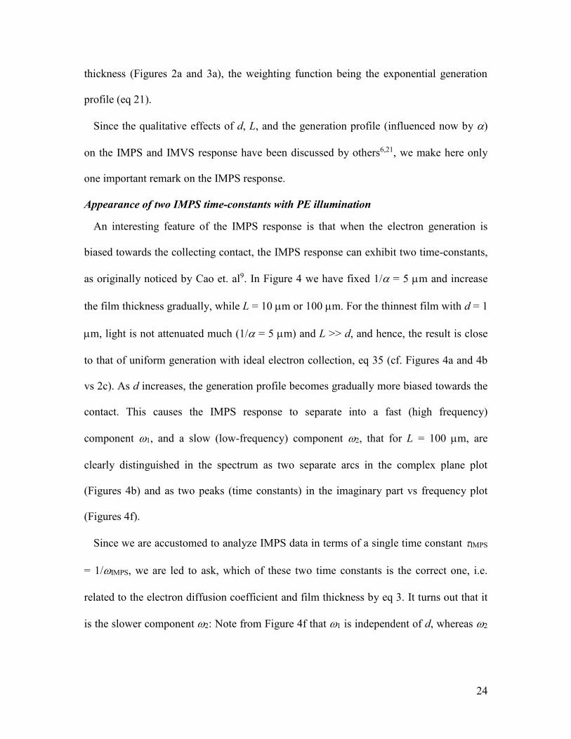
Figure 1. Geometry of the one-dimensional electron generation-collection problem with
exponential generation profiles. Two transport lengths can be distinguished when the
generation is strongly biased towards the collecting contact: 1. diffusion directly to the
contact, 2. diffusion to the opposite direction and reflection form the edge of the film.
Figure 2. Effect of film thickness (d) and locus of generation () on the IMPS spectra for
different cases of spatial electron generation. (a,d) localized generation at x = when d is
fixed to 30 m; (b,e) localized generation at the far edge of the film (x = = d); (c,f)
uniform generation. The arrows show the direction of increasing or d.
Figure 3. IMVS spectra for localized and uniform electron generation. See Figure 2 for
descriptions. The IMVS spectra are normalized by dividing each spectrum by the steady
state limit of the IMVS response for uniform illumination with the same and d (eq 38).
Figure 4. Effect of film thickness (d) on the IMPS spectra for exponential generation
profiles with fixed light penetration depth 1/ = 5 m and electron lifetime = 16 ms,
(2-1 = 10 Hz. Figures (a-d) show the complex plane plots and (e-h) the corresponding
imaginary component spectra, showing the effect of the illumination direction (PE- vs
CE-side) and electron diffusion length L (10 m vs 100 m). The arrows show the
direction of increasing d.
Figure 5. Effect of the film thickness and locus of generation on (a) IMPS time constant,
and (b) IMVS time constant. Three cases of exponential generation with PE illumination

39
(continuous lines) and CE illumination (dashed lines) with different light penetration
depth (1/) are shown in colors.
Figure 6. Effect of the film thickness and locus of generation on (a) relative electron
diffusion coefficient estimated by eq 3 using IMPS from Figure 5a, and (b) relative
electron diffusion length estimated by eq 2 using DEST and IMVS from Figures 5a and 5b.
Figure 7. Comparison of the photoelectrode thickness dependence of the IMPS time
constant for hypothetical, optically identical photoelectrode samples with equal but
different L. (a) Illumination from the photoelectrode side, (b) Illumination from the
counter electrode side, (c) uniform illumination.
Figure 8. Effect of the film thickness and locus of generation on the electron collection
efficiency. (a) The exact values by the diffusion model using D = 6.25·10-6 m2/s and =
16 ms (L = 10 m), and (b) errors introduced by estimating D = DEST (Figure 6a) and =
IMVS (Figure 5b). (c) Error introduced by using eq 4. (d) Minimum error corresponding
to fitting the complete IMPS spectrum, using a fixed estimated value = IMVS (Figure
5b).
Figure 9. Measured IMPS time constant as a function of film thickness in dye solar cells
having pressed TiO2 photoelectrode films with, or without, additional sintering at 450 °C.
40
Figure 1
41
Figure 2

42
Figure 3

43
Figure 4

44
Figure 5

45
Figure 6

46
Figure 7

47
Figure 7

48
Figure 9

49
References
(1) O'Regan, B.; Grätzel, M. Nature 1991, 353, 737-740.
(2) Peter, L. M. Phys. Chem. Chem. Phys. 2007, 9, 2630-2642.
(3) Ito, S.; Murakami, T. N.; Comte, P.; Liska, P.; Grätzel, C.; Nazeeruddin, M. K.;
Grätzel, M. Thin Solid Films 2008, 516, 4613-4619.
(4) Södergren, S.; Hagfeldt, A.; Olsson, J.; Lindquist, S. J. Phys. Chem. 1994, 98,
5552-5556.
(5) Halme, J.; Boschloo, G.; Hagfeldt, A.; Lund, P. J. Phys. Chem. C 2008, 112, 5623-
5637.
(6) Dloczik, L.; Ileperuma, O.; Lauermann, I.; Peter, L. M.; Ponomarev, E. A.;
Redmond, G.; Shaw, N. J.; Uhlendorf, I. J. Phys. Chem. B 1997, 101, 10281-10289.
(7) Franco, G.; Gehring, J.; Peter, L. M.; Ponomarev, E. A.; Uhlendorf, I. J. Phys.
Chem. B 1999, 103, 692-698.
(8) Schlichthörl, G.; Huang, S. Y.; Sprague, J.; Frank, A. J. J. Phys. Chem. B 1997,
101, 8141-8155.
(9) Cao, F.; Oskam, G.; Meyer, G. J.; Searson, P. C. J. Phys. Chem. 1996, 100, 17021-
17027.
(10) Fisher, A. C.; Peter, L. M.; Ponomarev, E. A.; Walker, A. B.; Wijayantha, K. G. U.
J. Phys. Chem. B 2000, 104, 949-958.

50
(11) Bisquert, J.; Vikhrenko, V. S. J. Phys. Chem. B 2004, 108, 2313-2322.
(12) van de Lagemaat, J.; Park, N. G.; Frank, A. J. J. Phys. Chem. B 2000, 104, 2044-
2052.
(13) Quintana, M.; Edvinsson, T.; Hagfeldt, A.; Boschloo, G. J. Phys. Chem. C 2007,
111, 1035-1041.
(14) Nakade, S.; Kubo, W.; Saito, Y.; Kanzaki, T.; Kitamura, T.; Wada, Y.; Yanagida,
S. J. Phys. Chem. B 2003, 107, 14244-14248.
(15) van de Lagemaat, J.; Frank, A. J. J. Phys. Chem. B 2001, 105, 11194-11205.
(16) Miettunen, K.; Halme, J.; Toivola, M.; Lund, P. J. Phys. Chem. C 2008, 112,
4011-4017.
(17) Peter, L. M.; Wijayantha, K. G. U. Electrochem. Comm. 1999, 1, 576-580.
(18) Schlichthörl, G.; Park, N. G.; Frank, A. J. J. Phys. Chem. B 1999, 103, 782-791.
(19) Trupke, T.; Wurfel, P.; Uhlendorf, I. J. Phys. Chem. B 2000, 104, 11484-11488.
(20) Bisquert, J. Phys. Chem. Chem. Phys. 2003, 5, 5360-5364.
(21) Peter, L. M.; Ponomarev, E. A.; Franco, G.; Shaw, N. J. Electrochim. Acta 1999,
45, 549-560.
(22) O'Regan, B. C.; Bakker, K.; Kroeze, J.; Smit, H.; Sommeling, P.; Durrant, J. R. J.
Phys. Chem. B 2006, 110, 17155-17160.

51
(23) Oekermann, T.; Zhang, D.; Yoshida, T.; Minoura, H. J. Phys. Chem. B 2004, 108,
2227-2235.
(24) Sinkkonen, J.; Ruokolainen, J.; Uotila, P.; Hovinen, A. Appl. Phys. Lett. 1995, 66,
206-208.
(25) Duffy, N. W.; Peter, L. M.; Rajapakse, R. M. G.; Wijayantha, K. G. U.
Electrochem. Comm. 2000, 2, 658-662.
(26) Bailes, M.; Cameron, P. J.; Lobato, K.; Peter, L. M. J. Phys. Chem. B 2005, 109,
15429-15435.
(27) Bisquert, J.; Garcia-Belmonte, G.; Fabregat-Santiago, F.; Ferriols, N. S.;
Bogdanoff, P.; Pereira, E. C. J. Phys. Chem. B 2000, 104, 2287-2298.
(28) Bay, L.; West, K. Solar Energy Mater. Solar Cells 2005, 87, 613-628.
(29) Macdonald, J. R.; Impedance spectroscopy: empasizing solid materials and
systems; Wiley: New York, 1987
(30) Duffy, N. W.; Peter, L. M.; Wijayantha, K. G. U. Electrochem. Comm. 2000, 2,
262-266.
(31) Van der Zanden, B.; Goossens, A. J. Phys. Chem. B 2000, 104, 7171-7178.
(32) de Jongh, P. E.; Vanmaekelbergh, D. J. Phys. Chem. B 1997, 101, 2716-2722.
(33) Cass, M. J.; Qiu, F. L.; Walker, A. B.; Fisher, A. C.; Peter, L. M. J. Phys. Chem. B
2003, 107, 113-119.

52
(34) Jennings, J. R.; Peter, L. M.; J. Phys. Chem. C 2007, 111, 16100-16104.
(35) Anta, J. A.; Casanueva, F.; Oskam, G. J. Phys. Chem. B 2006, 110, 5372-5378.
(36) Benkstein, K. D.; Kopidakis, N.; van de Lagemaat, J.; Frank, A. J. Mater. Res.
Soc. Symp. Proc. 2004, 789, 325-330.
(37) Nister, D.; Keis, K.; Lindquist, S.; Hagfeldt, A. Solar Energy Mater. Solar Cells
2002, 73, 411-423.


![Lund, P. D.; Halme, J.; Hashmi, G.; Asghar, I.; Miettunen ... · annum [MIT 2015, Harry 2017, REN21 2017]. But the future prospects for PV look even better, e.g. in some scenarios](https://static.fdocuments.us/doc/165x107/6047c3881a650d1923286d3e/lund-p-d-halme-j-hashmi-g-asghar-i-miettunen-annum-mit-2015-harry.jpg)