GUJARAT TECHNOLOGICAL UNIVERSITY - … its working with necessary waveforms. 07 OR Q.3 (a) Draw...
19
1 Seat No.: ________ Enrolment No.___________ GUJARAT TECHNOLOGICAL UNIVERSITY BE - SEMESTER–III • EXAMINATION – SUMMER 2013 Subject Code: 131101 Date: 31-05-2013 Subject Name: Basic Electronics Time: 02.30 pm - 05.00 pm Total Marks: 70 Instructions: 1. Attempt all questions. 2. Make suitable assumptions wherever necessary. 3. Figures to the right indicate full marks. Q.1 (a) Define electron volt and draw general energy band diagram for insulator, semiconductor, and metal. 07 (b) State Bohr’s postulates and derive expression for energy levels of electrons in Joules as a function orbit number surrounding nucleus. 07 Q.2 (a) Explain the term mobility related to charged carriers and derive expression for point form of Ohm’s law. 07 (b) Describe phenomenon of Hall effect with mathematical derivations. What are the different applications of Hall effect? 07 OR (b) Obtain expression for potential difference across a semiconductor with non- uniform (graded) doping. Using the same, derive an expression for potential difference across open-circuited step-graded p-n junction. 07 Q.3 (a) Define and explain following terms related to diode: 1. Transition capacitance and 2. Diffusion capacitance. 07 (b) Draw double-diode clipper circuit which limits output voltage at two independent levels. Explain its working with necessary waveforms. 07 OR Q.3 (a) Draw diode I-V characteristic and explain diode static and dynamic resistances. 07 (b) Explain working full-wave rectifier with necessary waveforms. Obtain expression for dc output voltage. 07 Q.4 (a) Indicate and briefly explain various current components flowing in p-n-p transistor with forward-based emitter junction and reverse-biased collector junction. 07 (b) Define h-parameters, and draw h-parameter equivalent circuit for CE, CB and CC configured transistor. 07 OR Q.4 (a) Draw output and input characteristics for common-base configured transistor. Explain base-width modulation (Early effect) for the same. 07 (b) Derive expression for small-signal voltage gain of emitter follower circuit in terms of h-parameters. 07 Q.5 (a) What do you understand by bias stability in transistor amplifier circuit? Explain thermal instability of bias point for the same. 07 (b) Draw structure of n-channel JFET and explain its working. 07 OR Q.5 (a) Draw and explain working of diode compensation circuit for V BE for self- stabilization in amplifier circuit. 07 (b) Compare FET and BJT devices. Define small-signal parameters of FET and draw low-frequency small-signal model for the same. 07 *************
Transcript of GUJARAT TECHNOLOGICAL UNIVERSITY - … its working with necessary waveforms. 07 OR Q.3 (a) Draw...

1
Seat No.: ________ Enrolment No.___________
GUJARAT TECHNOLOGICAL UNIVERSITY BE - SEMESTER–III • EXAMINATION – SUMMER 2013
Subject Code: 131101 Date: 31-05-2013 Subject Name: Basic Electronics Time: 02.30 pm - 05.00 pm Total Marks: 70 Instructions:
1. Attempt all questions. 2. Make suitable assumptions wherever necessary. 3. Figures to the right indicate full marks.
Q.1 (a) Define electron volt and draw general energy band diagram for insulator,
semiconductor, and metal. 07
(b) State Bohr’s postulates and derive expression for energy levels of electrons in Joules as a function orbit number surrounding nucleus.
07
Q.2 (a) Explain the term mobility related to charged carriers and derive expression for point form of Ohm’s law.
07
(b) Describe phenomenon of Hall effect with mathematical derivations. What are the different applications of Hall effect?
07
OR (b) Obtain expression for potential difference across a semiconductor with non-
uniform (graded) doping. Using the same, derive an expression for potential difference across open-circuited step-graded p-n junction.
07
Q.3 (a) Define and explain following terms related to diode: 1. Transition capacitance and 2. Diffusion capacitance.
07
(b) Draw double-diode clipper circuit which limits output voltage at two independent levels. Explain its working with necessary waveforms.
07
ORQ.3 (a) Draw diode I-V characteristic and explain diode static and dynamic
resistances. 07
(b) Explain working full-wave rectifier with necessary waveforms. Obtain expression for dc output voltage.
07
Q.4 (a) Indicate and briefly explain various current components flowing in p-n-p
transistor with forward-based emitter junction and reverse-biased collector junction.
07
(b) Define h-parameters, and draw h-parameter equivalent circuit for CE, CB and CC configured transistor.
07
OR Q.4 (a) Draw output and input characteristics for common-base configured transistor.
Explain base-width modulation (Early effect) for the same. 07
(b) Derive expression for small-signal voltage gain of emitter follower circuit in terms of h-parameters.
07
Q.5 (a) What do you understand by bias stability in transistor amplifier circuit?
Explain thermal instability of bias point for the same. 07
(b) Draw structure of n-channel JFET and explain its working. 07 OR
Q.5 (a) Draw and explain working of diode compensation circuit for VBE for self-stabilization in amplifier circuit.
07
(b) Compare FET and BJT devices. Define small-signal parameters of FET and draw low-frequency small-signal model for the same.
07
*************

1
Seat No.: _____ Enrolment No.______
GUJARAT TECHNOLOGICAL UNIVERSITY B.E. Sem-III Examination December 2009
Subject code: 131101 Subject ame: Basic Electronics Date: 17 /12 / 2009 Time: 11.00 am – 1.30 pm
Total Marks: 70
Instructions: 1. Attempt all questions.
2. Make suitable assumptions wherever necessary.
3. Figures to the right indicate full marks.
Q.1 (a) Define following terms:
(i) Electron Volt (eV).
04
(ii) Mobility of charge carries.
(iii) Barrier potential.
(iv) Voltage equivalent of temperature.
(b) Explain energy band diagram of insulator, semiconductor and
conductor.
05
(c) Explain following for npn transistor. 05
(i) Current components.
(ii) Regions of operation according to biasing condition
Q.2 (a) Draw the circuit diagram of full wave bridge rectifier and give its input
and output waveforms. Also derive the expression for the d.c. current.
07
(b) Explain Hall effect. Derive expression of Hall voltage and state its
applications.
07
OR
(b) A bar of n type silicon has length of 5 cm and circular cross sectional
area of 10 mm2. When it is subjected to a voltage of 1 V along its
length, the current flowing through it is 5 mA. Calculate the
concentration of free electrons and drift velocity of electrons. Assume
mobility of free electrons to be 1300 cm2/V-s.
07
Q.3 (a) Compare zener and avalanche break down. 04
(b) What is transition capacitance in p-n junction diode? Give its physical
significance.
05
(c) State the use of clipping circuits. Discuss with neat sketch working of a
biased parallel clipper.
05
OR
Q.3 (a) Explain principle of operation of a Photodiode. 04
(b) Discuss piece-wise linear model of a diode. 05
(c) Compare V-I characteristics of Silicon and Germanium p-n junction
diode.
05
Q.4 (a) Draw CE transistor configuration and give its input and output
characteristics. Also derive the relation between current gain of CE,
CB and CC configurations.
07
(b) Give constructional details of JFET and give its characteristics. Why
FET is called voltage controlled device?
07
OR

2
Q.4 (a) Explain the operation of Emitter follower amplifier. Why is it named as
emitter follower?
07
(b) Give points of difference between BJT and FET. Also explain FET as
voltage variable resistor.
07
Q.5 (a) State the need of biasing. Discuss voltage divider bias circuit and
mention its advantages.
07
(b) What is the difference between voltage amplifier and power amplifier?
State important features of power amplifier and classify them based on
the position of Q point.
07
OR
Q.5 (a) Discuss h-parameter equivalent circuit for transistor in CE
configuration.
07
(b) State the role of voltage regulators in power supplies? Discuss working
of a series voltage regulator.
07
***********
1
Seat No.: _____ Enrolment No.______
GUJARAT TECHNOLOGICAL UNIVERSITY B.E. Sem-III Remedial Examination March 2010
Subject code: 131101
Subject ame: Basic Electronics
Date: 09 / 03 / 2010 Time: 3.00 pm – 05.30 pm
Total Marks: 70
Instructions: 1. Attempt all questions.
2. Make suitable assumptions wherever necessary.
3. Figures to the right indicate full marks.
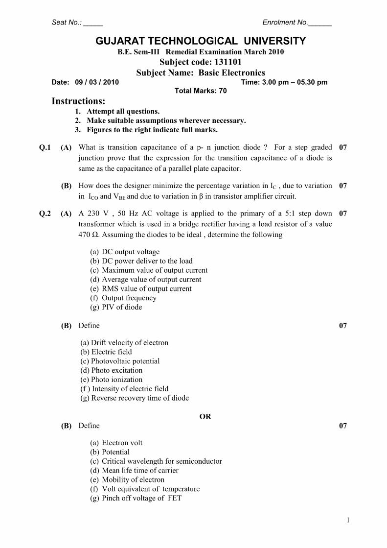
Q.1 (A) What is transition capacitance of a p- n junction diode ? For a step graded
junction prove that the expression for the transition capacitance of a diode is
same as the capacitance of a parallel plate capacitor.
07
(B) How does the designer minimize the percentage variation in IC , due to variation
in ICO and VBE and due to variation in β in transistor amplifier circuit.
07
Q.2 (A) A 230 V , 50 Hz AC voltage is applied to the primary of a 5:1 step down
transformer which is used in a bridge rectifier having a load resistor of a value
470 Ω. Assuming the diodes to be ideal , determine the following
(a) DC output voltage
(b) DC power deliver to the load
(c) Maximum value of output current
(d) Average value of output current
(e) RMS value of output current
(f) Output frequency
(g) PIV of diode
07
(B) Define
(a) Drift velocity of electron
(b) Electric field
(c) Photovoltaic potential
(d) Photo excitation
(e) Photo ionization
(f ) Intensity of electric field
(g) Reverse recovery time of diode
07
OR
(B) Define
(a) Electron volt
(b) Potential
(c) Critical wavelength for semiconductor
(d) Mean life time of carrier
(e) Mobility of electron
(f) Volt equivalent of temperature
(g) Pinch off voltage of FET
07

2
Q.3 (A) A bar of silicon 0.2 cm long has a cross sectional area of 9 × 10⁻⁸
m2 , heavily
doped with phosphorus. What will be the majority carrier density resulting from
doping if the bar is to have resistance of 2 kΩ ? Given for silicon at room
temperature :
µn= 0.14 m2/V-sec, µp= 0.05 m
2/V-sec, ni= 1.5 × 10
10 /cm
3, q =1.602 ×10
-19 C
04
(B) Give minimum four comparisons of following semiconductor devices
(1) Tunnel diode with conventional diode.
(2) LED with conventional diode.
(3) LED with photo diode.
06
(C) Prove that current density is proportional to product of charge density , mobility
of charge and electric field intensity.
04
OR
Q.3 (A) A static resistance of 4 Ω is observed in an ideal germanium diode at room
temperature. The current flowing through the diode is 50mA. If the forward
biased voltage is 0.2V , volt equivalent temperature is 26mV , calculate :
(i) Reverse saturation current
(ii) Dynamic resistance of diode
04
(B) Draw output waveform of following circuits. Consider input of 20V (peak to
peak), 10kHz sine wave and assume ideal diode.
(i)
1kΩ
V1
5 V
Vi Vo
+
__
+
(ii)
1kΩ
5 V
Vi Vo
_
++
_
1µF
06
(C) Explain the hall effect in semiconductor. How hall effect is considered in
measurement of mobility and conductivity?
04
Q.4 (A) Derive relationship between αdc and βdc of a transistor. 04
(B) Explain any one circuit which is used to improve the input impedance of the
amplifier.
06
3
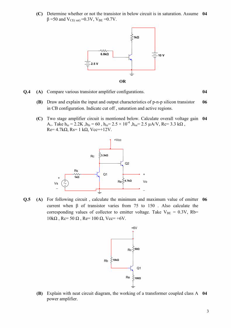
(C) Determine whether or not the transistor in below circuit is in saturation. Assume
β =50 and VCE( sat) =0.3V, VBE =0.7V.
10 V 6.8kΩ
1kΩ
2.5 V
04
OR
Q.4 (A) Compare various transistor amplifier configurations. 04
(B) Draw and explain the input and output characteristics of p-n-p silicon transistor
in CB configuration. Indicate cut off , saturation and active regions.
06
(C) Two stage amplifier circuit is mentioned below. Calculate overall voltage gain
Av. Take hie = 2.2K ,hfe = 60 , hre= 2.5 × 10⁻⁴
,hoe= 2.5 µA/V, Rc= 3.3 kΩ ,
Re= 4.7kΩ, Rs= 1 kΩ, Vcc=+12V.
1kΩ
3.3kΩ
4.7kΩ
+
_
Vo
+Vcc
+
_Vs
Rs
Rc
Re
Q1
Q2
04
Q.5 (A) For following circuit , calculate the minimum and maximum value of emitter
current when β of transistor varies from 75 to 150 . Also calculate the
corresponding values of collector to emitter voltage. Take VBE = 0.3V, Rb=
10kΩ , Rc= 50 Ω , Re= 100 Ω, Vcc= +6V.
10kΩ
50Ω
100Ω
+6V
Rb
Rc
Re
Q1
06
(B) Explain with neat circuit diagram, the working of a transformer coupled class A
power amplifier.
04
4
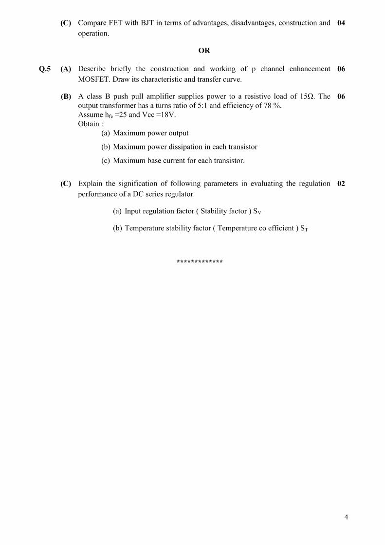
(C) Compare FET with BJT in terms of advantages, disadvantages, construction and
operation.
04
OR
Q.5 (A) Describe briefly the construction and working of p channel enhancement
MOSFET. Draw its characteristic and transfer curve.
06
(B) A class B push pull amplifier supplies power to a resistive load of 15Ω. The
output transformer has a turns ratio of 5:1 and efficiency of 78 %.
Assume hfe =25 and Vcc =18V.
Obtain :
(a) Maximum power output
(b) Maximum power dissipation in each transistor
(c) Maximum base current for each transistor.
06
(C) Explain the signification of following parameters in evaluating the regulation
performance of a DC series regulator
(a) Input regulation factor ( Stability factor ) SV
(b) Temperature stability factor ( Temperature co efficient ) ST
02
*************

1
Seat No.: _____ Enrolment No.______
GUJARAT TECHNOLOGICAL UNIVERSITY B.E. Sem-III Regular / Remedial Examination December 2010
Subject code: 131101
Subject Name: Basic Electronics Date: 13 /12 /2010 Time: 10.30 am – 01.00 pm
Total Marks: 70
Instructions: 1. Attempt all questions. 2. Make suitable assumptions wherever necessary. 3. Figures to the right indicate full marks.
Q.1 (a) Answer the following:
(i) What is semiconductor? Define a hole in semiconductor
(ii) State the Pauli exclusion principle
(iii) Sketch the piecewise linear characteristics of p-n diode
(iv ) Define an electron volt (eV)
(v) State the mass-action law as an equation and in word.
(vi) What is cutin voltage? Write approx. value of cutin voltage for silicon
and germanium diode
(vii) Write the equation for the volt-ampere characteristic a photo diode
07
(b) Draw and explain bridge rectifier circuit with capacitorfilter. Draw necessary
waveforms. 07
Q.2 (a) Draw the circuit of CE configuration of transistor. ExplainInput and output
characteristics. Derive α = β / β+1 07
(b) (i) Draw symbol and explain briefly the working principle Breakdown diode and
Tunnel diode 04
(ii)Write principle and applications of light emitting diode 03
OR
(b) (i) Describe the Hall effect. Which properties of a Semiconductor are
determined from Hall effect experiment? 04
(ii) Explain electrical properties of germanium and silicon ( conductivity ,the
mobility and the energy gape) 03
Q.3 (a) Draw following diode circuits with input and output Waveforms:
(i) Voltage doublers circuit 03
(ii) Positive clipping circuit 02
(iii) Negative clamper circuit 02
(b) (i) A 5kΩ load is fed from a bridge rectifier connected with a transformer
secondary whose primary is connected to 460V, 50 Hz supply. The ratio of
number of primary to secondary turns is 2 : 1. Calculate dc load current ,dc
load voltage , ripple voltage and PIV rating of diode,
04
(ii) A 100µF capacitor when used as a filter has 12 V dc Across it with a terminal
load resistor of 2.5kΩ. If the rectifier is full wave and supply frequency is 50
Hz calculate the percentage of ripple in the output
03
OR
Q.3 (a) Explain the h-parameter model of CE amplifier with Bypass resistor RE and
derive the expression for Ai , Av , Ri , Ro 07
(b) Find hre in terms of the CB h-parameters 07

2
Q.4 (a) What is biasing? Why biasing is required for transistor? List biasing methods for
transistor. Draw and explain the circuit of voltage divider biasing 07
(b) Where CC configuration is used? Draw circuit of CC and CB configuration of
transistor. Compare current gain ,voltage gain ,input impedance and output
impedance of both
07
OR
Q.4 (a) A CE amplifier using npn transistor has load resistance RL connected between
collector and Vcc supply of + 16 V For biasing resistor , R1 is connected between
Vcc and base Resistor R2 = 30 kΩ is connected between base and ground. RE =
1kΩ. Draw the circuit diagram and calculate the value of R1 , RC ,stability factor
S if VBE = 0.2V, IEQ = 2 mA , VCEQ = 6 V , α = 0.985
07
(b) Design a fixed bias circuit using silicon npn transistor Which has βdc = 150. The
dc biasing point is VCE = 5V And Ic = 5 mA Supply voltage is 10V.Write
advantages and disadvantages of fixed bias circuit.
07
Q.5 (a) (i) Define the pinch-off voltage Vp .Sketch the depletion region before and after
pinch-off. 03
(ii) Sketch the cross section of a P-channel enhancement MOSFET .Show two
circuit symbol for MOSFET 04
(b) Draw circuit of an idealized class-B push-pull power amplifier and explain its
operation with the help of necessary waveforms. 07
OR
Q.5 (a) (i) Compare different types of power amplifier based on conduction angle ,
position of Q-point , efficiency and distortion 04
(ii) Draw circuit of transistor as a switch 03
(b) A MOSFET has a drain- circuit resistance Rd of 100K and operates at 20 kHz.
The MOSFET parameters are gm = 1.6 mA/V, rd = 44K , Cgs = 3 Pf Cds = 1 pF
,Cgd = 2.8 pF.Calculate the voltage gain of this device .
07
*************

1
Seat No.: _____ Enrolment No.______
GUJARAT TECHNOLOGICAL UNIVERSITY B.E. Sem-III Examination May 2011
Subject code: 131101 Subject Name: Basic Electronics Date:30/05/2011 Time: 10.30am to 1.00pm
Total Marks: 70
Instructions: 1. Attempt all questions.
2. Make suitable assumptions wherever necessary.
3. Figures to the right indicate full marks.
Q.1 (a) Prove that the minority carrier concentration, in an n-type semiconductor bar which was momentarily illuminated, decreases exponentially with time.
07
(b) Derive continuity equation and explain its importance. 07
Q.2 (a) When a diode is driven from forward condition to reverse condition, draw and explain waveforms for (1) minority carrier concentration at the junction of the diode (2) current flowing through the diode circuit, and (3) voltage across the diode. Assume resistance (RL) is present in series with diode.
07
(b) A symmetrical 5-kHz square wave whose output varies between +10 V and -10 V is impressed upon the clipping circuit shown in Fig. 1. Assume diode forward resistance (Rf) as zero, diode reverse resistance as (Rr) 2M, diode cut-in voltage (Vγ) as zero. Sketch the steady-state output waveform, indicating numerical values of the maximum, minimum, and constant portions.
07
OR
(b) Design a Zener regulator (Fig. 2) for following specifications: load current IL = 20 mA, output voltage Vo = 5 V, Zener wattage PZ = 500 mW, Input voltage Vi = 12 ± 2 V, and IZ,(min) = 8 mA,
07
Q.3 (a) A silicon transistor with VBE, sat = 0.8 V, β = hFE = 100, VCE, sat = 0.2 V is used in the circuit shown in Fig. 3. Find the minimum value of RC for which the transistor remains in saturation.
07
(b) Derive expressions for AI, Ri, AV, and Yo in terms of CE h-parameters for emitter-follower circuit.
07
OR
Q.3 (a) Represent/derive CC h-parameters (hic and hfc) in terms of CE h-parameters . 07
(b) Explain the base-width modulation and its effect on minority-carrier concentration in the base region of a transistor as well as on the common-base input characteristics of a typical p-n-p transistor.
07
Q.4 (a) Define stabilization factors: S, S’, and S”. Derive expressions for S and S’ for self-bias transistor circuit.
07
(b) Derive an expression for voltage gain (AV) for CS amplifier with an bypassed source resistance RS.
07
OR
Q.4 (a) The fixed-bias circuit is given in Fig. 4 and it is subjected to an increase in
temperature from 25 C to 75 C. If β = 100 at 25 C and β = 125 at 75 C,
determine the percentage change in Q point values (VCE, IC) over the temperature range. Neglect any change in VBE. Take VBE = 0.7 V.
07

2
(b) Draw a structure of p-channel MOSFET. Explain its working for enhancement type. Also draw and explain drain characteristics and transfer curve for the same device.
07
Q.5 (a) Illustrate how the energy levels of isolated atoms in group IV A (e.g., C, Si, Ge, Sn) are split into energy bands when these atoms are brought into close proximity to form a crystal. Draw necessary energy band diagrams.
07
(b) Show that the upper limit of the conversion efficiency (η) for the series-fed class A amplifier is 25 %.
07
OR
Q.5 (a) Draw class B push-pull system and show that the maximum conversion efficiency (η) is 78.5 % for this system.
07
(b) Draw and explain working of the circuit for compensation of VBE using diode. 07
2.5 V
1 MVi Vo
Figure 1 Q:2 (b)
I L
IZR
RLVi
I
Vo
+
−
+
Figure 2 Q:2 (b) OR
10 V
5 V
200 K
Rc
Figure 3 Q:3 (a)
RBI
R
IB
C
C
100 KOhm
600 Ohm
12 V
Figure 4 Q:4(a) OR
*************

1
Seat No.: _________ Enrolment No._______________
GUJARAT TECHNOLOGICAL UNIVERSITY BE SEM-III Examination-Dec.-2011
Subject code: 131101 Date: 20/12/2011
Subject Name: Basic Electronics
Time: 2.30 pm -5.00 pm Total marks: 70 Instructions:
1. Attempt all questions.
2. Make suitable assumptions wherever necessary.
3. Figures to the right indicate full marks.
Q.1 (a) Explain the concept of potential energy barrier. 07
(b) State the limitations of Rutherford model and explain Bohr atomic
model.
07
Q.2 (a) Explain the mobility and conductivity using electron-gas theory. Also
derive the expression of current density.
07
(b) Describe the Hall effect and also explain how it is help to determine
the different properties of semiconducting material.
07
OR
(b) Explain the generation of holes and electrons in an intrinsic
semiconductor.
07
Q.3 (a) Explain the formation of barrier potential in open circuited PN
junction diode. Also derive the expression for barrier potential.
07
(b) A diode having internal resistance 20Ω is used for half-wave
rectification. If the applied voltage V=50sin(ωt) and load resistance
RL=800Ω,find:
1) Im, Idc, Irms
2) d.c. output voltage
3) efficiency of rectification.
07
OR
Q.3 (a) Define the rectification and describe the full wave bridge rectifier with
the help of neat circuit diagram and waveforms.
07
(b) The resistivities of two sides of a step graded germanium diode are 2
Ω.cm and 1 Ω.cm for p-side and n-side respectively. Calculate the
height of potential energy barrier Vo. Assume µp=1800 cm2/v.sec,
µn=2100 cm2/v.sec, q=1.6×10
-19 ni= 2.5 ×10
13 per cm
3
07
Q.4 (a) Define following terms:
1) PIV
2) voltage equivalent of temperature
3) electric potential
4) electron volt
5) Ripple factor
6) base spreading resistance
7) pinch off voltage
07
(b) Explain the different types of clipping circuits. 07 OR

2
Q.4 (a) Explain the output characteristic of n-p-n transistor in CE
configuration. Also indicate different regions.
07
(b) Determine h-parameters for the two port network. Also draw the
hybrid model for CE, CB and CC configurations.
07
Q.5 (a) Explain DC load line and Q-point for any transistor configuration.
Also state the necessity of biasing and list biasing methods for
transistor.
07
(b) List the basic configurations of a low frequency FET amplifier.
Explain any one of them with the help of neat circuit diagram and
small signal equivalent circuit.
07
OR
Q.5 (a) Classify the power amplifiers based on the position of Q-point on the
ac load line. Also explain Class-B push-pull amplifier.
07
(b) Explain the principle of operation of JFET. Also compare FET with
BJT.
07
*************

1
Seat No.: _____ Enrolment No.______
GUJARAT TECHNOLOGICAL UNIVERSITY BE SEM-III Examination May 2012
Subject code: 131101 Subject Name: Basic Electronics
Date: 11/05/2012 Time: 02.30 pm – 05.00 pm Total Marks: 70 Instructions:
1. Attempt all questions. 2. Make suitable assumptions wherever necessary. 3. Figures to the right indicate full marks.
Q.1 (a) Define the following terms: [7]
(i) Potential (ii) ev unit of energy (iii) Volt-equivalent temperature (iv) Thermal resistance (v) Intermodulation distortion (vi) Mean life time of a carrier (vii) Peak Inverse Voltage
(b) Draw and explain the transistor current components when it is biased in active region. Obtain the generalized transistor equation.
[5]
(c) In n-type semiconductor, concentration of donor atoms is 4.14×10¹⁴ atoms/cm3. Calculate the conductivity and resistivity of semiconductor. (Assume: mobility of electron=3800 cm2/volt.sec)
[2]
Q.2 (a) Explain the Hall effect and obtain the expression of Hall coefficient. List the
applications of Hall effect. [5]
(b) Explain the concept of potential barrier and state Bohr’s postulates. [5] (c) Draw the circuit of sampling gate and explain its operation. [4]
OR (c) A germanium diode has a contact potential of 0.2v, while the concentration of
acceptor impurity atoms is 3×10²⁰ per m3, calculate for a reverse bias of 0.1v, the width of the depletion region. If the reverse bias is increased to 10v, calculate the new width of the depletion region. Assuming cross-sectional area of the junction as 1mm2, calculate the transition capacitance values for both cases. Assume Er as 16 for germanium.
[4]
Q.3 (a) Draw circuit of CB transistor and explain its input and output characteristics. [5] (b) Figure No. 1 shows the two way clipper. If the input voltage is sinusoidal source of
16v peak-to-peak, sketch the output waveform. (Assume voltage drop across diodes is 0.7v)
[5]
(c) Sketch the full-wave rectifier circuit and explain its operation. [4] OR

2
Q.3 (a) Verify mathematically that transistor means “transfer resistor”. Explain the working
of phototransistor.
[5]
(b) Figure No. 2 shows an n-p-n transistor. It has the Ico= 2×10⁻⁵mA and β=100. Find the transistor currents and value of α of transistor.
[5]
(c) Distinguish: (i) avalanche breakdown and Zener breakdown. [4] (ii) Drift current and diffusion current.
Q.4 (a) Draw the self-bias circuit and explain how it establishes the stable operating point. [5] (b) Draw push-pull arrangement of two transistors and prove that this arrangement can
balance out all even harmonics. [5]
(c) Define thermal runaway. Derive necessary condition to avoid thermal runaway. [4] OR
Q.4 (a) Explain the operation of class A large signal amplifier with circuits and output
waveforms and also derive the expression of output power. [5]
(b) Check the condition to avoid the thermal runaway of a self bias circuit, if Vcc=30v, Rc= 2.0KΩ, Re= 4.7KΩ and collector current Ic=1.5mA and give the comments. (Assume that collector current increases by 0.131mA over temperature range of 25 to 75oC).
[5]
(c) Draw and explain regulated power supply system. [4]
Q.5 (a) Draw following circuits:
(i) Small-signal high frequency equivalent common drain FET amplifier. (ii) Ebers-Moll model of P-N-P transistor.
[6]
(b) Explain the working and characteristics of p-channel enhancement type MOSFET. [5] (c) Datasheet for a JFET indicates that IDSS=10mA and VGS(off) = -4v. Determine the
drain current for VGS= 0v, -1v. [3]
OR Q.5 (a) Draw a transistor amplifier circuit using h parameter and derive expressions for
current gain, voltage gain, input impedance and output impedance. [6]
(b) Consider a single stage CE amplifier (Figure No. 3) with Rs=1KΩ, R1=50KΩ, R2= 2KΩ, Rc= 1KΩ, RL= 1.2KΩ, hfe= 50, hie=1.1KΩ, hoe= 25 µA/V and hre= 2.5×10⁻⁴. Find current gain, input resistance, voltage gain and output resistance.
[5]
(c) Draw the circuit of emitter follower. [3]

3
Figure No. - 1
Vo

4
Figure No. - 2
Figure No. - 3
Rc
Rb

Seat No.: ________ Enrolment No.___________
GUJARAT TECHNOLOGICAL UNIVERSITY B. E. - SEMESTER – III • EXAMINATION – WINTER 2012
Subject code: 131101 Date: 07-01-2013 Subject Name: Basic Electronics Time: 10.30 am – 01.00 pm Total Marks: 70 Instructions:
1. Attempt all questions. 2. Make suitable assumptions wherever necessary. 3. Figures to the right indicate full marks.
Q.1 (a) Explain followings:
(i) Electron volt. (ii) Mobility (iii) Barrier potential (iv) Diffusion current (v) Mean life time of a carrier (vi) Graded semiconductor (vii) Intrinsic concentration
07
(b) Explain Hall effect with neat sketch. Discuss how to measure charge density and mobility for a given specimen of semiconductor using Hall Effect?
07
Q.2 (a) Specimen of material is 5 cm long and having radius of 5 mm. Current is
due to electrons whose mobility is 5000 cm2/V.s. Current of 50 mA flows through it when 0.5 Volt is impressed across it. Calculate concentration of free electrons and drift velocity.
07
(b) Explain potential variation in graded semiconductor. 07 OR (b) Derive the flowing equation for current density.
μεnqJ = 07
Q.3 (a) (i) Describe two breakdown mechanisms in a p-n junction diode.
(ii) Why the name varicap is given to varactor diode? Give its two applications.
04 03
(b) A sinusoidal voltage peak value of 10V and frequency 50 Hz is applied at the input of clipping circuit shown in figure below. Draw output voltage waveform and transfer characteristic. Assume both diodes are ideal.
07
OR
1

Q.3 (a) (i) Draw symbol of tunnel diode, Draw VI characteristic of tunnel diode and explain it.
(ii) Explain how Zener diode regulates voltage.
04 03
(b) A sinusoidal voltage peak value of 40V and frequency 50 Hz is applied at the input of a half wave rectifier, No filter is used. The Load resistance is 500 Ω. Neglect cut-in voltage. Diode has Rf = 5 Ω and Rr = . ∞(i) Draw Output voltage waveform and derive expression for DC output
voltage. (ii) Calculate DC value of load current, rms value of load current and
Rectification efficiency.
07
Q.4 (a) (i) Derive relation between α and ß for a transistor.
(ii) Why CE configuration is preferred for amplification? 04 03
(b) Draw a fixed bias circuit. State advantages and disadvantages of fixed bias circuit. Specify components value to have operating point at (9V, 2mA). Take VCC = 12 V and ß = 70.
07
OR Q.4 (a) (i) In npn transistor α = 0.98, IE = 20 mA, ICBO = 3µA. Determine IC, IB, ß
and ICEO (ii) What is early effect in CB configuration? Explain with graph.
04 03
Q.4 (b) Draw collector to base bias circuit and explain its operation. Also state advantages and disadvantages of the circuit.
07
Q.5 (a) Draw Emitter follower circuit. Obtain Hybrid equivalent circuit and derive
expression for current gain. 07
(b) (i) Does thermal runaway take place in FET? Why? (ii) Define parameters of FET and state relationship among them.
03 04
OR Q.5 (a) Determine Av, Ai, Ri and Ro for a common emitter amplifier using a
transistor with hie = 1200 Ω, hfe = 36, hre = 0 and hoe = 2 × 10⁻⁶ mho. Use RL = 2.5 K Ω, RS = 500 Ω and neglect the effect of biasing circuit.
07
(b) (i) Explain in what respect a power amplifier differ from a voltage amplifier?
(ii) Prove that the maximum theoretical collector circuit efficiency of a class A amplifier is 50%
03 04
*************
2