
Guide ISE14 - HAW Startseite: HAW Hamburg 1. Create a Project 3 2. Select a Device 4 3. Add the...
12
Guide ISE1 4 ISE 14.2 (Xilinx) Designflow 1/12
Transcript of Guide ISE14 - HAW Startseite: HAW Hamburg 1. Create a Project 3 2. Select a Device 4 3. Add the...

Guide ISE1 4
ISE 14.2 (Xilinx)
Designflow
1/12

Inhaltsverzeichnis
1. Create a Project 3
2. Select a Device 4
3. Add the Sourcecodes 5
4. File for the Pinning 6
5. Synthesis 7
6. Implementation 8
7. Programming of the Device 9
8. Generation of the Timesim-files 11
2/12

Start ISE13.4 from Desktop :
1. Create a Project
A new project (Projectfolder, projectfile ~.xise) will be created with:
→ File → New Project The menue „New Project Wizard“ arises:
The only one input is the name of the project.
Take care that
no special signs (except underscore),
no spaces,
no 'umlaut' und
not more than 20 signs
are used.
The lines „Location“ and „Working Directory“, the inserted path should read
„D:\ISE_Projects\<given projectname>“.
A subfolder of the project will be created.
Line „Top-level source type“ remains on „HDL“ .
Go on with click on
The select menue for the device starts automatically.
3/12

2. Select a Device
In the following menue „New Project Wizard“s select the device:
Go on with click on
The next menue „Project Summary“ shows all done settings..
Go on with click on
List of the used devices of our boards in our lab:
Family Device Package Speed
CPLD ModSys Coolrunner2 CPLDs XC2C256 PQ208 - 7
FPGA ModSys Spartan3E XC3S500E PQ208 - 5
ML507 Board Virtex5 XC5FX70T FF1136 - 1
NEXYS-II-Board Spartan3S1200E XC3S1200E FG320 - 4
CPLD (alt) XC9500 CPLDs XC9572 PC44 - 10
CPLD (alt) XC9500 CPLDs XC95108 PC84 - 7
Zed-Board Zynq XC72020 CLG484 - 1
EDK-Board (nur unter ISE10 !!) (Virtex2) (XC2VP30) (FF896) - 15
4/12

3. Add the Sourcecodes
→ Project → Add Source
Open the Windows-Open-Menue with: → Project → Add source
All necessary files (~.vhd, +.ucf) can be marked together and added at one time.
The following information menue „Adding source Files“ remains as it is and quit with:
The „Design“ → „Hierarchy“-field now contents:
First line Project name Second line: Device type
Third line : Entity name, Architecture name, File name Following lines: eventually components and the constraints-file ~.ucf:
In order to see the source code in the editor of ISE double click the filename in the list of hierarchy with the left button. The same with ucf-file.
or with marked UCF-File writung one time click with left mousebutton in field :„Processes“ → on „User Constraints“ → Edit Constraints (Text) .
In order to change the project settings later on double click left mouse button on „Design Properties“ of „Hierarchy“ window.
5/12
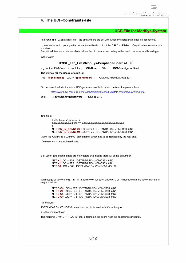
4. The UCF-Constraints-File
UCF-File for ModSys-System
In a UCF-file ( „Constraints“-file) the pinnumbers are set with which the portsignals shall be connected.
It determines which portsignal is connected with witch pin of the CPLD or FPGA. Only fixed connections are possible.
Predefined files are available which deliver the pin number according to the used connector and board-type
in the folder:
D:\ISE_Lab_Files\ModSys-Peripherie-Boards-UCF\
e.g. for the IOM-Board in subfolder IOM-Board File: IOM-Board_conn3.ucf
The Syntax for the usage of a pin is:
NET [signal-name] LOC = P[pin-number] | IOSTANDARD=LVCMOS33;
On our download site there is a UCF-generator available, which delivers the pin numbers:
http://www.haw-hamburg.de/ti-ie/labore/digitaltechnik-digitale-systeme/download.html
See: → 3. Entwicklungshardware → 3.1.1 to 3.1.3
Example:
#IOM Board Connector 3############## INPUTS ############################## #NET IOM_IN_CONN3<0> LOC = P76 | IOSTANDARD=LVCMOS33; #IN0NET IOM_IN_CONN3<1> LOC = P75 | IOSTANDARD=LVCMOS33; #IN1
„IOM_IN_CONN“ is a „Dummy“-signalname, which has to be replaced by the real one..
Delete or comment not used pins.
E.g. „exor“ (the used signals are not vectors this means there wil be no bitnumber ) :
NET X1 LOC = P76 | IOSTANDARD=LVCMOS33; #IN0NET X2 LOC = P75 | IOSTANDARD=LVCMOS33; #IN1NET Q1 LOC = P80 | IOSTANDARD=LVCMOS33; #OUT0
With usage of vectors e.g. D : in (3 downto 0) for each singe bit a pin is needed with the vector number in angle brackets:
NET D<0> LOC = P76 | IOSTANDARD=LVCMOS33; #IN0NET D<1> LOC = P75 | IOSTANDARD=LVCMOS33; #IN1NET D<2> LOC = P74 | IOSTANDARD=LVCMOS33; #IN2NET D<3> LOC = P73 | IOSTANDARD=LVCMOS33; #IN3
Annotation:
IOSTANDARD=LVCMOS33 says that the pin is used in 3,3 V technique.
# is the comment sign.
The marking „IN0“, „IN1“, „OUT0“ etc. is found on the board near the according connector.
6/12

5. Synthesation→ Synthesize-XST
The line of the Top-Level-Entity in window „Design Hierarchy“ must be marked by a right mouse click:
Then the action lines in field „Processes“ show up:
With double-left mouse-click on action line → Implement Design → Synthesize -XST the synthesation of the VHDL-source code starts.
Now the VHDL-code will be transposed to the available logic symbols. The constraints file(UCF) has no effect here.. The actual actions of „ISE“ are listed in the „Console“- window, also „ERROR“ and WARNING messages. In the windows below the tab „Errors“ or „Warnings“ these messages are collected.
Then the errors have to be corrected in the source code and the warnings have to be checked if they show a serious background. It only is senseful to begin with one up to three error messages on top.
Then start the synthesis anew. Repeat these actions until the following message in the console windowsappears:
Process "Synthesize - XST" completed successfully
The transposed design can be seen with click on:
→ Synthese → View RTL Schematic :
Quit the incidential menue „ Start with a schematic … „ with :
The the top level block schemtic appears e.g. :
The gate level will be shown by clicking with left mouse button on the box again and again until the lowest level is reached.
With the button:
w
The whole schematic is shown.
A white background is achieved with: → Edit → Preferences → RTL/Technology Viewers → Color Scheme
7/12

6. Implementation→ Implement Design
If not previously done the UCF constraint file must be created and added to the project.
Reminiscence:
It is an ASCII-file wich can be written in a normal texteditor. An example line is:
NET IOM_IN_CONN3<0> LOC = P76 | IOSTANDARD=LVCMOS33; #IN0
The dummy name IOM_IN_CONN3<0> has to be replaced by the real signal name. All signals in the portlist have to be connected to a pin in a statementline as above. The file has to be added to the project as decribed in point 3 with:
→ Project → Add source It should be listed below the top entity line in the design window. (Click on the + sign in front .)
Then mark the top-level-entity in field design Hierarchy :
Until then the action lines in the field „Processes“ become visible:
Double click with left mouse button on the action line „Implement Design“ starts the implementation.Now the subtopics „Translate“, „Fit“ and with CPLDs „Generate Programming File“ are executed.Error messages can be read in the console window with active tab „Errors“. Now mostly the arising errors can only concern the UCF-file or the wrong device has been chosen. (See chapter 2 ending)
Correct errors and execute implementation until there are no errors. Now check also the warnings. They can be seen in the „Console“-window with activ tab „Warnings“:
This warning which occurs on CPLD's is without concern: WARNING:Cpld – Unable to retrieve the path to the iSE Project Repository.
Will use the default filename of 'EXOR.ise'.
Also following warning can be ignored:Cpld - Inferring BUFG constraint for signal 'CLK' based upon the LOC constraint 'P55'. It is recommended that you declare this BUFG explicitedly in your design. Note that for certain device families the output of a BUFG constraintcan not drive a gated clock, and the BUFG constraint will be ignored.
Timespec warnings (earlier ISE versions) are usually without concern, exept timespecs are given.
(An absent „console“ window wil be evoked by → View → Panels → ⱱ Console )
The „Fitter“-report appears after the errorfree performance of the implementation automatically in ISE main window in HTML-format:
At first check: → Pin List Of high importance!
A wrong pining can lead to the destruction of the device !
8/12

A forgotten UCF-file will lead to e.g. entrys in the pinlist:
The signals are positioned at the beginning and at the ending. The IO standard is incorrect: LVCMOS18 (1,8V)
A forgotten signal in the UCF-file will lead to following error messages:
ERROR:Cpld:887 - Cannot fit the design into this device.ERROR:Cpld:868 - Cannot fit the design into any of the specified devices with
the selected implementation options.
In → Equations the product terms of the developped logic are listed.
In → Timing Report the delay times are listed at the ending :
Here the delay times can be seen in:
Clock to Pad Timing
and Pad to Pad List .
9/12

7. Programming the Device
The utility „iMPACT“ manages the programming of the device.
→ Configure Target Device → Manage Configuration Project (iMPACT)
At first the interface box „XILINX USB-Platform-Cable 2“ has to be connected to the board via „JTAG“.
Switch on the power supply of host system. The led of the box will change from yellow to green light.
Click on → Configure Target Device → Manage Configuration Project (iMPACT)
and the utility program „ISE iMPACT“ starts:
Here click on:
1. → iMPACT Flows → Boundary Scan with left mouse button
2. Into the main field „Right click to Add Device or Initialize chain“
3. In the choice box mark the 3. line „Initialize Chain“
Now the device sends its signature and it will be identified.
10/12

In the main field the device chain (soc. Daisy Chain) of all the programmable devices on the board is drawn.
Here there is only one. ( On ModSys SPARTAN3 there are two !) :
This shows that a device with the mark xc2c256 was found. „Bypass“ says that there is no programming is assigned up to now. It follows now:
The arising query dialog quit with „Yes“
Assign a programming file:
In case that the assignment of the programming file is done later it works as follows:
Right mouse click on the device symbol. A decision box arises. Here choose „Assign New Configuration File ...“
In the following „open“ menue choose the programming file JED:
( for CPLDs in Jedec-format ~.jed, for FPGAs in format: ~.bit )
Now the filename appears below the devicename.
Now start the download with right mouse clickon the device case and choose the first line„Program“
11/12

In the following menue the programming properties can be set.
The default setting as it is seen below is allright:
Verfy → active , Design-Specific Erase before … → aktiv , but no Read Protect → inactive
(„Read Protect“ is a security against the unauthorized reading of the device and is not needed here.)
Go on with click on „OK“.
Now the data are send serially to the device.
A status window shows the advantage:
After some seconds the success message appears.
8. Generation of the „Timesim“-files
→ Optional Implementation Tools → Generate Post-Fit Simulation Model
The two files that are needed for the „Timing Simulation“ of „ModelSim“ are delivered by choosing the action line in the field „processes“
→ Implement Design → Optional Implementation File → „Generate Post-Fit Simulation Model
In the subfolder <projektname>/netgen/fit for CPLDs or <projektname>/netgen/par for FPGAs the following files are created:
<Entity_name>_timesim.vhd und <Entity_name>_timesim.sdf (Standard Delay Format)
(If there is a file ~_timesim.v to be seen, then change: right mouseclick on the devicename e.g. xc2c256-7PQ208 in menue point → Design Properties the „Preferred Language“ to „ VHDL“ )
12/12