GROWTH OF 1.5-1.55µm GaInNAsSb LASERS BY MOLECULAR …snow.stanford.edu/thesis/HPBAEthesis.pdf ·...
148
GROWTH OF 1.5-1.55μm GaInNAsSb LASERS BY MOLECULAR BEAM EPITAXY A DISSERTATION SUBMITTED TO THE DEPARTMENT OF ELECTRICAL ENGINEERING AND THE COMMITTEE ON GRADUATE STUDIES OF STANFORD UNIVERSITY IN PARTIAL FULFILLMENT OF THE REQUIREMENTS FOR THE DEGREE OF DOCTOR OF PHILOSOPHY Hopil Bae March 2009
Transcript of GROWTH OF 1.5-1.55µm GaInNAsSb LASERS BY MOLECULAR …snow.stanford.edu/thesis/HPBAEthesis.pdf ·...

GROWTH OF 1.5-1.55µm GaInNAsSb LASERS BY MOLECULAR
BEAM EPITAXY
A DISSERTATION
SUBMITTED TO THE DEPARTMENT OF ELECTRICAL
ENGINEERING
AND THE COMMITTEE ON GRADUATE STUDIES
OF STANFORD UNIVERSITY
IN PARTIAL FULFILLMENT OF THE REQUIREMENTS
FOR THE DEGREE OF
DOCTOR OF PHILOSOPHY
Hopil Bae
March 2009

c© Copyright by Hopil Bae 2009
All Rights Reserved
ii

I certify that I have read this dissertation and that, in my opinion, it
is fully adequate in scope and quality as a dissertation for the degree
of Doctor of Philosophy.
(James S. Harris, Jr.) Principal Advisor
I certify that I have read this dissertation and that, in my opinion, it
is fully adequate in scope and quality as a dissertation for the degree
of Doctor of Philosophy.
(Robert L. Byer)
I certify that I have read this dissertation and that, in my opinion, it
is fully adequate in scope and quality as a dissertation for the degree
of Doctor of Philosophy.
(David A. B. Miller)
Approved for the University Committee on Graduate Studies.
iii

iv

Abstract
With the advent of new internet services for exchaging not only texts and pictures
but also home-made videos and high-definition movies, the appetite for more internet
bandwidth is still growing at a fast pace. Satisfying these demands require extending
the high-speed fiber optical networks all the way to the end users. This approach
will require high-performance lasers, detectors, and modulators that are also very
inexpensive and power-efficient. VCSELs are ideal light sources for this application
due to their low power consumption, easier fiber coupling, ease of fabrication, and
the possibility of dense 2-D integration.
A new GaAs-based gain material, GaInNAsSb, can be an enabling technology
for VCSELs in the 1.3-1.6µm wavelength range appropriate for optical communica-
tions. It can also enable high-power lasers for pumping Raman amplifiers, which can
significantly increase the usable bandwidth of optical fibers. Growth of GaInNAsSb
by molecular beam epitaxy has been very challenging, but various improvements in
growth and annealing conditions have led to very low-threshold 1.55µm edge-emitting
lasers and the first GaAs-based pulsed-mode 1.534µm VCSELs. Improving their tem-
perature stability and achieving room-temperature continuous-wave(CW) VCSELs
was the main objective of this thesis work.
This thesis first discusses additional improvements in annealing and growth condi-
tions, which led to a factor of 4 increase in the peak pholuminescence intensity. Edge-
emitting lasers employing different numbers and structures of GaInNasSb QWs were
compared, and the carrier leakage to the GaNAs barriers has been identified to be the
dominant source of carrier recombination, by measurements using segmented contacts.
v

Using the same triple QW structures and carefully designed AlGaAs/GaAs DBR mir-
rors, the first-ever all-epitaxial near-room-temperature CW VCSELs at 1528nm are
realized on GaAs substrates.
vi
Acknowledgement
The work described in this thesis would have been literally impossible without a great
many people. First and foremost, I would like to thank my advisor Professor James
Harris, also known as ”The Coach”, for giving me the opporutunity to work on this
project and showing an example of a good researcher by always being enthusiastic
and optimistic about our research and its eventual success. Not only his academic
excellence but also his personality is something that I would be really happy to
emulate even a fraction of.
I would also like to thank Professors David Miller and Robert Byer for not only
taking time out of their busy schedule to serve as readers, but also for teaching me
tremendously about quantum mechanics and device physics. I also owe a special
gratitude to Professor John Gill for agreeing to serve as my orals chair at the last
minute, when most of department professors were out of town on summer vacation.
I would like to thank Mark Wistey, Seth Bank, and Homan Yuen for teaching me
the dark secrets of MBE, also known as Mostly Broken Equipments, and training me
hard enough to survive the tyranny of the machine on my own. They and Lynford
Goddard were kind enough to answer my questions about the MBE machine and the
laser testing setup, even years after their graduation. Tomas Sarmiento and Evan
Pickett spent a lot of nights with me in our efforts to revive the dead MBE machine
for many months on end. I cannot thank them enough for their help. Tomas and I
spent so many nights together in the MBE lab and the SNF fab, and nothing could
have been possible without him.
I would also like to thank Tomas O’Sullivan for his help with the fabrication of the
VCSELs. Without his help, Tomas and I might still be wandering in the fab wondering
vii
what to do with the wafers. I’d like to thank Robert Kudrawiec of Wroclaw University
and James Ferguson of Cardiff University for their excellent characterization work
of our materials and devices. Sarah Zou of Santur was instrumental in the laser
fabrication for her help with wafer thinning, and Ji-Dih Hu of Luxtron provided us
with the Photrix pyrometer that has been crucial for our research. Robert Wheeler
saved System4 by his excellent UHV welding, thereby also saving our lives, and James
McVittie helped us immensely with plumbing and power supply issues when we had
to install a new RTA to replace an old one. Leonard Chan, Jose Padilla and Tony
Solorzano were very helpful with resolving many issues around the MBE lab. I cannot
thank Gail Chun-Creech enough for her help with countless purchase orders, Fedex
invoices and other forms.
My friends in the Korean mafia, Joongho, Donghyun, Sangho, Taesang, Jongho,
Yangjin, Hyunsik, and Hyunsoo, helped me keep going rather than collapsing under
the heavy weight of the MBE machine, by spending time with me at our dorms, on
ski slopes and in the CIS lounge.
I would like to thank my parents, without whom I would not be where I am today,
for raising me and supporting me through all those years. Lastly, I would like to thank
my 5-month-old son Alex Hyungzu and my lovely wife Jin-Kyoung, for providing me
with a better motivation than anything else to finish this thesis. In addition, I cannot
thank my parents-in-law enough for bringing her to this world, and Pandolnim for
introducing her to me.
viii

Contents
Abstract v
Acknowledgement vii
1 Introduction 1
2 MBE growth of GaInNAs(Sb) 10
2.1 Molecular Beam Epitaxy for GaInNAsSb growth . . . . . . . . . . . . 10
2.2 RF plasma cell for nitrogen . . . . . . . . . . . . . . . . . . . . . . . 12
2.3 Photoluminescence . . . . . . . . . . . . . . . . . . . . . . . . . . . . 16
2.4 Annealing . . . . . . . . . . . . . . . . . . . . . . . . . . . . . . . . . 19
2.5 Overcoming the Nitrogen Penalty . . . . . . . . . . . . . . . . . . . . 20
2.5.1 Addition of Antimony . . . . . . . . . . . . . . . . . . . . . . 21
2.5.2 GaNAs barrier . . . . . . . . . . . . . . . . . . . . . . . . . . 22
2.5.3 Impurities in the Nitrogen Beam and the MBE chamber . . . 23
2.5.4 Avoiding ion damage . . . . . . . . . . . . . . . . . . . . . . . 26
2.5.5 Laser results . . . . . . . . . . . . . . . . . . . . . . . . . . . . 27
3 Advances in GaInNAsSb growth 30
3.1 Substrate temperature . . . . . . . . . . . . . . . . . . . . . . . . . . 30
3.1.1 Bandgap Thermometry . . . . . . . . . . . . . . . . . . . . . . 31
3.1.2 Pyrometry . . . . . . . . . . . . . . . . . . . . . . . . . . . . . 34
3.2 Improvement in annealing conditions . . . . . . . . . . . . . . . . . . 45
3.3 Improvement by Lower group-V flux . . . . . . . . . . . . . . . . . . 52
ix
3.4 Effects of self-annealing . . . . . . . . . . . . . . . . . . . . . . . . . . 62
4 Edge-emitting lasers 70
4.1 Laser structure . . . . . . . . . . . . . . . . . . . . . . . . . . . . . . 70
4.2 SQW laser performance . . . . . . . . . . . . . . . . . . . . . . . . . 71
4.3 Recombination mechanisms . . . . . . . . . . . . . . . . . . . . . . . 75
4.4 Temperature stability : Theory . . . . . . . . . . . . . . . . . . . . . 80
4.5 Measurement/Origin of nonradiative recombination . . . . . . . . . . 84
5 1528nm VCSEL 94
5.1 Structure and design . . . . . . . . . . . . . . . . . . . . . . . . . . . 96
5.2 Growth and fabrication . . . . . . . . . . . . . . . . . . . . . . . . . . 103
5.3 Measurements . . . . . . . . . . . . . . . . . . . . . . . . . . . . . . . 106
6 Conclusion 111
Bibliography 113
x

List of Tables
5.1 Shutter operations (o/c for open/closed) and composition grading . . 102
5.2 Current cell configurations for the two MBE chambers used for this
thesis work . . . . . . . . . . . . . . . . . . . . . . . . . . . . . . . . 103
xi

List of Figures
1.1 Bandwidth usage in Japan [1] . . . . . . . . . . . . . . . . . . . . . . 2
1.2 Loss spectrum of optical fibers and CWDM/DWDM wavelengths . . 3
1.3 Repeater-less transmission distance for different sources . . . . . . . 3
1.4 Schematics of an edge-emitting laser vs. a VCSEL . . . . . . . . . . . 5
1.5 Bandgap versus lattice constant for III-V compounds, including GaInNAs 6
1.6 Illustration of band anti-crossing model . . . . . . . . . . . . . . . . . 7
1.7 Higher thresholds for longer wavelength(more N) for early GaInNAs
lasers, called ”Nitrogen Penalty” . . . . . . . . . . . . . . . . . . . . . 9
2.1 Schematic of an MBE chamber . . . . . . . . . . . . . . . . . . . . . 11
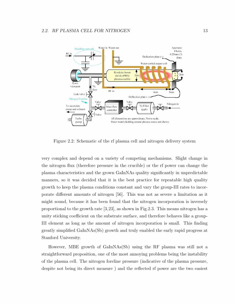
2.2 Schematic of the rf plasma cell and nitrogen delivery system . . . . . 13
2.3 Nitrogen content as a function of growth rate for GaNAs . . . . . . . 14
2.4 Trajectories of foreline pressure and reflected power before rf cell rebuild 15
2.5 Improved plasma cell stability after rebuild . . . . . . . . . . . . . . . 16
2.6 Room-temperature PL spectrum of a GaInNAsSb QW surrounded by
GaNAs barriers . . . . . . . . . . . . . . . . . . . . . . . . . . . . . . 18
2.7 PL intensity and wavelength vs annealing tempearture . . . . . . . . 19
2.8 PL spectra illustrating the benefits of antimony . . . . . . . . . . . . 21
2.9 Improvement in PL intensity by GaNAs barriers . . . . . . . . . . . . 23
2.10 PL spectra before and after purification of the nitrogen source. . . . . 24
2.11 PL improvement by using deflection plates. . . . . . . . . . . . . . . . 26
2.12 Ion current measured as a function deflection voltage. . . . . . . . . . 27
2.13 CW L-I curve and spectrum for the lowest-threshold 1.55µm laser. . . 28
2.14 Pulsed spectrum and L-I curve for a 14µm-aperture VCSEL . . . . . 28
xii

3.1 Peak PL intensity, as a function of postgrowth annealing temperature.
Inset shows the peak emission energy (as-grown) at room temperature.
From [2] . . . . . . . . . . . . . . . . . . . . . . . . . . . . . . . . . . 31
3.2 Reflectivity spectrum for an undoped wafer at various thermocouple
temperatures in 50oC steps . . . . . . . . . . . . . . . . . . . . . . . . 32
3.3 Reflectivity spectrum for an n-type wafer at various thermocouple tem-
peratures in 50oC steps . . . . . . . . . . . . . . . . . . . . . . . . . 33
3.4 Sensitivity of reflectivity measurement to wafer wobble . . . . . . . . 35
3.5 Reflectivity of different substrate structures(at 440oC). Also shown is
the pyrometer response spectrum, in arbitrary unit. . . . . . . . . . 36
3.6 1/(ehc
λkT − 1) vs. temperature, λ=886nm . . . . . . . . . . . . . . . . 37
3.7 Pyrometer measurement fluctuations for a 3-inch wafer . . . . . . . . 39
3.8 Pyrometer measurement fluctuations for a 2-inch wafer . . . . . . . . 39
3.9 Pyrometer measurement fluctuations for a quarter of 3-inch wafer . . 40
3.10 Schematic of typical wafers sizes when loaded on the substrate heater 41
3.11 Pyrometer measurement during cool-down and then heat-up, for a
quarter of 3-inch wafer . . . . . . . . . . . . . . . . . . . . . . . . . . 41
3.12 Pyrometer measurement during heat-up, for a 3-inch n-type wafer.
Small bumps are due to wafer tilting for easier RHEED observation . 43
3.13 Pyrometer measurement during heat-up, for a 3-inch undoped wafer 44
3.14 TC readings at deox in sys4 and at QW growth in sys5 . . . . . . . 44
3.15 Result of 1-minute annealing at different temperatures for GaInNAsSb
QW . . . . . . . . . . . . . . . . . . . . . . . . . . . . . . . . . . . . 47
3.16 PL intensity and wavelength vs. annealing duration for GaInNAsSb QW 48
3.17 PL intensity and wavelength vs. annealing duration for GaInNAsSb QW 49
3.18 PL intensity vs. annealing duration for Ga0.7In0.3N0.012As0.968Sb0.02 QW. 50
3.19 PL intensity vs. annealing duration for lattice-matched 150nm-thick
Ga0.92In0.08N0.02As0.98 layer. . . . . . . . . . . . . . . . . . . . . . . . 51
3.20 Ga and As equivalent pressures for which segregation-free growth hap-
pens for GayIn1−yNxAs1−x [3] . . . . . . . . . . . . . . . . . . . . . . 53
3.21 PL results for GaInNAsSb QWs, as a function of the As/III flux ratio 54
xiii

3.22 PL results versus Sb flux from [4] . . . . . . . . . . . . . . . . . . . . 54
3.23 PL intensity for different (As+Sb)/III flux ratios annealed for 1 minute 56
3.24 PL intensity at the optimum annealing temperature vs. (As+Sb)/III
flux ratio. Annealed for 1 minute . . . . . . . . . . . . . . . . . . . . 56
3.25 PL peak intensity(solid circles) and wavelength(open circles) versus
As/III ratio [5] . . . . . . . . . . . . . . . . . . . . . . . . . . . . . . 57
3.26 PL wavelength for different (As+Sb)/III flux ratios. Annealed for 1
minute . . . . . . . . . . . . . . . . . . . . . . . . . . . . . . . . . . . 59
3.27 XRD result for different (As+Sb)/III flux ratios, grown at 440oC . . . 59
3.28 SIMS result for ×4,×9, and ×15 (As+Sb)/III ratio growths, at 440oC 60
3.29 PL result for low As+Sb flux growths, after one-minute annealing . . 60
3.30 PL result for low As+Sb flux growths, after long annealing . . . . . . 61
3.31 PL sample and laser structures studied for this thesis . . . . . . . . . 62
3.32 Laser result and PL for high-indium QW . . . . . . . . . . . . . . . . 63
3.33 PL intensity and wavelength after self-annealing of plain PL samples 65
3.34 Results of additional ex-situ 1-minute annealing of 41%-In plain PL
samples after 0-, 2.5-, and 6.5-hour self-annealing . . . . . . . . . . . 66
3.35 Results of additional ex-situ 1-minute annealing on ”Laser-like” PL
samples with 41%-In QW . . . . . . . . . . . . . . . . . . . . . . . . 67
3.36 Results of long-annealing at 620oC on laser-like PL samples with 41%-
In QW . . . . . . . . . . . . . . . . . . . . . . . . . . . . . . . . . . . 68
4.1 Results of long-annealing at 620oC on laser-like PL samples with 41%-
In QW . . . . . . . . . . . . . . . . . . . . . . . . . . . . . . . . . . . 71
4.2 Schematic of the edge-emitting laser. . . . . . . . . . . . . . . . . . . 72
4.3 CW and Pulsed L-I curve for a 2050µm×20µm laser. . . . . . . . . . 73
4.4 CW spectrum of the a 2050µm×20µm laser at thermal rollover at a
chuck temperature of 15oC . . . . . . . . . . . . . . . . . . . . . . . . 73
4.5 PL intensity versus laser threshold current density [5] . . . . . . . . . 74
4.6 Band offsets of GaInNAsSb/GaNAs QWs . . . . . . . . . . . . . . . . 78
4.7 Band offsets of InGaAs/GaAs and InGaAsN/GaAs [6] . . . . . . . . . 78
xiv

4.8 Hole distribution at 300K. . . . . . . . . . . . . . . . . . . . . . . . . 80
4.9 Pulsed L-I curve for a 2050µm×20µm laser. . . . . . . . . . . . . . . 84
4.10 T0 for a 2050µm×20µm laser. . . . . . . . . . . . . . . . . . . . . . . 85
4.11 3 different QW structures . . . . . . . . . . . . . . . . . . . . . . . . 86
4.12 T0 for a thin-barrier laser, 2050µm×20µm. . . . . . . . . . . . . . . . 86
4.13 T0 for a 3QW laser, 2050µm×20µm. . . . . . . . . . . . . . . . . . . 87
4.14 T0 and Jth for all 6 sets of lasers. . . . . . . . . . . . . . . . . . . . . 88
4.15 Non-radiative current divided by the number of wells. . . . . . . . . . 89
4.16 Non-radiative current divided by total barrier width. . . . . . . . . . 89
4.17 Definition of the absorption edge and transparency point extracted
from the modal gain and loss spectra . . . . . . . . . . . . . . . . . . 90
4.18 PL intensity of GaInNAsSb QW for 20nm, 10nm, and 0 GaNAs barrier
thicknesses . . . . . . . . . . . . . . . . . . . . . . . . . . . . . . . . . 91
4.19 Two approaches to reduce leakage problem. . . . . . . . . . . . . . . 93
5.1 Round-trip gain for different number of QWs . . . . . . . . . . . . . . 97
5.2 Results of the single-pass estimate for scattering loss for laterally abrupt
aperture . . . . . . . . . . . . . . . . . . . . . . . . . . . . . . . . . . 98
5.3 Convetional PIN, intra-cavity, and tunnel-junction VCSEL strcutrures 100
5.4 Pulsed LI curve for 17µm diameter aperture. . . . . . . . . . . . . . 107
5.5 Spectrum of a pulsed 1528nm VCSEL at 1.2× threshold. . . . . . . . 108
5.6 CW LI curve of a 7 µm-aperture VCSEL . . . . . . . . . . . . . . . . 108
xv

xvi

Chapter 1
Introduction
In the early 1990’s, people were excited to exchange messages and texts through e-
mails and text-based WWW pages. Only 10 years ago, people were happy to exchange
high quality pictures and music files over the internet. Now with the advent of new
generations of internet services such as YouTube and BitTorrent, people want to share
home-made videos, download/watch HD-quality movies, or play online video games.
Despite the public notion that the internet boom of the late 1990’s ended with a
burst bubble, the actual bandwidth consumption has never stopped its exponential
increase, increasing by orders of magnitude over the last decade as shown in Fig.1.1
for Japan’s case, as consumers’ appetite for internet services ’evolved’ from text to
pictures, and to video. The Discovery Institue, a think-tank, went as far as warning
in early 2007 of a coming deluge of data that today’s networks are not remotely
prepared to handle, and named it ’exaflood’, the flood of exabytes (1018 bytes, or 1
billion gibabytes). Nemertes, a market-research firm, also warned in November 2007
that user demand for the internet could outpace capacity by 2010 [7].
The most critical part of the internet that needs upgrading is metro-area and
local area networks (MANs/LANs) that comprise the last portion of the network
connecting individual homes and offices (the so-called ”the last mile”), while the
optical backbone networks utilizing wavelength division multiplexing (WDM) can
provide data rates exceeding terabits per second over a single fiber. Currently, the
last mile links, composed of mainly ADSL (Asymmetric Digital Subscriber Line) and
1

2 CHAPTER 1. INTRODUCTION
Figure 1.1: Bandwidth usage in Japan [1]
cable internet, present a bottleneck to the end user, as their bandwidth is at most
tens of Mbps and degrades even further for longer distances or more users. This issue
can be solved by expansion of the optical network all the way to the end users, in an
approach generally called FTTx (Fiber To The Home, Premise, Node, Building, Desk,
Curb, and so on). Such an approach absolutely requires low-cost and reliable optical
components that can send high-speed data over optical fibers, while consuming as
little power as possible.
Optical fibers, which are the data transmission medium for optical networks, dic-
tate the wavelength of operation and the kind of optical components that are re-
quired. Optical fibers support the highest data rate and the longest distance at 1.3µm
and 1.55µm, because of minimum dispersion at 1.3µm and minimum attenuation at
1.55µm, as shown in Fig.1.2. While 1.55µm was the clear winner for long-haul links
across continents or oceans, 1.3µm and 1.55µm are both adequate and relatively com-
parable for MANs or LANs (i.e., a few or tens of kilometers at several tens of Gbps)
as shown in Fig.1.3. However, 1.55µm is still slightly better and also can benefit from
the availability of more advanced optical components that have been developed for
1.55µm long-haul links.
While InGaAsP/InP-based Bragg grating and distributed feedback(DFB) lasers

3
0.1
0.2
0.3
0.4
0.5
0.6
1600 1700 1400 1300 1200 1500 Wavelength (nm)
Fiber Loss
L-Band
S-Band
OH absorption peak
DWDM Metro Area Network( Uncooled CWDM )Fi
ber L
oss (
dB/k
m)
Figure 1.2: Loss spectrum of optical fibers and CWDM/DWDM wavelengths.
Figure 1.3: Repeater-less transmission distance for different sources

4 CHAPTER 1. INTRODUCTION
have been the sources for long-haul, 1.55µm optical fiber backbone networks for the
past three decades and clearly meet the distance criteria in Fig.1.3, their cost is
still far too high to meet the demands of hundreds of million lasers that need to be
deployed in MANs, LANs, and FTTx in a modern communications network architec-
ture. Vertical-cavity surface-emitting lasers (VCSELs), which amplify and emit light
in the vertical direction perpendicular to the wafer surface as shown in Fig.1.4, are
ideal for this purpose, as they possess many advantages over traditional edge-emitting
Bragg-grating or DFB lasers, such as:
• Low threshold current and low power consumption due to small mode volume
• Single longitudinal mode due to the short cavity length
• Slow change in wavelength with temperature change
• Easier and more efficient coupling into single-mode fibers, reducing alignment/packaging
costs
• Simple and robust fabrication, requiring no e-beam lithography, wafer thinning,
or facet coating
• High-density 2-D arrays for parallel interconnects
• On-wafer testing before cleaving/packaging, resulting in significant cost reduc-
tion in testing and packaging
• More devices per wafer, due to much smaller device foot-print
Despite these advantages, VCSELs at 1.3-1.6µm have been slow in coming. InP-
based GaInAsP edge-emitting lasers have been available for decades now, but com-
patible materials for making good DBR mirrors on InP have been very hard to
find. Despite this difficulty, InGaAsP QW based VCSELs have been fabricated using
metal mirrors [8], wafer bonded AlAs/GaAs mirrors [9], combined InGaAsP/InP and
AlAs/GaAs metamorphic mirrors [10], AlGaAsSb/AlAsSb mirrors [11] and dielectric

5
Figure 1.4: Schematics of an edge-emitting laser vs. a VCSEL. The mirrors for anedge-emitting laser can be cleaved/coated facets, Bragg grating, or DFB distributedover the cavity.
mirrors [12]. However, these VCSELs fall short of commercial viability, due to dif-
ficulties in growth, poor thermal/electrical conductivity, lack of manufacturability,
etc.
On the other hand, the pair of AlAs and GaAs layers grown on GaAs provides
an easy-to-grow and reliable ( due to lattice-matching ) DBR system, with high
index contrast, high electrical/thermal conductivities and good electrical/optical lat-
eral confinements by AlAs oxidation. However, realizing a gain material on GaAs
substrates that emits at 1.3-1.6µm was challenging, and approaches such as InAs
quantom dots [13] and GaAsSb/InGaAs Type II quantum wells [14] had difficulty
going over 1.3µm.
The situation changed when Weyers et al. [15] first reported reduction of bandgap
with incorporation of a small amount of nitrogen in GaAs while also reducing the
lattice constant, and later, the proposal of GaInNAs by adding nitrogen to InGaAs
[16,17] as a new optical gain material for long-wavelength lasers on GaAs substrates.
This discovery was far from obvious from the known properties of all other III-V
materials, where a smaller lattice constant usually leads to a larger bandgap, as shown
in Fig.1.5. By incorporating a proper amount of In (increasing lattice constant and
decreasing bandgap) and N (decreasing both bandgap and lattice constant), we can
reduce the bandgap much lower than had been possible before, while maintaining
relatively small lattice mismatch on GaAs, which is indicated as the vertical line
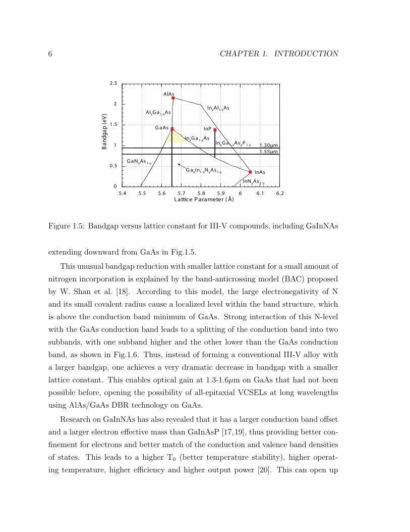
6 CHAPTER 1. INTRODUCTION
0
0.5
1
1.5
2
2.5
5.4 5.5 5.6 5.7 5.8 5.9 6 6.1 6.2
Ban
dgap
(eV
)
G aNyAs 1-y
InNyAs 1-y
InxG a1-xAs
InP
G axIn1-xNyAs 1-y
G aAs
AlAs
InAs
InxAl1-xAsAlxG a1-xAs
Lattice P arameter ( Å)
1.30µm1.55µm
InxG a1-xAs yP 1-y
Figure 1.5: Bandgap versus lattice constant for III-V compounds, including GaInNAs
extending downward from GaAs in Fig.1.5.
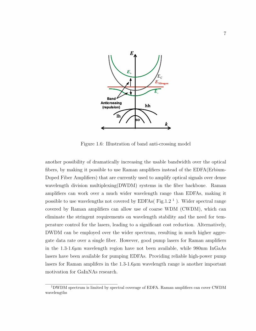
This unusual bandgap reduction with smaller lattice constant for a small amount of
nitrogen incorporation is explained by the band-anticrossing model (BAC) proposed
by W. Shan et al. [18]. According to this model, the large electronegativity of N
and its small covalent radius cause a localized level within the band structure, which
is above the conduction band minimum of GaAs. Strong interaction of this N-level
with the GaAs conduction band leads to a splitting of the conduction band into two
subbands, with one subband higher and the other lower than the GaAs conduction
band, as shown in Fig.1.6. Thus, instead of forming a conventional III-V alloy with
a larger bandgap, one achieves a very dramatic decrease in bandgap with a smaller
lattice constant. This enables optical gain at 1.3-1.6µm on GaAs that had not been
possible before, opening the possibility of all-epitaxial VCSELs at long wavelengths
using AlAs/GaAs DBR technology on GaAs.
Research on GaInNAs has also revealed that it has a larger conduction band offset
and a larger electron effective mass than GaInAsP [17,19], thus providing better con-
finement for electrons and better match of the conduction and valence band densities
of states. This leads to a higher T0 (better temperature stability), higher operat-
ing temperature, higher efficiency and higher output power [20]. This can open up
7
BandAnticrossing(repulsion)
E+
E-
ENitrogen
EC
hh
lhso
k
E
BandAnticrossing(repulsion)
E+
E-
ENitrogen
EC
hh
lhso
k
E
Figure 1.6: Illustration of band anti-crossing model
another possibility of dramatically increasing the usable bandwidth over the optical
fibers, by making it possible to use Raman amplifiers instead of the EDFA(Erbium-
Doped Fiber Amplifiers) that are currently used to amplify optical signals over dense
wavelength division multiplexing(DWDM) systems in the fiber backbone. Raman
amplifiers can work over a much wider wavelength range than EDFAs, making it
possible to use wavelengths not covered by EDFAs( Fig.1.2 1 ). Wider spectral range
covered by Raman amplifiers can allow use of coarse WDM (CWDM), which can
eliminate the stringent requirements on wavelength stability and the need for tem-
perature control for the lasers, leading to a significant cost reduction. Alternatively,
DWDM can be employed over the wider spectrum, resulting in much higher aggre-
gate data rate over a single fiber. However, good pump lasers for Raman amplifiers
in the 1.3-1.6µm wavelength region have not been available, while 980nm InGaAs
lasers have been available for pumping EDFAs. Providing reliable high-power pump
lasers for Raman amplifers in the 1.3-1.6µm wavelength range is another important
motivation for GaInNAs research.
1DWDM spectrum is limited by spectral coverage of EDFA. Raman amplifiers can cover CWDMwavelengths

8 CHAPTER 1. INTRODUCTION
While the unique properties of N incorporated in GaAs or InGaAs provide promis-
ing new possibilites for semiconductor lasers at 1.3-1.6µm, its unique properties also
posed challenges for the growth of GaInNAs. The most important challenge was the
very low solubility of nitrogen into InGaAs matrix. This is due to the different basic
crystal structures of the constituent alloys and their regions of growth compatibility:
InGaN is a hexagonal (wurtzite) crystal grown at relatively high temperatures while
InGaAs is a cubic (zincblende) crystal grown at relatively low temperatures, creating
a miscibility gap in the alloys [21–23]. When the N concentration or growth tempera-
ture increases, phase segregation occurs and the material breaks up into microscopic
regions of InGaAs and InGaN. In the case of MOVPE(Metal-Organic Vapor-Phase
Epitaxy) growths, there were additional difficulties with low cracking efficiency of
ammonia or arsine, complex precursor reactions, highly non-linear incorporation ra-
tios [24–27], or carbon and hydrogen contamination [25, 28]. MBE(Molecular Beam
Epitaxy) also had its own challenges, such as strong sensitivity to growth tempera-
ture [2] or ion damage from rf plasma cell [29], among other things. These growth
challenges become significantly more severe, as more nitrogen is added to increase the
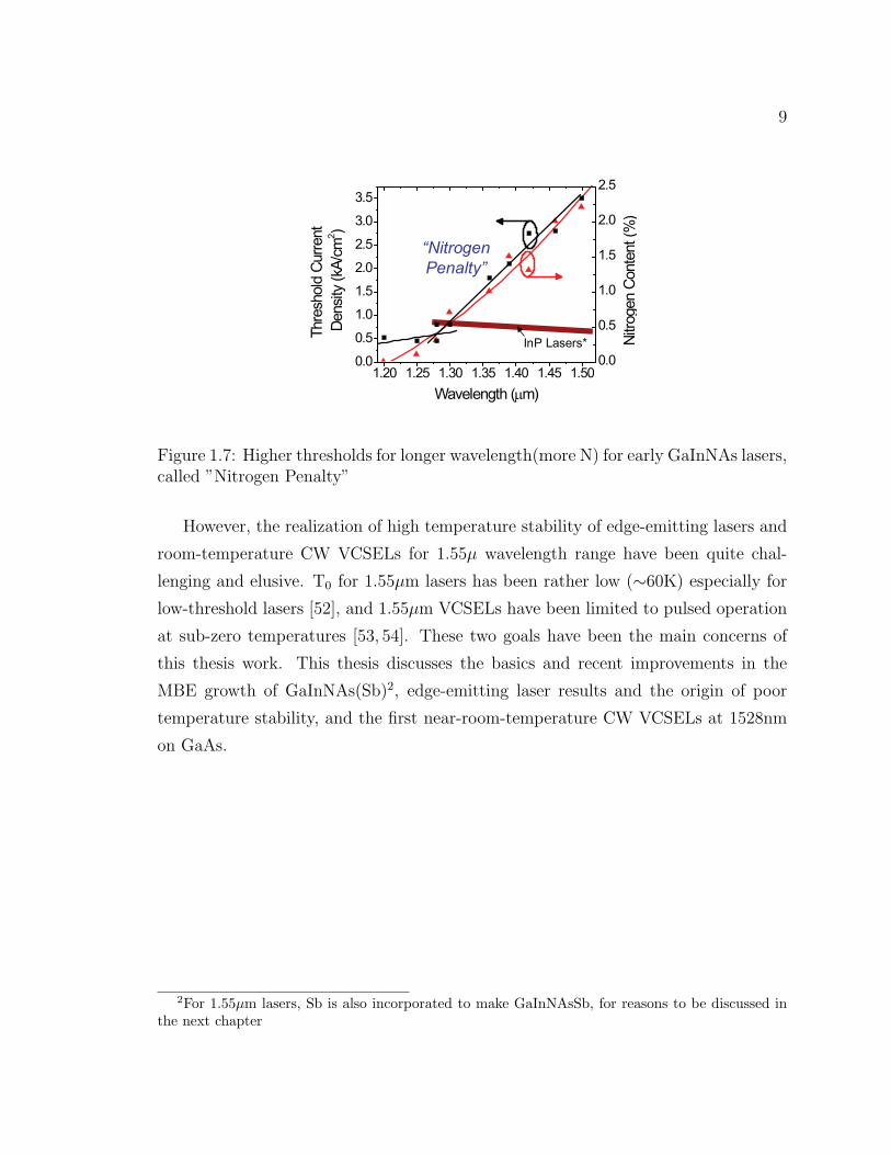
wavelength. This difficulty was initially called ’the nitrogen-penalty’, where longer
wavelength GaInNAs lasers with more nitrogen (and more indium) exhibited signifi-
cantly higher threshold current densities as shown in Fig.1.7.
Despite the challenges, immense progress has been made through intense efforts
from several research groups, and high-performance GaInNAs lasers have been real-
ized in the 1.3-1.6µm wavelength range. For the 1.3µm range, edge-emitting lasers
have been reported with room-temperature threshold current densities as low as 150-
300A/cm2 per QW for MQW lasers and 250–320A/cm2 for SQW lasers [30–35],
along with T0 values over 100K [36–39] and high output power of >8.9W [40].
Room-temperature continuous-wave(CW) VCSELs with low threshold, high output
power, high-speed direct modulation and high reliability have also been realized at
1.3µm [41–50]. 1.55µm lasers have proven to be far more challenging than 1.3µm
lasers, but we have succeeded in realizing very low threshold (318A/cm2 pulsed, and
373A/cm2 CW) and high-power(>1W pulsed, 430mW CW) lasers at 1.5µm [51] and
1.55µm [52].
9
1.20 1.25 1.30 1.35 1.40 1.45 1.500.0
0.5
1.0
1.5
2.0
2.5
3.0
3.5
0.0
0.5
1.0
1.5
2.0
2.5
Thre
shol
d Cu
rrent
Den
sity
(kA/
cm2 )
Wavelength (µm)
Nitr
ogen
Con
tent
(%)
InP Lasers*
1.20 1.25 1.30 1.35 1.40 1.45 1.500.0
0.5
1.0
1.5
2.0
2.5
3.0
3.5
Thre
shol
d Cu
rrent
Den
sity
(kA/
cm2 )
Wavelength (µm)
“NitrogenPenalty”
Figure 1.7: Higher thresholds for longer wavelength(more N) for early GaInNAs lasers,called ”Nitrogen Penalty”
However, the realization of high temperature stability of edge-emitting lasers and
room-temperature CW VCSELs for 1.55µ wavelength range have been quite chal-
lenging and elusive. T0 for 1.55µm lasers has been rather low (∼60K) especially for
low-threshold lasers [52], and 1.55µm VCSELs have been limited to pulsed operation
at sub-zero temperatures [53, 54]. These two goals have been the main concerns of
this thesis work. This thesis discusses the basics and recent improvements in the
MBE growth of GaInNAs(Sb)2, edge-emitting laser results and the origin of poor
temperature stability, and the first near-room-temperature CW VCSELs at 1528nm
on GaAs.
2For 1.55µm lasers, Sb is also incorporated to make GaInNAsSb, for reasons to be discussed inthe next chapter

Chapter 2
MBE growth of GaInNAs(Sb)
MBE(Molecular Beam Epitaxy) is used for growth of GaInNAs(Sb) QWs and lasers
reported in this thesis. This chapter provides a primer of the MBE technique and the
growth improvements that have led to the first VCSELs and the best edge-emitting
lasers near 1.5µm. This chapter is meant to be a short review and to compliment the
many excellent works of previous students [3, 55–59], so only essentially necessary or
new information is presented here. ”GaInNAs(Sb)” is used to include both GaInNAs
and GaInNAsSb materials, and the reason of including Sb is explained in this chapter.
2.1 Molecular Beam Epitaxy for GaInNAsSb growth
Molecular beam epitaxy system is essentially a highly sophisticated thermal evap-
oration system. A schematic of an MBE chamber is shown in Fig.2.1. The MBE
growth of semiconductor films takes place by the reaction of molecular beams of
the constituent elements with a crystalline substrate surface held at a suitable sub-
strate temperature under UHV conditions. The molecular beams are generated from
sources contained in ceramic crucibles (typically pyrolytic boron nitride, or PBN),
called effusion cells. The molecular beam flux intensity is accurately adjusted by the
temperature within the effusion cell. To initiate or terminate the molecular beam flux
of an individual effusion cell, each source is equipped with an externally controlled
mechanical shutter. By opening/closing the shutters in proper sequences, complex
10

2.1. MOLECULAR BEAM EPITAXY FOR GAINNASSB GROWTH 11
Effusion Cells
Effusion Cells
ShuttersShutters
RHEED Gun
RHEED Gun
Substrate Holder & Heater
Substrate Holder & Heater
Fluorescent Screen
Fluorescent Screen
View PortsView Ports
Cryoshroud
Gate Valve to Buffer
Chamber
Gate Valve to Buffer
Chamber
Ion GaugeIon Gauge
SampleSample
Figure 2.1: Schematic of an MBE chamber
multilayer heterostructures can be grown with high precision.
Because MBE growth is conducted under ultra high vacuum (UHV, ∼ 10−10
torr), the level of residual gas in the chamber and contaminant incorporation is very
low. The low pressures also lead to long mean free paths for the source atoms. As a
result, there are no precursor interactions. The substrate surface is thermally isolated
from the rest of the chamber and the effusion cells, so the physical and chemical
reactions on the substrate surface are solely determined by the substrate temperature,
independent of the growth rates. Stoichiometric compound semiconductors are quite
straightforward to grow by MBE, because at typical MBE growth temperatures, the
group-III sticking coefficient is much higher on a group-V terminated surface than
on a group-III terminated surface. Likewise, group-V elements stick to a group-III
terminated surface much more strongly than to a group-V terminated surface [60].
MBE growth of III-V compound semiconductors is usually done under a high group-V
flux with the lower group-III flux controlling the growth rate. These properties of
MBE dramatically simplify growth compared to the competing MOVPE technique,
where high-precision growth control and high quality growth require much more work
due to high carbon/hydrogen levels and complex interactions between precursors in

12 CHAPTER 2. MBE GROWTH OF GAINNAS(SB)
the gas phase and on the substrate surface. Therefore, it is the preeminent growth
technique for pioneering new materials and devices, which also has been true for
GaInNAs. The first GaInNAs study and the first GaInNAs VCSEL near 1.3µm were
realized using MBE [17], although with gas sources which caused some complications
from H incorporation [61, 62]. The best edge-emitting lasers and the first VCSEL
were all realized using MBE growth [52,53].
2.2 RF plasma cell for nitrogen
Nitrogen needs special attention for MBE growth of GaInNAs(Sb), because the most
abundant source of nitrogen on earth - nitrogen gas - is a very non-reactive substance,
which is often treated as ’inert’ for many practical purposes, including many semicon-
ductor fabrication processes. A more reactive source of nitrogen has to be provided
for GaInNAs(Sb) growth. Nitrogen-containing gases such as U-dimethylhydrazine (U-
DMHy) or ammonia, which are often used for MOVPE growth, can be considered,
but complications due to carbon/hydrogen incorporation or low cracking efficiency
make this approach rather undesirable [62,63]. On the other hand, a nitrogen plasma
is employed to provide a reactive nitogen species for GaInNAs(Sb) growth.
For our group and many other research groups, RF plasma cells have proven to be
the simplest and most effective system to grow GaInNAs(Sb) using MBE [5,52,64–67].
By contrast to RF plasmas, electron cyclotron resonance(ECR) [68] and dc plasmas
[69] were found to generate more ions and generally produce dilute-nitride material
of poorer quality [56].
We used a RF plasma cell from SVT associates. The setup of the plasma cell is
shown in Fig.2.2. The plasma was operated in an inductively-coupled mode (high-
intensity mode) to more effectively generate reactive species. The plasma conditions
are mainly determined by the pressure in the crucible and the rf power. Generally,
higher pressures or lower powers tend to decrease the ion count and the ion energy,
but also the dissociation efficiency. Lower pressures or higher powers, on the con-
trary, can increase the dissociation efficiency at the cost of more damaging ions. The
optimum points can be found by experiments [70], but the plasma conditions are
2.2. RF PLASMA CELL FOR NITROGEN 13
Figure 2.2: Schematic of the rf plasma cell and nitrogen delivery system
very complex and depend on a variety of competing mechanisms. Slight change in
the nitrogen flux (therefore pressure in the crucible) or the rf power can change the
plasma characteristics and the grown GaInNAs quality significantly in unpredictable
manners, so it was decided that it is the best practice for repeatable high quality
growth to keep the plasma conditions constant and vary the group-III rates to incor-
porate different amounts of nitrogen [56]. This was not as severe a limitation as it
might sound, because it has been found that the nitrogen incorporation is inversely
proportional to the growth rate [3,23], as shown in Fig.2.3. This means nitrogen has a
unity sticking coefficient on the substrate surface, and therefore behaves like a group-
III element as long as the amount of nitrogen incorporation is small. This finding
greatly simplified GaInNAs(Sb) growth and truly enabled the early rapid progress at
Stanford University.
However, MBE growth of GaInNAs(Sb) using the RF plasma was still not a
straightforward proposition, one of the most annoying problems being the instability
of the plasma cell. The nitrogen foreline pressure (indicative of the plasma pressure,
despite not being its direct measure ) and the reflected rf power are the two easiest

14 CHAPTER 2. MBE GROWTH OF GAINNAS(SB)
Figure 2.3: Nitrogen content as a function of growth rate for GaNAs
parameters to monitor for the plasma conditions, and they showed a very rapid change
during the first hour of plasma operation, as shown in Fig.2.4. Moreover, the plasma
would sometimes refuse to ignite at all or become extinguished in the middle of
a growth for no apparent reason. This instability in the plasma conditions added
some grievance and one more parameter to optimize in our efforts to find the best
way to control the plasma cell. Various measurements, such as optical spectrum
of the plasma and ion energy/count measurements, were conducted [56], and many
samples were grown and compared to determine when the plasma was in its best
condition, but the results were inconclusive. The origin of the instability was also
not clear, although thermal effects on the crucible or the capacitor in the matching
network were suspected [56]. An in-depth analysis was presented in [56] based on the
hypothesis that a large drift in the capacitor temperature is the main cause of this
instability problem, but later measurements showed that the capactitor temperature
is very stable within 2-3oC, thus disproving the capacitor temperature hypothesis.
Part of this instability problem was resolved when the rf cell was repaired after
producing low-quality materials for many months. With the repair, a significant
change was made to the configuration of the crucible. Before the repair, the crucible
was an open-ended cylinder with a separate aperture plate (thin and coin-shaped)

2.3. PHOTOLUMINESCENCE 15
(a) Foreline Pressure (b) Re�ected RF power
Figure 2.4: Trajectories of foreline pressure and reflected power before rf cell rebuild.The cell was rebuilt in mid-2006, so both lines are before the rebuild.
held in place between the crucible and the deflection plates. After the repair, a new
crucible with the aperture plate now integrated as part of the crucible was installed.
This resulted in a significant improvement in the cell stability, reaching steady-state
within 20 minutes rather than drifting for over 1 hour, as shown in Fig.2.5. The
new crucible also required much less nitrogen flow rate ( only 0.115 sccm, compared
to 0.5 sccm ) for comparable plasma conditions and foreline pressures. Therefore, it
seems that much of the instability was due to the mechanical drift of the separate
aperture plate under temperature and pressure variations. We also found that as
long as we kept the same foreline pressure as before, the nitrogen incorporation in
and the optical quality of GaInNAs(Sb) were essentially the same, comparing samples
before and after the installation of the new crucible. This was a welcome news for
us in that it proved that the foreline pressure is actually a very good indicator of the
plasma conditions, and the research can be continued without restarting everything
from scratch, with a more stable plasma cell, despite a major equipment modification
in the course of the research.
2.3 Photoluminescence
PL has been the most important characterization technique for the research of high-
quality of GaInNAs(Sb) growth, so it deserves special mention in this chapter. Other

16 CHAPTER 2. MBE GROWTH OF GAINNAS(SB)
(a) Foreline Pressure (b) Re�ected RF power
BeforeBefore
After
After
Figure 2.5: Improved plasma cell stability after rebuild
measurements such as XRD(X-Ray Diffraction), TEM(Transmission Electron Mi-
croscopy), and SIMS(Secondary Ion Mass Spectroscopy) were also used. SIMS mainly
measures the compositions of the main constituent elements and some impurities in
the grown films, XRD measures the crystalline quality, the strains and the composi-
tion, and TEM can take a real-space image of the actual atoms in the crystal, enabling
us to directly see the defects, compositional fluctuations, interface quality, etc. These
methods were all important, but PL was by far the most often used technique (i.e.,
for each and every sample after growth, rather than a few select samples for other
techniques) and also the most sensitive to opto-electronic properties. Simply put,
good quality indicated by XRD, TEM, or SIMS does not guarantee a good PL result,
while a good PL result most probably means high crystalline quality and low level
of impurities. More importantly, the PL result and laser performance have shown
very strong positive correlation [5, 52], and many growth improvements discussed
in this chapter were first identified by PL measurement and later corroborated by
actual laser results. Therefore, only the PL technique is presented in this section,
and the reader is referred to previous theses from our group for the details of other
techniques [3, 56–58].
The PL technique consists of an incident pump beam with photon energy larger
than the bandgap of the material being studied. The pump generates electron-hole
pairs in the semiconductor. They quickly(∼0.1ps) thermalize to the lowest energy of
their respective bands. The carriers then diffuse and eventually recombine, emitting

2.3. PHOTOLUMINESCENCE 17
a photon close to the bandgap energy. However, the carriers may recombine in other
ways than emitting a photon, most notably, through Schockley-Read-Hall(SRH), or
defect recombination. Higher quality of the material would therefore lead to more
recombination occurring radiatively, while lower quality material would lose a sig-
nificant number of carriers through defect recombination. So the intensity of the
radiative emission correlates positively with the material quality, and serves as an
indicator of quality.
The PL setup employed in this work uses a chopper to modulate the pump laser
(which was initially an Argon laser and later replaced with a 532nm frequency-doubled
semiconductor laser). The emission signal passes through a monochramator to select
a specific wavelength, and is then detected by a photo-detector. The detector signal is
fed to a lock-in amplifier for maximizing the signal-to-noise ratio. As the wavelength
response of this setup is not flat due to the spectral responses of the detector and
the monochromator grating, each PL measurement is normalized by dividing by the
system response, which was measured from the system response to a white light
source. The PL measurement results also showed run-to-run variations due to day-
to-day variations in the pump laser power, alignment, and so on, so a standard sample
was measured for every run and the results were normalized with respect to the peak
PL intensity of the standard sample.
The main parameters of interest for PL measurements are the wavelength of peak
intensity, peak intensity, and linewidth. The wavelength of peak intensity is obvisouly
of great interest, as it is quite close to the bandgap and where lasing would occur with
such an active layer. Peak intensity is an excellent indicator of the optical quality of
the material. The lower the defect density, the stronger the peak PL signal. Caution
has to be exercised in comparing the peak PL intensities of different samples, however,
because the peak PL intensity provides only a relative measure of the material quality,
in that the peak intensity can be different even for the same quality material if its
surrounding layers are of a different structure or quality. However, peak PL intensity
has served as an excellent predictor of laser performance over several generations
of lasers at Stanford as well as other research groups [5], as long as the same test
structure is used over all the samples being compared. The linewidth is an indicator
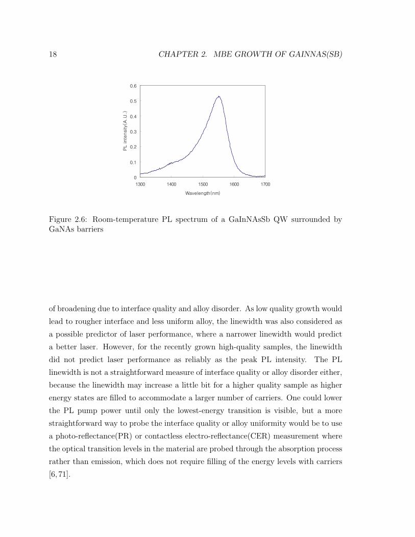
18 CHAPTER 2. MBE GROWTH OF GAINNAS(SB)
0
0.1
0.2
0.3
0.4
0.5
0.6
1300 1400 1500 1600 1700
Wavelength(nm)
PL inte
nsi
ty(A
.U.)
Figure 2.6: Room-temperature PL spectrum of a GaInNAsSb QW surrounded byGaNAs barriers
of broadening due to interface quality and alloy disorder. As low quality growth would
lead to rougher interface and less uniform alloy, the linewidth was also considered as
a possible predictor of laser performance, where a narrower linewidth would predict
a better laser. However, for the recently grown high-quality samples, the linewidth
did not predict laser performance as reliably as the peak PL intensity. The PL
linewidth is not a straightforward measure of interface quality or alloy disorder either,
because the linewidth may increase a little bit for a higher quality sample as higher
energy states are filled to accommodate a larger number of carriers. One could lower
the PL pump power until only the lowest-energy transition is visible, but a more
straightforward way to probe the interface quality or alloy uniformity would be to use
a photo-reflectance(PR) or contactless electro-reflectance(CER) measurement where
the optical transition levels in the material are probed through the absorption process
rather than emission, which does not require filling of the energy levels with carriers
[6, 71].

2.4. ANNEALING 19
0
0.1
0.2
0.3
0.4
0.5
550 600 650 700 750 800 850
Temperature(C)
PL in
tens
ity(A
.U.)
1480
1500
1520
1540
1560
1580
1600
1620
550 600 650 700 750 800 850
Temperature(C)
Wav
elen
gth(
nm)
(a) Peak PL intensity (b) Peak PL Wavelength
Figure 2.7: PL intensity and wavelength vs annealing tempearture. 580oC represents’no anneal’.
2.4 Annealing
Annealing has been an integral part of GaInNAs(Sb) research from the early days [27,
28, 72]. Annealing of GaInNAs(Sb) has two major effects on its properties: increase
in the optical quality (measured by PL) and blueshift in the peak PL wavelength.
Many defects are formed during growth of GaInNAs(Sb), which is believed to
result from the low growth temperature required to incorporate N and In, and the
damage due to energetic species in the nitrogen plasma. A 60 second anneal in an
RTA(Rapid Thermal Anneal) chamber has been typically employed by our research
group, obtaining a significant PL intensity increase compared to the un-annealed sam-
ple as shown in Fig.2.7. Researchers have identified many types of defects and their
behavior when annealed. Among the most prominent are nitrogen split interstitials
(two nitrogen on one group-V site, or (N-N)As), and arsenic-nitrogen split interstitials
(As-N)As, giving rise to various electron and hole trap levels in the material [73–75].
Another important defect is arsenic anti-sites (an arsenic atom on a group-III site, or
AsGa), due to the low growth temperature and high arsenic flux. Presence of this type
of defects can be supported by the significant improvement in luminescence efficiency
and laser performance when lower arsenic flux was used for growth, as reported by the
Infineon group [5] and by our group [76] and described in Section 3.3 of this thesis.
20 CHAPTER 2. MBE GROWTH OF GAINNAS(SB)
It is worth noting that PL intensity improves with anneal up to a certain tem-
perature, above which the intensity starts to fall again. Various mechanisms have
been proposed as a cause(s) of this behavior, such as arsenic vacancies diffusing from
the surfrace or elsewhere in the substrate, outdiffusion from the QW [77], strain re-
laxation, or phase segregation [56]. It is found for our GaInNAs(Sb) QWs that this
quality drop under over-annealing has a rather large activation energy (∼7eV) which
may indicate an extended type of defect, such as dislocations. A very similar anneal-
ing behavior was observed for two samples with vastly different cladding structures
but with the same QWs, which can be evidence against the importance of arsenic
vacancies in the over-annealing mechanism. More will be discussed in Chapter 3.
The other major effect of annealing GaInNAs(Sb) is the blueshift of the peak PL
wavelength, as shown in Fig.2.7. The origin of the blueshift was attributed to various
mechanisms, such as nitrogen outdiffusion [3, 23, 78], In/Ga interdiffusion [79–81],
and locazlied depressions in bandgap [82–84] due to nitrogen clusters or point defects
that are removed with anneal. Later research indicates that changes in the nearest-
neighbor configuration of nitrogen during annealing can explain the majority of this
blueshift, when gallium and indium atoms trade places so each nitrogen is surrounded
by more indium atoms, in order to reduce the local strain and the total energy of the
lattice [85, 86]. One source of discrepancies between groups as to the origin of the
blueshift was the presence or absence of vacancies in the crystal. It has been shown
that intentional introduction of vacancies in the crystal causes more interdiffusion of
atoms and thus more blueshift [87–89]. Thus, it is expected that the best quality
material should demonstrate the least blueshift with anneal. The GaInNAs(Sb) QWs
grown by our group and used in the low threshold 1.5µm and 1.55µm lasers indeed
show very negligible blueshift, apart from the initial large blueshift due to the nitrogen
nearest-neighbor reconfiguration (See Fig.3.16).
2.5 Overcoming the Nitrogen Penalty
As described in the previous chapter, there was initially a significant degradation
in the material quality and increase in the laser threshold, as researchers tried to

2.5. OVERCOMING THE NITROGEN PENALTY 21
0.75 0.80 0.85 0.90 0.95 1.00
100
101
102
103
1600 1500 1400 1300
More In, Sb, N
GaInNAsSb
GaInNAs
GaInNAs
PL In
tens
ity (a
.u.)
Energy(eV)
Wavelength (nm)
More In and N
Figure 2.8: PL spectra illustrating the benefits of antimony
increase the wavelength by increasing nitrogen and indium content in GaInNAs. This
section briefly describes important breakthroughs that enabled low-threshold room-
temperature continous-wave edge-emitting lasers at 1.55µm [52] and the first all-
epitaxial GaAs-based VCSELs at 1.46µm and 1.534µm [53,54].
2.5.1 Addition of Antimony
The quality of GaInNAs showed rapid degradation going beyond 1.3µm with more
In and N added to increase the wavelength [27,28,45,78]. Addition of antimony was
found to solve this problem, enabling high quality growth for higher In and N contents,
as illustrated in Fig.2.8. Antimony acts as a reactive surfactant, which reduces the
surface diffusion length by occupying substitutional sites [90]. This reduction of the
surface mobility suppresses phase segregation and roughening, allowing growth at
higher temperatures. Higher growth temperature enables growth of higher quality
material with fewer point defects.
In addition to acting as a reactive surfactant, Sb was also found to incorporate into
the alloy ( on the order of a few percents ), which helped further reduce the bandgap.
GaInNAsSb QWs, which are obtained by adding Sb to GaInNAs, have been essential
for realizing high performance edge-emitting lasers and the first VCSELs at 1.55µm

22 CHAPTER 2. MBE GROWTH OF GAINNAS(SB)
by our group [52, 54]. It is also possible to reach 1.5µm without using Sb, but the
laser thresholds were significantly higher than achievable with GaInNAsSb [5].
Another interesting effect of antimony is that it increases the nitrogen incorpo-
ration rate by about 50%, due to its properties as a reactive surfactant [91, 92] and
its large atomic size, making more room for N to incorporate without increasing the
lattice free energy too much. Probably due its large size, antimony tends to com-
pete against indium for incorporation, despite one being a group-V element and the
other a group-III element [93]. Lastly, there exists an optimal flux of antimony for
the best quality growth: the Sb flux has to be sufficiently high to provide surfactant
effects, but not too high to reduce the surface difussion length too much, degrading
the optical quality of the material [93].
2.5.2 GaNAs barrier
Use of GaNAs barrier layers was another important step toward achieving high-quality
GaInNAs(Sb) QWs. For 1.3-1.55µm emission, GaInNAs(Sb) has a rather high con-
centration of indium(30-40%), which results in quite high compressive strain in the
QW (∼2.5% for 1.55µm QWs) even with the lattice constant reduction from N in-
corporation. Use of GaNAs barriers was proposed as a way to compensate this high
compressive strain, by providing an opposing tensile strain below and above the GaIn-
NAs(Sb) layer [3, 23, 79, 94]. The effect of GaNAs barriers on the peak PL intensity
is shown in Fig.2.9. GaNAs barriers lead to roughly 4 times higher PL intensity
compared to GaAs barriers. In addition to improving the quality of a GaInNAs(Sb)
single QW, strain compensation provided by GaNAs barriers also helps with growing
multiple QWs. Up to 3 QWs have been grown with high quality, which were actually
used for the VCSEL results of our group [53, 54, 95], while SQWs were used for high
performance edge-emitting lasers [52,96].
GaNAs was also helpful in extending the emission wavelength, because it has a
smaller bandgap than GaAs. Lower barrier energy leads to lower QW confinement
energies, resulting in longer emission wavelength. It was also initially proposed that
GaNAs can act as a reservoir of nitrogen, which can reduce the blueshift due to

2.5. OVERCOMING THE NITROGEN PENALTY 23
550 700 750 8000.00
0.05
0.10
0.15
0.20
0.25
0.30
0.35
0.40
0.45
PL In
tens
ity (a
.u.)
Anneal Temperature (oC)
GaNAs barrier
GaAs barrier
Figure 2.9: Improvement in PL intensity by GaNAs barriers
the nitrogen outdiffusion from GaInNAs(Sb) [23], but this effect seems to be less
important for later high-quality GaInNAs(Sb) growths.
Although GaNAs has been one of the enabling factors for 1.55µm GaInNAs(Sb)
lasers, now it is turning out to be a performance bottleneck. While GaNAs barriers
improve the quality of GaInNAs(Sb), the quality of GaNAs itself remains relatively
poor with a high concentration of point defects [73, 92, 97]. The small bandgap of
GaNAs also means smaller band offset between GaInNAs(Sb) and GaNAs layers,
resulting in more carriers in the GaNAs barriers when compared to GaAs barriers.
The unfortunate combination of low quality and low band offset leads to significant
carrier loss in the GaNAs layers, unnecessarily increasing the laser threshold and also
degrading the temperature stability of the lasers. A new barrier design is necessary
that can solve this problem while retaining the advantages of strain compensation.
More details about this issue are presented in Chapter 4.
2.5.3 Impurities in the Nitrogen Beam and the MBE cham-
ber
The background pressure (10−10 torr) and the fluxes of source elements (on the order
of 10−7 torr measured by an ion gauge) are very low in MBE, so even a barely

24 CHAPTER 2. MBE GROWTH OF GAINNAS(SB)
Figure 2.10: PL spectra before and after purification of the nitrogen source.
detectable quantity of comtaminants can result in significant levels of impurities in the
grown material. Therefore, minimizing background comtaminants (such as H2O, O2,
CO2, and other hydrocarbons) in the MBE chamber is of paramount importance for
growing high quality materials. As GaInNAs(Sb) growth requires a nitrogen plasma
source, the nitrogen source gas has to be very clean too. Although 5N(99.999%) high-
purity nitrogen gas is used as the source, 0.001% impurity in the nitrogen beam can
lead to a high level of impurities in the crystal when nitrogen is incorporated at the
concentration of several 1020cm−3. Deliberate care was taken to remove impurities
from the nitrogen beam, by installing a part-per-billion purifier, carefully baking the
nitrogen delivery lines, and fixing a leak in the pumping system. This resulted in a
significant improvement in the PL intensity, as shown in Fig.2.10. Impurity levels
were checked using a residual gas analyzer installed on the growth chamber, to make
sure oxygen and water levels are below the detection limits, every time a major
maintenance or modification work was performed on the chamber, especially when
the rf plasma cell was rebuilt.
Maintaining low background pressure in the MBE growth chamber is also very
important, without which one cannot embark on any meaningful growth experiments.
Although this is a conceptually simple task, in practice it is arguably the most im-
portant and the most time-consuming aspect of MBE growth research, requiring days

2.5. OVERCOMING THE NITROGEN PENALTY 25
and weeks of repairs, bakes, and leak checking, although it does not merit much dis-
cussion in a thesis. However, one particular problem that plagued our MBE chamber1
for a decade or so is worth describing. The chamber pressure would rise to 10−7 or
10−6 torr at a random moment for no apparent reason. The high pressure would
stay for a few minutes, and then drop abruptly down to the 10−10 torr range. This
problem was dubbed quite appopriately as ”System5 burps”. The origin of and the
solution of this burping problem was not found over many generations of students,
although some hypotheses were proposed, such as permeation of cooling water and
ethylene glycol through the stainless steel wall of the source cooling panel. This prob-
lem was eventually found to be due to a clogging at the liquid nitrogen valve, which
sits between the liquid nitrogen reservoir in the ceiling of the laboratory room and
the cryoshroud in the MBE chamber2. Due to the clogging, the cryoshroud would
be insufficiently filled, leading to less effective pumping action and slow rise in the
chamber pressure, and then a rapid decrease when liquid nitrogen suddens flows into
the cryoshroud with a refill of the reservoir. This problem was permanently resolved
by emptying the liquid nitrogen system completely and drying the whole system with
dry air, which probably removed small particles of dust or ice that were deposited at
the valve.
The most troublesome implication of the burp problem is that some of previous
experiments might have been affected by one of these burps. Since System5 burps
would manifest themselves at random moments without any warning, there was al-
ways some uncertainty whether low optical quality of a particular sample was a real
meaningful result or just a victim of a burp3. Although we believe previous exper-
iments were properly analyzed taking any possible ’burp victims’ into account, one
needs to stay open-minded and prepared for any surprise findings that contradict
1This problem was persistent in System5, which is dedicated for GaInNAsSb growth, while theother System4 is dedicated for AlGaAs cladding and DBR growths. Two chambers are neededbecause of limited number of source materials per chamber, and also the advantage of separating Aland N cells
2The cryoshroud filled with liquid nitrogen acts as a large and effective vacuum pump by adsorbinggas molecules onto its outer surface.
3We do not monitor the chamber pressure during growth, to minimize contaminant outgassingfrom the ion gauge and also to maximize the life span of the ion gauge, which is inversely proportionalto the chamber pressure.

26 CHAPTER 2. MBE GROWTH OF GAINNAS(SB)
550 700 750 8000.0
0.2
0.4
0.6
0.8
Peak
PL
Inte
nsity
(A.U
.)
Anneal Temperature (oC), 1 minute
As-grown
WithDeflection Plates
Figure 2.11: PL improvement by using deflection plates.
previous experiments performed when the burps were still present.
2.5.4 Avoiding ion damage
Although a rf plasma cell was found to produce fewer ions than other types of plasma
cells, there are still a significant number of ions generated in a rf plasma cell. The
energy distribution of ion and electron currents from the plasma were measured by
Wistey using the chamber ion gauge as a remote Langmuir probe [56, 98]. It was
found that electrons have energies up to 8eV, and the electron current was about
4nA. Ions were found to have energies up to 35eV, with the toal ion current of ∼1nA.
To see the effect of ion removal from the plasma output, metal plates were installed
at the exit aperture of the nitrogen plasma cell. One plate was grounded and the other
was biased. From the calculation based on the measured ion energies and also by PL
measurements on samples grown with different deflection voltages, it was found that
20V is sufficient to deflect the ions away from the wafer, and the PL intensity was
uniformly high for +100, +15, and -40V, whereas 0V resulted in poorer PL intensity
as shown in Fig.2.11. Ion count measurements for different deflection voltages agree
with this result, too, as shown in Fig.2.12. On the other hand, the PL wavelength did
not change much with the application of deflection plates, which implies that nitrogen

2.5. OVERCOMING THE NITROGEN PENALTY 27
Figure 2.12: Ion current measured as a function deflection voltage.
incorporation in GaInNAsSb happens mainly by excited atoms or molecules, rather
than ions. Another interesting thing to note is that the initial experiments with
deflection plates used a much higher voltage (+800V and -800V), but this resulted in
arcing to the ground in the cell, resulting in no PL improvement [59].
Another technique used to protect the wafer surface from the plasma was arsenic
capping. A thick layer of arsenic was deposited after growth of a bottom cladding or
a bottom DBR, by keeping an arsenic flux of ∼10−6 torr for 30 minutes to 1 hour
while cooling the wafer down to 40oC. The arsenic cap can be easily desorbed by
heating the wafer above ∼400oC. This arsenic cap is used to protect the wafer surface
during plasma ignition by igniting the plasma before desorbing the capping. Because
the plasma operates in a more ion-rich condition ( low flow and high rf power ), it
is worthwhile to protect the wafer during plasma ignition. Significantly higher PL
intensity was observed for an arsenic-capped sample than a non-capped sample, and
the good laser results were obtained using arsenic capping technique [52,54,56,99].
2.5.5 Laser results
Using the growth improvements described in this chapter, the lowest reported thresh-
old 1.55µm GaInNAsSb edge-emitting lasers and the first VCSELs at 1534nm were

28 CHAPTER 2. MBE GROWTH OF GAINNAS(SB)
Figure 2.13: CW L-I curve and spectrum for the lowest-threshold 1.55µm laser.
8
10-5
10-6
10-7
10-8
10-9
ytisnetni gol,
a.u
.
l , nm1530 1532 1534 1536 1538
0.030
0.025
0.020
0.015
0.010
0.005
0
peak
po
Wm ,re
w
current, mA0 20 40 60 80 100 120
(a) Output spectrum (b) L-I curve
Figure 2.14: Pulsed spectrum and L-I curve for a 14µm-aperture VCSEL
realized.
Fig.2.13 shows the CW L-I curve and the spectrum for the 1.55µm lasers re-
ported in [52]. The threshold current density of 318A/cm2 for pulsed operation and
373A/cm2 for CW operation is the lowest threshold ever reported for GaAs-based
1.55µm lasers. CW output power reached 250mW (both facets) and pulsed output
power reached 650mW (limited by the laser driver, not by the laser itself). This comes
very close to realizing the potential of GaInNAs(Sb) material for 1.3-1.6µm lasers.
However, the temperature stability was not as good as was expected, as shown by its
relatively low T0 value (71K up to 35oC and only 21K above 35oC).

2.5. OVERCOMING THE NITROGEN PENALTY 29
Fig.2.14 shows the pulsed VCSEL results emitting at 1534nm. This was the
first-ever VCSEL at this wavelength range grown on GaAs, which is a significant
achievement, but the VCSEL required significant cooling (below -25oC) and it still
operated only in pulsed-mode.
In the following chapters, additional growth and annealing improvements and
the results of edge-emitting lasers and the first near-room-temperature CW VCSEL
results at 1528nm employing the improvements and careful design efforts.

Chapter 3
Advances in GaInNAsSb growth
3.1 Substrate temperature
Substrate temperature has always been an important growth parameter for molecular
beam epitaxy (MBE) [100, 101], along with the fluxes from the effusion cells. GaIn-
NAs(Sb) has been no exception [2, 5, 102]. We observed a distinct optimum growth
temperature at 440◦C, while the quality degraded by about a factor of two when the
temperature is off by 20◦C (Fig. 3.1). Therefore, accurate control of the substrate
temperature is very important to achieve high quality GaInNAsSb growth reliably
and repeatedly.
The MBE chamber has a thermocouple on the substrate heater assembly for mea-
suring the substrate temperature. But this thermocouple provides a very unreliable
measurement of the substrate temperature. The intrinsic accuracy of the thermo-
couple is not the problem, as its accuracy is often within 2 or 3 degrees [103] for
temperatures below 600◦C. The real problem is that the thermocouple(TC) is not in
direct contact with the wafer, far removed from it with a sapphire diffuser plate sitting
in between. As a result, the temperature measured by the thermocouple can be 100
or 200 degrees Celcius off from the actual wafer temperature, and worse, the offset is
dependent on the size, doping, material, surface quality and mounting method of the
wafer.
However, the reproducibility of desorption temperature of the GaAs surface oxide
30

3.1. SUBSTRATE TEMPERATURE 31
Figure 3.1: Peak PL intensity, as a function of postgrowth annealing temperature.Inset shows the peak emission energy (as-grown) at room temperature. From [2]
[104] has provided a very reliable temperature reference at 582◦C. This temperature
is also an appropriate temperature for growing high-quality GaAs or AlGaAs layers,
so the inaccuracy of TC measurement presented no serious problems for these layers.
But the growth temperature for GaInNAsSb is lower than that by 140◦C, for which
another reliable method for temperature measurement is required.
We initially tried bandgap thermometry, which uses the temperature-dependent
bandgap shift of semiconductors. This technique enabled us to do a growth tem-
perature study as in [2], but this was not applicable to doped wafers or complex
hetero-structures. Pyrometry measures temperature by measuring the blackbody ra-
diation from the wafer. Pyrometry also has some practical limitations, but it proved
sufficiently accurate and reliable for growth of GaInNAsSb QWs. More details are
discussed in the following subsections.
3.1.1 Bandgap Thermometry
The bandgap of a semiconductor decreases with temperature, so by measuring the
bandgap, one can determine the temperature of the wafer with great accuracy and
precision, as decribed by Hellman [105]. The best measurement would be provided

32 CHAPTER 3. ADVANCES IN GAINNASSB GROWTH
950 1000 1050 1100 1150 1200 1250 13000.44
0.46
0.48
0.5
0.52
0.54
0.56
0.58
0.6
λ (nm)
R (
appr
ox u
nits
)D:\HPBAE\Refl_pyro\2005_04_prep\s719TC=400oC
TC=750oC
500oC
600oC
Figure 3.2: Reflectivity spectrum for an undoped wafer at various thermocoupletemperatures in 50oC steps
by placing a light source behind the wafer and measuring transmission(absorption)
through the wafer. While it would be very convenient to use the substrate heater as
the light source, as in [105], the heater radiation was too weak at the QW growth
temperatures, and it is not practical to install another light source or fiber on the
heater assembly in the MBE chamber.
We used a reflectivity measurement instead, by irradiating the wafer with a 20W
halogen lamp installed at one ellipsometry port and detecting the reflection spectrum
from the other ellipsometry port. We were able to observe band edge transitions
shifting with temperature as shown in Fig. 3.2. Fitting the measured band edge
transitions with Varshni parameters, we were able to determine the growth temper-
ature for the QW. This technique was essential in our growth temperature study [2].
Unfortunately, the reflective bandgap thermometry method has a few serious prac-
tical difficulties. Many of the problems are due to the reflective setup, whereby the
most useful signal comes from those optical rays that enter the wafer through the
front surface, go through the wafer, reflect at the backside, travel back to the front
surface, and then leave the front surface to reach the detector. This is a significantly
smaller signal than the direct specular reflection off of the wafer that does not go

3.1. SUBSTRATE TEMPERATURE 33
950 1000 1050 1100 1150 1200 1250 13000.4
0.42
0.44
0.46
0.48
0.5
0.52
0.54
λ(nm)
R (
appr
ox u
nits
) D:\HPBAE\Refl_pyro\2005_04_prep\n722
TC=400oC
TC=750oC
500oC600oC
700oC
Figure 3.3: Reflectivity spectrum for an n-type wafer at various thermocouple tem-peratures in 50oC steps
through the substrate material at all. For undoped wafers, the useful signal still rep-
resents about 20% of the total signal as shown in Fig. 3.2, which was sufficiently
strong for reliable extraction of temperature information. But for doped wafers, it
becomes much weaker due to free carrier absorption. The reflectivity spectrum mea-
sured for an n-type wafer(Fig. 3.3) still shows the absorption edge red-shifting with
higher temperature, but the transition looks quite indistinct and noisy such that we
were not confident enough to use it for temperature reference. This problem gets only
worse for p-type wafers, due to stronger optical absorption.
Reflective bandgap thermometry was also very susceptible to wafer rotation and
optical interference from heterostructures. Since wafer rotation caused large signal
fluctuations that swamped the useful signal, we had to leave the wafer stationary for
the duration of the entire measurement. In addition, when multi-layer heterostruc-
tures are to be grown, such as AlGaAs claddings for edge-emitting lasers or DBR
layers for VCSELs, the optical interference from these structures dominates the sig-
nal, making it very tricky, if not impossible, to extract temperature information.
Due to these problems, we were not able to use this technique either for on-the-fly
measurements during growth, or for the QWs in edge-emitting lasers or VCSELs.

34 CHAPTER 3. ADVANCES IN GAINNASSB GROWTH
Even worse was that the technique reqruied several hours of measurement as a
separate and additional process before the growth of each wafer. Since the band
edge transition is a gradual one, there is some level of uncertainty about the exact
location of the transition. To compensate for this and minimize errors, we measured
the reflectivity spectrum for several temperatures, and applied a linear minimum-
squared-error fit to the result. This entire process took 3 to 4 hours for each wafer
before growth, causing additional delay to the experiments. We also had to provide an
arsenic flux during the measurement to avoid arsenic desorption, wasting a significant
amount of material unncessarily.
Thus we concluded that reflective bandgap thermometry is a rather inconvenient,
time-consuming, unreliable, and wasteful technique with only limited applicability.
We thus tried pyrometry as the next candidate, and it proved easy, versatile, and
reliable for our purposes, and the detail is discussed in the next subsection.
3.1.2 Pyrometry
Basic theory
Pyrometry uses the relationship between the blackbody radiation intensity and the
temperature for measuring temperature. The blackbody radiation energy at a given
temperature T (in Kelvin) is known to depend on T as follows:
S = ε8πhc
λ5
1
exp( hcλkT
)− 1(3.1)
where the unit of S is energy per unit volume per unit wavelength. ε is the
emissivity of the surface, which is equal to (1-Reflectivity) for an opaque substrate
[106].
There are many practical issues that complicate the pyrometry. Prominent among
them are: emissivity compensation, viewport coating, wafer wobble, heater radiation
leakage, and reflections from other heat sources.

3.1. SUBSTRATE TEMPERATURE 35
0 1 2 3 4 510
12
14
16
18
20
Time(minutes)
Mea
sure
d re
flect
ivity
(%)
Figure 3.4: Sensitivity of reflectivity measurement to wafer wobble
Emissivity compensation
Upon inspecting Eq. (3.1), it seems absolutely essential to compensate for the emis-
sivity, as the emissivity may change significantly during growth. It would depend
slightly on the substrate material and temperature, but the biggest impact would be
from the growth of different materials (with significantly different refractive indices)
on the substrate, because the reflections at the interfaces would interfere to modulate
the overall reflectivity significantly as growth proceeds. In practice, compensating for
such emissivity differences proved to be infeasible and unnecessary.
We used an emissivity-compensating pyrometer on our first attempt at pyrome-
try. Emissivity was estimated by actually measuring the reflectivity from the wafer
using an LED and a photodetector pair, and the measured blackbody radiation was
processed by Eq. (3.1), using the measured emissivity. Although straightforward in
concept, this didn’t work very well, because the reflectivity measurement was too
sensitive to wafer wobble. As the light emitted from the LED has to reflect off of
the wafer, and then reach the photodetector, the alignment requirement is so strin-
gent that even a slight wobble of the wafer causes a large change in the reflectivity
measurement.

36 CHAPTER 3. ADVANCES IN GAINNASSB GROWTH
800 850 900 9500
0.1
0.2
0.3
0.4
0.5
Wavelength(nm)
Ref
lect
ivity
or
Pyr
omet
er r
espo
nse
Bare GaAs waferVCSEL bottom DBREdge emitting laser bottomPyrometer response
Figure 3.5: Reflectivity of different substrate structures(at 440oC). Also shown is thepyrometer response spectrum, in arbitrary unit.
Fig. 3.4 shows the measured reflectivity (%) while the wafer is rotating. There is
a periodic fluctuation (on the order of a few %) in the measured reflectivity, exactly
following the period of the wafer rotation. Moreover, we would see a huge jump in
the measured reflectivity from time to time. When that happened, the wafer was also
seen to jump around in the wafer holder. It should also be noted that the measured
reflectivity in Fig. 3.4 is unrealistically low, compared to the roughly 30% reflectivity
expected theoretically, due to calibration error. It is virtually impossible to properly
calibrate the reflectivity measurement, when the measurement is as unreliable as
shown in Fig. 3.4. Thus, it was determined that emissivity compensation adds more
error than it reduces to the pyrometry. Note that this difficulty mainly stems from
the excessive wafer wobble, which in turn is due to the configuration of our MBE
chamber, where the wafer has to stand up perpendicular to the ground. Emissivity
compensation can be feasible in different chamber configurations, where the wafers
sit parallel to the ground.
Closer look at the optical bandwidth of the pyrometer and the typical growth situ-
ation for GaInNAsSb QWs revealed that emissivity compensation, even if it were fea-
sible in our MBE chamber, would not contribute much to the accuracy of temperature
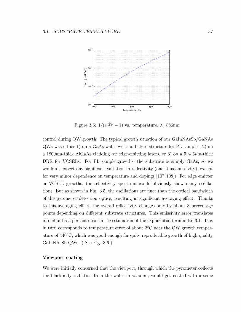
3.1. SUBSTRATE TEMPERATURE 37
400 450 500 550 60010
−11
10−10
10−9
10−8
Temperature(oC)
1/(e
xp(h
c/λk
T)−
1)
Figure 3.6: 1/(ehc
λkT − 1) vs. temperature, λ=886nm
control during QW growth. The typical growth situation of our GaInNAsSb/GaNAs
QWs was either 1) on a GaAs wafer with no hetero-structure for PL samples, 2) on
a 1800nm-thick AlGaAs cladding for edge-emitting lasers, or 3) on a 5 ∼ 6µm-thick
DBR for VCSELs. For PL sample growths, the substrate is simply GaAs, so we
wouldn’t expect any significant variation in reflectivity (and thus emissivity), except
for very minor dependence on temperature and doping( [107,108]). For edge emitter
or VCSEL growths, the reflectivity spectrum would obviously show many oscilla-
tions. But as shown in Fig. 3.5, the oscillations are finer than the optical bandwidth
of the pyrometer detection optics, resulting in significant averaging effect. Thanks
to this averaging effect, the overall reflectivity changes only by about 3 percentage
points depending on different substrate structures. This emissivity error translates
into about a 5 percent error in the estimation of the exponential term in Eq.3.1. This
in turn corresponds to temperature error of about 2oC near the QW growth temper-
ature of 440oC, which was good enough for quite reproducible growth of high quality
GaInNAsSb QWs. ( See Fig. 3.6 )
Viewport coating
We were initially concerned that the viewport, through which the pyrometer collects
the blackbody radiation from the wafer in vacuum, would get coated with arsenic

38 CHAPTER 3. ADVANCES IN GAINNASSB GROWTH
over time, leading to a lower signal level and hence lower apparent temperature read-
ing. Although this is theoretically, and also practically possible in MBE or MOVPE
chambers, we didn’t notice any systematic drift in the temperature measurement
over a very long period of 3 years, without any recalibration. The viewport is heated
to minimize arsenic deposition, and the exponential nature of the blackbody curve
means that even a few percent increase in radiation loss by the viewport corresponds
to only 1 or 2oC of temperature measurement error. Even if viewport coating did
affect pyrometry, it could be easily solved by recalibrating on a regular basis.
We were also concerned that the radiation from the heated viewport might swamp
the radiation from the wafer, but this was in practice no problem, because the view-
port temperature is much lower than the growth temperature and the detection optics
are focused on the wafer.
Wafer wobble, heater radiation leakage, and reflections from other heat
sources
As discussed above, wafer wobble was a serious problem when we tried to measure and
compensate for emissivity changes on the fly. On the other hand, without emissivity
compensation, we found wafer wobble was less problematic, because measurement of
radiation is less sensitive to wafer wobble than measurement of reflectivity. There are
two reasons for that; 1) Blackbody radiation is less directional than the focused LED
beam used for the reflectivity measurement, and 2) light has to make only a one-way
trip from the wafer to the detector for a blackbody radiation measurement, compared
to the round-trip required for a reflectivity measurement ( i.e., from the LED in the
pyrometer, via the wafer, and back to the pyrometer).
However, temperature measurements still showed periodic fluctuations when the
wafer was rotating, as shown in Fig. 3.7, for a 3-inch GaAs wafer. The amplitude of
this fluctuation was different for different wafers, and the most dominant effect was
from the size of the wafer. The fluctuation was larger for smaller wafers, as shown in
Fig. 3.7, Fig. 3.8 and Fig. 3.9. The source of these fluctuations was determined to
be the leakage of substrate heater radiation around the edges of the wafer. Fig. 3.10
shows a schematic of different wafer sizes on the wafer holder. 2-inch or quarter 3-inch

3.1. SUBSTRATE TEMPERATURE 39
51 52 53 54 55
566
567
568
569
Time(minutes)
Mea
sure
d te
mpe
ratu
re(o C
)
Figure 3.7: Pyrometer measurement fluctuations for a 3-inch wafer
16 17 18 19 20 21 22
563
564
565
566
567
568
Time(minutes)
Mea
sure
d te
mpe
ratu
re(o C
)
Figure 3.8: Pyrometer measurement fluctuations for a 2-inch wafer

40 CHAPTER 3. ADVANCES IN GAINNASSB GROWTH
52 53 54 55
560
565
570
Time(minutes)
Mea
sure
d te
mpe
ratu
re(o C
)
Figure 3.9: Pyrometer measurement fluctuations for a quarter of 3-inch wafer
wafers have gaps around the edges, through which one can clearly see the orange glow
of the substrate heater. As the detection optics of the pyrometer has a finite spot
size on the wafer, it is not surprising that this heater radiation is also captured by
the pyrometer, causing a periodic perturbation in measurement as the wafer rotates.
As further evidence of leakage, the fluctuations are much larger during wafer heat-up
as the heater is hotter, compared to during cool down, as shown in Fig. 3.11. A full
3-inch wafer also leaves a small gap around its major flat, so it also exhibits similar
fluctuations, although smaller in amplitude. The magnitude of these fluctuation was
at most ±1oC for 3-inch wafers, or ±2oC for 2-inch wafers, which was good enough
for reproducible growth of GaInNAsSb QWs. Fluctuations for quarter 3-inch wafers
were found to be too large for reliable growth, sometimes being larger than ±5oC.
Measurement wavelength was also found to be a critical choice for pyrometry.
We initially used 980nm as the detection wavelength, but this turned out to be a
poor choice, because GaAs is transparent at this wavelength up to around 400oC,
allowing the substrate heater radiation to pass through the wafer, thus swamping the
blackbody radiation from the wafer itself. We finally chose 886nm, for which GaAs
turns opaque at approximately 100oC, which is sufficiently lower than our QW growth
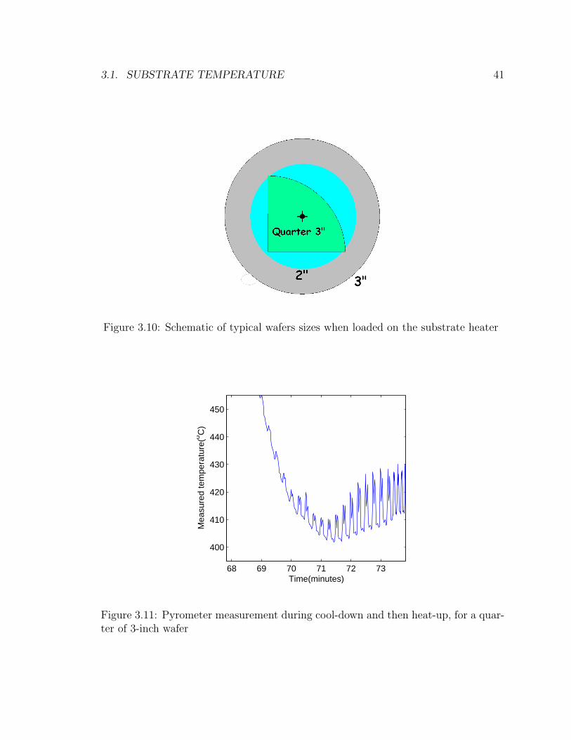
3.1. SUBSTRATE TEMPERATURE 41
Figure 3.10: Schematic of typical wafers sizes when loaded on the substrate heater
68 69 70 71 72 73
400
410
420
430
440
450
Time(minutes)
Mea
sure
d te
mpe
ratu
re(o C
)
Figure 3.11: Pyrometer measurement during cool-down and then heat-up, for a quar-ter of 3-inch wafer

42 CHAPTER 3. ADVANCES IN GAINNASSB GROWTH
temperature of 440oC.
Reflected radiation from other heat sources in the chamber can also affect py-
rometry. Effusion cells, especially the gallium cell, can be as hot as 1000oC during
growth. The cracker section of the arsenic cell is at 850oC even in the idle state.
This is much hotter than the wafer during growth, and their blackbody radiation
is larger by several orders of magnitude. Some of this radiation is captured by the
pyrometer after reflections in the chamber, limiting the minimum temperature that
the pyrometer can measure. Although the intrinsic capability of the pyrometer (when
the detector noise is compared to blackbody radiation) has no problem measuring as
low as 300oC, reflected radiations from hot cells prevented the pyrometer from read-
ing lower temperatures than 360oC , even when the wafer was at room temperature.
Fortunately, this was sufficiently lower than our typical growth temperature that this
technique proved useful.
Implications for temperature control
Despite these difficulties as discussed above, pyrometry proved to be a useful technique
with a reasonable accuracy of ± a few degrees Celcius. It was also much faster, more
convenient, and more versatile compared to the band-edge absorption method, which
required several hours of measurement for each wafer and worked only for bare SI
wafers. Pyrometry is also much more accurate than the thermocouple, which could
be off by 100 or even 200oC.
Pyrometry also allowed us to discover a few more interesting characteristics of
wafer heating in the MBE chamber.
First, different wafers may heat up at completely different rates and efficiency.
Especially dominant is the effect of wafer doping. Undoped wafers require much
higher thermocouple temperature and higher heater power than doped wafers. Un-
doped wafers are also much slower to heat than doped wafers. When we increase
the temperature setpoint, undoped wafers tend to take several minutes to reach the
setpoint, following a smooth curve. On the other hand, doped wafers heat up very
quickly overshooting by a large amount (as much as 50oC), and then settle down to
the setpoint temperature. Typical trajectories of wafer temperatures during heat-up

3.1. SUBSTRATE TEMPERATURE 43
0 2 4 6 8
440
460
480
500
520
540
560
Time(minutes)
Mea
sure
d te
mpe
ratu
re(o C
)
Figure 3.12: Pyrometer measurement during heat-up, for a 3-inch n-type wafer. Smallbumps are due to wafer tilting for easier RHEED observation
are shown in Fig. 3.12 and Fig. 3.13. This difference shows that the wafer is heated
mainly by absorbing the radiation from the heater, rather than by heat conduction.
It also shows that we have to be very careful and patient when determining the deox
temperature, because the wafer temperature might still be in a transitory state if we
don’t allow the wafer enough time to stabilize at a given temperature.
The second important finding is that the GaAs oxide desorption temperature is
indeed very constant and reliable. We observed a very similar temperature reading
(within a few degrees) on the pyrometer as the oxide desorbs from the wafer, regard-
less of wafer type, size, and vendor. We did doubt in the past whether the deox
temperature was really constant because we saw no consistency in the TC reading
at the deox temperature [56], but pyrometry enabled us to finally use this reference
with confidence.
It was also found that the TC reading offset between the deox and the QW growth
temperatures were quite repeatable, although each of them varied a lot in TC reading,
wafer to wafer. Fig. 3.14 shows the thermocouple readings at the deox(580oC) and the
QW growth(440oC) temperatures, for several 3” n-type wafers. The deox temperature
was determined by inspecting RHEED in the sys4, and the QW growth temperature

44 CHAPTER 3. ADVANCES IN GAINNASSB GROWTH
4 6 8 10 12
420
440
460
480
500
520
Time(minutes)
Mea
sure
d te
mpe
ratu
re(o C
)
Figure 3.13: Pyrometer measurement during heat-up, for a 3-inch undoped wafer
sys4 TC deox B-250 sys5 TC QWn740 747 497 468n743 750 500 469n745 745 495 469n748 756 506 473n788 777 527 499n789 777 527 497n789 775 525 494n790 760 510 478
440
460
480
500
520
540
n740
n743
n745
n748
n788
n789
n789
n790
Wafers
Therm
ocouple
readin
g(˚
C)
sys4 TC at deox - 250
sys5 TC at QW growth
Figure 3.14: TC readings at deox in sys4 and at QW growth in sys5

3.2. IMPROVEMENT IN ANNEALING CONDITIONS 45
was determined by pyrometry in the sys5. The difference in thermocouple reading
between the two temperatures was consistently very close to 280oC, even though the
two temperatures were measured in two different chambers. It was also found that the
thermocouple readings from the two chambers at deox temperature were 50oC apart
from each other. From then on, we decided to grow QWs at 230oC lower than the
sys5 deox temperature by thermocouple reading, or equivalently, 280oC lower than
the sys4 deox temperature by thermocouple reading. For full 3” n-type wafers, we
checked the pyrometer reading during growth as well, to make sure the temperature
was correct, and we didn’t experience any unexpected deviation. For quarter 3” n-
type wafers, we used the same method, only putting less weight on the pyrometer
reading due to its higher error for smaller wafers. Using this method, we grew quite
a few PL samples on quarer 3” n-type wafers and they showed very repeatable PL
intensity and wavelength. Though we have not estabilished whether a similar method
can be used for undoped or p-type wafers, establishing this relationship for n-type
wafers was sufficient for the purposes of this thesis, as the PL samples and the lasers
only required n-type wafers.
3.2 Improvement in annealing conditions
Dilute nitride materials typically have quite a large number of defects as-grown, due
to low N solubility in GaAs or InGaAs [21,22] , and in the case of MBE growth, from
the ion-related damage from the rf plasma cell [29]. Post-growth annealing has been a
standard process for dilute nitrides to remove as-grown defects and improve material
quality [109] and there have been many reports about the annealing properties [65,
72,77,85,110–114].
The annealing experiments have been done by two different methods: One is
to anneal the as-grown samples in the growth chamber(in-situ) or a furnace for a
relatively long time (tens of minutes) with arsenic fluxes supplied to suppress arsenic
desoprtion from the sample surface [113]. The second is to anneal the samples in
an RTA chamber for a short time (up to a few minutes), with a GaAs cap wafer to
minimize arsenic desorption [72, 111, 112, 114, 115]. It may seem natural to wonder
46 CHAPTER 3. ADVANCES IN GAINNASSB GROWTH
which annealing method produces a better quality after annealing, but for some
unknown reasons, most research groups tended to stick to one method rather than
comparing the two and choosing the better one. Our group was no exception in this
respect, sticking to 1-minute annealing at a few different temperatures in an RTA. We
were able to achieve very low threshold for 1.55µm GaInNAsSb lasers [52] by using
1-minute annealing, but this doesn’t necessarily mean that it is the best that could
be achieved.
For silicon CMOS processing, it is well known that short-duration high-temperature
annealing is better than long-duration low-temperature annealing because the defect
annealing effects have stronger temperature dependence than the undesirable tran-
sient enhanced diffusion(TED). We were interested in finding out whether GaInNAsSb
QWs follow an analogous or an opposite trend. In the case of dilute nitrides, there are
two distinct processes affecting the material quality during annealing: one is removal
of growth-induced defects and the other is creation of annealing-induced defects [77].
Comparison of temperature dependencies of the two processes would reveal whether
short-duration high-temperature annealing or long-duration low-tempature annealing
results in higher material quality.
To determine the temperature dependencies of annealing processes, we annealed
GaInNAsSb PL samples using various temperatures and durations. A PL sample has
a 7.5nm-thick Ga0.62In0.38N0.03As0.943Sb0.027 QW with 21nm GaN0.04As0.96 barriers on
both sides, after growing 300nm updoped GaAs buffer layer and is followed by a
50nm GaAs layer. The GaAs layers are grown at 580oC and the QW is grown at
440oC with V/III BEP(beam equivalent pressure) ratio of 20. This is nominally the
same composition and growth condition as those QWs used for our lowest threshold
1.55µm GaInNAsSb lasers as reported in [52]. It is important to use high quality
QWs as in this study to make sure that the intrinsic property of GaInNAsSb QWs is
not obscured by extrinsic behaviors due to an unnecessarily high level of defects, as
the level of defects can affect the annealing properties significantly [87,88].
Figure 3.15 shows the peak photopluminescence(PL) intensity and wavelength
after annealing GaInNAsSb PL samples for 1-minute in the RTA. As previously re-
ported by many researchers, the PL intensity initially increases with temperature as

3.2. IMPROVEMENT IN ANNEALING CONDITIONS 47
0
0.2
0.4
0.6
0.8
1
1.2
700 750 800 850Annealing Temperature (oC)
PL
Inte
nsity
(A.U
.)
1520
1540
1560
1580
1600
1620
700 750 800 850
Annealing Temperature (oC)
PL
peak
wav
elen
gth(
nm)
(a) PL peak Intensity (b) Peak wavelength
Figure 3.15: Result of 1-minute annealing at different temperatures forGa0.62In0.38N0.03As0.943Sb0.027 QW
growth-induced defects are annealed, but starts to degrade when the temperature
gets too high. The optimum occurs around 780oC. The wavelength becomes shorter
as the QW is annealed at higher temperatures. The mechanism of the blueshift was
initially hypothesized to be indium [79, 80, 116] or nitrogen [3, 23] outdiffusion from
the quantum wells, but later research indicated that the change in nearest-neighbor
configuration of nitrogen atoms explains most, if not all, of this effect [85]. In Fig.
3.15, the PL intensity is normalized with respect to the optimum at 780oC, and this
optimum intensity is used as the reference for the annealing and growth studies in
this and following sections.
The first experiment was to anneal the same PL samples at 700oC, for 10 to 150
minutes, as shown in Fig. 3.16. The 700oC result resembles that in Fig. 3.15, in that
the PL intensity initially increases and then eventually decreases when annealed too
long or too hot. But unlike Figu. 3.15, Fig. 3.16 shows a very wide window of flat
PL intensity(as long as 2 hours), and the peak PL intensity is more than two times
higher than the 1-minute annealed samples. Note that a similar wide plateau was
also observed in [65], where the PL intensity improvement saturates after about 5

48 CHAPTER 3. ADVANCES IN GAINNASSB GROWTH
1450
1500
1550
1600
1650
1700
0 40 80 120 160Minutes
Wav
elen
gth(
nm)
740C720C700C
(a) PL peak Intensity (b) Peak wavelength
0.0
1.0
2.0
3.0
0 40 80 120 160Minutes
Inte
nsity
(A.U
.)
740C720C700C
Figure 3.16: PL intensity and wavelength vs. annealing duration forGa0.62In0.38N0.03As0.943Sb0.027 QW.
minutes and stays flat up to 30 minutes. [65]. But eventual degradation after 2 hours
of apparent stability of material quality was not reported in [65] or any other reports,
to the best of our knowledge.
Such a long stability plateau and the following degradation is a very interesting
behavior in itself, and the higher PL intensity compared to 1-minute annealing is also
very intriguing. Additionally, at 700oC, the over-anneal degradation does not begin
until the sample is annealed more than 2 hours. On the other hand, a 1-minute anneal
at 800oC was enough to generate annnealing-induced defects, as shown in Fig. 3.15.
This implies that the annealing-induced degradation has a very steep temperature
dependence, or equivalently, a large activation energy. To examine the temperature
dependence of the annealing-induced degradation, we next annealed samples at 720oC
and 740oC until substantial degradation was observed, and the result is also shown
in Fig. 3.16. While it took as long as 150 minutes until the onset of degradation at
700oC, it took only 60 minutes at 720oC, and only about 10 minutes at 740oC. This
is roughly ×3–×5 difference for every 20oC, which in turn translates into activation
energy of 6–7eV assuming an Arrhenius relationship.
On the other hand, removal of growth-induced defects was found to have a much

3.2. IMPROVEMENT IN ANNEALING CONDITIONS 49
(a) PL peak Intensity (b) Peak wavelength
0
1
2
3
0 20 40 60Minutes
Inte
nsity
(A.U
.)
680C700C720C
1480
1520
1560
1600
1640
0 20 40 60Minutes
Wav
elen
gth(
nm)
680C700C720C
Figure 3.17: PL intensity and wavelength vs. annealing duration forGa0.62In0.38N0.03As0.943Sb0.027 QW.
shallower temperature dependence than that of annealing-induced defect generation.
Figure 3.17 shows the result of annealing experiments at 680–720oC. The PL intensity
saturates after about 40 minutes of 680oC annealing, whereas it takes 30 and 10
minutes at 700oC and 720oC respectively for the PL intensity to saturate. This
temperature dependence is about ×2 faster per 20oC increase, which translates into
activation energy of about 3eV.
Due to this combination of a shallow temperature dependence for removal of
growth-induced defects, and the steep temperature dependence of annealing-induced
degradation, longer and cooler anneals produce not only higher but also more repro-
ducible PL intensity than shorter and hotter anneals, because the lower temperature
inhibits the degradation process more significantly than it slows the improvement
process. The optimum intensity that can be achieved with long anneals at 700oC
was indeed about ×2 higher than our previous best for 1-minute anneals. (Compare
Figs. 3.15 and 3.16. Their PL intensities are plotted in the same scale, so that direct
comparison is possible.) This higher PL intensity by low-temperature long-duration
annealing implies better material quality, which in turn can produce better laser
results. In addition, low-temperature, long-duration annealing allows a very wide

50 CHAPTER 3. ADVANCES IN GAINNASSB GROWTH
(a) Removal of growth-induced defects (b) Degradation induced by annealing
0
5
10
0 20 40 60 80
Minutes
PL
Inte
nsity
(A.U
.)
660C680C700C
0
5
10
0 5 10 15 20 25
Minutes
PL
Inte
nsity
(A.U
.)
620C640C660C
Figure 3.18: PL intensity vs. annealing duration for Ga0.7In0.3N0.012As0.968Sb0.02 QW.
optimum processing window, which significantly improves process control.
Similar experiments were done for a significantly different QW composition, namely
7nm-thick Ga0.7In0.3N0.012As0.968Sb0.02 QW, for 1.26µm emission after anneal(1.31µm
before anneal). The result is shown in Fig. 3.18. We can see a very similar trend
as in Figs. 3.16 and 3.17. The PL intensity degradation by annealing-induced de-
fects have a steep temperature dependence, exhibiting a widely different behavior for
only 40oC difference in the annealing temperature. Compared to that, the removal
of growth-induced defects show a much shallower temperature dependence.
Another kind of PL samples with a completely different structure was also an-
nealed and measured, namely 150-nm thick Ga0.92In0.08N0.02As0.98. This is a lattice-
matched thick layer with light emission at 1.15µm, rather than a strained QW. It
has no Sb and only 5nm GaAs cap layer, unlike the other two kinds of PL samples
discussed above, which had Sb incorporation and 50nm cap layers. Despite these
differences, Fig.3.19 shows a similarly shallow temperature dependence for the re-
moval process of growth-induced defects, namely roughly ×4 every 40oC, which is
equivalent to ×2 every 20oC. On the other hand, we were not able to extract mean-
ingful temperature dependence for the creation of annealing-induced defects due to
rather noisy result as shown in Fig.3.19(b) and insufficient amount of samples left for

3.2. IMPROVEMENT IN ANNEALING CONDITIONS 51
0
0.05
0.1
0.15
0.2
0 20 40 60
Minutes
PL
inte
nsity
(A.U
.)
700C740C780C
0
0.05
0.1
0.15
0 5 10 15 20
Minutes
PL
Inte
nsity
(A.U
.)
820C840C
(a) Removal of growth-induced defects (b) Degradation induced by annealing
Figure 3.19: PL intensity vs. annealing duration for lattice-matched 150nm-thickGa0.92In0.08N0.02As0.98 layer.
measurment. However, this result still agrees with those of the other two samples in
that the lower-temperature annealing results in roughly ×2 higher PL intensity than
higher-temperture annealing for a short duration. ( PL intensities of Fig.3.19(a) and
(b) can be directly compared with each other. )
These measurements indicate that different alloys of GaInNAs(Sb) exhibit similar
dependence on annealing temperatures, even for vastly different compositions and
thicknesses. This implies that the same defect removal and defect creation mecha-
nisms are in action during annealing for any GaInNAs(Sb) compositions, which is
not surprising since this annealing behavior is unique to the dilute nitride materials
and is definitely closely associated with their unique growth conditions due to the low
solubility of nitrogen.
On the other hand, the improvement and degradation processes by annealing are
observed at widely different temperatures depending on the composition, as reported
by many researchers [72,85,112,114,115]. This indicates that the PL degradation from
over-annealing does not arise from arsenic vacancies from the surface or elsewhere in
the substrate, because the annealing temperature and duration at which the arsenic
vacancies reach the GaInNAs(Sb) layer would not depend much on its composition.

52 CHAPTER 3. ADVANCES IN GAINNASSB GROWTH
Outdiffusion from the QW [77] was also suggested as a cause of PL degradation from
over-annealing, but apparently this is not the case either, as the interdiffusion process
has been reported to have an activation energy of about 3eV [89, 110, 117], which is
significantly smaller than the activation energy of annealing-induced defects as dis-
cussed above. A 6–7eV activation energy is observed for annealing-induced defects
for our GaInNAs(Sb) QW samples, which is rather large for point defects, so we
suspect it is more likely to be associated with extended defects, i.e. dislocations. Ac-
tual observation of dislocations was reported in [77] using TEM(transmission electron
microscopy), but more research is needed to fully understand the mechanism of the
annealing-induced defects.
The wavelength blueshift is another important process that happens during an-
nealing. It is now known that a large portion of the blueshift is due to the nearest-
neighbor reconfiguration of nitrogen atoms, and the activation energy of the reconfig-
uration process is quite low (∼0.6eV) [85, 117]. This reconfiguration happens rather
quickly during the initial phase of annealing, and then additional blueshift due to
interdiffusion and its activation energy of about 3eV is reported [110, 117]. Our
wavelength measurements in Figs. 3.17 and 3.16 qualitiatively agree with these re-
ports with very rapid initial blueshift commensurate with the low activation energy
of ∼0.6eV, and very small, if any, additional blueshift agreeing with the higher acti-
vation energy of ∼3eV. However, the additional blueshift due to interdiffusion is so
small compared to the initial large blueshift due to nearest-neighbor reconfiguration
that it can be practically ignored for device applications.
The most important implication of this annealing experiment for this thesis work is
that about ×2 higher PL quailty can be achieved by annealing at lower temperatures
for longer durations, instead of the traditional 1-minute annealing. In addition, the
PL intensity stays high for a very wide window of annealing durations, making the
process far easier to control.

3.3. IMPROVEMENT BY LOWER GROUP-V FLUX 53
300 400 500 600 700 800 900 100010
-25
-20
-15
-10
10-5
MBE Window
x=0.02, y=1
x=0.02, y=0.7
Temperature (°C)
phase segregation
no phase segregation
p GaG
(pA
s2G)1/
2 (m
bar3/
2 )
10
10
10
Figure 3.20: Ga and As equivalent pressures for which segregation-free growth hap-pens for GayIn1−yNxAs1−x [3]
3.3 Improvement by Lower group-V flux
Early theoretical and experimental work proposed that low growth temperatures and
high arsenic fluxes were required for single phase molecular beam epitaxy (MBE)
of dilute nitride materials [3, 118], as shown in Fig.3.20. Following these growth
guidelines, we were able to realize low threshold 1.5µm GaInNAsSb lasers by growing
at relatively low temperatures ( 440oC) and high group-V fluxes (×20 V/III ratio in
BEP(beam equivalent pressure)) [52]. On the other hand, significant improvement
in material quality for Sb-free GaInNAs was reported when grown at a much lower
arsenic flux(only ×1.2 of group-III flux) and also much lower temperature(350oC) [5].
This result does not contradict with the growth regime illustrated in Fig.3.20 as
lower temperature does allow lower arsenic pressure, but it draws our attention to
the fact that the analysis underlying Fig.3.20 [3] only deals with the avoidance of
phase segregation, and thus does not actually specify exactly which growth condition
to choose in the wide parameter range that allows segregation-free growth. Low
temperature and high arsenic flux prevents phase segregation, but on the other hand it
may reduce the surface mobility too much by limiting arsenic re-evaporation, leading

54 CHAPTER 3. ADVANCES IN GAINNASSB GROWTH
Figure 3.21: PL results for GaInNAsSb QWs, as a function of the As/III flux ratio
to undesirable excess As point defects. As this possibility was not explicitly explored,
it seemed likely that the high arsenic flux growth previously considered optimum was
not actually the best achievable.
We first examined the possibility by trying different arsenic fluxes at 440oC, the
result of which is shown in Fig.3.21 and reported in [76]. The graph is shown in terms
of actual As/III flux ratio, which is about half of the BEP(Beam Equivalent Pressure),
and the sample with the heighest As/III ratio in the graph corresponds to the As/III
BEP ratio of 20. From this result, 440oC and x20 As/III BEP ratio actually is
the optimum, with the PL intensity decreasing slowly as the ratio is lowered, before
dropping precipitously as the flux ratio drops below 3. On the other hand, the
wavelength becomes longer as we lower the arsenic flux, which is probably due to
increased antimony incorporation as the Sb/As ratio increases with lower As flux. In
addition to wavelength change, the Sb/As ratio is also known to affect the growth
quality as shown in Fig.3.22 [4], so it is very possible that changing the As flux alone
is not the best way to explore the growth parameters.
Therefore, we instead set out to change the As and Sb fluxes together, while
keeping their ratio constant. We grew 1.55µm PL samples at various (As+Sb/)/III

3.3. IMPROVEMENT BY LOWER GROUP-V FLUX 55
Figure 3.22: PL results versus Sb flux from [4]
flux ratios at two different growth temperatures. The first set of samples were grown
with 39% indium with the (As+Sb)/III flux ratios ranging from ×11 to ×20 in BEP
ratio (roughly ×5.5 to ×10 in real flux ratio) at 410oC. The ratio between arsenic
and antimony fluxes was fixed at 54 in BEP, and the nitrogen plasma was also kept
constant, with the same gas flow and power. Another set of similar PL samples
was grown at 410oC, under (As+Sb)/III ratios ranging from ×3 to ×11. And the
third set of PL samples was grown at 440oC with (As+Sb)/III ratios between ×2 and
×15. This first set was grown about 18 months before the other two samples, and its
results were reported earlier in [76]. During the 18 months, the MBE chamber was
not operational going through significant repairs and maintenance, and the nitrogen
plasma cell was operating under a significantly different condition after the repairs, as
described in the previous chapter. Despite the significant lapse of time and different
chamber condition, the results of all three sets of growths align with one another
reasonably well, which is a good sign for the repeatability of GaInNAsSb growth.
Figure 3.23 shows the peak PL intensity after 1-minute annealing for the first set
of samples (Growth T=440oC). Figure 3.24 shows the peak PL intensity for all the
three sets of samples. ( note: The result for ×2 flux ratio grown at 440oC is not

56 CHAPTER 3. ADVANCES IN GAINNASSB GROWTH
0
0.5
1
1.5
2
640 660 680 700 720 740
Anneal temperature(°C)
PL in
tens
ity (A
.U.)
(As+Sb)/III=4(As+Sb)/III=7(As+Sb)/III=9(As+Sb)/III=11(As+Sb)/III=15
Figure 3.23: PL intensity for different (As+Sb)/III flux ratios annealed for 1 minute
0
0.5
1
1.5
2
0 5 10 15 20
(As+Sb)/III flux ratio (BEP)
Peak P
L inte
nsity (
A.U
.)
410˚C growth, 2nd attempt
410˚C growth, 1st attempt
440˚C growth
Figure 3.24: PL intensity at the optimum annealing temperature vs. (As+Sb)/IIIflux ratio. Annealed for 1 minute

3.3. IMPROVEMENT BY LOWER GROUP-V FLUX 57
0.0
0.5
1.0
1.5
2.0
2.5
1.0 1.2 1.4 1.6 1.8 2.0 2.2V/III flux ratio
PL
inte
nsity
[a.u
.]
1450
1460
1470
1480
1490
1500
1510
1520
1530
1540
1550
Wavelen
gth(nm
)
Wavelength
PL Intensity
Figure 3.25: PL peak intensity(solid circles) and wavelength(open circles) versusAs/III ratio [5]
shown because the sample was optically inactive.)
The most important point from this result is that much higher PL intensity (∼ ×2)
is achieved by lowering As and Sb fluxes together. It is to be noted that the PL
intensity graphs are normalized with respect to the peak intensity we achieved under
the growth condition of ×20 flux ratio and 440oC and 1-minute annealing, which was
previously considered optimal.
And there is an optimum flux ratio, which varies depending on the growth tem-
perature. Fig.3.24 shows that both too high and too low fluxes result in sub-optimal
PL intensity, with an optimum flux ratio of about 9 when grown at 440oC. On the
other hand, the optimum flux ratio is either 2 or even lower at 410oC. Both growth
temperatures give similar optimum PL intensity, but we chose to use 440oC as the
growth temperature, because the optimum V flux is too low (close to 1 in real V/III
flux ratio) for the 410oC growth, and the growth quality would be too sensitive to the
group-V flux control as shown in Fig.3.25 [5]. There is also less concern about the
controllability of the arsenic flux when grown at 440oC, because the adjacent GaNAs
layers are grown at a (As+Sb)/III BEP ratio of 15, which is much higher than the low
flux required for 410oC growth of GaInNAsSb, but closer to ×9 required for 440oC

58 CHAPTER 3. ADVANCES IN GAINNASSB GROWTH
growth. Temperature control is also easier at 440oC, as the pyrometer noise floor is
too high for good control at 410oC, and the required temperature change from the
580o for adjacent GaAs layers is smaller for 440oC.
The trend of lower optimal flux for lower growth temperature can be easily un-
derstood from the conventional tradeoffs in MBE growth conditions, whereby either
high growth temperature or low group-V flux leads to excessive surface desorption
or phase segregation, while growth at too low temperature or too high group-V flux
impedes atoms from reaching the correct lattice sites. The effect of antimony flux
is especially important, as it is a reactive surfactant, which improves the quality of
epitaxy by inhibiting the surface diffusion length [90] when the epitaxial layer is either
strained or has a large miscibility gap, both of which are true for GaInNAsSb grown
on GaAs [21,22]. As the antimony flux has a strong influence on the surface diffusion
properties, reduction of Sb flux together with As flux was critical to improving the
material quality in this report, while no improvement was observed if only the As
flux was changed. On the other hand, the other group-V element, nitrogen, showed
no measurable variation in composition as determined by SIMS over the samples in
this study, despite the huge variation in the As and Sb fluxes. This insensitivity of N
incorporation to other group-V fluxes agrees with our previous finding that nitrogen
behaves more like a group-III element as far as composition control is concerned, and
its composition is mainly dependent on the growth rate, which is determined by the
group-III fluxes [23].
Figure 3.26 shows a dependence of wavelength on the (As+Sb)/III ratio, where the
wavelength tends to decrease as the flux ratio approaches the optimum ratio for high
PL intensity. Although it might be possible that antimony incorporation increases
slightly under high Sb and As fluxes and nitrogen incorporates more under low Sb
and As fluxes, the acutal SIMS results shown in 3.28 do not support this hypothesis.
No significant difference was found in the HRXRD measurements either, as shown in
Figure 3.27 for 440oC growths. The HRXRD scans show very similar high structural
qualities and the strains do not show any discernable difference. We were not able to
determine the mechanism of the wavelength dependence, but shorter wavelength for
the optimum PL intensity was repeatedly observed. Therefore, we tried to increase

3.3. IMPROVEMENT BY LOWER GROUP-V FLUX 59
1480
1500
1520
1540
1560
0 5 10 15 20
(As+Sb)/III ratio in BEP
Peak P
L w
ave
length
(nm
)
410˚C growth, 2nd attempt
410˚C growth, 1st attempt
440˚C growth
Figure 3.26: PL wavelength for different (As+Sb)/III flux ratios. Annealed for 1minute
30.5 31 31.5 32 32.5 33 33.5 34
10−5
100
105
ω/2θ (degrees)
Cou
nts(
A.U
.)
4x
7x
11x
9x
15x
GaInNAsSb QW GaNAs
Figure 3.27: XRD result for different (As+Sb)/III flux ratios, grown at 440oC
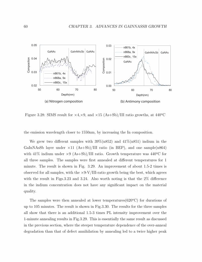
60 CHAPTER 3. ADVANCES IN GAINNASSB GROWTH
0.02
0.03
0.04
0.05
50 60 70 80
Depth(nm)
Com
posi
tion
n861b, 4xn868a, 9xn860c, 15x
0.00
0.01
0.02
0.03
50 60 70 80
Depth(nm)
Com
posi
tion
n861b, 4xn868a, 9xn860c, 15x
(a) Nitrogen composition (b) Antimony composition
GaNAs GaInNAsSb GaNAs GaInNAsSb GaNAs
GaNAs
Figure 3.28: SIMS result for ×4,×9, and ×15 (As+Sb)/III ratio growths, at 440oC
the emission wavelength closer to 1550nm, by increasing the In composition.
We grew two different samples with 39%(n852) and 41%(n851) indium in the
GaInNAsSb layer under ×11 (As+Sb)/III ratio (in BEP), and one sample(n864)
with 41% indium under ×9 (As+Sb)/III ratio. Growth temperature was 440oC for
all three samples. The samples were first annealed at different temperatures for 1
minute. The result is shown in Fig. 3.29. An improvement of about 1.5-2 times is
observed for all samples, with the ×9-V/III-ratio growth being the best, which agrees
with the result in Figs.3.23 and 3.24. Also worth noting is that the 2% difference
in the indium concentration does not have any significant impact on the material
quality.
The samples were then annealed at lower temperatures(620oC) for durations of
up to 105 minutes. The result is shown in Fig.3.30. The results for the three samples
all show that there is an additional 1.5-3 times PL intensity improvement over the
1-minute annealing results in Fig.3.29. This is essentially the same result as discussed
in the previous section, where the steeper temperature dependence of the over-anneal
degradation than that of defect annihilation by annealing led to a twice higher peak

3.3. IMPROVEMENT BY LOWER GROUP-V FLUX 61
0
0.5
1
1.5
2
2.5
640 660 680 700 720 740
Anneal temperature(°C)
PL
inte
nsity
(A.U
.)
n851, 41% In, (As+Sb)/III=11
n852, 39% In, (As+Sb)/III=11
n864, 41% In, (As+Sb)/III=9
Figure 3.29: PL result for low As+Sb flux growths, after one-minute annealing
0
0.5
1
1.5
2
2.5
3
3.5
4
4.5
5
5.5
0 20 40 60 80 100
Anneal duration (minutes)
PL
inte
nsity
(A.U
.)
n851, 41% In, (As+Sb)/III=11n852, 39% In, (As+Sb)/III=11n864, 41% In, (As+Sb)/III=9
Figure 3.30: PL result for low As+Sb flux growths, after long annealing

62 CHAPTER 3. ADVANCES IN GAINNASSB GROWTH
n+ G aAs S ubs trate
p
i
n
Quantum W ells
Lower mirror
Upper mirrorGaAs cap (50nm)GaInNAsSb/GaNAs QW
(a) PL sample (b) Edge-emitting laser (c) VCSEL
Figure 3.31: PL sample and laser structures studied for this thesis
PL intensity when annealed for a longer duration (tens of minutes) at a lower temper-
ature (60-80oC below the optimum 1-minute annealing temperature). The difference
for this study is that the samples in this study are grown under the newly-discovered
optimal (As+Sb) flux, resulting in roughly 2X better PL intensity for 1-minute an-
nealing. Therefore, the overall improvement in peak PL intensity by combining the
low group-V-flux growth and the low-temperature long-duration annealing is as much
as 3-5 times compared to our previous best samples, which were grown under high
(As+Sb) fluxes and annealed for 1-minute at higher temperatures.
3.4 Effects of self-annealing
Self-annealing refers to the inevitable in-situ annealing that the QW experiences
during growth of actual devices, such as edge-emitting lasers, photo detectors, or
VCSELs, because it takes from tens of minutes to several hours to grow the upper
structures above the QWs [111,119]. Figure 3.31 shows the three different structures
that were grown and studied for this work. PL samples have a 50nm GaAs cap layer,
which takes 10–15 minutes. On the other hand, it takes about 2.5 hours to grow the
upper cladding for an edge-emitter, and more than 6 hours to grow the upper DBR
for a VCSEL. The growth temperature is 580oC for all these upper structures for PL

3.4. EFFECTS OF SELF-ANNEALING 63
(b) Ex-situ annealing behavior for high-In QW after upper-cladding growth
(a) Room-temperature pulsed L-I curve for lasers based on two di�erent active regions
Figure 3.32: Laser result and PL for high-indium QW
samples or laser structures.
10–15 minutes of self-annealing during PL sample growth has not been an issue for
the study of GaInNAsSb material, as the PL improvement and blueshift due to the
self-annealing seem neglible compared to those due to the additional ex-situ annealing
( For example, in Figs.3.16 and 3.17, 0-minute annealing refers to the nominally as-
grown sample, which actually experienced 10–15 minutes of self-annealing ). On
the other hand, the self-annealing has been an important factor for edge-emitters
and VCSELs. We have had to anneal edge-emitting lasers at lower temperatures
(by 20–40oC) than the ’optimum PL’ temperature [52, 96, 120]. And the previous
VCSEL operated best when no ex-situ anneal was performed [121]. However, the
self-annealing process has not been studied directly, and because of that, the search
for the right ex-situ annealing condition has been an ad-hoc blind search process
rather than a systematic one, which complicated the laser fabrication.
The need for a more explicit study of the self-annealing process was more urgently
felt when we saw poor laser performance from a QW design that showed high PL
intensity, when we were trying to achieve low threshold 1.55µm lasers for the first
time [122]. Our initial approach to increase the emission wavelength out to 1.55µm

64 CHAPTER 3. ADVANCES IN GAINNASSB GROWTH
was to increase the In composition (to 41%) to the GaInNAsSb QW. Although this
resulted in decent PL, the laser using the high-indium QW showed high threshold
current. On the other hand, increasing nitrogen while keeping In at 38% showed
similar PL intensity up to 1.55µm and enabled us to achieve the lowest-threshold
GaInNAsSb laser at 1.55µm. The dicrepancy between the good PL and the poor laser
for the high-In QW was attributed to over-annealing the QWs by the self-annealing
process, as shown in Fig. 3.32. In this experiment, an undoped laser structure is
grown using the 41%-In QW, and compared against a PL sample after 1-minute
annealing using the same QW. This structure is identical to an edge-emitting laser,
except that the AlGaAs claddings are not doped, to minimize optical loss and carrier
loss in the doped layers in order to maximize the PL signal. Fig.3.32 indicates that
the QW appears to get over-annealed after 2.5 hours of self-annealing, thus showing
decreasing PL intensity with any additional ex-situ annealing. It was hypothesized
that higher compressive strain in the QW due to additional In was responsible for
this reduced thermal stability of the 41%-In QW against self-annealing, resulting in
inferior laser performance despite decent PL quality.
In the previous section, significant improvement in PL intensity was realized by
growing QWs at lower (As+Sb) fluxes, but it came with an undesirable side effect
of slightly shorter emission wavelength. In order to extend the wavelength again, we
tried increasing the indium content to 41% despite the potential problem of reduced
thermal stability against self-annealing. Interestingly, we did not find any sign of
inferior thermal stability of a 41%-In QW compared to a 39%-In QW as shown in
Fig.3.30, which would imply that a 41%-In QW can survive the 2.5-hour self-annealing
just as well as a lower-In QW does. Though this contradicts our previous hypothesis
that a 41%-In QW is irreversibly damaged during 2.5-hour self-annealing, and the
cause of this discrepancy needs more investigation, this encouraged us to explore the
41%-In QWs further in the hope that the 41%-In QW may be thermally stable enough
to be useful for GaInNAsSb lasers.
We grew two GaInNAsSb PL samples for emission wavelength around 1.5µm, one
with 39% In and the other with 41% In. They were both grown at×9 (As+Sb)/III flux
ratio as measured in BEP(Beam equivalent pressure) and at the growth temperature
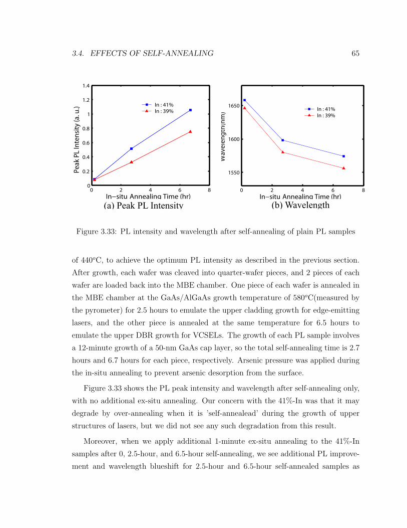
3.4. EFFECTS OF SELF-ANNEALING 65
0 2 4 6 80
0.2
0.4
0.6
0.8
1
1.2
1.4
In−situ Annealing Time (hr)
Peak
PL
Inte
nsity
(a. u
.) In : 41%In : 39%
(a) Peak PL Intensity (b) Wavelength
0 2 4 6 8
1550
1600
1650
In−situ Annealing Time (hr)
Wav
elen
gth(
nm) In : 41%
In : 39%
Figure 3.33: PL intensity and wavelength after self-annealing of plain PL samples
of 440oC, to achieve the optimum PL intensity as described in the previous section.
After growth, each wafer was cleaved into quarter-wafer pieces, and 2 pieces of each
wafer are loaded back into the MBE chamber. One piece of each wafer is annealed in
the MBE chamber at the GaAs/AlGaAs growth temperature of 580oC(measured by
the pyrometer) for 2.5 hours to emulate the upper cladding growth for edge-emitting
lasers, and the other piece is annealed at the same temperature for 6.5 hours to
emulate the upper DBR growth for VCSELs. The growth of each PL sample involves
a 12-minute growth of a 50-nm GaAs cap layer, so the total self-annealing time is 2.7
hours and 6.7 hours for each piece, respectively. Arsenic pressure was applied during
the in-situ annealing to prevent arsenic desorption from the surface.
Figure 3.33 shows the PL peak intensity and wavelength after self-annealing only,
with no additional ex-situ annealing. Our concern with the 41%-In was that it may
degrade by over-annealing when it is ’self-annealead’ during the growth of upper
structures of lasers, but we did not see any such degradation from this result.
Moreover, when we apply additional 1-minute ex-situ annealing to the 41%-In
samples after 0, 2.5-hour, and 6.5-hour self-annealing, we see additional PL improve-
ment and wavelength blueshift for 2.5-hour and 6.5-hour self-annealed samples as

66 CHAPTER 3. ADVANCES IN GAINNASSB GROWTH
600 650 700 7500
0.5
1
1.5
2
2.5
Annealing Temperature ( �C)
PL In
tens
ity (a
. u.)
600 650 700 7501480
1520
1560
1600
1640
Annealing Temperature ( �C)
Wav
elen
gth
(nm
)
0 hr(n851)2.5 hr (n851a)6.5 hr (n851b)
0 hr(n851)2.5 hr (n851a)6.5 hr (n851b)
(a) Peak PL Intensity (b) Wavelength
No ex-situAnnealing
Figure 3.34: Results of additional ex-situ 1-minute annealing of 41%-In plain PLsamples after 0-, 2.5-, and 6.5-hour self-annealing

3.4. EFFECTS OF SELF-ANNEALING 67
shown in Fig. 3.34, in the same way as we see without self-annealing. Although
longer self-annealing results in higher PL intensity and shorter wavelength for lower
ex-situ annealing temperatures, all three samples reach similar PL intensity and wave-
length for higher ex-situ annealing temperature. Moreover, longer self-annealing gives
higher optimum PL intensity, although the difference is not large. Now it seems very
clear that hours of self-annealing during edge-emitter upper-cladding growth and even
thicker VCSEL upper-DBR growth does not cause over-annealing degradation, even
for a high In content of 41%.
This is a very encouraging result, but we still had doubts because of our previous
disappointing experience with 41%-In QWs. Noticing that the PL samples differ from
actual laser structures in that PL samples do not have doped AlGaAs claddings, we
grew another PL sample with a more laser-like structure to more faithfully reproduce
the conditions that a QW is placed in during self-annealing. This laser-like PL struc-
ture is essentially an edge-emitting laser structure, only with thinner claddings for
more efficient PL measurement. It has a 500-nm thick Al0.4Ga0.6As bottom cladding
with n-type doping of 1018cm−3 and a 100-nm thick Al0.4Ga0.6As top cladding with
p-type doping of 1018cm−3, while an edge-emitter structure has 1.8µm-thick claddings
on both sides. After growth, this laser-like PL sample was cleaved into quarter wafers
and two quarters pieces were annealed for 2.5 and 6.5 hours respectively in the MBE
chamber, at the GaAs/AlGaAs growth temperature of 580oC.
The result of PL measurement for ex-situ 1-minute annealing on the self-annealed
laser-like PL samples shown in Fig.3.35 shows a very similar trend with Fig.3.34. Some
PL improvement and wavelength blueshift happens in-situ during self-annealing, but
definitely no degradation happens due to self-annealing. There is also additional PL
improvement and wavelength blueshift by ex-situ annealing, which is an indication
that the QW is not over-annealed by self-annealing, although the QW seems to have
been almost fully annealed after 6.5 hours of in-situ self-annealing. In addition, the
similarity of annealing results for laser-like PL samples (Fig.3.35) to those for plain PL
samples (Fig.3.34) implies that the observed annealing properties are truly intrinsic
properties of the QW, rather than extrinsic properties influenced by the presence of
nearby AlGaAs layers or their doping levels, or distance of the QW to the surface or

68 CHAPTER 3. ADVANCES IN GAINNASSB GROWTH
560 600 640 680 7200
1
2
3
4
5
6
Anneal te mperature( oC )
Nor
mal
ized
PL
inte
nsity
No In-s itu anneal2.5 hrs in-s itu a nneal6.5 hrs in-s itu a nneal
No ex-situ anneal
560 600 640 680 7201480
1520
1560
1600
1640
Anneal te mperature(o
C )W
avel
engt
h(nm
)
No In-s itu anneal2.5 hrs in-s itu a nneal6.5 hrs in-s itu a nneal
No ex-situ anneal
(a) Peak PL Intensity (b) Wavelength
Figure 3.35: Results of additional ex-situ 1-minute annealing on ”Laser-like” PLsamples with 41%-In QW
the substrate.
It becomes clearer that the QW is far from being fully or overly annealed even
after 6.5 hours of self-annealing, when we apply long and cool ex-situ annealing to
the samples. Fig.3.36 shows that additional 2–3 times improvement in PL inten-
sity is obtained by ex-situ annealing, even after many hours of in-situ self-annealing.
The apparent redshift of wavelength with longer annealing seems to contradict the
usual observation of blueshift under annealing, but we suspect this is due to the
non-uniformity of wavelength over the wafer. There is about 40nm difference in PL
emission wavelength between the center and the edge of a wafer, with the center emit-
ting at a longer wavelength. This particular long-annealing experiment was executed
in such a way that pieces closer to center are annealed longer. If we remove the effect
of this wavelength nonuniformity, we expect to see negligible wavelength shift after
20 minutes.
These laser-like PL samples were also useful as benchmark samples for optimizing
the annealing process for actual edge-emitting laser or VCSEL wafers. When we
grow edge-emitting lasers or VCSELs, we grow a laser-like PL sample with nominally
the same QW composition along with lasers, preferably in the same day or at least

3.4. EFFECTS OF SELF-ANNEALING 69
0 10 20 30 40 50 601460
1500
1540
1580
1620
Anneal time(min)
Wav
elen
gth(
nm)
No In−situ anneal2.5 hrs in−situ anneal6.5 hrs in−situ anneal
0 10 20 30 40 50 600
5
10
15
Anneal time(min)
Nor
mal
ized
PL
inte
nsity
No In−situ anneal2.5 hrs in−situ anneal6.5 hrs in−situ anneal
(a) Peak PL Intensity (b) Wavelength
Figure 3.36: Results of long-annealing at 620oC on laser-like PL samples with 41%-InQW
within a few days. We determined the optimal annealing temperature and duration
by annealing and measuring the laser-like PL sample, and applied the same annealing
conditions to the laser wafers. This enabled us to determine the annealing conditions
at the beginning of laser fabrication, instead of having to anneal different wafer pieces
at a few different temperatures, fabricate them all into lasers, and then pick a good
one by measuring the completed lasers. In addition, as discussed in 3.2, annealing
at lower temperatures for long durations resulted in higher PL intensity and easier
process control than the 1-minute annealing at a few randomly chosen temperatures,
which had been previously administered. The results of edge-emitting lasers and
VCSELs using the new growth and annealing conditions are presented in the following
chapters.

Chapter 4
Edge-emitting lasers
4.1 Laser structure
Edge emitting lasers were grown using the new growth and annealing methods dis-
cussed in the previous chapter. The laser structure is shown in 4.2, which is a simple
separate confinement heterostructure(SCH) ridge waveguide type. The active layer
is embedded at the center of the 460nm-thick GaAs waveguide core region. The bot-
tom and top cladding are 1.8µm-thick Al0.33Ga0.67As layers. The bottom cladding is
doped n-type with Si, with the lower half doped at 3× 1018cm−3 and the upper half
at 7 × 1017cm−3. The upper cladding is doped p-type with C, with the upper half
doped at 3 × 1018cm−3 and the lower half at 6 × 1017cm−3. 50-nm thick GaAs cap
layer is doped with C at 1 × 1020cm−3, to facilitate the formation of low-resistance
Ohmic contacts.
The active region is a 7-nm Ga.59In.41N.028As.942Sb.03 QW embedded between a
pair of 20-nm GaN.03As.97 barrier layers. A laser-like PL sample, as discussed in the
previous chapter, was first grown and annealed at 620oC for a number of different
durations in the RTA chamber in the SNF(Stanford Nano-Fabrication) facility, to
determine the appropriate annealing condition. As shown in Fig.4.1, the optimum
PL intensity was achieved at about 10 minutes. To compare the effects of under-
, optimum-, and over-annealing the lasers, the wafer was cleaved into quarters after
growth and three of the quarter pieces were annealed at different durations (5,10, and
70

4.2. SQW LASER PERFORMANCE 71
0 10 20 30 40 50 601460
1500
1540
1580
1620
Anneal time(min)
Wav
elen
gth(
nm)
No In−situ anneal2.5 hrs in−situ anneal6.5 hrs in−situ anneal
0 10 20 30 40 50 600
5
10
15
Anneal time(min)
Nor
mal
ized
PL
inte
nsity
No In−situ anneal2.5 hrs in−situ anneal6.5 hrs in−situ anneal
(a) Peak PL Intensity (b) Wavelength
Figure 4.1: Results of long-annealing at 620oC on laser-like PL samples with 41%-InQW
15 minutes) at 620oC. Unfortunately, the 5-minute and 10-minute annealed samples
were damaged during later fabrication due to sample mishandling.
After annealing, ridge widths of 5, 10, 20 µm were defined using a combination of
lift-off of evaporated Ti/Au/Pt contact layer and a self-aligned etch was done through
the active region to the top of the bottom AlGaAs cladding layer. The etch depth
was monitored by reflectivity oscillations using an 820nm laser. The wafer was then
thinned to 120µm and Au/Ge/Ni/Au n-contact layer was deposited on the back side.
Laser bars were manually cleaved, with the cleaved facets naturally forming mirrors.
Lasers were mounted epitaxial-side up on an oxygen-free copper carrier with InSn
solder and the copper carrier was mounted on a thermoelectric cooler, which in turn
was mounted on a copper cooling block. More details about laser mounting and
testing can be found in Ref. [55].
4.2 SQW laser performance
Figure 4.3 shows the LI curve for the laser under pulsed and CW mode operation at an
ambient temperature of 15oC. The threshold current densities are 540A/cm2 in pulsed

72 CHAPTER 4. EDGE-EMITTING LASERS
Figure 4.2: Schematic of the edge-emitting laser.
mode and 554A/cm2 in CW mode. The external efficiency was about 40%, although
this number was a little noisy from sample to sample due to slight alignment errors
between the laser and the detection optics. The maximum output power was 750mW
(limited by the current supply, not the laser itself) in pulsed mode and 230mW in
CW mode, and the lasing wavelength is about 1.49µm at thermal rollover, as shown
in Fig.4.4.
The output powers and threshold current densities are on par with the results
of previous generations of lasers (e.g., CW threshold density 370A/cm2, CW power
250mW, pulsed power 750mW for 1.55µm), but admittedly, it is rather disappointing
and surprising that the significant improvement in PL intensity as discussed in the
previous chapter did not result in improvement in laser performance.
As shown in Fig.4.5 and reported by Infineon researchers [5], the PL intensity
from GaInNAs(Sb) QWs and the laser threshold using such QWs have shown a strong
negative correlation (i.e., higher PL intensity leads to lower threshold current). Our
group has also observed such correlation multiple times in the past, and PL intensity
has been a very reliable guide to the expected laser threshold current. One notable
exception to this was encountered when we tried to increase the emission wavelength

4.2. SQW LASER PERFORMANCE 73
Figure 4.3: CW and Pulsed L-I curve for a 2050µm×20µm laser.
1.47 1.475 1.48 1.485 1.49 1.495 1.50
0.002
0.004
0.006
0.008
0.01
0.012
Wavelength(µm)
Pow
er(A
.U.)
Figure 4.4: CW spectrum of the a 2050µm×20µm laser at thermal rollover at a chucktemperature of 15oC

74 CHAPTER 4. EDGE-EMITTING LASERS
1
10
100
0.0 0.5 1.0 1.5 2.0threshold current density [kA/cm2]
PL in
tens
ity [a
.u.]
1250 - 1300 nm1300 - 1350 nm1350 - 1400 nm1400 - 1450 nm1450 - 1500 nm1500 - 1550 nm
Figure 4.5: PL intensity versus laser threshold current density [5]
by adding more In to the QW [122]. The PL intensity was good but the laser threshold
was quite high. High strain in the QW and the resultant low thermal robustness of the
QW against 2.5 hours of self-annealing during cladding layer gorwth were suspected
to be the cause of this departure from the previous correlation between PL and
threshold. As we decided to have 41% In in the QW for this generation of lasers
in order to compensate for the shorter wavelength from lower group-V flux growth,
we were once again concerned about this thermal robustness problem. But the self-
annealing experiments presented in the previous chapter assured us that the QWs are
robust enough against the self-annealing during laser cladding growth. Now that the
QW quality is not affected during laser growth, a new explanation has to be found
as to why PL improvement did not translate into laser performance improvement.
Throughout previous optimizations of QW growth and annealing for better laser
performance based on PL measurement (e.g., deflection plates, addition of Sb, and
GaNAs barriers), the following assumptions were made, either explicitly or implicitly:
1) PL technique is sensitive to the defects in the QW material, and 2) laser threshold is
most dependent on the number of defects of the GaInNAsSb QW. As a novel material
with a large miscibility gap, GaInNAsSb seems to have satisfied these assumptions,

4.3. RECOMBINATION MECHANISMS 75
resulting in the observed strong correlation between PL intensity and laser threshold.
In the following sections, we will investigate whether these two assumptions still hold
for the GaInNAsSb QWs and lasers studied for this thesis. The second assumption
is examined first.
4.3 Recombination mechanisms
Although recombination current due to defects has been an important factor for
GaInNAsSb-based laser threshold, it is not the only component of threshold cur-
rent. The threshold current for an edge-emitting semiconductor is usually expressed
according to:
Ith = qV R(nth) (4.1)
R(nth) = Anth + Bn2th + Cn3
th + Rleak (4.2)
where Ith is the threshold current, q is the charge of an electron, V is the volume
of the active region, nth is the carrier density in the active region, and Rleak is the
leakage rate out of the active region. A,B, and C are coefficients for monomolecular,
radiative, and Auger recombinations, respectively.
The first-order term is due to recombination through defects, i.e., Shockley-Read-
Hall recombination. Assuming Boltzmann statistics, the defect recombination rate is
given by: [123,124]
Rd =np− n2
i
(n∗ + n)τh + (p∗ + p)τe
(4.3)
n∗ = Nc exp(Et − Ec
kT) (4.4)
p∗ = Nv exp(Ev − Et
kT), (4.5)
where Et, Ec, and Ev are the energy levels of the defects, the conduction band
minimum, and the valence band maximum, respectively, and τe and τh are electron
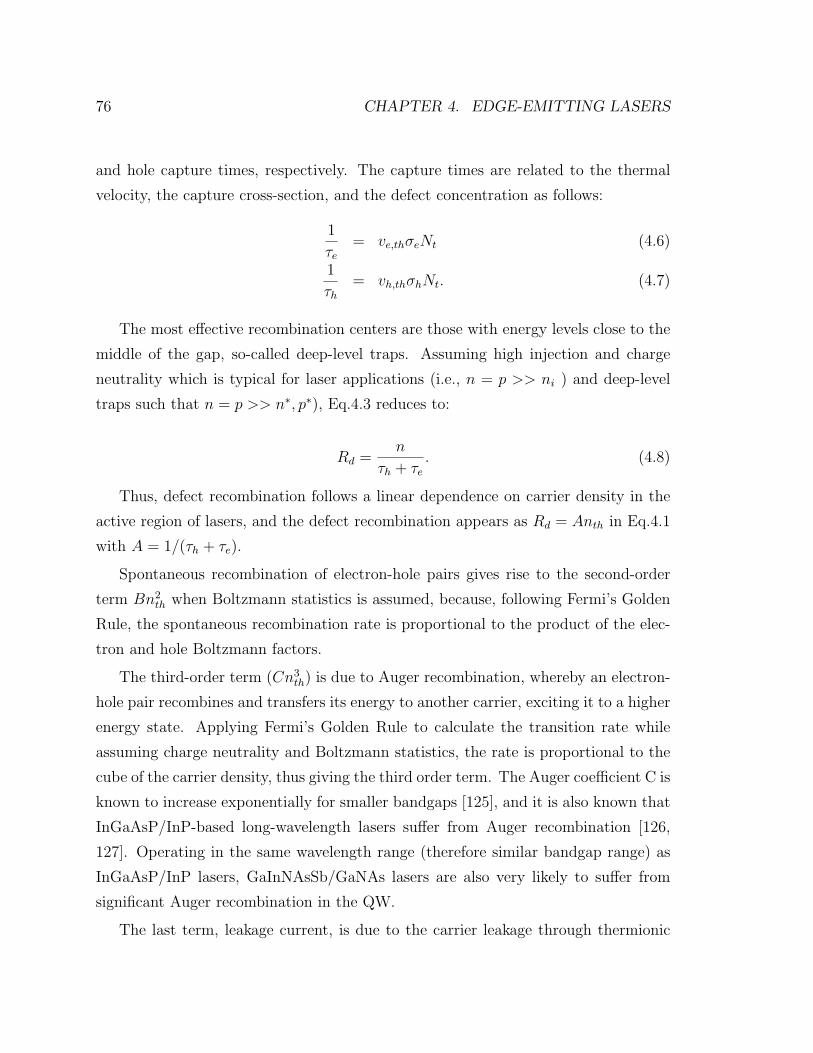
76 CHAPTER 4. EDGE-EMITTING LASERS
and hole capture times, respectively. The capture times are related to the thermal
velocity, the capture cross-section, and the defect concentration as follows:
1
τe
= ve,thσeNt (4.6)
1
τh
= vh,thσhNt. (4.7)
The most effective recombination centers are those with energy levels close to the
middle of the gap, so-called deep-level traps. Assuming high injection and charge
neutrality which is typical for laser applications (i.e., n = p >> ni ) and deep-level
traps such that n = p >> n∗, p∗), Eq.4.3 reduces to:
Rd =n
τh + τe
. (4.8)
Thus, defect recombination follows a linear dependence on carrier density in the
active region of lasers, and the defect recombination appears as Rd = Anth in Eq.4.1
with A = 1/(τh + τe).
Spontaneous recombination of electron-hole pairs gives rise to the second-order
term Bn2th when Boltzmann statistics is assumed, because, following Fermi’s Golden
Rule, the spontaneous recombination rate is proportional to the product of the elec-
tron and hole Boltzmann factors.
The third-order term (Cn3th) is due to Auger recombination, whereby an electron-
hole pair recombines and transfers its energy to another carrier, exciting it to a higher
energy state. Applying Fermi’s Golden Rule to calculate the transition rate while
assuming charge neutrality and Boltzmann statistics, the rate is proportional to the
cube of the carrier density, thus giving the third order term. The Auger coefficient C is
known to increase exponentially for smaller bandgaps [125], and it is also known that
InGaAsP/InP-based long-wavelength lasers suffer from Auger recombination [126,
127]. Operating in the same wavelength range (therefore similar bandgap range) as
InGaAsP/InP lasers, GaInNAsSb/GaNAs lasers are also very likely to suffer from
significant Auger recombination in the QW.
The last term, leakage current, is due to the carrier leakage through thermionic

4.3. RECOMBINATION MECHANISMS 77
emission over a heterostructure barrier of finite height. The rate of carrier leakage is
theoretically derived [128–130] to be:
Jleak =4πqk2T 2m
h3exp(−Eb − Ef
kT) (4.9)
This equation is straightforward, but it only gives an upper bound to the leakage
current for a semiconductor laser, because this equation was derived assuming that
carriers do not come back after going over the potential barrier, while in a semi-
conductor QW laser carriers may come back by diffusion or be recaptured before
being lost by diffusing away or recombining. Actual leakage current is typically only
20%–30% of the value suggested by Eq.4.9 [125] and more complete analysis requires
consideration of diffusion parameters [125]. However, despite this complication, the
exponential dependence on temperature would always be valid.
In our GaInNAsSb/GaNAs QW lasers, there are three areas (layers) to which
carriers can leak.
• AlGaAs cladding layers
• GaAs SCH region
• GaNAs barriers
For the Al.33Ga.67As cladding layers used for this study, the hetero-barrier between
the GaAs SCH layer and the doped AlGaAs cladding layer is as high as 400meV [131],
so leakage over to the AlGaAs claddings is expected to be very small ( < 1A/cm2
) [132].
The band offset between the GaAs SCH layer and the GaInNAsSb QW is∼500meV
for electrons and ∼160meV for heavy holes, as shown in Fig.4.6. This is larger than
or at least as large as the band offsets for InGaAs/GaAs lasers (Fig.4.7), for which
leakage to the GaAs SCH region is known to be not problematic [130]. Therefore,
it is fair to assume that leakage to the GaAs SCH region is not an issue for GaIn-
NAsSb/GaNAs lasers either.
The band offsets for the GaNAs/GaInNAsSb interface are however much lower,
with ∼160meV for electrons and <100meV for heavy holes. This can lead to a large

78 CHAPTER 4. EDGE-EMITTING LASERS
20 40 60
0.00
0.05
0.10
0.15
1.0
1.2
1.4
20 40 60 20 40 60
(a)
HH LH
E
nerg
y (e
V)
x = 2.2%y = 3.1%
x = 2.8%y = 3.8%
(b)
Distance (nm)
x = 3.0%y = 4.3%
(c)
Ga0.62In0.38NxAs0.991-xSb0.009/GaNyAs1-y/GaAs
Figure 4.6: Band offsets of GaInNAsSb/GaNAs QWs measured by contactless electro-reflectance. [133]
Figure 4.7: Band offsets of InGaAs/GaAs and InGaAsN/GaAs [6]

4.3. RECOMBINATION MECHANISMS 79
carrier population in the GaNAs barriers. This large population would not be a
problem if the quality of GaNAs material is high, with most of the carriers eventually
relaxing to lower QW energy levels from which they recombine radiatively to give
rise to spontaneous emission or optical gain. On the other hand, if the quality of the
GaNAs barriers is poor, the carriers in the barriers will recombine non-radiatively,
giving rise to a ’leakage current’. This leakage current would be very sensitive to
temperature, as the carrier population in the barrier has an exponential dependence
on temperature through the Boltzmann factor in Eq.4.9. It has been found, unfortu-
nately, that GaNAs layers are of relatively poor quality with a high concentration of
defects [73,92,97], so it is expected that leakage to the GaNAs barriers is a significant
component of threshold current [132]. From purely theoretical considerations, use of
GaAs barriers instead of GaNAs would be a natural solution to this problem, but in
practice GaNAs was introduced intentionally in order to overcome the material quality
problem by providing strain compensation to the highly strained GaInNAsSb/GaAs
QWs when emission wavelengths longer than 1.4µm are required [3, 23,28,79].
A closer look at the strain and bandgap of a GaInNAsSb/GaNAs QW (Fig.4.6)
reveals that the leakage problem is bigger than one might expect from the Boltzmann
factor alone, because the in-plane light hole mass in the GaNAs layer is a few times
larger than the in-plane heavy hole mass in the GaInNAsSb layer, due to the strain
effects [134]. Because the in-plane mass is proportional to the density of states, the
LH levels in the GaNAs barrier has a few times larger density of states compared to
the HH levels in the GaInNAsSb. Larger width of confinement for the holes in the
GaNAs barriers also increases the number of confined levels, further increasing the
number of available hole states in the GaNAs barrier. A simplified simulation of the
QW shows the severity of the situation, with the rapidly increasing density of states
above the barrier leading to significant hole population in the higher energy levels
(Fig.4.8).
Components of threshold current other than the spontaneous emission term rep-
resent unnecessary loss of carriers, increasing the threshold current and also degrad-
ing other performance metrics via increased junction temperature. For GaInNAsSb
QWs, we have been focusing on the defect recombination term for minimization of

80 CHAPTER 4. EDGE-EMITTING LASERS
−0.05 0 0.05 0.1 0.150
5
10
15x 10
35
Hole Energy above EV(eV)
Hole distribution at 300K, n=2*1012(cm−2)
HH1 HH2 LH1LH2
HH3LH3LH4
DOS
Fermi−Dirac factor
EV
Below barrier Above barrier
Figure 4.8: Hole distribution at 300K.
the threshold current, by measuring the PL intensity. However, other nonradiative
terms ( Auger and leakage ) have to be considered to achieve lower laser threshold as
dicussed above. Moreover, Auger and leakge terms also degrade another important
performance criteria, namely the temperature stability of lasers, so identification and
reduction of these terms is even more important. On the other hand, poor temper-
ature stability of a laser can be a sign of presence of Auger or leakage processes.
The relationship between the components in the laser threshold and the temperature
stability is discussed in the following sections.
4.4 Temperature stability : Theory
Temperature stability of laser threshold is a very important parameter for commercial
viabibility of semiconductor lasers, because poor temperature stability often leads to
requirements of additional temperature control or bias point control, driving the
system cost higher. Poor temperature stability of InGaAsP/InP lasers due to their
small conduction band offset and Auger recombination is one of the reasons of high
cost of semiconductor laser systems for optical communications. The promise of

4.4. TEMPERATURE STABILITY : THEORY 81
better temperature stability thanks to a higher conduction band offset was one of
the important motivations for pursuing dilute nitride research [17]. This promise
has been more or less realized for 1.3µm lasers [30–35, 37–39, 130], but it has not
been really realized for 1.5µm lasers. Before jumping into our experimental results
of temperature stability measurements, we first discuss the theory of temperature
stability of laser threshold.
Temperature stability of threshold current is usually expressed by using the char-
acteristic temperature T0, assuming the following exponential relationship [125]:
Ith = Ith0 exp(T
T0
). (4.10)
T0 can be calculated from measurements of threshold vs. temperature using the
following equation [127]:1
T0
=d[ln(Ith)]
dT(4.11)
The threshold current can be decomposed into a few components according to
Eq.4.1, and each component shows different characteristic temperature when it is
dominant, as discussed below. Eq.4.1 is repeated here for easy reference.
Ith = qV (Anth + Bn2th + Cn3
th + Rleak) (4.12)
The temperature dependence of the recombination coefficients A, B, and C is
expected to be [135,136]:
A ∝ T 1/2 (4.13)
B ∝ T−1 (4.14)
C ∝ exp(−Ea
kT) (4.15)
where Ea is the activation energy for the Auger process.
The threshold carrier density nth follows a slightly super-linear dependence on
temperature [127]:
nth ∝ T 1+x (4.16)

82 CHAPTER 4. EDGE-EMITTING LASERS
where x = 0 in an ideal QW in an ideal semiconductor laser. For real QWs for which
we have to consider occupation of higher subbands, carrier spillover, or temperature-
dependent IVBA, x becomes positive, making nth more sensitive to temperature.
If defect recombination (Anth) is dominant,
T0 =T
1.5 + x. (4.17)
If spontaneous recombination (Bn2th) is dominant,
T0 =T
1 + 2x. (4.18)
If Auger recombination (Cn3th) is dominant,
T0 =T
3 + 3x + Ea/kT(4.19)
where Ea is the activation energy for the Auger process. Ea is expected be 20–30meV
for phonon-assisted processes and ≤70meV for direct processes [127].
On the other hand, the leakage current is proportional to exp(−Ebarrier
kT), which
leads to
T0 = T ∗ kT
Ebarrier
. (4.20)
if leakage current is dominating the threshold current. ( Ebarrier is the effective height
of the energy barrier. ) T0 is thus larger for lower barriers and smaller for higher
barriers, although leakage current is less likely to be dominant for higher barriers. For
∼100meV barriers for holes in GaInNAsSb/GaNAs QWs, the leakage current could
actually dominate the threshold current density, driving T0 lower(∼ T/4).
In real semiconductor lasers, x is usually larger than 0, but smaller than 1 by
enough margin, so that T0 is relatively large when the threshold current is dominated
by defect recombination or spontaneous recombination, and T0 is smaller when the
threshold is dominated by Auger or leakage processes. For example, GaAs/AlGaAs
QW lasers and InGaAs/AlGaAs QW lasers show high T0 values ( 150–180K for
GaAs/AlGaAs lasers, and ≥200K for InGaAs/AlGaAs QW lasers [125] ) because

4.4. TEMPERATURE STABILITY : THEORY 83
they are dominated by the spontaneous recombination term. On the other hand,
InGaAsP/InP lasers in the 1.3–1.55µm range exhibit low T0 ( 50–70K ) due to Auger
recombination and leakage.
For 1.3µm GaInNAs/GaAs QW lasers, T0 values above 100K are routinely re-
ported, along with low threshold current density (250–320A/cm2) [30,31,35,39]. On
the other hand, GaInNAsSb/GaNAs QW lasers for ≥1.5µm have shown an interest-
ing tradeoff between low threshold current density and high temperature stability.
Our first generation 1.5µm laser had good temperature stability (T0=139K) but high
threshold current density (1.06kA/cm2) [51]. After improving the material quality
based on PL intensity measurements, the second generation of 1.5µm lasers showed
significantly improved threshold current density( 580A/cm2 ) but the temperature
stability degraded more significantly ( T0 = 73K ) [137]. This has been explained
by reduction of the defect recombination term by improving the QW material qual-
ity. Before the improvement, the threshold was dominated by defect recombination
leading to relatively high T0. If we reduce the defects in the QW, then Auger recom-
bination or leakage seem to dominate the threshold current, leading to much lower
T0.
It can be easily expected that 1.5µm GaInNAsSb/GaNAs lasers would experience
more Auger recombination ( due to smaller bandgap ) and more leakage current
( due to lower GaNAs barrier than GaAs ) than 1.3µm GaInNAsSb/GaAs lasers.
Therefore, lower T0 for 1.55µm lasers is not surprising. However, it has not been
really clear whether Auger recombination or leakage is more responsible for the lower
temperature stability, and this issue requires more research.
In order to gain more insight into which process is dominating the threshold
current density, temperature stability measurement results are presented for the latest
GaInNAsSb/GaNAs QW lasers in the next section. T0 is an important parameter for
its own right, too, as it is a measure of laser stability. A few different QW structures
were tried looking for the possibility of improving T0 without excessive increase in
the threshold current density. In addition, measurement results from a segmented
contact method [138, 139] are presented that gave us more clue about the origin of
non-radiative recombination in the GaInNAsSb/GaNAs QW lasers.

84 CHAPTER 4. EDGE-EMITTING LASERS
0 200 400 600 8000
10
20
30
40
50
60
Current(mA)
Pow
er(m
W)
T=15oC T=65oC
Figure 4.9: Pulsed L-I curve for a 2050µm×20µm laser.
4.5 Temperature stability measurements and Ori-
gin of nonradiative recombination
Temperature stability measurements for the same laser as in Fig.4.3 and Fig.4.4 are
shown in Fig.4.9 and Fig.4.10.
Similar to previous low threshold 1.5µm or 1.55µm lasers, this laser has a relatively
low T0 value, which implies that the threshold current is mainly dominated by Auger
or leakage processes. Low T0 also means that the threshold current has a steep
dependence on temperature. Fig.4.9 shows that the threshold nearly doubles as the
temperature changes from 15o to 65oC. In an effort to improve temperature stability,
we grew two more different QW structures as shown in Fig.4.11. In addition to the
standard single QW with 20nm GaNAs barriers that we have been discussing up to
this point, we also grew a 3QW laser and a SQW laser with thinner(10nm) GaNAs
barriers. With the 3QW lasers, we wanted to reduce the required gain per QW, thus
reducing nth and Auger recombination. With the thin-barrier lasers, we wanted to
reduce the amount of low-quality GaNAs material, in order to reduce the leakage
problem. We did not go all the way to removing GaNAs layers altogether, because
our previous attemps to use GaAs barriers resulted in very high laser threshold and
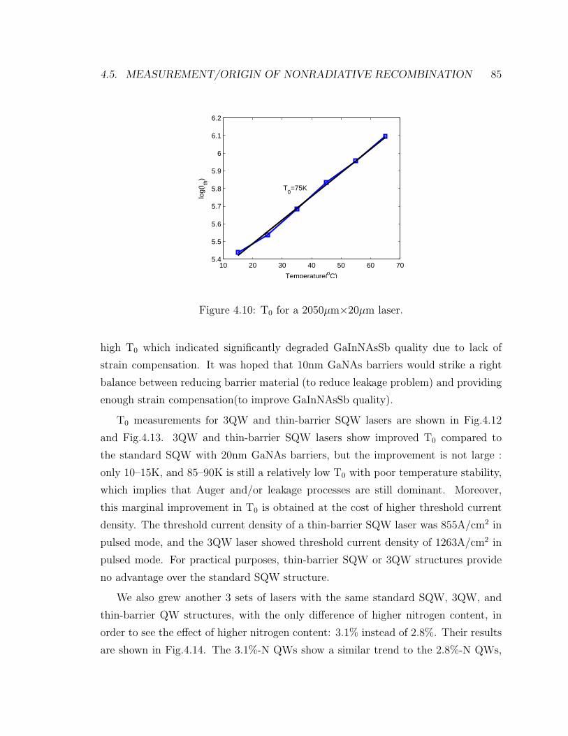
4.5. MEASUREMENT/ORIGIN OF NONRADIATIVE RECOMBINATION 85
10 20 30 40 50 60 705.4
5.5
5.6
5.7
5.8
5.9
6
6.1
6.2
Temperature(oC)
log(
I th)
T0=75K
Figure 4.10: T0 for a 2050µm×20µm laser.
high T0 which indicated significantly degraded GaInNAsSb quality due to lack of
strain compensation. It was hoped that 10nm GaNAs barriers would strike a right
balance between reducing barrier material (to reduce leakage problem) and providing
enough strain compensation(to improve GaInNAsSb quality).
T0 measurements for 3QW and thin-barrier SQW lasers are shown in Fig.4.12
and Fig.4.13. 3QW and thin-barrier SQW lasers show improved T0 compared to
the standard SQW with 20nm GaNAs barriers, but the improvement is not large :
only 10–15K, and 85–90K is still a relatively low T0 with poor temperature stability,
which implies that Auger and/or leakage processes are still dominant. Moreover,
this marginal improvement in T0 is obtained at the cost of higher threshold current
density. The threshold current density of a thin-barrier SQW laser was 855A/cm2 in
pulsed mode, and the 3QW laser showed threshold current density of 1263A/cm2 in
pulsed mode. For practical purposes, thin-barrier SQW or 3QW structures provide
no advantage over the standard SQW structure.
We also grew another 3 sets of lasers with the same standard SQW, 3QW, and
thin-barrier QW structures, with the only difference of higher nitrogen content, in
order to see the effect of higher nitrogen content: 3.1% instead of 2.8%. Their results
are shown in Fig.4.14. The 3.1%-N QWs show a similar trend to the 2.8%-N QWs,

86 CHAPTER 4. EDGE-EMITTING LASERS
• Single QW– 20nm GaNAs on both sides
• Thin-barrier QW– 10nm GaNAs on both sides
• Smaller number of energy levels in the barrier– GaAs barrier didn’t work due to strain
• 3QW– 20nm GaNAs between QWs
• Smaller nth per QW
GaNAs
GaInNAsSb
GaAsGaAs
Figure 4.11: 3 different QW structures
10 20 30 40 50 60 705.9
6
6.1
6.2
6.3
6.4
6.5
Temperature(oC)
log(
I th)
T0=89K
Figure 4.12: T0 for a thin-barrier laser, 2050µm×20µm.

4.5. MEASUREMENT/ORIGIN OF NONRADIATIVE RECOMBINATION 87
10 20 30 40 50 60 706.1
6.2
6.3
6.4
6.5
6.6
6.7
6.8
6.9
Temperature(oC)
log(
I th)
T0=85K
Figure 4.13: T0 for a 3QW laser, 2050µm×20µm.
with the 3QW and thin-barrier SQW lasers showing marginal (if at all) improvement
in T0 at the cost of a significant increase in the threshold. Higher nitrogen in the
QWs generally led to higher threshold and lower T0. This can be explained equally
well by increased Auger recombination due to a smaller bandgap, or by increased
leakage due to decreased light-hole barrier1.
Low T0 for all three QW structures indicate that highly temperature-sensitive
carrier loss mechanisms (i.e., Auger and leakage) are dominating the laser threshold.
This same conclusion that Auger and/or leakage is dominant has been obtained on
our previous generations of lasers [52,55,132], especially after improving QW quality
and laser threshold by reducing defects in the QW. Unfortunately, we have not been
able to clarify which one of the two mechanisms is dominating the laser performance.
This has to be determined in order to further reduce laser threshold and increase T0.
In order to identify the most dominant mechanism in the laser threshold, the laser
samples were characterized using segmented contact method by our collaborators at
Cardiff University, UK. Under this method, an edge-emitting laser bar is fabricated
1Due to limited number of effusion cells in the MBE growth chamber and the inverse proportion-ality of nitrogen incorporation with respect to the growth rate, we are forced to put more nitrogen inthe GaNAs layer as we increase nitrogen in the GaInNAsSb layer. With more nitrogen, the tensilestrain of the GaNAs layer increases.
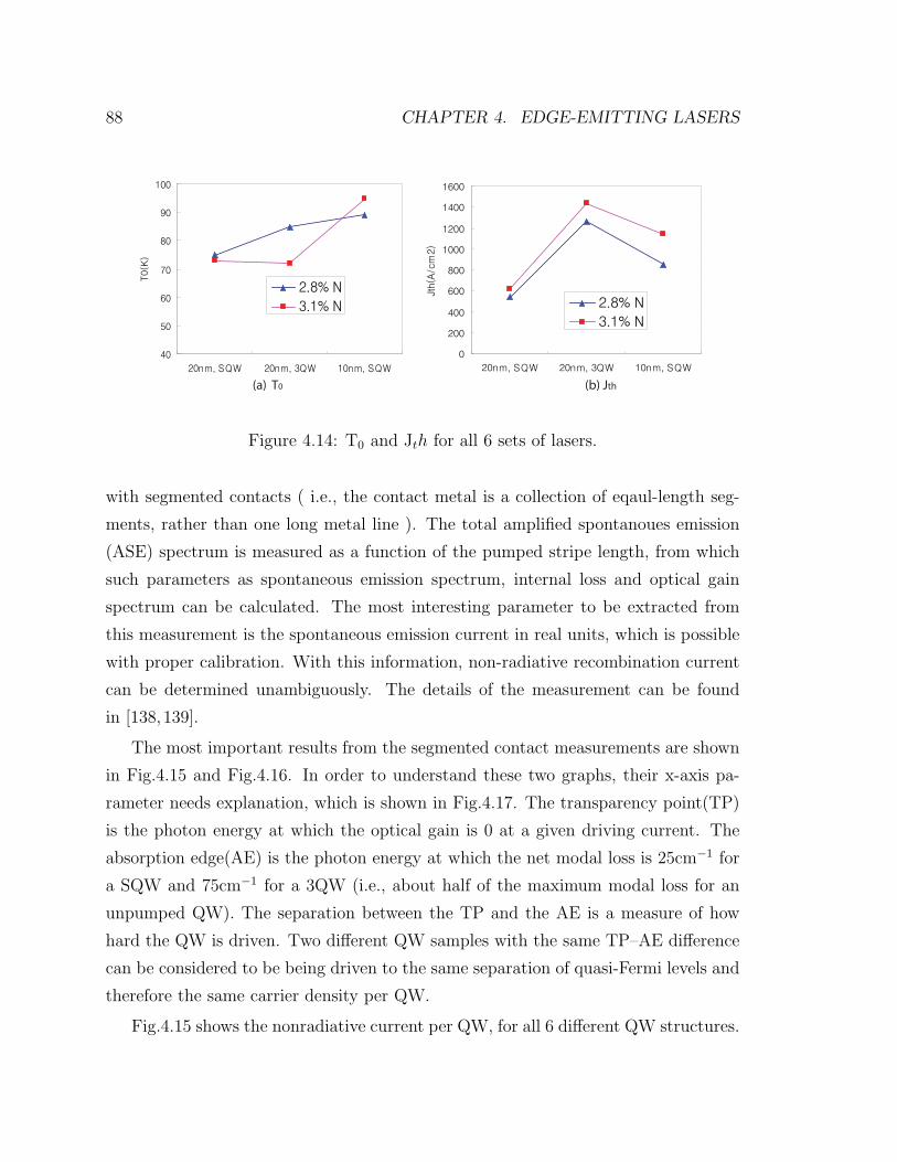
88 CHAPTER 4. EDGE-EMITTING LASERS
40
50
60
70
80
90
100
20nm, SQW 20nm, 3QW 10nm, SQW
T0(K
)
2.8% N
3.1% N
0
200
400
600
800
1000
1200
1400
1600
20nm, SQW 20nm, 3QW 10nm, SQW
Jth(A
/cm
2)
2.8% N
3.1% N
(a) T0 (b) Jth
Figure 4.14: T0 and Jth for all 6 sets of lasers.
with segmented contacts ( i.e., the contact metal is a collection of eqaul-length seg-
ments, rather than one long metal line ). The total amplified spontanoues emission
(ASE) spectrum is measured as a function of the pumped stripe length, from which
such parameters as spontaneous emission spectrum, internal loss and optical gain
spectrum can be calculated. The most interesting parameter to be extracted from
this measurement is the spontaneous emission current in real units, which is possible
with proper calibration. With this information, non-radiative recombination current
can be determined unambiguously. The details of the measurement can be found
in [138,139].
The most important results from the segmented contact measurements are shown
in Fig.4.15 and Fig.4.16. In order to understand these two graphs, their x-axis pa-
rameter needs explanation, which is shown in Fig.4.17. The transparency point(TP)
is the photon energy at which the optical gain is 0 at a given driving current. The
absorption edge(AE) is the photon energy at which the net modal loss is 25cm−1 for
a SQW and 75cm−1 for a 3QW (i.e., about half of the maximum modal loss for an
unpumped QW). The separation between the TP and the AE is a measure of how
hard the QW is driven. Two different QW samples with the same TP–AE difference
can be considered to be being driven to the same separation of quasi-Fermi levels and
therefore the same carrier density per QW.
Fig.4.15 shows the nonradiative current per QW, for all 6 different QW structures.

4.5. MEASUREMENT/ORIGIN OF NONRADIATIVE RECOMBINATION 89
Figure 4.15: Non-radiative current divided by the number of wells. Closed red symbols3.3%N, open blue symbols 3%N. Circles are thin barrier SQW, Triangles are thickbarrier SQW and squares are 3QW
Figure 4.16: Non radiative current divided by total barrier width. Closed red symbols3.3%N, open blue symbols 3%N. Circles are thin barrier SQW, Triangles are thickbarrier SQW and Squares are 3QW

90 CHAPTER 4. EDGE-EMITTING LASERS
-150
-100
-50
0
0.77 0.80 0.83 0.86
AE
TP
Energy / Ev
Net
Mod
al G
ain
/ cm
-1
Figure 4.17: Definition of the absorption edge and transparency point extracted fromthe modal gain and loss spectra
The standard SQW (with 20nm GaNAs barrier), thin-barrier SQW, and 3QW lasers
all have different nonradiative current per QW, which suggests that Auger recom-
bination or defect recombination is probably not the dominant mechanism, because
the non-radiative recombination current per QW would be independent of barrier
thickness or number of QWs if defect or Auger recombination were dominant.
On the other hand, Fig.4.16 shows nonradiative current per nm of GaNAs barrier
material. It is to be noted that the standard (thick-barrier) SQW, the thin-barrier
SQW, and the 3QW have a total of 40nm, 20nm, and 80nm of GaNAs barrier material,
respectively. In this figure, it is very interesting that the thick-barrier SQW and the
3QW lasers lie on the same line, indicating that for these two structures the non-
radiative recombination is the same for the same thickness of GaNAs material, which
in turn implies that the leakage into and non-radiative recombination in the GaNAs
barriers is the most dominant non-radiative carrier loss mechanism.
It is interesting to note that in both Fig. 4.15 and Fig. 4.16, the thin-barrier
SQW lies significantly higher in the graph, indicating disproportionately higher non-
radiative current. It is well known that 20-nm GaNAs barriers result in much better
QW quality than GaAs barriers due to strain compensation, and it is suspected that

4.5. MEASUREMENT/ORIGIN OF NONRADIATIVE RECOMBINATION 91
0
0.1
0.2
0.3
0.4
0 20 40 60 80 100Annealing minutes (680C)
PL
peak
inte
nsity
(A
.U.)
20nm GaNAs barrier10nm GaNAs barrierGaAs barrier
Figure 4.18: PL intensity of GaInNAsSb QW for 20nm, 10nm, and 0 GaNAs barrierthicknesses
10-nm GaNAs layers do not provide enough strain compensation, resulting in poorer
material quality (i.e., more defects) in the QW. This hypothesis is corraborated in
Fig.4.18, where PL intensity degrades as the thickness of GaNAs barriers is reduced.
Another interesting point is that the comparison between higher-nitrogen and
lower-nitrogen samples does not show much difference in Fig.4.15 and Fig.4.16, which
refutes the previously highly-held conception that more nitrogen leads to more de-
fects in the QW and degraded laser performance. In this experiment, non-radiatiave
recombination for a given TP–AE difference is the same, even for increased nitrogen
content, indicating the same QW quality. On the other hand, higher-nitrogen QWs
are found to have higher internal loss (12 vs. 6 cm−1 for thin-barrier SQW, and 18
vs. 14 cm−1 for 3QW [140]), leading to higher threshold current.
Now that leakage current appears to be the dominant carrier loss mechanism in
the active layer of the GaInNAsSb/GaNAs QW lasers, further improvement of laser
performance, including both T0 and Jth, should come from a reduction of this carrier
leakage component. As this leakage current results from the combination of low band
offset and poor barrier material quality, it can be tackled by either improving the
barrier material quality or increasing the band offset.

92 CHAPTER 4. EDGE-EMITTING LASERS
The quality of GaNAs barrier material was investigated by PL measurements of
GaNAs/GaAs QWs [92] and was found to be rather insensitive to growth conditions.
It is thus not clear whether the GaNAs quality has the potential for significant im-
provement. On the other hand, the addition of small amount of Sb to the GaNAs
layer was found to improve the quality significantly, while addition of large amount of
Sb degraded the material quality [92, 141]. This observation can be used to improve
the barrier material quality by using GaNAsSb layer with the proper Sb composition.
Unfortunately, in our system with a non-valved Sb cracker, it is not possible to change
the Sb flux fast enough between the GaNAsSb barrier and the GaInNAsSb QW to
adequately control the Sb composition. Thus, our growth process incorporates too
much Sb in the GaNAsSb layer when the proper amount of Sb is incorporated in the
GaInNAsSb QW. A valved Sb cracker or an additional Ga cell needs to be installed
on the MBE chamber in order to obtain higher quality GaNAsSb barriers.
Increasing the barrier height appears to be a more feasible solution with the cur-
rent configuration of our MBE chamber, as a phosphorous cell is already installed,
which enables growth of GaAsP layers. GaAsP is tensily strained on GaAs and has
a higher bandgap than GaAs, so it satisfies both requirements of high barrier height
and strain compensation at the same time. This is a very promising opportunity
for improving GaInNAsSb lasers, but growth of GaAsP barrier layers also has its
challenges, especially with the unvalved GaP source we currently have. A significant
amount of phosphorous goes around the shutter even when it is closed, so a signif-
icant amount of phosphorous incorporates into the GaInNAsSb layer, increasing its
bandgap and possibly affecting its quality. The larger bandgap of GaAsP can also
affect the carrier capture efficiency into the QW. This will affect the PL samples and
lasers, reducing the observed PL intensity and/or the modulation speed of lasers.
Despite these challenges, growth of high quality GaInNAsSb/GaAsP QWs is being
attempted at the time of writing, which, if successful, can help realize low-threshold
and high-T0 lasers at 1.55µm on GaAs substrates.

4.5. MEASUREMENT/ORIGIN OF NONRADIATIVE RECOMBINATION 93
High QualityGaNAs:Sb Barriers
Suppress thermionic emission
XGaAs GaAsX
GaAs
GaAs(P) Barriers
(a) Higher quality barrier (b) Higher band o�set
Figure 4.19: Two approaches to reduce leakage problem.

Chapter 5
1528nm VCSEL
Realization of vertical-cavity surface-emitting lasers (VCSELs) for communications
wavelengths of 1.3–1.6µm has been a very important motivation for the substantial
research efforts for GaInNAs(Sb) material. The advantages of VCSELs compared
to edge-emitting lasers include lower threshold current, better coupling with optical
fibers, better temperature stability of emission wavelength, much easier testing, and
the possibility of making 1-D or 2-D arrays for high-density interconnects.
However, VCSELs have not been available for some important wavelengths, es-
pecially the wavelengths approrite for fiber communications. Like conventional edge-
emitting lasers, VCSELs are composed of an active region and a pair of mirrors around
the active region. Unlike the edge emitting lasers for which simple cleaved facets with
or without dielectric coating are sufficient as the mirrors, much more complex dis-
tributed Bragg reflectors (DBRs) are necessary for the mirrors for a VCSEL. These
are necessary because of the requirement to achieve very high reflectivity over 99%,
and a vertical configuration for the cavity. DBRs require high quality deposition of
many alternating layers of different refractive indices and GaAs provides the best sub-
strate for making such DBRs, thanks to the availability of the AlGaAs alloy system
which provides good index contrast, good electrical/thermal conductivities, and close
lattice match to GaAs.
The challenge has been that emission in 1.3–1.6µm wavelength range was not
available from III-V alloys lattice-matched to GaAs substrates, until the discovery
94

95
of GaInNAs(Sb) [15, 17]. On the other hand, InGaAsP, which is lattice-matched to
InP substrates, is able to emit in the 1.3–1.6µm wavelength range, but it has lacked
a simple, reliable, and commercially viable DBR material technology despite many
efforts and some laboratory successes [142,143].
GaInNAsSb material enables VCSELs in the communications wavelength range
by providing the long-awaited optical gain. VCSELs around 1.3µm wavelength were
realized [67,144] using GaInNAs QWs not long after the first reports of dilute nitrides
[15,16]. Since then, low threshold current (1–2mA), low threshold voltage (<2V), high
output power(0.8mW or higher) [44–46], and 10Gbps direct modulation [47,145,146]
have been reported.
On the other hand, GaInNAs(Sb) VCSELs over 1.5µm wavelength have been very
slow to be realized. The biggest hurdle has been the difficulty of achieving high-quality
QWs for longer wavelengths, as more indium and nitrogen must be incorporated. This
problem was greatly alleviated by the addition of antimony [91,147], but it still took
significant time and effort to improve the QW quality and achieve low-threshold edge-
emitting lasers [96, 122, 148], the first VCSELs at 1.46µm VCSEL [53] and then at
1.53µm [54]. Despite significant efforts, these VCSELs have not achieved continous
wave(CW) operation at room temperature.
In addition to the QW quality problem, low loss DBRs also posed significant chal-
lenges for 1.5µm or longer-wavelength VCSELs, because the index contrast between
GaAs and AlGaAs layers is smaller and the free carrier absorption is larger for longer
wavelengths. There also have been practical issues with our MBE system, such as the
difficulty of thickness control due to flux fluctuation from the effusion cells and the
random quality problems either due to the ”mystery” pressure burps in the chamber
and the instabiilty of the plasma cell.
We were able to achieve CW operation near room-temperature and pulsed op-
eration at room temperature for a 1528nm GaInNAsSb VCSEL by combining im-
provmenets in the MBE chamber, growth and annealing conditions that have been
researched over many generations of graduate students and careful design and con-
trol of the thicknesses and doping of the epitaxial layers. The current VCSEL design,
growth, fabrication, and results are described in the following sections.

96 CHAPTER 5. 1528NM VCSEL
5.1 Structure and design
The gain and loss in a VCSEL should satisfy the following equation for lasing to
occur [149]:
Γzgth = Γzαac + (1− Γz)αSCH +1
2Lln
1
R1R2
(5.1)
where L is the length of the cavity, Γz is the longitudinal (i.e., vertical for a
VCSEL) confinment factor, and αac and αSCH are internal losses from the active
region and the SCH region, respectively. According to [149], Γz = Γrd/L, where
d is the thickness of the active layer and Γr is a relative confinement factor, which
asymptotes to 2 when d is much smaller than L. Assuming Γr = 2 for simplicity as
we are dealing with QW active layers, the equation can be rewritten by multiplying
both sides by 2L to get an equation of gain and loss per round trip.
4dgth = 4dαac + 2(L− 2d)αSCH + ln1
R1R2
(5.2)
Assuming very high reflectivities for both mirrors, ln (1/R) can be approximated
by (1-R), so we have
4dgth = 4dαac + 2(L− 2d)αSCH + (1−R1) + (1−R2) (5.3)
The material gain at threshold gth follows the equation
gth = g0ln(ηJ
Jtr
) (5.4)
with g0 around 1000 per cm and Jtr/η around 600A/cm2 measured by the segmented
contact method [140] for the standard SQW lasers described in the previous chapter.
Using this data and assuming a linear increase in gain and current density with
increased number of QWs, the round-trip gain (4dgth) is calculated and shown in
Fig.5.1.
A SQW would be the best choice if we can guarantee very low round-trip loss, but
more QWs would be a safer choice considering the challenges facing the design and

5.1. STRUCTURE AND DESIGN 97
0 2 4 6 8 10 12 14 16 18 200
0.005
0.01
0.015
0.02
0.025
Current density(A/cm2)
Rou
nd−
trip
gai
n
SQW
2QW
3QW
4QW
Figure 5.1: Round-trip gain for different number of QWs
growth of the DBR mirrors. On the other hand, too many QWs can be challenging to
grow and may also break the assumption of Γr = 2 as the total active region thickness
increases. We chose 3 QWs as a trade-off.
An upper-bound for αac can be found from the measurements of SQW edge-
emitting lasers, where αi is found to be around 5cm−1 [140]. This αi contains losses
from both the active layer and the cladding, but if we assume all the loss is from the
active layer with confinement factor of 1.4% [55], αac can be estimated at 360cm−1
and 4dαac is about 0.003, or 0.3%.
αSCH can be assumed neglible as the SCH layer is undoped and the carrier den-
sity there would be quite small, even under strong forward bias thanks to the large
bandgap offset of GaAs from the GaInNAsSb QW.
Although not explicitly shown in the equations above, there is also diffraction (or,
scattering) loss due to the dielectric aperture when the aperture is defined by air or
oxide, or due to lack of index guiding when the aperture is defined by proton implant.
We chose to use oxide apertures defined by wet-oxidation of high-Al AlGaAs layer
[150,151], as it has the advantage of providing both optical and electrical confinement
at the same time.An analytical model for scattering loss due to dielectric apertures
is provided in [152], according to which we get an effective cavity length Lc = 2µm
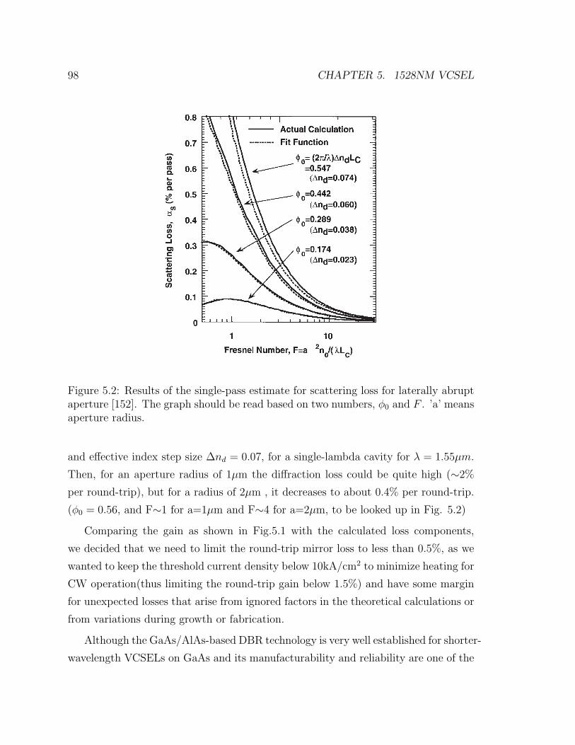
98 CHAPTER 5. 1528NM VCSEL
Figure 5.2: Results of the single-pass estimate for scattering loss for laterally abruptaperture [152]. The graph should be read based on two numbers, φ0 and F . ’a’ meansaperture radius.
and effective index step size ∆nd = 0.07, for a single-lambda cavity for λ = 1.55µm.
Then, for an aperture radius of 1µm the diffraction loss could be quite high (∼2%
per round-trip), but for a radius of 2µm , it decreases to about 0.4% per round-trip.
(φ0 = 0.56, and F∼1 for a=1µm and F∼4 for a=2µm, to be looked up in Fig. 5.2)
Comparing the gain as shown in Fig.5.1 with the calculated loss components,
we decided that we need to limit the round-trip mirror loss to less than 0.5%, as we
wanted to keep the threshold current density below 10kA/cm2 to minimize heating for
CW operation(thus limiting the round-trip gain below 1.5%) and have some margin
for unexpected losses that arise from ignored factors in the theoretical calculations or
from variations during growth or fabrication.
Although the GaAs/AlAs-based DBR technology is very well established for shorter-
wavelength VCSELs on GaAs and its manufacturability and reliability are one of the

5.1. STRUCTURE AND DESIGN 99
key motivations for GaInNAs(Sb) VCSEL research for 1.3 or 1.55µm wavelength
range, different optical properties of the DBR materials present additional challenges
for long wavelength VCSELs. The contrast between the two materials becomes
smaller for longer wavelengths, necessitating more mirror pairs to provide a given
reflectivity. Another serious challenge is that the free carrier absorption and inter-
valence-band absorption (IVBA) increase for longer wavelength, increasing mirror
loss, especially for the p-doped DBR mirror 1. Lower doping has to be used to limit
the optical loss, but then the elctrical resistance increases (again, more severe for the
p-doped mirror due to lower mobility), which leads to unnecessary device heating
and degradation of laser performance. Longer wavelength also means that each mir-
ror pair has to be thicker, which exacerbates all these optical, electrical and thermal
problems. These problems have indeed made the realization of 1550nm VCSELs quite
challenging, especially when combined with the growth challenges for GaInNAs(Sb)
QWs for 1.55µm emission.
It is possible to circumvent the challenges for DBR design at 1.55µm by using
alternative structures, such as intra-cavity contacts or a tunnel-junction, instead of
the simplest structure with one n-DBR and one p-DBR illustrated in Fig. 5.3 as a
conventional ’PIN’ structure. The intra-cavity contact structure uses undoped lay-
ers for one or both of the DBR mirrors and currents are injected through highly-
doped injection layers with electrical contacts placed between the active layer and
the DBR(s) [47, 48, 145, 146, 154]. The design of DBR mirrors becomes significantly
simpler, especially for the p-DBR, but it requires additional care and optimizations
for the best tradeoff between uniform current injection vs. lower optical loss. A
tunnel junction provides a conversion between n-type and p-type carriers with low
additional resistance, allowing us to use two n-DBRs instead of one n-DBR and one
p-DBR [42, 43, 155]. Without a high-optical-loss high-resistance p-DBR, it becomes
much easier to design the DBR mirrors. But this structure also requires significant
efforts to achieve high-quality growth with high doping confined to the thin tunnel
1According to the experimental results in [153], the absorption coefficient for 1018cm−3 p-typeGaAs is 13cm−1 at 1.3µm and 26cm−1 at 1.6µm. Very similar numbers are observed for InP andIn.4Ga.6As [153]. On the other hand, the absorption coeffiecient is about 5cm−1 for n-type GaAs at1.55µm.
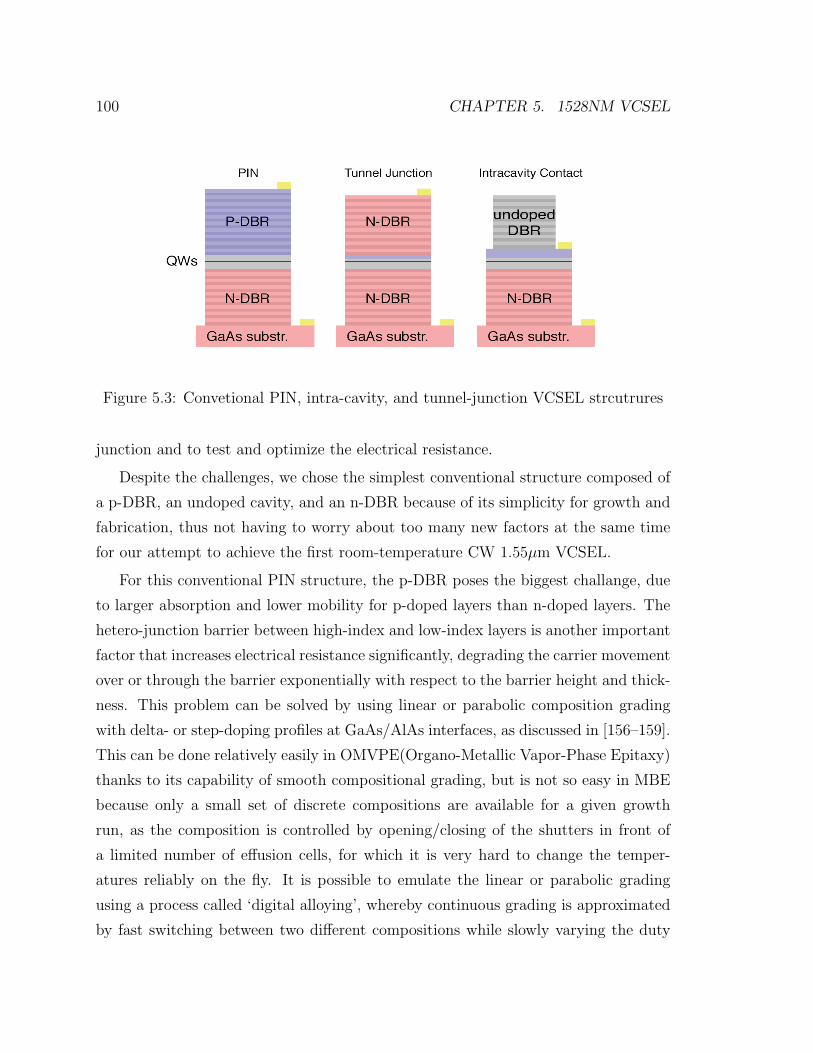
100 CHAPTER 5. 1528NM VCSEL
Figure 5.3: Convetional PIN, intra-cavity, and tunnel-junction VCSEL strcutrures
junction and to test and optimize the electrical resistance.
Despite the challenges, we chose the simplest conventional structure composed of
a p-DBR, an undoped cavity, and an n-DBR because of its simplicity for growth and
fabrication, thus not having to worry about too many new factors at the same time
for our attempt to achieve the first room-temperature CW 1.55µm VCSEL.
For this conventional PIN structure, the p-DBR poses the biggest challange, due
to larger absorption and lower mobility for p-doped layers than n-doped layers. The
hetero-junction barrier between high-index and low-index layers is another important
factor that increases electrical resistance significantly, degrading the carrier movement
over or through the barrier exponentially with respect to the barrier height and thick-
ness. This problem can be solved by using linear or parabolic composition grading
with delta- or step-doping profiles at GaAs/AlAs interfaces, as discussed in [156–159].
This can be done relatively easily in OMVPE(Organo-Metallic Vapor-Phase Epitaxy)
thanks to its capability of smooth compositional grading, but is not so easy in MBE
because only a small set of discrete compositions are available for a given growth
run, as the composition is controlled by opening/closing of the shutters in front of
a limited number of effusion cells, for which it is very hard to change the temper-
atures reliably on the fly. It is possible to emulate the linear or parabolic grading
using a process called ‘digital alloying’, whereby continuous grading is approximated
by fast switching between two different compositions while slowly varying the duty
5.1. STRUCTURE AND DESIGN 101
cycle. But this process requires a very large number of shutter operations, requiring
hundreds or even over thousand shutter operations per DBR growth, which presents
a significant reliability issue for the MBE machine. Especially problematic are the Ga
shutters, which can get stuck to the chamber wall because of wetting by the Ga melt
on them and then be bent out of shape when the shutter actuator tries to open/close
it forcefully. Use of externally-adjustable shutters greatly reduced the repair time
and the associated pain and risks of this shutter problem, but such a shutter problem
during a VCSEL growth is still very costly to recover from, setting us back by a few
days at best and a month or more in the worst case.
Therefore, we instead used step-wise composition grading for DBR interfaces to
limit the number of shutter operations, while still trying to minimize the electrical
resistance with minimum doping. The high-index layer is GaAs and the low-index
layer is 91% AlGaAs. There are 2 Ga cells and 2 Al cells in our System4 MBE chamber
used for DBR growth. To obtain the finest step-grading with minimum number of
shutter operations, we set the growth rates of Al1, Al2, Ga1, and Ga2 cells at 0.47,
0.23, 0.64, and 0.07 µm/hr respectively, and by following the sequence shown in Table
5.1, we get a 6-step grading in composition going from a GaAs to an Al.91Ga.09As
layer, over 30nm. Doping is higher in the graded interface (especially at the optical
nodes) than in the GaAs or Al.91Ga.09As layers, because the thermionic injection and
tunneling processes occuring in the graded interfaces have a much steeper dependence
on doping than the drift process occuring in a GaAs or Al.91Ga.09As layer. The base
doping level for the 91% AlGaAs layers was slowly increased from 3 ∗ 1017cm−3 for
the innermost layers (i.e., closest to the cavity) to 2 ∗ 1018cm−3 for the outermost
layers. Be was used to provide the slowly-varying low background p-doping for all
the layers, while C was added to increase doping in the graded regions2. On the other
hand, much steeper 3-step grading over 5nm is chosen for the n-DBR ( using only
layer #0, 1, 4, and 6 from Table 5.1 ), as the resistance problem is much less severe
for the n-DBR due to the higher mobility and the smaller effective mass for electrons
than holes.
2The Be effusion cell is harder to control quickly than the CBr4 source, and Be diffuses morereadily than C at high concentrations and while the wafer is heated up, i.e., during growth orannealing.

102 CHAPTER 5. 1528NM VCSEL
Layer index Al1 Al2 Ga1 Ga2 Al composition(x in AlxGa1−xAs)0 c c o o 01 c o o o 0.252 o c o o 0.403 o o o o 0.504 c o c o 0.775 o c c o 0.876 o o c o 0.91
Table 5.1: Shutter operations (o/c for open/closed) and composition grading. Specialcare was taken to reduce number of shutter operations, especially for the Ga shutters,which are more vulnerable.
We calculated the reflection, absorption, and transmission of the DBR mirrors
using a multi-layer 1-D transmission matrix solver, while changing the number of
layers until a proper level of reflectivity is attained. We first considered growing on a
p-type substrate, thus placing the p-DBR at the bottom and the n-DBR at the top
to help minimize the resistance of the p-DBR(the bottom DBR has a wider effective
area, as the top DBR is etched down to form a cylindrical mesa, while the bottom
DBR is not etched). But it was not possible to achieve less than 0.4% mirror loss (=
absorption + transmission ) for the p-DBR due to the wide 30-nm grading and the
high IVBA, without reducing the doping level too much. Since there must be some
transmission loss in the upper DBR to guarantee that the external efficiency does not
suffer too much, we suspected that the total mirror loss might be too high with this
structure. On the other hand, if we grow on an n-substrate, the bottom n-DBR can
attain reflectivity over 99.97% (due to narrower grading region and lower absorption
loss) and the upper p-DBR can attain 99.6% reflectivity. The bottom n-DBR has 35
layers, and the top p-DBR has 23 layers in our current design.
The first (closest to the cavity) Al.91Ga.09As layer in the p-DBR also serves as
the oxide aperture. The uppermost 40nm of this layer is Al.98Ga.02As, obtained
by alternating Al.91Ga.09As and AlAs layers 10 times (digital alloying). Because
the oxidation rate is exponentially faster for higher Al content [160], the thin 98%
AlGaAs layer oxidizes laterally first, and then the 92% AlGaAs layer oxidizes slowly

5.2. GROWTH AND FABRICATION 103
Chamber Name SourcesSystem4 Al1 Al2 Ga1 Ga2 As C Be SiSystem5 Ga In N P As Sb Be Si
Table 5.2: Current cell configurations for the two MBE chambers used for this thesiswork
downward. This results in a tapered profile of the oxide, with the aperture being the
narrowest at the optical node [161], which helps to minimize the scaterring loss.
5.2 Growth and fabrication
The VCSELs were grown in 3 steps in the two coupled MBE chambers. First, the
bottom n-DBR is grown in System4, which is the DBR machine with 2 Al and 2
Ga cells, and Si(n-type), Be(p-type) and CBr4(p-type) cells for doping. Second, the
cavity, including 3QW, is grown in System5, which is the nitride machine with the
N rf plasma cell. Finally, the top p-DBR is grown in System4. The current cell
configurations for the two MBE chambers are shown in Table 5.2. Note that each
chamber can have only up to 8 cells.
An apparently mundane, but very important challenge for the growth of VCSELs
is the control of growth thickness. Just 1% error in the growth thickness of the DBRs
or the cavity results in cavity/mirror wavelength error of 15nm, which can cause
significant mismatch with the gain spectrum of the GaInNAsSb QWs, resulting in
higher threshold or no lasing at all. To assure correct thicknesses, several growth
calibrations were made immediately before VCSEL growth, with the sources at their
final temperatures. The source temperatures are determined to get the desired growth
rate, based on the previous calibration growths and the fluxes measured with the ion
gauge. For each of the aluminum sources in System4, a 1000nm AlAs layer was grown
on GaAs for calibration. Normal-incidence, white-light reflectivity spectrum of the
wafer was taken and matched to simulation using the thin-film solver(mff), to get
the actual AlAs growth thickness. Another 1000nm of GaAs is grown on top of the
AlAs layer, and reflectivity measurements and simulations are repeated to calibrate

104 CHAPTER 5. 1528NM VCSEL
the GaAs growth rate.
Despite the growth rate calibration, the cells were found to be drifting with time.
This growth rate fluctuation was more common when older trumpet-shaped crucibles
were used, compared to newer SUMO cells from Veeco, which have a constriction at
the neck that better isolates the cell from the surrounding MBE chamber. They also
have a dual-zone heating system, with one heater at the tip and the other at the base
of the crucible. The gallium cell stability was greatly improved by keeping the tip
150-180oC hotter than the base [56], and this improved stability was a critical factor
in realizing previous 1.5µm-range GaInNAsSb VCSELs [53, 54]. On the other hand,
the 150-180oC temperature offset resulted in too many oval defects on the wafer3, so
we chose larger difference (210-240oC) for the growth of the VCSELs in this thesis.
This reduced the oval defect density, but degraded the cell stability.
Moreover, the dual-zone heating can not be applied to the aluminum cells, because
aluminum has an unfortunate property of creeping up the crucible wall ( made of
PBN, or pyrolytic boron nitride ) and overflowing, which can short out the heater
filament and destory the cell permanently. The aluminum cells therefore are heated
by a single heater at the base only. We found the flux instability of the aluminum
cells quite significant, changing as much as 5% after a bottom DBR growth, which
took as long as 14 hours. Because of the long growth time and the larger tip-base
temperature difference, the stability of the gallium cells was not strikingly better than
the aluminum cells, routinely showing 1–2% variation after each growth.
If two growths are done back-to-back without any adjustment in between, the
cell may deviate in the opposite direction during the second growth cancelling out
the deviation during the first growth, but it may also continue drifting in the same
direction, resulting in 2–4% total deviation. The flux deviation after each growth
tends to be one-way (i.e., downward) when there is little material left in the cell, but
the deviation was more random when there is enough material in the cell, probably
as the surface area of the melt sprawls and shrinks randomly over time. For other
growths such as edge-emitting lasers, a few percent of flux variation is not so critical,
3Gallium condenses on the tip if the tip is not hot enough. When the condensed droplets fall intothe gallium melt, small gallium droplets are spit onto the wafer [162]. Larger temperature differencebetween the tip and the base reduces the condensation and the oval defects.
5.2. GROWTH AND FABRICATION 105
but it is extremely critical for VCSELs. we thus chose to re-measure the growth rates
of the cells before the growth of each region(i.e., bottom DBR, active region, and top
DBR), so that we can adjust the cell temperatures in order to start the next growth
with correct fluxes. However, we did not go as far as repeating ’calibration growths’
between DBR growths, because one calibration run takes too long (2 days). Instead,
we depended on the fluxes measured by the ion gague to estimate the actual growth
rate at the moment, which turned out to be very accurate within 0.5%4.
Despite these efforts, the reflectivity spectrum of the DBRs and the cavity reso-
nance wavelength showed some deviation (up to 1%) from design, because we were
not able to monitor and control the growth rate on the fly5. To compensate for these
deviations, we grew the GaAs SCH region above the active region intentionally thin-
ner by 15nm than designed, so that compensation is possible even when the cavity is
thicker than designed and some thickness has to be removed from upper layers. Af-
ter cavity growth in System5 and before p-DBR growth in System4, the reflectivity
spectrum is measured, and compared with simulation. Because the air/GaAs inter-
face provides enough reflectivity, the cavity resonance can be easily observed. When
there is any deviation between the measured cavity resonance and the expected reso-
nance, the error in the thickness of the cavity can be estimated and compensated for
by adding/removing an approriate thickness from the first GaAs part of the upper
p-DBR growth.
To further ensure against any unexpected problems during growth, including wave-
length errors, we grew two VCSELs with two different resonance wavelengths, 1540nm
and 1560nm. Each of them showed 15-25nm wavelength error (shorter than designed)
right after the bottom DBR growth, so we decided to revise their resonance wave-
lengths to 1525nm and 1550nm, respectively, to ensure the bottom DBR reflectivity
spectrum is not too far off from the resonance. After cavity and upper DBR growths
using the corrections described above, each showed a cavity resonance at 1532nm and
4The reflectivity measurement and simulation used for the calibration growth can not providebetter than 0.5% accuracy, either.
5We considered using RHEED oscillations or reflectivity measurement for in-situ growth ratemonitoring, but both methods suffer too much from wafer wobble, the same problem that plaguedthe emissivity-compensated pyrometry (See Section 3.1.2).

106 CHAPTER 5. 1528NM VCSEL
1553nm, respectiviely, at the center of wafer. This is up to 0.5% deviation either from
the original wavelength targets or from the revised targets.
One unfortunate problem that occurred during growth was that the CBr4 source
that provides the carbon doping for the p-DBR did not control the CBr4 properly,
doping the inner-most DBR layers at several 1018cm−3’s, which was 5-10 times higher
than intended. We did not notice this problem until we had already grown a few
p-DBR layers for the second VCSEL, which was too late to correct the problem.
Without this problem, we expect the VCSELs would have shown better performance,
such as lower threshold or higher output power, than reported here.
After growth of the VCSELs, they were annealed in an RTA for 7 minutes at
670oC, which was determined by finding the optimal annealing condition for a PL
sample that was grown on the same day and treated with the same self-annealing in
the MBE chamber as the VCSEL wafers. Ring-shaped Ti/Pt/Au contacts were first
defined by lift-off method. Cylinder-shaped mesas ranging in diameter from 18 to
36µm were defined by lithography and DRIE etching down to the top of the bottom
DBR. Wet oxidation of the oxide aperture was carried out in the GaAs oxidation
furnace filled with N2 gas saturated with water. Fabrication is completed with the
deposition of Au/Ge/Ni/Au contact layer on the wafer backside, and the wafer is
annealed at 420oC for 1 minute for Au/Ge/Ni/Au contact alloying.
5.3 Measurements
The VCSELs were mounted epi-side up on a copper chuck for testing. Below the
copper chuck was a thermoelectric cooler (TEC), feedback-controlled to maintain a
constant temperature. The n-side electrical connection is made through the copper
chuck and the bottom n-contact of the VCSEL wafer, and the p-side electrical con-
nection is made by placing a probe tip on top of a top ring contact. Optical output
power is measured using an integrating sphere and a Thorlabs PDA400 amplified
photodetector, and the emission spectrum is measured by coupling the light output
into a 62.5µm multimode fiber through collimating lenses. The whole measurement
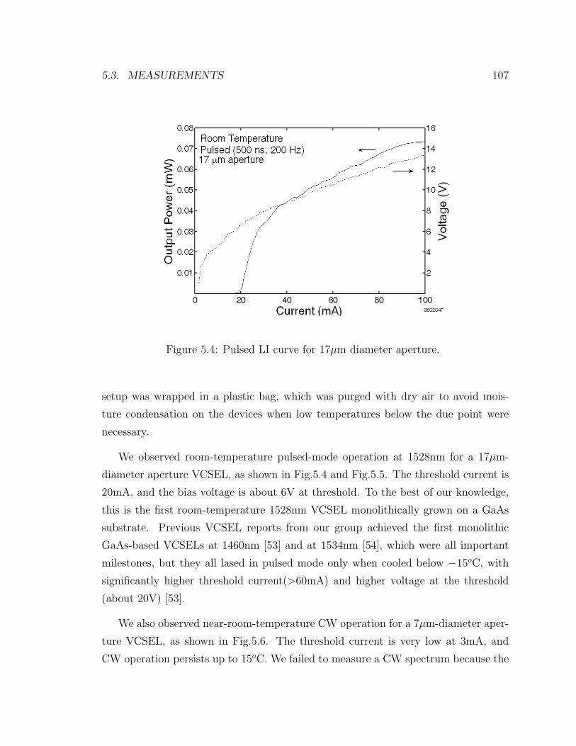
5.3. MEASUREMENTS 107
Figure 5.4: Pulsed LI curve for 17µm diameter aperture.
setup was wrapped in a plastic bag, which was purged with dry air to avoid mois-
ture condensation on the devices when low temperatures below the due point were
necessary.
We observed room-temperature pulsed-mode operation at 1528nm for a 17µm-
diameter aperture VCSEL, as shown in Fig.5.4 and Fig.5.5. The threshold current is
20mA, and the bias voltage is about 6V at threshold. To the best of our knowledge,
this is the first room-temperature 1528nm VCSEL monolithically grown on a GaAs
substrate. Previous VCSEL reports from our group achieved the first monolithic
GaAs-based VCSELs at 1460nm [53] and at 1534nm [54], which were all important
milestones, but they all lased in pulsed mode only when cooled below −15oC, with
significantly higher threshold current(>60mA) and higher voltage at the threshold
(about 20V) [53].
We also observed near-room-temperature CW operation for a 7µm-diameter aper-
ture VCSEL, as shown in Fig.5.6. The threshold current is very low at 3mA, and
CW operation persists up to 15oC. We failed to measure a CW spectrum because the

108 CHAPTER 5. 1528NM VCSEL
Figure 5.5: Spectrum of a pulsed 1528nm VCSEL at 1.2× threshold.
15 C
-5 C
5 C
o
o
o
Figure 5.6: CW LI curve of a 7 µm-aperture VCSEL

5.3. MEASUREMENTS 109
probe tip was very unstable on the small top contact, slipping away at a small vibra-
tion of the testing setup. For future generations of VCSELs, it would be beneficial to
apply planarization and provide a larger probe-landing area for the top contact, for
easier testing as well as better heat-sinking.
This is the first-ever CW VCSEL on GaAs to the best of our knowledge, which is
a very important milestone, even though the CW output power (3µW) is quite low.
Part of the reason is believed to be the CBr4 control problem that occurred during
the p-DBR growth, resulting in much higher doping than intended. As this caused
higher optical loss in the mirror, the external quantum efficiency is quite poor as more
optical power is lost by absorption in the DBR mirror rather than emitted through
the top mirror. (The slope efficiency shown in Fig.5.6 is quite low, 1.4mW/A.)
Another problem is that the voltage drop across the DBRs is still quite high.
6V bias voltage at threshold is much higher than the bandgap of the GaInNAsSb
material, which means that about 5V is dropped across the DBRs, mainly the higher
resistance p-DBR. Unintended higher doping due to the CBr4 source problem might
have slightly alleviated this resistance problem, but it is still clear that the 6-step
grading used in our MBE growth is very far from being optimal, as abrupt hetero-
barriers are still present severely limiting carrier transport. One possible way to solve
this problem is to combine the strengths of OMVPE and MBE, by growing the DBRs
(especially the p-DBR) in OMVPE for its superior ability of smooth grading and
growing the GaInNAsSb QWs in MBE for its superior growth quality for GaInNAsSb,
as has been demonstrated for 1.3µm VCSELs [49]. We actually have two p-type GaAs
wafers ready with p-DBRs grown in MOVPE, so that we can grow QWs and the n-
DBRs on top of them using MBE, to realize low operating voltage. This would be
the first thing to try for a future generation of VCSELs.
Another possibility is using newer generations of MBE machines that have verti-
cally instead of horizontally configured cells and have a dozen or more sources, so that
smaller-increment multiple-step grading is possible with nearly the same effectiveness
as grading in MOVPE, as reported for 1.3µm VCSELs [50]. Other possible approaches
are intra-cavity contacts [47,48,145,146,154] and tunnel junctions [42,43,155] as illus-
trated in Fig. 5.3. These techniques have been successfully demonstrated for 1.3µm

110 CHAPTER 5. 1528NM VCSEL
GaInNAs VCSELs, and there is no reason to expect these techniques woult not work
for 1.55µm VCSELs. They will be explored for future generations of 1.55µm VCSELs.
The high temperature sensitivity (i.e., low T0) of the GaInNAsSb/GaNAs QWs
discussed in the previous chapter is another important challenge that is limiting the
output power and the temperature range of CW operation. As was discussed in the
previous chapter, leakage of carriers into and recombination in the GaNAs barrier
layers seem to be the dominant cause of this poor temperature-stability, and adoption
of GaPAs barriers instead of GaNAs can alleviate this problem.
In summary, we demonstrated the first room-temperature pulsed operation and
the first near-room-temperature CW operation for 1528nm VCSELs grown on GaAs.
The output power and the operating temperature range is still inadequate for commer-
cial deployment, but these VCSELs were limited by an one-time unexpected equip-
ment problem and the simplistic PIN structure with sub-optimal step-graded DBRs
due to limitations of our MBE chamber. None of these are fundamentally intractable
problems. If we solve the high resistance problem of the p-DBR by better grading in
the p-DBR layer interfaces, tunnel junctions, or intra-cavity contacts, and improve the
temperature sensitivity of the QWs by employing a new barrier material, 1.5-1.55µm
VCSELs operating CW with higher output power and higher operating tempera-
ture will be possible and represent significant advance toward providing affordable,
high-speed optical networking to every home.

Chapter 6
Conclusion
This thesis presented the efforts of the author and previous students to achieve low-
threshold and high temperature-stability edge-emitting lasers, and room-tempearture
CW VCSELs at 1.55µm using GaInNAsSb on GaAs grown by MBE.
Very low threshold (318A/cm2 pulsed, and 373A/cm2 CW) and high-power(>1W
pulsed, 430mW CW) edge-emitting lasers at 1.55µm [52], and the first 1.53µm VC-
SELs [54] had been realized through numerous growth optimizations by several gen-
erations of students over the years. However, the temperature stability of the edge-
emitting lasers remained relatively poor(T0 in the range of 60K), and the VCSELs
worked only in pulsed mode at sub-zero temperatures.
A new annealing condition was found which increased the peak PL intensity after
annealing by a factor 2, while also making the process control far easier by opening
a very wide optimum-annealing window. A new growth condition (lower As and Sb
fluxes) enabled the peak PL intensity to improve by a factor 2. These new annealing
and growth conditions were found to combine with each other, resulting in a total
improvement in the peak PL intensity by a factor of 4. This improved quality was
found to persist through the self-annealing, which the QW experiences for several
hours while upper cladding layers or upper DBRs are being grown.
The significantly improved peak PL intensity, however, did not lead to a significant
improvement in the laser threshold or temperature stability. Poor temperature stabil-
ity for 3 different QW structures indicate that the laser threshold current is dominated
111

112 CHAPTER 6. CONCLUSION
by either Auger recombination or leakage current. Segmented contact measurements
conducted by J. Ferguson [139] showed that the non-radiative current of the lasers is
very closely proportional to the total amount of GaNAs material, which implies that
the leakage current is the most dominant mechanism for the threshold current and
the poor temperature stability. Either improvement in the barrier material quality
or increase in its bandgap is needed to overcome this problem, and GaAsP material
is currently being investigated as a candidate to provide large bandgap while also
providing strain compensation to the highly compressively-strained GaInNAsSb QW.
The first-ever near-room-temperature CW VCSEL at 1528nm on GaAs is demon-
strated, which is a significant milestone toward realizing very low-cost light sources for
extending the high-speed optical network all the way to the end users. The CW out-
put power is still low (3µW), but this VCSEL was affected by a few non-fundamental
problems, such as the one-time unexpected equipment problem and the simplistic PIN
structure with sub-optimal step-graded DBRs due to limitations of our MBE cham-
ber. In addition to the efforts to improve the QWs, various approaches will be tried
for future generations of VCSELs to reduce the electrical resistance in the p-DBR.
As near-room-temperature CW operation is demonstrated with clearly sub-optimal
DBR designs and unintended ×5-10 over-doping in the p-DBR layers, it seems clear
that room-temperature CW 1.55µm VCSELs is very close to actually contributing to
the development of inexpensive fiber communications networks.

Bibliography
[1] “http://www.jpix.ad.jp/en/techncal/traffic.html,” 2009.
[2] S. R. Bank, H. B. Yuen, M. A. Wistey, V. Lordi, H. P. Bae, and J. James
S. Harris, “Effects of growth temperature on the structural and optical prop-
erties of 1.55µm GaInNAsSb quantum wells grown on GaAs,” Applied Physics
Letters, vol. 87, no. 2, p. 021908, 2005.
[3] S. G. Spruytte, MBE Growth of Nitride-Arsenides for Long-wavelength Opto-
electronics. PhD thesis, Stanford University, 2001.
[4] H. Shimizu, K. Kumada, S. Uchiyana, and A. Kasukawa, “High-performance
CW 1.26-µm GaInNAsSb-SQW ridge lasers,” Selected Topics in Quantum Elec-
tronics, IEEE Journal of, vol. 7, no. 2, pp. 355 – 364, 2001.
[5] G. Jaschke, R. Averbeck, L. Geelhaar, and H. Riechert, “Low threshold In-
GaAsN/GaAs lasers beyond 1500 nm,” Journal of Crystal Growth, vol. 278,
pp. 224–228, May 2005.
[6] R. Kudrawiec, S. R. Bank, H. B. Yuen, H. Bae, M. A. Wistey, L. L. God-
dard, J. S. H. Jr, M. Gladysiewicz, M. Motyka, and J. Misiewicz, “Conduction
band offset for Ga0.62In0.38NxAs0.991−xSb0.009/GaNyAs1−y/GaAs systems with
the ground state transition at 1.5–1.65 mu m,” Applied Physics Letters, vol. 90,
no. 13, p. 131905, 2007.
[7] “Surviving the Exaflood,” Economist, no. Dec 6-12, pp. 26–28, 2008.
113

114 BIBLIOGRAPHY
[8] H. Soda, K. i. Iga, C. Kitahara, and Y. Suematsu, “GaInAsP/InP Surface
Emitting Injection Lasers,” Japanese Journal of Applied Physics, vol. 18, no. 12,
pp. 2329 – 2330, 1979.
[9] V. Jayaraman, J. C. Geske, M. H. MacDougal, F. H. Peters, T. D. Lowes, and
T. T. Char, “Uniform threshold current, continuous-wave, singlemode 1300 nm
vertical cavity lasers from 0 to 70C,” Electronics Letters, vol. 34, no. 14, pp. 1405
– 1407, 1998.
[10] W. Yuen, G. S. Li, R. F. Nabiev, J. Boucart, P. Kner, R. J. Stone, D. Zhang,
M. Beaudoin, T. Zheng, C. He, K. Yu, M. Jansen, D. P. Worland, and C. J.
Chang-Hasnain, “High-performance 1.6 µm single-epitaxy top-emitting VC-
SEL,” Electronics Letters, vol. 36, no. 13, pp. 1121 – 1123, 2000.
[11] E. Hall, G. Almuneau, J. K. Kim, O. Sjolund, H. Kroemer, and L. A. Col-
dren, “Electrically-pumped, single-epitaxial VCSELs at 1.55 µm with Sb-based
mirrors,” Electronics Letters, vol. 35, no. 16, pp. 1337 – 1338, 1999.
[12] S. Uchiyama, N. Yokouchi, and T. Ninomiya, “Continuous-wave operation up to
36C of 1.3-µm GaInAsP-InP vertical-cavity surface-emitting lasers,” Photonics
Technology Letters, IEEE, vol. 9, no. 2, pp. 141 – 142, 1997.
[13] J. A. Lott, N. N. Ledentsov, V. M. Ustinov, N. A. Maleev, A. E. Zhukov,
A. R. Kovsh, M. V. Maximov, B. V. Volovik, Z. I. Alferov, and D. Bimberg,
“InAs-InGaAs quantum dot VCSELs on GaAs substrates emitting at 1.3 µm,”
Electronics Letters, vol. 36, no. 16, pp. 1384 – 1385, 2000.
[14] O. Blum and J. F. Klem, “Characteristics of GaAsSb single-quantum-well-lasers
emitting near 1.3 µm,” Photonics Technology Letters, IEEE, vol. 12, no. 7,
pp. 771 – 773, 2000.
[15] M. Weyers, M. Sato, and H. Ando, “Red Shift of Photoluminescence and Ab-
sorption in Dilute GaAsN Alloy Layers,” Japanese Journal of Applied Physics,
vol. 31, no. Part 2, No. 7A, pp. L853 – L855, 1992.
BIBLIOGRAPHY 115
[16] M. Kondow, K. Uomi, K. Hosomi, and T. Mozume, “Gas-Source Molecular
Beam Epitaxy of GaNxAs1−x Using a N Radical as the N Source,” Japanese
Journal of Applied Physics, vol. 33, no. Part 2, No. 8A, pp. L1056 – L1058,
1994.
[17] M. Kondow, K. Uomi, A. Niwa, T. Kitatani, S. Watahiki, and Y. Yazawa,
“GaInNAs: A Novel Material for Long-Wavelength-Range Laser Diodes
with Excellent High-Temperature Performance,” Japanese Journal of Applied
Physics, vol. 35, no. Part - 1 - No - 2B, pp. 1273 – 1275, 1996.
[18] W. Shan, W. Walukiewicz, J. W. Ager, E. E. Haller, J. F. Geisz, D. J. Friedman,
J. M. Olson, and S. R. Kurtz, “Band Anticrossing in GaInNAs Alloys,” Physical
Review Letters, vol. 82, no. 6, pp. 1221 – 1224, 1999.
[19] W. Shan, W. Walukiewicz, J. W. A. III, E. E. Haller, J. F. Geisz, D. J. Friedman,
J. M. Olson, and S. R. Kurtz, “Effect of nitrogen on the band structure of
GaInNAs alloys,” Journal of Applied Physics, vol. 86, no. 4, pp. 2349 – 2351,
1999.
[20] M. Kondow, S. Natatsuka, T. Kitatani, Y. Yazawa, and M. Okai, “Room-
temperature continuous-wave operation of GaInNAs/GaAs laser diode,” Elec-
tronics Letters, vol. 32, no. 24, pp. 2244 – 2245, 1996.
[21] J. O. Neugebauer and C. G. V. de Walle, “Electronic structure and phase
stability of GaAs1−xNx alloys,” Phys. Rev. B, vol. 51, no. 16, pp. 10568 – 10571,
1995.
[22] I. H. Ho and G. B. Stringfellow, “Solubility of nitrogen in binary III-V systems,”
Journal of Crystal Growth, vol. 178, pp. 1 – 7, June 1997.
[23] S. G. Spruytte, M. C. Larson, W. Wampler, C. W. Coldren, H. E. Petersen,
and J. S. Harris, “Nitrogen incorporation in group III-nitride-arsenide materials
grown by elemental source molecular beam epitaxy,” Journal of Crystal Growth,
vol. 227-228, pp. 506 – 515, 2001.

116 BIBLIOGRAPHY
[24] W. Stolz, “Alternative N-, P- and As-precursors for III/V-epitaxy,” Journal of
Crystal Growth, vol. 209, no. 2, pp. 272–278, 2000.
[25] A. Hasse, K. Volz, A. K. Schaper, J. Koch, F. Hohnsdorf, and W. Stolz,
“TEM Investigations of (GaIn)(NAs)/GaAs Multi-Quantum Wells grown by
MOVPE,” Crystal Research and Technology, vol. 35, no. 2000, p. 787, 2000.
[26] M. Kawaguchi, T. Miyamoto, E. Gouardes, D. Schlenker, T. Kondo, F. Koyama,
and K. Iga, “Lasing Characteristics of Low-Threshold GaInNAs Lasers Grown
by Metalorganic Chemical Vapor Deposition,” Japanese Journal of Applied
Physics, vol. 40, pp. L744 – L746, 2001.
[27] Z. Pan, T. Miyamoto, D. Schlenker, S. Sato, F. Koyama, and K. Iga, “Low
temperature growth of GaInNAs/GaAs quantum wells by metalorganic chem-
ical vapor deposition using tertiarybutylarsine,” Journal of Applied Physics,
vol. 84, no. 11, pp. 6409 – 6411, 1998.
[28] S. G. Spruytte, C. W. Coldren, A. F. Marshall, M. C. Larson, and J. S. Harris,
“MBE Growth of Nitride-Arsenide Materials for Long Wavelength Optoelec-
tronics,” Spring MRS meeting, vol. 5S1, p. W8.4, 2000.
[29] M. A. Wistey, S. R. Bank, H. B. Yuen, H. Bae, J. S. H., and Jr, “Nitro-
gen plasma optimization for high-quality dilute nitrides,” Journal of Crystal
Growth, vol. 278, no. 1-4, pp. 229 – 233, 2005. 13th International Conference
on Molecular Beam Epitaxy.
[30] G. Adolfsson, W. Shumin, M. Sadeghi, J. Bengtsson, A. Larsson, J. L. Jun,
V. Vilokkinen, and P. Melanen, “Effects of Lateral Diffusion on the Temper-
ature Sensitivity of the Threshold Current for 1.3-µm Double Quantum-Well
GaInNAsGaAs Lasers,” Quantum Electronics, IEEE Journal of, vol. 44, no. 7,
pp. 607 – 616, 2008.
[31] M. Hopkinson, C. Y. Jin, H. Y. Liu, P. Navaretti, and R. Airey, “1.34 µm
GaInNAs quantum well lasers with low room-temperature threshold current
density,” Electronics Letters, vol. 42, no. 16, pp. 923 – 924, 2006.

BIBLIOGRAPHY 117
[32] J. Kasai, T. Kitatani, K. Adachi, K. Nakahara, and M. Aoki, “Growth of
low-threshold GaInNAs/GaAs triple-quantum-well lasers,” Journal of Crystal
Growth, vol. 301-302, pp. 545 – 547, 2007. 14th International Conference on
Molecular Beam Epitaxy - MBE XIV.
[33] Y. Q. Wei, M. Sadeghi, S. M. Wang, P. Modh, and A. Larsson, “High per-
formance 1.28 µm GaInNAs double quantum well lasers,” Electronics Letters,
vol. 41, no. 24, pp. 1328 – 1330, 2005.
[34] D. Gollub, S. Moses, and A. Forchel, “Comparison of GaInNAs laser diodes
based on two to five quantum wells,” Quantum Electronics, IEEE Journal of,
vol. 40, no. 4, pp. 337 – 342, 2004.
[35] N. Tansu, N. J. Kirsch, and L. J. Mawst, “Low-threshold-current-density 1300-
nm dilute-nitride quantum well lasers,” Applied Physics Letters, vol. 81, no. 14,
pp. 2523 – 2525, 2002.
[36] S. Sato and S. Satoh, “High-temperature characteristic in 1.3-µm-range highly
strained GaInNAs ridge stripe lasers grown by metal-organic chemical vapor
deposition,” Photonics Technology Letters, IEEE, vol. 11, no. 12, pp. 1560 –
1562, 1999.
[37] M. R. Gokhale, P. V. Studenkov, J. Wei, and S. R. Forrest, “Low-threshold
current, high-efficiency 1.3-µm wavelength aluminum-free InGaAsN-based
quantum-well lasers,” Photonics Technology Letters, IEEE, vol. 12, no. 2,
pp. 131 – 133, 2000.
[38] C. S. Peng, T. Jouhti, P. Laukkanen, E.-M. Pavelescu, J. Konttinen, W. Li, and
M. Pessa, “1.32-µm GaInNAs-GaAs laser with a low threshold current density,”
Photonics Technology Letters, IEEE, vol. 14, no. 3, pp. 275 – 277, 2002.
[39] Y. Wei, J. S. Gustavsson, M. Sadeghi, S. Wang, A. Larsson, P. Savolainen,
P. Melanen, and P. Sipila, “Uncooled 2.5 Gb/s operation of 1.3 µm GaInNAs
DQW lasers over a wide temperature range,” Optics Express, vol. 14, no. 7,
pp. 2753 – 2759, 2006.

118 BIBLIOGRAPHY
[40] D. Bisping, D. Pucicki, S. Hofling, S. Habermann, D. Ewert, M. Fischer,
J. Koeth, and A. Forchel, “High-Temperature High-Power Operation of GaIn-
NAs Laser Diodes in the 12201240-nm Wavelength Range,” Photonics Technol-
ogy Letters, IEEE, vol. 20, no. 21, pp. 1766 – 1768, 2008.
[41] M. C. Larson, C. W. Coldren, S. G. Spruytte, H. E. Petersen, and J. S. Harris,
“Low-threshold oxide-confined GaInNAs long wavelength vertical cavity lasers,”
Photonics Technology Letters, IEEE, vol. 12, no. 12, pp. 1598 – 1600, 2000.
[42] A. W. Jackson, R. L. Naone, M. J. Dalberth, J. M. Smith, K. J. Malone, D. W.
Kisker, J. F. Klem, K. D. Choquette, D. K. Serkland, and K. M. Geib, “OC-
48 capable InGaAsN vertical cavity lasers,” Electronics Letters, vol. 37, no. 6,
pp. 355 – 356, 2001.
[43] Y. Onishi, N. Saga, K. Koyama, H. Doi, T. Ishizuka, T. Yamada, K. Fujii,
H. Mori, J. Hashimoto, M. Shimazu, and T. Katsuyama, “High power and
low resistive GaInNAs-VCSELs with buried tunnel junctions,” International
Semiconductor Laser Conference, p. TuB2, 2009.
[44] C. S. Murray, F. D. Newman, S. Sun, J. B. Clevenger, D. J. Bossert, C. X.
Wang, H. Q. Hou, and R. A. Stall, “Development of 1.3µm oxide-confined
VCSELs grown by MOCVD,” Proceedings of SPIE, vol. 4649, pp. 31 – 38,
2002.
[45] T. Takeuchi, Y.-L. Chang, M. Leary, A. Tandon, H.-C. Luan, D. Bour,
S. Corzine, R. Twist, and M. Tan, “1.3 µm InGaAsN vertical cavity surface
emitting lasers grown by MOCVD,” Electronics Letters, vol. 38, no. 23, pp. 1438
– 1440, 2002.
[46] A. Yue, K. Shen, R. Wang, and J. Shi, “Low threshold current 1.3-µm GaInNAs
VCSELs grown by MOVPE,” Photonics Technology Letters, IEEE, vol. 16,
no. 3, pp. 717 – 719, 2004.
[47] R. H. Johnson, V. Blasingame, J. A. Tatum, B.-S. Chen, D. T. Mathes,
J. D. Orenstein, T.-Y. Wang, J. K. Kim, H.-K. Kwon, J.-H. Ryou, G. Park,

BIBLIOGRAPHY 119
E. Kalweit, H. Chanhvongsak, M. D. Ringle, T. Marta, and J. Gieske, “Long-
wavelength VCSELs at Honeywell,” Vertical-Cavity Surface-Emitting Lasers
VII, vol. 4994, no. 1, pp. 222 – 234, 2003.
[48] S. R. Prakash, L. M. F. Chirovsky, R. L. Naone, D. Galt, D. W. Kisker, and
A. W. Jackson, “Reliability of 1.3 micron VCSELs for metro area networks,”
Proceedings of SPIE, vol. 4994, pp. 44 – 54, 2003.
[49] H. Shimizu, C. Setiagung, M. Ariga, Y. Ikenaga, K. Kumada, T. Hama,
N. Ueda, N. Iwai, and A. Kasukawa, “1.3-µm-range GaInNAsSb-GaAs VC-
SELs,” Selected Topics in Quantum Electronics, IEEE Journal of, vol. 9, no. 5,
pp. 1214 – 1219, 2003.
[50] D. A. Louderback, M. A. Fish, J. F. Klem, D. K. Serkland, K. D. Choquette,
G. W. Pickrell, R. V. Stone, and P. S. Guilfoyle, “Development of bottom-
emitting 1300-nm vertical-cavity surface-emitting lasers,” Photonics Technology
Letters, IEEE, vol. 16, no. 4, pp. 963 – 965, 2004.
[51] S. R. Bank, M. A. Wistey, L. L. Goddard, H. B. Yuen, V. Lordi, and J. S.
Harris, “Low Threshold, Continuous Wave, 1.5 µm GaInNAsSb Lasers Grown
on GaAs,” IEEE Journal of Quantum Electronics, vol. 40, no. 6, pp. 656 – 664,
2004.
[52] S. R. Bank, B. Hopil, L. L. Goddard, H. B. Yuen, M. A. Wistey, R. Kudrawiec,
and J. S. Harris, “Recent Progress on 1.55- µm Dilute-Nitride Lasers,” Quantum
Electronics, IEEE Journal of, vol. 43, no. 9, pp. 773 – 785, 2007.
[53] M. A. Wistey, S. R. Bank, H. B. Yuen, L. L. Goddard, and J. S. Harris, “Mono-
lithic, GaInNAsSb VCSELs at 1.46 µm on GaAs by MBE,” Electronics Letters,
vol. 39, no. 25, pp. 1822 – 1823, 2003.
[54] M. A. Wistey, S. R. Bank, H. P. Bae, H. B. Yuen, E. R. Pickett, L. L. Goddard,
and J. S. Harris, “GaInNAsSb/GaAs vertical cavity surface emitting lasers at
1534[emsp4 1/4-em space]nm,” Electronics Letters, vol. 42, no. 5, pp. 282 – 283,
2006.

120 BIBLIOGRAPHY
[55] L. L. Goddard, Characterization and Modeling of the Intrinsic Properties of
1.5µm GaInNAsSb/GaAs Lasers. PhD thesis, Stanford University, 2005.
[56] M. A. Wistey, Growth of 1.5µm GaInNAsSb Vertical Cavity Surface Emitting
Lasers by Molecular Beam Epitaxy. PhD thesis, Stanford University, 2004.
[57] S. R. Bank, High-performance 1.55µm GaInNAsSb lasers grown on GaAs. PhD
thesis, Stanford University, 2006.
[58] H. Yuen, Growth And Characterization of Dilute Nitride Antimonides for Long-
Wavelength Optoelectronics. PhD thesis, Stanford University, 2006.
[59] V. Gambin, Long Wavelength Luminescence from GaInNAsSb on GaAs. PhD
thesis, Stanford University, 2002.
[60] J. R. Arthur, “Interaction of Ga and As2 Molecular Beams with GaAs Surfaces,”
Journal of Applied Physics, vol. 39, no. 8, pp. 4032 – 4034, 1968.
[61] A. Polimeni, H. G. Baldassarri, H. M. Bissiri, M. Capizzi, M. Fischer, M. Rein-
hardt, and A. Forchel, “Effect of hydrogen on the electronic properties of
InxGa1 − xAs1 − yNy/GaAs quantum wells,” Phys. Rev. B, vol. 63, no. 20,
p. 201304, 2001.
[62] I. A. Buyanova, M. Izadifard, W. M. Chen, A. Polimeni, M. Capizzi, H. P. Xin,
and C. W. Tu, “Hydrogen-induced improvements in optical quality of GaNAs
alloys,” Applied Physics Letters, vol. 82, pp. 3662 – 3664, 2003.
[63] A. J. Ptak, S. W. Johnston, S. Kurtz, D. J. Friedman, and W. K. Metzger,
“A comparison of MBE- and MOCVD-grown GaInNAs,” Journal of Crystal
Growth, vol. 251, no. 1 - 4, pp. 392 – 398, 2003. Proceedings of the Twelfth
International Conference on Molecular Beam Epitaxy.
[64] J. A. Gupta, P. J. Barrios, G. J. Pakulski, G. C. Aers, J. A. Caballero,
D. Poitras, and X. Wu, “Properties of GaInNAsSb narrow ridge waveguide laser
diodes in continuous-wave operation at 1.55um,” Novel In-Plane Semiconductor
Lasers VI, vol. 6485, no. 1, p. 64850S, 2007.

BIBLIOGRAPHY 121
[65] Y. Fedorenko, T. Jouhti, E.-M. Pavelescu, S. Karirinne, J. Kontinnen, and
M. Pessa, “Optimisation of growth temperature and post-growth annealing for
GaInNAs/GaNAs/GaAs quantum-well structures emitting at 1.3 µm,” Thin
Solid Films, vol. 440, no. 1-2, pp. 195 – 197, 2003.
[66] M. Fischer, M. Reinhardt, and A. Forchel, “GaInAsN/GaAs laser diodes oper-
ating at 1.52 µm,” Electronics Letters, vol. 36, no. 14, pp. 1208 – 1209, 2000.
[67] C. W. Coldren, M. C. Larson, S. G. Spruytte, and J. S. Harris, “1200 nm
GaAs-based vertical cavity lasers employing GaInNAs multiquantum well active
regions,” Electronics Letters, vol. 36, no. 11, pp. 951 – 952, 2000.
[68] W. C. Hughes, W. H. R. Jr, M. A. L. Johnson, S. Fujita, J. W. C. Jr, J. F.
Schetzina, J. Ren, and J. A. Edmond, “Molecular beam epitaxy growth and
properties of GaN films on GaN/SiC substrates,” vol. 13, pp. 1571 – 1577,
AVS, 1995.
[69] A. E. Zhukov, R. Zhao, P. Specht, V. M. Ustinov, A. Anders, and E. R. Weber,
“MBE growth of (In)GaAsN on GaAs using a constricted DC plasma source,”
Semiconductor Science and Technology, vol. 16, no. 5, pp. 413 – 419, 2001.
[70] H. B. Yuen, M. A. Wistey, S. R. Bank, H. Bae, and J. S. H. Jr, “Investigation of
nitrogen flow variation into a radio frequency plasma cell on plasma properties
and GaInNAs grown by molecular beam epitaxy,” vol. 23, pp. 1328 – 1332,
AVS, 2005.
[71] P. Jin, S. H. Pan, Y. G. Li, C. Z. Zhang, and Z. G. Wang, “A comparison be-
tween contactless electroreflectance and photoreflectance spectra from n-doped
GaAs on a semi-insulating GaAs substrate,” Semiconductor Science and Tech-
nology, vol. 21, no. 10, pp. 1467 – 1471, 2006.
[72] T. Kageyama, T. Miyamoto, S. Makino, F. Koyama, and K. Iga, “Thermal An-
nealing of GaInNAs/GaAs Quantum Wells Grown by Chemical Beam Epitaxy
and Its Effect on Photoluminescence,” Japanese Journal of Applied Physics,
vol. 38, no. Part 2, No. 3B, pp. L298 – L300, 1999.

122 BIBLIOGRAPHY
[73] P. Krispin, V. Gambin, J. S. Harris, and K. H. Ploog, “Nitrogen-related electron
traps in Ga(As,N) layers (<3Physics, vol. 93, pp. 6095–6099, 2003.
[74] P. Krispin, S. G. Spruytte, J. S. Harris, and K. H. Ploog, “Origin and annealing
of deep-level defects in p-type GaAs/Ga(As,N)/GaAs heterostructures grown
by molecular beam epitaxy,” Journal of Applied Physics, vol. 89, pp. 6294 –
6298, 2001.
[75] M. Ramsteiner, D. S. Jiang, J. S. Harris, and K. H. Ploog, “Nonradiative recom-
bination centers in Ga(As,N) and their annealing behavior studied by Raman
spectroscopy,” Applied Physics Letters, vol. 84, no. 11, pp. 1859 – 1861, 2004.
[76] S. R. Bank, H. B. Yuen, H. Bae, M. A. Wistey, A. Moto, and J. S. Harris,
“Enhanced luminescence in GaInNAsSb quantum wells through variation of the
arsenic and antimony fluxes,” Applied Physics Letters, vol. 88, no. 24, p. 241923,
2006.
[77] G. Mussler, J.-M. Chauveau, A. Trampert, M. Ramsteiner, L. Daweritz,
and K. H. Ploog, “Nitrogen-dependent optimum annealing temperature of
Ga(As,N),” Journal of Crystal Growth, vol. 267, no. 1-2, pp. 60 – 66, 2004.
[78] J. S. Harris, “GaInNAs long-wavelength lasers: progress and challenges,” Semi-
conductor Science and Technology, vol. 17, no. 8, pp. 880 – 891, 2002.
[79] E.-M. Pavelescu, T. Jouhti, C. S. Peng, W. Li, J. Konttinen, M. Dumitrescu,
P. Laukkanen, and M. Pessa, “Enhanced optical performances of strain-
compensated 1.3-µm GaInNAs/GaNAs/GaAs quantum-well structures,” Jour-
nal of Crystal Growth, vol. 241, no. 1-2, pp. 31 – 38, 2002.
[80] E.-M. Pavelescu, C. S. Peng, T. Jouhti, J. Konttinen, W. Li, M. Pessa, M. Du-
mitrescu, and S. Spanulescu, “Effects of insertion of strain-mediating layers
on luminescence properties of 1.3-mu m GaInNAs/GaNAs/GaAs quantum-well
structures,” Applied Physics Letters, vol. 80, no. 17, pp. 3054 – 3056, 2002.

BIBLIOGRAPHY 123
[81] L. Wei, M. Pessa, T. Ahlgren, and J. Decker, “Origin of improved luminescence
efficiency after annealing of Ga(In)NAs materials grown by molecular-beam
epitaxy.,” Applied Physics Letters, vol. 79, pp. 1094 – 1096, 2001.
[82] S. Kurtz, J. F. Geisz, D. J. Friedman, W. K. Metzger, R. R. King, and N. H.
Karam, “Annealing-induced-type conversion of GaInNAs,” Journal of Applied
Physics, vol. 95, no. 5, pp. 2505 – 2508, 2004.
[83] A. Janotti, S.-H. Wei, S. B. Zhang, S. Kurtz, and C. G. van de Walle, “Interac-
tions between nitrogen, hydrogen, and gallium vacancies in GaAs1−xNx alloys,”
Physical Review B, vol. 67, no. 16, p. 161201, 2003.
[84] A. J. Ptak, S. Kurtz, M. H. Weber, and K. G. Lynn, “Positron annihilation
study of vacancies in GaInNAs,” Journal of Vacuum Science & Technology B:
Microelectronics and Nanometer Structures, vol. 22, no. 3, pp. 1584 – 1587,
2004.
[85] V. Lordi, V. Gambin, S. Friedrich, T. Funk, T. Takizawa, K. Uno, and J. S.
Harris, “Nearest-Neighbor Configuration in (GaIn)(NAs) Probed by X-Ray Ab-
sorption Spectroscopy,” Physical Review Letters, vol. 90, no. 14, p. 145505, 2003.
[86] S. Kurtz, J. Webb, L. Gedvilas, D. Friedman, J. Geisz, J. Olson, R. King,
D. Joslin, and N. Karam, “Structural changes during annealing of GaInAsN,”
Applied Physics Letters, vol. 78, no. 6, pp. 748 – 750, 2001.
[87] J. L. Harris, A. C. Bryce, O. Kowalski, J. Marsh, T. Jouhti, M. Pessa, and
M. Hopkinson, “Selective quantum well intermixing of 1.22 and 1.55µm GaIn-
NAs laser material,” in Conference on Lasers and Electro-Optics/International
Quantum Electronics Conference and Photonic Applications Systems Technolo-
gies, p. CTuJ7, Optical Society of America, 2004.
[88] R. Macaluso, H. D. Sun, M. D. Dawson, F. Robert, A. C. Bryce, J. H. Marsh,
and H. Riechert, “Selective modification of band gap in GaInNAs/GaAs struc-
tures by quantum-well intermixing,” Applied Physics Letters, vol. 82, no. 24,
pp. 4259 – 4261, 2003.

124 BIBLIOGRAPHY
[89] O. M. Khreis, W. P. Gillin, and K. P. Homewood, “Interdiffusion: A probe of
vacancy diffusion in III-V materials,” Physical Review B, vol. 55, pp. 15813 –
15818, 1997.
[90] J. Massies and N. Grandjean, “Surfactant effect on the surface diffusion length
in epitaxial growth,” Phys. Rev. B, vol. 48, no. 11, pp. 8502 – 8505, 1993.
[91] K. Volz, V. Gambin, W. Ha, M. A. Wistey, H. Yuen, S. Bank, and J. S. Harris,
“The role of Sb in the MBE growth of (GaIn)(NAsSb),” Journal of Crystal
Growth, vol. 251, no. 1-4, pp. 360 – 366, 2003. Proceedings of the Twelfth
International Conference on Molecular Beam Epitaxy.
[92] H. B. Yuen, S. R. Bank, M. A. Wistey, J. S. H. Jr, and A. Moto, “Comparison of
GaNAsSb and GaNAs as quantum-well barriers for GaInNAsSb optoelectronic
devices operating at 1.3–1.55µm,” Journal of Applied Physics, vol. 96, no. 11,
pp. 6375 – 6381, 2004.
[93] H. B. Yuen, S. R. Bank, H. Bae, M. A. Wistey, and J. S. H. Jr, “The role of
antimony on properties of widely varying GaInNAsSb compositions,” Journal
of Applied Physics, vol. 99, no. 9, p. 093504, 2006.
[94] A. Y. Egorov, D. Bernklau, B. Borchert, S. Illek, D. Livshits, A. Rucki,
M. Schuster, A. Kaschner, A. Hoffmann, G. Dumitras, M. C. Amann, and
H. Riechert, “Growth of high quality InGaAsN heterostructures and their laser
application,” Journal of Crystal Growth, vol. 227-228, pp. 545 – 552, 2001.
[95] T. Sarmiento, H. Bae, T. D. O’Sullivan, and J. S. Harris, “1528 nm GaIn-
NAsSb/GaAs Vertical Cavity Surface Emitting Lasers,” Conference on Lasers
and Electro-Optics, p. CTuY4, 2009.
[96] W. Ha, V. Gambin, S. Bank, M. Wistey, H. Yuen, K. Seongsin, and J. S. J.
Harris, “Long-wavelength GaInNAs(Sb) lasers on GaAs,” Quantum Electronics,
IEEE Journal of, vol. 38, no. 9, pp. 1260 – 1267, 2002.

BIBLIOGRAPHY 125
[97] J. S. Wang, A. R. Kovsh, L. Wei, J. Y. Chi, Y. T. Wu, P. Y. Wang, and V. M.
Ustinov, “MBE growth of high-quality GaAsN bulk layers,” Nanotechnology,
vol. 12, pp. 430 – 433, 2001.
[98] M. A. Wistey, S. R. Bank, H. B. Yuen, J. S. H. Jr, M. M. Oye, and A. L. H.
Jr, “Using beam flux monitor as Langmuir probe for plasma-assisted molecular
beam epitaxy,” Journal of Vacuum Science & Technology A: Vacuum, Surfaces,
and Films, vol. 23, no. 3, pp. 460 – 464, 2005.
[99] M. A. Wistey, S. R. Bank, H. B. Yuen, L. L. Goddard, T. Gugov, and J. S. H. Jr,
“Protecting wafer surface during plasma ignition using an arsenic cap,” vol. 23,
pp. 1324 – 1327, AVS, 2005.
[100] A. Y. Cho, “Growth of III-V semiconductors by molecular beam epitaxy and
their properties,” Thin Solid Films, vol. 100, no. 4, pp. 291–317, 1983.
[101] D. L. Smith and V. Y. Pickhardt, “Molecular beam epitaxy of II-VI com-
pounds,” Journal of Applied Physics, vol. 46, no. 6, pp. 2366–2374, 1975.
[102] M. Kondow and T. Kitatani, “Molecular beam epitaxy of GaNAs and GaIn-
NAs,” Semiconductor Science and Technology, vol. 17, no. 8, pp. 746 – 754,
2002.
[103] Thermocouples Part 2: Tolerances (IEC 584-2 : 1982 + A1: 1989). European
Committee for Electrotechnical Standardization, 1993.
[104] A. J. SpringThorpe, S. J. Ingrey, B. Emmerstorfer, P. Mandeville, and W. T.
Moore, “Measurement of GaAs surface oxide desorption temperatures,” Applied
Physics Letters, vol. 50, no. 2, pp. 77–79, 1987.
[105] E. Hellman and J. S. Harris, “Infra-red transmission spectroscopy of GaAs
during molecular beam epitaxy,” Journal of Crystal Growth, vol. 81, pp. 38–42,
Feb. 1987.
[106] J. Hu Private Communication, p. Luxtron Corporation.

126 BIBLIOGRAPHY
[107] D. A. Allwood, P. C. Klipstein, N. J. Mason, R. J. Nicholas, and P. J. Walker,
“GaAs high temperature optical constants and application to optical monitoring
within the MOVPE environment,” Journal of Electronic Materials, vol. 29,
no. 1, pp. 99–105, 2000.
[108] J. S. Blakemore, “Semiconducting and other major properties of gallium ar-
senide,” Journal of Applied Physics, vol. 53, no. 10, pp. R123–R181, 1982.
[109] E. V. K. Rao, A. Ougazzaden, Y. L. Bellego, and M. Juhel, “Optical properties
of low band gap GaAs(1−x)Nx layers: Influence of post-growth treatments,”
Applied Physics Letters, vol. 72, no. 12, pp. 1409 – 1411, 1998.
[110] L. Grenouillet, C. Bru-Chevallier, G. Guillot, P. Gilet, P. Ballet, P. Duvaut,
G. Rolland, and A. Million, “Rapid thermal annealing in GaNxAs1−x/GaAs
structures: Effect of nitrogen reorganization on optical properties,” Journal of
Applied Physics, vol. 91, no. 9, pp. 5902 – 5908, 2002.
[111] E.-M. Pavelescu, T. Jouhti, M. Dumitrescu, P. J. Klar, S. Karirinne, Y. Fe-
dorenko, and M. Pessa, “Growth-temperature-dependent (self-)annealing-
induced blueshift of photoluminescence from 1.3 mu m GaInNAs/GaAs quan-
tum wells,” Applied Physics Letters, vol. 83, no. 8, pp. 1497 – 1499, 2003.
[112] G. Mussler, L. Daweritz, K. H. Ploog, J. W. Tomm, and V. Talalaev, “Opti-
mized annealing conditions identified by analysis of radiative recombination in
dilute Ga(As,N),” Applied Physics Letters, vol. 83, no. 7, pp. 1343 – 1345, 2003.
[113] M. Kondow, T. Kitatani, and S. Shirakata, “Annealing in GaInNAs system,”
Journal of Physics: Condensed Matter, vol. 16, no. 31, pp. S3229 – S3244, 2004.
[114] H. B. Yuen, S. R. Bank, H. Bae, M. A. Wistey, and J. S. H. Jr, “Effects of
strain on the optimal annealing temperature of GaInNAsSb quantum wells,”
Applied Physics Letters, vol. 88, no. 22, p. 221913, 2006.

BIBLIOGRAPHY 127
[115] S. Govindaraju, J. M. Reifsnider, M. M. Oye, and A. L. Holmes, “Time and
temperature dependence on rapid thermal annealing of molecular beam epi-
taxy grown Ga0.8In0.2N0.01As0.99 quantum wells analyzed using photolumi-
nescence,” Journal of Electronic Materials, vol. 32, no. 1, pp. 29 – 33, 2003.
[116] W. Li, M. Pessa, T. Ahlgren, and J. Decker, “Origin of improved luminescence
efficiency after annealing of Ga(In)NAs materials grown by molecular-beam
epitaxy,” Applied Physics Letters, vol. 79, no. 8, pp. 1094 – 1096, 2001.
[117] H. F. Liu, V. Dixit, and N. Xiang, “Anneal-induced interdiffusion in 1.3µm
GaInNAs/GaAs quantum well structures grown by molecular-beam epitaxy,”
Journal of Applied Physics, vol. 99, no. 1, p. 013503, 2006.
[118] Y. Qiu, S. A. Nikishin, H. Temkin, V. A. Elyukhin, and Y. A. Kudriavtsev,
“Thermodynamic considerations in epitaxial growth of GaAs1−xNx solid solu-
tions,” Applied Physics Letters, vol. 70, no. 21, pp. 2831 – 2833, 1997.
[119] B. Damilano, J. Barjon, J.-Y. Duboz, J. Massies, A. Hierro, J.-M. Ulloa, and
E. Calleja, “Growth and in situ annealing conditions for long-wavelength (Ga,
In)(N, As)/GaAs lasers,” Applied Physics Letters, vol. 86, no. 7, p. 071105,
2005.
[120] W. Ha, V. Gambin, M. Wistey, S. Bank, K. Seongsin, and J. S. J. Harris,
“Multiple-quantum-well GaInNAs-GaNAs ridge-waveguide laser diodes operat-
ing out to 1.4 µm,” Photonics Technology Letters, IEEE, vol. 14, no. 5, pp. 591
– 593, 2002.
[121] M. Wistey Private communication, 2009.
[122] S. R. Bank, H. B. Yuen, H. Bae, M. A. Wistey, and J. S. H. Jr, “Overanneal-
ing effects in GaInNAs(Sb) alloys and their importance to laser applications,”
Applied Physics Letters, vol. 88, no. 22, p. 221115, 2006.
[123] W. Shockley and W. T. Read, “Statistics of the Recombinations of Holes and
Electrons,” Phys. Rev., vol. 87, no. 5, pp. 835 – 842, 1952.

128 BIBLIOGRAPHY
[124] R. N. Hall, “Electron-Hole Recombination in Germanium,” Phys. Rev., vol. 87,
no. 2, p. 387, 1952.
[125] L. A. Coldren and S. W. Corzine, Diode lasers and photonic integrated circuits.
John Wiley & Sons, Inc, 1995.
[126] N. K. Dutta and R. J. Nelson, “The case for Auger recombination in
In1−xGaxAsyP1−y,” Journal of Applied Physics, vol. 53, no. 1, pp. 74 – 92,
1982.
[127] E. P. O’Reilly and M. Silver, “Temperature sensitivity and high temperature
operation of long wavelength semiconductor lasers,” Applied Physics Letters,
vol. 63, no. 24, pp. 3318 – 3320, 1993.
[128] D. A. Neamen, Semiconductor physics and devices. Irwin, Inc, 1992.
[129] H. Schneider and K. Klitzing, “Thermionic emission and Gaussian transport of
holes in a GaAs/AlxGa1 − xAs multiple-quantum-well structure,” Phys. Rev.
B, vol. 38, no. 9, pp. 6160 – 6165, 1988.
[130] N. Tansu and L. J. Mawst, “Current injection efficiency of InGaAsN quantum-
well lasers,” Journal of Applied Physics, vol. 97, no. 5, p. 054502, 2005.
[131] S. Adachi, GaAs and Related Materials. World Scientific Publishing Co., 1994.
[132] S. R. Bank, L. L. Goddard, M. A. Wistey, H. B. Yuen, and J. S. J. Harris, “On
the temperature sensitivity of 1.5-µm GaInNAsSb lasers,” Selected Topics in
Quantum Electronics, IEEE Journal of, vol. 11, no. 5, pp. 1089 – 1098, 2005.
[133] J. S. Harris, R. Kudrawiec, H. B. Yuen, S. R. Bank, H. P. Bae, M. A. Wistey,
D. Jackrel, E. R. Pickett, T. Sarmiento, L. L. Goddard, V. Lordi, and T. Gugov,
“Development of GaInNAsSb alloys: Growth, band structure, optical properties
and applications,” Physica Status Solidi (b), vol. 244, no. 8, pp. 2707 – 2729,
2007.
[134] S. L. Chuang, Physics of Optoelectronic Devices. John Wiley & Sons, 1995.

BIBLIOGRAPHY 129
[135] R. Fehse, S. Tomic, A. R. Adams, S. J. Sweeney, E. P. O’Reilly, A. Andreev, and
H. Riechert, “A quantitative study of radiative, Auger, and defect related re-
combination processes in 1.3-/spl mu/m GaInNAs-based quantum-well lasers,”
Selected Topics in Quantum Electronics, IEEE Journal of, vol. 8, no. 4, pp. 801
– 810, 2002.
[136] A. Haug, “Relations between the T0 values of bulk and quantum-well GaAs,”
Applied Physics B, vol. 44, no. 3, pp. 151 – 153, 1987.
[137] S. R. Bank, M. A. Wistey, L. L. Goddard, H. B. Yuen, H. P. Bae, and J. S.
Harris, “High-Performance 1.5 µm GaInNAsSb Lasers on GaAs,” Electronics
Letters, vol. 40, no. 19, pp. 1186 – 1187, 2004.
[138] P. Blood, G. M. Lewis, P. M. Smowton, H. Summers, J. Thomson, and J. Lutti,
“Characterization of semiconductor laser gain media by the segmented contact
method,” Selected Topics in Quantum Electronics, IEEE Journal of, vol. 9,
no. 5, pp. 1275 – 1282, 2003.
[139] J. W. Ferguson, P. M. Smowton, P. Blood, H. Bae, T. Sarmiento, and J. S. Har-
ris, “Origin of Non Radiative recombination in GaInNAsSb/GaNAs Quantum
Well Lasers,” submitted to Conference on Lasers and Electro-Optics (CLEO),
2009.
[140] J. Ferguson Private communication, 2008.
[141] H. B. Yuen, S. R. Bank, M. A. Wistey, J. S. H. Jr, M.-J. Seong, S. Yoon,
R. Kudrawiec, and J. Misiewicz, “Improved optical quality of GaNAsSb in the
dilute Sb limit,” Journal of Applied Physics, vol. 97, no. 11, p. 113510, 2005.
[142] T. Asano, D. Feezell, R. Koda, M. H. M. Reddy, D. A. Buell, A. S. Huntington,
E. Hall, S. Nakagawa, and L. A. Coldren, “InP-based all-epitaxial 1.3-µm VC-
SELs with selectively etched AlInAs apertures and Sb-based DBRs,” Photonics
Technology Letters, IEEE, vol. 15, no. 10, pp. 1333 – 1335, 2003.

130 BIBLIOGRAPHY
[143] L. Goldstein, C. Fortin, C. Starck, A. Plais, J. Jacquet, J. Boucart, A. Rocher,
and C. Poussou, “GaAlAs/GaAs metamorphic Bragg mirror for long wavelength
VCSELs,” Electronics Letters, vol. 34, no. 3, pp. 268 – 270, 1998.
[144] M. C. Larson, M. Kondow, T. Kitatani, K. Nakahara, K. Tamura, H. Inoue,
and K. Uomi, “GaInNAs-GaAs long-wavelength vertical-cavity surface-emitting
laser diodes,” Photonics Technology Letters, IEEE, vol. 10, no. 2, pp. 188 – 190,
1998.
[145] G. Steinle, F. Mederer, M. Kicherer, R. Michalzik, G. Kristen, A. Y. Egorov,
H. Riechert, H. D. Wolf, and K. J. Ebeling, “Data transmission up to 10 Gbit/s
with 1.3 µm wavelength InGaAsN VCSELs,” Electronics Letters, vol. 37, no. 10,
pp. 632 – 634, 2001.
[146] A. Ramakrishnan, G. Steinle, D. Supper, C. Degen, and G. Ebbinghaus, “Elec-
trically pumped 10 Gbit/s MOVPE-grown monolithic 1.3 µm VCSEL with
GaInNAs active region,” Electronics Letters, vol. 38, no. 7, pp. 322 – 324, 2002.
[147] X. Yang, M. J. Jurkovic, J. B. Heroux, and W. I. Wang, “Molecular beam epi-
taxial growth of InGaAsN:Sb/GaAs quantum wells for long-wavelength semi-
conductor lasers,” Applied Physics Letters, vol. 75, p. 178, 1999.
[148] H. Bae, T. Sarmiento, and J. S. Harris, “Experimental investigation of temper-
ature dependence of 1.55µm GaInNAsSb/GaNAs QW lasers grown in MBE,”
ISLC, pp. 59 – 60, 2008.
[149] S. F. Yu, “Analysis and Design of Vertical Cavity Surface Emitting Lasers,”
2003.
[150] D. L. Huffaker, D. G. Deppe, K. Kumar, and T. J. Rogers, “Native-oxide defined
ring contact for low threshold vertical-cavity lasers,” Applied Physics Letters,
vol. 65, no. 1, pp. 97 – 99, 1994.
[151] J. M. Dallesasse, N. H. Jr, A. R. Sugg, T. A. Richard, and N. El-Zein, “Hy-
drolyzation oxidation of AlxGa1−xAs-AlAs-GaAs quantum well heterostructures
BIBLIOGRAPHY 131
and superlattices,” Applied Physics Letters, vol. 57, no. 26, pp. 2844 – 2846,
1990.
[152] E. R. Hegblom, D. I. Babic, B. J. Thibeault, and L. A. Coldren, “Scatter-
ing losses from dielectric apertures in vertical-cavity lasers,” Selected Topics in
Quantum Electronics, IEEE Journal of, vol. 3, no. 2, pp. 379 – 389, 1997.
[153] C. Henry, R. Logan, F. Merritt, and J. Luongo, “The effect of intervalence band
absorption on the thermal behavior of InGaAsP lasers,” Quantum Electronics,
IEEE Journal of, vol. 19, no. 6, pp. 947 – 952, 1983.
[154] L. R. Thompson, L. M. F. Chirovsky, A. W. Jackson, R. L. Naone, D. Galt,
S. R. Prakash, S. A. Feld, M. V. Crom, J. G. Wasserbauer, M. D. Lange,
B. Mayer, and D. W. Kisker, “Performance of monolithic 1.3µm VCSELs in
telecom applications,” Proceedings of SPIE, vol. 4649, pp. 25 – 30, 2002.
[155] K. D. Choquette, J. F. Klem, A. J. Fischer, O. Blum, A. A. Allerman, I. J.
Fritz, S. R. Kurtz, W. G. Breiland, R. Sieg, K. M. Geib, J. W. Scott, and R. L.
Naone, “Room temperature continuous wave InGaAsN quantum well vertical-
cavity lasers emitting at 1.3 µm,” Electronics Letters, vol. 36, no. 16, pp. 1388
– 1390, 2000.
[156] E. F. Schubert, L. W. Tu, G. J. Zydzik, R. F. Kopf, A. Benvenuti, and M. R.
Pinto, “Elimination of heterojunction band discontinuities by modulation dop-
ing,” Applied Physics Letters, vol. 60, no. 4, pp. 466 – 468, 1992.
[157] R. F. Kopf, E. F. Schubert, S. W. Downey, and A. B. Emerson, “N- and P-
type dopant profiles in distributed Bragg reflector structures and their effect on
resistance,” Applied Physics Letters, vol. 61, no. 15, pp. 1820 – 1822, 1992.
[158] M. G. Peters, B. J. Thibeault, D. B. Young, A. C. Gossard, and L. A. Col-
dren, “Growth of beryllium doped AlxGa1−xAs/GaAs mirrors for vertical-cavity
surface-emitting lasers,” Journal of Vacuum Science & Technology B: Micro-
electronics and Nanometer Structures, vol. 12, no. 6, pp. 3075 – 3083, 1994.

132 BIBLIOGRAPHY
[159] D. W. Winston and R. E. Hayes, “Optoelectronic device simulation of Bragg re-
flectors and their influence on surface-emitting laser characteristics,” Quantum
Electronics, IEEE Journal of, vol. 34, no. 4, pp. 707 – 715, 1998.
[160] K. D. Choquette, K. M. Geib, C. I. H. Ashby, R. D. Twesten, O. Blum, H. Q.
Hou, D. M. Follstaedt, B. E. Hammons, D. Mathes, and R. Hull, “Advances
in selective wet oxidation of AlGaAs alloys,” Selected Topics in Quantum Elec-
tronics, IEEE Journal of, vol. 3, no. 3, pp. 916 – 926, 1997.
[161] E. R. Hegblom, B. J. Thibeault, R. L. Naone, and L. A. Coldren, “Vertical
cavity lasers with tapered oxide apertures for low scattering loss,” Electronics
Letters, vol. 33, no. 10, pp. 869 – 871, 1997.
[162] D. G. Schlom, W. S. Lee, T. Ma, and J. S. Harris, “Reduction of gallium-related
oval defects,” Journal of Vacuum Science & Technology B: Microelectronics and
Nanometer Structures, vol. 7, no. 2, pp. 296 – 298, 1989.