
Growth, characterization, and function of ferroelectric ...
104
University of South Florida Scholar Commons Graduate eses and Dissertations Graduate School November 2017 Growth, characterization, and function of ferroelectric, ferromagnetic thin films and their heterostructures Mahesh Hordagoda University of South Florida, [email protected] Follow this and additional works at: hp://scholarcommons.usf.edu/etd Part of the Materials Science and Engineering Commons , and the Physics Commons is Dissertation is brought to you for free and open access by the Graduate School at Scholar Commons. It has been accepted for inclusion in Graduate eses and Dissertations by an authorized administrator of Scholar Commons. For more information, please contact [email protected]. Scholar Commons Citation Hordagoda, Mahesh, "Growth, characterization, and function of ferroelectric, ferromagnetic thin films and their heterostructures" (2017). Graduate eses and Dissertations. hp://scholarcommons.usf.edu/etd/7037
Transcript of Growth, characterization, and function of ferroelectric ...

University of South FloridaScholar Commons
Graduate Theses and Dissertations Graduate School
November 2017
Growth characterization and function offerroelectric ferromagnetic thin films and theirheterostructuresMahesh HordagodaUniversity of South Florida maheshmailusfedu
Follow this and additional works at httpscholarcommonsusfeduetd
Part of the Materials Science and Engineering Commons and the Physics Commons
This Dissertation is brought to you for free and open access by the Graduate School at Scholar Commons It has been accepted for inclusion inGraduate Theses and Dissertations by an authorized administrator of Scholar Commons For more information please contactscholarcommonsusfedu
Scholar Commons CitationHordagoda Mahesh Growth characterization and function of ferroelectric ferromagnetic thin films and their heterostructures(2017) Graduate Theses and Dissertationshttpscholarcommonsusfeduetd7037
Growth characterization and function of ferroelectric ferromagnetic thin films and their heterostructures
by
Mahesh Hordagoda
A dissertation submitted in partial fulfillment of the requirements for the degree of Doctor of Philosophy Applied Physics
Department of Physics College of Arts and Sciences University of South Florida
Co-Major Professor S Witanachchi PhD Co-Major Professor P Mukherjee PhD
G Nolas PhD H Srikanth PhD M-H Phan PhD
Date of Approval July 5 2013
Keywords Ferroelectrics Ferromagnetics PLD Heterostructures La doped PZT CFO LSMO Epitaxial thin films
Copyright copy 2017 Mahesh Hordagoda
i
TABLE OF CONTENTS
List of Tables iii
List of Figures iv
Abstract vii
Introduction 1 11 Applications 4
AC Magnetic Field Sensors 4 Microwave Resonators 4 Microwave Signal Delay Line 5 Magnetic Read Heads 5 Random Access Memory 6 Photovoltaic Solar Cells 7
12 Ferroelectrics 8 121 Theoretical Background 9
Landau-Devonshire Theory 10 122 Ferroelectric Materials 13
13 Ferromagnetism 15 131 Magnetic Materials 18
Experimental Methods 21 21 Ferroelectric Characterization 21 22 X-ray Diffraction 23 23 Scanning Electron Microscopy 26 24 Energy Dispersive Spectroscopy 27 25 Atomic Force Microscopy 27 26 Magnetic Characterization 28 27 Thin Film Deposition 28
271 Pulsed Laser Deposition 30 Subsurface Bleeding 32 Liquid Expulsion Due to Shockwave Recoil 32 Exfoliation 32
Fabrication of LSMOPZT heterostructures 35 31 Deposition of Stoichiometric PZT Films 36 32 Characterization Crystallinity Ferromagnetism and
Ferroelectricity 38
ii
Deposition and characterization of LSMOCFOPZT heterostructures 43 41 LSMOCFOPZT Heterostructures 43 42 Tuning of Ferroelectric and Ferromagnetic Properties 47 43 Ferromagnetic Characteristics 51 44 Ferroelectric Properties 55
Deposition and Characterization of Lanthanum doped PZT films 61 51 Crystallinity and Orientation 62 52 Lattice Distortion of PLZT Unit Cell 64 53 Transmission Electron Microscopy Data 67 54 Ferroelectric Characterization 68
Concluding Remarks 73 Pb- Free Ferroelectrics and Ferroelectric nanostructures 75
iii
LIST OF TABLES
Table 31 Composition at different position of a PZT thin film 37
Table 32 Lattice parameters calculated from XRD data 39
Table 33 Ferroelectric and ferromagnetic properties of PZTLSMO heterostructures 41
Table 41 Lattice parameters of the PZT layer 45
Table 42 Ferromagnetic and Ferroelectric data for LSMOCFOPZT heterostructure 47
Table 43 Lattice parameters of LSMOCFOPZT heterostructures 51
Table 44 Magnetic properties of LSMOCFOPZT heterostructures 52
Table 45 Gaussian parameters 60
Table 51 Lattice parameters of the PLZT films 65
Table 52 Ferroelectric characteristics of the PLZT films 69
iv
LIST OF FIGURES
Figure 11 Multiferroic composite structures 3
Figure 12 Free energy vs Polarization at different temperatures 11
Figure 13 Polarization vs Electric field hysteresis curve 13
Figure 14 Perovskite unit cell 14
Figure 15 Magnetization vs Magnetic field hysteresis curve 16
Figure 16 Superexchange in LaMnO3 18
Figure 17 Double exchange in LSMO 19
Figure 18 CFO crystal structure 19
Figure 21 Charge density in crystalline silicon in the (1 1 0) plane 21
Figure 22 Thin Film Capacitor 23
Figure 23 X-ray Diffraction Braggs Law 24
Figure 24 Symmetric 120579 minus 2120579 XRD technique 25
Figure 25 Atomic force microscopy 28
Figure 26 Sketch of pulsed laser deposition system 31
Figure 27 Layout of Dual Laser Pulsed Laser Deposition System 33
Figure 31 Variation of Pb Zr and Ti ratios as a function of laser fluence 36
Figure 32 Variation of Pb Zr and Ti ratios as a function of chamber pressure 37
Figure 33 XRD 120579 minus 2120579 patterns of LSMOPZT films 39
Figure 34 In-plane magnetic hysteresis of LSMO and PZTLSMO bilayer thin films 40
v
Figure 35 Magnetic anisotropy of PZTLSMO bilayer thin films 41
Figure 36 Ferroelectric hysteresis loops 42
Figure 41 LSMOCFOPZT heterostructure 43
Figure 42 AFM images of the individual layers of LSMOPZTCFO heterostructures 44
Figure 43 XRD 120579 minus 2120579 patterns for LSMOPZT and LSMOCFOPZT heterostructures 45
Figure 44 Rocking curves of the LSMOCFOPZT heterostructure 45
Figure 45 Ferromagnetic characteristics of the LSMOCFOPZT heterostructure 46
Figure 46 Ferroelectric hysteresis loops of the LSMOCFOPZT heterostructure 47
Figure 47 Symmetric XRD scans of LSMOCFOPZT heterostructures 49
Figure 48 Azimuthal and rocking curves for LSMOCFOPZT heterostructures on STO substrates 49
Figure 49 TEM and SAED images of the LSMOCFOPZT heterostructure 50
Figure 410 Ferromgnetic hysteresis of LSMOCFOPZT heterostructures 51
Figure 411 in-plane and out-of-plane ferromagnetic hysteresis loops 53
Figure 412 Transverse susceptibility ratio 55
Figure 413 Ferroelectric Hysteresis at different CFO layer thicknesses 56
Figure 414 Leakage current at different CFO thicknesses 57
Figure 415 Current vs Voltage for different CFO thicknesses 58
Figure 416 Switching current characteristic 59
Figure 51 XRD scans of PLZT thin films 63
Figure 52 Raman spectra of the PLZT thin films 64
Figure 53 Peak shifts in the XRD scans 65
Figure 54 Lattice constants and tetragonality as a function of La concentration 66
vi
Figure 55 Reciprocal space maps 67
Figure 56 TEM and SAED data 68
Figure 57 Ferroelectric hysteresis of PLZT films 69
Figure 58 119864119888 and 119875119903 as functions of La concentration 70
Figure 59 Polarization as a function of La concentration 71
vii
ABSTRACT
With recent trends in miniaturization in the electronics sector ferroelectrics have
gained popularity due to their applications in non-volatile RAM Taking one step further
researchers are now exploring multiferroic devices that overcome the drawbacks of
ferroelectric (FE) and ferromagnetic (FM) RAMrsquos while retaining the advantages of both
The work presented in this dissertation focuses on the growth of FE and FM thin film
structures The primary goals of this work include (1) optimization of the parameters in
the pulsed laser deposition (PLD) of FE and FM films and their heterostructures (2)
development of a structure-property relation that leads to enhancements in electric and
magnetic polarizations of these structures (3) investigation of doping on further
enhancement of polarizations and coupling between the FE and FM layers The materials
of choice are La07Sr03MnO3 (LSMO) as the ferromagnetic and PbZr052Ti048O3 (PZT) as
the ferroelectric component Epitaxial thin film capacitors were grown using PLD The
work starts with the establishment of the optimum deposition conditions for PZT and
goes on to describe results of attempts at performance enhancement and tuning using two
methods It is demonstrated that ferroelectric and ferromagnetic properties can be tuned
by inserting a ferromagnetic buffer layer of CoFe2O4 (CFO) between PZT and LSMO One
of the key findings of this work was the anomalously high ferroelectric polarizations
produced by lanthanum (La) doped PZT films This work attempts to shine light on a
possible mechanism that leads to such high enhancements in polarization
1
CHAPTER ONE
CHAPTER ONE
INTRODUCTION
Multiferroics are a class of materials that display the coexistence of at least two
order states such as magnetic electric or piezo-elastic While the coexistence of these
states itself is an interesting phenomenon leading to many applications even more
interesting is the coupling between the different order parameters In particular the work
described here is concerned with magneto-electric multiferroics where as the name
suggests both electric and magnetic states exist That is these materials display both
ferroelectric and ferromagnetic behavior
It was in 1894 that Curie first predicted the existence of magneto-electric coupling
These predictions were based on crystal symmetry considerations[1] Later in 1926
Debye coined the term ldquomagneto-electric couplingrdquo[2] Following this initial period
starting from around 1960 there was a flurry of activity in the field with publications in
both theoretical and experimental fronts[3]ndash[6] Starting from the 70rsquos these results
began to get summarized in review articles[7] and books[8] and the technological
potential of the magneto-electric materials began to excite the research community[9]
[10] Despite all the excitement the field lost momentum because very few magneto-
electric compounds were actually discovered[11] One reason that has been put forward
as a cause for the scarcity of single phase magneto-electric materials is d-orbital
occupancy[12] While d-orbital occupancy is a requirement for ferromagnetism in the
2
vast majority of ferroelectric materials that have been discovered the cations have d0
configuration It has been shown through first principles calculations that it is indeed the
d-orbital occupancy itself and not the alignment of the spins or any other electronic or
structural effects such as the size of the cation that suppresses ferroelectric behavior[12]
Although the causes behind this behavior are still under investigation one suggestion that
has been proposed considers the Jahn-Teller distortions that the crystal undergoes The
idea is as follows Most perovskite ferroelectrics undergo a phase transition from a
paraelectric centro-symmetric structure to the ferroelectric non-centro-symmetric
structure as the temperature is lowered below a critical value If the crystal undergoes a
Jahn-Teller distortion due to the presence of d-electrons it might be the case that the drive
for the off-centering of the cation is diminished thus discouraging the ferroelectric
transition[12] Compounding on the problem of the scarcity of single phase multiferroics
is the fact that not a single technologically useful multiferroic has been discovered[11]
Either they display very low magneto-electric effects or require cryogenic conditions to
operate Multiferroic composite materials have been introduced as a solution to this
dilemma
Unlike the single phase multiferroics which are chemically homogeneous and
isotropic in a composite the magnetic and electric orders are physically separate from
each other As depicted in Figure 11 there are different configurations by which this
combination can be achieved This avenue of research has been quite fruitful in that it has
produced multiferroics with a magneto-electric effect several orders of magnitudes higher
than any single phase multiferroic[13] Furthermore the additional degree of freedom
offered by the ability to select the magnetic and electric orders allows properties to be
tuned for specific applications The idea of a product property arising from a two phase
3
composite was proposed by van Suchtelen[14] and shortly afterwards it was
experimentally verified[15]ndash[18]
Figure 111 Multiferroic composite structures (a) Homogeneous mixture (b) Laminated bi-layer (c) Laminated multi-layer (d) Particles mixed in a matrix (e) Fiber multiferroic composite
However due to the complexity of the processes involved in preparing these
materials the field of magneto-electric composites lost interest until the early 90rsquos when
several groups were able to produce composites by a sintering process[19]ndash[22]
Of the possible configurations bi-layered and multi-layered structures will be the
focus of the subsequent sections These configurations can easily be produced in thin film
form[23] With the advancements in thin film fabrication techniques attributes such as
thickness composition stoichiometry crystalline structure and grain boundaries can be
controlled quite precisely[24] [25] This makes multiferroics particularly attractive
because the thin film platform can be quite conveniently integrated into modern
electronics
1 Reprinted from Critical Reviews in Solid State and Materials Sciences 40 Melvin M Vopson Fundamentals of Multiferroic Materials and Their Applications p 223-250 2015
4
11 Applications
AC Magnetic Field Sensors
Magnetic sensors have the ability to detect variations in magnetic fields and derive
information such as direction speed presence orientation rotation electrical currents
etc These sensors are used in scientific measurements metal detection security systems
data storage and medical imaging Theoretical and experimental work has demonstrated
that magneto-electric composites would make good AC magnetic field sensors[26] [27]
The relationship between the voltage response 119881 and the amplitude of the magnetic field
119867 is given by 119881 = 120572119867119905 where 119905 is the thickness of the ferroelectric layer is and 120572 is the
magnetically induced magneto-electric coefficient This linear relationship is a critical
requirement for applications as sensors[11] An applied bias DC magnetic field is a
requirement for the proper operation of multiferroic AC magnetic field sensors Moreover
the magneto-electric coupling coefficient α depends on the angle between the bias field
and the excitation field Based on studies that have been reported this value changes
almost linearly when the angle is varied from 0deg to 180deg[27] This behavior opens up the
possibility of applying multiferroic sensors as direction detectors as have already been
experimentally demonstrated[28]
Microwave Resonators
Under the application of high frequency excitations ferromagnetic materials
display the phenomenon of ferromagnetic resonance Typically this occurs at microwave
frequencies[29] This effect is used in microwave signal processing devices such as
resonators band pass filters and phase shifters These devices require a DC bias field to
5
operate and tune This entails certain disadvantages with it Tuning via a magnetic field
is slow susceptible to high noise levels and consumes a large amount of power
Ferromagnetic resonance tuning by the application of an electric field is possible by
replacing the ferromagnetic material with a multiferroic bi-layered composite[30] The
applicability of this method has been experimentally demonstrated by Fetisov et al[31]
Microwave Signal Delay Line
Delay lines are used widely in high frequency signal processing The input signal
propagates towards the output via spin waves generated in a bridging ferrite strip
Because of the low speed of these spin waves a delay is introduced between the two
signals In the conventional devices the velocity of the spin waves depends on the applied
bias field This introduces the usual disadvantages of a DC magnetic field These
shortcomings may be overcome by replacing the ferrite material by a multiferroic
composite[32] The ability to tune the delay time by the application of a voltage improves
speed power efficiency and allows device miniaturization
Magnetic Read Heads
Hard disk drives are an essential component in modern computers Since the first
hard disk drive was produced by IBM in 1956 the technology has developed to
unprecedented levels with current areal densities reaching 500-700 Gbin2 Hard disk
drives store data by magnetizing tiny regions on a magnetic thin film The read head by
which the data is retrieved works based on one of the variations of the magneto-resistive
effect[33]ndash[37] anisotropic magneto-resistance giant magneto-resistance or tunneling
magneto-resistance A DC current passes through the sensor stack Depending on the
6
orientation of the memory bit the resistance through the sensor will change which can be
detected by tracking changes in the voltage
One of the major drawbacks of this method is the difficulty in miniaturization
which is essential for increasing storage capacity A multiferroic based technique has been
proposed as a solution to this problem[38] [39] This idea has been experimentally
demonstrated in 2008[40] A multi-layered multiferroic thin film is used as an AC
magnetic field sensor which detects the AC excitation field produced when the read head
moves along the recording track A key innovation of this proposal is the utilization of a
self-biasing effect between ferromagnetic and anti-ferromagnetic layers[41] making a DC
bias magnetic field unnecessary Whereas conventional magnetic read head sensor stacks
contain a minimum of 15 layers the multiferroic version contains a maximum of 7 layers
allowing magnetic recording densities higher than 1 Tbin2 Apart from this significant
improvement reduced power consumption improved thermal performance and
operation frequency are some of the additional benefits that are achievable
Random Access Memory
Random access memory (RAM) is another type of memory used in modern
computers and other electronic devices This type of memory works faster than the hard-
disk drives and is used to store programs and data during run-time For a long time a
feature of RAM was that it was volatile that is data is retained only as long as power was
supplied During the 1950rsquos RAM based on ferroelectrics (FRAM) was introduced which
was non-volatile[42] FRAM stores binary data as the polarization state of the
ferroelectric layer
7
The analogous form of magnetic RAM (MRAM) used the magneto-resistive effect
to distinguish between the two spin states which encodes the binary bits Both FRAM and
MRAM have their advantages and disadvantages The write operation in MRAM uses
carefully tuned currents in an inefficient manner and also causes problems with
temperature control The read operation in FRAM has the disadvantage that it destroys
the stored data and requires an additional write operation if the data is to be retained
afterwards This complicates the circuit layout requiring additional components and
shortens the lifespan of the device[43] In contrast the write operation in FRAM only
requires the application of a voltage and the read operation in MRAM can be performed
without affecting the stored information With suitable selection of materials a multi-
layered multiferroic composite can be used where data is written electrically and read
magnetically The coupling between the magnetic and electric phases would bring about
a correspondence between the polarization state and the spin state[44] [45]
Photovoltaic Solar Cells
The most commonly used photovoltaic cells are based on semiconductor p-n
junctions As photons are absorbed charge carriers are promoted to the conduction
band[46] The open circuit voltage in these devices is limited by a combination of the band
gap and the energy barrier in the depletion layer However if the band gap is wider the
number of excited electrons will drop resulting in the lowering of the current generated
Thus there is a tradeoff between current and voltage which is often referred to as the solar
power dilemma[47] A solution to this problem has been proposed in the form of the bulk
photovoltaic effect[48] observed in oxide perovskite ferroelectrics such as PZT BaTiO3
and LiNbO3[49]ndash[51] Although the physical causes of this effect are as yet unclear the
8
effect itself has been known since 1960[11] It is suspected that the internal polarization
of a poled crystal serves to separate electrons and holes generated by photon absorption
In contrast to events driven by interfacial effects in p-n junctions in ferroelectrics charge
separation is achieved via the electric field manifested throughout the bulk As a result
high open circuit voltages have been reported in these devices[52]ndash[54] It has been noted
that these devices suffer from low efficiency and high band gaps which limits applicability
to the UV range and beyond An improvement in performance may be expected with the
use of multiferroic materials It is speculated that the introduction of the additional
magnetic order parameter and coupling would lower the bandgap thereby widening the
usable range[11] Additionally it has been reported that the electron-electron interaction
in multiferroic perovskites leads to low band gaps[55]ndash[57]
12 Ferroelectrics
Pyroelectricity is the phenomenon in which a material displays spontaneous
electric polarization dependent on temperature These materials have been known and
studied since ancient times In the late 1800rsquos J Curie and P Curie realized the
connection between thermal stress and pyroelectricity leading them to the discovery of
piezoelectricity where polarization is produced by applying a stress[58] It was much
later in 1920 that Valasek first discovered ferroelectricity while studying the electrical
properties of NaKC4H4middot4H2O or sodium potassium tartrate tetrahydrate[59] This
material is commonly known as Rochelle salt It was first prepared by Siegnette[60] in
1655 at La Rochelle France The first theoretical description now obsolete was proposed
by Kurchatov in 1933[61] Shortly afterwards there was a burst of pace in the field and it
was demonstrated that ferroelectricity is present in whole series of isomorphic
9
crystals[62] [63] These studies showed that KH2PO4 (KDP) and crystals isomorphic with
it are ferroelectric About a decade later ferroelectricity was discovered in BaTiO3
(BTO)[64] which is the prototypical example of the most important class of ferroelectric
materials the perovskite oxides Following this discovery Ginzburg presented a
theoretical framework[65] based on Landaursquos phenomenological theory of phase
transition In quick succession several new perovskite ferroelectrics were discovered like
KNbO3 PbTiO3 and PbZrO3 At present there are close to 1000 known ferroelectrics[66]
The basic property of a ferroelectric is that it displays a spontaneous switchable
polarization In perovskite ferroelectrics with the general formula ABO3 this is achieved
through the displacement of the B cation Below a critical temperature the cation sits on
one side of a double well potential By the application of an electric field it is possible to
move it to a different position thus achieving the requirement of polarization switching
A region in which all ions are sitting on the same side of the potential well is called a
domain Each domain will be polarized in a particular direction It should be noted that
domain walls do not necessarily coincide with grain boundaries Unless specially
processed the domains will be oriented randomly and the macroscopic average
polarization will be zero When an external electric field is applied these domains will
align in the direction of the field
121 Theoretical Background
When a ferroelectric material is heated beyond a critical temperature it undergoes
a phase change and becomes a paraelectric If the ions obtain a high enough energy while
the double well potential remains relatively unchanged they will be able to hop back and
forth between the two minima making the average displacement from the center of
10
symmetry zero This type of ferroelectric is said to undergo an order-disorder phase
transition Alternatively it could be the case that the shape of the potential well is affected
significantly and that the two minima move towards each other eventually merging while
the ion kinetic energies are affected to a lesser degree This type of phase transition is
called displacive and is described by the Landau-Devonshire theory As it happens the
overwhelming majority of ferroelectrics are of the displacive type As the materials
discussed in this work are also of this type a brief description of Landau-Devonshire
theory follows
Landau-Devonshire Theory
The primary assumption in Landaursquos theory is that the Helmholtz free energy 119865
can be expanded in a power series in the order parameter of the system For ferroelectrics
the order parameter is the macroscopic polarization 119875 The displacement of a set of ions
119909 from the midpoint of the double-well potential is the microscopic polarization It is
assumed that lang119875rang is proportional to lang119909rang
Choosing the energy of the unpolarized unstrained crystal to be zero we may write
119865 =1
21198861198752 +
1
41198871198754 +
1
61198881198756 minus 119864119875
where the power series has been truncated at the sixth term Equilibrium
conditions are met by minimizing 119865
120597119865
120597119875= 0
Which results in an expression for the electric field E in terms of the polarization
11
119864 = 119886119875 + 1198871198753 + 1198881198755
In ferroelectrics the interactions between the ions is Coulombic and drops off
slowly as 1 119903frasl This long range interaction allows the use of mean field theory giving the
result
119886 = 1198860(119879 minus 1198790)
It is assumed that the other coefficients are independent of the temperature In all known
ferroelectric materials 1198860 and 119888 are positive Substituting for 119886 in the free energy
expression gives
119865 =1
21198860(119879 minus 1198790)1198752 +
1
41198871198754 +
1
61198881198756 minus 119864119875
As seen in the Figure 12 the system goes through a phase transition from a
paraelectric phase at 119879 gt 1198790 to a ferroelectric phase at 119879 lt 1198790 with stable polarization
states at 119864 = 0 The nature of this phase transition will depend on the sign of 119887
Figure 12 Free energy vs Polarization at different temperatures
12
If 119887 gt 0 then the phase transition at 119879 = 1198790 is of the second order The free energy
will evolve continuously as a function of temperature Ignoring the highest order term a
spontaneous polarization 119875119904 at 119864 = 0 may be obtained
119875119904 = 119875119904(0) (1198790 minus 119879
1198790)
12frasl
When 119887 lt 0 the system goes through a first order phase transition In this case
subsidiary minima will appear at non-zero 119875 as the temperature drops below 1198790 These
minima will keep lowering as the temperature reduces until the Curie temperature 119879119888
where they reach zero If the temperature is brought below 119879119888 the minima will dip below
zero resulting in stable non-zero polarization states when 119864 = 0 Because the equilibrium
states are degenerate at 119879119888 system behavior depends on whether 119879119888 is approached from
above or below It will be in a ferroelectric state if approached from below or in a
paraelectric state if approached from above
From this simple treatment it follows that if a ferroelectric is below 1198790 there will be
at least two stable polarization states with different spatial orientations Because there is
a barrier between these minima a certain minimum amount of energy must be supplied
to change the polarization state The magnitude of the electric field at which the
polarization switches in this manner is called the coercive field 119864119888 Putting all of these
facts together the picture that emerges is that of a 119875 vs 119864 hysteresis loop as shown in
Figure 13
13
Figure 13 Polarization vs Electric field hysteresis curve
The macroscopic polarization is a result of the microscopic displacement of the
charges Therefore at any discontinuity such as an interface or a surface a net charge will
be induced due to these displaced charges In order to minimize the energy stored in the
electric fields produced by these induced charges the polarization will tend to align
parallel to the surface In a sample with surfaces oriented in different directions this
phenomenon will give rise to domains of polarization Furthermore the presence of
microscopic defects impurities and residual stresses would also effect domain formation
It should be noted that domain walls do not necessarily coincide with grain boundaries
122 Ferroelectric Materials
Many of the ferroelectric structures are derivatives of non-polar centro-symmetric
paraelectric phases Of these the most important in terms of technological applications is
the perovskite structure shown in Figure 14 While the prototypical perovskite
14
ferroelectric is BaTiO3 in terms of technological viability the clear front runner is lead
zirconate titanate (PZT)
Figure 142 Perovskite unit cell
The general formula for a perovskite oxide is ABO3 The basic structure is
determined by the oxygen octahedra connected at the corners forming a cubic network
and the B cation at the center of each octahedron The A ions fit in the spaces between the
oxygen ions By regarding the cubic perovskite structure as an ionic solid the relationship
between the ionic radii may be obtained based on the rules put forth by Goldschmitt[67]
119903119860 + 119903119861 = radic2 (119903119861 + 119903119874)
119905 = 119903119860 +119903119874
radic2 (119903119861 + 119903119874)
If the ratio 119905~1 then the condition for ideal perovskite structure will be satisfied If
119905 gt 1 the structure will distort resulting in the tetragonal structure similar to BaTiO3
2 Reprinted from Pinin httpscommonswikimediaorgwindexphpcurid=11103109
15
If we consider the bonding in an ideal cubic perovskite to be ionic with the radii
such that ideal packing is achieved we will end up with a non-ferroelectric centro-
symmetric structure The long range covalent forces that favor the ferroelectric state will
be counteracted by the short range electron repulsion forces[68] [69] The presence of a
ferroelectric phase depends on the balance between the short range repulsion forces and
bond considerations that act to stabilize the non-centrosymmetric distortions[70]
Using a perturbative expansion of energy as a function of the distortion[71] it is
possible to demonstrate the existence of a B site off-centering distortion that stabilizes
the ferroelectric phase as for example in BaTiO3 The long range dipole-dipole interaction
ensures the cooperative ordering of these off centered ions needed for the appearance of
a macroscopic polarization[72] [73]
13 Ferromagnetism
Ferromagnets are materials that have magnetic properties similar to that of iron
That is they poses a spontaneous magnetization that can be reoriented by the application
of an appropriate magnetic field While the microscopic origins of ferromagnetism is
different indeed as discussed above often incompatible with that of ferroelectricity
nonetheless both types of materials share characteristics that appear very similar at the
macroscopic level The most important of these being the hysteretic behavior of the
magnetization 119872 as a function of the applied field 119867 As indicated in Figure 15 the most
important information obtained from this graph are the saturation magnetization 119872119904
remnant magnetization 119872119903 and the coercive field 119867119888
16
Figure 153 Magnetization vs Magnetic field hysteresis curve
Unless specially processed a ferromagnetic material will display zero macroscopic
magnetization due to the presence of randomly oriented domains Similar to
ferroelectrics ferromagnetic materials also go through a paramagnetic to ferromagnetic
phase transition at a critical temperature Whereas in ferroelectrics the asymmetry arises
in the distribution of the charges it is the asymmetry in the distribution of spins that
causersquos ferromagnetic behavior The requirement for the presence of ferromagnetism is
that the constituent electrons must have a net angular momentum which can be due to
either or both the orbital component or the spin component Indeed due to the quantum
mechanical exchange energy there is a strong drive towards alignment of spins An
intuitive case for the exchange energy can be made as follows Electrons with antiparallel
spins are allowed to occupy the same orbital which increases the Coulomb repulsion
between them due to spatial overlap Electrons with spins aligned with each other will
3 Reprinted from httpengthesaurusrusnanocomwikiarticle1873
17
definitely occupy different orbitals thereby resulting in a lowering of the Coulomb
repulsion
There are two main phenomenological theories that are used to explain
ferromagnetism The first is the localized moment theory introduced by Curie and Weiss
and the second is Stonerrsquos band theory of ferromagnetic metals
In 1907 Weiss postulated an internal molecular field that acts to align magnetic
moments in ferromagnetic materials[74] This molecular field is the short range quantum
exchange interaction Above the Curie temperature the thermal energy and entropic
effects are strong enough to favor random orientation of the spins resulting in
paramagnetic behavior Below the Curie temperature the exchange interaction takes over
and the spins align This theory leads to the Curie-Weiss behavior of the susceptibility
120594 =119862
119879minus119879119888 near the Curie temperature It also accounts for some of the observed
characteristics of ferrimagnets and antiferromagnets
The Stoner band theory was introduced to account for the discrepancies between
theory and experiment with regard to the magnetic moment per atom in some materials
In the Stoner band theory of ferromagnetism[75] a band energy is introduced which
opposes the alignment of spins The band energy is the energy involved in transferring
electrons from the lowest states that are equally occupied by up and down spin electrons
to higher bands Although real materials do not follow these models exactly usually one
of these provides a good approximation to the behavior of most materials
18
131 Magnetic Materials
During the 1930rsquos the idea was put forth that in certain materials magnetism may
be mediated via a non-magnetic atom[76] and later superexchange was introduced[77]
putting the proposal on a firm theoretical basis Superexchange extends the range of the
normal exchange interaction[78] Taking LaMnO3 as depicted in Figure 16 as an example
the theory may be explained as follows The way that hybridization occurs in the bond
between Mn3+ and O2- is by having the oxygen ion donate electrons to the manganese ions
Due to the restrictions placed by Hundrsquos rule the spin of the electron donated to the Mn
ion on the left must be the same as that ion leaving an electron of opposite spin to be
donated to the Mn ion on the right thus promoting antiferromagnetic ordering
Figure 164 Superexchange in LaMnO3
Going one step further the double exchange mechanism has been proposed to
account for the ferromagnetic ordering of materials like La07Sr03MnO3 (LSMO)[79] As
illustrated in Figure 17 LSMO consists of Mn3+ and Mn4+ ions Electrons are shared
between the two Mn ions via the intermediate O2- ion Thus the electron is delocalized
over the Mn-O-Mn group Because spin flips are disallowed in electron hopping processes
4 Reprinted from Mater Sci Eng R 68 L W Martin Y-H Chu R Ramesh Advances in the Growth and Characterization of magnetic ferroelectric and multiferroic oxide thin films p 89-133 2010 with permission from Elsevier
19
it is energetically more favorable to have the spins of the all the Mn ions aligned In this
manner long range order is achieved
Figure 174 Double exchange in LSMO
Ferrites are another important class of magnetic materials Particularly CoFe2O4
(CFO) has gathered interest recently CFO thin films have been grown on a variety of
substrates[80] [81] Cobalt ferrite is a hard magnetic material and it displays magnetic
anisotropy and magnetostriction[82] The Figure 18 schematically depicts the crystal
structure of CFO
Figure 185 CFO crystal structure
5 Reprinted from Int J Mol Sci 2013 14(11) 21266-21305 doi103390ijms141121266 Magnetic
Nanoparticles Surface Effects and Properties Related to Biomedicine Applications Bashar Issa Ihab M Obaidat Borhan A Albiss and Yousef Haik
20
As seen in the figure the Co2+ and Fe3+ ions are located on the octahedral and
tetrahedral sites respectively akin to an inverse spinnel structure The Fe3+ ions are
aligned antiferromagnetically via the superexchange interaction The uncompensated
Co2+ ions account for the ferromagnetic ordering While this describes the ideal situation
in reality there might be slight misalignments giving rise to interesting phenomena
21
CHAPTER TWO
CHAPTER TWO
EXPERIMENTAL METHODS
21 Ferroelectric Characterization
By far the most significant characterization of a ferroelectric is presented in the
form of a 119875 vs 119864 hysteresis loop The macroscopic polarization can be thought of as the
electric dipole moment per unit volume Traditionally the polarization of a dielectric has
been interpreted in terms of the Clausius-Mossotti model[83] [84] In this model the
total polarization is treated as a superposition of localized dipole contributions that may
be ascribed to polarization centers However in real materials the electronic polarization
charge is continuously distributed with no clearly discernible polarization centers
Figure 216 Charge density in crystalline silicon in the (1 1 0) plane Charges induced by a constant field
in the [111] direction indicated by the arrow
6 Physics of Ferroelectrics Theory of Polarization A Modern Approach 105 2007 p 33 Resta R
Vanderbilt D copy Springer-Verlag Berlin Heidelberg 2007 with permission of Springer
22
In a typical oxide ferroelectric the bonds have a mixture of ionic and covalent
characteristics[85] and the electron charge is delocalized For example Figure 21 shows
the induced charge density distribution of a Si crystal under the influence of an external
electric field calculated using density functional theory[86] [87]
Clearly the Clausius-Mossotti model is inapplicable to these systems In an attempt
to accurately account for the continuous charge distribution and to preserve the meaning
of 119875 as the dipole moment per unit volume one may define the polarization as
119875119904119886119898119901 =1
119881119904119886119898119901int 119889119903 119903120588(119903)
119904119886119898119901
where 120588 is the charge density However the evaluation of the integral would involve
surface effects giving the counterintuitive result that the polarization depends on surface
conditions and is not solely representative of the internal state of the bulk of the crystal
There are several other ways that the charge density distribution may be used in a
definition of polarization all of which suffer from the same drawback of not faithfully
representing 119875 as an intrinsic bulk property[88]
Considering the facts that have been discussed above and the kinds of
measurements that can actually be performed in experiments it seems apparent that it is
meaningless to speak of an absolute polarization and that the real property of interest is
the change in polarization when an external field is applied This quantity can be defined
by focusing on the charge flow 119895 in the interior and expressed as follows
Δ119875 = int 1198891199051
119881119888119890119897119897int 119889119903 119895(119903 119905)
119888119890119897119897
23
Modern polarization measurement techniques are designed to measure this
difference in polarization Δ119875 between two stable states In most cases the two states are
symmetry-equivalent so that the polarization vectors have the same magnitude but point
in opposite directions The switchable spontaneous polarization 119875 can be obtained by
dividing the measured value in half 119875 is then an equilibrium vector property that
describes the polarization state of the crystal and is insensitive to surface effects
All of the ferroelectric characterization presented in this work was performed using a
Precision LC Ferrotester manufactured by Radiant Technologies Inc The samples were
prepared in the form of thin film capacitors with the ferroelectric material as the dielectric
layer between the electrodes (Figure 22) The device works by applying a stimulating
signal via a function generator and collecting and integrating the resulting transient
current through a virtual-ground circuit This device is among the two most popular
ferroelectric testing instruments globally
Figure 22 Thin Film Capacitor
22 X-ray Diffraction
X-ray (XRD) diffraction is one of the most common techniques for obtaining
structural properties about a material This method can be used to obtain information
about crystallinity phase identification and planer orientation
24
The basic principle of XRD is Braggrsquos Law In Braggrsquos Law atoms are modeled as
mirrors As shown in Figure 23 if an X-ray is incident at an angle θ to the atomic plane
when a beam of parallel rays impinge on the material invoking the laws of specular
reflection each ray will be reflected at the same angle Because of geometric constraints
rays that are reflected from different atomic planes will have travelled different distances
by the time they reach the detector Since the incoming rays were in-phase if the
difference in the paths taken by two reflected rays is an integer multiple of the wavelength
then the reflected rays will also be in-phase resulting in constructive interference
Figure 237 X-ray Diffraction Braggs Law
Using the simple relationship between the path difference and angle of incidence
the condition for constructive interference may be written as
2119889 sin 120579 = 119899120582
where 119899 is an integer 120582 is the X-ray wavelength and 119889 is the inter-planar spacing
7 Reproduced from httpfyskuleuvenbeiksnvsfexperimental-facilitiesx-ray-diffraction-2013-bruker-d8-discover
25
Different XRD techniques are used to obtain different types of data from a sample
Symmetric 120579 minus 2120579 scans (Figure 24) can be used to measure the inter-planar distance
between atomic planes parallel to the film surface In this technique if the incident beam
makes an angle 120579 with the sample surface the detector is placed at an angle 2120579 with respect
to the incident beam so that it would capture a reflected beam While the sample is kept
stationary the direction of the incident beam and detector are varied maintaining the
relative orientation between them Whenever the Bragg condition is met there will be a
peak in the detected intensity The characteristic diffraction pattern is plotted as a
function of the angle 2120579 and is compared with a database of known patterns
Figure 247 Symmetric 120579 minus 2120579 XRD technique
The XRD pattern of a powder sample will contain peaks corresponding to all
possible crystal faces Similarly in a polycrystalline thin film grown on a substrate the
presence of randomly oriented crystallites will result in diffraction peaks corresponding
to different crystal orientations For epitaxial and textured films with preferred
orientation only those peaks corresponding to crystal faces parallel to the film surface will
appear
26
Rocking curves are used to quantitatively measure planar orientation of films This
scan is performed by fixing the detector at an angle corresponding to the Bragg plane and
rocking the sample back and forth by a small amount The degree of orientation is
obtained by calculating the full width at half maximum of the rocking curve
An asymmetric scan may be performed to obtain information about the in-plane
crystal orientation of thin films The technique is specifically useful in determining the in-
plane stresses the film may be subjected to An asymmetric scan is performed by first
setting the incident ray at an angle corresponding to a plane that is not parallel to the film
surface Keeping everything else constant the detector angle is varied through a range that
includes the expected diffraction angle at which point an intensity peak should appear in
the output
Crystal symmetry and epitaxial growth can be confirmed by performing an
azimuthal scan For example consider a cubic crystal grown in the (001) direction The
incident beam and detector can be set such that the Bragg condition for say the (111)
plane is satisfied If the sample is rotated about the surface normal four equally spaced
diffraction peaks will be observed in accordance with the fourfold symmetry of the cubic
lattice
23 Scanning Electron Microscopy
Scanning Electron Microscopy (SEM) is a commonly used technique to
characterize thin film morphology and cross section SEM works by bombarding the film
surface with a stream of electrons and detecting the different types of particles that are
emitted as a result There are four types of particles that may be emitted Basic
27
morphology can be examined by detecting the secondary electrons The SEM can be used
to image large sample areas and is even useful with bulk samples While for optimum
operation a vacuum needs to be maintained it is possible to examine certain organic
samples under a partial vacuum
24 Energy Dispersive Spectroscopy
Energy dispersive spectroscopy or EDS quite commonly incorporated with the
SEM When the electron beam bombards the sample surface several different processes
occur One of them is the emission of characteristic X-rays By examining the spectrum of
the emitted X-rays it is possible to determine the chemical identity of the elements
present and their ratios This technique is useful in determining the chemical composition
of a sample
25 Atomic Force Microscopy
Atomic force microscopy is a scanning probe technique that can image the surface
of a sample at a high resolution A sharp tip attached to a cantilever is rastered over the
film surface The features on the surface affect the deflections of the cantilever A laser is
used to measure the deflections of the cantilever As seen in Figure 25 the laser is aimed
at the back of the cantilever and the reflected beam is detected by a photodiode A position
sensitive photodiode is used to keep track of the reflected beam as it moves around in
response to the cantilever deflections Atomic force microscopy is one of the techniques
that can achieve atomic resolution
28
Figure 258 Atomic force microscopy
26 Magnetic Characterization
Magnetic measurements were done in collaboration with the research group under
the supervision of Prof H Srikanth A Quantum Design Physical Property Measurement
System (PPMS) with a vibrating sample magnetometer was used to make measurements
The main components of the PPMS are a liquid He dewar with a 7 T longitudinal
superconducting magnet and a temperature controller operating in the range 19 K ndash 400
K The sample may be mounted either perpendicular or parallel to the applied field
allowing the detection of magnetic anisotropy
27 Thin Film Deposition
There are a number of techniques available for thin film deposition both in the
realm of physical vapor deposition and chemical deposition One of the method that has
enjoyed wide popularity as a high-precision thin film deposition technique is molecular
beam epitaxy (MBE) which was introduced as a viable option for growing high Tc
superconductors In MBE each component desired in the film is introduced as a beam of
8 Reproduced from httpwwwferroicmatethzchresearchmethodsatomic-force-microscopehtml
29
thermal atoms These molecular beams are generated by heating material sources either
radiatively or from electron beam evaporators Oxygen may also be supplied as is typically
the case Despite the high quality and precision that can be produced it is limited in terms
of material flexibility Furthermore while common as a research tool it is prohibitively
expensive to implement in large scale industry
Sputtering is another widely used physical vapor deposition technique in both
industry and research The history of sputtering runs to the 1970s and by now there are
different variations However the term lsquosputteringrsquo usually refers to magnetron
sputtering In this technique energetic ions generated in a glow discharge in front of a
target The material sputtered from ion bombardment propagates towards the substrate
and deposits in thin film form The main advantage of sputtering is the scalability allowing
large scale deposition of complex oxides However obtaining high-quality films is quite
technically involved Because the sputtering rate of different chemical species is different
target composition needs to be tuned carefully in order to produce films of the desired
stoichiometry Furthermore deposition rate temperature chamber pressure substrate
position and bias voltage must be maintained precisely in order to control crystal phase
microstructure surface structure and the density of defects in the films
An alternative to physical vapor deposition Metal Organic Chemical Vapor
Deposition is extensively used especially in the electronics industry for large scale thin
film deposition Among its advantages are the ability to obtain uniformity over large
areas conformal coating of arbitrary geometries reproducibility of stoichiometry and
high deposition rates The method works by transporting a precursor from a bubbler to a
reaction chamber by passing an inert gas through it As the precursor passes over a heated
30
substrate the molecules break and the desired film is deposited The initial identification
of the correct precursor could be challenging With some materials the temperature of the
bubbler and all the gas lines need to be closely monitored and controlled
271 Pulsed Laser Deposition
The thin films discussed in this work were all fabricated using Pulsed Laser
Deposition (PLD) This film deposition technique is one of the most versatile techniques
available at a relatively low cost and capable of being applied to a wide range of materials
Since it was first used to produce films of superconducting films[89] [90] it has
had an effect on the growth of oxide thin films second to none The history and
development of PLD has been well documented in books[91] [92] and review articles[93]
As a film growth process PLD is quite simple as depicted in Figure 26 The essential
components include a vacuum chamber and pumps target holder substrate holder and
a pulsed laser In practice various pressure gauges control valves temperature
controllers and optical components are also used Film growth can take place under a
partial pressure of a reactive gas Oxygen is often used when depositing oxides The ability
to control the deposition temperature and pressure in this manner offers access to a wide
range of thermodynamic states allowing the possibility of stabilizing metastable phases
31
Figure 269 Sketch of pulsed laser deposition system
Although experimentally the PLD process is quite simple requiring a relatively
minimum set-up the details of the ablation plume propagation and film crystallization
are complex
The versatility of PLD arises from the fact that the material vaporization is
achieved by an external energy source in contrast to other processes like sputtering or
MBE A number of other advantages of PLD that can be listed are the ability to preserve
stoichiometry the simplicity in changing targets specially when using a multi target
carousal the high degree of control over the process parameters allowing the exploration
of a wide range in phase space making the technique particularly suitable for rapid
prototyping
9 S S Yap T K Yong C H Nee and T Y Tou (2016) Pulsed Laser Deposition of ITO From Films to Nanostructures Applications of Laser Ablation -Thin Film Deposition Nanomaterial Synthesis and Surface Modification Dr Dongfang Yang (Ed) InTech DOI 10577265897
32
One of the main drawbacks of PLD is the phenomenon of splashing Splashing is
an intrinsic problem of PLD that has been observed since the first experiment It causes
particulate formation in the fabricated films making it a severe limitation which effects
the applicability of PLD in the electronics industry where defects are of great concern
Following are the three main causes of splashing
Subsurface Bleeding
When the time required to evaporate a surface layer is greater than the time
required to transfer laser energy into heat the subsurface layer will superheat before the
surface evaporates This will result in the expulsion of molten globules onto the substrate
The extent of splashing can be controlled by lowering the laser power at the cost of
decreasing the deposition rate
Liquid Expulsion Due to Shockwave Recoil
The shockwave above the plume at the point of ablation causes liquid droplets to
be expelled The particles generated by both of these methods are micron sized In this
case too laser energy needs to be reduced to improve film quality
Exfoliation
As the target gets ablated repeatedly surface erosion causes the formation of needle
shaped dendritic micro-structures pointed towards the incoming laser beam During the
irradiation process the thermal shock causes these fragile structures to break The
resulting debris is carried with the plume towards the substrate Unlike the other two
processes particles created by this process will be irregularly shaped
33
Some of the other problems that trouble users of PLD are lack of film uniformity
due to narrowly angular distribution of plume non-stoichiometry caused by non-uniform
target erosion which becomes specially pronounced when there are volatile components
in the target Some of these shortcomings of PLD may be overcome by using a dual laser
deposition technique (Figure 27)
Figure 27 Layout of Dual Laser Pulsed Laser Deposition System
Briefly this technique uses a CO2 laser in combination with the excimer laser of
conventional PLD Both laser beams are spatially overlapped on the target surface The
temporal delay is maintained such that the longer duration CO2 pulse arrives at the
target first and the tail end of which will interact with the plume The CO2 pulse that
arrives first serves to heat up the ablation area creating a pre-melt The excimer pulse
interacts with this molten material and generates the plume The plume that leaves the
target surface further interacts with the CO2 pulse thereby energizing the plume species
34
This method has been shown to greatly improve film quality with regard to particulates
thickness distribution and crystallinity
35
CHAPTER THREE
CHAPTER THREE
FABRICATION OF LSMOPZT HETEROSTRUCTURES
Many techniques such as pulsed laser deposition sputtering molecular beam
epitaxy and sol-gel processing have been used in the fabrication of multi-layered
heterostructures PLD is one of the most widely used techniques in this area specially in
research When fabricating PZTLSMO heterostructures using PLD each component
presents unique challenges that need to be addressed
LSMO thin film characteristics are sensitive to O2 pressure during growth[94]
Precipitation and surface segregation of an Mn3O4 phase[95] is a concern that must be
monitored and rectified Addressing this particular problem is made harder by the fact
that the stoichiometry of the magnetic phase is unaltered due to the presence of the
secondary phase[96] Fortunately optimal parameters for the growth of epitaxial LSMO
on STO have been established by Mukherjee etal[97]
PLD of stoichiometric PZT presents its own set of challenges Here the high
volatility of Pb induces preferential evaporation causing non-congruent target
erosion[98] The ultimate result of this chain of events is that the films that are produced
will be deficient in Pb These problems can be resolved by a systematic exploration of the
growth parameters There are four major parameters that can be varied that would have
an effect substrate temperature chamber pressure incident laser fluence and target
composition Because substrate temperature and chamber pressure effect film
36
crystallinity and oxygen vacancies respectively experimentally it is more convenient to
explore the effect of target composition and laser fluence
31 Deposition of Stoichiometric PZT Films
When the ablation area of a stoichiometric target ablated at different fluences
ranging from 1 Jcm2 to 5 Jcm2 were examined it is seen that after about the 3 Jcm2
mark was passed the composition does not change and that the ratio of Pb is lower than
the original composition (Figure 31)
Figure 3110 Variation of Pb Zr and Ti ratios as a function of laser fluence (a) stoichiometric PZT target and the (PbZr052Ti048O3) (b) non-stoichiometric target (PbZr052Ti048O3thinsp+thinsp30 at excess PbO)
When a target with excess 30 molar concentration of PbO was ablated under the
same conditions although initially the composition falls beyond a fluence of 3 Jcm2 and
10 Reprinted from D Mukherjee R Hyde M Hordagoda et al ldquoChallenges in the stoichiometric growth
of polycrystalline and epitaxial PbZr052Ti048O3La07Sr03MnO3 multiferroic heterostructures using pulsed laser depositionrdquo J Appl Phys vol 112 no 6 p 064101 Sep 2012 with the permission AIP Publishing
37
at an optimum chamber pressure of 500 mTorr of O2 it climbs back up to the desired
stoichiometric ratios (Figure 32)
Figure 3210 Variation of Pb Zr and Ti ratios as a function of chamber pressure
To ensure uniform stoichiometry throughout the film small substrate sizes were
kept at 5 mm times5 mm and positioned 4 cm away from the target with the center aligned
with the plume axis Some representative compositions from different locations on the
film are given in Table 31 Composition at different position of a PZT thin film
Table 31 Composition at different position of a PZT thin film
Zr Ti Pb Pb(Ti+Zr)
1018 816 1586 0865
1009 813 1631 0895
1021 826 1687 0913
904 759 1471 0885
921 707 145 0891
38
This analysis leads to the conclusion that the optimum growth conditions for PZT
thin films using PLD are as follows
Target composition - 30 excess molar concentration of PbO
Chamber pressure - 500 mTorr of O2
Substrate temperature - 550deg C
Fluence - 3 Jcm2 (248 nm)
Under these conditions both epitaxial and polycrystalline films can be grown that
display excellent ferroelectric and ferromagnetic properties
32 Characterization Crystallinity Ferromagnetism and Ferroelectricity
The appearance of peaks corresponding to multiple crystal phases in the XRD scan
indicates polycrystalline nature of the films grown on Si (Figure 33) On the STO
substrate by contrast the XRD pattern confirms the growth of epitaxial films The out-of-
plane (119886perp) and in-plane (119886∥) lattice parameters of the epitaxial film may be calculated
based on the peak positions of the symmetric and asymmetric XRD patterns respectively
39
Figure 3310 XRD 120579 minus 2120579 patterns of LSMOPZT films (a) Polycrystalline films on Si (100) substrate (b) Epitaxial films on STO (100) substrates Details of the PZT (002) STO (200) and LSMO (200) peaks are shown in the inset on (b)
Table 3210 Lattice parameters calculated from XRD data
Sample 119834perp 119834∥ 120518perp 120518∥
PZT 0388 nm 0400 nm 0 -12
LSMO 0411 nm 0391 nm 025 103
Based on these values the in-plane strain 120576perp =119886perpminus1198860perp
1198860perp and the out-of-plane strain
120576∥ =119886∥minus1198860∥
1198860∥ are calculated and presented in Table 32 Here 1198860perp= 0411 nm and 1198860∥ are
respectively the in-and-out-of-plane lattice parameters of the unstrained crystal obtained
from powder diffraction data
40
The negative value of 120576∥ indicates that the PZT layer experiences a compressive in-
plane stress in order to match the smaller lattice parameter of the underlying LSMO layer
Similarly the LSMO layer experiences a tensile strain in order to match the STO lattice
Figure 3410 In-plane magnetic hysteresis of LSMO and PZTLSMO bilayer thin films (a) Si (100) substrate (b) STO (100) substrate The insets show the enlarged portion of the M-H curves at low field ranges
As seen in Figure 34 both the polycrystalline and epitaxial samples displayed
ferromagnetic behavior The 119872119904 and 119867119888 values were comparable to values obtained for
LSMO single layered films suggesting that atomic inter-diffusion did not deteriorate
magnetic properties
41
Figure 3510 Magnetic anisotropy of PZTLSMO bilayer thin films (a) Si (100) substrate (b) STO (100) substrate
As expected the magnetic anisotropy seen in the epitaxial film was absent in the
polycrystalline film (Figure 35) because of the existence of domains oriented in multiple
directions
Table 3310 Ferroelectric and ferromagnetic properties of PZTLSMO heterostructures
Sample 119924119956
emucm3
119924119955 emucm3
119919119940 Oe
119927119950119938119961 microCcm2
119927119955 microCcm2
119916119940 kVcm
SiLSMO 340 plusmn 2 34 plusmn 2 30 - - -
SiLSMOPZT 310 plusmn 4 24 plusmn 1 30 36 25 30
STOLSMO 267 plusmn 5 65 plusmn 1 60 - - -
STOLSMOPZT 263 plusmn 2 38 plusmn 1 80 76 44 32
42
Figure 3610 Ferroelectric hysteresis loops (a) SiLSMOPZT (b) STOLSMOPZT
Both types of films performed well in ferroelectric tests The characteristic
hysteresis loops were saturated and square The remnant polarization of the
polycrystalline films was less than that of the epitaxial films which is not surprising due
to both the alignment of dipoles and the larger tetragonal distortion in the epitaxial film
(Figure 36)
43
CHAPTER FOUR
CHAPTER FOUR
DEPOSITION AND CHARACTERIZATION OF LSMOCFOPZT
HETEROSTRUCTURES
41 LSMOCFOPZT Heterostructures
Multiferroic heterostructures incorporating CFO have been reported to display
strain mediated magneto-electric coupling[99] Typically these devices would consist of
alternating layers of a ferroelectric like PZT and a magnetic ferrite or a ferromagnetic
material[100] These heterostructures are particularly interesting because the presence
of the hard magnetic CFO would boost the 119867119888 of the structure which could be useful for
memory applications under extreme conditions
To study the behavior of these structures thin film capacitors were fabricated by
depositing a CFO layer sandwiched in between the PZT and LSMO layers (Figure 41) The
films were deposited on MgO (001) substrates using the dual laser ablation technique
Figure 41 LSMOCFOPZT heterostructure
As seen in Figure 42 AFM images show flat surfaces with uniform grain growth
free of defects such as micro-cracks or pits and pores Grain sizes gradually increase with
44
the bottom LSMO layer having the smallest grains and the top PZT layer the largest
grains
Figure 4211 AFM images of the individual layers of LSMOPZTCFO heterostructures (a) LSMO (b) CFO (c) PZT
As seen the XRD 120579 minus 2120579 scans (Figure 43) combined with the relatively low
FWHM values in the rocking curves (Figure 44) confirms epitaxial film growth The in-
plane and out-of-plane lattice parameters and the respective strains for each layer are
given in Table 41
11 Reprinted from D Mukherjee M Hordagoda et al ldquoEnhanced magnetism and ferroelectricity in
epitaxial Pb(Zr052Ti048)O3CoFe2O4La07Sr03MnO3 multiferroic heterostructures grown using dual-laser ablation techniquerdquo J Appl Phys vol 115 no 17 p 17D707 Jan 2014 permission from AIP Publishing
45
Figure 4311 XRD 120579 minus 2120579 patterns for LSMOPZT and LSMOCFOPZT heterostructures
Figure 4411 Rocking curves of the LSMOCFOPZT heterostructure
Table 4111 Lattice parameters of the PZT layer Calculations were based on XRD data 1198860perp= 411 Å
1198860∥ = 4055 Å
Sample 119834perp (Å) dfdf
119834∥ (Å) 120518perp 120518∥ 119834perp
119834∥
LSMOPZT 4100plusmn0002 4010plusmn0001 -024 -110 1022plusmn01
LZSMOCFOPZT 4104plusmn0006 3978plusmn0004 -160 -00014 1032plusmn02
46
It is interesting to note that the tetragonality of the PZT layer is larger when the
CFO layer is present
While there is an increase (Figure 45) in the 119872119904 value from 244 to 288 emucm3
there is a significant increase in 119867119888 from 01 to 14 kOe due to the introduction of the CFO
layer Furthermore there is a significant improvement in the squareness of the hysteresis
loop as well
Figure 4511 Ferromagnetic characteristics of the LSMOCFOPZT heterostructure (a) in-plane hysteresis at 300 K (b) in-plane and out-of-plane hysteresis at 30 K Inset shows low field range
47
Figure 4611 Ferroelectric hysteresis loops of the LSMOCFOPZT heterostructure
Similar trends can be seen in the ferroelectric hysteresis curves (Figure 46) The
magnetic and electric data is presented in Table 42
Table 4211 Ferromagnetic and Ferroelectric data for LSMOCFOPZT heterostructure
Sample 119924119956
emucm3
119924119955 emucm3
119919119940 kOe
119927119950119938119961 microCcm2
119927119955 microCcm2
119916119940 kVcm
PZTLSMO 244 plusmn 9 22 plusmn 1 01 63 51 39
PZTCFOLSMO 288 plusmn 4 90 plusmn 2 14 80 69 88
The higher 119875119903 values can be attributed to the higher tetragonality in the
PZTCFOLSMO heterostructure
42 Tuning of Ferroelectric and Ferromagnetic Properties
As seen in the previous section the presence of a CFO layer has an effect on the
ferroelectric and ferromagnetic properties of LSMOPZT heterostructures To investigate
48
the possibility of optimizing these properties as a function of CFO thickness samples with
varying CFO thicknesses were prepared on STO (100) substrates
Films were deposited using PLD Samples were prepared with CFO layer
thicknesses of 10 nm 20 nm and 50 nm LSMO PZT and CFO targets were ablated in
sequence and the top electrodes were deposited through a shadow mask resulting in an
array of 100 microm LSMO islands The targets were mounted on a multi-target carousel
facilitating the in-situ deposition of multilayers A shield is placed over the initial LSMO
layer so that the subsequent layers will not obscure access to the bottom electrode For
comparison samples were prepared without the CFO buffer layer as well
As seen in the symmetric 120579 minus 2120579 (Figure 47) scans only the PZT (001) (002) CFO
(400) and LSMO (100) (200) (300) peaks appear with no indication of secondary phase
formation
49
Figure 4712 Symmetric XRD scans of LSMOCFOPZT heterostructures
In the azimuthal scans (Figure 48 (a)) the regular appearance of peaks at 90deg
intervals is a clear indication of the four-fold symmetry The rocking curves shown in
Figure 48 (b) are narrow showing excellent out-of-plane orientation
Figure 4812 Azimuthal and rocking curves for LSMOCFOPZT heterostructures on STO substrates
The TEM images (Figure 49) show sharp and flat interfaces between the different
layers and cube-on-cube epitaxial growth The lattice spacing obtained from the TEM
images are consistent with values obtained from the XRD data The SAED patterns
obtained near the film interfaces further confirm the single crystalline nature and cubic
symmetry of the layers
12 Adapted with permission from D Mukherjee M Hordagoda et al ldquoSimultaneous enhancements of
polarization and magnetization in epitaxial Pb(Zr052Ti048)O3La07Sr03MnO3 multiferroic heterostructures enabled by ultrathin CoFe2O4 sandwich layersrdquo Phys Rev B vol 91 no 5 p 054419 Feb 2015 Copyrighted by the American Physical Society
50
Figure 4912 TEM and SAED images of the LSMOCFOPZT heterostructure (a) Cross-section of the 20 nm structure (b) CFO-PZT interface (c) LSMO-CFO interface (d) SAED pattern near the LSMO-CFO interface (e) SAED pattern near the CFO-PZT interface
The SAED pattern near the PZT-CFO interface indicate slightly displaced lattice
planes caused by a lattice mismatch between the two layers which was also seen in the
XRD analysis It was seen that the lattice parameters of the PZT layer are close to the bulk
values indicating strain relaxation The lattice parameters of the CFO layer depended on
the thickness of the CFO layer The lattice parameters of the 10 nm CFO layer showed a
significant shift with respect to the bulk values This could be attributed to the in-plane
compression due to the smaller lattice parameter of the LSMO layer This compressive
strain gradually relaxes as the thickness increases The lattice parameters and associated
strains are listed in Table 43
51
Table 4312 Lattice parameters of LSMOCFOPZT heterostructures
CFO thickness 119834perp (Å)
dfdfdf
119834∥ (Å) 119834perp minus 119834∥
119834∥ 120518perp 120518∥
10 nm 8612 8280 401 0026 -0013
20 nm 8541 8315 272 0018 -0009
50 nm 8438 8368 083 0003 -0003
43 Ferromagnetic Characteristics
Compared to the LSMOPZT structure introducing a CFO layer clearly enhances
the magnetic properties The magnetic hysteresis loops are shown in Figure 410 and the
values of interest are given in Table 44
Figure 41012 Ferromgnetic hysteresis of LSMOCFOPZT heterostructures
52
Table 4412 Magnetic properties of LSMOCFOPZT heterostructures
CFO thickness 119924119956
(emucm3)
119924119955
119924119956
119919119940 (kOe)
No CFO 432 plusmn 3 154 01
10 nm 536 plusmn 2 171 03
20 nm 488 plusmn 4 473 12
50 nm 380 plusmn 2 416 30
Both the saturation magnetization and coercivity seem to increase when the CFO
layer is less than 50 nm with the highest values recorded for the 10 nm layer When the
CFO thickness is doubled the saturation magnetization decreases while the coercivity
increases When the thickness is increased to 50 nm the CFO layer seems to have a
negative effect on the magnetization There is a noticeable similarity between the reported
characteristics of the PZTCFO structure with a 100 nm CFO layer grown on STO (100)
substrates[101] and the heterostructures with a 50 nm CFO layer considered here This
similarity may be taken as an indication that as far as magnetic effects are concerned the
CFO layer dominates above a thickness of 50 nm
The variation of the magnetic properties as a function of film thickness can be
understood as the combined influence of magnetic volume interfacial magnetic coupling
and stress The relationship between the magnetization and stress in magnetostrictive
materials is given by[102]
1
119897
120597119897
120597119867=
1205830
4120587
120597119872
120597120590
53
where 120597119897
119897 is the magnetostriction of the material which is negative for CFO 119872 is the
magnetization 119867 is the externally applied magnetic field 1205830 is the permeability of free
space and 120590 is the stress Based on the equation the magnetization will increase with
compressive stress (120597120590 lt 0) As noted earlier the in-plane compressive stress decreased
as the CFO thickness increases and this trend is mimicked by the in-plane magnetization
Of course the coercivity increases as a result of the increase in hard magnetic volume
The in- and out-of-plane 119872 vs 119867 curves obtained at room temperature are shown
in Figure 411
Figure 41112 in-plane and out-of-plane ferromagnetic hysteresis loops
When there is no CFO layer present the easy axis of magnetization is along the
surface as is the usual case When a 10 nm layer of CFO is introduced the distinction
between the hard and easy axes are not as clear This observation can be accounted for by
54
the high degree of distortion in the CFO lattice A thickness dependent reorientation of
magnetic anisotropy in epitaxial CFO films has been reported in the literature[103] [104]
The variation in the magnetic anisotropy as a function of CFO thickness is consistent with
such behavior The schematic illustrations show how reorientation of the easy axis in the
CFO layer affects the magnetic anisotropy of the overall structure As the CFO thickness
increases stresses are relaxed and the layer approaches bulk-like behavior resulting in an
easy axis oriented along the surface
Radio frequency transverse magnetic susceptibility measurements were used to
confirm the reorientation of the CFO layer The magnetization of the sample is perturbed
by enclosing it in an inductive coil which generates a small amplitude rf AC magnetic field
For a conventional ferromagnetic material the 120594119879(119867) curve would contain singularities at
the anisotropy field and the switching field By applying the magnetic field parallel to the
plane of the film the out-of-plane switching and anisotropy can be probed As seen in
Figure 412 ndash (a) in the sample with a 10 nm CFO layer the sharp peak at 0 due to LSMO
is accompanied by shoulders at ~ plusmn 5 kOe From the symmetry they are related to the
anisotropy field of the CFO layer thus confirming the out-of-plane alignment of the easy
axis
55
Figure 41212 Transverse susceptibility ratio
As seen in the higher resolution data (Figure 412 ndash (b)) a second set of anisotropy
peaks due to LSMO is absent confirming the mutually perpendicular arrangement of the
anisotropies of the LSMO and CFO layers The absence of shoulders for the 50 nm CFO
layer indicates that the easy axis is oriented parallel to the surface
44 Ferroelectric Properties
All samples displayed well saturated square hysteresis loops It was observed that
the coercive fields increased with increasing CFO layer thickness which is to be expected
From the data shown in Figure 413 it is apparent that for thin layers of CFO the remnant
and saturation polarization values are enhanced with the highest values obtained for the
56
sample with 10 nm CFO layer When the CFO layer reaches 50 nm there is a marked
deterioration in the ferroelectric properties
Figure 41312 Ferroelectric Hysteresis at different CFO layer thicknesses
If the structure is modeled as a layered capacitor with a PZT layer of thickness 119871
and CFO layer of thickness 119889 the electric field 119864 required for polarization switching is
given by[105]
119864 = 119864119891 +119889
119871119864119889
where 119864119891 and 119864119889 are the electric fields seen by the ferroelectric layer and the dielectric
layer respectively This model correctly accounts for the increasing coercive field with
increasing thickness
57
The increase in leakage current with increasing CFO thickness can be attributed to
the reducing resistivity of the CFO layer[106] The asymmetry in the two branches of the
leakage current curves shown in Figure 414 is due to the differences in the film interfaces
between the top and bottom of the structure
Figure 41412 Leakage current at different CFO thicknesses
Figure 415 shows the Current - Voltage characteristics of all the samples
Neglecting any transient current contributions due to the ageing effect the charging
current density 119869119888 may be expressed as[43]
119869119888 = 119869119904 + 119869119871
where 119869119904 is the transient current associated with the polarization switching The peaks of
the 119869119904(119881) curve indicate polarization switching and occurs at the coercive voltage 119881119888
58
Figure 41512 Current vs Voltage for different CFO thicknesses
The asymmetry in both peak position and height are due to built-in fields
associated with the CFO layer The inset shows the overlapped 119869119888 and 119869119871 curves The true
switching current may be extracted by subtracting the background contribution due to 119869119871
from 119869119888
The internal field that develops due to charge injection across the PZTCFO
interface plays an important role in device performance The assistance that this built-in
field offers in ferroelectric switching results in a higher switched charge The switching
current density curve (Figure 416) can be used to quantify the internal field As seen in
the graphs when the CFO thickness is increased the current density peak drops and
broadens
59
Figure 41612 Switching current characteristic
The Preisach model for ferroelectric thin film capacitors[107] tells us that
broadening of switching current peaks as a function of voltage is associated with a
spatially non-uniform bias field Furthermore additional factors such as random fields
caused by structural defects randomly oriented polar axes and non-uniform fields caused
by thickness variations may be neglected[108] By fitting a Gaussian distribution to the 119869119904
curve the built-in field switching voltages and switching current peaks can be
calculated[109]
Table 45 lists the fitting parameters for the Gaussian distribution The switched
charge 119876119904 is given by
119876119904 = int 119869119904[119881(119905)] 119889119905119905
0
60
Table 4512 Gaussian parameters
CFO thickness 119928119956 times 10-5
(C) 119933119940 (V)
Width 119921119956119950119938119961times 10-5
No CFO 269 126 044 489
10 nm 396 291 086 369
20 nm 332 362 079 336
50 nm 159 613 106 119
The switched charge for the 20 nm and 10 nm films are the largest while the
switched charge for the 50 nm device is smaller than when the CFO layer is absent This
is in keeping with the trend in polarization
The magnetoelectric coupling in LSMOPZT composite thin films is a charge
mediated interaction[110] [111] These systems have been observed to possess large
magnetoelectric coefficients[112] As demonstrated above the introduction of a CFO layer
has a significant effect on the magnetic and electric orders separately Based on these
results one may reasonably hypothesize that the CFO layer has an influence on the
magnetoelectric coefficient as well This line of reasoning is particularly justified given
the presence of trapped charges at the interface However true verification can only come
with direct magnetoelectric measurements
61
CHAPTER FIVE
CHAPTER FIVE
DEPOSITION AND CHARACTERIZATION OF LANTHANUM DOPED PZT FILMS
The possibility of regulating the properties of PZT by using dopants has been
investigated for quite some time[113]ndash[116] Specifically it has been discovered that donor
type dopants such as La3+ Nb5+ Ce3+ and Ta5+ that replace Pb in the perovskite unit cell
can improve electronic properties of PZT by enhancing domain wall mobility[114]ndash[116]
Particularly La doped (PLZT) has been studied for its high optical transparency and
electro-optic properties[117] [118] Additionally La doping enhances dielectric and
piezoelectric properties of PZT by influencing its microstructure[119]ndash[123]
In general when La3+ substitutes for Pb2+ in the PZT unit cell Pb vacancies (VPb)
are induced in order to maintain electrical neutrality[117] [118] [122] This causes ion
displacement resulting in lattice distortions[124] An ion of La3+ in the vicinity of a VPb
would give rise to a La3+ - VPb type defect dipole that generates random fields that may
destabilize the local domain structure thus facilitating domain wall motion under the
influence of external fields[118]ndash[123] Although this description paints a compelling
picture the underlying causes are still being investigated[125] Published reports indicate
that La doping increases squareness of the polarization hysteresis loop and decreases the
coercive field in bulk PZT[126]ndash[129] Effects on the spontaneous polarization at (atomic)
doping levels as low as 02 have been demonstrated Low levels of La doping also seems
to give rise to structural changes at the micro-level[130] [131]
62
With all this attention focused on PLZT it is surprising to note the lack of reports
on comprehensive studies of ferroelectric behavior Contradicting results in the few
reports that exist certainly does not help the situation[132]ndash[136] Although there are
reports of polycrystalline PLZT films[133] [137]ndash[139] the difficulty of controlling
microstructure grain size porosity and crystallinity essential for producing high quality
epitaxial films may also contribute to the scarcity of reports in the available literature
In order to study the effect on the ferroelectric behavior of PZT due to low levels of
La doping thin films with varying La atomic concentrations of 01 05 and 1 were
fabricated and compared with PZT thin films deposited under similar conditions As usual
ferroelectric testing requires the fabrication of a thin film capacitor and in this case LSMO
was used as the electrode material and all films were deposited on STO substrates
51 Crystallinity and Orientation
Two sets of thin films one on STO (100) and the second on STO (111) substrates
were produced Each set included PLZT films with La doping levels of 01 05 and
10 and an un-doped PZT film As seen in Figure 51 the XRD scans confirm the single
crystalline nature of the films with the 001 and 111 faces growing out-of-plane in the two
cases When azimuthal scans about the PZT 101 plane were performed peaks appeared at
regular intervals of 90deg confirming the four-fold cubic symmetry and further establishing
the epitaxial nature of the films All samples had excellent out-of-plane orientation as
evidenced by the narrow peaks of the rocking curves
63
Figure 5113 XRD scans of PLZT thin films (a) Symmetric (b) Asymmetric (c) Azimuthal (d) Rocking
The characteristic Raman spectra of 119888-axis oriented epitaxial PLZT films are shown
in Figure 52 As is typical for epitaxial PZT films a distinct splitting between the E(TO)
and A1(LO) Raman modes and broadening of the peaks can be seen in PLZT films as
well[140]ndash[142] In concurrence with reports of epitaxial PZT films[143] [144] A1(1TO)
and E(3TO+2LO) modes are observed for all samples These features are an indication
that the films are single phase Similar to what has been observed in Nd doped PZT
13 Adapted with permission from D Mukherjee M Hordagoda et al ldquoEnhanced ferroelectric polarization
in epitaxial (Pb1-xLax)(Zr052Ti048)O3 thin films due to low La dopingrdquo Phys Rev B vol 91 no 5 p 054419 Feb 2015 Copyrighted by the American Physical Society
64
films[145] a slight shift of the E(4TO) peaks are observed as the La concentration is
increased from 0 to 05 which is an indication of lattice distortions
Figure 5213 Raman spectra of the PLZT thin films
52 Lattice Distortion of PLZT Unit Cell
By examining the symmetric 120579 minus 2120579 scans shown in Figure 53 (a) and (b) it is seen
that there is a notable shift in the peak positions with respect to the substrate peaks which
remain stationary Furthermore the shift gets more pronounced as the La doping
increases from 0 to 05 However the peaks return to match un-doped PZT at 1 La
doping The peak shifts are present in both symmetric and asymmetric scans In the
symmetric scans the peaks shift towards lower 120579 values suggesting an out-of-plane
elongation and in the asymmetric scans as seen in Figure 53 (c) the shift is in the opposite
direction indicating an in-plane compression Additionally peak broadening is observed
as the doping level increases This could be ascribed to the smaller grain sizes
65
Figure 5313 Peak shifts in the XRD scans
Table 51 summarizes the in-and-out-of-plane lattice parameters that were
calculated based on the XRD data and the variation of the tetragonality as a function of
La concentration is plotted in the graph in Figure 54 Up to a doping level of 05 119888
increases and 119886 decreases resulting in a significant increase in the tetragonality
Table 5113 Lattice parameters of the PLZT films
001 111 La concentration 119888
(Aring) 119886
(Aring) 119888119886 119888
(Aring) 119886
(Aring) 119888119886
Un-doped 4115 plusmn 0001 4037 plusmn 0002 1019 4089 plusmn 0001 4081 plusmn 0002 1002 01 4120 plusmn 0002 4020 plusmn 0003 1025 4094 plusmn 0002 4075 plusmn 0003 1005 05 4128 plusmn 0002 3991 plusmn 0004 1034 4102 plusmn 0001 4051 plusmn 0005 1013 10 4110 plusmn 0003 4057 plusmn 0003 1013 4087 plusmn 0003 4082 plusmn 0004 1001
66
Figure 5413 Lattice constants and tetragonality as a function of La concentration
It has been reported that unit cell parameters of PZT decreases with the addition
of La[132] This is due to the smaller ionic radius of the La3+ ion that replaces the Pb2+
ion The data obtained for PLZT thin films are consistent with this conclusion up to 05
concentration level However at 1 doping there is a reduction in the tetragonality This
may be taken as an indication that as the dopant level increases some of the dopant atoms
are relegated to interstitial sites and grain boundaries which could reduce tetragonality
Figure 55 shows the high resolution XRD reciprocal space maps using
asymmetrical reflections The figure shows a representative scan of the 05 doped film
about the STO (103) peak Due to the epitaxial nature of the films single reflections are
observed near the substrate peak The lattice parameters and tetragonality calculated
from this space map data mimick the trends of values calculated based on symmetric and
asymmetric scans
67
Figure 5513 Reciprocal space maps
Looking at the results of the XRD analysis as a whole it can be concluded that at
least up to a certain limit La doping causes lattice distortions in PLZT films leading to an
increase in tetragonality
53 Transmission Electron Microscopy Data
The TEM data (Figure 56) supports the conclusions of the XRD analysis and shows
films with sharp flat interfaces and single crystalline cube-on-cube epitaxial growth
Furthermore the lattice spacing measured in the TEM images are consistent with the
values obtained from the XRD data The crystallinity of the films were probed further
using selected area electron diffraction (SAED) Figure 56 (d) and (e) show the different
SAED patterns that were obtained
68
Figure 5613 TEM and SAED data
54 Ferroelectric Characterization
Polarization vs Electric field data show well saturated square hysteresis loops
beyond a voltage of 3V Additionally as the applied voltage is increased the coercive fields
of all samples remain constant signaling negligible effects due to space charges As already
demonstrated the films are of high quality This is further substantiated by the leakage
current characteristics The leakage current density vs voltage data show leakage current
values lower by two orders of magnitude compared to reported values in the
literature[146]
69
Figure 5713 Ferroelectric hysteresis of PLZT films
Figure 57 show the ferroelectric hysteresis curves of the films at different dopant
level in the two crystallographic orientations Table 52 summarizes the polarization
values The remnant polarization of the un-doped PZT (001) films matched reported
values from films of similar composition[100]
Table 5213 Ferroelectric characteristics of the PLZT films
La concentration
001 111
119875119898119886119909 (μCcm2)
119875119903 (μCcm2)
119864119888 (kVcm)
119875119898119886119909 (μCcm2)
119875119903 (μCcm2)
119864119888 (kVcm)
Un-doped 53 plusmn 3 54 plusmn 3 55 plusmn 3 34 plusmn 2 25 plusmn 3 35 plusmn 2
01 70 plusmn 2 60 plusmn 3 38 plusmn 2 40 plusmn 2 28 plusmn 2 28 plusmn 3
05 103 plusmn 4 91 plusmn 4 36 plusmn 2 54 plusmn 4 46 plusmn 4 22 plusmn 2
10 42 plusmn 4 36 plusmn 3 29 plusmn 1 27 plusmn 3 20 plusmn 4 19 plusmn 1
70
It is observed that the 119875119903 values of the PLZT films gradually increases with
increasing La content up to a dopant level of 05 However at a 1 dopant level the 119875119903
values drop below that of the undoped film Similar trends were observed for (111)
oriented films Because the (111) direction is the hard axis of polarization[100] the
polarization values of the (001) films are higher
It is interesting to note that similar trends are reported in Nb doped PZT
systems[147] By plotting 119864119888 vs La doping (Figure 58) it is clear that 119864119888 drops
monotonically with La doping concentration Similar behavior has been reported for bulk
PLZT[119]ndash[121] [126] [127] [129] From these observations it may be inferred that as
the La doping concentration increase the La-VPb type defect dipole concentration also
increases and imposes an influence on the domain wall motion
Figure 5813 119864119888 and 119875119903 as functions of La concentration
71
Further insight into the behavior of PLZT films can be gained by looking into the
correlation between the polarization and lattice distortions According to the
phenomenological model due to Landau Devenshire and Ginzburg the lattice distortion
and the induced spontaneous polarization is related by
1198761198751199042 =
119888
119886minus 1
Where 119876 is the electrostrictive constant Under appropriate assumptions and conditions
119875119904 may be replaced by 119875119903 Using the data that has already been outlined it is a simple
matter to plot the 1198751199032 vs
119888
119886minus 1 graph as seen in Figure 59 The slope of the linear fit gives
119876(001)= 0072 (plusmn0005) m4C2 and 119876(111) = 0069 (plusmn0004) m4C2 These values are higher
than the currently reported values of 0049 m4C2 for 001 oriented PZT films[148] The
electrostriction coefficients obtained from the data presented above is indeed closer to the
calculated theoretical value for PbTiO3 of 0089 m4C2[149] which could be an indication
of enhanced relaxor ferroelectric behavior[148]
Figure 5913 Polarization as a function of La concentration
72
The work presented in this chapter clearly demonstrates a significant effect on the
ferroelectric properties of PZT due to low levels of La doping Using data from various
sources it is seen that these effects are caused by lattice modifications induced by the
introduction of La ions to the perovskite lattice It is also evident that the optimal La
concentration lies somewhere between 01 and 1 atomic concentration What all of
this means for the magnetoelectric coupling coefficient remains to be tested If it is
discovered that La doping has an effect on the ferromagnetic and multiferroic properties
of the composite device then doping concentration will offer a novel and convenient
method by which to tune device performance
73
CHAPTER SIX
CHAPTER SIX
CONCLUDING REMARKS
The aim of this work was the fabrication of composite multiferroic thin films The
materials of choice for the study were PbZr052Ti048O3 and La07Sr03MnO3 as the
ferroelectric and ferromagnetic phases respectively In order to test ferroelectricity thin
film capacitors were produced where LSMO doubled as the electrode material The ability
to grow epitaxial PZT layers on LSMO is an additional consideration in favor of choosing
LSMO For the most part STO substrates were used as the similarities in the lattice is
sufficient to induce epitaxial film growth Pulsed laser deposition was used throughout
the work to deposit films PLD is a very popular and powerful research tool in the field of
thin films with the versatility to produce high-quality films of a wide range of materials
The films that were deposited were characterized using a variety of methods
Different techniques of XRD were used to determine details of crystalline structure
epitaxy and lattice distortions This data was corroborated by the data obtained from
TEM To study the surface quality and morphology both SEM and AFM were used
Ferromagnetic measurements were performed in collaboration with the Functional
Materials Laboratory using a Quantum Design Physical Property Measurement System
and ferroelectric measurements were performed using Precision LC Ferroelectric Tester
manufactured by Radiant Technologies
74
Chapter 3 presents the results of studies done to optimize PZT growth In order to
overcome difficulties posed by preferential evaporation of Pb detailed analysis of both
target ablation site and films composition under various deposition conditions were
carried out From these studies it was determined that the optimal conditions for the
deposition of PZT thin films are 500 mTorr of O2 pressure 550 C substrate temperature
3 Jcm2 laser fluence using a target with excess 30 st Pb Both polycrystalline and
epitaxial heterostructures grown under these conditions displayed ferroelectricity and
ferromagnetism
Once devices with good ferroelectric and ferromagnetic properties were produced
the next step was to improve or tune these characteristics To this end two paths were
explored introduction of a CFO buffer layer and the introduction of dopant atoms to the
PZT lattice
When a layer of CFO was deposited in between the LSMO and PZT layers
enhancements in both ferroelectric and ferromagnetic properties were observed More
interestingly it was seen that the ferroelectric and ferromagnetic properties can be tuned
by varying the CFO thickness Based on the results obtained in Chapter 4 optimum
performance is obtained at a CFO thickness of 10 nm The improbements in
ferromagnetism can be understood by applying a thermodynamic relationship between
magnetization and magnetostriction Ferroelectric performance enhancements can be
explained by invoking a model in which there is charge injection into the CFO layer
Internal fields set-up by trapped charges at the interface in such a model would also help
explain the observed switching current characteristics
75
The second method of performance enhancement discussed in Chapter 5 was the
introduction of dopants particularly low levels of lanthanum Here it was seen not only
that there were drastic effects on the ferroelectric properties but that there was an
optimum level of doping at which the figures of merit are maximized Experimental
results indicate that this level is somewhere between 01 and 1 atomic concentration
and very close to 05 Using Landau-Ginzburg-Devenshire theory it was demonstrated
that these improvements were correlated with lattice strains and the results were closer
to predicted theoretical values than currently reported in the literature
Clearly more work needs to be done in order to ascertain precisely what the
optimum concentration is and the exact influence on multiferroic behavior One area that
needs improvement is the precise measurement of the actual La content in the PZT layer
Here again thickness studies can also be done It is possible that below a certain critical
thickness deformities due to substrate-film mismatch overwhelms the structural
distortions caused by the La so that it might even be the case that the optimum dopant
concentration is at least up-to a point dependent on the film thickness
Pb- Free Ferroelectrics and Ferroelectric nanostructures
Although PZT is the industry leading materials used for ferroelectric and
piezoelectric applications[66] due to threats posed by the toxicity of Pb there is an intense
drive to replace PZT with a Pb-free ferroelectric[150] [151] One of the candidates that hs
been presented recently is ZnSnO3 in the metastable LiNbO3-type phase[152]ndash[156]
Recently there has been quite a bit of focus on ferroelectric nanostructures as well
Particularly results obtained from measurements performed on nanoparticle-nanowire
hybrid arrays are encouraging and suggest viable paths for novel research
76
With a predicted theoretical polarization of 59 microCcm2[152] and a reported
experimental value of 47 microCcm2[157] ZnSnO3 holds a lot of promise as a potential
replacement for PZT In addition to thin films Datta et al have reported ferroelectric
behavior in nanowires as well[158] Because of complex influences between structures
surface charges domain wall motions and dipole ordering[158]ndash[161] nanostructured
thin films differ in behavior from the homogeneous counterparts and bulk materials
Furthermore composites of nanostructures with different dimensionalities show
improvements in behavior[181920]
An array of vertically aligned nanowires can be grown using a combination of
physical and chemical techniques A seed layer of aluminum doped ZnO deposited on a
Si substrate using PLD can act as a template providing nucleation sites for the oriented
nanowires which are grown using a chemical method The nanoparticles form attached to
the nanowires
Measurements made on these structures reveal ferroelectric behavior with a
remnant polarization value around 26 microCcm2 Of particular interest is the fact that the
hysteresis loops are constricted which it seems so far to be an intrinsic feature of the
nanoparticle-nanowire array This area has barely been scratched and promises quite
interesting and novel results in the future
77
CHAPTER SEPT
REFERENCES
[1] P Curie ldquoSur la symeacutetrie dans les pheacutenomegravenes physiques symeacutetrie drsquoun champ
eacutelectrique et drsquoun champ magneacutetiquerdquo J Phys Theacuteorique Appliqueacutee vol 3 no 1
pp 393ndash415 1894
[2] P Debye ldquoBemerkung zu einigen neuen Versuchen uumlber einen magneto-
elektrischen Richteffektrdquo Z Fuumlr Phys vol 36 no 4 pp 300ndash301 Apr 1926
[3] IE Dzyaloshinskii ldquoOn the Magneto-Electrical Effect in Antiferromagnetsrdquo J Exp
Theor Phys vol 10 no 3 pp 628ndash629 1960
[4] D N Astrov ldquoThe Magnetoelectric Effect in Antiferromagneticsrdquo J Exp Theor
Phys vol 11 no 3 pp 708ndash709 1960
[5] V J Folen G T Rado and E W Stalder ldquoAnisotropy of the Magnetoelectric Effect
in Cr2O3rdquo Phys Rev Lett vol 6 no 11 pp 607ndash608 Jun 1961
[6] G T Rado and V J Folen ldquoObservation of the Magnetically Induced
Magnetoelectric Effect and Evidence for Antiferromagnetic Domainsrdquo Phys Rev
Lett vol 7 no 8 pp 310ndash311 Oct 1961
[7] T H OrsquoDell ldquoThe electrodynamics of magneto-electric mediardquo Philos Mag vol 7
no 82 pp 1653ndash1669 Oct 1962
[8] T H OrsquoDell The electrodynamics of magneto-electric media Volume XI edition
American Elsevier Pub Co 1970
[9] V E Wood and A E Austin ldquoPossible applications for magnetoelectric materialsrdquo
Int J Magn vol 5 no 4 pp 303ndash315 1974
78
[10] J F Scott ldquoApplications of magnetoelectricsrdquo J Mater Chem vol 22 no 11 pp
4567ndash4574 Feb 2012
[11] M M Vopson ldquoFundamentals of Multiferroic Materials and Their Possible
Applicationsrdquo Crit Rev Solid State Mater Sci vol 40 no 4 pp 223ndash250 Jul
2015
[12] N A Hill ldquoWhy Are There so Few Magnetic Ferroelectricsrdquo J Phys Chem B vol
104 no 29 pp 6694ndash6709 Jul 2000
[13] Ce-Wen Nan M I Bichurin Shuxiang Dong D Viehland and G Srinivasan
ldquoMultiferroic magnetoelectric composites Historical perspective status and future
directionsrdquo J Appl Phys vol 103 no 3 p 031101 Feb 2008
[14] J van Suchtelen ldquoProduct Properties A New Application of Composite Materialsrdquo
Philips Res Rep vol 27 no 1 pp 28ndash37 1972
[15] J V D Boomgaard D R Terrell R a J Born and H F J I Giller ldquoAn in situ
grown eutectic magnetoelectric composite materialrdquo J Mater Sci vol 9 no 10
pp 1705ndash1709 Oct 1974
[16] A M J G V Run D R Terrell and J H Scholing ldquoAn in situ grown eutectic
magnetoelectric composite materialrdquo J Mater Sci vol 9 no 10 pp 1710ndash1714
Oct 1974
[17] J Van Den Boomgaard A M J G Van Run and J V Suchtelen
ldquoMagnetoelectricity in piezoelectric-magnetostrictive compositesrdquo Ferroelectrics
vol 10 no 1 pp 295ndash298 Jan 1976
[18] J van den Boomgaard and R a J Born ldquoA sintered magnetoelectric composite
material BaTiO3-Ni(Co Mn) Fe2O4rdquo J Mater Sci vol 13 no 7 pp 1538ndash1548
Jul 1978
79
[19] G Harshe J P Dougherty and E Newnham ldquoTheoretical modelling of multilayer
magnetoelectric compositesrdquo Int Joufnal Appl Eelctromagnetics Mater vol 4
no 2 pp 145ndash145 1993
[20] S Lopatin I Lopatina and I Lisnevskaya ldquoMagnetoelectric PZTferrite composite
materialrdquo Ferroelectrics vol 162 no 1 pp 63ndash68 Jan 1994
[21] T G Lupeiko I V Lisnevskaya M D Chkheidze and B I Zvyagintsev ldquoLaminated
Magnetoelectric Composites Based on Nickel Ferrite and PZT Materialsrdquo Inorg
Mater vol 31 no 9 p 1139 1995
[22] M I Bichurin I A Kornev V M Petrov and I V Lisnevskaya ldquoInvestigation of
magnetoelectric interaction in compositerdquo Ferroelectrics vol 204 no 1 pp 289ndash
297 Dec 1997
[23] R Ramesh and N A Spaldin ldquoMultiferroics progress and prospects in thin filmsrdquo
Nat Mater vol 6 no 1 pp 21ndash29 Jan 2007
[24] M Vopsaroiu M J Thwaites S Rand P J Grundy and K OrsquoGrady ldquoNovel
sputtering technology for grain-size controlrdquo IEEE Trans Magn vol 40 no 4 pp
2443ndash2445 Jul 2004
[25] M Vopsaroiu G V Fernandez M J Thwaites J Anguita P J Grundy and K
OrsquoGrady ldquoDeposition of polycrystalline thin films with controlled grain sizerdquo J
Phys Appl Phys vol 38 no 3 p 490 2005
[26] J Ryu A V Carazo K Uchino and H-E Kim ldquoMagnetoelectric Properties in
Piezoelectric and Magnetostrictive Laminate Compositesrdquo Jpn J Appl Phys vol
40 no 8R p 4948 Aug 2001
80
[27] Y K Fetisov A A Bush K E Kamentsev A Y Ostashchenko and G Srinivasan
ldquoFerrite-Piezoelectric Multilayers for Magnetic Field Sensorsrdquo IEEE Sens J vol 6
no 4 pp 935ndash938 Aug 2006
[28] E Lage F Woltering E Quandt and D Meyners ldquoExchange biased
magnetoelectric composites for vector field magnetometersrdquo J Appl Phys vol
113 no 17 p 17C725 Apr 2013
[29] C Kittel ldquoOn the Theory of Ferromagnetic Resonance Absorptionrdquo Phys Rev vol
73 no 2 pp 155ndash161 Jan 1948
[30] A A Semenov S F Karmanenko V E Demidov and B A Kalinikos ldquoFerrite-
ferroelectric layered structures for electrically and magnetically tunable microwave
resonatorsrdquo Appl Phys Lett vol 88 no 3 p 033503 Jan 2006
[31] Y K Fetisov and G Srinivasan ldquoElectric field tuning characteristics of a ferrite-
piezoelectric microwave resonatorrdquo Appl Phys Lett vol 88 no 14 p 143503
Apr 2006
[32] Y K Fetisov and G Srinivasan ldquoElectrically tunable ferrite-ferroelectric microwave
delay linesrdquo Appl Phys Lett vol 87 no 10 p 103502 Aug 2005
[33] S Tumanski Thin Film Magnetoresistive Sensors 1st ed Philadelphia Institute of
Physics Publishing
[34] S M Thompson ldquoThe discovery development and future of GMR The Nobel Prize
2007rdquo J Phys Appl Phys vol 41 no 9 p 093001 2008
[35] Edgar M Williams Design and Analysis of Magnetoresistive Recording Heads
New York Wiley-IEEE Press 2001
[36] M Julliere ldquoTunneling between ferromagnetic filmsrdquo Phys Lett A vol 54 no 3
pp 225ndash226 Sep 1975
81
[37] J C Slonczewski ldquoConductance and exchange coupling of two ferromagnets
separated by a tunneling barrierrdquo Phys Rev B vol 39 no 10 pp 6995ndash7002 Apr
1989
[38] M Vopsaroiu J Blackburn and M G Cain ldquoA new magnetic recording read head
technology based on the magneto-electric effectrdquo J Phys Appl Phys vol 40 no
17 p 5027 2007
[39] Marian Vopsaroiu John Blackburn A Muniz-Piniella and Markys G Cain
ldquoMultiferroic magnetic recording read head technology for 1Tbit∕in2 and beyondrdquo
J Appl Phys vol 103 no 7 p 07F506 Jan 2008
[40] Y Zhang Z Li C Deng J Ma Y Lin and C-W Nan ldquoDemonstration of
magnetoelectric read head of multiferroic heterostructuresrdquo Appl Phys Lett vol
92 no 15 p 152510 Apr 2008
[41] E Lage et al ldquoExchange biasing of magnetoelectric compositesrdquo Nat Mater vol
11 no 6 pp 523ndash529 Jun 2012
[42] D A Buck ldquoFerroelectrics for Digital Information Storage and Switchingrdquo MIT
Digital Computer Laboratory Technical Report Jun 1952
[43] James F Scott Ferroelectric Memories 1st ed Springer-Verlag Berlin Heidelberg
[44] N-X Sun and M Liu ldquoE-field writable non-volatile magnetic random access
memory based on multiferroicsrdquo WO2013090937 A1 20-Jun-2013
[45] M Liu and N X Sun ldquoVoltage control of magnetism in multiferroic
heterostructuresrdquo Philos Transact A Math Phys Eng Sci vol 372 no 2009
Feb 2014
[46] R L Cummerow ldquoPhotovoltaic Effect in p-n Junctionsrdquo Phys Rev vol 95 no 1
pp 16ndash21 Jul 1954
82
[47] N Loacutepez L A Reichertz K M Yu K Campman and W Walukiewicz
ldquoEngineering the Electronic Band Structure for Multiband Solar Cellsrdquo Phys Rev
Lett vol 106 no 2 p 028701 Jan 2011
[48] V M Fridkin ldquoReview of recent work on the bulk photovoltaic effect in ferro and
piezoelectricsrdquo Ferroelectrics vol 53 no 1 pp 169ndash187 Apr 1984
[49] A M Glass D von der Linde and T J Negran ldquoHigh‐voltage bulk photovoltaic
effect and the photorefractive process in LiNbO3rdquo Appl Phys Lett vol 25 no 4
pp 233ndash235 Aug 1974
[50] W T H Koch R Munser W Ruppel and P Wuumlrfel ldquoBulk photovoltaic effect in
BaTiO3rdquo Solid State Commun vol 17 no 7 pp 847ndash850 Oct 1975
[51] V M Fridkin ldquoBulk photovoltaic effect in noncentrosymmetric crystalsrdquo
Crystallogr Rep vol 46 no 4 pp 654ndash658 Jul 2001
[52] R V Schimdt and I P Kaminow ldquoMetal‐diffused optical waveguides in LiNbO3rdquo
Appl Phys Lett vol 25 no 8 pp 458ndash460 Oct 1974
[53] Vineet S Dharmadhikari and W W Grannemann ldquoPhotovoltaic properties of
ferroelectric BaTiO3 thin films rf sputter deposited on siliconrdquo J Appl Phys vol
53 no 12 pp 8988ndash8992 Dec 1982
[54] K Yao Bee Keen Gan Meima Chen and Santiranjan Shannigrahi ldquoLarge photo-
induced voltage in a ferroelectric thin film with in-plane polarizationrdquo Appl Phys
Lett vol 87 no 21 p 212906 Nov 2005
[55] S R Basu et al ldquoPhotoconductivity in BiFeO3 thin filmsrdquo Appl Phys Lett vol 92
no 9 p 091905 Mar 2008
83
[56] A J Hauser et al ldquoCharacterization of electronic structure and defect states of thin
epitaxial BiFeO3 films by UV-visible absorption and cathodoluminescence
spectroscopiesrdquo Appl Phys Lett vol 92 no 22 p 222901 Jun 2008
[57] T Choi S Lee Y J Choi V Kiryukhin and S-W Cheong ldquoSwitchable
Ferroelectric Diode and Photovoltaic Effect in BiFeO3rdquo Science vol 324 no 5923
pp 63ndash66 Apr 2009
[58] J Curie and P Curie ldquoDeacuteveloppement par pression de lrsquoeacutelectriciteacute polaire dans les
cristaux heacutemiegravedres agrave faces inclineacuteesrdquo Comptes Rendus vol 91 pp 294ndash295 1880
[59] J Valasek ldquoPiezoelectric and allied phenomena in Rochelle saltrdquo Phys Rev vol 15
1920
[60] M E Lines and A M Glass Principles and Applications of Ferroelectrics and
Related Materials Oxfordthinsp New York Oxford University Press 2001
[61] L W Martin Y-H Chu and R Ramesh ldquoAdvances in the growth and
characterization of magnetic ferroelectric and multiferroic oxide thin filmsrdquo
Mater Sci Eng R Rep vol 68 no 4ndash6 pp 89ndash133 May 2010
[62] G Busch and P Scherrer ldquoEine neue seignette-elektrische Substanzrdquo
Naturwissenschaften vol 23 no 43 pp 737ndash737 Oct 1935
[63] Georg Busch ldquoNeue Deignette-Elektrikardquo Helvetica Phys Acta vol 11 no 4 pp
269ndash299 1938
[64] B M Wul and I M Goldman ldquoDielectric constants of titanates of metals of the
second grouprdquo Comptes Rendus Acadeacutemie Sci URSS vol 46 pp 139ndash142 1945
[65] V L Ginzburg ldquoOn the Dielectric Properties of Ferroelectric Crystals and Barium
Titanaterdquo J Exp Theor Phys vol 15 p 739 1946
84
[66] N Izyumskaya Y Alivov and H Morkoccedil ldquoOxides Oxides and More Oxides High-
κ Oxides Ferroelectrics Ferromagnetics and Multiferroicsrdquo Crit Rev Solid State
Mater Sci vol 34 no 3ndash4 pp 89ndash179 Nov 2009
[67] Raffaele Resta and David Vanderbilt ldquoModern Physics of Ferroelectrics Essential
Backgroundrdquo in Physics of Ferroelectrics A Modern Perspective 1st ed vol 105
Karin M Rabe Charles H Ahn and Jean-Marc Triscone Eds New York Springer
Berlin Heidelberg 2007
[68] R E Cohen ldquoOrigin of ferroelectricity in perovskite oxidesrdquo Nature vol 358 no
6382 pp 136ndash138 Jul 1992
[69] R E Cohen ldquoTheory of ferroelectrics a vision for the next decade and beyondrdquo J
Phys Chem Solids vol 61 no 2 pp 139ndash146 Feb 2000
[70] H D Megaw ldquoOrigin of ferroelectricity in barium titanate and other perovskite-
type crystalsrdquo Acta Crystallogr vol 5 no 6 pp 739ndash749 Nov 1952
[71] Nicola A Spaldin ldquoAnalogies and Differences between Ferroelectrics and
Ferromagnetsrdquo in Physics of Ferroelectrics A Modern Perspective 1st ed vol 105
Karin M Rabe Charles H Ahn and Jean-Marc Triscone Eds New York Springer
Berlin Heidelberg
[72] W Zhong R D King-Smith and D Vanderbilt ldquoGiant LO-TO splittings in
perovskite ferroelectricsrdquo Phys Rev Lett vol 72 no 22 pp 3618ndash3621 May
1994
[73] W Zhong D Vanderbilt and K M Rabe ldquoPhase Transitions in BaTiO3 from First
Principlesrdquo Phys Rev Lett vol 73 no 13 pp 1861ndash1864 Sep 1994
[74] P Weiss ldquoLrsquohypothegravese du champ moleacuteculaire et la proprieacuteteacute ferromagneacutetiquerdquo J
Phys Theacuteorique Appliqueacutee vol 6 no 1 pp 661ndash690 1907
85
[75] Edmund C Stoner ldquoAtomic moments in ferromagnetic metals and alloys with non-
ferromagnetic elementsrdquo Philos Mag vol 15 no 101 pp 1018ndash1034 May 1933
[76] H A Kramers ldquoLrsquointeraction Entre les Atomes Magneacutetogegravenes dans un Cristal
Paramagneacutetiquerdquo Physica vol 1 pp 182ndash192 1934
[77] P W Anderson ldquoAntiferromagnetism Theory of Superexchange Interactionrdquo
Phys Rev vol 79 no 2 pp 350ndash356 Jul 1950
[78] Joachim Stoumlhr and Hans Christoph Siegmann Magnetism From Fundamentals to
Nanoscale Dynamics 1st ed vol 152 Springer-Verlag Berlin Heidelberg 2006
[79] C Zener ldquoInteraction between the d-Shells in the Transition Metals II
Ferromagnetic Compounds of Manganese with Perovskite Structurerdquo Phys Rev
vol 82 no 3 pp 403ndash405 May 1951
[80] P C Dorsey P Lubitz D B Chrisey and J S Horwitz ldquoCoFe2O4 thin films grown
on (100)thinspMgO substrates using pulsed laser depositionrdquo J Appl Phys vol 79 no
8 pp 6338ndash6340 Apr 1996
[81] S A Chambers et al ldquoMolecular beam epitaxial growth and properties of CoFe2O4
on MgO(0 0 1)rdquo J Magn Magn Mater vol 246 no 1ndash2 pp 124ndash139 Apr 2002
[82] Alex Goldman Modern Ferrite Technology 2nd ed New York Springer US
[83] O F Mossotti ldquoAzioni e deformazioni nei dielettricirdquo Mem Mat E Fis Della Soc
Ital Delle Sci Resid Modena vol 24 no 49 1850
[84] R Clausius Die Mechanische Behandlung der Electricitaumlt 2nd ed
Vieweg+Teubner Verlag 1879
[85] M Posternak R Resta and A Baldereschi ldquoRole of covalent bonding in the
polarization of perovskite oxides The case of KNbO3rdquo Phys Rev B vol 50 no 12
pp 8911ndash8914 Sep 1994
86
[86] Charles Kittel Introduction to Solid State Physics 8th ed Hoboken NJ Wiley
2004
[87] N W Ashcroft and N D Mermin Solid State Physics 1st ed New York Brooks
Cole 1976
[88] R M Martin ldquoComment on calculations of electric polarization in crystalsrdquo Phys
Rev B vol 9 no 4 pp 1998ndash1999 Feb 1974
[89] D Dijkkamp et al ldquoPreparation of Y‐Ba‐Cu oxide superconductor thin films using
pulsed laser evaporation from high Tc bulk materialrdquo Appl Phys Lett vol 51 no
8 pp 619ndash621 Aug 1987
[90] X D Wu et al ldquoPulsed Laser Deposition of High Tc Superconducting thin Films
Present and Futurerdquo MRS Online Proc Libr Arch vol 191 Jan 1990
[91] D B Chrisey and G K Hubler Eds Pulsed Laser Deposition of Thin Films 1
edition New York Wiley-Interscience 1994
[92] R Eason Pulsed Laser Deposition of Thin Films Applications-Led Growth of
Functional Materials 1 edition Hoboken NJ Wiley-Interscience 2006
[93] H M Christen and G Eres ldquoRecent advances in pulsed-laser deposition of complex
oxidesrdquo J Phys Condens Matter vol 20 no 26 p 264005 2008
[94] J Dho N H Hur I S Kim and Y K Park ldquoOxygen pressure and thickness
dependent lattice strain in La07Sr03MnO3 filmsrdquo J Appl Phys vol 94 no 12 pp
7670ndash7674 Dec 2003
[95] T Higuchi et al ldquoMn3O4 precipitates in laser-ablated manganite filmsrdquo Appl Phys
Lett vol 95 no 4 p 043112 Jul 2009
[96] B Vertruyen R Cloots M Ausloos J-F Fagnard and P Vanderbemden
ldquoElectrical transport and percolation in magnetoresistive manganiteinsulating
87
oxide composites Case of La07Ca03MnO3∕Mn3O4rdquo Phys Rev B vol 75 no 16 p
165112 Apr 2007
[97] Devajyoti Mukherjee Nicholas Bingham Manh-Huong Phan Hariharan Srikanth
Pritish Mukherjee and Sarath Witanachchi ldquoZiz-zag interface and strain-
influenced ferromagnetism in epitaxial Mn3O4La07Sr03MnO3 thin films grown on
SrTiO3 (100) substratesrdquo J Appl Phys vol 111 no 7 p 07D730 Mar 2012
[98] D Mukherjee R H Hyde T Dhakal H Srikanth P Mukherjee and S
Witanachchi ldquoInvestigation of the Pb Depletion in Single and Dual Pulsed Laser
Deposited Epitaxial PZT Thin Films and Their Structural Characterizationrdquo MRS
Online Proc Libr Arch vol 1199 Jan 2009
[99] G Srinivasan E T Rasmussen and R Hayes ldquoMagnetoelectric effects in ferrite-
lead zirconate titanate layered composites The influence of zinc substitution in
ferritesrdquo Phys Rev B vol 67 no 1 p 014418 Jan 2003
[100] J Schwarzkopf and R Fornari ldquoEpitaxial growth of ferroelectric oxide filmsrdquo Prog
Cryst Growth Charact Mater vol 52 no 3 pp 159ndash212 Sep 2006
[101] D Mukherjee T Dhakal R Hyde P Mukherjee H Srikanth and S Witanachchi
ldquoRole of epitaxy in controlling the magnetic and magnetostrictive properties of
cobalt ferritendashPZT bilayersrdquo J Phys Appl Phys vol 43 no 48 p 485001 2010
[102] D C Jiles ldquoTheory of the magnetomechanical effectrdquo J Phys Appl Phys vol 28
no 8 pp 1537ndash1546 1995
[103] A Lisfi et al ldquoReorientation of magnetic anisotropy in epitaxial cobalt ferrite thin
filmsrdquo Phys Rev B vol 76 no 5 p 054405 Aug 2007
88
[104] H Yanagihara Y Utsumi T Niizeki J Inoue and Eiji Kita ldquoPerpendicular magnetic
anisotropy in epitaxially strained cobalt-ferrite (001) thin filmsrdquo J Appl Phys vol
115 no 17 p 17A719 Feb 2014
[105] I Stolichnov ldquoSize Effects In Ferroelectric Film Capacitors Role of The Film
Thickness and Capacitor Sizerdquo in Nanoscale Phenomena in Ferroelectric Thin
Films 1st ed S Hong Ed New York Springer US 2004 p 288
[106] X D Zhang et al ldquoComparison of structural and electric properties of PbZr02Ti08O3
and CoFe2O4PbZr02Ti08O3 films on (100)LaAlO3rdquo J Appl Phys vol 110 no 6
p 064115 Sep 2011
[107] Andrei T Bartic Dirk J Wouters Herman E Maes Juumlrgen T Rickes and Rainer
M Waser ldquoPreisach model for the simulation of ferroelectric capacitorsrdquo J Appl
Phys vol 89 no 6 pp 3420ndash3425 Mar 2001
[108] Vladimir Ya Shur Evgenii L Rumyantsev Ekaterina V Nikolaeva Eugene I
Shishkin and Ivan S Baturin ldquoKinetic approach to fatigue phenomenon in
ferroelectricsrdquo J Appl Phys vol 90 no 12 pp 6312ndash6315 Nov 2001
[109] V Y Shur I S Baturin E I Shishkin and M V Belousova ldquoNew Approach to
Analysis of the Switching Current Data in Ferroelectric Thin Filmsrdquo Ferroelectrics
vol 291 no 1 pp 27ndash35 Jan 2003
[110] C A F Vaz Y Segal J Hoffman R D Grober F J Walker and C H Ahn
ldquoTemperature dependence of the magnetoelectric effect in
Pb(Zr02Ti08)O3La08Sr02MnO3 multiferroic heterostructuresrdquo Appl Phys Lett
vol 97 no 4 p 042506 Jul 2010
89
[111] J M Rondinelli M Stengel and N A Spaldin ldquoCarrier-mediated
magnetoelectricity in complex oxide heterostructuresrdquo Nat Nanotechnol vol 3
no 1 pp 46ndash50 Jan 2008
[112] H J A Molegraaf et al ldquoMagnetoelectric Effects in Complex Oxides with
Competing Ground Statesrdquo Adv Mater vol 21 no 34 pp 3470ndash3474 Sep 2009
[113] Weiguo Liu Bin Jiang and Weiguang Zhu ldquoSelf-biased dielectric bolometer from
epitaxially grown Pb(ZrTi)O3 and lanthanum-doped Pb(ZrTi)O3 multilayered thin
filmsrdquo Appl Phys Lett vol 77 no 7 pp 1047ndash1049 Aug 2000
[114] D J Singh M Ghita M Fornari and S V Halilov ldquoRole of A-Site and B-Site Ions
in Perovskite Ferroelectricityrdquo Ferroelectrics vol 338 no 1 pp 73ndash79 Aug 2006
[115] P Gonnard and M Troccaz ldquoDopant distribution between A and B sites in the PZT
ceramics of type ABO3rdquo J Solid State Chem vol 23 no 3 pp 321ndash326 Jan 1978
[116] W Qiu and H H Hng ldquoEffects of dopants on the microstructure and properties of
PZT ceramicsrdquo Mater Chem Phys vol 75 no 1ndash3 pp 151ndash156 Apr 2002
[117] G H Haertling ldquoPLZT electrooptic materials and applicationsmdasha reviewrdquo
Ferroelectrics vol 75 no 1 pp 25ndash55 Sep 1987
[118] G H Haertling and C E Land ldquoHot-Pressed (PbLa)(ZrTi)O3 Ferroelectric
Ceramics for Electrooptic Applicationsrdquo J Am Ceram Soc vol 54 no 1 pp 1ndash11
Jan 1971
[119] M Prabu I B Shameem Banu S Gobalakrishnan and M Chavali ldquoElectrical and
ferroelectric properties of undoped and La-doped PZT (5248) electroceramics
synthesized by solndashgel methodrdquo J Alloys Compd vol 551 pp 200ndash207 Feb
2013
90
[120] Manoj Narayanan Sheng Tong Shanshan Liu Beihai Ma and Uthamalingam
Balachandran ldquoEstimation of intrinsic contribution to dielectric response of
Pb092La008Zr052Ti048O3 thin films at low frequencies using high bias fieldsrdquo Appl
Phys Lett vol 102 no 6 p 062906 Feb 2013
[121] Beihai Ma Shanshan Liu Sheng Tong Manoj Narayanan and U (Balu)
Balachandran ldquoEnhanced dielectric properties of Pb092La008 Zr052Ti048O3 films
with compressive stressrdquo J Appl Phys vol 112 no 11 p 114117 Dec 2012
[122] W Zhu I Fujii W Ren and S Trolier-McKinstry ldquoDomain Wall Motion in A and
B Site Donor-Doped Pb(Zr052Ti048)O3 Filmsrdquo J Am Ceram Soc vol 95 no 9
pp 2906ndash2913 Sep 2012
[123] Q Tan Z Xu and D Viehland ldquoDependence of structure-property relations on
substituent distributions in lead zirconate titanaterdquo Philos Mag Part B vol 80
no 8 pp 1585ndash1597 Aug 2000
[124] X Dai Z Xu and D Viehland ldquoThe spontaneous relaxor to normal ferroelectric
transformation in La-modified lead zirconate titanaterdquo Philos Mag Part B vol 70
no 1 pp 33ndash48 Jul 1994
[125] A A Bokov and Z-G Ye ldquoRecent progress in relaxor ferroelectrics with perovskite
structurerdquo J Mater Sci vol 41 no 1 pp 31ndash52 Jan 2006
[126] A Pramanick D Damjanovic J E Daniels J C Nino and J L Jones ldquoOrigins of
Electro-Mechanical Coupling in Polycrystalline Ferroelectrics During Subcoercive
Electrical Loadingrdquo J Am Ceram Soc vol 94 no 2 pp 293ndash309 Feb 2011
[127] Robert Gerson ldquoVariation in Ferroelectric Characteristics of Lead Zirconate
Titanate Ceramics Due to Minor Chemical Modificationsrdquo J Appl Phys vol 31
no 1 pp 188ndash194 Jan 1960
91
[128] George A Rossetti Jr Mark A Rodriguez and Alexandra Navrotsky ldquoStructure of
the defect perovskite [Pb085La010]TiO3 between 10 and 1023 Krdquo J Appl Phys vol
77 no 4 pp 1683ndash1689 Feb 1995
[129] K Woacutejcik ldquoElectrical properties of PbTiO3 single crystals doped with lanthanumrdquo
Ferroelectrics vol 99 no 1 pp 5ndash12 Nov 1989
[130] G A Rossetti L E Cross and J P Cline ldquoStructural aspects of the ferroelectric
phase transition in lanthanum-substituted lead titanaterdquo J Mater Sci vol 30 no
1 pp 24ndash34 Jan 1995
[131] C A Randall G A R Jr and W Cao ldquoSpatial variations of polarization in
ferroelectrics and related materialsrdquo Ferroelectrics vol 150 no 1 pp 163ndash169
Dec 1993
[132] Young-Hoon Son Kyoung-Tae Kim and Chang-Il Kim ldquoFerroelectric properties of
lanthanide-doped Pb(Zr06Ti04)O3 thin films prepared by using a sol-gel methodrdquo
J Vac Sci Technol Vac Surf Films vol 22 no 4 pp 1743ndash1745 Jul 2004
[133] K B Han C H Jeon H S Jhon and S Y Lee ldquoEffect of laser fluence on the
ferroelectric properties of pulsed laser deposited (Pb1minusxLax)Ti1minusx4O3 thin filmsrdquo
Thin Solid Films vol 437 no 1ndash2 pp 285ndash289 Aug 2003
[134] I Stolichnov A Tagantsev N Setter J S Cross and M Tsukada ldquoTop-interface-
controlled switching and fatigue endurance of (PbLa)(ZrTi)O3 ferroelectric
capacitorsrdquo Appl Phys Lett vol 74 no 23 pp 3552ndash3554 May 1999
[135] I Boerasu L Pintilie and M Kosec ldquoFerroelectric properties of
Pb1minus3y2Lay(Zr04Ti06)O3 structures with La concentration gradientsrdquo Appl Phys
Lett vol 77 no 14 pp 2231ndash2233 Sep 2000
92
[136] H-H Park H-H Park and R H Hill ldquoStacking effect on the ferroelectric
properties of PZTPLZT multilayer thin films formed by photochemical metal-
organic depositionrdquo Appl Surf Sci vol 237 no 1ndash4 pp 427ndash432 Oct 2004
[137] N D Scarisoreanu et al ldquoElectro-optic and dielectric properties of epitaxial Pb1 minus
3x2LaxZr02Ti08O3 thin films obtained by pulsed laser depositionrdquo Thin Solid
Films vol 541 pp 127ndash130 Aug 2013
[138] M Gaidi A Amassian M Chaker M Kulishov and L Martinu ldquoPulsed laser
deposition of PLZT films structural and optical characterizationrdquo Appl Surf Sci
vol 226 no 4 pp 347ndash354 Mar 2004
[139] Kuo-Shung Liu Yu-Jen Chen Gwo Jamn and I-Nan Lin ldquo(Pb1minusxLax)(Zr1minusyTiy)O3
patterns on Pt-coated silicon prepared by pulsed laser deposition processrdquo Appl
Phys Lett vol 75 no 17 pp 2647ndash2649 Oct 1999
[140] G Burns and B A Scott ldquoRaman Studies of Underdamped Soft Modes in PbTiO3rdquo
Phys Rev Lett vol 25 no 3 pp 167ndash170 Jul 1970
[141] C M Foster Z Li M Grimsditch S-K Chan and D J Lam ldquoAnharmonicity of
the lowest-frequency A1(TO)(TO) phonon in PbTiO3rdquo Phys Rev B vol 48 no 14
pp 10160ndash10167 Oct 1993
[142] K Nishida et al ldquoRaman Spectroscopic Characterization of Tetragonal PbZrxTi1-
xO3 Thin Films A Rapid Evaluation Method for c-Domain Volumerdquo Jpn J Appl
Phys vol 44 no 6L p L827 Jun 2005
[143] M G Karkut et al ldquoStructural and raman spectrocsopic investigation of epitaxial
Pb(Zr052Ti048)O3-based heterostructuresrdquo Ferroelectrics vol 225 no 1 pp 261ndash
270 Mar 1999
93
[144] Sun-Hwa Lee Hyun M Jang Hyun H Sung and Hyunjung Yi ldquoPolarized Raman
scattering of epitaxial Pb(ZrTi)O3 thin films in the tetragonal-phase fieldrdquo Appl
Phys Lett vol 81 no 13 pp 2439ndash2441 Sep 2002
[145] J Frantti V Lantto and J Lappalainen ldquoSymmetry consideration of Raman
modes in Nd‐doped lead zirconate titanate thin films for structure
characterizationrdquo J Appl Phys vol 79 no 2 pp 1065ndash1072 Jan 1996
[146] N Kotova Y Podgorny D Seregin A Sigov A Vishnevskiy and K Vorotilov
ldquoEffect of Lanthanum Doping on Leakage Currents of Sol-Gel PZT Thin Filmsrdquo
Ferroelectrics vol 465 no 1 pp 54ndash59 Jun 2014
[147] E C F Souza A Z Simotildees M Cilense E Longo and J A Varela ldquoThe effect of
Nb doping on ferroelectric properties of PZT thin films prepared from polymeric
precursorsrdquo Mater Chem Phys vol 88 no 1 pp 155ndash159 Nov 2004
[148] Hitoshi Morioka Shintaro Yokoyama Takahiro Oikawa Hiroshi Funakubo and
Keisuke Saito ldquoSpontaneous polarization change with Zr∕(Zr+Ti) ratios in perfectly
polar-axis-orientated epitaxial tetragonal Pb(ZrTi)O3 filmsrdquo Appl Phys Lett vol
85 no 16 pp 3516ndash3518 Oct 2004
[149] M J Haun E Furman S J Jang H A McKinstry and L E Cross
ldquoThermodynamic theory of PbTiO3rdquo J Appl Phys vol 62 no 8 pp 3331ndash3338
Oct 1987
[150] J W Bennett and K M Rabe ldquoIntegration of first-principles methods and
crystallographic database searches for new ferroelectrics Strategies and
explorationsrdquo J Solid State Chem vol 195 pp 21ndash31 Nov 2012
[151] V V Shvartsman and D C Lupascu ldquoLead-Free Relaxor Ferroelectricsrdquo J Am
Ceram Soc vol 95 no 1 pp 1ndash26 Jan 2012
94
[152] Y Inaguma M Yoshida and T Katsumata ldquoA Polar Oxide ZnSnO3 with a LiNbO3-
Type Structurerdquo J Am Chem Soc vol 130 no 21 pp 6704ndash6705 May 2008
[153] M Nakayama M Nogami M Yoshida T Katsumata and Y Inaguma ldquoFirst-
Principles Studies on Novel Polar Oxide ZnSnO3 Pressure-Induced Phase
Transition and Electric Propertiesrdquo Adv Mater vol 22 no 23 pp 2579ndash2582
Jun 2010
[154] H Gou F Gao and J Zhang ldquoStructural identification electronic and optical
properties of ZnSnO3 First principle calculationsrdquo Comput Mater Sci vol 49 no
3 pp 552ndash555 Sep 2010
[155] J Zhang K L Yao Z L Liu G Y Gao Z Y Sun and S W Fan ldquoFirst-principles
study of the ferroelectric and nonlinear optical properties of the LiNbO3-type
ZnSnO3rdquo Phys Chem Chem Phys vol 12 no 32 pp 9197ndash9204 Aug 2010
[156] Y Inaguma et al ldquoDielectric properties of a polar ZnSnO3 with LiNbO3-type
structurerdquo J Solid State Chem vol 195 pp 115ndash119 Nov 2012
[157] J Y Son G Lee M-H Jo H Kim H M Jang and Y-H Shin ldquoHeteroepitaxial
Ferroelectric ZnSnO3 Thin Filmrdquo J Am Chem Soc vol 131 no 24 pp 8386ndash
8387 Jun 2009
[158] A Datta D Mukherjee C Kons S Witanachchi and P Mukherjee ldquoEvidence of
Superior Ferroelectricity in Structurally Welded ZnSnO3 Nanowire Arraysrdquo Small
p na-na Jun 2014
[159] J Varghese R W Whatmore and J D Holmes ldquoFerroelectric nanoparticles wires
and tubes synthesis characterisation and applicationsrdquo J Mater Chem C vol 1
no 15 pp 2618ndash2638 Mar 2013
95
[160] H Han Y Kim M Alexe D Hesse and W Lee ldquoNanostructured Ferroelectrics
Fabrication and StructurendashProperty Relationsrdquo Adv Mater vol 23 no 40 pp
4599ndash4613 Oct 2011
[161] A Datta D Mukherjee S Witanachchi and P Mukherjee ldquoHierarchically Ordered
Nano-Heterostructured PZT Thin Films with Enhanced Ferroelectric Propertiesrdquo
Adv Funct Mater vol 24 no 18 pp 2638ndash2647 May 2014
- University of South Florida
- Scholar Commons
-
- November 2017
-
- Growth characterization and function of ferroelectric ferromagnetic thin films and their heterostructures
-
- Mahesh Hordagoda
-
- Scholar Commons Citation
-
- tmp1524056769pdflKnCO
-

1
CHAPTER ONE
CHAPTER ONE
INTRODUCTION
Multiferroics are a class of materials that display the coexistence of at least two
order states such as magnetic electric or piezo-elastic While the coexistence of these
states itself is an interesting phenomenon leading to many applications even more
interesting is the coupling between the different order parameters In particular the work
described here is concerned with magneto-electric multiferroics where as the name
suggests both electric and magnetic states exist That is these materials display both
ferroelectric and ferromagnetic behavior
It was in 1894 that Curie first predicted the existence of magneto-electric coupling
These predictions were based on crystal symmetry considerations[1] Later in 1926
Debye coined the term ldquomagneto-electric couplingrdquo[2] Following this initial period
starting from around 1960 there was a flurry of activity in the field with publications in
both theoretical and experimental fronts[3]ndash[6] Starting from the 70rsquos these results
began to get summarized in review articles[7] and books[8] and the technological
potential of the magneto-electric materials began to excite the research community[9]
[10] Despite all the excitement the field lost momentum because very few magneto-
electric compounds were actually discovered[11] One reason that has been put forward
as a cause for the scarcity of single phase magneto-electric materials is d-orbital
occupancy[12] While d-orbital occupancy is a requirement for ferromagnetism in the
2
vast majority of ferroelectric materials that have been discovered the cations have d0
configuration It has been shown through first principles calculations that it is indeed the
d-orbital occupancy itself and not the alignment of the spins or any other electronic or
structural effects such as the size of the cation that suppresses ferroelectric behavior[12]
Although the causes behind this behavior are still under investigation one suggestion that
has been proposed considers the Jahn-Teller distortions that the crystal undergoes The
idea is as follows Most perovskite ferroelectrics undergo a phase transition from a
paraelectric centro-symmetric structure to the ferroelectric non-centro-symmetric
structure as the temperature is lowered below a critical value If the crystal undergoes a
Jahn-Teller distortion due to the presence of d-electrons it might be the case that the drive
for the off-centering of the cation is diminished thus discouraging the ferroelectric
transition[12] Compounding on the problem of the scarcity of single phase multiferroics
is the fact that not a single technologically useful multiferroic has been discovered[11]
Either they display very low magneto-electric effects or require cryogenic conditions to
operate Multiferroic composite materials have been introduced as a solution to this
dilemma
Unlike the single phase multiferroics which are chemically homogeneous and
isotropic in a composite the magnetic and electric orders are physically separate from
each other As depicted in Figure 11 there are different configurations by which this
combination can be achieved This avenue of research has been quite fruitful in that it has
produced multiferroics with a magneto-electric effect several orders of magnitudes higher
than any single phase multiferroic[13] Furthermore the additional degree of freedom
offered by the ability to select the magnetic and electric orders allows properties to be
tuned for specific applications The idea of a product property arising from a two phase
3
composite was proposed by van Suchtelen[14] and shortly afterwards it was
experimentally verified[15]ndash[18]
Figure 111 Multiferroic composite structures (a) Homogeneous mixture (b) Laminated bi-layer (c) Laminated multi-layer (d) Particles mixed in a matrix (e) Fiber multiferroic composite
However due to the complexity of the processes involved in preparing these
materials the field of magneto-electric composites lost interest until the early 90rsquos when
several groups were able to produce composites by a sintering process[19]ndash[22]
Of the possible configurations bi-layered and multi-layered structures will be the
focus of the subsequent sections These configurations can easily be produced in thin film
form[23] With the advancements in thin film fabrication techniques attributes such as
thickness composition stoichiometry crystalline structure and grain boundaries can be
controlled quite precisely[24] [25] This makes multiferroics particularly attractive
because the thin film platform can be quite conveniently integrated into modern
electronics
1 Reprinted from Critical Reviews in Solid State and Materials Sciences 40 Melvin M Vopson Fundamentals of Multiferroic Materials and Their Applications p 223-250 2015
4
11 Applications
AC Magnetic Field Sensors
Magnetic sensors have the ability to detect variations in magnetic fields and derive
information such as direction speed presence orientation rotation electrical currents
etc These sensors are used in scientific measurements metal detection security systems
data storage and medical imaging Theoretical and experimental work has demonstrated
that magneto-electric composites would make good AC magnetic field sensors[26] [27]
The relationship between the voltage response 119881 and the amplitude of the magnetic field
119867 is given by 119881 = 120572119867119905 where 119905 is the thickness of the ferroelectric layer is and 120572 is the
magnetically induced magneto-electric coefficient This linear relationship is a critical
requirement for applications as sensors[11] An applied bias DC magnetic field is a
requirement for the proper operation of multiferroic AC magnetic field sensors Moreover
the magneto-electric coupling coefficient α depends on the angle between the bias field
and the excitation field Based on studies that have been reported this value changes
almost linearly when the angle is varied from 0deg to 180deg[27] This behavior opens up the
possibility of applying multiferroic sensors as direction detectors as have already been
experimentally demonstrated[28]
Microwave Resonators
Under the application of high frequency excitations ferromagnetic materials
display the phenomenon of ferromagnetic resonance Typically this occurs at microwave
frequencies[29] This effect is used in microwave signal processing devices such as
resonators band pass filters and phase shifters These devices require a DC bias field to
5
operate and tune This entails certain disadvantages with it Tuning via a magnetic field
is slow susceptible to high noise levels and consumes a large amount of power
Ferromagnetic resonance tuning by the application of an electric field is possible by
replacing the ferromagnetic material with a multiferroic bi-layered composite[30] The
applicability of this method has been experimentally demonstrated by Fetisov et al[31]
Microwave Signal Delay Line
Delay lines are used widely in high frequency signal processing The input signal
propagates towards the output via spin waves generated in a bridging ferrite strip
Because of the low speed of these spin waves a delay is introduced between the two
signals In the conventional devices the velocity of the spin waves depends on the applied
bias field This introduces the usual disadvantages of a DC magnetic field These
shortcomings may be overcome by replacing the ferrite material by a multiferroic
composite[32] The ability to tune the delay time by the application of a voltage improves
speed power efficiency and allows device miniaturization
Magnetic Read Heads
Hard disk drives are an essential component in modern computers Since the first
hard disk drive was produced by IBM in 1956 the technology has developed to
unprecedented levels with current areal densities reaching 500-700 Gbin2 Hard disk
drives store data by magnetizing tiny regions on a magnetic thin film The read head by
which the data is retrieved works based on one of the variations of the magneto-resistive
effect[33]ndash[37] anisotropic magneto-resistance giant magneto-resistance or tunneling
magneto-resistance A DC current passes through the sensor stack Depending on the
6
orientation of the memory bit the resistance through the sensor will change which can be
detected by tracking changes in the voltage
One of the major drawbacks of this method is the difficulty in miniaturization
which is essential for increasing storage capacity A multiferroic based technique has been
proposed as a solution to this problem[38] [39] This idea has been experimentally
demonstrated in 2008[40] A multi-layered multiferroic thin film is used as an AC
magnetic field sensor which detects the AC excitation field produced when the read head
moves along the recording track A key innovation of this proposal is the utilization of a
self-biasing effect between ferromagnetic and anti-ferromagnetic layers[41] making a DC
bias magnetic field unnecessary Whereas conventional magnetic read head sensor stacks
contain a minimum of 15 layers the multiferroic version contains a maximum of 7 layers
allowing magnetic recording densities higher than 1 Tbin2 Apart from this significant
improvement reduced power consumption improved thermal performance and
operation frequency are some of the additional benefits that are achievable
Random Access Memory
Random access memory (RAM) is another type of memory used in modern
computers and other electronic devices This type of memory works faster than the hard-
disk drives and is used to store programs and data during run-time For a long time a
feature of RAM was that it was volatile that is data is retained only as long as power was
supplied During the 1950rsquos RAM based on ferroelectrics (FRAM) was introduced which
was non-volatile[42] FRAM stores binary data as the polarization state of the
ferroelectric layer
7
The analogous form of magnetic RAM (MRAM) used the magneto-resistive effect
to distinguish between the two spin states which encodes the binary bits Both FRAM and
MRAM have their advantages and disadvantages The write operation in MRAM uses
carefully tuned currents in an inefficient manner and also causes problems with
temperature control The read operation in FRAM has the disadvantage that it destroys
the stored data and requires an additional write operation if the data is to be retained
afterwards This complicates the circuit layout requiring additional components and
shortens the lifespan of the device[43] In contrast the write operation in FRAM only
requires the application of a voltage and the read operation in MRAM can be performed
without affecting the stored information With suitable selection of materials a multi-
layered multiferroic composite can be used where data is written electrically and read
magnetically The coupling between the magnetic and electric phases would bring about
a correspondence between the polarization state and the spin state[44] [45]
Photovoltaic Solar Cells
The most commonly used photovoltaic cells are based on semiconductor p-n
junctions As photons are absorbed charge carriers are promoted to the conduction
band[46] The open circuit voltage in these devices is limited by a combination of the band
gap and the energy barrier in the depletion layer However if the band gap is wider the
number of excited electrons will drop resulting in the lowering of the current generated
Thus there is a tradeoff between current and voltage which is often referred to as the solar
power dilemma[47] A solution to this problem has been proposed in the form of the bulk
photovoltaic effect[48] observed in oxide perovskite ferroelectrics such as PZT BaTiO3
and LiNbO3[49]ndash[51] Although the physical causes of this effect are as yet unclear the
8
effect itself has been known since 1960[11] It is suspected that the internal polarization
of a poled crystal serves to separate electrons and holes generated by photon absorption
In contrast to events driven by interfacial effects in p-n junctions in ferroelectrics charge
separation is achieved via the electric field manifested throughout the bulk As a result
high open circuit voltages have been reported in these devices[52]ndash[54] It has been noted
that these devices suffer from low efficiency and high band gaps which limits applicability
to the UV range and beyond An improvement in performance may be expected with the
use of multiferroic materials It is speculated that the introduction of the additional
magnetic order parameter and coupling would lower the bandgap thereby widening the
usable range[11] Additionally it has been reported that the electron-electron interaction
in multiferroic perovskites leads to low band gaps[55]ndash[57]
12 Ferroelectrics
Pyroelectricity is the phenomenon in which a material displays spontaneous
electric polarization dependent on temperature These materials have been known and
studied since ancient times In the late 1800rsquos J Curie and P Curie realized the
connection between thermal stress and pyroelectricity leading them to the discovery of
piezoelectricity where polarization is produced by applying a stress[58] It was much
later in 1920 that Valasek first discovered ferroelectricity while studying the electrical
properties of NaKC4H4middot4H2O or sodium potassium tartrate tetrahydrate[59] This
material is commonly known as Rochelle salt It was first prepared by Siegnette[60] in
1655 at La Rochelle France The first theoretical description now obsolete was proposed
by Kurchatov in 1933[61] Shortly afterwards there was a burst of pace in the field and it
was demonstrated that ferroelectricity is present in whole series of isomorphic
9
crystals[62] [63] These studies showed that KH2PO4 (KDP) and crystals isomorphic with
it are ferroelectric About a decade later ferroelectricity was discovered in BaTiO3
(BTO)[64] which is the prototypical example of the most important class of ferroelectric
materials the perovskite oxides Following this discovery Ginzburg presented a
theoretical framework[65] based on Landaursquos phenomenological theory of phase
transition In quick succession several new perovskite ferroelectrics were discovered like
KNbO3 PbTiO3 and PbZrO3 At present there are close to 1000 known ferroelectrics[66]
The basic property of a ferroelectric is that it displays a spontaneous switchable
polarization In perovskite ferroelectrics with the general formula ABO3 this is achieved
through the displacement of the B cation Below a critical temperature the cation sits on
one side of a double well potential By the application of an electric field it is possible to
move it to a different position thus achieving the requirement of polarization switching
A region in which all ions are sitting on the same side of the potential well is called a
domain Each domain will be polarized in a particular direction It should be noted that
domain walls do not necessarily coincide with grain boundaries Unless specially
processed the domains will be oriented randomly and the macroscopic average
polarization will be zero When an external electric field is applied these domains will
align in the direction of the field
121 Theoretical Background
When a ferroelectric material is heated beyond a critical temperature it undergoes
a phase change and becomes a paraelectric If the ions obtain a high enough energy while
the double well potential remains relatively unchanged they will be able to hop back and
forth between the two minima making the average displacement from the center of
10
symmetry zero This type of ferroelectric is said to undergo an order-disorder phase
transition Alternatively it could be the case that the shape of the potential well is affected
significantly and that the two minima move towards each other eventually merging while
the ion kinetic energies are affected to a lesser degree This type of phase transition is
called displacive and is described by the Landau-Devonshire theory As it happens the
overwhelming majority of ferroelectrics are of the displacive type As the materials
discussed in this work are also of this type a brief description of Landau-Devonshire
theory follows
Landau-Devonshire Theory
The primary assumption in Landaursquos theory is that the Helmholtz free energy 119865
can be expanded in a power series in the order parameter of the system For ferroelectrics
the order parameter is the macroscopic polarization 119875 The displacement of a set of ions
119909 from the midpoint of the double-well potential is the microscopic polarization It is
assumed that lang119875rang is proportional to lang119909rang
Choosing the energy of the unpolarized unstrained crystal to be zero we may write
119865 =1
21198861198752 +
1
41198871198754 +
1
61198881198756 minus 119864119875
where the power series has been truncated at the sixth term Equilibrium
conditions are met by minimizing 119865
120597119865
120597119875= 0
Which results in an expression for the electric field E in terms of the polarization
11
119864 = 119886119875 + 1198871198753 + 1198881198755
In ferroelectrics the interactions between the ions is Coulombic and drops off
slowly as 1 119903frasl This long range interaction allows the use of mean field theory giving the
result
119886 = 1198860(119879 minus 1198790)
It is assumed that the other coefficients are independent of the temperature In all known
ferroelectric materials 1198860 and 119888 are positive Substituting for 119886 in the free energy
expression gives
119865 =1
21198860(119879 minus 1198790)1198752 +
1
41198871198754 +
1
61198881198756 minus 119864119875
As seen in the Figure 12 the system goes through a phase transition from a
paraelectric phase at 119879 gt 1198790 to a ferroelectric phase at 119879 lt 1198790 with stable polarization
states at 119864 = 0 The nature of this phase transition will depend on the sign of 119887
Figure 12 Free energy vs Polarization at different temperatures
12
If 119887 gt 0 then the phase transition at 119879 = 1198790 is of the second order The free energy
will evolve continuously as a function of temperature Ignoring the highest order term a
spontaneous polarization 119875119904 at 119864 = 0 may be obtained
119875119904 = 119875119904(0) (1198790 minus 119879
1198790)
12frasl
When 119887 lt 0 the system goes through a first order phase transition In this case
subsidiary minima will appear at non-zero 119875 as the temperature drops below 1198790 These
minima will keep lowering as the temperature reduces until the Curie temperature 119879119888
where they reach zero If the temperature is brought below 119879119888 the minima will dip below
zero resulting in stable non-zero polarization states when 119864 = 0 Because the equilibrium
states are degenerate at 119879119888 system behavior depends on whether 119879119888 is approached from
above or below It will be in a ferroelectric state if approached from below or in a
paraelectric state if approached from above
From this simple treatment it follows that if a ferroelectric is below 1198790 there will be
at least two stable polarization states with different spatial orientations Because there is
a barrier between these minima a certain minimum amount of energy must be supplied
to change the polarization state The magnitude of the electric field at which the
polarization switches in this manner is called the coercive field 119864119888 Putting all of these
facts together the picture that emerges is that of a 119875 vs 119864 hysteresis loop as shown in
Figure 13
13
Figure 13 Polarization vs Electric field hysteresis curve
The macroscopic polarization is a result of the microscopic displacement of the
charges Therefore at any discontinuity such as an interface or a surface a net charge will
be induced due to these displaced charges In order to minimize the energy stored in the
electric fields produced by these induced charges the polarization will tend to align
parallel to the surface In a sample with surfaces oriented in different directions this
phenomenon will give rise to domains of polarization Furthermore the presence of
microscopic defects impurities and residual stresses would also effect domain formation
It should be noted that domain walls do not necessarily coincide with grain boundaries
122 Ferroelectric Materials
Many of the ferroelectric structures are derivatives of non-polar centro-symmetric
paraelectric phases Of these the most important in terms of technological applications is
the perovskite structure shown in Figure 14 While the prototypical perovskite
14
ferroelectric is BaTiO3 in terms of technological viability the clear front runner is lead
zirconate titanate (PZT)
Figure 142 Perovskite unit cell
The general formula for a perovskite oxide is ABO3 The basic structure is
determined by the oxygen octahedra connected at the corners forming a cubic network
and the B cation at the center of each octahedron The A ions fit in the spaces between the
oxygen ions By regarding the cubic perovskite structure as an ionic solid the relationship
between the ionic radii may be obtained based on the rules put forth by Goldschmitt[67]
119903119860 + 119903119861 = radic2 (119903119861 + 119903119874)
119905 = 119903119860 +119903119874
radic2 (119903119861 + 119903119874)
If the ratio 119905~1 then the condition for ideal perovskite structure will be satisfied If
119905 gt 1 the structure will distort resulting in the tetragonal structure similar to BaTiO3
2 Reprinted from Pinin httpscommonswikimediaorgwindexphpcurid=11103109
15
If we consider the bonding in an ideal cubic perovskite to be ionic with the radii
such that ideal packing is achieved we will end up with a non-ferroelectric centro-
symmetric structure The long range covalent forces that favor the ferroelectric state will
be counteracted by the short range electron repulsion forces[68] [69] The presence of a
ferroelectric phase depends on the balance between the short range repulsion forces and
bond considerations that act to stabilize the non-centrosymmetric distortions[70]
Using a perturbative expansion of energy as a function of the distortion[71] it is
possible to demonstrate the existence of a B site off-centering distortion that stabilizes
the ferroelectric phase as for example in BaTiO3 The long range dipole-dipole interaction
ensures the cooperative ordering of these off centered ions needed for the appearance of
a macroscopic polarization[72] [73]
13 Ferromagnetism
Ferromagnets are materials that have magnetic properties similar to that of iron
That is they poses a spontaneous magnetization that can be reoriented by the application
of an appropriate magnetic field While the microscopic origins of ferromagnetism is
different indeed as discussed above often incompatible with that of ferroelectricity
nonetheless both types of materials share characteristics that appear very similar at the
macroscopic level The most important of these being the hysteretic behavior of the
magnetization 119872 as a function of the applied field 119867 As indicated in Figure 15 the most
important information obtained from this graph are the saturation magnetization 119872119904
remnant magnetization 119872119903 and the coercive field 119867119888
16
Figure 153 Magnetization vs Magnetic field hysteresis curve
Unless specially processed a ferromagnetic material will display zero macroscopic
magnetization due to the presence of randomly oriented domains Similar to
ferroelectrics ferromagnetic materials also go through a paramagnetic to ferromagnetic
phase transition at a critical temperature Whereas in ferroelectrics the asymmetry arises
in the distribution of the charges it is the asymmetry in the distribution of spins that
causersquos ferromagnetic behavior The requirement for the presence of ferromagnetism is
that the constituent electrons must have a net angular momentum which can be due to
either or both the orbital component or the spin component Indeed due to the quantum
mechanical exchange energy there is a strong drive towards alignment of spins An
intuitive case for the exchange energy can be made as follows Electrons with antiparallel
spins are allowed to occupy the same orbital which increases the Coulomb repulsion
between them due to spatial overlap Electrons with spins aligned with each other will
3 Reprinted from httpengthesaurusrusnanocomwikiarticle1873
17
definitely occupy different orbitals thereby resulting in a lowering of the Coulomb
repulsion
There are two main phenomenological theories that are used to explain
ferromagnetism The first is the localized moment theory introduced by Curie and Weiss
and the second is Stonerrsquos band theory of ferromagnetic metals
In 1907 Weiss postulated an internal molecular field that acts to align magnetic
moments in ferromagnetic materials[74] This molecular field is the short range quantum
exchange interaction Above the Curie temperature the thermal energy and entropic
effects are strong enough to favor random orientation of the spins resulting in
paramagnetic behavior Below the Curie temperature the exchange interaction takes over
and the spins align This theory leads to the Curie-Weiss behavior of the susceptibility
120594 =119862
119879minus119879119888 near the Curie temperature It also accounts for some of the observed
characteristics of ferrimagnets and antiferromagnets
The Stoner band theory was introduced to account for the discrepancies between
theory and experiment with regard to the magnetic moment per atom in some materials
In the Stoner band theory of ferromagnetism[75] a band energy is introduced which
opposes the alignment of spins The band energy is the energy involved in transferring
electrons from the lowest states that are equally occupied by up and down spin electrons
to higher bands Although real materials do not follow these models exactly usually one
of these provides a good approximation to the behavior of most materials
18
131 Magnetic Materials
During the 1930rsquos the idea was put forth that in certain materials magnetism may
be mediated via a non-magnetic atom[76] and later superexchange was introduced[77]
putting the proposal on a firm theoretical basis Superexchange extends the range of the
normal exchange interaction[78] Taking LaMnO3 as depicted in Figure 16 as an example
the theory may be explained as follows The way that hybridization occurs in the bond
between Mn3+ and O2- is by having the oxygen ion donate electrons to the manganese ions
Due to the restrictions placed by Hundrsquos rule the spin of the electron donated to the Mn
ion on the left must be the same as that ion leaving an electron of opposite spin to be
donated to the Mn ion on the right thus promoting antiferromagnetic ordering
Figure 164 Superexchange in LaMnO3
Going one step further the double exchange mechanism has been proposed to
account for the ferromagnetic ordering of materials like La07Sr03MnO3 (LSMO)[79] As
illustrated in Figure 17 LSMO consists of Mn3+ and Mn4+ ions Electrons are shared
between the two Mn ions via the intermediate O2- ion Thus the electron is delocalized
over the Mn-O-Mn group Because spin flips are disallowed in electron hopping processes
4 Reprinted from Mater Sci Eng R 68 L W Martin Y-H Chu R Ramesh Advances in the Growth and Characterization of magnetic ferroelectric and multiferroic oxide thin films p 89-133 2010 with permission from Elsevier
19
it is energetically more favorable to have the spins of the all the Mn ions aligned In this
manner long range order is achieved
Figure 174 Double exchange in LSMO
Ferrites are another important class of magnetic materials Particularly CoFe2O4
(CFO) has gathered interest recently CFO thin films have been grown on a variety of
substrates[80] [81] Cobalt ferrite is a hard magnetic material and it displays magnetic
anisotropy and magnetostriction[82] The Figure 18 schematically depicts the crystal
structure of CFO
Figure 185 CFO crystal structure
5 Reprinted from Int J Mol Sci 2013 14(11) 21266-21305 doi103390ijms141121266 Magnetic
Nanoparticles Surface Effects and Properties Related to Biomedicine Applications Bashar Issa Ihab M Obaidat Borhan A Albiss and Yousef Haik
20
As seen in the figure the Co2+ and Fe3+ ions are located on the octahedral and
tetrahedral sites respectively akin to an inverse spinnel structure The Fe3+ ions are
aligned antiferromagnetically via the superexchange interaction The uncompensated
Co2+ ions account for the ferromagnetic ordering While this describes the ideal situation
in reality there might be slight misalignments giving rise to interesting phenomena
21
CHAPTER TWO
CHAPTER TWO
EXPERIMENTAL METHODS
21 Ferroelectric Characterization
By far the most significant characterization of a ferroelectric is presented in the
form of a 119875 vs 119864 hysteresis loop The macroscopic polarization can be thought of as the
electric dipole moment per unit volume Traditionally the polarization of a dielectric has
been interpreted in terms of the Clausius-Mossotti model[83] [84] In this model the
total polarization is treated as a superposition of localized dipole contributions that may
be ascribed to polarization centers However in real materials the electronic polarization
charge is continuously distributed with no clearly discernible polarization centers
Figure 216 Charge density in crystalline silicon in the (1 1 0) plane Charges induced by a constant field
in the [111] direction indicated by the arrow
6 Physics of Ferroelectrics Theory of Polarization A Modern Approach 105 2007 p 33 Resta R
Vanderbilt D copy Springer-Verlag Berlin Heidelberg 2007 with permission of Springer
22
In a typical oxide ferroelectric the bonds have a mixture of ionic and covalent
characteristics[85] and the electron charge is delocalized For example Figure 21 shows
the induced charge density distribution of a Si crystal under the influence of an external
electric field calculated using density functional theory[86] [87]
Clearly the Clausius-Mossotti model is inapplicable to these systems In an attempt
to accurately account for the continuous charge distribution and to preserve the meaning
of 119875 as the dipole moment per unit volume one may define the polarization as
119875119904119886119898119901 =1
119881119904119886119898119901int 119889119903 119903120588(119903)
119904119886119898119901
where 120588 is the charge density However the evaluation of the integral would involve
surface effects giving the counterintuitive result that the polarization depends on surface
conditions and is not solely representative of the internal state of the bulk of the crystal
There are several other ways that the charge density distribution may be used in a
definition of polarization all of which suffer from the same drawback of not faithfully
representing 119875 as an intrinsic bulk property[88]
Considering the facts that have been discussed above and the kinds of
measurements that can actually be performed in experiments it seems apparent that it is
meaningless to speak of an absolute polarization and that the real property of interest is
the change in polarization when an external field is applied This quantity can be defined
by focusing on the charge flow 119895 in the interior and expressed as follows
Δ119875 = int 1198891199051
119881119888119890119897119897int 119889119903 119895(119903 119905)
119888119890119897119897
23
Modern polarization measurement techniques are designed to measure this
difference in polarization Δ119875 between two stable states In most cases the two states are
symmetry-equivalent so that the polarization vectors have the same magnitude but point
in opposite directions The switchable spontaneous polarization 119875 can be obtained by
dividing the measured value in half 119875 is then an equilibrium vector property that
describes the polarization state of the crystal and is insensitive to surface effects
All of the ferroelectric characterization presented in this work was performed using a
Precision LC Ferrotester manufactured by Radiant Technologies Inc The samples were
prepared in the form of thin film capacitors with the ferroelectric material as the dielectric
layer between the electrodes (Figure 22) The device works by applying a stimulating
signal via a function generator and collecting and integrating the resulting transient
current through a virtual-ground circuit This device is among the two most popular
ferroelectric testing instruments globally
Figure 22 Thin Film Capacitor
22 X-ray Diffraction
X-ray (XRD) diffraction is one of the most common techniques for obtaining
structural properties about a material This method can be used to obtain information
about crystallinity phase identification and planer orientation
24
The basic principle of XRD is Braggrsquos Law In Braggrsquos Law atoms are modeled as
mirrors As shown in Figure 23 if an X-ray is incident at an angle θ to the atomic plane
when a beam of parallel rays impinge on the material invoking the laws of specular
reflection each ray will be reflected at the same angle Because of geometric constraints
rays that are reflected from different atomic planes will have travelled different distances
by the time they reach the detector Since the incoming rays were in-phase if the
difference in the paths taken by two reflected rays is an integer multiple of the wavelength
then the reflected rays will also be in-phase resulting in constructive interference
Figure 237 X-ray Diffraction Braggs Law
Using the simple relationship between the path difference and angle of incidence
the condition for constructive interference may be written as
2119889 sin 120579 = 119899120582
where 119899 is an integer 120582 is the X-ray wavelength and 119889 is the inter-planar spacing
7 Reproduced from httpfyskuleuvenbeiksnvsfexperimental-facilitiesx-ray-diffraction-2013-bruker-d8-discover
25
Different XRD techniques are used to obtain different types of data from a sample
Symmetric 120579 minus 2120579 scans (Figure 24) can be used to measure the inter-planar distance
between atomic planes parallel to the film surface In this technique if the incident beam
makes an angle 120579 with the sample surface the detector is placed at an angle 2120579 with respect
to the incident beam so that it would capture a reflected beam While the sample is kept
stationary the direction of the incident beam and detector are varied maintaining the
relative orientation between them Whenever the Bragg condition is met there will be a
peak in the detected intensity The characteristic diffraction pattern is plotted as a
function of the angle 2120579 and is compared with a database of known patterns
Figure 247 Symmetric 120579 minus 2120579 XRD technique
The XRD pattern of a powder sample will contain peaks corresponding to all
possible crystal faces Similarly in a polycrystalline thin film grown on a substrate the
presence of randomly oriented crystallites will result in diffraction peaks corresponding
to different crystal orientations For epitaxial and textured films with preferred
orientation only those peaks corresponding to crystal faces parallel to the film surface will
appear
26
Rocking curves are used to quantitatively measure planar orientation of films This
scan is performed by fixing the detector at an angle corresponding to the Bragg plane and
rocking the sample back and forth by a small amount The degree of orientation is
obtained by calculating the full width at half maximum of the rocking curve
An asymmetric scan may be performed to obtain information about the in-plane
crystal orientation of thin films The technique is specifically useful in determining the in-
plane stresses the film may be subjected to An asymmetric scan is performed by first
setting the incident ray at an angle corresponding to a plane that is not parallel to the film
surface Keeping everything else constant the detector angle is varied through a range that
includes the expected diffraction angle at which point an intensity peak should appear in
the output
Crystal symmetry and epitaxial growth can be confirmed by performing an
azimuthal scan For example consider a cubic crystal grown in the (001) direction The
incident beam and detector can be set such that the Bragg condition for say the (111)
plane is satisfied If the sample is rotated about the surface normal four equally spaced
diffraction peaks will be observed in accordance with the fourfold symmetry of the cubic
lattice
23 Scanning Electron Microscopy
Scanning Electron Microscopy (SEM) is a commonly used technique to
characterize thin film morphology and cross section SEM works by bombarding the film
surface with a stream of electrons and detecting the different types of particles that are
emitted as a result There are four types of particles that may be emitted Basic
27
morphology can be examined by detecting the secondary electrons The SEM can be used
to image large sample areas and is even useful with bulk samples While for optimum
operation a vacuum needs to be maintained it is possible to examine certain organic
samples under a partial vacuum
24 Energy Dispersive Spectroscopy
Energy dispersive spectroscopy or EDS quite commonly incorporated with the
SEM When the electron beam bombards the sample surface several different processes
occur One of them is the emission of characteristic X-rays By examining the spectrum of
the emitted X-rays it is possible to determine the chemical identity of the elements
present and their ratios This technique is useful in determining the chemical composition
of a sample
25 Atomic Force Microscopy
Atomic force microscopy is a scanning probe technique that can image the surface
of a sample at a high resolution A sharp tip attached to a cantilever is rastered over the
film surface The features on the surface affect the deflections of the cantilever A laser is
used to measure the deflections of the cantilever As seen in Figure 25 the laser is aimed
at the back of the cantilever and the reflected beam is detected by a photodiode A position
sensitive photodiode is used to keep track of the reflected beam as it moves around in
response to the cantilever deflections Atomic force microscopy is one of the techniques
that can achieve atomic resolution
28
Figure 258 Atomic force microscopy
26 Magnetic Characterization
Magnetic measurements were done in collaboration with the research group under
the supervision of Prof H Srikanth A Quantum Design Physical Property Measurement
System (PPMS) with a vibrating sample magnetometer was used to make measurements
The main components of the PPMS are a liquid He dewar with a 7 T longitudinal
superconducting magnet and a temperature controller operating in the range 19 K ndash 400
K The sample may be mounted either perpendicular or parallel to the applied field
allowing the detection of magnetic anisotropy
27 Thin Film Deposition
There are a number of techniques available for thin film deposition both in the
realm of physical vapor deposition and chemical deposition One of the method that has
enjoyed wide popularity as a high-precision thin film deposition technique is molecular
beam epitaxy (MBE) which was introduced as a viable option for growing high Tc
superconductors In MBE each component desired in the film is introduced as a beam of
8 Reproduced from httpwwwferroicmatethzchresearchmethodsatomic-force-microscopehtml
29
thermal atoms These molecular beams are generated by heating material sources either
radiatively or from electron beam evaporators Oxygen may also be supplied as is typically
the case Despite the high quality and precision that can be produced it is limited in terms
of material flexibility Furthermore while common as a research tool it is prohibitively
expensive to implement in large scale industry
Sputtering is another widely used physical vapor deposition technique in both
industry and research The history of sputtering runs to the 1970s and by now there are
different variations However the term lsquosputteringrsquo usually refers to magnetron
sputtering In this technique energetic ions generated in a glow discharge in front of a
target The material sputtered from ion bombardment propagates towards the substrate
and deposits in thin film form The main advantage of sputtering is the scalability allowing
large scale deposition of complex oxides However obtaining high-quality films is quite
technically involved Because the sputtering rate of different chemical species is different
target composition needs to be tuned carefully in order to produce films of the desired
stoichiometry Furthermore deposition rate temperature chamber pressure substrate
position and bias voltage must be maintained precisely in order to control crystal phase
microstructure surface structure and the density of defects in the films
An alternative to physical vapor deposition Metal Organic Chemical Vapor
Deposition is extensively used especially in the electronics industry for large scale thin
film deposition Among its advantages are the ability to obtain uniformity over large
areas conformal coating of arbitrary geometries reproducibility of stoichiometry and
high deposition rates The method works by transporting a precursor from a bubbler to a
reaction chamber by passing an inert gas through it As the precursor passes over a heated
30
substrate the molecules break and the desired film is deposited The initial identification
of the correct precursor could be challenging With some materials the temperature of the
bubbler and all the gas lines need to be closely monitored and controlled
271 Pulsed Laser Deposition
The thin films discussed in this work were all fabricated using Pulsed Laser
Deposition (PLD) This film deposition technique is one of the most versatile techniques
available at a relatively low cost and capable of being applied to a wide range of materials
Since it was first used to produce films of superconducting films[89] [90] it has
had an effect on the growth of oxide thin films second to none The history and
development of PLD has been well documented in books[91] [92] and review articles[93]
As a film growth process PLD is quite simple as depicted in Figure 26 The essential
components include a vacuum chamber and pumps target holder substrate holder and
a pulsed laser In practice various pressure gauges control valves temperature
controllers and optical components are also used Film growth can take place under a
partial pressure of a reactive gas Oxygen is often used when depositing oxides The ability
to control the deposition temperature and pressure in this manner offers access to a wide
range of thermodynamic states allowing the possibility of stabilizing metastable phases
31
Figure 269 Sketch of pulsed laser deposition system
Although experimentally the PLD process is quite simple requiring a relatively
minimum set-up the details of the ablation plume propagation and film crystallization
are complex
The versatility of PLD arises from the fact that the material vaporization is
achieved by an external energy source in contrast to other processes like sputtering or
MBE A number of other advantages of PLD that can be listed are the ability to preserve
stoichiometry the simplicity in changing targets specially when using a multi target
carousal the high degree of control over the process parameters allowing the exploration
of a wide range in phase space making the technique particularly suitable for rapid
prototyping
9 S S Yap T K Yong C H Nee and T Y Tou (2016) Pulsed Laser Deposition of ITO From Films to Nanostructures Applications of Laser Ablation -Thin Film Deposition Nanomaterial Synthesis and Surface Modification Dr Dongfang Yang (Ed) InTech DOI 10577265897
32
One of the main drawbacks of PLD is the phenomenon of splashing Splashing is
an intrinsic problem of PLD that has been observed since the first experiment It causes
particulate formation in the fabricated films making it a severe limitation which effects
the applicability of PLD in the electronics industry where defects are of great concern
Following are the three main causes of splashing
Subsurface Bleeding
When the time required to evaporate a surface layer is greater than the time
required to transfer laser energy into heat the subsurface layer will superheat before the
surface evaporates This will result in the expulsion of molten globules onto the substrate
The extent of splashing can be controlled by lowering the laser power at the cost of
decreasing the deposition rate
Liquid Expulsion Due to Shockwave Recoil
The shockwave above the plume at the point of ablation causes liquid droplets to
be expelled The particles generated by both of these methods are micron sized In this
case too laser energy needs to be reduced to improve film quality
Exfoliation
As the target gets ablated repeatedly surface erosion causes the formation of needle
shaped dendritic micro-structures pointed towards the incoming laser beam During the
irradiation process the thermal shock causes these fragile structures to break The
resulting debris is carried with the plume towards the substrate Unlike the other two
processes particles created by this process will be irregularly shaped
33
Some of the other problems that trouble users of PLD are lack of film uniformity
due to narrowly angular distribution of plume non-stoichiometry caused by non-uniform
target erosion which becomes specially pronounced when there are volatile components
in the target Some of these shortcomings of PLD may be overcome by using a dual laser
deposition technique (Figure 27)
Figure 27 Layout of Dual Laser Pulsed Laser Deposition System
Briefly this technique uses a CO2 laser in combination with the excimer laser of
conventional PLD Both laser beams are spatially overlapped on the target surface The
temporal delay is maintained such that the longer duration CO2 pulse arrives at the
target first and the tail end of which will interact with the plume The CO2 pulse that
arrives first serves to heat up the ablation area creating a pre-melt The excimer pulse
interacts with this molten material and generates the plume The plume that leaves the
target surface further interacts with the CO2 pulse thereby energizing the plume species
34
This method has been shown to greatly improve film quality with regard to particulates
thickness distribution and crystallinity
35
CHAPTER THREE
CHAPTER THREE
FABRICATION OF LSMOPZT HETEROSTRUCTURES
Many techniques such as pulsed laser deposition sputtering molecular beam
epitaxy and sol-gel processing have been used in the fabrication of multi-layered
heterostructures PLD is one of the most widely used techniques in this area specially in
research When fabricating PZTLSMO heterostructures using PLD each component
presents unique challenges that need to be addressed
LSMO thin film characteristics are sensitive to O2 pressure during growth[94]
Precipitation and surface segregation of an Mn3O4 phase[95] is a concern that must be
monitored and rectified Addressing this particular problem is made harder by the fact
that the stoichiometry of the magnetic phase is unaltered due to the presence of the
secondary phase[96] Fortunately optimal parameters for the growth of epitaxial LSMO
on STO have been established by Mukherjee etal[97]
PLD of stoichiometric PZT presents its own set of challenges Here the high
volatility of Pb induces preferential evaporation causing non-congruent target
erosion[98] The ultimate result of this chain of events is that the films that are produced
will be deficient in Pb These problems can be resolved by a systematic exploration of the
growth parameters There are four major parameters that can be varied that would have
an effect substrate temperature chamber pressure incident laser fluence and target
composition Because substrate temperature and chamber pressure effect film
36
crystallinity and oxygen vacancies respectively experimentally it is more convenient to
explore the effect of target composition and laser fluence
31 Deposition of Stoichiometric PZT Films
When the ablation area of a stoichiometric target ablated at different fluences
ranging from 1 Jcm2 to 5 Jcm2 were examined it is seen that after about the 3 Jcm2
mark was passed the composition does not change and that the ratio of Pb is lower than
the original composition (Figure 31)
Figure 3110 Variation of Pb Zr and Ti ratios as a function of laser fluence (a) stoichiometric PZT target and the (PbZr052Ti048O3) (b) non-stoichiometric target (PbZr052Ti048O3thinsp+thinsp30 at excess PbO)
When a target with excess 30 molar concentration of PbO was ablated under the
same conditions although initially the composition falls beyond a fluence of 3 Jcm2 and
10 Reprinted from D Mukherjee R Hyde M Hordagoda et al ldquoChallenges in the stoichiometric growth
of polycrystalline and epitaxial PbZr052Ti048O3La07Sr03MnO3 multiferroic heterostructures using pulsed laser depositionrdquo J Appl Phys vol 112 no 6 p 064101 Sep 2012 with the permission AIP Publishing
37
at an optimum chamber pressure of 500 mTorr of O2 it climbs back up to the desired
stoichiometric ratios (Figure 32)
Figure 3210 Variation of Pb Zr and Ti ratios as a function of chamber pressure
To ensure uniform stoichiometry throughout the film small substrate sizes were
kept at 5 mm times5 mm and positioned 4 cm away from the target with the center aligned
with the plume axis Some representative compositions from different locations on the
film are given in Table 31 Composition at different position of a PZT thin film
Table 31 Composition at different position of a PZT thin film
Zr Ti Pb Pb(Ti+Zr)
1018 816 1586 0865
1009 813 1631 0895
1021 826 1687 0913
904 759 1471 0885
921 707 145 0891
38
This analysis leads to the conclusion that the optimum growth conditions for PZT
thin films using PLD are as follows
Target composition - 30 excess molar concentration of PbO
Chamber pressure - 500 mTorr of O2
Substrate temperature - 550deg C
Fluence - 3 Jcm2 (248 nm)
Under these conditions both epitaxial and polycrystalline films can be grown that
display excellent ferroelectric and ferromagnetic properties
32 Characterization Crystallinity Ferromagnetism and Ferroelectricity
The appearance of peaks corresponding to multiple crystal phases in the XRD scan
indicates polycrystalline nature of the films grown on Si (Figure 33) On the STO
substrate by contrast the XRD pattern confirms the growth of epitaxial films The out-of-
plane (119886perp) and in-plane (119886∥) lattice parameters of the epitaxial film may be calculated
based on the peak positions of the symmetric and asymmetric XRD patterns respectively
39
Figure 3310 XRD 120579 minus 2120579 patterns of LSMOPZT films (a) Polycrystalline films on Si (100) substrate (b) Epitaxial films on STO (100) substrates Details of the PZT (002) STO (200) and LSMO (200) peaks are shown in the inset on (b)
Table 3210 Lattice parameters calculated from XRD data
Sample 119834perp 119834∥ 120518perp 120518∥
PZT 0388 nm 0400 nm 0 -12
LSMO 0411 nm 0391 nm 025 103
Based on these values the in-plane strain 120576perp =119886perpminus1198860perp
1198860perp and the out-of-plane strain
120576∥ =119886∥minus1198860∥
1198860∥ are calculated and presented in Table 32 Here 1198860perp= 0411 nm and 1198860∥ are
respectively the in-and-out-of-plane lattice parameters of the unstrained crystal obtained
from powder diffraction data
40
The negative value of 120576∥ indicates that the PZT layer experiences a compressive in-
plane stress in order to match the smaller lattice parameter of the underlying LSMO layer
Similarly the LSMO layer experiences a tensile strain in order to match the STO lattice
Figure 3410 In-plane magnetic hysteresis of LSMO and PZTLSMO bilayer thin films (a) Si (100) substrate (b) STO (100) substrate The insets show the enlarged portion of the M-H curves at low field ranges
As seen in Figure 34 both the polycrystalline and epitaxial samples displayed
ferromagnetic behavior The 119872119904 and 119867119888 values were comparable to values obtained for
LSMO single layered films suggesting that atomic inter-diffusion did not deteriorate
magnetic properties
41
Figure 3510 Magnetic anisotropy of PZTLSMO bilayer thin films (a) Si (100) substrate (b) STO (100) substrate
As expected the magnetic anisotropy seen in the epitaxial film was absent in the
polycrystalline film (Figure 35) because of the existence of domains oriented in multiple
directions
Table 3310 Ferroelectric and ferromagnetic properties of PZTLSMO heterostructures
Sample 119924119956
emucm3
119924119955 emucm3
119919119940 Oe
119927119950119938119961 microCcm2
119927119955 microCcm2
119916119940 kVcm
SiLSMO 340 plusmn 2 34 plusmn 2 30 - - -
SiLSMOPZT 310 plusmn 4 24 plusmn 1 30 36 25 30
STOLSMO 267 plusmn 5 65 plusmn 1 60 - - -
STOLSMOPZT 263 plusmn 2 38 plusmn 1 80 76 44 32
42
Figure 3610 Ferroelectric hysteresis loops (a) SiLSMOPZT (b) STOLSMOPZT
Both types of films performed well in ferroelectric tests The characteristic
hysteresis loops were saturated and square The remnant polarization of the
polycrystalline films was less than that of the epitaxial films which is not surprising due
to both the alignment of dipoles and the larger tetragonal distortion in the epitaxial film
(Figure 36)
43
CHAPTER FOUR
CHAPTER FOUR
DEPOSITION AND CHARACTERIZATION OF LSMOCFOPZT
HETEROSTRUCTURES
41 LSMOCFOPZT Heterostructures
Multiferroic heterostructures incorporating CFO have been reported to display
strain mediated magneto-electric coupling[99] Typically these devices would consist of
alternating layers of a ferroelectric like PZT and a magnetic ferrite or a ferromagnetic
material[100] These heterostructures are particularly interesting because the presence
of the hard magnetic CFO would boost the 119867119888 of the structure which could be useful for
memory applications under extreme conditions
To study the behavior of these structures thin film capacitors were fabricated by
depositing a CFO layer sandwiched in between the PZT and LSMO layers (Figure 41) The
films were deposited on MgO (001) substrates using the dual laser ablation technique
Figure 41 LSMOCFOPZT heterostructure
As seen in Figure 42 AFM images show flat surfaces with uniform grain growth
free of defects such as micro-cracks or pits and pores Grain sizes gradually increase with
44
the bottom LSMO layer having the smallest grains and the top PZT layer the largest
grains
Figure 4211 AFM images of the individual layers of LSMOPZTCFO heterostructures (a) LSMO (b) CFO (c) PZT
As seen the XRD 120579 minus 2120579 scans (Figure 43) combined with the relatively low
FWHM values in the rocking curves (Figure 44) confirms epitaxial film growth The in-
plane and out-of-plane lattice parameters and the respective strains for each layer are
given in Table 41
11 Reprinted from D Mukherjee M Hordagoda et al ldquoEnhanced magnetism and ferroelectricity in
epitaxial Pb(Zr052Ti048)O3CoFe2O4La07Sr03MnO3 multiferroic heterostructures grown using dual-laser ablation techniquerdquo J Appl Phys vol 115 no 17 p 17D707 Jan 2014 permission from AIP Publishing
45
Figure 4311 XRD 120579 minus 2120579 patterns for LSMOPZT and LSMOCFOPZT heterostructures
Figure 4411 Rocking curves of the LSMOCFOPZT heterostructure
Table 4111 Lattice parameters of the PZT layer Calculations were based on XRD data 1198860perp= 411 Å
1198860∥ = 4055 Å
Sample 119834perp (Å) dfdf
119834∥ (Å) 120518perp 120518∥ 119834perp
119834∥
LSMOPZT 4100plusmn0002 4010plusmn0001 -024 -110 1022plusmn01
LZSMOCFOPZT 4104plusmn0006 3978plusmn0004 -160 -00014 1032plusmn02
46
It is interesting to note that the tetragonality of the PZT layer is larger when the
CFO layer is present
While there is an increase (Figure 45) in the 119872119904 value from 244 to 288 emucm3
there is a significant increase in 119867119888 from 01 to 14 kOe due to the introduction of the CFO
layer Furthermore there is a significant improvement in the squareness of the hysteresis
loop as well
Figure 4511 Ferromagnetic characteristics of the LSMOCFOPZT heterostructure (a) in-plane hysteresis at 300 K (b) in-plane and out-of-plane hysteresis at 30 K Inset shows low field range
47
Figure 4611 Ferroelectric hysteresis loops of the LSMOCFOPZT heterostructure
Similar trends can be seen in the ferroelectric hysteresis curves (Figure 46) The
magnetic and electric data is presented in Table 42
Table 4211 Ferromagnetic and Ferroelectric data for LSMOCFOPZT heterostructure
Sample 119924119956
emucm3
119924119955 emucm3
119919119940 kOe
119927119950119938119961 microCcm2
119927119955 microCcm2
119916119940 kVcm
PZTLSMO 244 plusmn 9 22 plusmn 1 01 63 51 39
PZTCFOLSMO 288 plusmn 4 90 plusmn 2 14 80 69 88
The higher 119875119903 values can be attributed to the higher tetragonality in the
PZTCFOLSMO heterostructure
42 Tuning of Ferroelectric and Ferromagnetic Properties
As seen in the previous section the presence of a CFO layer has an effect on the
ferroelectric and ferromagnetic properties of LSMOPZT heterostructures To investigate
48
the possibility of optimizing these properties as a function of CFO thickness samples with
varying CFO thicknesses were prepared on STO (100) substrates
Films were deposited using PLD Samples were prepared with CFO layer
thicknesses of 10 nm 20 nm and 50 nm LSMO PZT and CFO targets were ablated in
sequence and the top electrodes were deposited through a shadow mask resulting in an
array of 100 microm LSMO islands The targets were mounted on a multi-target carousel
facilitating the in-situ deposition of multilayers A shield is placed over the initial LSMO
layer so that the subsequent layers will not obscure access to the bottom electrode For
comparison samples were prepared without the CFO buffer layer as well
As seen in the symmetric 120579 minus 2120579 (Figure 47) scans only the PZT (001) (002) CFO
(400) and LSMO (100) (200) (300) peaks appear with no indication of secondary phase
formation
49
Figure 4712 Symmetric XRD scans of LSMOCFOPZT heterostructures
In the azimuthal scans (Figure 48 (a)) the regular appearance of peaks at 90deg
intervals is a clear indication of the four-fold symmetry The rocking curves shown in
Figure 48 (b) are narrow showing excellent out-of-plane orientation
Figure 4812 Azimuthal and rocking curves for LSMOCFOPZT heterostructures on STO substrates
The TEM images (Figure 49) show sharp and flat interfaces between the different
layers and cube-on-cube epitaxial growth The lattice spacing obtained from the TEM
images are consistent with values obtained from the XRD data The SAED patterns
obtained near the film interfaces further confirm the single crystalline nature and cubic
symmetry of the layers
12 Adapted with permission from D Mukherjee M Hordagoda et al ldquoSimultaneous enhancements of
polarization and magnetization in epitaxial Pb(Zr052Ti048)O3La07Sr03MnO3 multiferroic heterostructures enabled by ultrathin CoFe2O4 sandwich layersrdquo Phys Rev B vol 91 no 5 p 054419 Feb 2015 Copyrighted by the American Physical Society
50
Figure 4912 TEM and SAED images of the LSMOCFOPZT heterostructure (a) Cross-section of the 20 nm structure (b) CFO-PZT interface (c) LSMO-CFO interface (d) SAED pattern near the LSMO-CFO interface (e) SAED pattern near the CFO-PZT interface
The SAED pattern near the PZT-CFO interface indicate slightly displaced lattice
planes caused by a lattice mismatch between the two layers which was also seen in the
XRD analysis It was seen that the lattice parameters of the PZT layer are close to the bulk
values indicating strain relaxation The lattice parameters of the CFO layer depended on
the thickness of the CFO layer The lattice parameters of the 10 nm CFO layer showed a
significant shift with respect to the bulk values This could be attributed to the in-plane
compression due to the smaller lattice parameter of the LSMO layer This compressive
strain gradually relaxes as the thickness increases The lattice parameters and associated
strains are listed in Table 43
51
Table 4312 Lattice parameters of LSMOCFOPZT heterostructures
CFO thickness 119834perp (Å)
dfdfdf
119834∥ (Å) 119834perp minus 119834∥
119834∥ 120518perp 120518∥
10 nm 8612 8280 401 0026 -0013
20 nm 8541 8315 272 0018 -0009
50 nm 8438 8368 083 0003 -0003
43 Ferromagnetic Characteristics
Compared to the LSMOPZT structure introducing a CFO layer clearly enhances
the magnetic properties The magnetic hysteresis loops are shown in Figure 410 and the
values of interest are given in Table 44
Figure 41012 Ferromgnetic hysteresis of LSMOCFOPZT heterostructures
52
Table 4412 Magnetic properties of LSMOCFOPZT heterostructures
CFO thickness 119924119956
(emucm3)
119924119955
119924119956
119919119940 (kOe)
No CFO 432 plusmn 3 154 01
10 nm 536 plusmn 2 171 03
20 nm 488 plusmn 4 473 12
50 nm 380 plusmn 2 416 30
Both the saturation magnetization and coercivity seem to increase when the CFO
layer is less than 50 nm with the highest values recorded for the 10 nm layer When the
CFO thickness is doubled the saturation magnetization decreases while the coercivity
increases When the thickness is increased to 50 nm the CFO layer seems to have a
negative effect on the magnetization There is a noticeable similarity between the reported
characteristics of the PZTCFO structure with a 100 nm CFO layer grown on STO (100)
substrates[101] and the heterostructures with a 50 nm CFO layer considered here This
similarity may be taken as an indication that as far as magnetic effects are concerned the
CFO layer dominates above a thickness of 50 nm
The variation of the magnetic properties as a function of film thickness can be
understood as the combined influence of magnetic volume interfacial magnetic coupling
and stress The relationship between the magnetization and stress in magnetostrictive
materials is given by[102]
1
119897
120597119897
120597119867=
1205830
4120587
120597119872
120597120590
53
where 120597119897
119897 is the magnetostriction of the material which is negative for CFO 119872 is the
magnetization 119867 is the externally applied magnetic field 1205830 is the permeability of free
space and 120590 is the stress Based on the equation the magnetization will increase with
compressive stress (120597120590 lt 0) As noted earlier the in-plane compressive stress decreased
as the CFO thickness increases and this trend is mimicked by the in-plane magnetization
Of course the coercivity increases as a result of the increase in hard magnetic volume
The in- and out-of-plane 119872 vs 119867 curves obtained at room temperature are shown
in Figure 411
Figure 41112 in-plane and out-of-plane ferromagnetic hysteresis loops
When there is no CFO layer present the easy axis of magnetization is along the
surface as is the usual case When a 10 nm layer of CFO is introduced the distinction
between the hard and easy axes are not as clear This observation can be accounted for by
54
the high degree of distortion in the CFO lattice A thickness dependent reorientation of
magnetic anisotropy in epitaxial CFO films has been reported in the literature[103] [104]
The variation in the magnetic anisotropy as a function of CFO thickness is consistent with
such behavior The schematic illustrations show how reorientation of the easy axis in the
CFO layer affects the magnetic anisotropy of the overall structure As the CFO thickness
increases stresses are relaxed and the layer approaches bulk-like behavior resulting in an
easy axis oriented along the surface
Radio frequency transverse magnetic susceptibility measurements were used to
confirm the reorientation of the CFO layer The magnetization of the sample is perturbed
by enclosing it in an inductive coil which generates a small amplitude rf AC magnetic field
For a conventional ferromagnetic material the 120594119879(119867) curve would contain singularities at
the anisotropy field and the switching field By applying the magnetic field parallel to the
plane of the film the out-of-plane switching and anisotropy can be probed As seen in
Figure 412 ndash (a) in the sample with a 10 nm CFO layer the sharp peak at 0 due to LSMO
is accompanied by shoulders at ~ plusmn 5 kOe From the symmetry they are related to the
anisotropy field of the CFO layer thus confirming the out-of-plane alignment of the easy
axis
55
Figure 41212 Transverse susceptibility ratio
As seen in the higher resolution data (Figure 412 ndash (b)) a second set of anisotropy
peaks due to LSMO is absent confirming the mutually perpendicular arrangement of the
anisotropies of the LSMO and CFO layers The absence of shoulders for the 50 nm CFO
layer indicates that the easy axis is oriented parallel to the surface
44 Ferroelectric Properties
All samples displayed well saturated square hysteresis loops It was observed that
the coercive fields increased with increasing CFO layer thickness which is to be expected
From the data shown in Figure 413 it is apparent that for thin layers of CFO the remnant
and saturation polarization values are enhanced with the highest values obtained for the
56
sample with 10 nm CFO layer When the CFO layer reaches 50 nm there is a marked
deterioration in the ferroelectric properties
Figure 41312 Ferroelectric Hysteresis at different CFO layer thicknesses
If the structure is modeled as a layered capacitor with a PZT layer of thickness 119871
and CFO layer of thickness 119889 the electric field 119864 required for polarization switching is
given by[105]
119864 = 119864119891 +119889
119871119864119889
where 119864119891 and 119864119889 are the electric fields seen by the ferroelectric layer and the dielectric
layer respectively This model correctly accounts for the increasing coercive field with
increasing thickness
57
The increase in leakage current with increasing CFO thickness can be attributed to
the reducing resistivity of the CFO layer[106] The asymmetry in the two branches of the
leakage current curves shown in Figure 414 is due to the differences in the film interfaces
between the top and bottom of the structure
Figure 41412 Leakage current at different CFO thicknesses
Figure 415 shows the Current - Voltage characteristics of all the samples
Neglecting any transient current contributions due to the ageing effect the charging
current density 119869119888 may be expressed as[43]
119869119888 = 119869119904 + 119869119871
where 119869119904 is the transient current associated with the polarization switching The peaks of
the 119869119904(119881) curve indicate polarization switching and occurs at the coercive voltage 119881119888
58
Figure 41512 Current vs Voltage for different CFO thicknesses
The asymmetry in both peak position and height are due to built-in fields
associated with the CFO layer The inset shows the overlapped 119869119888 and 119869119871 curves The true
switching current may be extracted by subtracting the background contribution due to 119869119871
from 119869119888
The internal field that develops due to charge injection across the PZTCFO
interface plays an important role in device performance The assistance that this built-in
field offers in ferroelectric switching results in a higher switched charge The switching
current density curve (Figure 416) can be used to quantify the internal field As seen in
the graphs when the CFO thickness is increased the current density peak drops and
broadens
59
Figure 41612 Switching current characteristic
The Preisach model for ferroelectric thin film capacitors[107] tells us that
broadening of switching current peaks as a function of voltage is associated with a
spatially non-uniform bias field Furthermore additional factors such as random fields
caused by structural defects randomly oriented polar axes and non-uniform fields caused
by thickness variations may be neglected[108] By fitting a Gaussian distribution to the 119869119904
curve the built-in field switching voltages and switching current peaks can be
calculated[109]
Table 45 lists the fitting parameters for the Gaussian distribution The switched
charge 119876119904 is given by
119876119904 = int 119869119904[119881(119905)] 119889119905119905
0
60
Table 4512 Gaussian parameters
CFO thickness 119928119956 times 10-5
(C) 119933119940 (V)
Width 119921119956119950119938119961times 10-5
No CFO 269 126 044 489
10 nm 396 291 086 369
20 nm 332 362 079 336
50 nm 159 613 106 119
The switched charge for the 20 nm and 10 nm films are the largest while the
switched charge for the 50 nm device is smaller than when the CFO layer is absent This
is in keeping with the trend in polarization
The magnetoelectric coupling in LSMOPZT composite thin films is a charge
mediated interaction[110] [111] These systems have been observed to possess large
magnetoelectric coefficients[112] As demonstrated above the introduction of a CFO layer
has a significant effect on the magnetic and electric orders separately Based on these
results one may reasonably hypothesize that the CFO layer has an influence on the
magnetoelectric coefficient as well This line of reasoning is particularly justified given
the presence of trapped charges at the interface However true verification can only come
with direct magnetoelectric measurements
61
CHAPTER FIVE
CHAPTER FIVE
DEPOSITION AND CHARACTERIZATION OF LANTHANUM DOPED PZT FILMS
The possibility of regulating the properties of PZT by using dopants has been
investigated for quite some time[113]ndash[116] Specifically it has been discovered that donor
type dopants such as La3+ Nb5+ Ce3+ and Ta5+ that replace Pb in the perovskite unit cell
can improve electronic properties of PZT by enhancing domain wall mobility[114]ndash[116]
Particularly La doped (PLZT) has been studied for its high optical transparency and
electro-optic properties[117] [118] Additionally La doping enhances dielectric and
piezoelectric properties of PZT by influencing its microstructure[119]ndash[123]
In general when La3+ substitutes for Pb2+ in the PZT unit cell Pb vacancies (VPb)
are induced in order to maintain electrical neutrality[117] [118] [122] This causes ion
displacement resulting in lattice distortions[124] An ion of La3+ in the vicinity of a VPb
would give rise to a La3+ - VPb type defect dipole that generates random fields that may
destabilize the local domain structure thus facilitating domain wall motion under the
influence of external fields[118]ndash[123] Although this description paints a compelling
picture the underlying causes are still being investigated[125] Published reports indicate
that La doping increases squareness of the polarization hysteresis loop and decreases the
coercive field in bulk PZT[126]ndash[129] Effects on the spontaneous polarization at (atomic)
doping levels as low as 02 have been demonstrated Low levels of La doping also seems
to give rise to structural changes at the micro-level[130] [131]
62
With all this attention focused on PLZT it is surprising to note the lack of reports
on comprehensive studies of ferroelectric behavior Contradicting results in the few
reports that exist certainly does not help the situation[132]ndash[136] Although there are
reports of polycrystalline PLZT films[133] [137]ndash[139] the difficulty of controlling
microstructure grain size porosity and crystallinity essential for producing high quality
epitaxial films may also contribute to the scarcity of reports in the available literature
In order to study the effect on the ferroelectric behavior of PZT due to low levels of
La doping thin films with varying La atomic concentrations of 01 05 and 1 were
fabricated and compared with PZT thin films deposited under similar conditions As usual
ferroelectric testing requires the fabrication of a thin film capacitor and in this case LSMO
was used as the electrode material and all films were deposited on STO substrates
51 Crystallinity and Orientation
Two sets of thin films one on STO (100) and the second on STO (111) substrates
were produced Each set included PLZT films with La doping levels of 01 05 and
10 and an un-doped PZT film As seen in Figure 51 the XRD scans confirm the single
crystalline nature of the films with the 001 and 111 faces growing out-of-plane in the two
cases When azimuthal scans about the PZT 101 plane were performed peaks appeared at
regular intervals of 90deg confirming the four-fold cubic symmetry and further establishing
the epitaxial nature of the films All samples had excellent out-of-plane orientation as
evidenced by the narrow peaks of the rocking curves
63
Figure 5113 XRD scans of PLZT thin films (a) Symmetric (b) Asymmetric (c) Azimuthal (d) Rocking
The characteristic Raman spectra of 119888-axis oriented epitaxial PLZT films are shown
in Figure 52 As is typical for epitaxial PZT films a distinct splitting between the E(TO)
and A1(LO) Raman modes and broadening of the peaks can be seen in PLZT films as
well[140]ndash[142] In concurrence with reports of epitaxial PZT films[143] [144] A1(1TO)
and E(3TO+2LO) modes are observed for all samples These features are an indication
that the films are single phase Similar to what has been observed in Nd doped PZT
13 Adapted with permission from D Mukherjee M Hordagoda et al ldquoEnhanced ferroelectric polarization
in epitaxial (Pb1-xLax)(Zr052Ti048)O3 thin films due to low La dopingrdquo Phys Rev B vol 91 no 5 p 054419 Feb 2015 Copyrighted by the American Physical Society
64
films[145] a slight shift of the E(4TO) peaks are observed as the La concentration is
increased from 0 to 05 which is an indication of lattice distortions
Figure 5213 Raman spectra of the PLZT thin films
52 Lattice Distortion of PLZT Unit Cell
By examining the symmetric 120579 minus 2120579 scans shown in Figure 53 (a) and (b) it is seen
that there is a notable shift in the peak positions with respect to the substrate peaks which
remain stationary Furthermore the shift gets more pronounced as the La doping
increases from 0 to 05 However the peaks return to match un-doped PZT at 1 La
doping The peak shifts are present in both symmetric and asymmetric scans In the
symmetric scans the peaks shift towards lower 120579 values suggesting an out-of-plane
elongation and in the asymmetric scans as seen in Figure 53 (c) the shift is in the opposite
direction indicating an in-plane compression Additionally peak broadening is observed
as the doping level increases This could be ascribed to the smaller grain sizes
65
Figure 5313 Peak shifts in the XRD scans
Table 51 summarizes the in-and-out-of-plane lattice parameters that were
calculated based on the XRD data and the variation of the tetragonality as a function of
La concentration is plotted in the graph in Figure 54 Up to a doping level of 05 119888
increases and 119886 decreases resulting in a significant increase in the tetragonality
Table 5113 Lattice parameters of the PLZT films
001 111 La concentration 119888
(Aring) 119886
(Aring) 119888119886 119888
(Aring) 119886
(Aring) 119888119886
Un-doped 4115 plusmn 0001 4037 plusmn 0002 1019 4089 plusmn 0001 4081 plusmn 0002 1002 01 4120 plusmn 0002 4020 plusmn 0003 1025 4094 plusmn 0002 4075 plusmn 0003 1005 05 4128 plusmn 0002 3991 plusmn 0004 1034 4102 plusmn 0001 4051 plusmn 0005 1013 10 4110 plusmn 0003 4057 plusmn 0003 1013 4087 plusmn 0003 4082 plusmn 0004 1001
66
Figure 5413 Lattice constants and tetragonality as a function of La concentration
It has been reported that unit cell parameters of PZT decreases with the addition
of La[132] This is due to the smaller ionic radius of the La3+ ion that replaces the Pb2+
ion The data obtained for PLZT thin films are consistent with this conclusion up to 05
concentration level However at 1 doping there is a reduction in the tetragonality This
may be taken as an indication that as the dopant level increases some of the dopant atoms
are relegated to interstitial sites and grain boundaries which could reduce tetragonality
Figure 55 shows the high resolution XRD reciprocal space maps using
asymmetrical reflections The figure shows a representative scan of the 05 doped film
about the STO (103) peak Due to the epitaxial nature of the films single reflections are
observed near the substrate peak The lattice parameters and tetragonality calculated
from this space map data mimick the trends of values calculated based on symmetric and
asymmetric scans
67
Figure 5513 Reciprocal space maps
Looking at the results of the XRD analysis as a whole it can be concluded that at
least up to a certain limit La doping causes lattice distortions in PLZT films leading to an
increase in tetragonality
53 Transmission Electron Microscopy Data
The TEM data (Figure 56) supports the conclusions of the XRD analysis and shows
films with sharp flat interfaces and single crystalline cube-on-cube epitaxial growth
Furthermore the lattice spacing measured in the TEM images are consistent with the
values obtained from the XRD data The crystallinity of the films were probed further
using selected area electron diffraction (SAED) Figure 56 (d) and (e) show the different
SAED patterns that were obtained
68
Figure 5613 TEM and SAED data
54 Ferroelectric Characterization
Polarization vs Electric field data show well saturated square hysteresis loops
beyond a voltage of 3V Additionally as the applied voltage is increased the coercive fields
of all samples remain constant signaling negligible effects due to space charges As already
demonstrated the films are of high quality This is further substantiated by the leakage
current characteristics The leakage current density vs voltage data show leakage current
values lower by two orders of magnitude compared to reported values in the
literature[146]
69
Figure 5713 Ferroelectric hysteresis of PLZT films
Figure 57 show the ferroelectric hysteresis curves of the films at different dopant
level in the two crystallographic orientations Table 52 summarizes the polarization
values The remnant polarization of the un-doped PZT (001) films matched reported
values from films of similar composition[100]
Table 5213 Ferroelectric characteristics of the PLZT films
La concentration
001 111
119875119898119886119909 (μCcm2)
119875119903 (μCcm2)
119864119888 (kVcm)
119875119898119886119909 (μCcm2)
119875119903 (μCcm2)
119864119888 (kVcm)
Un-doped 53 plusmn 3 54 plusmn 3 55 plusmn 3 34 plusmn 2 25 plusmn 3 35 plusmn 2
01 70 plusmn 2 60 plusmn 3 38 plusmn 2 40 plusmn 2 28 plusmn 2 28 plusmn 3
05 103 plusmn 4 91 plusmn 4 36 plusmn 2 54 plusmn 4 46 plusmn 4 22 plusmn 2
10 42 plusmn 4 36 plusmn 3 29 plusmn 1 27 plusmn 3 20 plusmn 4 19 plusmn 1
70
It is observed that the 119875119903 values of the PLZT films gradually increases with
increasing La content up to a dopant level of 05 However at a 1 dopant level the 119875119903
values drop below that of the undoped film Similar trends were observed for (111)
oriented films Because the (111) direction is the hard axis of polarization[100] the
polarization values of the (001) films are higher
It is interesting to note that similar trends are reported in Nb doped PZT
systems[147] By plotting 119864119888 vs La doping (Figure 58) it is clear that 119864119888 drops
monotonically with La doping concentration Similar behavior has been reported for bulk
PLZT[119]ndash[121] [126] [127] [129] From these observations it may be inferred that as
the La doping concentration increase the La-VPb type defect dipole concentration also
increases and imposes an influence on the domain wall motion
Figure 5813 119864119888 and 119875119903 as functions of La concentration
71
Further insight into the behavior of PLZT films can be gained by looking into the
correlation between the polarization and lattice distortions According to the
phenomenological model due to Landau Devenshire and Ginzburg the lattice distortion
and the induced spontaneous polarization is related by
1198761198751199042 =
119888
119886minus 1
Where 119876 is the electrostrictive constant Under appropriate assumptions and conditions
119875119904 may be replaced by 119875119903 Using the data that has already been outlined it is a simple
matter to plot the 1198751199032 vs
119888
119886minus 1 graph as seen in Figure 59 The slope of the linear fit gives
119876(001)= 0072 (plusmn0005) m4C2 and 119876(111) = 0069 (plusmn0004) m4C2 These values are higher
than the currently reported values of 0049 m4C2 for 001 oriented PZT films[148] The
electrostriction coefficients obtained from the data presented above is indeed closer to the
calculated theoretical value for PbTiO3 of 0089 m4C2[149] which could be an indication
of enhanced relaxor ferroelectric behavior[148]
Figure 5913 Polarization as a function of La concentration
72
The work presented in this chapter clearly demonstrates a significant effect on the
ferroelectric properties of PZT due to low levels of La doping Using data from various
sources it is seen that these effects are caused by lattice modifications induced by the
introduction of La ions to the perovskite lattice It is also evident that the optimal La
concentration lies somewhere between 01 and 1 atomic concentration What all of
this means for the magnetoelectric coupling coefficient remains to be tested If it is
discovered that La doping has an effect on the ferromagnetic and multiferroic properties
of the composite device then doping concentration will offer a novel and convenient
method by which to tune device performance
73
CHAPTER SIX
CHAPTER SIX
CONCLUDING REMARKS
The aim of this work was the fabrication of composite multiferroic thin films The
materials of choice for the study were PbZr052Ti048O3 and La07Sr03MnO3 as the
ferroelectric and ferromagnetic phases respectively In order to test ferroelectricity thin
film capacitors were produced where LSMO doubled as the electrode material The ability
to grow epitaxial PZT layers on LSMO is an additional consideration in favor of choosing
LSMO For the most part STO substrates were used as the similarities in the lattice is
sufficient to induce epitaxial film growth Pulsed laser deposition was used throughout
the work to deposit films PLD is a very popular and powerful research tool in the field of
thin films with the versatility to produce high-quality films of a wide range of materials
The films that were deposited were characterized using a variety of methods
Different techniques of XRD were used to determine details of crystalline structure
epitaxy and lattice distortions This data was corroborated by the data obtained from
TEM To study the surface quality and morphology both SEM and AFM were used
Ferromagnetic measurements were performed in collaboration with the Functional
Materials Laboratory using a Quantum Design Physical Property Measurement System
and ferroelectric measurements were performed using Precision LC Ferroelectric Tester
manufactured by Radiant Technologies
74
Chapter 3 presents the results of studies done to optimize PZT growth In order to
overcome difficulties posed by preferential evaporation of Pb detailed analysis of both
target ablation site and films composition under various deposition conditions were
carried out From these studies it was determined that the optimal conditions for the
deposition of PZT thin films are 500 mTorr of O2 pressure 550 C substrate temperature
3 Jcm2 laser fluence using a target with excess 30 st Pb Both polycrystalline and
epitaxial heterostructures grown under these conditions displayed ferroelectricity and
ferromagnetism
Once devices with good ferroelectric and ferromagnetic properties were produced
the next step was to improve or tune these characteristics To this end two paths were
explored introduction of a CFO buffer layer and the introduction of dopant atoms to the
PZT lattice
When a layer of CFO was deposited in between the LSMO and PZT layers
enhancements in both ferroelectric and ferromagnetic properties were observed More
interestingly it was seen that the ferroelectric and ferromagnetic properties can be tuned
by varying the CFO thickness Based on the results obtained in Chapter 4 optimum
performance is obtained at a CFO thickness of 10 nm The improbements in
ferromagnetism can be understood by applying a thermodynamic relationship between
magnetization and magnetostriction Ferroelectric performance enhancements can be
explained by invoking a model in which there is charge injection into the CFO layer
Internal fields set-up by trapped charges at the interface in such a model would also help
explain the observed switching current characteristics
75
The second method of performance enhancement discussed in Chapter 5 was the
introduction of dopants particularly low levels of lanthanum Here it was seen not only
that there were drastic effects on the ferroelectric properties but that there was an
optimum level of doping at which the figures of merit are maximized Experimental
results indicate that this level is somewhere between 01 and 1 atomic concentration
and very close to 05 Using Landau-Ginzburg-Devenshire theory it was demonstrated
that these improvements were correlated with lattice strains and the results were closer
to predicted theoretical values than currently reported in the literature
Clearly more work needs to be done in order to ascertain precisely what the
optimum concentration is and the exact influence on multiferroic behavior One area that
needs improvement is the precise measurement of the actual La content in the PZT layer
Here again thickness studies can also be done It is possible that below a certain critical
thickness deformities due to substrate-film mismatch overwhelms the structural
distortions caused by the La so that it might even be the case that the optimum dopant
concentration is at least up-to a point dependent on the film thickness
Pb- Free Ferroelectrics and Ferroelectric nanostructures
Although PZT is the industry leading materials used for ferroelectric and
piezoelectric applications[66] due to threats posed by the toxicity of Pb there is an intense
drive to replace PZT with a Pb-free ferroelectric[150] [151] One of the candidates that hs
been presented recently is ZnSnO3 in the metastable LiNbO3-type phase[152]ndash[156]
Recently there has been quite a bit of focus on ferroelectric nanostructures as well
Particularly results obtained from measurements performed on nanoparticle-nanowire
hybrid arrays are encouraging and suggest viable paths for novel research
76
With a predicted theoretical polarization of 59 microCcm2[152] and a reported
experimental value of 47 microCcm2[157] ZnSnO3 holds a lot of promise as a potential
replacement for PZT In addition to thin films Datta et al have reported ferroelectric
behavior in nanowires as well[158] Because of complex influences between structures
surface charges domain wall motions and dipole ordering[158]ndash[161] nanostructured
thin films differ in behavior from the homogeneous counterparts and bulk materials
Furthermore composites of nanostructures with different dimensionalities show
improvements in behavior[181920]
An array of vertically aligned nanowires can be grown using a combination of
physical and chemical techniques A seed layer of aluminum doped ZnO deposited on a
Si substrate using PLD can act as a template providing nucleation sites for the oriented
nanowires which are grown using a chemical method The nanoparticles form attached to
the nanowires
Measurements made on these structures reveal ferroelectric behavior with a
remnant polarization value around 26 microCcm2 Of particular interest is the fact that the
hysteresis loops are constricted which it seems so far to be an intrinsic feature of the
nanoparticle-nanowire array This area has barely been scratched and promises quite
interesting and novel results in the future
77
CHAPTER SEPT
REFERENCES
[1] P Curie ldquoSur la symeacutetrie dans les pheacutenomegravenes physiques symeacutetrie drsquoun champ
eacutelectrique et drsquoun champ magneacutetiquerdquo J Phys Theacuteorique Appliqueacutee vol 3 no 1
pp 393ndash415 1894
[2] P Debye ldquoBemerkung zu einigen neuen Versuchen uumlber einen magneto-
elektrischen Richteffektrdquo Z Fuumlr Phys vol 36 no 4 pp 300ndash301 Apr 1926
[3] IE Dzyaloshinskii ldquoOn the Magneto-Electrical Effect in Antiferromagnetsrdquo J Exp
Theor Phys vol 10 no 3 pp 628ndash629 1960
[4] D N Astrov ldquoThe Magnetoelectric Effect in Antiferromagneticsrdquo J Exp Theor
Phys vol 11 no 3 pp 708ndash709 1960
[5] V J Folen G T Rado and E W Stalder ldquoAnisotropy of the Magnetoelectric Effect
in Cr2O3rdquo Phys Rev Lett vol 6 no 11 pp 607ndash608 Jun 1961
[6] G T Rado and V J Folen ldquoObservation of the Magnetically Induced
Magnetoelectric Effect and Evidence for Antiferromagnetic Domainsrdquo Phys Rev
Lett vol 7 no 8 pp 310ndash311 Oct 1961
[7] T H OrsquoDell ldquoThe electrodynamics of magneto-electric mediardquo Philos Mag vol 7
no 82 pp 1653ndash1669 Oct 1962
[8] T H OrsquoDell The electrodynamics of magneto-electric media Volume XI edition
American Elsevier Pub Co 1970
[9] V E Wood and A E Austin ldquoPossible applications for magnetoelectric materialsrdquo
Int J Magn vol 5 no 4 pp 303ndash315 1974
78
[10] J F Scott ldquoApplications of magnetoelectricsrdquo J Mater Chem vol 22 no 11 pp
4567ndash4574 Feb 2012
[11] M M Vopson ldquoFundamentals of Multiferroic Materials and Their Possible
Applicationsrdquo Crit Rev Solid State Mater Sci vol 40 no 4 pp 223ndash250 Jul
2015
[12] N A Hill ldquoWhy Are There so Few Magnetic Ferroelectricsrdquo J Phys Chem B vol
104 no 29 pp 6694ndash6709 Jul 2000
[13] Ce-Wen Nan M I Bichurin Shuxiang Dong D Viehland and G Srinivasan
ldquoMultiferroic magnetoelectric composites Historical perspective status and future
directionsrdquo J Appl Phys vol 103 no 3 p 031101 Feb 2008
[14] J van Suchtelen ldquoProduct Properties A New Application of Composite Materialsrdquo
Philips Res Rep vol 27 no 1 pp 28ndash37 1972
[15] J V D Boomgaard D R Terrell R a J Born and H F J I Giller ldquoAn in situ
grown eutectic magnetoelectric composite materialrdquo J Mater Sci vol 9 no 10
pp 1705ndash1709 Oct 1974
[16] A M J G V Run D R Terrell and J H Scholing ldquoAn in situ grown eutectic
magnetoelectric composite materialrdquo J Mater Sci vol 9 no 10 pp 1710ndash1714
Oct 1974
[17] J Van Den Boomgaard A M J G Van Run and J V Suchtelen
ldquoMagnetoelectricity in piezoelectric-magnetostrictive compositesrdquo Ferroelectrics
vol 10 no 1 pp 295ndash298 Jan 1976
[18] J van den Boomgaard and R a J Born ldquoA sintered magnetoelectric composite
material BaTiO3-Ni(Co Mn) Fe2O4rdquo J Mater Sci vol 13 no 7 pp 1538ndash1548
Jul 1978
79
[19] G Harshe J P Dougherty and E Newnham ldquoTheoretical modelling of multilayer
magnetoelectric compositesrdquo Int Joufnal Appl Eelctromagnetics Mater vol 4
no 2 pp 145ndash145 1993
[20] S Lopatin I Lopatina and I Lisnevskaya ldquoMagnetoelectric PZTferrite composite
materialrdquo Ferroelectrics vol 162 no 1 pp 63ndash68 Jan 1994
[21] T G Lupeiko I V Lisnevskaya M D Chkheidze and B I Zvyagintsev ldquoLaminated
Magnetoelectric Composites Based on Nickel Ferrite and PZT Materialsrdquo Inorg
Mater vol 31 no 9 p 1139 1995
[22] M I Bichurin I A Kornev V M Petrov and I V Lisnevskaya ldquoInvestigation of
magnetoelectric interaction in compositerdquo Ferroelectrics vol 204 no 1 pp 289ndash
297 Dec 1997
[23] R Ramesh and N A Spaldin ldquoMultiferroics progress and prospects in thin filmsrdquo
Nat Mater vol 6 no 1 pp 21ndash29 Jan 2007
[24] M Vopsaroiu M J Thwaites S Rand P J Grundy and K OrsquoGrady ldquoNovel
sputtering technology for grain-size controlrdquo IEEE Trans Magn vol 40 no 4 pp
2443ndash2445 Jul 2004
[25] M Vopsaroiu G V Fernandez M J Thwaites J Anguita P J Grundy and K
OrsquoGrady ldquoDeposition of polycrystalline thin films with controlled grain sizerdquo J
Phys Appl Phys vol 38 no 3 p 490 2005
[26] J Ryu A V Carazo K Uchino and H-E Kim ldquoMagnetoelectric Properties in
Piezoelectric and Magnetostrictive Laminate Compositesrdquo Jpn J Appl Phys vol
40 no 8R p 4948 Aug 2001
80
[27] Y K Fetisov A A Bush K E Kamentsev A Y Ostashchenko and G Srinivasan
ldquoFerrite-Piezoelectric Multilayers for Magnetic Field Sensorsrdquo IEEE Sens J vol 6
no 4 pp 935ndash938 Aug 2006
[28] E Lage F Woltering E Quandt and D Meyners ldquoExchange biased
magnetoelectric composites for vector field magnetometersrdquo J Appl Phys vol
113 no 17 p 17C725 Apr 2013
[29] C Kittel ldquoOn the Theory of Ferromagnetic Resonance Absorptionrdquo Phys Rev vol
73 no 2 pp 155ndash161 Jan 1948
[30] A A Semenov S F Karmanenko V E Demidov and B A Kalinikos ldquoFerrite-
ferroelectric layered structures for electrically and magnetically tunable microwave
resonatorsrdquo Appl Phys Lett vol 88 no 3 p 033503 Jan 2006
[31] Y K Fetisov and G Srinivasan ldquoElectric field tuning characteristics of a ferrite-
piezoelectric microwave resonatorrdquo Appl Phys Lett vol 88 no 14 p 143503
Apr 2006
[32] Y K Fetisov and G Srinivasan ldquoElectrically tunable ferrite-ferroelectric microwave
delay linesrdquo Appl Phys Lett vol 87 no 10 p 103502 Aug 2005
[33] S Tumanski Thin Film Magnetoresistive Sensors 1st ed Philadelphia Institute of
Physics Publishing
[34] S M Thompson ldquoThe discovery development and future of GMR The Nobel Prize
2007rdquo J Phys Appl Phys vol 41 no 9 p 093001 2008
[35] Edgar M Williams Design and Analysis of Magnetoresistive Recording Heads
New York Wiley-IEEE Press 2001
[36] M Julliere ldquoTunneling between ferromagnetic filmsrdquo Phys Lett A vol 54 no 3
pp 225ndash226 Sep 1975
81
[37] J C Slonczewski ldquoConductance and exchange coupling of two ferromagnets
separated by a tunneling barrierrdquo Phys Rev B vol 39 no 10 pp 6995ndash7002 Apr
1989
[38] M Vopsaroiu J Blackburn and M G Cain ldquoA new magnetic recording read head
technology based on the magneto-electric effectrdquo J Phys Appl Phys vol 40 no
17 p 5027 2007
[39] Marian Vopsaroiu John Blackburn A Muniz-Piniella and Markys G Cain
ldquoMultiferroic magnetic recording read head technology for 1Tbit∕in2 and beyondrdquo
J Appl Phys vol 103 no 7 p 07F506 Jan 2008
[40] Y Zhang Z Li C Deng J Ma Y Lin and C-W Nan ldquoDemonstration of
magnetoelectric read head of multiferroic heterostructuresrdquo Appl Phys Lett vol
92 no 15 p 152510 Apr 2008
[41] E Lage et al ldquoExchange biasing of magnetoelectric compositesrdquo Nat Mater vol
11 no 6 pp 523ndash529 Jun 2012
[42] D A Buck ldquoFerroelectrics for Digital Information Storage and Switchingrdquo MIT
Digital Computer Laboratory Technical Report Jun 1952
[43] James F Scott Ferroelectric Memories 1st ed Springer-Verlag Berlin Heidelberg
[44] N-X Sun and M Liu ldquoE-field writable non-volatile magnetic random access
memory based on multiferroicsrdquo WO2013090937 A1 20-Jun-2013
[45] M Liu and N X Sun ldquoVoltage control of magnetism in multiferroic
heterostructuresrdquo Philos Transact A Math Phys Eng Sci vol 372 no 2009
Feb 2014
[46] R L Cummerow ldquoPhotovoltaic Effect in p-n Junctionsrdquo Phys Rev vol 95 no 1
pp 16ndash21 Jul 1954
82
[47] N Loacutepez L A Reichertz K M Yu K Campman and W Walukiewicz
ldquoEngineering the Electronic Band Structure for Multiband Solar Cellsrdquo Phys Rev
Lett vol 106 no 2 p 028701 Jan 2011
[48] V M Fridkin ldquoReview of recent work on the bulk photovoltaic effect in ferro and
piezoelectricsrdquo Ferroelectrics vol 53 no 1 pp 169ndash187 Apr 1984
[49] A M Glass D von der Linde and T J Negran ldquoHigh‐voltage bulk photovoltaic
effect and the photorefractive process in LiNbO3rdquo Appl Phys Lett vol 25 no 4
pp 233ndash235 Aug 1974
[50] W T H Koch R Munser W Ruppel and P Wuumlrfel ldquoBulk photovoltaic effect in
BaTiO3rdquo Solid State Commun vol 17 no 7 pp 847ndash850 Oct 1975
[51] V M Fridkin ldquoBulk photovoltaic effect in noncentrosymmetric crystalsrdquo
Crystallogr Rep vol 46 no 4 pp 654ndash658 Jul 2001
[52] R V Schimdt and I P Kaminow ldquoMetal‐diffused optical waveguides in LiNbO3rdquo
Appl Phys Lett vol 25 no 8 pp 458ndash460 Oct 1974
[53] Vineet S Dharmadhikari and W W Grannemann ldquoPhotovoltaic properties of
ferroelectric BaTiO3 thin films rf sputter deposited on siliconrdquo J Appl Phys vol
53 no 12 pp 8988ndash8992 Dec 1982
[54] K Yao Bee Keen Gan Meima Chen and Santiranjan Shannigrahi ldquoLarge photo-
induced voltage in a ferroelectric thin film with in-plane polarizationrdquo Appl Phys
Lett vol 87 no 21 p 212906 Nov 2005
[55] S R Basu et al ldquoPhotoconductivity in BiFeO3 thin filmsrdquo Appl Phys Lett vol 92
no 9 p 091905 Mar 2008
83
[56] A J Hauser et al ldquoCharacterization of electronic structure and defect states of thin
epitaxial BiFeO3 films by UV-visible absorption and cathodoluminescence
spectroscopiesrdquo Appl Phys Lett vol 92 no 22 p 222901 Jun 2008
[57] T Choi S Lee Y J Choi V Kiryukhin and S-W Cheong ldquoSwitchable
Ferroelectric Diode and Photovoltaic Effect in BiFeO3rdquo Science vol 324 no 5923
pp 63ndash66 Apr 2009
[58] J Curie and P Curie ldquoDeacuteveloppement par pression de lrsquoeacutelectriciteacute polaire dans les
cristaux heacutemiegravedres agrave faces inclineacuteesrdquo Comptes Rendus vol 91 pp 294ndash295 1880
[59] J Valasek ldquoPiezoelectric and allied phenomena in Rochelle saltrdquo Phys Rev vol 15
1920
[60] M E Lines and A M Glass Principles and Applications of Ferroelectrics and
Related Materials Oxfordthinsp New York Oxford University Press 2001
[61] L W Martin Y-H Chu and R Ramesh ldquoAdvances in the growth and
characterization of magnetic ferroelectric and multiferroic oxide thin filmsrdquo
Mater Sci Eng R Rep vol 68 no 4ndash6 pp 89ndash133 May 2010
[62] G Busch and P Scherrer ldquoEine neue seignette-elektrische Substanzrdquo
Naturwissenschaften vol 23 no 43 pp 737ndash737 Oct 1935
[63] Georg Busch ldquoNeue Deignette-Elektrikardquo Helvetica Phys Acta vol 11 no 4 pp
269ndash299 1938
[64] B M Wul and I M Goldman ldquoDielectric constants of titanates of metals of the
second grouprdquo Comptes Rendus Acadeacutemie Sci URSS vol 46 pp 139ndash142 1945
[65] V L Ginzburg ldquoOn the Dielectric Properties of Ferroelectric Crystals and Barium
Titanaterdquo J Exp Theor Phys vol 15 p 739 1946
84
[66] N Izyumskaya Y Alivov and H Morkoccedil ldquoOxides Oxides and More Oxides High-
κ Oxides Ferroelectrics Ferromagnetics and Multiferroicsrdquo Crit Rev Solid State
Mater Sci vol 34 no 3ndash4 pp 89ndash179 Nov 2009
[67] Raffaele Resta and David Vanderbilt ldquoModern Physics of Ferroelectrics Essential
Backgroundrdquo in Physics of Ferroelectrics A Modern Perspective 1st ed vol 105
Karin M Rabe Charles H Ahn and Jean-Marc Triscone Eds New York Springer
Berlin Heidelberg 2007
[68] R E Cohen ldquoOrigin of ferroelectricity in perovskite oxidesrdquo Nature vol 358 no
6382 pp 136ndash138 Jul 1992
[69] R E Cohen ldquoTheory of ferroelectrics a vision for the next decade and beyondrdquo J
Phys Chem Solids vol 61 no 2 pp 139ndash146 Feb 2000
[70] H D Megaw ldquoOrigin of ferroelectricity in barium titanate and other perovskite-
type crystalsrdquo Acta Crystallogr vol 5 no 6 pp 739ndash749 Nov 1952
[71] Nicola A Spaldin ldquoAnalogies and Differences between Ferroelectrics and
Ferromagnetsrdquo in Physics of Ferroelectrics A Modern Perspective 1st ed vol 105
Karin M Rabe Charles H Ahn and Jean-Marc Triscone Eds New York Springer
Berlin Heidelberg
[72] W Zhong R D King-Smith and D Vanderbilt ldquoGiant LO-TO splittings in
perovskite ferroelectricsrdquo Phys Rev Lett vol 72 no 22 pp 3618ndash3621 May
1994
[73] W Zhong D Vanderbilt and K M Rabe ldquoPhase Transitions in BaTiO3 from First
Principlesrdquo Phys Rev Lett vol 73 no 13 pp 1861ndash1864 Sep 1994
[74] P Weiss ldquoLrsquohypothegravese du champ moleacuteculaire et la proprieacuteteacute ferromagneacutetiquerdquo J
Phys Theacuteorique Appliqueacutee vol 6 no 1 pp 661ndash690 1907
85
[75] Edmund C Stoner ldquoAtomic moments in ferromagnetic metals and alloys with non-
ferromagnetic elementsrdquo Philos Mag vol 15 no 101 pp 1018ndash1034 May 1933
[76] H A Kramers ldquoLrsquointeraction Entre les Atomes Magneacutetogegravenes dans un Cristal
Paramagneacutetiquerdquo Physica vol 1 pp 182ndash192 1934
[77] P W Anderson ldquoAntiferromagnetism Theory of Superexchange Interactionrdquo
Phys Rev vol 79 no 2 pp 350ndash356 Jul 1950
[78] Joachim Stoumlhr and Hans Christoph Siegmann Magnetism From Fundamentals to
Nanoscale Dynamics 1st ed vol 152 Springer-Verlag Berlin Heidelberg 2006
[79] C Zener ldquoInteraction between the d-Shells in the Transition Metals II
Ferromagnetic Compounds of Manganese with Perovskite Structurerdquo Phys Rev
vol 82 no 3 pp 403ndash405 May 1951
[80] P C Dorsey P Lubitz D B Chrisey and J S Horwitz ldquoCoFe2O4 thin films grown
on (100)thinspMgO substrates using pulsed laser depositionrdquo J Appl Phys vol 79 no
8 pp 6338ndash6340 Apr 1996
[81] S A Chambers et al ldquoMolecular beam epitaxial growth and properties of CoFe2O4
on MgO(0 0 1)rdquo J Magn Magn Mater vol 246 no 1ndash2 pp 124ndash139 Apr 2002
[82] Alex Goldman Modern Ferrite Technology 2nd ed New York Springer US
[83] O F Mossotti ldquoAzioni e deformazioni nei dielettricirdquo Mem Mat E Fis Della Soc
Ital Delle Sci Resid Modena vol 24 no 49 1850
[84] R Clausius Die Mechanische Behandlung der Electricitaumlt 2nd ed
Vieweg+Teubner Verlag 1879
[85] M Posternak R Resta and A Baldereschi ldquoRole of covalent bonding in the
polarization of perovskite oxides The case of KNbO3rdquo Phys Rev B vol 50 no 12
pp 8911ndash8914 Sep 1994
86
[86] Charles Kittel Introduction to Solid State Physics 8th ed Hoboken NJ Wiley
2004
[87] N W Ashcroft and N D Mermin Solid State Physics 1st ed New York Brooks
Cole 1976
[88] R M Martin ldquoComment on calculations of electric polarization in crystalsrdquo Phys
Rev B vol 9 no 4 pp 1998ndash1999 Feb 1974
[89] D Dijkkamp et al ldquoPreparation of Y‐Ba‐Cu oxide superconductor thin films using
pulsed laser evaporation from high Tc bulk materialrdquo Appl Phys Lett vol 51 no
8 pp 619ndash621 Aug 1987
[90] X D Wu et al ldquoPulsed Laser Deposition of High Tc Superconducting thin Films
Present and Futurerdquo MRS Online Proc Libr Arch vol 191 Jan 1990
[91] D B Chrisey and G K Hubler Eds Pulsed Laser Deposition of Thin Films 1
edition New York Wiley-Interscience 1994
[92] R Eason Pulsed Laser Deposition of Thin Films Applications-Led Growth of
Functional Materials 1 edition Hoboken NJ Wiley-Interscience 2006
[93] H M Christen and G Eres ldquoRecent advances in pulsed-laser deposition of complex
oxidesrdquo J Phys Condens Matter vol 20 no 26 p 264005 2008
[94] J Dho N H Hur I S Kim and Y K Park ldquoOxygen pressure and thickness
dependent lattice strain in La07Sr03MnO3 filmsrdquo J Appl Phys vol 94 no 12 pp
7670ndash7674 Dec 2003
[95] T Higuchi et al ldquoMn3O4 precipitates in laser-ablated manganite filmsrdquo Appl Phys
Lett vol 95 no 4 p 043112 Jul 2009
[96] B Vertruyen R Cloots M Ausloos J-F Fagnard and P Vanderbemden
ldquoElectrical transport and percolation in magnetoresistive manganiteinsulating
87
oxide composites Case of La07Ca03MnO3∕Mn3O4rdquo Phys Rev B vol 75 no 16 p
165112 Apr 2007
[97] Devajyoti Mukherjee Nicholas Bingham Manh-Huong Phan Hariharan Srikanth
Pritish Mukherjee and Sarath Witanachchi ldquoZiz-zag interface and strain-
influenced ferromagnetism in epitaxial Mn3O4La07Sr03MnO3 thin films grown on
SrTiO3 (100) substratesrdquo J Appl Phys vol 111 no 7 p 07D730 Mar 2012
[98] D Mukherjee R H Hyde T Dhakal H Srikanth P Mukherjee and S
Witanachchi ldquoInvestigation of the Pb Depletion in Single and Dual Pulsed Laser
Deposited Epitaxial PZT Thin Films and Their Structural Characterizationrdquo MRS
Online Proc Libr Arch vol 1199 Jan 2009
[99] G Srinivasan E T Rasmussen and R Hayes ldquoMagnetoelectric effects in ferrite-
lead zirconate titanate layered composites The influence of zinc substitution in
ferritesrdquo Phys Rev B vol 67 no 1 p 014418 Jan 2003
[100] J Schwarzkopf and R Fornari ldquoEpitaxial growth of ferroelectric oxide filmsrdquo Prog
Cryst Growth Charact Mater vol 52 no 3 pp 159ndash212 Sep 2006
[101] D Mukherjee T Dhakal R Hyde P Mukherjee H Srikanth and S Witanachchi
ldquoRole of epitaxy in controlling the magnetic and magnetostrictive properties of
cobalt ferritendashPZT bilayersrdquo J Phys Appl Phys vol 43 no 48 p 485001 2010
[102] D C Jiles ldquoTheory of the magnetomechanical effectrdquo J Phys Appl Phys vol 28
no 8 pp 1537ndash1546 1995
[103] A Lisfi et al ldquoReorientation of magnetic anisotropy in epitaxial cobalt ferrite thin
filmsrdquo Phys Rev B vol 76 no 5 p 054405 Aug 2007
88
[104] H Yanagihara Y Utsumi T Niizeki J Inoue and Eiji Kita ldquoPerpendicular magnetic
anisotropy in epitaxially strained cobalt-ferrite (001) thin filmsrdquo J Appl Phys vol
115 no 17 p 17A719 Feb 2014
[105] I Stolichnov ldquoSize Effects In Ferroelectric Film Capacitors Role of The Film
Thickness and Capacitor Sizerdquo in Nanoscale Phenomena in Ferroelectric Thin
Films 1st ed S Hong Ed New York Springer US 2004 p 288
[106] X D Zhang et al ldquoComparison of structural and electric properties of PbZr02Ti08O3
and CoFe2O4PbZr02Ti08O3 films on (100)LaAlO3rdquo J Appl Phys vol 110 no 6
p 064115 Sep 2011
[107] Andrei T Bartic Dirk J Wouters Herman E Maes Juumlrgen T Rickes and Rainer
M Waser ldquoPreisach model for the simulation of ferroelectric capacitorsrdquo J Appl
Phys vol 89 no 6 pp 3420ndash3425 Mar 2001
[108] Vladimir Ya Shur Evgenii L Rumyantsev Ekaterina V Nikolaeva Eugene I
Shishkin and Ivan S Baturin ldquoKinetic approach to fatigue phenomenon in
ferroelectricsrdquo J Appl Phys vol 90 no 12 pp 6312ndash6315 Nov 2001
[109] V Y Shur I S Baturin E I Shishkin and M V Belousova ldquoNew Approach to
Analysis of the Switching Current Data in Ferroelectric Thin Filmsrdquo Ferroelectrics
vol 291 no 1 pp 27ndash35 Jan 2003
[110] C A F Vaz Y Segal J Hoffman R D Grober F J Walker and C H Ahn
ldquoTemperature dependence of the magnetoelectric effect in
Pb(Zr02Ti08)O3La08Sr02MnO3 multiferroic heterostructuresrdquo Appl Phys Lett
vol 97 no 4 p 042506 Jul 2010
89
[111] J M Rondinelli M Stengel and N A Spaldin ldquoCarrier-mediated
magnetoelectricity in complex oxide heterostructuresrdquo Nat Nanotechnol vol 3
no 1 pp 46ndash50 Jan 2008
[112] H J A Molegraaf et al ldquoMagnetoelectric Effects in Complex Oxides with
Competing Ground Statesrdquo Adv Mater vol 21 no 34 pp 3470ndash3474 Sep 2009
[113] Weiguo Liu Bin Jiang and Weiguang Zhu ldquoSelf-biased dielectric bolometer from
epitaxially grown Pb(ZrTi)O3 and lanthanum-doped Pb(ZrTi)O3 multilayered thin
filmsrdquo Appl Phys Lett vol 77 no 7 pp 1047ndash1049 Aug 2000
[114] D J Singh M Ghita M Fornari and S V Halilov ldquoRole of A-Site and B-Site Ions
in Perovskite Ferroelectricityrdquo Ferroelectrics vol 338 no 1 pp 73ndash79 Aug 2006
[115] P Gonnard and M Troccaz ldquoDopant distribution between A and B sites in the PZT
ceramics of type ABO3rdquo J Solid State Chem vol 23 no 3 pp 321ndash326 Jan 1978
[116] W Qiu and H H Hng ldquoEffects of dopants on the microstructure and properties of
PZT ceramicsrdquo Mater Chem Phys vol 75 no 1ndash3 pp 151ndash156 Apr 2002
[117] G H Haertling ldquoPLZT electrooptic materials and applicationsmdasha reviewrdquo
Ferroelectrics vol 75 no 1 pp 25ndash55 Sep 1987
[118] G H Haertling and C E Land ldquoHot-Pressed (PbLa)(ZrTi)O3 Ferroelectric
Ceramics for Electrooptic Applicationsrdquo J Am Ceram Soc vol 54 no 1 pp 1ndash11
Jan 1971
[119] M Prabu I B Shameem Banu S Gobalakrishnan and M Chavali ldquoElectrical and
ferroelectric properties of undoped and La-doped PZT (5248) electroceramics
synthesized by solndashgel methodrdquo J Alloys Compd vol 551 pp 200ndash207 Feb
2013
90
[120] Manoj Narayanan Sheng Tong Shanshan Liu Beihai Ma and Uthamalingam
Balachandran ldquoEstimation of intrinsic contribution to dielectric response of
Pb092La008Zr052Ti048O3 thin films at low frequencies using high bias fieldsrdquo Appl
Phys Lett vol 102 no 6 p 062906 Feb 2013
[121] Beihai Ma Shanshan Liu Sheng Tong Manoj Narayanan and U (Balu)
Balachandran ldquoEnhanced dielectric properties of Pb092La008 Zr052Ti048O3 films
with compressive stressrdquo J Appl Phys vol 112 no 11 p 114117 Dec 2012
[122] W Zhu I Fujii W Ren and S Trolier-McKinstry ldquoDomain Wall Motion in A and
B Site Donor-Doped Pb(Zr052Ti048)O3 Filmsrdquo J Am Ceram Soc vol 95 no 9
pp 2906ndash2913 Sep 2012
[123] Q Tan Z Xu and D Viehland ldquoDependence of structure-property relations on
substituent distributions in lead zirconate titanaterdquo Philos Mag Part B vol 80
no 8 pp 1585ndash1597 Aug 2000
[124] X Dai Z Xu and D Viehland ldquoThe spontaneous relaxor to normal ferroelectric
transformation in La-modified lead zirconate titanaterdquo Philos Mag Part B vol 70
no 1 pp 33ndash48 Jul 1994
[125] A A Bokov and Z-G Ye ldquoRecent progress in relaxor ferroelectrics with perovskite
structurerdquo J Mater Sci vol 41 no 1 pp 31ndash52 Jan 2006
[126] A Pramanick D Damjanovic J E Daniels J C Nino and J L Jones ldquoOrigins of
Electro-Mechanical Coupling in Polycrystalline Ferroelectrics During Subcoercive
Electrical Loadingrdquo J Am Ceram Soc vol 94 no 2 pp 293ndash309 Feb 2011
[127] Robert Gerson ldquoVariation in Ferroelectric Characteristics of Lead Zirconate
Titanate Ceramics Due to Minor Chemical Modificationsrdquo J Appl Phys vol 31
no 1 pp 188ndash194 Jan 1960
91
[128] George A Rossetti Jr Mark A Rodriguez and Alexandra Navrotsky ldquoStructure of
the defect perovskite [Pb085La010]TiO3 between 10 and 1023 Krdquo J Appl Phys vol
77 no 4 pp 1683ndash1689 Feb 1995
[129] K Woacutejcik ldquoElectrical properties of PbTiO3 single crystals doped with lanthanumrdquo
Ferroelectrics vol 99 no 1 pp 5ndash12 Nov 1989
[130] G A Rossetti L E Cross and J P Cline ldquoStructural aspects of the ferroelectric
phase transition in lanthanum-substituted lead titanaterdquo J Mater Sci vol 30 no
1 pp 24ndash34 Jan 1995
[131] C A Randall G A R Jr and W Cao ldquoSpatial variations of polarization in
ferroelectrics and related materialsrdquo Ferroelectrics vol 150 no 1 pp 163ndash169
Dec 1993
[132] Young-Hoon Son Kyoung-Tae Kim and Chang-Il Kim ldquoFerroelectric properties of
lanthanide-doped Pb(Zr06Ti04)O3 thin films prepared by using a sol-gel methodrdquo
J Vac Sci Technol Vac Surf Films vol 22 no 4 pp 1743ndash1745 Jul 2004
[133] K B Han C H Jeon H S Jhon and S Y Lee ldquoEffect of laser fluence on the
ferroelectric properties of pulsed laser deposited (Pb1minusxLax)Ti1minusx4O3 thin filmsrdquo
Thin Solid Films vol 437 no 1ndash2 pp 285ndash289 Aug 2003
[134] I Stolichnov A Tagantsev N Setter J S Cross and M Tsukada ldquoTop-interface-
controlled switching and fatigue endurance of (PbLa)(ZrTi)O3 ferroelectric
capacitorsrdquo Appl Phys Lett vol 74 no 23 pp 3552ndash3554 May 1999
[135] I Boerasu L Pintilie and M Kosec ldquoFerroelectric properties of
Pb1minus3y2Lay(Zr04Ti06)O3 structures with La concentration gradientsrdquo Appl Phys
Lett vol 77 no 14 pp 2231ndash2233 Sep 2000
92
[136] H-H Park H-H Park and R H Hill ldquoStacking effect on the ferroelectric
properties of PZTPLZT multilayer thin films formed by photochemical metal-
organic depositionrdquo Appl Surf Sci vol 237 no 1ndash4 pp 427ndash432 Oct 2004
[137] N D Scarisoreanu et al ldquoElectro-optic and dielectric properties of epitaxial Pb1 minus
3x2LaxZr02Ti08O3 thin films obtained by pulsed laser depositionrdquo Thin Solid
Films vol 541 pp 127ndash130 Aug 2013
[138] M Gaidi A Amassian M Chaker M Kulishov and L Martinu ldquoPulsed laser
deposition of PLZT films structural and optical characterizationrdquo Appl Surf Sci
vol 226 no 4 pp 347ndash354 Mar 2004
[139] Kuo-Shung Liu Yu-Jen Chen Gwo Jamn and I-Nan Lin ldquo(Pb1minusxLax)(Zr1minusyTiy)O3
patterns on Pt-coated silicon prepared by pulsed laser deposition processrdquo Appl
Phys Lett vol 75 no 17 pp 2647ndash2649 Oct 1999
[140] G Burns and B A Scott ldquoRaman Studies of Underdamped Soft Modes in PbTiO3rdquo
Phys Rev Lett vol 25 no 3 pp 167ndash170 Jul 1970
[141] C M Foster Z Li M Grimsditch S-K Chan and D J Lam ldquoAnharmonicity of
the lowest-frequency A1(TO)(TO) phonon in PbTiO3rdquo Phys Rev B vol 48 no 14
pp 10160ndash10167 Oct 1993
[142] K Nishida et al ldquoRaman Spectroscopic Characterization of Tetragonal PbZrxTi1-
xO3 Thin Films A Rapid Evaluation Method for c-Domain Volumerdquo Jpn J Appl
Phys vol 44 no 6L p L827 Jun 2005
[143] M G Karkut et al ldquoStructural and raman spectrocsopic investigation of epitaxial
Pb(Zr052Ti048)O3-based heterostructuresrdquo Ferroelectrics vol 225 no 1 pp 261ndash
270 Mar 1999
93
[144] Sun-Hwa Lee Hyun M Jang Hyun H Sung and Hyunjung Yi ldquoPolarized Raman
scattering of epitaxial Pb(ZrTi)O3 thin films in the tetragonal-phase fieldrdquo Appl
Phys Lett vol 81 no 13 pp 2439ndash2441 Sep 2002
[145] J Frantti V Lantto and J Lappalainen ldquoSymmetry consideration of Raman
modes in Nd‐doped lead zirconate titanate thin films for structure
characterizationrdquo J Appl Phys vol 79 no 2 pp 1065ndash1072 Jan 1996
[146] N Kotova Y Podgorny D Seregin A Sigov A Vishnevskiy and K Vorotilov
ldquoEffect of Lanthanum Doping on Leakage Currents of Sol-Gel PZT Thin Filmsrdquo
Ferroelectrics vol 465 no 1 pp 54ndash59 Jun 2014
[147] E C F Souza A Z Simotildees M Cilense E Longo and J A Varela ldquoThe effect of
Nb doping on ferroelectric properties of PZT thin films prepared from polymeric
precursorsrdquo Mater Chem Phys vol 88 no 1 pp 155ndash159 Nov 2004
[148] Hitoshi Morioka Shintaro Yokoyama Takahiro Oikawa Hiroshi Funakubo and
Keisuke Saito ldquoSpontaneous polarization change with Zr∕(Zr+Ti) ratios in perfectly
polar-axis-orientated epitaxial tetragonal Pb(ZrTi)O3 filmsrdquo Appl Phys Lett vol
85 no 16 pp 3516ndash3518 Oct 2004
[149] M J Haun E Furman S J Jang H A McKinstry and L E Cross
ldquoThermodynamic theory of PbTiO3rdquo J Appl Phys vol 62 no 8 pp 3331ndash3338
Oct 1987
[150] J W Bennett and K M Rabe ldquoIntegration of first-principles methods and
crystallographic database searches for new ferroelectrics Strategies and
explorationsrdquo J Solid State Chem vol 195 pp 21ndash31 Nov 2012
[151] V V Shvartsman and D C Lupascu ldquoLead-Free Relaxor Ferroelectricsrdquo J Am
Ceram Soc vol 95 no 1 pp 1ndash26 Jan 2012
94
[152] Y Inaguma M Yoshida and T Katsumata ldquoA Polar Oxide ZnSnO3 with a LiNbO3-
Type Structurerdquo J Am Chem Soc vol 130 no 21 pp 6704ndash6705 May 2008
[153] M Nakayama M Nogami M Yoshida T Katsumata and Y Inaguma ldquoFirst-
Principles Studies on Novel Polar Oxide ZnSnO3 Pressure-Induced Phase
Transition and Electric Propertiesrdquo Adv Mater vol 22 no 23 pp 2579ndash2582
Jun 2010
[154] H Gou F Gao and J Zhang ldquoStructural identification electronic and optical
properties of ZnSnO3 First principle calculationsrdquo Comput Mater Sci vol 49 no
3 pp 552ndash555 Sep 2010
[155] J Zhang K L Yao Z L Liu G Y Gao Z Y Sun and S W Fan ldquoFirst-principles
study of the ferroelectric and nonlinear optical properties of the LiNbO3-type
ZnSnO3rdquo Phys Chem Chem Phys vol 12 no 32 pp 9197ndash9204 Aug 2010
[156] Y Inaguma et al ldquoDielectric properties of a polar ZnSnO3 with LiNbO3-type
structurerdquo J Solid State Chem vol 195 pp 115ndash119 Nov 2012
[157] J Y Son G Lee M-H Jo H Kim H M Jang and Y-H Shin ldquoHeteroepitaxial
Ferroelectric ZnSnO3 Thin Filmrdquo J Am Chem Soc vol 131 no 24 pp 8386ndash
8387 Jun 2009
[158] A Datta D Mukherjee C Kons S Witanachchi and P Mukherjee ldquoEvidence of
Superior Ferroelectricity in Structurally Welded ZnSnO3 Nanowire Arraysrdquo Small
p na-na Jun 2014
[159] J Varghese R W Whatmore and J D Holmes ldquoFerroelectric nanoparticles wires
and tubes synthesis characterisation and applicationsrdquo J Mater Chem C vol 1
no 15 pp 2618ndash2638 Mar 2013
95
[160] H Han Y Kim M Alexe D Hesse and W Lee ldquoNanostructured Ferroelectrics
Fabrication and StructurendashProperty Relationsrdquo Adv Mater vol 23 no 40 pp
4599ndash4613 Oct 2011
[161] A Datta D Mukherjee S Witanachchi and P Mukherjee ldquoHierarchically Ordered
Nano-Heterostructured PZT Thin Films with Enhanced Ferroelectric Propertiesrdquo
Adv Funct Mater vol 24 no 18 pp 2638ndash2647 May 2014
- University of South Florida
- Scholar Commons
-
- November 2017
-
- Growth characterization and function of ferroelectric ferromagnetic thin films and their heterostructures
-
- Mahesh Hordagoda
-
- Scholar Commons Citation
-
- tmp1524056769pdflKnCO
-


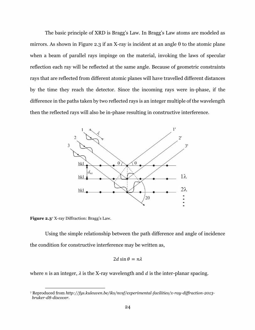


![FERROELECTRIC RAM [FRAM] - Study Mafia · A hysteresis loop for a ferroelectric capacitor, as shown in Fig. 4, displays the total charge on the capacitor as a function of the applied](https://static.fdocuments.us/doc/165x107/60399806255de32aec03d4cc/ferroelectric-ram-fram-study-mafia-a-hysteresis-loop-for-a-ferroelectric-capacitor.jpg)


