Growth and Properties of the Dilute Bismide …mbelab/bismide_growth_and_properties.pdf · 220 200...
26
Growth and Properties of the Dilute Bismide Semiconductor GaAs 1-x Bi x Introduction • Bismuth as a surfactant in semiconductor epitaxy • Electronic structure of bismide alloys • Transport properties • Unsolved problems • Outline of Presentation T. Tiedje University of British Columbia
Transcript of Growth and Properties of the Dilute Bismide …mbelab/bismide_growth_and_properties.pdf · 220 200...

Growth and Properties of the Dilute Bismide Semiconductor GaAs1-xBix
Introduction•
Bismuth as a surfactant in semiconductor epitaxy•
Electronic structure of bismide alloys•
Transport properties•
Unsolved problems•
Outline of Presentation
T. Tiedje University of British Columbia

Introduction
Bi
Sb
As
P
N -
+
Group VBi is heaviest non-Radioactive element•
Non-toxic•
Strong tendency to surface segregate in MBE•
Large spin-orbit coupling•
Devices
Semiconductor alloys with temperature •insensitive bandgap (Oe, Kyoto)
Low threshold, low power HBT (Hase, Sony •US6936871, 2006)
Local strain compensator for nitrogen, solar •cells (Mascarenhas, NREL)

Bandgap bowing with Bi:88 meV/%Bi
Francoeur et al, APL 82 (2003)
Lattice constant 6.32 Å
GaBi
GaN
Giant Bandgap Bowing in Both Nitrides and Bismides
Tixier et al. APL 82, 2245 (2003)
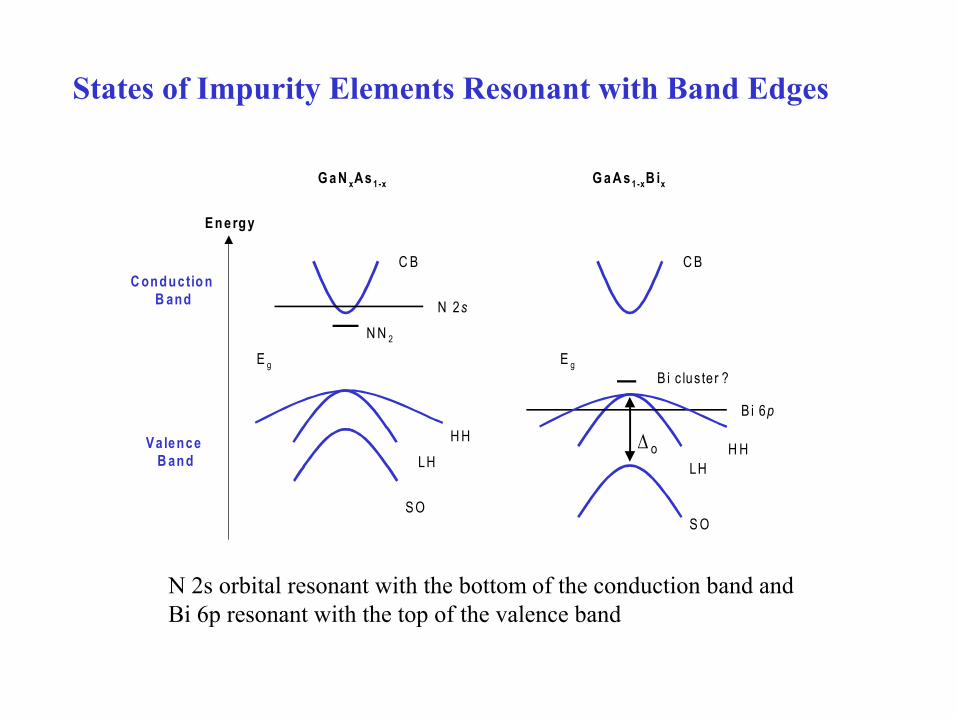
C onductio nB and
Va lenceB an d
E n e rg y
E g
N N 2
H H
N 2s
S O
LH
C B C B
G a N xAs 1-x G a A s 1-xB ix
S O
LH
B i c lus te r ?
B i 6p
H H
E g
∆ o
States of Impurity Elements Resonant with Band Edges
N 2s orbital resonant with the bottom of the conduction band and Bi 6p resonant with the top of the valence band
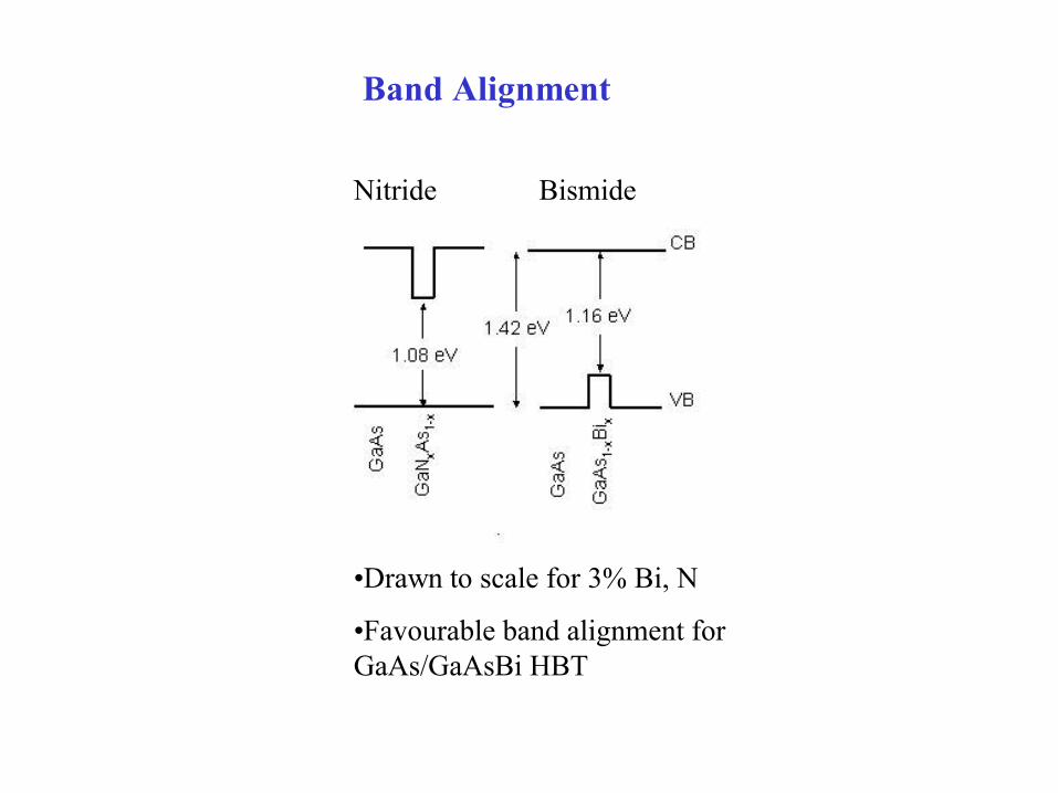
Band Alignment
Drawn to scale for 3% Bi, N•
Favourable band alignment for •GaAs/GaAsBi HBT
Nitride Bismide

Giant Bandgap Bowing Effect
Bismide Nitride
0 5%[Bi]
Linear interpolation
In bismides, 85 meV/% bandgap change much bigger than in •InGaAs which is 11 meV/%
>100 meV/% in dilute nitride, opposite sign!•E. Nodwell et al Phys Rev. B 155210 (2004)
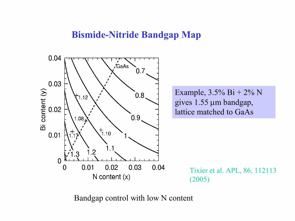
Bismide-Nitride Bandgap Map
Bandgap control with low N content
Example, 3.5% Bi + 2% N gives 1.55 µm bandgap, lattice matched to GaAs
Tixier et al. APL, 86, 112113 (2005)

VG-V80H solid source MBE deposition system•
Helical RF plasma source for nitrogen•
Conventional Knudsen effusion cell for Bi•
Bi BEP up to 10-5 Torr, 450-750oC•
incorporation < 2 x 1017 cm-3
Substrate temperatures 400oC - 600oC•
V/III flux ratio between 1 and 8•
GaAs Substrate
GaNAs Film ~225 nm
Surfactant MBE Growth of Dilute Nitrides

Surfactant Effect on Surface Morphology
No Bi FluxV/III ratio =1, rms ~ 1.2 nm
Vertical scale: 10 nm
High Bi Flux (~10-5 torr)V/III ratio =1, rms ~ 0.1 nm
Vertical scale: 0.8 nm
2 x 2 µm AFM images GaN0.004As0.996
Step flow growth at 460C, no Bi incorporation in SIMS•
Ideal surfactant?• Tixier et al., J. Cryst. Growth 251 (2003), 449

220
200
180
160
140
120
100
Spe
cula
r RH
EE
D In
tens
ity (a
rb. u
nits
)
140120100806040200time (s)
Substrate Temperature (°C)440 452 475 505 560
Measurement of Bi Coverage with RHEED
Desorption
Open Bi Close Bi
Change to 3x1 reconstruction with Bi flux•Specular intensity increases with Bi coverage•
Bi Flux = 1x10⁻⁶ torr

1.0
0.8
0.6
0.4
0.2
0.0
Bi C
over
age
(ML)
3.0x10-62.01.00.0Bi Flux (Torr)
modified langmuir modelRHEED data
Pressure Dependence of Bi Coverage
U = 1 eVzε = 0.2 eV
1.0
0.8
0.6
0.4
0.2
0.0
Bi C
over
age
(ml)
700650600550500450Bismuth cell temperature (°C)
Open BiClose Bi
Tsubs = 460oC

Langmuir Model for Bi Surface Coverage
Langmuir isotherm modified to include attractive Bi-Bi •interactions on surface
θ - Bi surface coverageP - Bi pressureU - binding energy of Bi to the surfaceε - lateral Bi-Bi interaction energyz - coordination number of Bi
expoU zb b
kTεθ+ =
1bP
bPθ =
+

1.0
0.8
0.6
0.4
0.2
0.0
Bi c
over
age
(ML)
800700600500400Substrate temperature(°C)
modified langmuirRHEED data
Temperature Dependence of Bi Coverage
U = 1 eVzε = 0.2 eV
Langmuir isotherm modified for lateral interactions•
Surface binding energy, vapour pressure, close to liquid Bi
Surfactant layer similar to liquid Bi
E. C. Young et al. J. Cryst. Growth 279, 316 (2005)

Effect of Bi on Nitrogen Incorporation
102
103
104
105
106
107
108D
iffra
cted
Inte
nsity
( cp
s )
6004002000-200θ ( arcsec )
Increasing Bi fluxIncreasing [N]
(004) x-ray diffraction peaks
Unexpected behaviour as both N, Bi are group V, competing for lattice sites
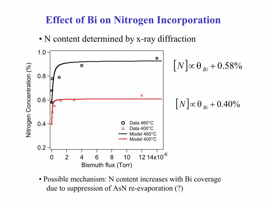
Effect of Bi on Nitrogen Incorporation
[ ] %58.0+∝ BiN θ
N content determined by x-ray diffraction•1.0
0.8
0.6
0.4
0.2
Nitr
ogen
Con
cent
ratio
n (%
)
14x10-6121086420Bismuth flux (Torr)
Data 460°CData 400°CModel 460°CModel 400°C
[ ] %40.0+∝ BiN θ
Possible mechanism: N content increases with Bi coverage• due to suppression of AsN re-evaporation (?)

Room Temperature Photoluminescence of InGaNAs:Bi QWs
1.0
0.8
0.6
0.4
0.2
0.0
RT
PL in
tens
ity (A
rb. u
nits
)
1400135013001250120011501100Wavelength (nm)
InGaNAs QWs (26% In; 1.1% N)
As GrownAnnealed at 730°C for 60s
With Bi (BEP ~10 -7Torr)
GaAs Substrate400 µm
InGaNAs QW
GaAs Cap~ 250 nm
low Bi flux ~ 10-7 torr•

Effect of Bi on PL SpectrumTemperature dependence of PL spectrum with and without Bi surfactant•
Low energy tail in PL reduced with Bi
0.54% N, no Bi 0.56% N, with Bi
Emission from Nx cluster states
Surfactant reduces density of localized N cluster statesD. Beaton, MSc Thesis UBC

Challenge of GaAsBi growth:
à avoid Bi and Ga droplet formation
5 x 5 µm scanVertical scale 350 nm
10 x 10 µm scanVertical scale 250 nm

Scat
tere
d Li
ght I
nten
sity
(au)
11x1031098765
Time (s)
5x10⁻⁷
4
3
2
1
Cham
ber Pressure (Torr)Open GaOpen Bi
Scattered light signalChamber pressure
In-situ Light Scattering Guides MBE Growth
As2 pressure
UV light scattering highly sensitive to metal (Ga, Bi) droplet formation•
Narrow process window•
Droplet formation
E. C. Young et al., Phys. Stat. Sol. (2007)

Diff
ract
ed In
tens
ity (
cps
)
200010000-1000-2000θ ( arcsec )
GaAs1-xBixx = 0.5%
GaAs1-xBixx = 1.9%
GaAs1-xBixx = 3%
Good Structural Quality
Vertical scale 3 nm rms roughness 0.205 nm Growth temp. 390 C !!
2 x 2 µm AFM
E. C. Young et al., PSS (2007)

14x103
12
10
8
6
4
2
0
RT
PL
Inte
nsity
(au)
14001300120011001000900800
Wavelength (nm)
GaAs1-xBix200 nm, x = 1.7%
GaAs1-xBix125 nm, x = 1.9%
GaAs1-xBix QW20 nm QW, x = 3.0%
10 layer MQW 5 nm InyGa1-yAs y = 20%
984 nm
1072 nm
962 nm
Bismides: Strong Room Temperature Photoluminescence
Efficient PL in low temperature grown material (T=360C), that is normally full of As antisites and poor electronic quality
Bismides
InGaAs QW
Ga GaBi
GaBiAs
GaBi As
In InN
InNN
GaN N
Ga
Light emitting center a •Bi cluster?
Indium cluster, light •emitting center in Ga(In)N
E. C. Young, PhD Thesis, UBC (2007)
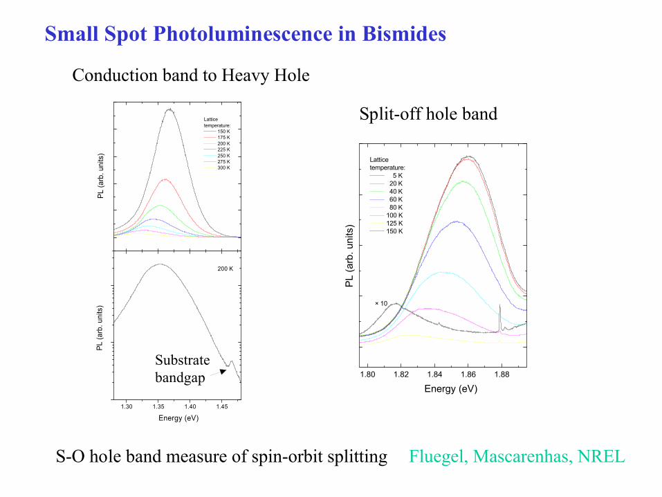
Latticetemperature:
150 K175 K200 K225 K250 K275 K300 K
PL (a
rb. u
nits
)
1.30 1.35 1.40 1.45
200 K
Energy (eV)
PL (a
rb. u
nits
)
1.80 1.82 1.84 1.86 1.88
× 10
Latticetemperature:
5 K20 K40 K60 K80 K
100 K125 K150 K
PL (a
rb. u
nits
)
Energy (eV)
Small Spot Photoluminescence in Bismides
Conduction band to Heavy Hole
Split-off hole band
Substrate bandgap
Fluegel, Mascarenhas, NRELS-O hole band measure of spin-orbit splitting

1.30
1.40
1.50
1.60
1.80
1.85 (a)
Band gap PL
Spin-Orbit PL
150 KPL
Ene
rgy
(eV)
0.0 0.5 1.0 1.5 2.00.30
0.40
0.50
(b)
SO s
plitt
ing
(eV)
Bi concentration (%)
“Giant” Increase in Spin-Orbit Splitting
Fluegel, Mascarenhas et al. PRL 97, 067205 (2006)
Increase in spin-orbit splitting in parallel with reduction in bandgap

Frequency Dependent Conductivity
Bismide: Drude-like Nitride: non-Drude
Conductivity is dominated by electrons•
Bismide result similar to host GaAs, nitride rather different, consequent •of N affect on the conduction band. Explanation?
Measured 10 ps after optical injection of ~1018 cm-3 e-h pairs

Terahertz Measurements of Electron Mobility
D. Cooke, F. Hegmann et al APL 89, 122103 (2006)
1% N has drastic effect on electron mobility, Bi has comparatively little effect

Conclusions
Dilute bismide semiconductors belong to a class of semiconductor •alloys with a dilute, impurity-like component, analogous to dilute nitrides (GaAsN) etc.
Bi is an ideal surfactant (no incorporation) under certain conditions, •improves structure and electronic properties, enables low temperature growth
Need for calculations of spin-orbit splitting in bismides, conduction •band and valence band
Promising device applications •
www.phas.ubc.ca/mbelab