Graphene Tutorial Dresselhaus - Epitaxial Graphene · PDF fileThis idea suggested that a...
63
M.A. Pimenta, UFMG Brazil A. Jorio, UFMG Brazil F. Plentz Filho, UFMG Brazil A. Souza Filho, UFC Brazil R. Capaz, UFRJ Brazil Paula Corio, USP Brazil Collaborators: G. Dresselhaus, MIT H. Son, MIT J. Kong, MIT M. Hofmann, MIT L.G. Cancado, Rochester G.G. Samsonidze, UC Berkeley M. Endo, Shinshu U R. Saito, Tohoku U J. Jiang, Tohoku U Y.A. Kim, Shinshu U M. Terrones, IPICYT, Mexico
Transcript of Graphene Tutorial Dresselhaus - Epitaxial Graphene · PDF fileThis idea suggested that a...
M.A. Pimenta, UFMG Brazil
A. Jorio, UFMG Brazil
F. Plentz Filho, UFMG Brazil
A. Souza Filho, UFC Brazil
R. Capaz, UFRJ Brazil
Paula Corio, USP Brazil
Collaborators: G. Dresselhaus, MIT
H. Son, MIT
J. Kong, MIT
M. Hofmann, MIT
L.G. Cancado, Rochester
G.G. Samsonidze, UC Berkeley
M. Endo, Shinshu U
R. Saito, Tohoku U
J. Jiang, Tohoku U
Y.A. Kim, Shinshu U
M. Terrones, IPICYT, Mexico

Outline
•!Historical Graphene to Graphene path
•! Carbon Nanotubes as Prototype Materials
•!Disordered Graphite
•!Graphene and Graphene Ribbons
•! Looking to the Future of Carbon Nanostructures
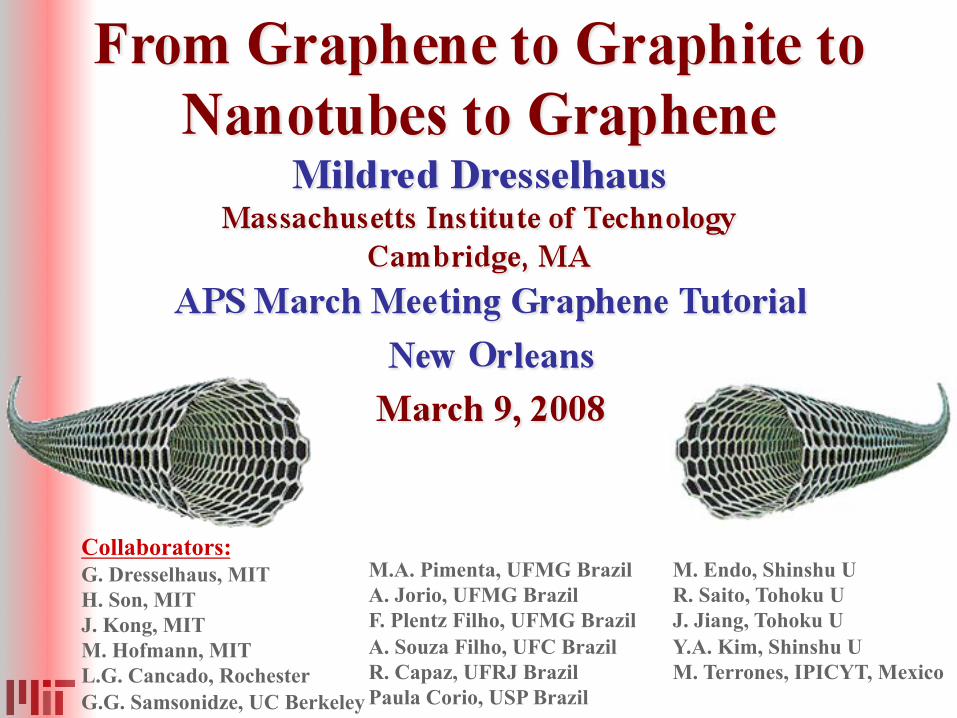
Graphene is the Mother of all
nano-Graphitic forms
•!A graphene sheet is one million times thinner (10-6) than a sheet of paper.
•!Graphene is a 2D building block material for other sp2 bonded carbon
materials. It can be wrapped up into 0D fullerenes, rolled into 1D nanotubes,
cut into 1D graphene ribbons or stacked into 3D graphite
0D 3D 1D
2D
1D
From graphene to graphite to fullerenes
to nanotubes to graphene
In the opening overview, we follow a path:
–!from the early work on graphene
–!to the developments in graphite
–!to graphite intercalation compounds
–!to fullerenes
–!to nanotubes
–!and then back to graphene

The Electronic Structure of Graphene is the
starting point for the electronic structure of graphite
P.R. Wallace, Phys. Rev. 71, 622 (1947)
(!0 values are from 2.9 to 3.1eV)
Near the K point
is the overlap integral between nearest neighbor "-orbitals
linear # relation
and
and
EF
where

2D Graphite (Graphene) unit cells
Direct lattice First Brillouin zone (BZ)

Energy bands of 2D Graphite
(graphene)
P. R. Wallace, Phys. Rev, 71 622 (1947).
•! ! bands of graphene
–!Unit Cell, B. Z.
B A
t
•! Graphene is a zero gap
semiconductor
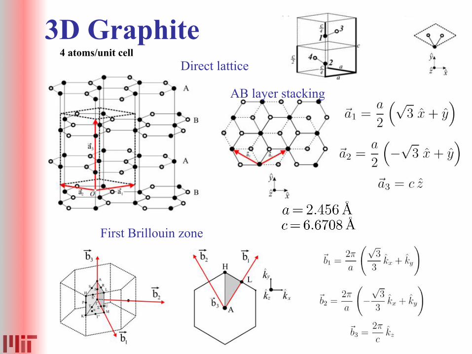
3D Graphite Direct lattice
First Brillouin zone
AB layer stacking
4 atoms/unit cell

Extension of Graphene to
Graphite •! McClure extended 2D graphene electronic structure calculation to 3D graphite.
•! Magneto-optical experiment measured energy bands of graphite at several regions of the Brillouin zone
(near K and H)
•! Experiment (1961) was enabled by the availability of a new material, highly oriented pyrolytic graphite (HOPG) Ubbelohde (1960)
•! Used symmetry-based E(k) model of McClure to yield band parameters for the electronic structure of graphite.
M.S. Dresselhaus and J.G. Mavroides. IBM Journal of Research and
Development 8, 262 (1964)
J.W. McClure, Phys. Rev. 108, 612 (1957); 119, 606 (1960)

Identification of Electrons and
Holes in Graphite
P.R.Schroeder, M.S. Dresselhaus and A.Javan, Phys.Rev. Lett 20,1292 (1968)
The locations of electrons and holes are incorrectly given in the
literature, prior to 1968. The effective masses for electrons and
holes in graphite are often used in the current graphene literature.
Using circular polarized radiation in the first magneto-optical
experiment to use a laser, the locations of electrons and holes in the
Brillouin zone were identified
Experiment showed that
electrons were located
near K (K’)

Spintronics in Graphene
•! An early paper by Gene Dresselhaus defined what is now known as the “Dresselhaus spin-orbit term” in III-V semiconductors {G. Dresselhaus, Phys. Rev. 71, 220 (1955)} with E(k) having a linear k-dependence. A model for the spin-orbit interaction in graphite as imposed by symmetry was developed {G. Dresselhaus & M.S. Dresselhaus, Phys. Rev. 140, A401 (1965)}
•! Since the spin-orbit interaction in graphite is very small, the spin lifetime in graphene can be very long. Therefore graphene has become an interesting material for studying spin transport.

Entry into the Nanoworld
•! Through the unexpected observation by Hannay
et al. at AT&T Bell Labs of superconductivity in
stage 1 graphite intercalation compounds (C8K) (Hannay et al, Phys.Rev.Lett. 14, 225 (1965)
much interest was aroused since neither
potassium nor carbon is superconducting
•! Intercalation compounds allowed early studies to be made of individual or few graphene layers in the environment of the intercalant species.
C8K

Low Dimensional Science Studies in
Graphite Intercalation Compounds
(1973-1993) Magnetoreflection
Transport
Raman
Optical
Structural
Magnetic
Superconductivity
Studies on single or few layer Graphene were
carried out in the environment of the
intercalant species were carried out by many
researchers

Concurrent Studies on Forerunners to Fullerenes
•! Liquid carbon studies (1983)
Liquid carbon was found to be metallic
T. Venkatesan et al, Phys. Rev. Lett. 53, 360 (1984)
•! The Laser ablation process used to make liquid carbon
produced large clusters (like C100) rather than C2 or C3
E.A.Rohlfing, D.M. Cox and A.Kaldor. J.
Chem.Phys., 81, 332 (1984)
Cx
liquid carbon
Laser
graphite
•! Trip to Exxon Research Lab to
discuss results.
•! Soon Exxon published famous result showing
mass spectroscopy intensity vs numbers of C
atoms in clusters with peaks at C60 and C70
•! The Exxon result led to the discovery of
fullerenes by Kroto, Smalley and Curl (1985)
Intercalation led to ion implantation and laser irradiation of graphite

Forerunners of Carbon Nanotubes
•! Vapor grown carbon fibers
•! At center of these carbon fibers is a multiwall carbon nanotube
•! A connection between fullerenes and nanotubes was made by going from C60!C70!C80!nanotubes
•! This idea suggested that a single wall Carbon nanotube would
be interesting (August 1991) and led to calculating the
electronic structure of SWNTs before they were ever seen
M.S.Dresselhaus et al., Graphite Fibers and Filaments, Springer (1988)
Saito, Fujita, Dresselhaus2, Electronic structure of carbon fibers based on C60,
C60 C70 C80
CNT
PRB 46, 1804 (1992)

Unique One Dimensional (1D) Properties
•! High aspect ratio
•! Enhanced density of states in 1D
•! Molecular behavior (spikes in DOS)
•! Solid state behavior (tails in DOS)
3D
Bulk Semiconductor
2D
Quantum Well
1D
Quantum Wire
0D
Quantum Dot
D. O
. S
.
D. O
. S
.
D. O
. S
.
D. O
. S
.
Carbon nanotubes and nanoribbons have:

General Relations between 1D and 2D Systems
shown in terms of carbon nanotubes
1D van Hove singularities
give high density of
electronic states (DOS) at
well defined energies
Rolling up a 2D sheet Confinement of 1D electronic states
on cutting lines
"! Carbon nanotubes are metallic if cutting line passes through the K point
"! Otherwise they are semiconducting
1D 2D

•! Small size: ~1 nm diameter (down to
~10 atoms around the circumference)
•! Electronic Properties: can be either
metallic or semiconducting depending
on diameter and orientation of the
hexagons
•! Mechanical: Very high strength,
modulus, and resiliency.
•! Physics: model system for1D density
of electronic states.
•! Single molecule Raman spectroscopy,
luminescence and transport properties.
chiral
zigzag
armchair
graphene ribbon SWNT
Outline
•!Historical Graphene to Graphene path
•! Carbon Nanotubes as Prototype Materials
•!Disordered Graphite
•!Graphene and Graphene Ribbons
•! Looking to the Future of Carbon Nanostructures

(4,2)
Nanotube Structure in a Nutshell
Rolled-up graphene layer
with a large unit cell.
Graphene Sheet SWNT
Each (n,m) nanotube is a unique molecule
R.Saito et al, Imperial College Press, 1998

Armchair Nanotube
(5,5)
(9,0)
(6,5)
Zigzag Nanotube
Chiral Nanotube
Carbon Nanotubes
Hemispherical fullerene caps are shown for armchair and zigzag nanotubes

Energy Bands of Nanotubes
•! N one-dimensional electronic energy bands
(5,5) (9,0) (10,0)
R. Saito et al., Phys. Rev. B46, 1804 (1992)

Metallic Carbon Nanotubes
•! 1D Energy Dispersion of SWNT
–!K point is always on a cutting line
–!Two inequivalent neighboring cutting lines ---
cause splitting in the density of states
Trigonal warping effect
R. Saito et al, Phys. Rev. B61, 2981(2000)

Semiconducting Carbon Nanotubes
•! K points are always at 1/3 (or 2/3) position
–!Two neighboring lines contribute to different
energies
–!No DOS splitting for any chirality DOS(10,0)
R. Saito et al, Phys. Rev. B61, 2981(2000)
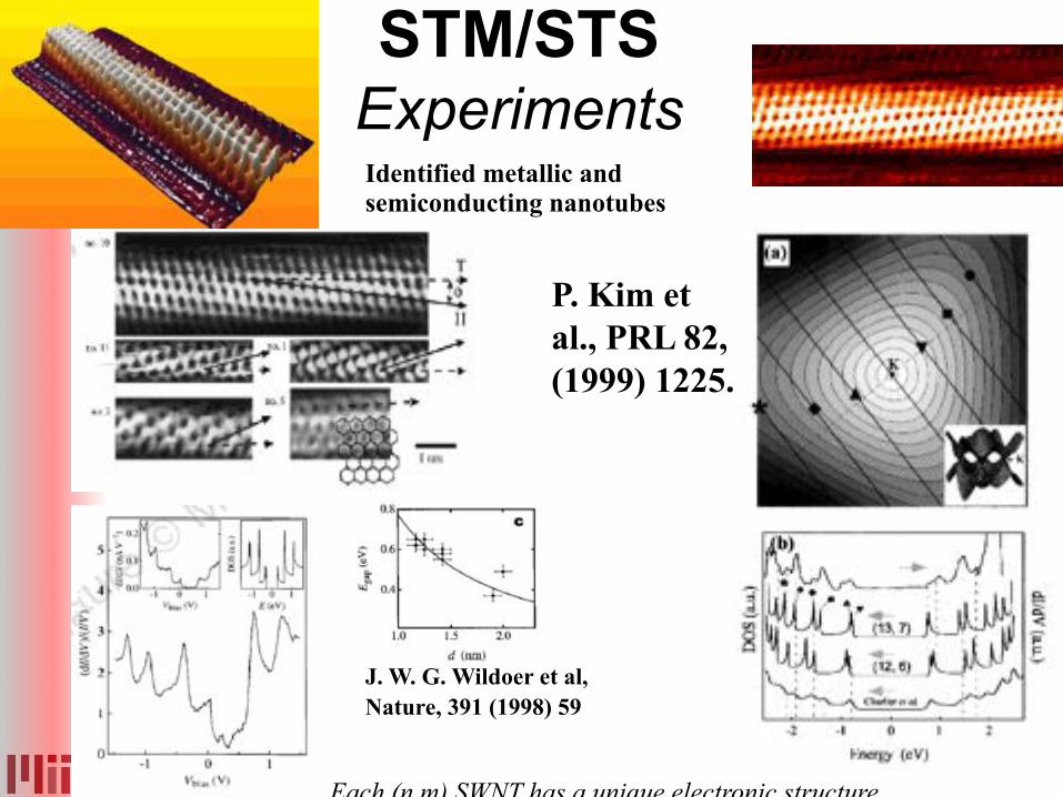
STM/STS Experiments
J. W. G. Wildoer et al,
Nature, 391 (1998) 59
P. Kim et
al., PRL 82,
(1999) 1225.
Identified metallic and semiconducting nanotubes
Each (n,m) SWNT has a unique electronic structure
E = 0.94eV
= 1.17eV
= 1.58eV
= 1.92eV
= 2.41eV
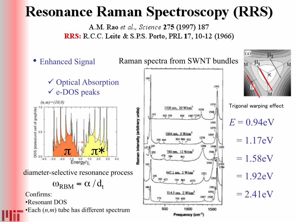
Raman spectra from SWNT bundles
"$ "!$
•! Enhanced Signal
#! Optical Absorption
#! e-DOS peaks
diameter-selective resonance process
%RBM = & / dt
"#$%&'()*+(#,$'%*-..-/0!
Confirms:
•!Resonant DOS
•!Each (n,m) tube has different spectrum

dt = 1.37 ± 0.18 nm
G-band resonant Raman spectra Diameter dependence of
the Van-Hove singularities laser energy
G-band
Kataura plot
Metallic and semiconducting tubes have different lineshapes

Therefore the geometrical structure of an individual
carbon nanotube can be found by Raman spectroscopy
A. Jorio (UFMG) et al., Phys. Rev. Lett. 86, 1118 (2001)
RBM
Semiconducting
Metallic
R. Saito et al.,
Phys. Rev. B 61, 2981 (2000)
'
Each nanotube has a
unique DOS because of
trigonal warping effects
(%RBM, Eii) !
(n,m)

Raman Spectra of SWNT Bundles
Raman Shift (cm11)
Ram
an I
nte
nsi
ty
o
G+
Metallic G-band
G-
RBM: !RBM' 1/dt D-band
G-band
G+
G-
G"-band
•!RBM gives tube diameter and diameter distribution
•!Raman D-band characterizes structural disorder
•!G- band distinguished M, S tubes and G+ relates to charge transfer
•!G! band (2nd order of D-band) provides connection of phonon to its wave vector
•!Each feature in the Raman spectra provides complementary information about nanotubes

Water, 1.1 g/cm3
1.0 g/cm3
SDS
1.2 g/cm3
e-DOS of (n, m) = (10,5)
absorption fluorescence
v1
v2
c1
c2
Band Gap Fluorescence M. J. O’Connell et al., Science 297 (2002) 593
S. M. Bachilo et al., Science 298 (2002) 2361.
Good method to determine the (n,m) of
semiconducting nanotubes in a given sample
SDS=Sodium Dodecyl Sulfate
Emission (nm)
Exci
tati
on (
nm
) Peaks only

2-photon excitation to a 2A+ symmetry exciton (2p)
and 1-photon emission from a 1A1 exciton (1s)
cannot be explained by the free electron model
Wang et al. Science 308, 838 (2005)
(7,5)
(6,5)
(8,3)
(9,1) E11
(1s)
2-PHOTON EXCITATION ENERGY
1.4
1.3
1.2`
1.2 1.4 1.6 1.8
EM
ISS
ION
EN
ER
GY
1A1$
BAND-EDGE
2-PHOTON EXCITATION ENERGY
1.2 1.4 1.6 1.8 2.0
AB
SO
RP
TIO
N (
a.u.)
E11 (1s)
1A1$E11
(2p) 2A+$
Experimental Justification for excitons
Excitons in Carbon Nanotubes
The observation that excitation and emission are
at different frequencies supports exciton model rather
than free electron model
Outline
•!Historical Graphene to Graphene path
•! Carbon Nanotubes as Prototype Materials
•!Disordered Graphite
•!Graphene and Graphene Ribbons
•! Looking to the Future of Carbon Nanostructures

G band: Raman spectra of graphitic
materials: defect detection.
G" band: Second
harmonic of D band.
(also called 2D band)
Defect-induced
D band:
( iTO mode at the K point )
Tuinstra and Koenig, J. Chem. Phys. 53, 1126 (1970).
Nemanich and Solin, Solid State Comm. 23, 417 (1977).
Tsu et al., Solid State Commun. 27, 507 (1978).
Symmetry-breaking
Nanostructured graphite
with defects

Intravalley double-resonance process
Explains the D" band process
Baranov et al., Opt. Spectrosc. USSR 62, 612 (1987).
Thomsen and Reich, Phys. Rev. Lett. 85, 5214 (2000).

Intervalley double-resonance process Explains the origin of the D-band
Saito et al., Phys. Rev. Lett. 88, 027401 (2002).
Scattering by defect in an energy conserving process

D"
G band: first order allowed (closed to the ( point).
D" band: double resonance intravalley process.
D and G" bands: double resonance intervalley process.
Intravalley vs. intervalley
double-resonance processes
D G"
Saito et al., Phys. Rev. Lett. 88,
027401 (2002).

Determination of the average crystallite
size La of nanographite films by
STM and X-ray diffraction using sychrotron radiation
The values of La obtained by
STM and X-ray diffraction are
in good agreement:
Cançado et al., App. Phys. Lett. 88, 163106 (2006).
The same samples are used for Raman characterization of La

Dependence of the ratio ID / IG on the crystallite size La in the
Raman spectra of disordered graphite
Tuinstra and Koenig, J. Chem. Phys. 53, 1126 (1970).
Tuinstra and Koenig, J. Compos. Mater 4, 492 (1970).
!! = 4.4nm for ) = 514.5 nm (2.41eV)
Knight and White, J. Mater. Res. 4, 385 (1989).
Cançado et al.,
App. Phys. Lett. 88,
163106 (2006).

Dependence of the ratio ID / IG on the excitation laser
energy El in the Raman spectra of disordered graphite
Mernagh et al., Carbon 22, 39 (1984).
Cançado et al., App. Phys. Lett. 88, 163106 (2006).

General equation for the determination of the crystallite
size La of nanographite by Raman spectroscopy
Cançado et al., Appl. Phys. Lett. 88, 163106 (2006).

Measuring the dependence of the differential cross section of the
Raman bands in graphite on the excitation laser energy El
Cançado et al., Phys. Rev. B. 76, 064304 (2007).
Normalized to G-band intensity Direct intensity measurement
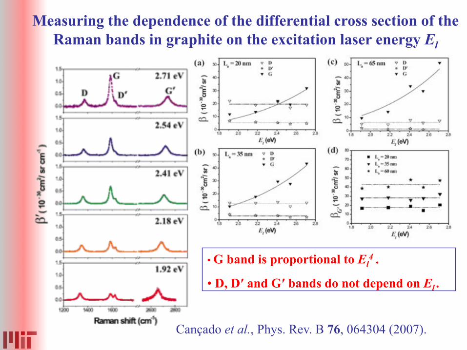
•! G band is proportional to El4 .
•! D, D" and G" bands do not depend on El .
Cançado et al., Phys. Rev. B 76, 064304 (2007).
Measuring the dependence of the differential cross section of the
Raman bands in graphite on the excitation laser energy El

Cançado et al., Carbon 46, 272 (2008).
Quantifying the stacking order in
nanographites by Raman spectroscopy

Outline
•!Historical Graphene to Graphene path
•! Carbon Nanotubes as Prototype Materials
•!Disordered Graphite
•!Graphene and Graphene Ribbons
•! Looking to the Future of Carbon Nanostructures

Electronic structures of graphene and bilayer graphene
Sylvain Latil and Luc Henrard, Phys. Rev. Lett. 97, 036803 (2006).
Taisuke Ohta, et al., Science 313, 951 (2006).
Linear E~k parabolic E~k2

Raman G" band identifies the number of layers G! (3D graphite) – two peaks
G! (2D graphite) – one peak
•!Ferrari et al., Phys. Rev. Lett. 97, 187401 (2006).
•! Gupta et al., Nanoletters 6, 2667 (2006).
•! Graf et al., Nanoletters, (2007).
Distinguishes graphite from graphene
Identifies the number of graphene layers

Raman confocal image of single graphene layer
The D band is detected only at the edges in
contrast to the G-band and G"-band.
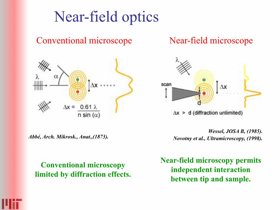
Near-field optics
Conventional microscope Near-field microscope
Near-field microscopy permits
independent interaction
between tip and sample.
Abbé, Arch. Mikrosk., Anat.,(1873). Wessel, JOSA B, (1985).
Novotny et al., Ultramicroscopy, (1998).
Conventional microscopy
limited by diffraction effects.

STRUCTURAL DEFECTS IN BURIED NANOTUBES
Topography:
Structural variations (defects, branching, .. ) hidden in confocal imaging !
Nano Lett. 6, 744 (2006).
Near-field Raman: Confocal Raman:

Out-of-plane modes show larger
enhancement than in-plane modes:
L.G.Cancado, unpublished work
In near field optics

Graphene Ribbons Armchair Zigzag
•!Special feature of graphene ribbons is that they have edges and few
columns of carbon atoms along the width.
Direction of
cutting lines
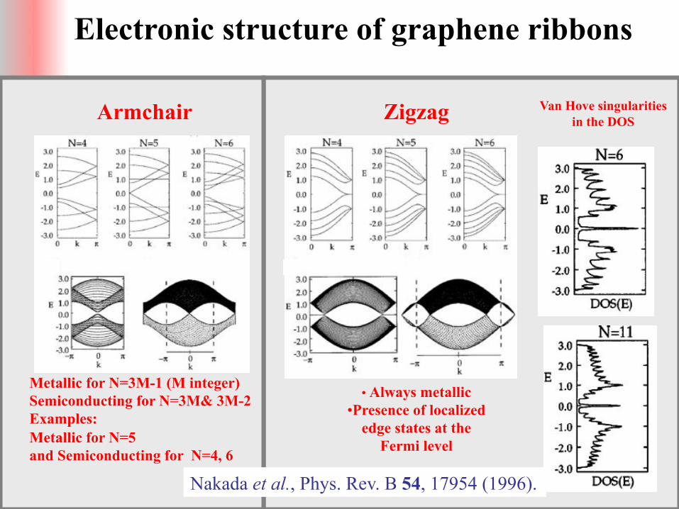
Electronic structure of graphene ribbons
Armchair Zigzag
Metallic for N=3M-1 (M integer)
Semiconducting for N=3M& 3M-2
Examples:
Metallic for N=5
and Semiconducting for N=4, 6
•! Always metallic
•!Presence of localized
edge states at the
Fermi level
Van Hove singularities
in the DOS
Nakada et al., Phys. Rev. B 54, 17954 (1996).
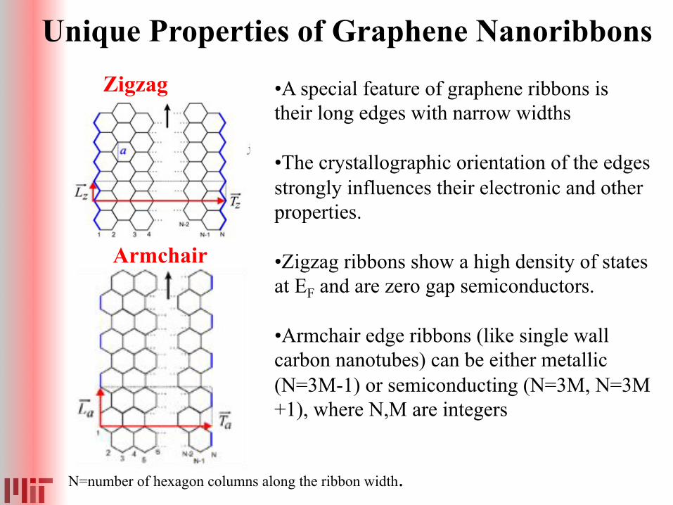
Unique Properties of Graphene Nanoribbons
Armchair
Zigzag •!A special feature of graphene ribbons is
their long edges with narrow widths
•!The crystallographic orientation of the edges
strongly influences their electronic and other
properties.
•!Zigzag ribbons show a high density of states
at EF and are zero gap semiconductors.
•!Armchair edge ribbons (like single wall
carbon nanotubes) can be either metallic
(N=3M-1) or semiconducting (N=3M, N=3M
+1), where N,M are integers
N=number of hexagon columns along the ribbon width.

Raman structure used to Identify graphene nanoribbons
Synthesis:
•! Electrophoretic deposition of nano-diamond particles on a HOPG substrate.
•! At a HTT of 16000C, the nano-diamond particles are graphitized, forming
nanographite sheets and ribbons.
Affoune et al., Chem. Phys. Lett. 348, 17 (2001), Langmuir 17, 547 (2001) .
STM image of a
zigzag ribbon:
AFM image of a graphene
nanoribbon: AFM image of many
graphene nanoribbons
parallel to each other:
Cançado et al., Phys. Rev. Lett. 93, 047403 (2004).

Cançado et al., Phys. Rev. Lett. 93, 047403 (2004).
Raman spectra of graphene nanoribbons
Gruneis et al., Phys. Rev. B 67, 165402 (2003).
G1 - graphene nanoribbon
G2 - HOPG substrate

Influence of the atomic structure in the
Raman spectra of graphite edges
ID1 > ID2
ID!1 ~ ID!2
Cançado et al., Phys. Rev. Lett. 93, 247401 (2004).
Influence of the atomic structure in the Raman
spectra of graphite edges
Cançado et al., Phys. Rev. Lett. 93, 247401 (2004).
Edge 1:
Armchair
Edge 2:
Zigzag
The D band Raman spectra are
used to distinguish between
armchair and zigzag edges

Outline
•!Historical Graphene to Graphene path
•! Carbon Nanotubes as Prototype Materials
•!Disordered Graphite
•!Graphene and Graphene Ribbons
•! Looking to the Future of Carbon Nanostructures
Outlook
•! 1D carbon nanotubes continue to be an expanding
field, now focusing more heavily on applications
•! 1D carbon nanoribbons is a newly emerging field
that is expected to grow rapidly in the near future,
particularly if higher quality ribbons can be made.
•! The synergy between nanotubes, graphene and
nanoribbons will surely enrich one another strongly
in advancing both their nanoscience and applications.

Potential Applications of Carbon Nanotubes
Chapter by M. Endo, M. S. Strano, P. M. Ajayan @ Springer
TAP111
Large Volume Applications Limited Volume Applications
(Mostly based on Engineered
Nanotube Structures)
Present - Battery Electrode Additives (MWNT)
- Composites (sporting goods; MWNT)
-!Composites (ESD* applications; MWNT)
-!(*ESD – Electrical Shielding Device)
- Scanning Probe Tips (MWNT)
- Specialized Medical Appliances
(catheters) (MWNT)
Near Term
(less than ten
years)
- Battery and Super-capacitor Electrodes
-! Multifunctional Composites
-! Fuel Cell Electrodes (catalyst support)
- Transparent Conducting Films
- Field Emission Displays / Lighting
- CNT based Inks for Printing
- Single Tip Electron Guns
- Multi-Tip Array X-ray Sources
- Probe Array Test Systems
- CNT Brush Contacts
- CNT Sensor Devices
- Electro-mechanical Memory Device
- Thermal Management Systems
Long Term
(beyond ten
years)
- Power Transmission Cables
- Structural Composites (aerospace and
automobile etc.)
- CNTs in Photovoltaic Devices
- Nano-electronics (FET,Interconnects)
- Flexible Electronics
- CNT based bio-sensors
- CNT Fitration/Separation Membranes
- Drug-delivery Systems
More emphasis now is on applications

Outlook
•! 1D carbon nanotubes continue to be an expanding
field, now focusing more heavily on applications
•! 1D carbon nanoribbons is a newly emerging field
that is expected to grow rapidly in the near future,
particularly if higher quality ribbons can be made.
•! The synergy between nanotubes, graphene and
nanoribbons will surely enrich one another strongly
in advancing both their nanoscience and applications.
Outlook

The End