
Graphene Travelling Wave Ampli er for Integrated ...
168
Graphene Travelling Wave Amplifier for Integrated Millimeter-Wave/Terahertz Systems by Naimeh Ghafarian A thesis presented to the University of Waterloo in fulfillment of the thesis requirement for the degree of Doctor of Philosophy in Electrical and Computer Engineering Waterloo, Ontario, Canada, 2018 c Naimeh Ghafarian 2018
Transcript of Graphene Travelling Wave Ampli er for Integrated ...

Graphene Travelling Wave Amplifierfor Integrated
Millimeter-Wave/Terahertz Systems
by
Naimeh Ghafarian
A thesispresented to the University of Waterloo
in fulfillment of thethesis requirement for the degree of
Doctor of Philosophyin
Electrical and Computer Engineering
Waterloo, Ontario, Canada, 2018
c© Naimeh Ghafarian 2018

Examining Committee Membership
The following served on the Examining Committee for this thesis. The decision of theExamining Committee is by majority vote.
External Examiner: Mona JarrahiProfessor, Dept. of Electrical and Computer Engineering,University of California Los Angeles
Supervisor: Safieddin Safavi-NaeiniProfessor, Dept. of Electrical and Computer Engineering,University of Waterloo
Supervisor: Amir Hamed MajediProfessor, Dept. of Electrical and Computer Engineering,University of Waterloo
Internal Member: Dayan BanProfessor, Dept. of Electrical and Computer Engineering,University of Waterloo
Internal Member: Simarjeet SainiAssociate Professor, Dept. of Electrical and Computer Engineering,University of Waterloo
Internal-External Member: Zoran MiskovicProfessor, Dept. of Applied Mathematics,University of Waterloo
ii

I hereby declare that I am the sole author of this thesis. This is a true copy of the thesis,including any required final revisions, as accepted by my examiners.
I understand that my thesis may be made electronically available to the public.
iii

Abstract
Terahertz (THz) technology offers exciting possibilities for various applications, includ-ing high resolution biomedical imaging, long-wavelength spectroscopy, security monitoring,communications, quality control, and process monitoring. However, the lack of efficienthigh power easy-to-integrate sources and highly sensitive detectors has created a bottle-neck in developing THz technology. In an attempt to address this issue, this dissertationproposes a new type of graphene-based solid state travelling wave amplifier (TWA).
Inspired by the unique properties of electrons in graphene two-dimensional (2D) fluid,the author proposes a new type of TWA in which graphene acts as the sheet electron beam.These properties include higher mobility and drift velocity at room temperature, zero effec-tive mass, relativistic behavior, and a truly 2D configuration. Since the plasma propertiesof 2D electron fluid become more pronounced as the effective mass of electrons decreasesand electron mobility increases, THz devices based on graphene with massless quasiparti-cles significantly outperform those made of relatively standard semiconductor heterostruc-tures. Another significant advantage of graphene over semiconductors is that while thehigh drift velocity and electron mobility of semiconductors 2D electron gas (2DEG) areachieved only at very low temperatures, graphene has high mobility and drift velocity atroom temperature.
This thesis describes the theoretical and practical methods developed for the analysis,design, and fabrication of a graphene-based THz TWA. It investigates the interaction be-tween the electromagnetic wave and the drifting plasma wave in graphene by two methods.In the first approach, electrons in graphene are modelled as a 2D Fermi liquid, and thehydrodynamic model derived from a relativistic fluid approach is used to find the conduc-tivity. In the second approach, the travelling wave interaction is analyzed using a quantummechanical model. The drifting Fermi distribution function is applied to the linear con-ductivity response function of graphene obtained from random phase approximation. Theconductivity of graphene is obtained as a function of frequency, wave number, chemicalpotential, and drift velocity. The result is consistent with the hydrodynamic approach.Both methods show that negative conductivity, and thus gain, is obtained when the driftvelocity is slightly greater than the phase velocity. It is shown that the two methodsproduce comparable results.
In the next step, a slow-wave grating structure is designed and an estimate of theactual gain is obtained for the proposed graphene TWA structures. The Floquet modeanalysis of top grated slab and rectangular silicon waveguides is presented. Here, a newtheoretical method is developed to accurately estimate the field distribution of the first
iv

order space harmonic of a hybrid mode inside a periodic top-grated rectangular dielectricwaveguide. This method gives explicit expressions for the interaction impedance of theslow wave grating structures that are then used to design the waveguide and the grating.To verify the proposed approximation method, the results obtained with this approach arecompared with the simulation results.
Finally, a prototype structure is fabricated. The recipes developed for different partsof the structure are presented. These parts include: a nanometer size grating, a sub-millimeter dielectric waveguide, and biasing contacts on top of the graphene layer. Thedeveloped recipes ensure reliable fabrication processes for large-area graphene devices. Inaddition, two different methods used to fabricate long uniform gratings are compared. Thiswork ends by showing the measurement results obtained for the fabricated devices.
v

Acknowledgements
I would like to thank my supervisors, Prof. Safieddin Safavi-Naeini and Prof. HamedMajedi, for their patience, guidance and support. I would especially like to express mygratitude to Prof. Safavi-Naeini whose diverse and deep knowledge and intuition made myPhD studies a highly enriching experience. He gave me motivation and enough freedom totry and explore my ideas and pushed me forward in times of disappointment and when Idoubted my work would have a successful outcome.
It is also my pleasure to thank my PhD committee members, Prof. Zoran Miskovic,Prof. Dayan Ban, Prof. Simarjeet Saini, and Prof. Sujeet Chauhuri. I sincerely appreciateProf. Mona Jarrahi (University of California Los Angeles) for agreeing to be my externalexaminer.
I spent much of my PhD working at the Quantum Nano Center (QNC) fabricationfacility. Starting with no experience, I learned a great deal from Dr. Nathan Fitzpatrik,Brian Goddard and Rod Salandanan. I am especially indebted to Dr. Mohsen Raeiszadehwho gave me far more help than I expected, and is the source for almost all I now knowabout fabrication. I am also indebted to Dr. Anita Fadavi, Dr. Hadi Amarloo and Dr.Nazy Ranjkesh for helping me through the fabrication challenges by sharing their valuableexperiences.
I also would like to thank all of my friends and colleagues at the Center for IntelligentAntenna and Radio Systems (CIARS) with special thanks to: Dr. Aidin Taeb and Dr.Ahmad Ehsandar who kindly supported me not only technically with the VNA and millingmachine systems and the design of the measurement holder, respectively but also by actingas my living reference book with their advices; Dr. Suren Gigoyan who kindly help me in themeasurements; Dr. Behrooz Semnani for the fruitful discussions we have; Ardeshir Palizbanand Mohammad Fereidani for their help and advice in the packaging; and Dr. Arash Rohanifor the experience I gained in practical optics through projects we did together.
I also want to thank Mary McPherson not only for revising my thesis but also, and moreimportantly, for giving me the courage and confidence I needed for writing. Last but notleast I want to thank all the friends who created joyful moments for me during the courseof this PhD and made my life in Waterloo pleasant. Special thanks to my dearest friendsFarinaz Forouzannia, Maryyeh Chehresaz, Elnaz Barshan, and Neda Mohammadizadeh.
Words cannot express the deep gratitude I have to my parents for the sacrifice theyhave made for me. I owe all my success and happiness to them. Then, there is the joy ofmy life and warm center of our family, my brother. Thank you for being there, Mehdi.
vi

Dedicated to my parents;
Tayebeh Abdellahi and Mahmood Ghafarian.
vii

Table of Contents
List of Figures xi
1 Introduction 1
1.1 THz gap . . . . . . . . . . . . . . . . . . . . . . . . . . . . . . . . . . . . . 1
1.2 THz sources . . . . . . . . . . . . . . . . . . . . . . . . . . . . . . . . . . . 2
1.3 Semiconductor travelling wave amplifiers . . . . . . . . . . . . . . . . . . . 5
1.3.1 Graphene . . . . . . . . . . . . . . . . . . . . . . . . . . . . . . . . 6
1.4 Newly proposed graphene-based device . . . . . . . . . . . . . . . . . . . . 8
1.5 Analysis of the grating structure . . . . . . . . . . . . . . . . . . . . . . . . 9
1.6 Objectives and research overview . . . . . . . . . . . . . . . . . . . . . . . 10
2 Introduction to graphene 12
2.1 Graphene lattice structure . . . . . . . . . . . . . . . . . . . . . . . . . . . 12
2.2 Graphene Hamiltonian and energy band structure . . . . . . . . . . . . . . 13
2.3 Relativistic Dirac equation . . . . . . . . . . . . . . . . . . . . . . . . . . . 14
2.4 Comparison between Graphene 2DEG and semiconductor 2DEG . . . . . . 15
2.5 Graphene surface plasmon polariton waveguide . . . . . . . . . . . . . . . 16
2.5.1 Two-layer structure . . . . . . . . . . . . . . . . . . . . . . . . . . . 21
3 Quantum mechanical analysis of travelling wave amplification in graphene 25
3.1 Conclusion . . . . . . . . . . . . . . . . . . . . . . . . . . . . . . . . . . . . 33
viii

4 Hydrodynamic model of graphene 34
4.1 Conclusion . . . . . . . . . . . . . . . . . . . . . . . . . . . . . . . . . . . . 40
5 Analysis of travelling-wave amplifier using graphene 43
5.1 Analysis of general coupling in a periodic structure . . . . . . . . . . . . . 44
5.2 Analysis of Floquet modes in a slab dielectric waveguide with a grating ontop . . . . . . . . . . . . . . . . . . . . . . . . . . . . . . . . . . . . . . . . 47
5.2.1 First-order space harmonic . . . . . . . . . . . . . . . . . . . . . . . 50
5.2.2 Gain and dispersion equations . . . . . . . . . . . . . . . . . . . . . 51
5.3 Analysis of graphene traveling wave amplifier on a rectangular dielectricwaveguide . . . . . . . . . . . . . . . . . . . . . . . . . . . . . . . . . . . . 54
5.3.1 Analysis of Floquet modes in a rectangular dielectric waveguide witha grating on top . . . . . . . . . . . . . . . . . . . . . . . . . . . . . 60
5.3.2 Derivation of the field distribution of the first-order space harmonic 67
5.3.3 Gain and dispersion equations . . . . . . . . . . . . . . . . . . . . . 70
5.3.4 Verifying the proposed method using numerical simulation . . . . . 74
5.4 Conclusion . . . . . . . . . . . . . . . . . . . . . . . . . . . . . . . . . . . . 79
6 Fabrication and measurement 82
6.1 Fabrication of the grating . . . . . . . . . . . . . . . . . . . . . . . . . . . 87
6.2 Transfer of the graphene layer and fabrication of the DC bias contacts . . . 94
6.3 Fabrication of the silicon waveguide . . . . . . . . . . . . . . . . . . . . . . 106
6.4 Measurement results . . . . . . . . . . . . . . . . . . . . . . . . . . . . . . 114
6.5 Conclusion . . . . . . . . . . . . . . . . . . . . . . . . . . . . . . . . . . . . 116
7 Conclusion 117
7.1 Future work . . . . . . . . . . . . . . . . . . . . . . . . . . . . . . . . . . 118
APPENDICES 122
ix

A Tight-binding approach 123
A.1 Electronic structure of graphene . . . . . . . . . . . . . . . . . . . . . . . . 124
B Coupled-mode analysis of Floquet eigenmodes 127
C Marcatili’s method 130
D Improved Marcatili’s method 136
References 138
x

List of Figures
1.1 Applications of THz technology [1]. . . . . . . . . . . . . . . . . . . . . . . 2
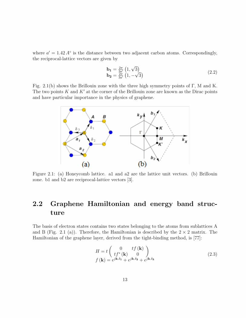
1.2 Compact THz sources. The Pf 2=constant line is the power-frequency slopeexpected for radio frequency devices; and the Pλ=constant line is the ex-pected slope for some commercial lasers [2]. . . . . . . . . . . . . . . . . . 3
2.1 (a) Honeycomb lattice. a1 and a2 are the lattice unit vectors. (b) Brillouinzone. b1 and b2 are reciprocal-lattice vectors [3]. . . . . . . . . . . . . . . . 13
2.2 Energy band diagram of graphene. The insert is an expanded band diagramclose to a Dirac point [3]. . . . . . . . . . . . . . . . . . . . . . . . . . . . . 14
2.3 Proposed structure . . . . . . . . . . . . . . . . . . . . . . . . . . . . . . . 17
2.4 Fermi level versus surface carrier density . . . . . . . . . . . . . . . . . . . 18
2.5 The graphene SPP waveguide . . . . . . . . . . . . . . . . . . . . . . . . . 19
2.6 The real and imaginary parts of conductivity versus frequency for differentvalues of chemical potential and relaxation time. . . . . . . . . . . . . . . . 20
2.7 Normalized (a) propagation constant and (b) attenuation constant of TMwave carried by graphene layer on top of Si and SiO2 substrate. The solidand dotted lines are plotted for graphene chemical potention 0.1 eV and 0.3respectively. The τ = 10× 10−12s for all curves. . . . . . . . . . . . . . . . 21
2.8 Normalized (a) propagation constant and (b) attenuation constant of TMwave versus chemical potentioal of the graphene layer for τ = 10µs at f=1THz. The blue and red curves are for TM wave carried by graphene layeron top of Si and SiO2 substrate respectively. . . . . . . . . . . . . . . . . . 22
2.9 The profile of normalized real part of (a)Re(Hy) (b)Re(Ez) (c)Re(Ex) (d)Re(Pex)(e)Re(Pez) in the xz plane at f=1THz for µc=0ev and τ=3× 10⁻¹². . . . . 23
xi

3.1 (a) Direct interband radiative transition, (b) indirect intraband transition . 26
3.2 Schematic demonstration of population inversion in graphene by increasingthe average momentum of electrons. The blue and orange circles are theFermi circles of filled states in k-space of an unbiased and biased graphene,respectivly at T=0. The green and red curves denote, respectively, the lowerand upper energy states in k-space that satisfy both energy and momentumconservation equations (eq. 3.1 and 3.2). . . . . . . . . . . . . . . . . . . . 27
3.3 Graphene sheet; lying in the y-z plane, illuminated with a TMz electromag-netic field . . . . . . . . . . . . . . . . . . . . . . . . . . . . . . . . . . . . 29
3.4 Real and imaginary parts of the conductivity versus β at f = 1 THz forµc = 0.3 eV and two values Vd = 0 m/s(dotted line) and Vd = 3 × 10⁵ m/s(solid line). . . . . . . . . . . . . . . . . . . . . . . . . . . . . . . . . . . . 30
3.5 Real part of conductivity versus Vd/Vph for different values of the frequencygiven Vd = 3× 10⁵ m/s, τ = 10−11 and uc = 0.3 eV (top left); the chemicalpotential given Vd = 3× 10⁵ m/s and τ = 10−11 s at the frequency of 1THz(top right); the drift velocity given uc = 0.3 eV and τ = 10−11 s at thefrequency of 1THz (bottom left); and the collision relaxation time givenVd = 3× 10⁵ m/s and uc = 0.3 eV (bottom right). . . . . . . . . . . . . . 31
3.6 The real part of four different interband and intraband conductivity termsversus chemical potential . . . . . . . . . . . . . . . . . . . . . . . . . . . . 32
4.1 Real and imaginary parts of the conductivity versus β at f = 1 THz forµc = 0.3 eV and two values Vd = 0 m/s(dotted line) and Vd = 3 × 10⁵ m/s(solid line). . . . . . . . . . . . . . . . . . . . . . . . . . . . . . . . . . . . 38
4.2 Real and imaginary parts of conductivity versus Vd/Vph at frequencies of0.1, 0.3, 0.5 and 1 THz for a drift velocity of Vd = 105m/s. . . . . . . . . . 39
4.3 Real and imaginary parts of conductivity versus frequency for drift velocitiesof Vd = 0.5, 1, 2× 10⁵m/s where Ef = 0.3 eV. The propagation constant isassumed to be frequency independent and equals β = 2π/d, d = 100nm forall curves . . . . . . . . . . . . . . . . . . . . . . . . . . . . . . . . . . . . . 41
4.4 Real and imaginary parts of conductivity versus frequency for different val-ues of Fermi energy where Vd = 105m/s and β = 2π/d, d = 100nm. . . . . 41
4.5 Real and imaginary parts of conductivity versus frequency for different val-ues of viscosity where Vd = 105 m/s, Ef = 0.3 eV and β = 2π/d, d = 100nm. 42
xii

5.1 Proposed structure is a high-resistivity silicon waveguide with a gratingetched on its top surface covered by a graphene sheet onto which metalcontacts are attached . . . . . . . . . . . . . . . . . . . . . . . . . . . . . . 44
5.2 Periodic waveguide with rectangular corrugation . . . . . . . . . . . . . . . 47
5.3 K1β21 as a function of t/λ for different values of a, d and fd at f = 1THz.
(Blue dots in (a) are obtained from COMSOL simulation results, for a =200nm, d = 200nm and fd = 0.3). . . . . . . . . . . . . . . . . . . . . . . . 53
5.4 The longitudinal component of the electric field, Ez, versus z at the interfaceof the grating and at the distance of a above and a/2 below the interfaceat the frequency of f = 1 THz given d = 200 nm, a = 200 nm, fd = 0.3,t = 46µm. . . . . . . . . . . . . . . . . . . . . . . . . . . . . . . . . . . . . 54
5.5 Intensity gain as a function of d (a) for different values of chemical potentialgiven t = 0.15λ, a = d, fd = 0.3 and Vd = 3 × 10⁵ m/s and (b)for differentvalues of drift velocity given t = 0.15λ, a = d, fd = 0.3 and Ef = 0.3 eVf = 1 THz (right) and f = 300 GHz (left) . . . . . . . . . . . . . . . . . . 55
5.6 Intensity gain as a function of d for different values of drift velocity givent = 0.15λ, a = d, fd = 0.3 and Ef = 0.3 eV at two different frequenciesf = 1 THz (right) and f = 300 GHz (left) . . . . . . . . . . . . . . . . . . 55
5.7 Intensity gain as a function of frequency . . . . . . . . . . . . . . . . . . . 56
5.8 Depiction of fulfilled and unfulfilled boundary conditions for Marcatili, andimproved Marcatili methods. At each interface, fields that satisfy boundaryconditions are shown in green, all others are in red. Regions 1-5 are definedin top left picture. . . . . . . . . . . . . . . . . . . . . . . . . . . . . . . . 57
5.9 Normalized mismatch energy density of Ex11 mode at core interfaces, Uer(eq. 5.38), for b = 600µm at f = 150GHz. Comparison of four methodscalculating field distribution of Ex11 mode. . . . . . . . . . . . . . . . . . . 58
5.10 High-resistivity silicon waveguide with surface corrugation. . . . . . . . . . 60
5.11 Cross section of waveguide with grating layer on top (denoted by “P”). . . 61
5.12 Coupling factor as a function of b for different values of a with lp = 300nm,tg = 300nm and md = 0.3 at f = 150GHz. . . . . . . . . . . . . . . . . . . 62
5.13 Coupling factor as a function of a for different values of b with lp = 300nm,tg = 300nm and md = 0.3 at f = 150GHz. . . . . . . . . . . . . . . . . . . 63
xiii

5.14 (a) Normalized dispersion diagram of uniform rectangular silicon waveguideversus a with b = 600µm. (b) Normalized dispersion diagram versus b witha = 120µm. . . . . . . . . . . . . . . . . . . . . . . . . . . . . . . . . . . . 64
5.15 (a) Coupling factor versus md for different values of tg; and (b) interactionimpedance versus tg for different values of md with a = 115µm, b = 600µmat f = 150GHz . . . . . . . . . . . . . . . . . . . . . . . . . . . . . . . . . 67
5.16 Normalized amplitude of second Fourier series coefficient∣∣∣a1a0 ∣∣∣ for rectangular
wavefrom, depicted in the inset, with A1 = 1 and A2 = 1/εSi. . . . . . . . . 72
5.17 Gain versus period of grating for different values of drift velocity given b =600µm, a = 120µm, md = 0.3, tg = d, and Ef = 0.3 eV. . . . . . . . . . . . 73
5.18 Gain verus frequency for b = 600µm, a = 120µm, md = 0.3, d = tg =680nm, Vd = 3× 10⁵ m/s and Ef = 0.3 eV. . . . . . . . . . . . . . . . . . . 74
5.19 Simulated silicon image waveguide. Inset shows generated mesh. . . . . . . 75
5.20 Magnitude of electric field vector simulated by ANSYS electronics software. 76
5.21 Ez component of electric field on surface of grating along line lz (see Fig.5.19), for a = 125µm, b = 600µm, md = 0.3, tg = 10µm, and lp = 20µm atf = 150GHz. . . . . . . . . . . . . . . . . . . . . . . . . . . . . . . . . . . 77
5.22 Fourier series transform of Ez component depicted in Fig. 5.21. . . . . . . 78
5.23 Field distribution of the field along y direction. Solid line is simulatedfield; dotted line is fitted curve; and colored area indicates inside of siliconwaveguide. . . . . . . . . . . . . . . . . . . . . . . . . . . . . . . . . . . . . 79
5.24 Coupling factor versus b with a = 125µm, md = 0.3, tg = 10µm, andlp = 20µm at f = 150GHz. Results obtained using proposed approximatetheoretical method (solid line); results obtained from simulation (dots). . . 80
5.25 Normalized amplitude of first-order space harmonic as function of md. Re-sults obtained using proposed approximate theoretical method (solid line);results obtained from simulation (dots). . . . . . . . . . . . . . . . . . . . . 81
5.26 Ey component of electric field on surface of grating along line lz (see Fig.5.19), for a = 125µm, b = 600µm, md = 0.3, tg = 10µm, and lp = 20µm atf = 150GHz. . . . . . . . . . . . . . . . . . . . . . . . . . . . . . . . . . . 81
6.1 Three main stages of the fabrication process. . . . . . . . . . . . . . . . . . 83
xiv

6.2 Schematic of (a) isotropic wet etching with undercut and (b) anisotropic dryetching with straight vertical walls. . . . . . . . . . . . . . . . . . . . . . . 84
6.3 Process flow for two methods of grating fabrication. . . . . . . . . . . . . . 86
6.4 Microscope image of grating fabricated using Method 1 (Fig. 6.3(a)). . . . 87
6.5 Microscope image of a test pattern after etching of silicon. Numbers at thebottom of each column represent the line width of the written test patternin micrometers, and the numbers beside each bar are the dose factors. Allgratings have the same period of 312 nm. However, as the filling factorsdiffer the colors of the test gratings also differ. . . . . . . . . . . . . . . . . 88
6.6 Microscope images of fabricated gratings with period of 312 nm with (a)non-uniform filing factor of 0.3 at the middle and 0.15 at the end points,(b) uniform filling factor of 0.5, and (c) uniform filling factor of 0.3. Thetotal length of each grating is 1 cm, but only 5 mm of each is shown in eachimage. The inset in (a) shows the focused image at the middle and two endpoints. . . . . . . . . . . . . . . . . . . . . . . . . . . . . . . . . . . . . . . 89
6.7 SEM image of the first fabricated grating at (a) the middle and at (b) theend point. The silicon teeth, dSi, are 91.5 nm wide at the middle of thegrating and 45 − 60 nm at its end. A microscope image of this grating isshown in Fig. 6.6 . . . . . . . . . . . . . . . . . . . . . . . . . . . . . . . . 90
6.8 SEM image of a grating sample for which the fabrication went wrong becausethe PMMA residue was not fully removed after MIBK development. . . . . 91
6.9 SEM images of aluminum mask (a) before silicon etching, (b) after siliconetching but before mask removal, and (c) a zoomed-out view of (b). Therough light lines are the edges of the etched silicon teeth underneath thethin aluminum layer. . . . . . . . . . . . . . . . . . . . . . . . . . . . . . . 92
6.10 SEM images of two gratings with dSi ' 132nm (pictures on the right) anddSi ' 92nm (pictures on the left), at three stages of the fabrication process:(a) the PMMA mask (after step 5 of the fabrication process described in thetext); (b) the aluminium mask (after step 7), (c) the final fabricated grating. 93
6.11 Schematic illustration of the graphene transfer procedure. . . . . . . . . . 94
6.12 Photos of transferred graphene layers locate on top of gratings. In (a) and(b), graphene layers transferred successfully with no wrinkles or bubbles.Figure (c) shows an example of unsuccessful transfer of graphene with someair bubbles trapped underneath. . . . . . . . . . . . . . . . . . . . . . . . . 95
xv

6.13 Defects in graphene after transfer on to the silicon substrate. . . . . . . . . 96
6.14 Graphene delamination after strong liquid pressure force applied with pipette. 97
6.15 Optical microscope image of sample after ma-N 1410 resist developed in ma-D 533/S for (a) 50 seconds (no undercut) and (b) 2 minutes (with undercut).The light brown region is where exposed resist remains, while the yellowregion is the silicon surface after removal of unexposed resist. The bandsurrounding the yellow region in Figure (b) indicates an undercut of about3 µm. . . . . . . . . . . . . . . . . . . . . . . . . . . . . . . . . . . . . . . 98
6.16 Fabrication flows for (a) patterning of graphene layer, (b) fabricating drainand source contacts on the graphene, (c) adding insulator layer and (d)fabricating top gate contact. For some steps, an optical microscope imageof a fabricated sample has been added. . . . . . . . . . . . . . . . . . . . . 99
6.17 Fabrication flow for shadow mask. For some steps, an optical microscopeimage of a fabricated sample has been added. . . . . . . . . . . . . . . . . 100
6.18 Fabricated shadowmask. . . . . . . . . . . . . . . . . . . . . . . . . . . . . 101
6.19 Silicon waveguide with a supporting block attached to it. . . . . . . . . . . 101
6.20 Process flow for fabricating silicon waveguide using Al2O3 and Al mask toetch waveguide. For some steps, optical microscope images and photos offabricated samples have been added. . . . . . . . . . . . . . . . . . . . . . 102
6.21 Process flow for fabricating silicon waveguide using AZ P4620 mask to etchwaveguide. For some steps, optical microscope images and photos of fabri-cated samples have been added. . . . . . . . . . . . . . . . . . . . . . . . . 103
6.22 SEM image of the tip of the waveguide. Photoresist layer did not adhereproperly to the substrate, causing lateral etching through the gap under theresist. . . . . . . . . . . . . . . . . . . . . . . . . . . . . . . . . . . . . . . 104
6.23 (a) Remaining solvent in the resist out-gassed after exposure and filled ex-posed area with micro-cavities. (b) Effect of a bubble on a sample afterphoto resist development. (c) Bubble created during dry etching. (d) Effectof a bubble created during dry etching on a sample after etching. . . . . . 105
6.24 Microscope image of two AZ-P4620 patterns with different exposure times:(a) 75 seconds, and (b) 58.4 seconds. The black bond around the patternindicates the angled sidewalls. . . . . . . . . . . . . . . . . . . . . . . . . . 106
6.25 Profile pattern of 11 µm AZ P4620 photoresist (a) before and (b) after postbake at 110◦C for 5 minutes. Insets are corresponding microscope images. . 107
xvi
6.26 SEM image of silicon waveguide etched by (a) standard Busch process witha patterned AZ-P4620 mask, and (b) Busch process with longer passivationtime step, with the same AZ-P4620 mask, postbaked at 110◦ for 5 minutes. 108
6.27 (a) Sample before etching mounted on aluminum-oxide-coated wafer. (b)Fabricated sample. . . . . . . . . . . . . . . . . . . . . . . . . . . . . . . . 109
6.28 Measurement setup. . . . . . . . . . . . . . . . . . . . . . . . . . . . . . . . 110
6.29 Simulated S-parameters of silicon image waveguide with length of lsi = 20mm, width of wsi = 125µm, thickness of hsi = 300µm and taper length ofltaper = 5.5mm, with and without attached supporting block. . . . . . . . . 111
6.30 Measured S-parameters of fabricated silicon waveguide with no grating andgraphene layer. . . . . . . . . . . . . . . . . . . . . . . . . . . . . . . . . . 112
6.31 DC bias circuit. . . . . . . . . . . . . . . . . . . . . . . . . . . . . . . . . . 113
6.32 Measured S-parameters of fabricated graphene TWA over the frequencyrange of 140-170 GHz. . . . . . . . . . . . . . . . . . . . . . . . . . . . . . 114
6.33 Calculated intensity gain versus frequency obtained from theoretical analysisfor a TWA structure with the same dimensions as the fabricated sample withEf = 0.3 eV and Vd = 3× 10⁵m/s. . . . . . . . . . . . . . . . . . . . . . . 115
7.1 New metallic holder with 3D printed plastic cover. . . . . . . . . . . . . . . 120
7.2 Proposed alternative graphene TWA. . . . . . . . . . . . . . . . . . . . . . 121
C.1 Cross section of the waveguide. Regions 1 − 5 along with the corner re-gions are indicated. The color plot represents the dominant electric fieldcomponent Ex, of the fundamental TM-like mode. . . . . . . . . . . . . . . 131
xvii

Chapter 1
Introduction
1.1 THz gap
The terahertz (THz) range of frequencies (0.1 to 10 THz; wavelengths of 3 mm down to30µm) is a part of the electromagnetic spectrum that lies between microwave and infraredlight. THz waves have unique properties. For example, THz radiation is non-ionizing,meaning that THz-radiation does not cause any changes in chemical structures. In ad-dition, its absorption coefficient depends on the type of tissue and water concentrationthrough which it is passed. Therefore, THz waves can be used instead of harmful X-raysfor non-invasive medical and biological diagnostics. The unique THz spectral fingerprintsof different explosives, and the semi-transparency of most non-metallic materials in theTHz frequency region, make THz waves suitable for non-intrusive detection of explosivesand metallic weapons. Moreover, THz waves can be used for secure high-speed telecommu-nications due to their high atmospheric absorption and wide bandwidth. THz waves arealso attractive in astronomy. Atoms and molecules that are central to the understanding ofstar and planet formation as well as the evolution of matter in galaxies and the chemistryof interstellar clouds, have strong spectral signatures at THz frequencies [4]. Also, morethan half of the cosmic background from the Big Bang is in the THz band. THz waveshave been applied to identify explosives, reveal hidden weapons, check for defects in tileson the space shuttle, and screen for skin cancer and tooth decay (Fig. 1.1).
Despite all of these fascinating features and potentially transformative applications, theTHz band still remains largely out of reach for commercial applications. The main reasonsare the lack of low cost and low complexity sources, amplifiers, and low noise receiver tech-nology. At lower frequencies, oscillating circuits using high-speed transistors can efficiently
1

Figure 1.1: Applications of THz technology [1].
generate microwave radiation; however, transistors and other quantum devices based onelectron transport have poor signal generation and low noise amplification performance.In addition, they become highly complex and costly at the sub-THz range of frequen-cies. In the infrared range of frequencies and higher, semiconductor lasers are satisfactorysources. The frequency of semiconductor lasers can be extended down to only around 30THz [5]. Between these two well established technologies lies the so-called THz gap, whereno semiconductor technology can efficiently convert electrical power into electromagneticradiation.
1.2 THz sources
Currently available THz sources fall into four broad categories (Fig. 1.2):
1) Vacuum electronic devices (VEDs), including backward-wave oscillators, klystrons,grating-vacuum devices, travelling-wave tubes (TWTs), and gyrotrons. VEDs provide thehighest power at lower THz frequencies (< 0.7THz). Realization of THz VED sourcesrequires high bias voltages, precise and complex electromagnetic circuit fabrication, andhigh-quality electron beam generation and control. Thus, the highly complex fabricationprocess and large-vacuum packaging are the main challenges.
2

Figure 1.2: Compact THz sources. The Pf 2=constant line is the power-frequency slopeexpected for radio frequency devices; and the Pλ=constant line is the expected slope forsome commercial lasers [2].
2) Lasers, including free electron lasers, optically pumped molecular lasers (OPMLs),and quantum cascade lasers (QCLs). Lasers exhibit the highest average power at theupper THz frequencies. Free electron lasers are ideal THz sources because of their largebandwidth coherent high-power output. However, they are not portable, and large facilitiesare required. OPMLs are used for applications that require coherent radiation at thefrequency range of 0.25 to 7.5 THz. Using advanced CO2 lasers, radio frequency (RF)excitation, and cavity folding techniques, shoe-box sized reliable OPMLs can be constructed[6]. Since the majority of the pump radiation in OPMLs is converted to heat, the inherentefficiency of OPMLs is very low, typically ∼ 0.2%. The best efficiency reported is 1% [7].OPMLs can work at room temperature. An output THz power of 100 mW is achievablewith high power pump lasers.
QCLs provide narrow band high output power at frequencies above 2 THz. They requirecryogenic cooling to achieve continuous wave operation. As a semiconductor laser, QCLscan be categorized as solid-state sources, with their size measured in millimeters. However,the overall packaging size is predominantly determined by cryogenic cooling requirements
3

[8, 9].
3) Semiconductor sources include harmonic frequency multipliers such as gallium ar-senide (GaAs) Schot- tky diodes, Heterostructure Barrier Varactors (HBVs) and transistor-based frequency multipliers. Planar GaAs Schottky diode frequency multipliers can pro-duce tens and even hundreds of microwatts of power at frequencies up to 2.7 THz [10] [11].HBV-diode-based sources are the ones generally used at the lower end of the THz band.They can be used at the initial stages of a THz frequency multiplier chain. An outputpower and efficiency of 9.5 mW and 8%, respectively, at 300 GHz was reported for atripler in [12]. With recent advances in device technologies, semiconductor integrated cir-cuit amplifiers have reached operating frequencies of 1 THz [13]. These amplifiers includehigh electron mobility transistors (HEMTs), metamorphic HEMTs (mHEMTs), and het-erojunction bipolar transistors (HBTs). The availability of THz transistors also meansthat one can design frequency multipliers with integrated power amplifiers working at THzfrequencies.
4) Photonic sources use photodiodes and photoconductors, such as Uni-Travelling- Car-rier (UTC) photodiodes and low-temperature-grown GaAs (LTG-GaAs) based photocon-ductors, as mixers to downconvert the optical signal to the THz band. Of the four maincategories of THz sources, photonic sources have the lowest output level. However, verywide frequency bandwidth can be achieved with photonic approaches [14–17](Fig. 1.2).
The aforementioned sources each have their own advantages and disadvantages. Someare limited by their size, cost, or complexity; many are limited in output power or requirecryogenic cooling and dedicated facilities. For example, THz tube sources have been themost important laboratory source at THz frequencies for high output powers and widetuning ranges. However, they cannot be exploited in commercial applications mainly dueto their size, cost and complexity. In terms of compactness and ease of integration, solidstate and photonic sources are the best options. However, unlike lasers and VED sources,their output power levels are low, especially at frequencies close to or above 1 THz (Fig.1.2).
Frequencies handled by traditional semiconductor amplifiers have been remarkably en-hanced by the scaling of feature sizes, and are now approaching THz frequencies. The max-imum frequency obtained to date in a conventional device is 1 THz, reached by a super-scaled 25nm gate-length Indium phosphide (InP)HEMT. However, fundamental physicallimitations mean the end of further scaling. Devices with small gate lengths show severeshort-channel effects and large leakage currents. Therefore, smaller device feature sizes,required for higher frequency operation, reduce available power output. Thus, it is un-likely that transit time devices will achieve operation in the THz region with acceptable
4

performance. This limitation can be avoided by utilizing travelling wave interactions.
1.3 Semiconductor travelling wave amplifiers
The essential principle of TWA operation lies in the interaction between electron beamsand EM waves. The EM waves must be slowed down to the same velocity as the electronbeam. The electromagnetic field modulates the speed of the electrons in the electron beam;the electrons are no longer uniform and form electron bunches. The electron bunches reactwith the EM field, resulting in a net transfer of energy from the beam to the signal andthus amplification.
In TWTs, the electron beam is generated by an electron gun and then acceleratedin a vacuum by a high electrical potential. Either solenoid electromagnets or permanentmagnets are used around the tube to focus the electron beam. TWTs are characterized byhigh gain, high power capability, low noise, wide bandwidth, and large size.
Inspired by the success of TWTs , researchers investigated the amplification of elec-tromagnetic waves by utilizing the coupling between an electromagnetic wave propagatingin slow-wave circuits and the drifting plasma wave of carriers in semiconductors realized asemiconductor TWA [18–23]. A simple analysis of this device was introduced by Solymaret al. in 1966 [18]. This was a one-dimensional (1D) coupled mode analysis based onearlier analyses of vacuum TWTs presented by Pierce (1950) [24]. A three-dimensional(3D) analysis was presented by Sumi [20]. The first experimental evidence of this kind ofinteraction using n-type Indium Antimonide (InSb ) semiconductors at 77K was reportedin [25]. Another experiment using InSb and germanium (Ge) at 4.2K, was reported byFreeman et al. in 1973 [26].
In the first proposed semiconductor TWAs, the current-conducting semiconductor wasplaced in close proximity to an external slow-wave structure (usually a helix or metallicmeander line) electrically insulated from the semiconductor. In these structures, the ex-tremely small mechanical period of the external slow-wave circuit required for very highfrequency operation is hard to achieve. In addition, the coupling between the currentand the electromagnetic wave in such a structure is very weak. In 1974, Gover and Yarivproposed a different structure in which the current medium and the external slow-wavestructure were integrated together in one monolithic semiconductor structure [27,28]. Therole of the external slow-wave structure is played by the semiconductor periodic corruga-tion. To obtain acceptable coupling, the current-conducting layer should be formed closeto the corrugated surface. In [29], this structure was realized, and a 4 dB/cm electronicgain in a 1200 V/cm electric field at V-band was reported.
5

These studies conducted in the 1960s and 1970s did not lead to remarkable success,mainly due to the poor semiconductor technology available at that time. More recently,motivated by great successes in semiconductor technologies, similar solid-state TWAs werereconsidered [22] [23].
In [22] an interdigital-gated AlGaAs/GaAs HEMT structure was used to investigatethe interaction between drifting carrier plasma waves and electromagnetic waves. In thisstructure, a two-dimensional (2D) electron gas (2DEG) is formed at the interface of ann-doped AlGaAs layer and an undoped GaAs layer. The interdigital slow-wave circuit isplaced on top of the thin AlGaAs layer close to the current-conducting layer. The measuredtwo-terminal admittance of the interdigital gate indicates the effect of interactions betweenthe surface plasma waves of 2DEG carriers and EM waves at 5 and 10 GHz. Although thereal part of the admittance tends to zero (no loss) if a biased voltage is applied, no actualgain (negative conductance) is observed in measurements, unlike in theoretical results. Thisinconsistency comes from ignoring the metallic loss and non-uniformity of drift velocity inthe theoretical analysis.
In [23], an AlGaAs/GaAs heterostructure was made in a small chip that was theninserted into a GaAS rod waveguide. The slow-wave periodic structure was built mono-lithically on the top of the heterostructure device. The structure is very similar to whatwas proposed by Gover et al. [27]. A maximum gain of 8 dB/cm was measured in a 150V/cm electric field at 70.2 GHz with a 2.6 mm-long chip with a 0.3 µm grating period.
In this thesis, a new TWA is proposed, in which a graphene layer is used instead of aheterostructure semiconductor to generate 2DEG. To explain the advantages of grapheneas a promising material for THz TWAs, an introduction to graphene and its properties isprovided below. Chapter 2 presents a thorough comparison between semiconductor 2DEGsand graphene 2DEGs.
1.3.1 Graphene
Graphene is a monolayer allotrope of carbon atoms with a 2D honeycomb lattice. Althoughgraphene (or 2D graphite) has been studied theoretically for more than sixty years, it wasonly in 2004 that Novoselov et al. produced single layer graphene from the micromechanicalcleavage of graphite. Graphene is the building block of other carbon allotropes such asnondimensional (0D) fullerenes, 1D nanotubes and 3D graphite. Its characteristics formthe basis for understanding the electronic properties in these allotropes.
The dispersion relation of electrons in graphene was first calculated within tight-bindingapproximation in 1947 [30]. As a consequence of the high symmetry of honeycomb lattice,
6

the band structure for graphene at low energies has a linear conical shape. Moreover,in graphene, the conduction and valence bands touch each other at the Dirac points.Therefore, graphene can be considered as a zero-band-gap semiconductor. Its linear bandstructure is considerably different from the parabolic-band structures in conventional semi-conductors. The most important graphene properties originate from this linear electronicband structure. While in standard conductors, charge carriers obey Schrodingers equation,the electron transport in graphene is governed by the Dirac equation. The charge carriers ingraphene mimic chiral relativistic particles with zero rest mass and an energy-independentFermi velocity that is approximately 300 times smaller than the speed of light.
Graphene is a zero overlap semimetal in which the charge carriers with concentrations ofup to 1013cm−2 and a room temperature carrier mobility of ∼ 20, 000cm2/V s are routinelyobserved. The carrier mobility in graphene is weakly temperature-dependent. Therefore, ifimpurity scattering was reduced, a high mobility of ∼ 200, 000cm2/V s could be achieved.This mobility is higher than that of any other known material [31,32]. A carrier mobility ofup to 120,000 cm2/Vs has been observed in suspended graphene samples at 240 K [33]. Theabsence of backscattering, weak electron-acoustic-phonon coupling, and the near-absence ofpoint disorder in the graphene lattice contribute to graphene’s high mobility [34]. Graphenecan sustain current densities of 5×10⁸A/cm2, and has extremely high thermal conductivity,up to 5000 W/m K at room temperature, 20 times higher than that of copper [35]. Despitebeing only one atomic layer thick, graphene is the strongest material ever tested dueto its robust symmetric network of σ bonds [36]. Furthermore, this single atomic layercan absorb nearly 2.3% of light in the visible range. Graphene shows remarkable opticalnonlinearities [37,38], with ultrafast response times and a broadband spectral range.
Having all these remarkable properties makes graphene a unique material. Since 2004,its study has become an active field of research with many promising applications, includ-ing as an energy storage material in supercapacitors, for flexible transparent conductingelectrodes in touchscreens and photovoltaic cells, and in low-loss tunable plasmonic de-vices in THz frequency. It can also be used in the realization of very high frequencytransistors, ultra-wide band photodetectors, high speed modulators, and highly efficientelectronic mixers. Many of these applications and even more are discussed in [39–41]. Abrief introduction to graphene is presented in Chapter 2.
There are different methods for fabricating graphene: micromechanical cleavage, liquid-phase exfoliation, Chemical Vapour Deposition (CVD), carbon segregation, and chemicalsynthesis [42]. Micromechanical cleavage was the first method used to produce graphene.This method involves peeling off graphite by means of adhesive tape [43], and gives the bestsamples in terms of purity, defects, mobility and optoelectronic properties. Therefore, mi-cromechanical cleavage provides a promising method to perform research on graphene prop-
7

erties. However, large-scale samples are not feasible with this method, and the graphenesheets obtained are less than a millimeter in size. Among the various methods, CVD ismore often used to obtain large scale graphene sheets [44,45].
1.4 Newly proposed graphene-based device
Inspired by the heightened properties of electrons in graphene 2DEG versus electrons insemiconductor 2DEG (e.g., higher mobility and drift velocity at room temperature, zeroeffective mass, truly 2D configuration), the author is proposing a new type of TWA in whichgraphene acts as the 2DEG medium. Since the plasma properties of 2DEG become morepronounced with a decreased effective mass of electrons and increased electron mobility,THz devices based on graphene with massless 2DEG significantly outperform those madeof relatively standard semiconductor heterostructures. Another advantage of graphene overconventional semiconductor 2DEGs is that while the latter achieve high drift velocity andelectron mobility only at very low temperatures, graphene 2DEGs have high mobility anddrift velocity at room temperature.
The charged carriers in solid-state TWAs have a very low drift velocity and the phasevelocity of the slow wave in the TWA should be matched with this low drift velocity. Thelow phase velocity results in a large propagation constant and consequently a large lateraldecay constant. Therefore, decreasing the distance between the conducting layer (wherethe interaction and the energy exchange between the electromagnetic field and chargedcarriers occurs), and the grating surface (where the maximum field occurs), significantlyincreases the coupling and overall gain of the TWA. The monolithic semiconductor TWAproposed by Gover et al. is so far the best design in terms of the coupling between theelectromagnetic wave and the conducting layer. In the new TWA proposed in this thesis,stronger coupling can be achieved by placing the conducting graphene layer right on topof the grating. Furthermore, the proposed structure has better performance and can workat room temperature.
In the proposed device, a silicon waveguide-based technology is adopted, newly de-veloped for millimeter (mm)-wave and THz applications [46, 48]. It is integrated with anano-scale grating etched on its top surface and covered with a DC-biased graphene sheet.
The fabrication of this structure consists of fabricating three integrated main structures:the grating [49–51], the graphene layer attached to DC bias contacts [52–55], and thesilicon waveguide [56]. For each of these devices, different fabrication procedures havebeen introduced. In this thesis, for each of these three parts reliable fabrication recipes
8

are developed and combined to fabricate the first graphene TWA integrated in a mm-wavesilicon waveguide.
1.5 Analysis of the grating structure
In the proposed TWA, the slow-wave field is generated by a dielectric grating waveguide.Therefore, part of this thesis is focused on developing a method for analysing and designingthe grating structure. Gratings are present in many applications, ranging from microwaveto optical frequencies. Based on the specific application, the gratings are designed tosupport either bounded surface waves (as in slow-wave structures, microwave or opticalfilters and distributed feedback reflectors in lasers), or to support unbounded leaky waves(as in travelling-wave antennas and optical periodic couplers). Therefore, various methodshave been developed to study grating structures.
These methods can be divided mainly into two categories: numerical methods suchas Finite Difference Time Domain (FDTD) [57], Finite Element Method (FEM) [58, 59],and Method of Moment (MoM) [60]; and semi-analytical methods such as transverse res-onance technique [61–64], modal analysis [65–67], and coupled-mode theory [68, 69]. Ac-curate evaluation of practical grating configurations requires a full-wave numerical ap-proach. However, rigorous numerical methods are computationally complex (CPU timeand memory requirement). Both FDTD and FEM require the entire solution space tobe discretized, whereas, the MoM method requires discretization of only surface unknownquantities (equivalent surface sources). To efficiently evaluate the spectral integrals in theMoM approach, and to reduce the computational effort required, a number of methodssuch as steepest descent and extrapolation methods have been introduced [70–72].
Despite their lack of accuracy and generality, analytical and semi-analytical methodscan provide significant insight into the behavior of grating structures. For example, theFloquet-Bloch approach is specifically useful for energy band analysis. The Floquet modeplays the same role in a periodical structure as the guided modes in a waveguide and canbe used to describe many interesting physical phenomena in grating structures.
Using the Floquet-Bloch approach, a modal analysis is applied to determine the spaceharmonics in corrugated gratings on top of dielectric waveguides. This method was pre-viously applied for analyzing Transverse Electric (TE) and Transverse Magnetic (TM)modes in gratings on slab waveguides [73]. In this thesis, the analysis is extended to hy-brid space-harmonics in gratings on rectangular dielectric waveguides. The Floquet modeanalysis is then used to design the silicon waveguide grating, and to optimize the interactionimpedance for the proposed TWA.
9

1.6 Objectives and research overview
In Chapter 2, a brief introduction of graphene with a thorough comparison between semi-conductor 2DEGs and graphene 2DEGs is presented.
This thesis research develops two analytical methods for the study of travelling waveamplification in graphene. It is shown that under certain circumstances, wherein the carrierdrift velocity slightly exceeds the phase velocity of the electromagnetic wave, the interactionbetween the electromagnetic wave and the drifting plasma wave leads to amplification ofthe electromagnetic wave. Although the frequency range where amplification occurs isfrom microwave to THz, the THz range of frequencies is the main focus in this research.
Travelling wave amplification in graphene is investigated by two methods: quantummechanical method (Chapter 3) and classical hydrodynamic method (Chapter 4). In Chap-ter 3, a quantum mechanical approach is applied to obtain the conductivity of graphenefor drifting charge and for slow electromagnetic waves. Kubo’s formula expressions forgraphene conductivity [74] are only valid for small spatial dispersion, kvf << ~ω, insteady state graphene, under local equilibrium condition. Neither of these assumptions isapplicable for travelling wave amplification conditions in graphene. The conductivity re-sponse function of graphene for drifting charge carriers is derived using the drifting Fermidistribution function and random phase approximation. In the expressions derived in thisthesis, the frequency and wave number dependent conductivity of graphene is obtained asa function of chemical potential and drift velocity.
In Chapter 4, electrons in graphene are modelled as a 2D Fermi liquid, and the classicalhydrodynamic model is applied to them. Electrons in graphene behave like massless rela-tivistic particles with an effective light speed of vf = c/300. The maximum drift velocityof graphene is around 0.3vf . Therefore, to analyze graphene with drifting carriers we usethe hydrodynamic description derived from a relativistic fluid approach [75]. Based onthis hydrodynamic model, the induced current is calculated for a harmonic perturbation ofboth stationary and uniformly moving charged carriers, and the conductivity is obtainedin the linear regime.
Methods presented in Chapters 3 and 4, show how the negative conductivity, and thusgain, is obtained for drift velocities slightly greater than the phase velocity. The resultsobtained from both methods are consistent in behavior; even having the same order ofmagnitude. Even though some parameters such as graphene viscosity and the dampingfactor are approximated with typical values given in the literature, the values obtained forconductivity have the same order of magnitude, confirming the validity of the results.
Chapters 3 and 4 demonstrate the possibility of travelling wave amplification in graphene.
10

In Chapter 5, a slow-wave grating structure is designed, and an estimation of the actualgain is obtained for the proposed graphene TWA structure. The travelling wave interactionwith the space charge wave in graphene can be described as a coupled wave problem [73].With this approach, the interaction impedance of the proposed slow-wave structure is cal-culated. In this chapter, a new method is developed for analyzing hybrid space harmonicsin gratings on rectangular dielectric waveguides.
The final step is to experimentally verify the developed theories and computationalresults by fabricating and measuring a proof of concept prototype structure. Chapter6 presents the proposed fabrication process and the measurement setup. For each stepof fabrication, different tested methods are discussed and reliable fabrication recipes aredeveloped. The measurement results confirm that graphene can be used for travelling waveamplification.
Chapter 7 summarizes the achievements of this research and provides directions forpossible future work.
11

Chapter 2
Introduction to graphene
This chapter first briefly introduces graphene and its band structure. Then, the propertiesof graphene 2DEGs are compared with those of semiconductor 2DEG to explain whygraphene TWAs can outperform other solid state semiconductor TWAs. The SPP wavesof graphene are explored in the last section. These SPP waves can be applied to excite theslow waves in the grating structure of the proposed Graphene TWA.
Graphene is a 2D allotrope of carbon atoms with a honeycomb lattice. It is known asa building block for other carbon materials: graphite (3D), nanotubes (1D) and fullerenes(0D). It was believed that 2D crystals were unstable and could not exist, until 2004,when Novoselov and his co-workers produced a single layer graphene by means of a simplemechanical exfoliation technique [76].
2.1 Graphene lattice structure
The carbon atoms in graphene are arranged in a hexagonal structure (Fig. 2.1(a)). Assum-ing a basis of two atoms as a primitive unit cell, the graphene lattice can be representedas a triangular Bravaice lattice with the primitive lattice vectors of
a1 = 3a′
2
(1, 1/√
3)
a2 = 3a′
2
(1,−1/
√3) (2.1)
12
where a′ = 1.42A◦ is the distance between two adjacent carbon atoms. Correspondingly,the reciprocal-lattice vectors are given by
b1 = 2π3a′
(1,√
3)
b2 = 2π3a′
(1,−√
3) (2.2)
Fig. 2.1(b) shows the Brillouin zone with the three high symmetry points of Γ, M and K.The two points K and K ′ at the corner of the Brillouin zone are known as the Dirac pointsand have particular importance in the physics of graphene.
Figure 2.1: (a) Honeycomb lattice. a1 and a2 are the lattice unit vectors. (b) Brillouinzone. b1 and b2 are reciprocal-lattice vectors [3].
2.2 Graphene Hamiltonian and energy band struc-
ture
The basis of electron states contains two states belonging to the atoms from sublattices Aand B (Fig. 2.1 (a)). Therefore, the Hamiltonian is described by the 2 × 2 matrix. TheHamiltonian of the graphene layer, derived from the tight-binding method, is [77]:
H = t
(0 tf (k)
tf ∗ (k) 0
)f (k) = ejk.δ1 + ejk.δ2 + ejk.δ3
(2.3)
13

where t is the hopping integral, and δi i = 1, 2, 3 are the nearest-neighbour vectors (Fig.2.1 (a)). The energy obtained from this Hamiltonian is
E± (k) = ±t√
3 + g (k)
g (k) = 2 cos(√
3kya)
+ 4 cos(√
32kya)
cos(
32kxa) (2.4)
A detailed discussion of tight binding method and the derivation of the Hamiltonianand the band-structure of graphene are presented in Appendix A. In Fig. 2.2, the full bandstructure of the graphene obtained from eq. 2.4 is plotted [3]. As shown in this diagram,if we limit ourselves to low energies, the band structure forms cone pairs touching at theDirac points; therefore, the linear dispersion relation of low energy electrons is seen.
Figure 2.2: Energy band diagram of graphene. The insert is an expanded band diagramclose to a Dirac point [3].
2.3 Relativistic Dirac equation
In the previous section, we saw that, near Dirac points, the electrons in graphene have alinear dispersion. This dispersion can be obtained by expanding the Hamiltonian matrixnear one of the Dirac points K (or K′) as k = K+q (|q| � |K|), where q is the momentumdefined relative to the Dirac points [78]:
14

H = ~vf(
0 qx − iqyqx + iqy 0
)= ~vfσ.q (2.5)
where σ is the vector of the 2 × 2 Pauli matrices. This Hamiltonian is a relativisticDirac Hamiltonian, in which vf is the Fermi velocity:
vf = 3at/(2~) (2.6)
Since there are two sublattices, A and B, in the graphene structure, and as the elec-tronic states near neutrality points are composed of two different sublattice states, thewavefunction is described by two-component spinors. The two-component description forgraphene is similar to the one for spinor wavefunctions in QED, but the spin index forgraphene indicates sublattices rather than the real spin of electrons. Therefore, here, σrefers to psedospin. The comparison of the energy of electrons in graphene, E = vfp, with
the energy of relativistic particles, E =√m2c4 + p2c2, implies that electrons in graphene
behave like massless Dirac fermions.
2.4 Comparison between Graphene 2DEG and semi-
conductor 2DEG
In order to use graphene as a natural 2DEG, it is conceptually useful to compare andcontrast graphene with the 2DEG in conventional 2D semiconductor structures such as theSi inversion layers in MOSFETs, 2D GaAs heterostructures, and quantum wells. Transportin 2D semiconductor systems has a number of similarities and key dissimilarities withgraphene.
The following features are the conceptual differences between 2D graphene and 2Dsemiconductors:
(i) First, 2D semiconductor systems typically have a very large (> 1 eV) band gaps.Therefore to provide 2D electrons and 2D holes, completely different electron-doped orhole-doped structures are required. By contrast, in graphene, changing the polarity ofthe gate voltage results in reversing the polarity of the carriers in the graphene. Thisproperty is due to the gapless band structure of graphene. Another direct consequenceof graphene’s gapless nature is the always-conductive nature of 2D graphene, since thechemical potential (Fermi level) is always in the conduction or the valence band. By
15

contrast, the 2D semiconductor becomes insulating below a threshold voltage, as the Fermilevel enters the band gap.
(ii) Monolayer graphene dispersion is linear, whereas 2D semiconductors have quadraticenergy dispersion, leading to substantial quantitative differences in the transport propertiesof the two systems.
(iii) The carrier confinement in 2D graphene is ideally two dimensional. In 2D semicon-ductor structures, the quantum dynamics is two dimensional by virtue of the confinementprovided by an external electric field. Therefore, 2D semiconductors are quasi-2D systemsand always have an average thickness of hz ≈ 5 to 50 nm with hz < λF , where λF is the2D Fermi wavelength.
(iv) Graphene systems are chiral, whereas 2D semiconductors are non-chiral. The unitcell of the graphene contains two atoms from two different sublattices. Because of these twosublattices, graphene quasiparticles are described by two-component wavefunctions, similarto the description of spinor wavefunctions. However, in graphene, the spin index indicatessublattices rather than the real spin of electrons. Therefore, it called pseudospin. Thispseudospin is linked to the propagation direction, a property that leads to introduction ofchirality in graphene [79]. The chirality of graphene leads to some dissimilarities betweenthe transport behaviors of electrons in graphene and those in 2D semiconductor structures.
(v) Since the plasma properties of 2DEG become more pronounced with a decreasingeffective mass of electrons and increasing electron mobility, THz devices based on grapheneheterostructures with massless 2DEG can significantly surpass those made of relativelystandard semiconductor heterostructures in longer mean free and lower collision frequency.
(vi) The bonding of electrons to a graphene plane is stronger than the bonding ofsemiconductor electrons to a quantum well. Therefore, electrons in graphene remain two-dimensional up to room temperature, and beyond to the melting point of graphene. Chem-ical doping or electrostatic gating can induce and tune net carrier densities over a verylarge range (more than ±1013cm2, equivalent to Fermi energy shifts of ±350 meV). Thus,graphene behaves like a two-dimensional metal even at room temperature. The maximumachievable semiconductor based 2DEG is in the order of ±1011cm−2. [80]
2.5 Graphene surface plasmon polariton waveguide
The slow wave of the proposed graphene travelling wave amplifier is a confined surfacewave at the grating surface beneath the graphene; therefore, surface plasmon polariton
16
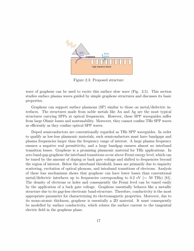
Figure 2.3: Proposed structure
wave of graphene can be used to excite this surface slow wave (Fig. 2.5). This sectionstudies surface plasma waves guided by simple graphene structures and discusses its basicproperties.
Graphene can support surface plasmons (SP) similar to those on metal/dielectric in-terfaces. The structures made from noble metals like Au and Ag are the most typicalstructures carrying SPPs at optical frequencies. However, these SPP waveguides sufferfrom large Ohmic losses and nontunability. Moreover, they cannot confine THz SPP wavesas efficiently as they confine optical SPP waves.
Doped semiconductors are conventionally regarded as THz SPP waveguides. In orderto qualify as low-loss plasmonic materials, such semiconductors must have bandgaps andplasma frequencies larger than the frequency range of interest. A large plasma frequencyensures a negative real permittivity, and a large bandgap ensures almost no interbandtransition losses. Graphene is a promising plasmonic material for THz applications. Inzero band-gap graphene the interband transitions occur above Fermi energy level, which canbe tuned by the amount of doping or back gate voltage and shifted to frequencies beyondthe region of interest. Below the interband threshold, losses are primarily due to impurityscattering, excitation of optical phonons, and intraband transitions of electrons. Analysisof these loss mechanisms shows that graphene can have lower losses than conventionalmetal/dielectric interfaces up to frequencies corresponding to 0.2 eV (∼ 50 THz) [81].The density of electrons or holes and consequently the Fermi level can be tuned easilyby the application of a back gate voltage. Graphene essentially behaves like a metallicstructure due to its gap-less electronic band-structure. Therefore, conductivity is the mostappropriate parameter for characterizing its electromagnetic properties. Moreover, due toits mono-atomic thickness, graphene is essentially a 2D material. It must consequentlybe modelled by surface conductivity, which relates the surface current to the tangentialelectric field in the graphene plane.
17

0 2 4 6 8
x 1013
0
0.2
0.4
0.6
0.8
1
X: 1.001e+013Y: 0.348
Ferm
i le
vel (e
v)
carrier density (cm−2
)
Figure 2.4: Fermi level versus surface carrier density
Different methods, mainly random phase approximation and Kubo method, for calcu-lating the dielectric constant and conductivity of graphene have been discussed in severalrecent works. [82–86]. Here we use the results obtained from the Kubo formula [84]. Forhigh frequencies, ω � kvf , τ
−1, the dynamical conductivity, σ = σ′ + jσ′′, can be writtenas:
σ(ω) =ie2kBT
π~2
1
ω − iΓ
(µckBT
+ 2 ln(e−µc/kBT + 1
))+
e2
4~
(G(ω)− i2ω
π
∫ ∞0
G(ω′)−G(ω)
ω2 − ω′2dω′)
G(ω) =sinh(~ω/2kBT )
cosh(µc/kBT ) + cosh(~ω/2kBT )
(2.7)
where µc is the chemical potential, Γ = 1/τ is a phenomenological scattering rate, T istemperature, kB is the Boltzmann constant, and e is the charge of an electron. There isno external magnetic field, and so the local conductivity is isotropic.
For an isolated graphene sheet, the chemical potential, µc, is determined by the carrier
18

Figure 2.5: The graphene SPP waveguide
density ns:
ns =2
π~2v2f
∫ ∞0
ε (f(ε− µc)− f(ε+ µc)) dε, (2.8)
in which f(ε) =(eε/kBT + 1
)−1is the Fermi-Dirac distribution and vf ∼= 106 m/s is
the Fermi velocity. The carrier density can be controlled via chemical doping or electricalgating. The plot of chemical potential versus carrier density obtained from eq. 2.8 is shownin Fig. 2.4.
The first term in Eq.2.7 corresponds to the intraband electron-photon scattering pro-cesses, and is similar to the Boltzmann-Drude expression. The second term in Eq.2.7corresponds to the direct interband electron transitions. The interband transition occursabove the frequency threshold ~ω ≈ 2µc.
The structure under consideration is shown in Fig. 2.5. The propagation direction isalong z, and the structures are assumed to be infinite and invariant along the y axis.
Since the structure is two dimensional, we have TE and TM modes. The field distri-bution for the TM mode is:{
(Ex1, Ez1, Hy1)e−α0xe−jβzz x > 0
(Ex2, Ez2, Hy2)eαSixe−jβzz x < 0(2.9)
where α0 =√β2z − k2
0 and αSi =√β2z − εSik2
0. The TE mode has a similar field distribu-tion for its Hz, Hx and Ey field components. The dispersion equation for the propagationconstant of each mode is obtained from the solution of Maxwell’s equations in each mediumand the following boundary conditions at the graphene interface.
n× (H1 −H2) = σEt (2.10)
19

10-3 10-2 10-1 100 101
f (THz)
-0.2
-0.1
0
0.1
0.2
0.3
0.4 &
(
S)
c=0.3eV =10 10-12s
c=0.3eV =10 10-12s
c=0.1eV =10 10-12s
c=0.1eV =10 10-12s
c=0.1eV =3 10-12s
c=0.1eV =3 10-12s
Figure 2.6: The real and imaginary parts of conductivity versus frequency for differentvalues of chemical potential and relaxation time.
The dispersion equation obtained for TE surface waves is:
α0
ωµ0
+αSiωµ0
= −jσ (2.11)
and for TM waves is:
ωε0α0
+ωεSiαSi
= jσ (2.12)
From the above two dispersion equations it is clear that the imaginary part of dynamicconductivity σ = σ′+jσ′′, determines which type of surface wave, TE or TM, can propagate.When σ′′ is positive, graphene guides the TE SPP wave, and when the σ′′ is negative,graphene behaves like a thin metal film capable of supporting TM SPP surface waves.
The sign of σ′′ depends on which of the internand and intraband terms in the conductiv-ity relation is dominant. The imaginary part of conductivity, corresponding to intraband
20

10-1 100
f (THz)
10
20
30
40
50
60
z/k0
substrate:Si c=0.1eV
substrate:SiO2
c=0.1eV
substrate:Si c=0.3eV
substrate:SiO2
c=0.3eV
(a) propagation constant
10-1 100
f (THz)
10-2
10-1
z/k0
substrate:Si c=0.1eV
substrate:SiO2
c=0.1eV
substrate:Si c=0.3eV
substrate:SiO2
c=0.3eV
(b) attenuation constant
Figure 2.7: Normalized (a) propagation constant and (b) attenuation constant of TM wavecarried by graphene layer on top of Si and SiO2 substrate. The solid and dotted lines areplotted for graphene chemical potention 0.1 eV and 0.3 respectively. The τ = 10× 10−12sfor all curves.
transitions, is negative, but is positive for the conductivity, corresponding to interbandtransitions. In graphene with non-zero Fermi energy, the Boltzmann-Drude intrabandterm is dominant in the THz frequency range when ~ω/2 < |µ|. On the other hand, theinterband term is dominant at higher frequencies when |µ| < ~ω/2. Therefore, for Fermienergies greater than 0.2 meV, graphene can support TM SPP waves at the THz frequencyrange. Figure 2.6 shows the real and imaginary parts of the conductivity for different valuesof Fermi level versus frequency.
2.5.1 Two-layer structure
The simplest graphene based SPP waveguide is a graphene layer on top of a Si or SiO2
substrates. The relative dielectric constants of Si and SiO2 at THz range of frequency areεsi = 11.7 − j0.0014 and εsio2 = 3.84 − j0.0314, obtained from experimental values [87].The propagation and attenuation constants of TM plasmonic waves obtained by solvingequation 2.12 are depicted in Figure 2.7 for two values of chemical potential. The largepropagation constant of 50k0 is obtained for an SPP wave of graphene on a silicon substratefor µc = 0 eV and τ = 10× 10−12 s at 1 THz. The propagation constants of slow waves of
21

0 0.05 0.1 0.15 0.2 0.25 0.3
c (eV)
0
20
40
60
z/k0
substrate:Sisubstrate:SiO
2
(a) propagation constant
0 0.05 0.1 0.15 0.2 0.25 0.3
c (eV)
0
0.2
0.4
0.6
0.8
1
z/k0
substrate:Sisubstrate:SiO
2
(b) attenuation constant
Figure 2.8: Normalized (a) propagation constant and (b) attenuation constant of TM waveversus chemical potentioal of the graphene layer for τ = 10µs at f=1 THz. The blue andred curves are for TM wave carried by graphene layer on top of Si and SiO2 substraterespectively.
the grating structures are big. Therefore, SPP waves can be used to excite these waves.
The attenuation constant of the SPP wave is determined by two factors: the grapheneloss and the substrate loss. When the SPP wave is more confined to the graphene layer, thegraphene loss plays the dominant role, and when it is less confined to the graphene layerand more spread out, the loss of the substrate plays the dominant rule. The normalizedpropagation constant and thus the confinement of the electromagnetic field to the graphenelayer is higher at larger frequencies. The refractive index of Si is higher than that ofSiO2. Therefore, on the Si substrate, the field is more confined to the graphene layerand the attenuation constant is higher. However, for µc = 0.3ev, at frequencies lowerthan f ≈ 0.07THz the attenuation constant for the SiO2 substrate is higher. At thesefrequencies, the field is less confined to the graphene layer and penetrates more into thesubstrate. Therefore, the loss of the substrate playes the dominant role, and since SiO2
has higher intrinsic loss than Si, the attenuation constant for the SiO2 substrate is higher.
Figure 2.8 shows that the normalized propagation constant and attenuation constantdecrease by increasing the chemical potential. Increasing the chemical potential of thegraphene increases σ′ and |σ′′| (see Fig. 2.6). Moreover, it can be seen in eq. 2.12, thatincreasing |σ′′| decreases the real part of α0,si, resulting in an increase of the real part of
the propagation constant (αSi,0 =√β2z − εSi,0k2
0). Thus, for larger chemical potential, thefield propagates with the lower phase velocity and is more confined to the graphene layer.Since graphene is a lossy medium, more confinement to the graphene layer, results in a
22

0 0.02 0.04 0.06 0.08 0.1−0.01
−0.005
0
0.005
0.01
x/λ
z/λ
real(Hy)/max(real(H
y))
−0.8
−0.6
−0.4
−0.2
0
0.2
0.4
0.6
0.8
air
Si
f=1THz µc=0 τ=3×10
−12
Graphene
(a) Re(Hy)
0 0.02 0.04 0.06 0.08 0.1−0.01
−0.005
0
0.005
0.01
x/λ
z/λ
real(Ez)/max(real(E
z))
−0.8
−0.6
−0.4
−0.2
0
0.2
0.4
0.6
0.8f=1THz µ
c=0 τ=3×10
−12
air
Si
Graphene
(b) Re(Ez)
0 0.02 0.04 0.06 0.08 0.1−0.01
−0.005
0
0.005
0.01
x/λ
z/λ
real(Ex)/max(real(E
x))
−0.8
−0.6
−0.4
−0.2
0
0.2
0.4
0.6
0.8
1
air
Si
f=1THz µc=0 τ=3×10
−12
Graphene
(c) Re(Ex)
0 0.02 0.04 0.06 0.08 0.1−0.01
−0.005
0
0.005
0.01
x/λ
z/λ
real(Pex
/max(Re(P))
0
0.01
0.02
0.03
0.04
0.05f=1THz µ
c=0 τ=3×10
−12
air
Graphene
Si
(d) Re(Px)
0 0.02 0.04 0.06 0.08 0.1−0.01
−0.005
0
0.005
0.01
x/λ
z/λ
real(Pez
)/max(Re(P))
0.1
0.2
0.3
0.4
0.5
0.6
0.7
0.8
0.9f=1THz µc=0 τ=3×10
−12
air
Si
Graphene
(e) Re(Pz)
Figure 2.9: The profile of normalized real part of (a)Re(Hy) (b)Re(Ez) (c)Re(Ex)(d)Re(Pex) (e)Re(Pez) in the xz plane at f=1THz for µc=0ev and τ=3× 10⁻¹².
larger attenuation constant. The carrier density and thus the chemical potential can becontrolled easily by a gate voltage.
The normalized real part of non-zero components of the TM surface field in an xz plane,where z aligns with the propagation direction, is depicted in Fig. 2.9. It is assumed thatthe graphene strip is wide enough to neglect the variation of the field along the y axis farfrom the edges. These figures show the surface nature of SPP-waves and the capabilityof graphene to effectively suppress the magnetic field and prevent it penetrating to thetop layer with a lower refractive index. These results show that, despite being just oneatom layer thick, graphene acts like a good conductor, shielding the magnetic field. Thetransverse component of the electric field has a symmetric profile, and the perpendicularcomponent has an antisymmetric profile. As a general rule, there is a trade off betweena larger propagation distance and stronger confinement. We show the tunability of prop-
23
agation and attenuation constants via electrical gating. This feature can be exploited inrealization of phase delays or modulators based on a monolayer of graphene.
24

Chapter 3
Quantum mechanical analysis oftravelling wave amplification ingraphene
In this chapter, a quantum mechanical method is developed to analyze the travelling waveamplification in graphene. First a qualitative description of the gain mechanism and gainconditions is presented. Then quantitative analysis is presented by calculating the conduc-tivity of graphene.
In the previous chapter, the graphene conductivity obtained from Kubo formula [74]was presented (eq. 2.7) This expresion is given for a small spatial dispersion, kvf << ~ω,under local equilibrium condition. Neither of these assumptions is applicable for travellingwave amplification conditions in graphene. In TWAs, the charged carriers are biased tohave a drift velocity, and the electromagnetic waves are slowed down to have a phasevelocity smaller than the drift velocity of carriers. For graphene with drifting carriers,the equilibrium condition is not applicable. Also for very slow electromagnetic waves, thewavenumber, k = 2π/Vph, cannot be assumed to be negligible any more. Therefore, in thischapter, the conductivity of graphene for drifting charge carriers is obtained by applyingthe drifting Fermi distribution function to the conductivity response function of graphene.The frequency and wavenumber dependent conductivity of graphene is obtained for driftingcharge carriers as a function of chemical potential and drift velocity.
The travelling wave interaction can be described as a stimulated intraband radiativetransition of electrons. In contrast to the mechanism of radiation in lasers, wherein the elec-trons transit from the conduction to the valence band to emit photons. In travelling wave
25

Figure 3.1: (a) Direct interband radiative transition, (b) indirect intraband transition
amplifiers, the radiative intraband transitions play the dominant role in electromagneticamplification. Amplification can be achieved when there is a large electron population atthe higher energy states. In travelling wave amplifiers, this population inversion is achievedby applying a drift DC current and increasing the average momentum of the electrons.
During transitions, three waves interact: the electron wave function in the both initialand final states, and the electromagnetic wave. The energy and momentum should beconserved during the transition. Considering an electromagnetic wave with a frequency ofω and wavevector of q, in a radiative transition, we should have
Ei − Ef = ~ω (3.1)
ki − kf = q (3.2)
where Ei and Ef are the energy of the electron states at the initial and final states respec-tively; ω and q are the frequency and wave number of the electromagnetic wave, and kiand kf are the electron wave numbers of the initial and final states, respectively.
Figure 3.1 shows that if the transition occurs in a vacuum or in a homogeneous medium,the two conditions of 3.1 and 3.2 can be satisfied simultaneously only for interband tran-sitions. However, for intraband transition, the wavenumber of the electromagnetic waveshould be increased to a value greater than ω/Vf . This increase can be achieved in a peri-odic structure where one of the space harmonics has a large enough propagation constantto balance the momentum equation 3.2.
Figure 3.2 illustrates schematically how the population inversion is induced in travellingwave amplifiers. In this figure, the picture on the right is the top view of the left one. In a
26

Figure 3.2: Schematic demonstration of population inversion in graphene by increasing theaverage momentum of electrons. The blue and orange circles are the Fermi circles of filledstates in k-space of an unbiased and biased graphene, respectivly at T=0. The green andred curves denote, respectively, the lower and upper energy states in k-space that satisfyboth energy and momentum conservation equations (eq. 3.1 and 3.2).
travelling wave amplifier, instead of injecting carriers electrically or optically, the electronsare accelerated to a high drift velocity, equivalent to increasing the average momentum ofelectrons in the solid. Therefore, the whole electron density distribution will be shifted inthe k-space by the value of kd, which is a function of the drift velocity of electrons, Vd.
Figure 3.2(b) shows schematically how increasing the value of kd will eventually leadto population inversion. In this figure, it is assumed that the temperature, T , is zero. Thestates inside the circle with the radius of kf = Ef/~Vf are full, and the states outside ofthis circle are empty. The density of electrons is not changed in a moving frame. Therefore,the radius of the Fermi circle remains constant. The red and green curves denote the statesin k-space that satisfy both equations 3.1 and 3.2. As shown in Fig. 3.2, by increasingthe value of kd, more higher-energy states (red curve) are filled and, simultaneously, lowerenergy states (green curve) are emptied until, for a sufficiently large value of Vd, the lengthof the red curve covered by the Fermi circle becomes greater than that for the green one.In this case, the population inversion has occurred, and a net gain is achieved.
27

The above discussion has only described qualitatively the gain mechanism in travel-ling wave amplifiers. We next apply linear response theory to drive the conductivity ofgraphene.
The Hamiltonian equation of a system with a small perturbation can be written asin [88]
H(t) = H0 + F (t)B (3.3)
where H0 is a time-independent diagonal matrix, and F (t) is the external time-dependentfield that couples linearly to an observable B. F (t) is assumed to be a small time dependentperturbation expressed as ei(ω−iδ)t. Then, the perturbation of an observable A (A(t) =A0 + A1e
i(ω−iδ)t) is
〈A1〉(ω) = χAB(ω)F (ω) (3.4)
where χAB(ω) is the linear response function of the system and defined as [88]
χAB(ω) =∑mn
fm − fn~ω + En − Em − i~δ
BmnAnm (3.5)
A complete discussion and derivation of the linear response function is given in [88].The Hamiltonian of Dirac electrons in the presence of an electromagnetic field is
H = H0 + J ·A(r, t) (3.6)
where A(r, t) = A0ei(ωt−βz) is the vector potential, and J is the current operator. By
comparing this Hamiltonian (eq. 3.6) with the general form of the Hamiltonian of asystem under perturbation (eq. 3.3), the current induced by the external vector potentialis obtained as
J(ω,q) = χJJ(ω,q)A(ω,q), (3.7)
where χJJ, a 2 × 2 matrix, is the current-current response function of the graphene. Thecurrent operator of graphene is [89]
J = evf σ (3.8)
in which σ is the Pauli matrices vector. Therefore, the current-current response functionelement can be written as
28

Figure 3.3: Graphene sheet; lying in the y-z plane, illuminated with a TMz electromagneticfield
χJαJβ
(q, ω) = gsgve2v2f
∑ss′
∑k
λαβss′(k,q)f(Ek,s)− f(Ek+q,s′)
Ek+q,s′ − Ek,s + ~(ω − iδ)(3.9)
whereλαβss′(k,q) = 〈k, s|σα|k + q, s′〉〈k + q, s′|σβ|k, s〉 (3.10)
is the overlap of states which includes particular chirality properties of graphene. In eq. 3.9,gs = gv = 2 denotes the spin and valley degeneracy, and f(Ek,s) is the Fermi distributionfunction. The energy dispersion relation of graphene is Ek,s = s~vf |k|. χ
JαJβis the
response function of the current in the α direction induced by a vector potential in the βdirection. For a graphene layer in the yz plane α, β = z, y and the σz and σy equal σ1 andσ2 respectively, where σ1 = ( 0 1
1 0 ) and σ2 =(
0 −jj 0
)are the Pauli matrices.
In equations 3.9 and 3.10, the terms for s = s′ = ±1 represent the electron-electron(s = 1) and hole-hole (s = −1) intraband transitions, and the s 6= s′ represent the interbandtransitions. In equation 3.10, |ks〉 are the electron and hole wave vectors that diagonalizethe independent electron Hamiltonian, H0, of graphene.
|k, s〉 =1√2
(e−iθk
±e−iθk
)eik·r. (3.11)
We assume that a TMz electromagnetic field illuminates the graphene sheet lying inthe y-z plane (see Fig. 3.3). Therefore, the vector potential and the electric field in theplane of graphene are in the z-direction. We are interested exclusively in the longitudinalz-component of the induced current, which is the only component that can be coupled tothe incident electromagnetic field. By substituting eq. 3.11 in eq. 3.10 for λzzss′ , we obtain
29

1000 2000 3000 4000 5000/k
0
-1
-0.5
0
0.5
1
1.5
2
Rea
l()
(S)
10-4
Vd=0 m/s
Vd=3 105 m/s
200 400 600 800 1000/k
0
-0.03
-0.02
-0.01
0
0.01
0.02
Imag
()
(S)
Vd=0 m/s
Vd=3 105 m/s
Figure 3.4: Real and imaginary parts of the conductivity versus β at f = 1 THz forµc = 0.3 eV and two values Vd = 0 m/s(dotted line) and Vd = 3× 10⁵ m/s (solid line).
λzzss′(k,q) =1 + ss′ cos(θk + θk+q)
2
=1
2+ss′
2
(k cos(2θk) + q cos(2θk) cos(θk)√
k2 + q2 + 2kq cos(θk)+
q sin(θk)sin(2θk)√k2 + q2 + 2kq cos(θk)
) (3.12)
where k = |k|, and θk is the angle of k from z axis. To obtain the second expression, thewavevector q is assumed to be in the z direction, θq = 0.
To analyze the response of drifting carriers, the Fermi distribution function of electronswith the average drift velocity of Vd is substituted in eq. 3.9, which is [90]
f(Ek,s) =1
1 + e((Ek,s−P·Vd−µc)/kBT)(3.13)
To calculate eq. 3.9 numerically, the summation over k,∑
k, is replaced by 2D inte-
gration∫ ∫ |k|
(2π)2dθkdk using 2D density of states in the k-space. The second expression
in eq.3.12, which gives λzzss′ explicitly as a function of θk and |k|, is used to numericallycalculate the 2D integral in the cylindrical coordinate system.
The conductivity of graphene is σzz = iχJzJz
/ω (Jz = σzzEz and E = −iωA). The realpart of the conductivity shows whether we have gain or loss. The real part of conductivityis positive for lossy materials and negative for materials with gain.
30

0.5 1 1.5 2 2.5 3 3.5 4 4.5 5−1
0
1
2x 10
−4
Vd/V
ph
Real(
σ)
(S)
Vd = 3× 10
5 (m/s)
τ=10 × 10−12
(s)
uc=0.3 ev
f=1 THzf=500 GHzf=300 GHz
0.5 1 1.5 2 2.5 3 3.5 4 4.5 5−5
0
5
10
15x 10
−5
Vd/V
ph
Real(
σ)
(S)
Vd = 3× 10
5 (m/s)
τ=10 × 10−12
(s)
f=1 THz
uc=0.2 ev
uc=0.3 ev
0.5 1 1.5 2 2.5 3 3.5 4 4.5 5−5
0
5
10
15x 10
−5
Vd/V
ph
Real(
σ)
(S)
f=1 THz
τ=10 × 10−12
(s)
uc=0.3 ev
Vd=1 × 10
5 (m/s)
Vd=2 × 10
5 (m/s)
Vd=3 × 10
5 (m/s)
0.5 1 1.5 2 2.5 3 3.5 4 4.5 5−1
−0.5
0
0.5
1
1.5x 10
−4
Vd/V
ph
Real(
σ)
(S)
Vd = 3× 10
5 (m/s)
f=1 THz
uc=0.3 ev
τ=10 × 10−12
(s)
τ=100 × 10−12
(s)
Figure 3.5: Real part of conductivity versus Vd/Vph for different values of the frequencygiven Vd = 3× 10⁵ m/s, τ = 10−11 and uc = 0.3 eV (top left); the chemical potential givenVd = 3× 10⁵ m/s and τ = 10−11 s at the frequency of 1THz (top right); the drift velocitygiven uc = 0.3 eV and τ = 10−11 s at the frequency of 1THz (bottom left); and the collisionrelaxation time given Vd = 3× 10⁵ m/s and uc = 0.3 eV (bottom right).
In Fig. 3.4, the real and imaginary parts of the conductivity versus β = q are plottedat f = 1 THz for µc = 0.3 eV, τ = 10 × 10−12 s, and two values: Vd = 0 (dottedline) and Vd = 3 × 10⁵ m/s (solid line). The real part of the conductivity is negative forVd = 3 × 10⁵ m/s and for β > 1112k0 which corresponds to Vph < 0.9Vd (β = ω/Vph).Here, the calculated conductivity also confirms that in order to have gain, a drift velocityshould be applied and the electromagnetic wave should be slowed down to phase velocitiessmaller than the drift velocity of electrons.
In the previous chapter it was shown that the imaginary part of the graphene conduc-tivity for β ≈ 0 and Vd = 0, is negative (Fig. 2.6). Consistent with this result, in Fig.3.4(b), the imaginary part of the conductivity is also negative for small values of β < 320k0
and both Vd = 0 and Vd = 3× 10⁵ m/s.
In the proposed TWA, graphene acts as a current source. Therefore, the real part of
31

−0.2 −0.1 0 0.1 0.2 0.3−5
−4
−3
−2
−1
0
1x 10
−5
uc (ev)
Re
al(
σ)
(S)
Vd = 3× 10
5
τ=10µs
f=1 THz
intraband conduction transition
intraband valence transition
conduction−valence transition
valence−conduction transition
Figure 3.6: The real part of four different interband and intraband conductivity termsversus chemical potential
the conductivity is more important for the analysis (see Chapter 5). The effect of theimaginary part of the conductivity is to change the real part of the dielectric constant.Since graphene is a zero thickness conductor, this effect is insignificant.
in Fig. 3.5 a-d, the real part of the conductivity is plotted versus Vd/Vph for differ-ent values of frequency, chemical potential, drift velocity, and collision relaxation time(τ = 1/δ). The maximum negative conductivity is increased by increasing the chemicalpotential or equivalently electron density, and the drift velocity. Figure 3.5(a) shows thatthe electromagnetic wave should be slowed down more for higher frequencies to achievethe maximum gain.
In Figure 3.6 the four different interband and intraband conductivity terms versuschemical potential are plotted separately to show the contribution of each individually(eq. 3.9). This figure shows that, for a positive chemical potential, the radiative electron-electron intaraband transitions in the conduction band cause amplification (s=s’=+1),and for a negative chemical potential, the hole-hole transitions in the valence band arethe source of amplification. Except for chemical potential values close to zero, the effectof interband transitions are negligible with respect to the intraband terms. As expected,the transitions from valence band to conduction band, during which a photon is absorbed,gives positive conductivity, and the transition from conduction to valence band involvingphoton emission gives negative conductivity.
32

3.1 Conclusion
In this chapter, the travelling wave amplification in graphene is explored both qualitativelyand quantitatively. The quantum mechanical approach is applied to obtain the frequencyand wave number dependent conductivity of graphene with drifting charge carriers under anon-equilibrium condition. The conductivity relations show that for a slow electromagneticfield with the phase velocity smaller than the drift velocity of carriers, graphene changesfrom a lossy propagating medium to a gain medium that converts power from the DCsource to the electromagnetic field. This result shows that graphene can be used in solidstate travelling wave amplifiers.
The quantum mechanical approach gives significant insight into the physical mechanismof traveling wave interactions inside graphene. It is a very precise model for an idealsystem with no defects and disorder and for small source perturbation. However, it isextremely hard to model all macroscopic phenomena, quantum mechanically. Therefore, inthe next chapter, a more classical approach based on the hydrodynamic model of grapheneis presented.
33

Chapter 4
Hydrodynamic model of graphene
It is reasonable to use a hydrodynamic approach to describe the dense electron-hole plasmain semiconductor systems in which the electron-electron, electron-hole, and hole-hole col-lisions predominate over collisions between electrons and holes with disorder. These colli-sions can occur in intrinsic graphene at room temperature, in gated graphene at sufficientlyhigh gate voltages, and in graphene under strong optical pumping. Hydrodynamic modelsof electron-hole systems in semiconductors with parabolic energy spectra of electrons andholes are widely used. However, for graphene, such models need to be revised due to the lin-ear energy spectra of electrons and holes. The hydrodynamic model of graphene was usedto describe the stationary transport processes in graphene [91]. It was also used to analyzeelectron (or hole) plasma waves in gated graphene in a state in which the Fermi level wasfar from the Dirac point and quasi-neutral electron-hole sound waves in bipolar electron-hole plasma [92]. Based on this model, the DC conductivity and frequency dependent acconductivity of graphene were calculated [93,94]. In this chapter, the hydrodynamic modelis used for the first time to obtain the frequency and wave number dependent conductivityof the harmonic perturbation of moving charged carriers in graphene [95].
Electrons in graphene behave like a Dirac fluid of massless quasi-particles, propagatingat a Fermi speed of about vf ' 106m/s. Therefore, the electrons in graphene mimic zeromass relativistic particles with an effective light speed of vf = c/3000. The maximumdrift velocity of graphene is Vsat ∼ 105m/s [91]. Thus, to analyze graphene with driftingcarriers, the hydrodynamic description derived from a relativistic fluid approach can beused [75]. Since electron-phonon and electron-impurity scattering have a negligible impacton the linear response of graphene over substrate at room temperature, the analyzed modelis based only on electron-electron elastic scattering. Therefore, only the electron-electron
34
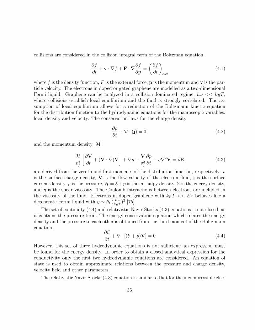
collisions are considered in the collision integral term of the Boltzman equation.
∂f
∂t+ v · ∇f + F · ∇∂f
∂p=
(∂f
∂t
)coll
(4.1)
where f is the density function, F is the external force, p is the momentum and v is the par-ticle velocity. The electrons in doped or gated graphene are modelled as a two-dimensionalFermi liquid. Graphene can be analyzed in a collision-dominated regime, ~ω << kBT ,where collisions establish local equilibrium and the fluid is strongly correlated. The as-sumption of local equilibrium allows for a reduction of the Boltzmann kinetic equationfor the distribution function to the hydrodynamic equations for the macroscopic variables:local density and velocity. The conservation laws for the charge density
∂ρ
∂t+∇ · (j) = 0, (4.2)
and the momentum density [94]
Hv2f
[∂V
∂t+ (V · ∇)V
]+∇p+
V
v2f
∂p
∂t− η∇2V = ρE (4.3)
are derived from the zeroth and first moments of the distribution function, respectively. ρis the surface charge density, V is the flow velocity of the electron fluid, j is the surfacecurrent density, p is the pressure, H = E+p is the enthalpy density, E is the energy density,and η is the shear viscosity. The Coulomb interactions between electrons are included inthe viscosity of the fluid. Electrons in doped graphene with kBT << EF behaves like adegenerate Fermi liquid with η ∼ ~ρ( EF
kBT)2 [75].
The set of continuity (4.4) and relativistic Navir-Stocks (4.3) equations is not closed, asit contains the pressure term. The energy conservation equation which relates the energydensity and the pressure to each other is obtained from the third moment of the Boltzmannequation.
∂E∂t
+∇ · [(E + p)V] = 0 (4.4)
However, this set of three hydrodynamic equations is not sufficient; an expression mustbe found for the energy density. In order to obtain a closed analytical expression for theconductivity only the first two hydrodynamic equations are considered. An equation ofstate is used to obtain approximate relations between the pressure and charge density,velocity field and other parameters.
The relativistic Navir-Stocks (4.3) equation is similar to that for the incompressible elec-
35

tron liquid in semiconductors [96], ρm∗e
[∂V
∂t+ (V · ∇)V
]+∇p− η∇2V = ρE, except for
an extra relativistic termV
v2f
∂p
∂t. m∗e is the effective electron mass of the semiconductor. For
massless electrons in graphene, this term is replaced by H/ρv2f which can be considered as
effective electron mass of graphene. The electrons in doped graphene act like a degenerateFermi gas. The pressure of degenerate Fermi gas can be written as
p = p0 +O(
(kBT
EF
)2
) (4.5)
where p0 is the electron degeneracy pressure at zero temperature. Since in our applica-tion we are mainly interested in the high density of electrons and thus high Fermi energies(kBT << EF ), the pressure is approximated with its value at zero temperature. Withthe aid of thermodynamic relation U = TS + pV and employing the condition T = 0, thepressure can be obtained from this equation of state [97]
p = −(∂U0
∂A
)N
(4.6)
where the subscript N is the total number of charged particles, which is assumed to re-main constant during the process, A is the area of the graphene and U0 is the internal energyat T = 0. This assumption is valid when the power of electromagnetic wave is not high in away that the system remains in equilibrium (or so-called quasi-equilibrium). The internalenergy is the mean value of the total energy of the system given by U = A
∫Eg(E)f(E)dE,
where f(E) is the Fermi-Dirac distribution function and g(E) = gsgv|E|/(2π(~vf )2) is theenergy density of states in graphene. Here, the spin and valley degeneracy are accountedby gs = gv = 2. For graphene 2DEG with linear band dispersion equation (4.6) for thepressure yields [93]
p =1
3
√π~vfρ2/3(r, t) =
1
3EFρ(r, t). (4.7)
where the Fermi energy of the graphene is EF = ~vf√πρ.
To find the conductivity of graphene as a function of frequency, ω, and propagationconstant, β, an infinite graphene sheet lying in the y-z plane illuminated with a TMz
electromagnetic field is assumed, with a propagation constant of β in the z direction (Fig.3.3), E = (Ex, Ez)e
iωte−iβz. To obtain the conductivity, it is necessary to first find the
36

induced current density in the linear response regime, which in this case has only the zcomponent. The longitudinal conductivity can then be defined using Ohm’s law jz = σEz(σ = σzz).
The charge and velocity of the graphene electron fluid can be written as
ρ = ρ0 + δρei(ωt−βz) (4.8)
andV = Vd + δVei(ωt−βz). (4.9)
Here, ρ0 is the electron charge density at equilibrium, δρei(ωt−βz) is the induced chargedensity, Vd is the drift velocity applied by a DC voltage (assumed to be in the z direction),and δVei(ωt−βz) is the induced velocity. From this point on, the phasor form of time-space-varying variables is used to suppress the ei(ωt−βz) term.
The linear response of the system to a small electromagnetic field perturbation is de-termined by considering only the first-order terms in equations 4.4 and 4.3. The inducedcurrent is
j = ρ0δV + δρVd. (4.10)
For the pressure gradient in Eq. 4.3,
∇p =∂p
∂ρ∇δρ ≈ 1
2EF (ρ0)(−iβδρz) (4.11)
where the approximation in the second equation consists of only the first-order term andassumes the Fermi energy to be effectively time and position independent. The relativisticcorrection term is found through
V
v2f
∂p
∂t=
Vd
v2f
1
2EF (ρ0)(iωδρ). (4.12)
For small drift velocities at low frequency, this term can be neglected, and the non-relativistic Navier-Stokes hydrodynamics equation is recovered. The enthalpy density H =E + p equals
H =3
2
∫ ∞0
g(E)
(E
e(E−EF )/kBT + 1+
E
e(E+EF )/kBT + 1
)dE (4.13)
37

1000 2000 3000 4000 5000/k
0
-1
-0.5
0
0.5
1
1.5
2
Rea
l()
(S)
10-3
Vd=0 m/s
Vd=3 105 m/s
200 400 600 800 1000
/k0
-8
-6
-4
-2
0
2
Imag
()
(S)
10-3
Vd=0 m/s
Vd=3 105 m/s
Figure 4.1: Real and imaginary parts of the conductivity versus β at f = 1 THz forµc = 0.3 eV and two values Vd = 0 m/s(dotted line) and Vd = 3× 10⁵ m/s (solid line).
in which g(E) = gsgv/(2π(~vf )2) is the energy density of states. Here, the spin andvalley degeneracy are accounted for by gs = gv = 2. The Fermi energy in this equationis assumed to be constant in time and space. The prefactor 3/2 comes from the p = E/2relation. At high values of chemical potential, the H value (Eq. 4.13) is close to its valueat T = 0, ρEF , which satisfies the Gibbs-Duhem relation. For example for EF = 0.3 eV atT = 300 k, H/ρEF = 0.95. By substituting equations 4.10, 4.11 and 4.12 into equations4.4 and 4.3, it is found that
σ(ω, β) =
β2ηe2
m2effω
2A− j ρ0e2
meffω
(A2 + βVd
4ω− β2Ef
2meffω2
)(A2 + βVd
3ω− β2Ef
2meffω2
)2
+(
ηβ2
meffωρ0A)2 (4.14)
in which A = 1− βVd/ω and meff = EF (ρ0)/v2f . The conductivity of graphene for Vd = 0
is
σ(ω, β, Vd = 0) =
β2ηe2
m2effω
2 − j ρ0e2
meffω
(1− β2Ef
2meffω2
)(
1− β2Ef2meffω2
)2
+(
ηβ2
meffωρ0
)2 (4.15)
As expected the non-biased graphene (Vd = 0) is always lossy for all frequencies andphase velocities.
In Fig. 4.1, the real and imaginary parts of the conductivity versus β are plotted atf = 1 THz for µc = 0.3 eV and two values: Vd = 0 (dotted line) and Vd = 3 × 10⁵ m/s
38

0.5 1 1.5 2 2.5 3 3.5 4 4.5 5
Vd/V
ph
-1
0
1
2
Re
al(
) (S
)
10-4
Vd=10
5 m/s
f=1 THz
f=500 GHz
f=300 GHz
f=100 GHz
0.5 1 1.5 2 2.5 3 3.5 4 4.5 5
Vd/V
ph
0
0.5
1
1.5
2
imag(
) (S
)
10-3
Vd=10
5 m/s
f=1 THz
f=500 GHz
f=300 GHz
f=100 GHz
Figure 4.2: Real and imaginary parts of conductivity versus Vd/Vph at frequencies of 0.1,0.3, 0.5 and 1 THz for a drift velocity of Vd = 105m/s.
(solid line). The result of this figure can be compared with the similar result of Fig. 3.4obtained from quantum mechanical model. remarkable similarity excits between these tworesults. Here again, it can be seen that the real part of the conductivity is negative forVd = 3 × 10⁵ m/s and for β > 1000k0 which corresponds to Vph < Vd. As expected, thenon-biased graphene is always lossy for every value of frequency and wavenumber. Also,the imaginary part of the conductivity is negative only for small values of β (β < 380k0
for Vd = 0 and β < 440k0 for Vd = 3× 10⁵ m/s).
The real and imaginary parts of the conductivity versus the normalized reciprocal valueof the phase velocity at different values of frequency are plotted in Fig. 4.2(a) and (b).The phase velocity is normalized to a drift velocity of Vd = 105m/s. The results showthat in biased graphene (Vd 6= 0) for β/βe > 1, or equivalently, for a drift velocity largerthan the phase velocity, Vd/Vph > 1, graphene changes from a lossy propagating mediumwith a positive real part of conductivity to a gain medium with a negative real part ofconductivity. In this case, the power transfers from the DC power to the electromagneticfield.
The real and imaginary parts of the conductivity versus frequency for different values ofdrift velocity are plotted in Fig. 4.3 where Ef = 0.3 eV. The wavenumber for all curves isβ = 2π/d, d = 100nm. This is consistent with the wavenumber of the first-order harmonicof a periodic structure with the period of d = 100nm. In the proposed graphene travellingwave amplifier, a periodic grating structure is used to generate a slow electromagnetic
39

wave. The propagation constant of the first-order harmonic of this structure is β1(ω) =β0(ω) + 2π/d, in which β0(ω) is the frequency-dependent propagation constant of thefundamental wave. The d values of the periodic slow wave structure should be in the rangeof few hundreds of nanometres or less to meet the amplification requirement of a graphenetravelling wave amplifier. In this range of d values, it is a sufficient approximation toconsider β1 ' 2π/d to be frequency independent.
The results displayed in Fig. 4.3 shows that the amount of gain and the frequencyrange at which amplification is possible are increased significantly by increasing the valueof the drift velocity.
In Fig. 4.3, the real and imaginary parts of the conductivity are plotted versus thefrequency for different values of Fermi energy, with β = 2π/(d = 100nm) and Vd = 105m/s.Raising the Fermi energy level leads an increase in the absolute value of the negativeconductivity and gain. However, as the Fermi energy increases, the frequency range atwhich the real part of the conductivity is negative (making amplification possible) doesnot change. An increase in the Fermi energy leads to an increase in the density of electrons,enhancing the transfer of energy from the electrons to the electromagnetic field. Since theexact value of viscosity, η, is not accurately known in the proposed analytical model, typicalvalues have been used in the conductivity equations. The effect on conductivity of changingthe viscosity from half to twice its typical value is depicted in Fig. 4.5. Changes in η alterthe bandwidth and gain simultaneously.
4.1 Conclusion
In this chapter, a hydrodynamic model, derived from a relativistic fluid approach, wasused to find the current induced by a harmonic perturbation of drifting charge carriersin graphene. The induced charge density and velocity were assumed to be significantlysmaller than the total charge density and the drift velocity applied by the DC bias toobtain the conductivity in the linear region.
The obtained results are consistent with the results of the previous chapter. Bothmethods show that the negative conductivity and thus gain is obtained for drift velocitiesslightly greater than the phase velocity of the incident field. Although the two methodsare quite different, one being more classical and the other more quantum mechanical, thebehaviour of the two conductivity functions with respect to the frequency and wavenumberare remarkably similar.
40

0 1 2 3 4 5
−1
−0.5
0
0.5
1
1.5
x 10−4
real(
σ)
(S)
f (THz)
d=100nm
Vd=0.5× 10
5
Vd=1× 10
5
Vd=2× 10
5
0 1 2 3 4 5
f (THz)
0
0.5
1
1.5
2
2.5
3
imag(
) (S
)
10-4
Vd=0.5 105
Vd=1 105
Vd=2 105
Figure 4.3: Real and imaginary parts of conductivity versus frequency for drift velocitiesof Vd = 0.5, 1, 2× 10⁵m/s where Ef = 0.3 eV. The propagation constant is assumed to befrequency independent and equals β = 2π/d, d = 100nm for all curves .
0 0.5 1 1.5
f (THz)
-1
-0.5
0
0.5
1
1.5
2
rea
l()
(S)
10-4
d=100nm, Vd=10
5m/s
Ef=0.1 ev
Ef=0.2 ev
Ef=0.3 ev
Ef=0.4 ev
0 0.5 1 1.5 2
f (THz)
0
1
2
3
4
5
imag(
) (S
)
10-4
Ef=0.1 ev
Ef=0.2 ev
Ef=0.3 ev
Ef=0.4 ev
Figure 4.4: Real and imaginary parts of conductivity versus frequency for different valuesof Fermi energy where Vd = 105m/s and β = 2π/d, d = 100nm.
41
0 0.5 1 1.5
−6
−4
−2
0
2
4
6
8
10x 10
−5
rea
l(σ
) (S
)
f (THz)
d=100nm, Vd=10
5m/s
0.5η
η
2η
0 0.5 1 1.5 20
0.2
0.4
0.6
0.8
1
1.2
1.4x 10
−4
imag(σ
) (S
)
f (THz)
λ=100nm, Vd=10
5m/s
0.5η
η
2η
Figure 4.5: Real and imaginary parts of conductivity versus frequency for different valuesof viscosity where Vd = 105 m/s, Ef = 0.3 eV and β = 2π/d, d = 100nm.
42

Chapter 5
Analysis of travelling-wave amplifierusing graphene
The quantum mechanical and hydrodynamic analysis of graphene that were presented inthe previous chapters show that travelling-wave amplification is possible in graphene. Thenext step is to design a structure to demonstrate and apply this fascinating property ofgraphene. Under certain conditions, when the charged particles in graphene move at ahigher velocity than an electromagnetic wave, energy transfers from the charged particlesto the electromagnetic field. The maximum drift velocity in the graphene is in the orderof 105m/s. The higher order space harmonics of a periodic waveguide can reach this levelof phase velocity. The ability to fabricate dielectric waveguides with very short periodgrating make it possible to use low-velocity charged-particle currents like drifting carriersin graphene.
In this chapter, a slow-waveguide structure is proposed in which the graphene layeris placed right next to the periodic layer; hence, capitalizing on the maximum couplingbetween the electromagnetic field and the drifting space charge wave in graphene (Fig.5.1). The waveguide is fabricated from high-resistivity silicon; such silicon having very lowloss at the THz range of frequencies [98,99].
An approximate analytic solution is presented for electromagnetic wave propagation in aperiodic structure in the presence of graphene. The analytic approximate expressions showthe effect of each parameter individually on the overall gain of the structure. Therefore, thisapproach provides insights for designing and optimizing the structure. Such transparencyis not achievable when using numerical calculations.
Below, the electromagnetic wave propagation in both a slab and a rectangular waveg-
43

Figure 5.1: Proposed structure is a high-resistivity silicon waveguide with a grating etchedon its top surface covered by a graphene sheet onto which metal contacts are attached
uide with a grating on the top surface is analyzed in terms of a Floquet mode solution.This method has been described by Gover and Yariv in [73,100]. First-order approximaterecursive analytical expressions for the space harmonics are obtained. The calculationin [73] was presented only for slab waveguides and the grating structure was modelled by asemi-infinite inhomogeneous layer. Therefore, the finite corrugation depth was not consid-ered in the calculations. Here, the aforementioned method is generalized to a three-layerstructures to model the effect of the grating depth accurately. A more generalized methodis then used to analyze rectangular waveguides; more practically applicable with respect toslab waveguides. Slab waveguide analysis provides good approximations when the widthof a structure is significantly larger than its thickness.
5.1 Analysis of general coupling in a periodic struc-
ture
In this section, a general analysis of wave interaction in a periodic structure using FloquetBloch formalism is presented. Then, in the following two sections, this analysis is appliedto two specific cases of coupling interaction in periodic slab and rectangular structures.Coupled mode theory for TWAs was first presented by Pierce and Louisell [101,102]. Later,Yariv and others developed coupled-mode formalism for wave interactions in dielectricwaveguides [103–106].
There are two different approaches to studying coupling in periodic dielectric waveg-uides. In the first approach, the eigenmodes of the structure are the eigenmodes of the
44
uniform waveguide in the absence of periodic perturbation, and the periodic perturbationis the coupling perturbation that couples the eigenmodes of the uniform waveguide. Forexample, two modes with propagation constants βA and βB can be coupled to each otherif the period of the periodic perturbation, d, satisfies: 2π/d = βA − βB [103,104].
In the second approach-the approach used in this thesis-the eigenmodes of the structureare the Floquet-Bloch eigenmodes between which coupling takes place. These eigenmodesare coupled to each other by introducing another perturbation. This approach is describedin detail in [73]. The travelling wave interaction in a periodic dielectric waveguide isanalyzed using this approach, in which the external current acts as a perturbation. In aTWA, this current can be written as:
J = Je(x, y)e−jβz. (5.1)
Assume a Floquet mode EA with the Floquet expansion of
EA = ΣmEAm(x, y)e−jβAmz βAm = βA0 +m
2π
d(5.2)
if for its first-order space harmonic βA1 ' β, then after applying the external current(eq. 5.1) this mode will be predominantly excited and its amplitude will grow slowly.Therefore, the excited electric field can be written as:
E = G(z)EA (5.3)
where G(z) is a slowly varying function obtained from:
G(z) = −j e−j∆β1z
4PA0∆β1
∫ ∞−∞
∫ ∞−∞
dxdyE∗A1(x, y) · Je(x, y) (5.4)
where ∆β1 = β − βA1 ≈ 0 and PA0 is the total average z-directed power carried by thefundamental harmonic. The detailed derivation of G(z) is given in Appendix B.
By substituting G(z) in eq. B.5 for the particular synchronous space harmonic field,E1(x, z), we find
E1 =−j
4PA0∆β1
EA1(x, y)e−jβz∫ ∞−∞
∫ ∞−∞
dxdyEA1
∗(x, y) · Je(x, y) (5.5)
For graphene, a zero thickness sheet, the current is a Dirac delta function of x. There-
45

fore, the integral with respect to x equals:∫ ∞−∞
dxEA1
∗(x, y) · Je(x, y) = EA1
∗(xg, y) · Js(y) (5.6)
where xg is the location of the graphene sheet and Js(y) is the current at the surface ofthe graphene. For a slab waveguide (assumed to be invariant in the y direction), eq. 5.5 issimplified to
E1(xg) = j|EA1(xg)|2
4PA0w(βA1 − β)Js (5.7)
where EA1(xg) is the field of the first-order space harmonic (in the absence of interac-tion) at the point where the interaction with the charged carrier sheet (placed at x = xg)takes place. PA0w is the average z directed power per unit width carried by the fundamentalharmonic.
If one assumes βA1 ' β, it is possible to show that this equation is consistent with thePierce equation
E1 = jβ2β1K1
β21 − β2
I (5.8)
where K1 is the interaction impedance given by
K1 =|EA1|2
2β21PA
(5.9)
The interaction impedance determines the strength of coupling between the electricfield in the periodic and the space charge wave. This parameter is proportional to PA1(xg)
PAwhere PA1(xg) is the power of the space harmonic synchronous with the drifting chargedensity wave at the interaction point, and PA is the total z-directed power of the Floquetmode EA.
As discussed above, to obtain the interaction impedance, the field at the point wherethe graphene is located should first be determined in the absence of interaction. Therefore,in the next sections, modal analysis is used to find the electromagnetic field in the periodicslow-wave structures alone, with no graphene sheet.
46

Figure 5.2: Periodic waveguide with rectangular corrugation
5.2 Analysis of Floquet modes in a slab dielectric
waveguide with a grating on top
The structure under investigation is a silicon slab waveguide with thin surface corrugation(see Fig. 5.2).
The structure is assumed to be infinite in the y direction. Although the proposedstructure supports both TE and TM modes, only the TM modes, em = ex,mx + ez,mzwith a longitudinal electric field component are considered due to the particular modalexcitation mechanism and the fact that the z-directed plasma wave can be modulated onlyby the z-component of the field.
For a periodic layer with the dielectric constant ε(z) function of z, the wave equationfor the magnetic field of the TM mode, H = Hyy, is [73]
∂2Hy
∂x2+∂2Hy
∂z2− d ln ε
dz· ∂Hy
∂z+ ω2µε(z)Hy = 0 (5.10)
The relative dielectric constant of a thin periodically perturbed layer, εg = ε0εrg, canbe approximated by the first two terms of its Fourier series,
εrg(z) = εrg0 + εrg1 cos(2π
dz) (5.11)
47

Therefore, we have
− d ln εrgdz
' g1 sin(2π
dz) (5.12)
For the corrugated surface of Fig. 5.2 with the filling factor fd = dSi/d, (dSi + da = d),we have
εrg0 = fdεSi + (1− fd)εair, (5.13a)
εrg1 =2
π(εSi − εair) sin(fdπ), (5.13b)
g1 =4
dsin(fdπ) ln
(εSiεair
). (5.13c)
Substituting the Floquet expansion of Hy,
Hy =∑m
am(x)e−jβmz (5.14)
along with the first-order Fourier expansion of the periodic terms (eq. 5.11 and 5.12) intoeq. 5.10 yields [73]
e−jβ0z∑m
e−jm2πdz
[a′′m(x) +
(k2εrg0 − β2
m
)am(x) +
1
2
(k2εrg1 + βm−1g1
)am−1(x)+
1
2
(k2εrg1 − βm+1g1
)am+1(x)
]= 0 (5.15)
From the uniqueness theorem of the Fourier expansion we get [73]
a′′m(x) +(k2εrg0 − β2
m
)am(x) +
1
2
(k2εrg1 + βm−1g1
)am−1(x)+
1
2
(k2εrg1 − βm+1g1
)am+1(x) = 0 (5.16)
where a′′m(x) = ∂2am/∂x2. In this equation each space harmonic is coupled to the next
higher and lower harmonics. The field solutions should satisfy the wave equations in each
48
layer of the waveguide
a′′m(x)− α2mam(x) = 0 x < −t , x > a
(5.17)
a′′m(x)− δ2mam(x) = −1
2
(k2εrg1 + βm−1g1
)am−1(x)− 1
2
(k2εrg1 − βm+1g1
)am+1(x)
0 < x < a(5.18)
a′′m(x) + h2mam(x) = 0 0 > x > −t
(5.19)
in which
α2m = β2
m − k2εair (5.20)
δ2m = β2
m − k2εrg0 (5.21)
h2m = k2εSi − β2
m (5.22)
In addition to meeting equations 5.17-5.19, the field solutions should meet the boundaryconditions [i.e., the continuity of Hy and Ez at the interfaces x=-t, 0, and a (see Fig. 5.2)].The continuity condition of Hy leads to continuity of the space harmonics am(x)
am(a−) = am(a+) (5.23)
am(0−) = am(0+) (5.24)
am(−t−) = am(−t+) (5.25)
The continuity of Ez = (−j/ωε)∂Hy/∂x gives us
a′m(a−) =εrg0εair
a′m(a+) +εrg12εair
[a′m−1(a+) + a′m+1(a+)] (5.26)
a′m(0+) =εrg0εSi
a′m(0−) +εrg12εSi
[a′m−1(0−) + a′m+1(0−)] (5.27)
a′m(−t+) =εSiεair
a′m(−t−) (5.28)
The + (−) index of a, 0 and -t is used for the field immediately above (below) the in-terfaces. The exact solution of the set of equations presented here is rather complicated.Therefore, the first-order approximation is applied, in which higher-order spatial harmon-ics are neglected relative to lower-order harmonics. For example, to obtain the solution for
49

the first-order harmonic (m=1), the second term (a2) on the right-hand side of equations5.18, 5.26 and 5.27 is neglected with respect to a0. Furthermore, it is assumed that thezero-order harmonic is much larger than the other harmonics and is approximately equalto the unperturbed waveguide solution.
The magnetic field distribution of the first TM mode of the unperturbed waveguide(Fig. 5.2 a = 0) Hy = a(x)ejβz can be written as
a(x) = A0e−α0x x > 0 (5.29a)
a(x) = B0 cosh0(x+ t/2) − t < x < 0 (5.29b)
a(x) = A0eα0(x+t) x < −t (5.29c)
For thin gratings, it can be assumed that most of the power is carried by the funda-mental harmonic and PA ' PA0. The total z directed power per unit width carried by thefirst TM mode of the slab waveguide is obtained from the following equation
PA0w =PA0
w=A2
0β
4ωε0
(t
2n2g cos2(h0t/2)
+tan(h0t/2)
n2gh0
+1
λ0εair
)(5.30)
5.2.1 First-order space harmonic
For large values of 2π/d, the case in our application, the parameter h1 in eq. 5.22 becomesimaginary
κ1 =(β2
1 − k2εSi)1/2
(5.31)
Therefore, for κ1t >> 1, we can assume that the field distribution that satisfies the waveequations of 5.17-5.19 can be written as
a(x) =
A1e
−α1(x−a) x > a
D1 cosh(δ1x) + E1 sinh(δ1x)− k2εrg1 + g1β0
2(α20 − δ2
1)A0e
−α0x 0 < x < a
B1eκ1x x < 0
(5.32)
in which the a0 term in eq. 5.18 is approximated by eq. 5.29a. By applying boundaryconditions (equations 5.23, 5.24, 5.26 and 5.27) at x = 0 and x = a interfaces (see Fig.
50

5.2) we find the following expressions for coefficient A1
A1 =M1M4 −M2M3
M1 −M3
A0
M1 = cosh(δ1a) +εrg0εSi
κ1
δ1
sinh(δ1a)
M2 =k2εrg1 + g1β0
2(α20 − δ2
1)
(cosh(δ1a)− γ0
δ1
sinh(δ1a)− e−γ0a)−
n2lp
2εair
γ0
δ1
sinh(δ1a)
M3 = − εairδ1
εrg0γ1
sinh(δ1a)− εairκ1
εSiγ1
cosh(δ1a)
M4 = − εairδ1
εrg0γ1
k2εrg1 + g1β0
2(α20 − δ2
1)sinh(δ1a) +
εrg1γ0
2εrg0γ1
cosh(δ1a)+
εairγ0
εrg0γ1
k2εrg1 + g1β0
2(α20 − δ2
1)(cosh(δ1a)− eγ0a)
(5.33)
5.2.2 Gain and dispersion equations
The travelling wave interaction can be described as a coupled wave problem. The z com-ponent of the slow-wave field modulates the drifting carriers in graphene and generates acarrier plasma wave. The plasma wave in turn induces the electromagnetic wave. Calcu-lating each of these processes separately and combining them self consistently results in thedispersion equation. In the previous chapters, we obtained the conductivity of graphene.It defines defines the relation between the induced current, J(z) = Jz1(β, ω)ej(ωt−βz), andthe external field Ez1(z) = Ez1e
j(ωt−βz)
Jz1(β, ω) = σ(β, ω)Ez1 (5.34)
and in section 5.1 the field of the excited space harmonic synchronized with the excitedcurrent variation was obtained (eq. 5.7). By substituting eq. 5.34 into eq.5.7, we obtain
j|EA1(xg)|2
4PA0w(β1 − β)σ(β, ω) = 1, (5.35)
in which β1 = β0 + 2π/d is the propagation constant of the first-order space harmonic in
51

the absence of charge carriers. If we assume β = β1 + ∆β, we get
∆β = −j |EA1(xg)|2
4PA0w
σ(β, ω) (5.36)
The imaginary part of the propagation constant β gives the intensity gain g = 2Imβ.In the absence of the coupling and any loss, β1 is a real number. Therefore, it can bewritten that
Imβ = Im∆β = −|EA1(xg)|2
4PA0w
Real(σ) = −1
2K1β
21Real(σ) (5.37)
In this equation, EA1(xg = a) equals A21 given in eq. 5.33 and PA0w is given in eq.
5.30.The term K1 =|EA1
(xg)|2
2β21PA0w
in eq. 5.37 is the interaction impedance of a top-grated slab
waveguide. As discussed in section 5.1, this term indicates the coupling strength betweenthe space charge wave and the electromagnetic wave. For maximum gain, the optimizedvalues of waveguide parameters t, a and fd should be found. This gives the maximumvalue of this coupling term. Figure 5.3 shows the value of K1β
21 as a function of t for
different values of a, d and fd at f = 1THz.The Fourier series expansion coefficients ofthe periodic electromagnetic field depend on the value of fd. The amplitude of the secondorder harmonic is maximized by choosing the right value of fd.
From the results of Fig. 5.3, it can be deduced that maximum coupling occurs att ' 0.15λ for fd = 0.3 and a > d. Figure5.3(a) shows that the coupling factor is higher fordeeper gratings. However, the coupling factor does not change for a > d, since the superslow wave decays rapidly away from the interface of the grating (see Fig. 5.4). Thus, forlarge values of a, the grating can be modelled as a two-layer structure. The fabrication ofdeep gratings, especially gratings with a > 3d, is challenging. However, this result [Fig.5.3(a)] shows that such a deep grating is not required to get the maximum coupling factor.
The 2D grating structure is simulated using COMSOL Multiphysics modeling software.The K1β
21 values obtained from the simulation are plotted versus t/λ for a = 200 nm,
d = 200 nm, fd = 0.3 and f = 1 THz in Fig. 5.3 (circle markers). These results areconsistent with the approximated theoretical results (solid blue line). In Figure 5.4, thelongitudinal component of the electric field, Ez is plotted versus z at the interface of thegrating and at a distance of a above and a/2 below the interface given d = 200 nm, a = 200nm, fd = 0.3, t = 46µm and f = 1 THz. The field at the interface of the grating mainlyconsists of the first- and second-order space harmonics. However, the second-order spaceharmonic is a surface wave that decays rapidly away from the interface. As shown in Figure
52

0.05 0.1 0.15 0.2 0.25 0.3 0.350
1
2
3
4
5
6
7x 10
5
t/λ
K1×
β12
fd=0.1
fd=0.3
fd=0.5
fd=0.7
fd=0.9
fd=0.3 Simulation
f=1 THz
d=200 nm
a=500 nm
0.05 0.1 0.15 0.2 0.25 0.3 0.350
1
2
3
4
5
6x 10
5
t/λ
K1×
β12
a=50 nm
a=100 nm
a=200 nm
a=400 nm
a=800 nm
f=1 THz
d=400 nm
fd=0.3
Figure 5.3: K1β21 as a function of t/λ for different values of a, d and fd at f = 1THz. (Blue
dots in (a) are obtained from COMSOL simulation results, for a = 200nm, d = 200nmand fd = 0.3).
5.4, the second order harmonic almost vanishes at x = a and x = −a/2.
By substituting eq. 4.14 into eq. 5.37, and assuming β ' β1, we find the intensitygain for different values of the chemical potential of graphene and drift velocities. Theresults at two different frequencies, f = 300 GHz and 1 THz, are presented in Figures 5.5and 5.6. In these plots, the dimensions of the grating structure are t/λ = 0.15, fd = 0.3and a=d. With these dimensions, the maximum interaction impedance is obtained at eachpoint and changes slightly with d (less than %0.4 of its maximum). Therefore, the changein intensity gain comes mainly from the change in the gain of the active medium, graphene,represented by its conductivity in eq. 5.37.
Figure 5.5 shows that increasing the density of electrons (and consequently the chemi-cal potential), increases the intensity gain and thus the power delivered through the spacecharge wave to the electromagnetic field. The maximum of each curve is obtained at thepoint where the corresponding
VphVd
results in the minimum value of the negative conduc-
tivity of graphene (see Fig. 4.2). For example, for Ef = 0.3 eV and Vd = 3 × 10⁵ m/s atf = 1 THz, the maximum gain is achieved at d = 254 nm. For very small values of theperiod, d, the phase velocity can be approximated by Vph ' fd. Therefore, at d = 254nm, Vd/Vph ' 1.2 gives the maximum amplitude of the negative real part of the grapheneconductivity (Fig. 4.2)
Figure 5.6 shows that for larger values of Vd, the maximum gain is increased and
53

Figure 5.4: The longitudinal component of the electric field, Ez, versus z at the interfaceof the grating and at the distance of a above and a/2 below the interface at the frequencyof f = 1 THz given d = 200 nm, a = 200 nm, fd = 0.3, t = 46µm.
obtained at larger values of d and phase velocity. These results can be justified by thevariation of the graphene conductivity with respect to Vd, shown in Fig. 4.3.
The maximum graphene drift velocity reported in the literature varies from 2×10⁵m/sto 5.4× 10⁵m/s [107] [108] [109]. For example, for Vd = 3× 10⁵m/s, the maximum gain isobtained at d = 254nm. The fabrication of a grating with a period of 100nm or greater isfeasible with currently available electron-beam lithography techniques.
Figure 5.7 shows the intensity gain versus frequency given optimized waveguide dimen-sions. In this figure, the Fermi energy and drift velocity of graphene are Vd = 3× 10⁵m/sand Ef = 0.3 eV. The maximum intensity gain is g = 10.53dB/cm. The 3dB bandwidthfor 1cm is around 190GHz, showing that the proposed TWA is wideband.
5.3 Analysis of graphene traveling wave amplifier on
a rectangular dielectric waveguide
In the previous section, we assumed that the grating and the silicon slab are infinite in thexy plane. Such 2D assumptions are not applicable for practical device design. A more-realistic structure to consider is a rectangular waveguide with a grating etched on its top
54
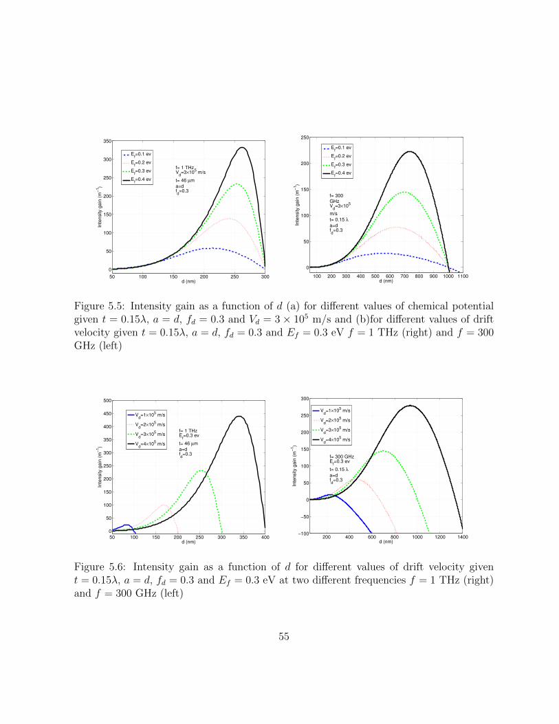
50 100 150 200 250 300
0
50
100
150
200
250
300
350
d (nm)
Inte
nsity g
ain
(m
−1)
Ef=0.1 ev
Ef=0.2 ev
Ef=0.3 ev
Ef=0.4 ev
f= 1 THzV
d=3×10
5 m/s
t= 46 µm
a=dfd=0.3
100 200 300 400 500 600 700 800 900 1000 1100
0
50
100
150
200
250
d (nm)
Inte
nsity g
ain
(m
−1)
Ef=0.1 ev
Ef=0.2 ev
Ef=0.3 ev
Ef=0.4 ev
f= 300GHzV
d=3×10
5
m/s
t= 0.15 λ
a=dfd=0.3
Figure 5.5: Intensity gain as a function of d (a) for different values of chemical potentialgiven t = 0.15λ, a = d, fd = 0.3 and Vd = 3× 10⁵ m/s and (b)for different values of driftvelocity given t = 0.15λ, a = d, fd = 0.3 and Ef = 0.3 eV f = 1 THz (right) and f = 300GHz (left)
50 100 150 200 250 300 350 400
0
50
100
150
200
250
300
350
400
450
500
d (nm)
Inte
nsity g
ain
(m
−1)
Vd=1×10
5 m/s
Vd=2×10
5 m/s
Vd=3×10
5 m/s
Vd=4×10
5 m/s
f= 1 THzE
f=0.3 ev
t= 46 µm
a=dfd=0.3
200 400 600 800 1000 1200 1400−100
−50
0
50
100
150
200
250
300
d (nm)
Inte
nsity g
ain
(m
−1)
Vd=1×10
5 m/s
Vd=2×10
5 m/s
Vd=3×10
5 m/s
Vd=4×10
5 m/s
f= 300 GHzE
f=0.3 ev
t= 0.15 λ
a=dfd=0.3
Figure 5.6: Intensity gain as a function of d for different values of drift velocity givent = 0.15λ, a = d, fd = 0.3 and Ef = 0.3 eV at two different frequencies f = 1 THz (right)and f = 300 GHz (left)
55
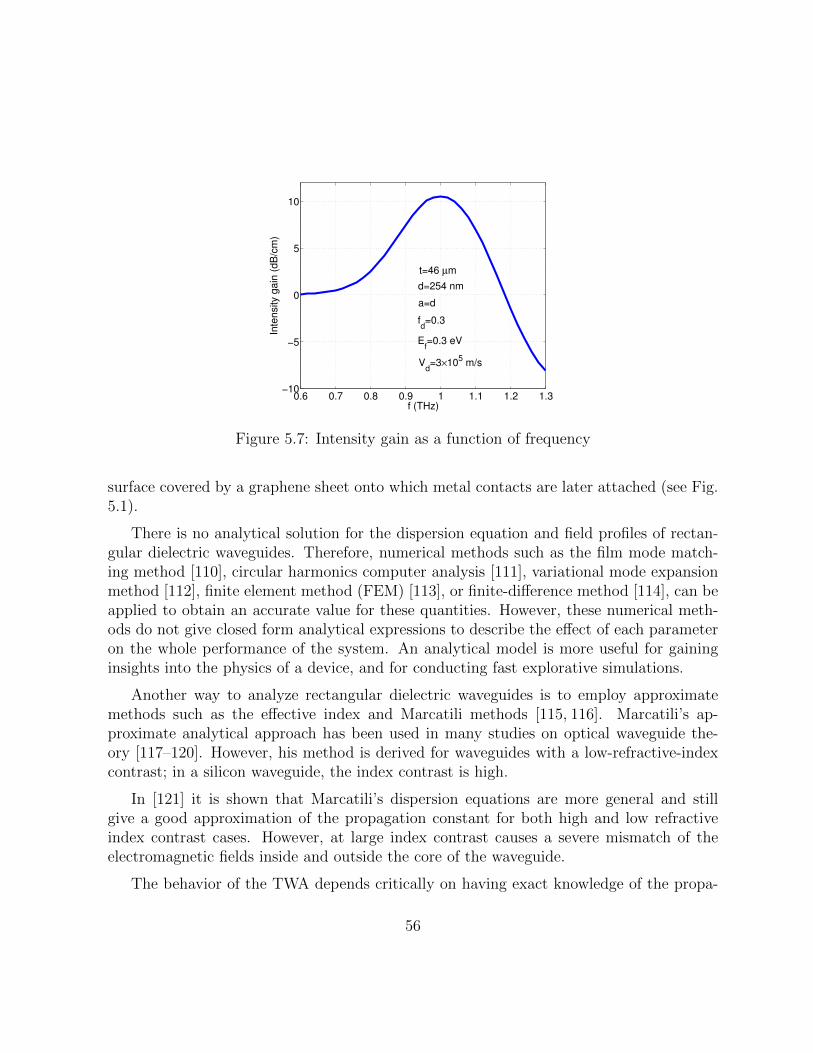
0.6 0.7 0.8 0.9 1 1.1 1.2 1.3−10
−5
0
5
10
f (THz)
Inte
nsity g
ain
(d
B/c
m)
Vd=3×10
5 m/s
Ef=0.3 eV
t=46 µm
d=254 nm
fd=0.3
a=d
Figure 5.7: Intensity gain as a function of frequency
surface covered by a graphene sheet onto which metal contacts are later attached (see Fig.5.1).
There is no analytical solution for the dispersion equation and field profiles of rectan-gular dielectric waveguides. Therefore, numerical methods such as the film mode match-ing method [110], circular harmonics computer analysis [111], variational mode expansionmethod [112], finite element method (FEM) [113], or finite-difference method [114], can beapplied to obtain an accurate value for these quantities. However, these numerical meth-ods do not give closed form analytical expressions to describe the effect of each parameteron the whole performance of the system. An analytical model is more useful for gaininginsights into the physics of a device, and for conducting fast explorative simulations.
Another way to analyze rectangular dielectric waveguides is to employ approximatemethods such as the effective index and Marcatili methods [115, 116]. Marcatili’s ap-proximate analytical approach has been used in many studies on optical waveguide the-ory [117–120]. However, his method is derived for waveguides with a low-refractive-indexcontrast; in a silicon waveguide, the index contrast is high.
In [121] it is shown that Marcatili’s dispersion equations are more general and stillgive a good approximation of the propagation constant for both high and low refractiveindex contrast cases. However, at large index contrast causes a severe mismatch of theelectromagnetic fields inside and outside the core of the waveguide.
The behavior of the TWA depends critically on having exact knowledge of the propa-
56

gating modes on the top surface of the waveguide where the interaction with electrons ingraphene happens. To get a good approximation of the interaction impedance, an improvedform of the modal field based on Marcatili’s approach is used. This modal electromagneticfield has a lower mismatch for the same dispersion equations.
Figure 5.8: Depiction of fulfilled and unfulfilled boundary conditions for Marcatili, andimproved Marcatili methods. At each interface, fields that satisfy boundary conditions areshown in green, all others are in red. Regions 1-5 are defined in top left picture.
Detailed descriptions of the Marcatili method and the improved method are given inappendices C and D, respectively. The field distributions obtained from both methods
57

500 1000 1500 2000 2500 3000 3500 4000a ( m)
10-6
10-4
10-2
100
102
Uer
(J/
m3)
Marctili Hx=0
Improved Hx=0
Marctili Ey=0
Improved Ey=0
Figure 5.9: Normalized mismatch energy density of Ex11 mode at core interfaces, Uer (eq.5.38), for b = 600µm at f = 150GHz. Comparison of four methods calculating fielddistribution of Ex11 mode.
are not exact solutions of Maxwell’s equations. The solutions obey Maxwell’s equationsin all regions individually. However, all boundary conditions at the interfaces betweenthe waveguide core and its cladding cannot be satisfied at the same time. The differencebetween these methods is in choosing which boundary conditions to satisfy.
Marcatilis methods (original and improved) are summarized in Fig. 5.8. At eachinterface, the fields that satisfy the boundary conditions are shown in green, all others areshown in red.
The modes in a rectangular waveguide are divided into two families: Exnm modes,where most of the electric field is polarized in the x-direction; and Eynm modes, where mostof the electric field is in the y-direction. The subscripts n and m represent, respectively,the number of field extrema along the x and y directions. Our analysis considers onlythe Ex11 mode, a TM-like mode at the top surface of the waveguide where the grapheneis located. The coupling between the space charge density wave in the graphene and theTE-like mode (Eynm) is not significant, since the z-directed plasma wave is modulated onlyby the z component of the electric field.
Both the improved Hx=0 method and improved Ey=0 method give better estimationof the fields than their corresponding Marcatili method. To demonstrate this, the discon-
58
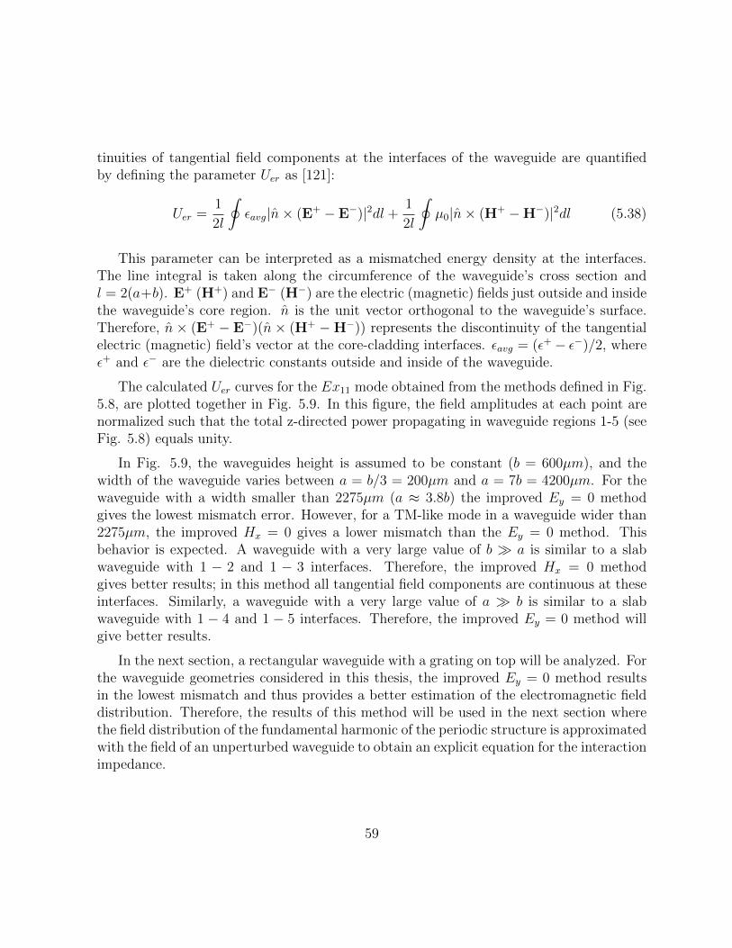
tinuities of tangential field components at the interfaces of the waveguide are quantifiedby defining the parameter Uer as [121]:
Uer =1
2l
∮εavg|n× (E+ − E−)|2dl +
1
2l
∮µ0|n× (H+ −H−)|2dl (5.38)
This parameter can be interpreted as a mismatched energy density at the interfaces.The line integral is taken along the circumference of the waveguide’s cross section andl = 2(a+b). E+ (H+) and E− (H−) are the electric (magnetic) fields just outside and insidethe waveguide’s core region. n is the unit vector orthogonal to the waveguide’s surface.Therefore, n × (E+ − E−)(n × (H+ −H−)) represents the discontinuity of the tangentialelectric (magnetic) field’s vector at the core-cladding interfaces. εavg = (ε+ − ε−)/2, whereε+ and ε− are the dielectric constants outside and inside of the waveguide.
The calculated Uer curves for the Ex11 mode obtained from the methods defined in Fig.5.8, are plotted together in Fig. 5.9. In this figure, the field amplitudes at each point arenormalized such that the total z-directed power propagating in waveguide regions 1-5 (seeFig. 5.8) equals unity.
In Fig. 5.9, the waveguides height is assumed to be constant (b = 600µm), and thewidth of the waveguide varies between a = b/3 = 200µm and a = 7b = 4200µm. For thewaveguide with a width smaller than 2275µm (a ≈ 3.8b) the improved Ey = 0 methodgives the lowest mismatch error. However, for a TM-like mode in a waveguide wider than2275µm, the improved Hx = 0 gives a lower mismatch than the Ey = 0 method. Thisbehavior is expected. A waveguide with a very large value of b � a is similar to a slabwaveguide with 1 − 2 and 1 − 3 interfaces. Therefore, the improved Hx = 0 methodgives better results; in this method all tangential field components are continuous at theseinterfaces. Similarly, a waveguide with a very large value of a � b is similar to a slabwaveguide with 1 − 4 and 1 − 5 interfaces. Therefore, the improved Ey = 0 method willgive better results.
In the next section, a rectangular waveguide with a grating on top will be analyzed. Forthe waveguide geometries considered in this thesis, the improved Ey = 0 method resultsin the lowest mismatch and thus provides a better estimation of the electromagnetic fielddistribution. Therefore, the results of this method will be used in the next section wherethe field distribution of the fundamental harmonic of the periodic structure is approximatedwith the field of an unperturbed waveguide to obtain an explicit equation for the interactionimpedance.
59

Figure 5.10: High-resistivity silicon waveguide with surface corrugation.
5.3.1 Analysis of Floquet modes in a rectangular dielectric waveg-uide with a grating on top
This thesis presents an approximate analytical solution for electromagnetic wave propaga-tion in a dielectric rectangular waveguide grating. In the previous section, a similar anal-ysis was done for TE and TM mode propagation in a thin film dielectric waveguide witha grating on the top surface. The current section covers a more-rigorous analysis of hy-brid modes in a rectangular dielectric waveguide that is more applicable for monolithicintegrated circuits.
The analytic expressions for the space harmonics of the electromagnetic field, and theinteraction impedance, are obtained by means of an approximate Floquet mode analysis.In a TWA, the interaction impedance is a measure of the coupling between the electricfield and the electron beam in the interaction region for a given electromagnetic power.It is an important parameter in determining the gain and efficiency of the amplifier. Theapproximate theoretical procedure is well-suited to generating design data for dielectricgrating structures. For instance, using this technique in this thesis, the influences ofphys- ical dimensions on the interaction impedance are explored. The dimensions of therectangular waveguide and the grating are determined to obtain the optimum interactionimpedance.
The structure under investigation is depicted in Fig. 5.11 The structure is composed ofa rectangular high-resistivity silicon waveguide with surface corrugation. Recently, it wasdemonstrated in [98,99] that such a waveguide is very low loss at sub-millimeter-wave andTHz frequencies. A high precision fabrication process for this structure is also presented.
The electromagnetic waves propagating along a straight waveguide are classified intoTE, TM or hybrid modes according to the presence or absence of the longitudinal field com-ponents Ez and Hz. The dielectric rectangular waveguide can only support hybrid modes
60

Figure 5.11: Cross section of waveguide with grating layer on top (denoted by “P”).
with both Ez and Hz present. Consider a monochromatic wave with angular frequency ω,propagating in the z direction with a propagation constant βz. In a homogeneous regionj, with a relative dielectric constant of εr = εrj = cons, all components satisfy the reducedwave equation (here given only for Ez)
∇2tEz +K2
jEz = 0 (5.39)
where K2j = k2
0εrj − β2z , and ∇t is the transverse Laplacian.
The grating structure is modelled by a thin inhomogeneous layer of thickness tg, char-acterized by the dielectric constant εg(z), which varies periodically along the propagationdirection z. The wave equations for Ez and Hz in this layer are
∇2Ez +∂
∂z
[∂ln(εg(z))
∂zEz
]+ ω2µ0εg(z)Ez = 0 (5.40a)
∇2Hz + ω2µ0εg(z)Hz = 0 (5.40b)
Using Maxwell’s equations, all electromagnetic field components can be obtained from thelongitudinal field components. In the grating region with the εg(z) = ε0εrg(z) function of
61

500 550 600 650 700 750 800 850 900 950 1000
b ( m)
104
105
106
K12
a=115 m
a=120 m
a=135 m
a=150 m
Figure 5.12: Coupling factor as a function of b for different values of a with lp = 300nm,tg = 300nm and md = 0.3 at f = 150GHz.
z, we have
k20εrg(z)Ex +
∂2Ex∂z2
=∂2Ez∂z∂x
− jωµ∂Hz
∂y(5.41a)
k20εrg(z)Ey +
∂2Ey∂z2
=∂2Ez∂z∂y
+ jωµ∂Hz
∂y(5.41b)
k20εrg(z)Hx −
∂ ln εg(z)
∂z
∂Hx
∂z+∂2Hx
∂z2= jωεg
∂Ez∂y
+∂2Hz
∂z∂x− ∂ ln εg(z)
∂z
∂Hz
∂x(5.41c)
k20εrg(z)Hy −
∂ ln εg(z)
∂z
∂Hy
∂z+∂2Hy
∂z2= jωεg
∂Ez∂y
+∂2Hz
∂z∂x− ∂ ln εg(z)
∂z
∂Hz
∂x(5.41d)
In a homogeneous region, the above equations (5.40,5.41) are simplified by substituting∂ ln εg(z)/∂z equal to zero.
In a rectangular dielectric waveguide with a periodic dielectric layer, the field compo-
62

50 100 150 200 250 300
a ( m)
103
104
105
106
K12
b=500 m
b=600 m
b=700 m
Figure 5.13: Coupling factor as a function of a for different values of b with lp = 300nm,tg = 300nm and md = 0.3 at f = 150GHz.
nents are in the Floquet form:
Hz =∞∑−∞
hzm(x, y)e−jβzmz (5.42a)
Ez =∞∑−∞
ezm(x, y)e−jβzmz (5.42b)
where βzm = βz0 + 2mπd
. Similar equations are applied for the x and y field components.
The relative dielectric constant of the grating layer with periodic dielectric constant,εg = ε0εrg, can be expressed by its Fourier series expansion
εrg = εrg0 +∞∑1
εrgm cos(2πm
dz) (5.43)
Substituting the Floquet expansion of the field components (5.42), along with the first-
order Fourier expansion of εrg = εrg0 + εrg1 cos(2πdz) and ∂ ln(εrg)
∂z= g1 sin(2π
dz) into equation
63

50 100 150 200 250 300 350 400 450 500 550 600
a ( m)
0.5
1
1.5
2
2.5
3
z/k
0
b=600 m
First mode
Second mode
500 550 600 650 700 750 800 850 900 950 1000
b ( m)
0.4
0.6
0.8
1
1.2
1.4
1.6
z/k
0
a=120 m
First mode
Second mode
Figure 5.14: (a) Normalized dispersion diagram of uniform rectangular silicon waveguideversus a with b = 600µm. (b) Normalized dispersion diagram versus b with a = 120µm.
(5.40) and (5.41) yields∑m
(∇2t − β2
zm + k20εrg0
)hzm(x, y)e−jβzmz+
k20εrg1/2
[∑m
hzme−jβz(m−1)z +
∑m
hzme−jβz(m+1)z
]= 0
(5.44)
∑m
(∇2t − β2
zm + k20εrg0
)ezme
−jβzmz+∑m
(k2
0εrg1/2 + g1π/d− βzmg1/2)ezme
−jβz(m−1)z+∑m
(k2
0εrg1/2 + g1π/d+ βzmg1/2)ezme
−jβz(m+1)z = 0
(5.45)
∑m
(k2
0εrg0 − β2zm
)eyme
−jβzmz +∑m
k20εrg12
eyme−jβz(m−1)z +
∑m
k20εrg12
ey(m)e−jβz(m+1)z
= −∑m
jβzm∂ezm∂y
e−jβzmz +∑m
jωµ0∂hzm∂x
e−jβzmz
(5.46)
64

∑m
(k2
0εrg0 − β2zm
)hyme
−jβzmz+
∑m
(k2
0εrg12
+g1βzm
2
)hyme
−jβz(m−1)z +∑m
(k2
0εrg12− g1βzm
2
)hyme
−jβz(m+1)z
= −∑m
jβzm∂hzm∂y
e−jβzmz − g1
2j
[∑m
∂hzm∂y
e−jβz(m−1)z −∑m
∂hzm∂y
e−jβz(m+1)z
]
−∑m
jωε0εrg0∂ezm∂x
e−jβzmz − jωε0εrg12
[∑m
∂ezm∂x
e−jβz(m−1)z +∑m
∂ezm∂x
e−jβz(m+1)z
](5.47)
Due to the uniqueness of the Fourier series expansion, we have:
∇2thzm −G2
pmhzm = −k20
εrg12
(hz(m−1) + hz(m+1)
)(5.48)
∇2t ezm −G2
pmezm =−[k2
0εrg12
+g1βz(m−1)
2+g1π
d
]ez(m−1)
−[k2
0εrg12−g1βz(m−1)
2+g1π
d
]ez(m+1)
(5.49)
eym =k2
0εrg12G2
pm
(ey(m−1) + ey(m+1)
)+jβzmG2pm
∂ezm∂y− jωµ0
G2pm
∂hzm∂x
(5.50)
hym =k2
0εrg12G2
pm
(hy(m−1) + hy(m+1)
)g1
2G2pm
(βz(m+1)hy(m+1) − βz(m−1)hy(m−1)
)− jβzmG2pm
∂hzm∂y− jg1
2G2pm
(∂hz(m−1)
∂y−∂hz(m+1)
∂y
)− jωε0εrg0
G2pm
∂ezm∂x− jωε0εrg1
2G2pm
(∂ez(m−1)
∂x+∂ez(m+1)
∂x
)(5.51)
65

where G2pm = β2
zm − ω2µ0ε0εrg0. This set of equations couples each space harmonic to thenext lower and higher harmonics. If higher order Fourier terms of εrg (5.43) are considered,more harmonic terms will appear. The higher-order space harmonics have amplitudesmuch smaller than those of the lower-order space harmonics. Therefore, the first-orderapproximation is applied to simplify the above equations. In this approximation, to obtainthe solution for the first-order space harmonic (m=1), the second-order space harmonic(m=2) is neglected with respect to the zeroth-order space harmonic.
∇2thz1 −G2
p1hz1 = −k20
εrg12hz0 (5.52)
∇2t ez1 −G2
p1ez1 = −[k2
0εrg12
+g1βz0
2+g1π
d
]ez0 (5.53)
ey1 =jβz1G2p1
∂ez1∂y− jωµ0
G2p1
∂hz1∂x
+k2
0εrg12G2
p1
ey0 (5.54)
hy1 = −jβz1G2p1
∂hz1∂y− jωε0εrg0
G2p1
∂ez1∂x
− jg1
2G2p1
∂hz0∂y− jωε0εrg1
2G2p1
∂ez0∂x
+k2
0εrg1 − g1βz02G2
p1
hy0
(5.55)
For a waveguide with a thin grating, the zeroth-order space harmonic can be approxi-mated by the modal solution of the rectangular waveguide with no grating. As was men-tioned in the introduction, there is no analytic solution for the field distribution of a rect-angular dielectric waveguide. Therefore, the field distributions obtained from the improvedMarcatili Ey = 0 method (described in appendix D), are used as a good approximation forthe field distribution of the zeroth-order space harmonic.
ez0 = A2e−γx(x−b/2) cos(kyy) (5.56a)
hz0 = B2e−γx(x−b/2) sin(kyy) (5.56b)
ey0 =
(A2jβz0kyk2t2
−B2jωµγxk2t2
)e−γx(x−b/2) sin(kyy) (5.56c)
hy0 =
(A2jωε0εr2γx
k2t2
−B2jβkyk2t2
)e−γx(x−b/2) cos(kyy) (5.56d)
66

0 0.1 0.2 0.3 0.4 0.5 0.6 0.7 0.8 0.9 1
md
0
2
4
6
8
10
12
14
K12
105
tg=50 nm
tg=80 nm
tg=300 nm
(a)
0 50 100 150 200 250 300
tg (nm)
0
2
4
6
8
10
12
14
K12
105
md=0.1
md=0.3
md=0.5
(b)
Figure 5.15: (a) Coupling factor versus md for different values of tg; and (b) interactionimpedance versus tg for different values of md with a = 115µm, b = 600µm at f = 150GHz
where A2 and B2 coefficients are defined by eq.D.1.
5.3.2 Derivation of the field distribution of the first-order spaceharmonic
Because the first order space harmonic field is confined mainly to the grating layer, its fielddistribution can be defined only for the grating layer and surrounding areas, assuming thefield distribution to be negligible in other areas. Figure 5.11 shows a cross section of therectangular waveguide with a thin grating layer on top denoted by the letter ”P”. The field
67

of the first-order harmonic inside regions 1, 2, and P, is a standing wave in y direction, andit decays in proportion to its distance from the interfaces of the P layer in the x direction.For a thick rectangular waveguide, it can be assumed that the field decays completely insilicon layer 1; thus, no field of the first order harmonic reaches layer 3 under the siliconlayer.
Since most of the first order space harmonic’s power is concentrated in layer P (asin Marcatili’s approach), the field at the corner areas 1L,R and 2L,R can be neglected.Furthermore, in regions PR and pL, the field decays in y direction from the interfaces ofthe grating layer. Thus, for a thin layer of grating when its thickness, tg, is much smallerthan its width, a, the field in regions pL and pR can also be neglected. The analysis of a2D slab structure presented in the previous section, showed that although the interactionimpedance is higher for thicker grating layers, it does not change for gratings thicker thantg = d, where d is the pitch of the grating (Fig. 5.3). Therefore, the assumption tg << acan be applied for the structure in question in which t is in the order of a few hundrednanometers and a is in the order of tens of micrometers.
By considering all of the above-mentioned assumptions, the Hz1 = hz1e−jβz1z and Ez1 =
ez1e−jβz1z field components of the first-order space harmonic can be represented as:
ez1 =
a2e−γx2(x−b/2−tg) cos(kyy) x > b/2 + tg[
ap sinh(γxp(x− b/2)) + a′p cosh(γxp(x− b/2))f ′
G2p1
][−A2
f ′e−γx(x−b/2)
γ2x − k2
y −G2p1
]cos(kyy) b/2 < x < b/2 + tg
a1eγx1(x−b/2) cos(kyy) x < b/2
(5.57)
hz1 =
b2e−γx2(x−b/2−tg) sin(kyy) x > b/2 + tg[
bp cosh(γxp(x− b/2)) + b′p sinh(γxp(x− b/2))−B2fe−γx(x−b/2)
γ2x − k2
y −G2p1
]sin(kyy) b/2 < x < b/2 + tg
b1eγx1(x−b/2) sin(kyy) x < b/2
(5.58)
68

where f =k20εr2
2and f ′ =
k20εr22
+ g1βz02
+ g1πd
. From the wave equations in 3 regions we have:
γ2x1 = β2
z1 + k2y − k2
0εair (5.59a)
γ2x2 = β2
z1 + k2y − k2
0εSi (5.59b)
γ2xp = β2
z1 + k2y − k2
0εrg0. (5.59c)
Since both the zeroth- and first-order harmonics are hybrids, both Ez and Hz com-ponents should be defined to obtain all other field components (Eq. 5.41). The ez1 andhz1 fields defined by equations 5.57 and 5.58, satisfy wave equations C.2 in homogeneouslayers 1 and 2, and satisfy the equations 5.53 and 5.52 for the periodic layer ”p”. Theseare inhomogeneous electromagnetic wave equations with ez0 and hz0 given in eq. 5.56.
Similarly, the ey1 and hy1 components are obtained from equations 5.54 and 5.3.1
ey1 =
[−a2
jβz1kyG2t2
+ b2jωµ0γx2
G2t2
]e−γx2(x−b/2−tg) sin(kyy) x > b/2 + tg
egy1 b/2 < x < b/2 + tg[−a1
jβz1kyG2t1
− b1jωµ0γx1
G2t1
]eγx1(x−b/2) sin(kyy) x < b/2
(5.60)
egy1 = −jβz1kyG2p1
[ap sinh(γxp(x− b/2)) + a′p cosh(γxp(x− b/2))− f ′A2
γ2x − k2
y −G2p1
e−γx(x−b/2)
]sin(kyy)
−jωµoG2p1
[γxp(bp cosh(γxp(x− b/2)) + b′p sinh(γxp(x− b/2))
)+
fB2
γ2x − k2
y −G2p1
γxe−γx(x−b/2)
]sin(kyy)
+k2
0εrg12G2
p1
(A2jβz0kyk2t2
−B2jωµ0γxk2t2
)e−γx(x−b/2) sin(kyy)
(5.61)
69

hy1 =
(−a2
jωε0εr2γx2
G2t2
+ b2jβz1kyG2t2
)e−γx2(x−b/2−tg) cos(kyy) x > b/2 + tg
hgy1 b/2 < x < b/2 + tg(a1jωε0εr1γx1
G2t1
+ b1jβz1kyG2t1
)eγx1(x−b/2) cos(kyy) x < b/2
(5.62)
hgy1 =jωε0εrg0G2p1
[γxp[ap cosh(γxp(x− b/2)) + a′p sinh(γxp(x− b/2))] + γx
f ′A2
γ2x − k2
y −G2p1
e−γx(x−b/2)
]cos(kyy)
+jβz1kyG2p1
[bp cosh(γxp(x− b/2)) + b′p sinh(γxp(x− b/2))− fB2
γ2x − k2
y −G2p1
e−γx(x−b/2)
]cos(kyy)
+k2
0εrg1 − g1βz02G2
p1
(A2jωε0εr2γx
k2t2
−B2jβz0kyk2t2
)e−γx(x−b/2) cos(kyy)
+
(−A2
jωε0εrg1γx2G2
p1
+B2jg1ky2G2
p1
)e−γx(x−b/2) cos(kyy)
(5.63)
where G2t1 = B2
z1− k20εSi and G2
t2 = B2z1− k2
0εair. The eight unknown coefficients (a1,2,p,b1,2,p, a
′p, and b′p coefficients in equations5.57 and 5.58) are obtained from the boundary
conditions. Since the field is considered non-negligible only in regions 1, 2, and p, theboundary conditions are the continuity of Ez, Hz, Ey and Hy components at the top andbottom grating layer interfaces, resulting in 8 equations. By solving these 8 equations with8 unknowns, the field distribution coefficients are obtained.
The next step is to use the field distribution of the first-order space harmonic modedefined in this section to obtain the interaction impedance of the proposed TWA describedin the beginning of this chapter (Fig. 5.1)
5.3.3 Gain and dispersion equations
Similar to the discussion focused on slab waveguides (section 5.2.2), the field of the spaceharmonic excited by the surface current of J = Jee
−jβz can be obtained for the top-gratedrectangular waveguide from eq. 5.5, substituting EA1 = As cos(kyy)z and Je = Js cos(kyy)z
70

E1(xg, y) =−j|As|2 (a+ sin(kya)/ky)
8PA0(β1 − β)Js cos(kyy) (5.64)
where As = ap sinh(γxptg) + a′p cosh(γxptg) − A2f ′e−γxtg
γ2x−k2y−G2p1
(eq. 5.53). PA0 is calculated by
integrating the z component of the Poynting vector P = 12E×H∗ over the areas of all 1−5
regions using the field expressions given by equations C.3 and C.4.
The current induced by this electric field at the surface of the graphene is obtained fromOhm’s law (eq. 5.34). The dispersion equation is obtained by imposing a self-consistencycondition between equations 5.64 and 5.34:
−j|As|2 (a+ sin(kya)/ky)
8PA0(βz1 − βz)σ(βz, ω) = 1 (5.65)
This equation is similar to equation 5.35 given for the slab waveguide, except that in theformer, the term |EA1(x = xg, y = 0)|2 (1/2 + cos(kya)) replaces the term |EA1(x = xg)|in order to consider the variation of the electric field along the y axis. Also, the PA0 inthis equation is the total power carried by the first harmonic of the electric field. Similarto eq. 5.37 the gain equals g = 2Imβ = K1β
21Real(σ). For the rectangular structure, the
interaction impedance K1 is defined as:
K1 =|As|2 (a+ sin(kya)/ky)
4PA0β2z1
(5.66)
The amount of K1β21 determines the strength of the coupling between the electromag-
netic wave propagating in the rectangular waveguide and the space charge wave confinedto the graphene layer. The value of K1β
21 depends on both the waveguide dimensions, a
and b, and the grating dimensions, lp, tg and fd. These parameters should be optimizedto maximize the coupling factor.
Figure 5.12 and 5.13 show the value of K1β21 as a function of b and a for different
a and b values respectively, at the frequency of 150GHz with lp = 300nm, tg = 300nmand md = 0.3. These figures show that the maximum coupling is obtained when thepropagation constant of the waveguide is close to the cutoff point. Figure 5.14(a) and (b)show the dispersion plot of the uniform (without grating) rectangular waveguide versusa (with b = 600µm) and b (with a = 120µm), respectively. These plots are obtained bysolving equations C.7d and C.8d, given β2
0 = k20 − k2
x − k2y. Near the cutoff point, the field
of the rectangular waveguide is less confined to the core and therefore has more overlapwith the plasma wave at the graphene’s surface. The result is a larger coupling factor.
71

Figure 5.16: Normalized amplitude of second Fourier series coefficient∣∣∣a1a0 ∣∣∣ for rectangular
wavefrom, depicted in the inset, with A1 = 1 and A2 = 1/εSi.
Figure 5.15(a) and (b) shows the variation of K1β21 with respect to the filling factor
and depth of the grating, respectively, with lp = 300nm, a = 115µm and b = 600µmat f = 150GHz. The first-order space harmonic field at the surface of the grating isroughly similar to a periodic rectangular waveform. The Fourier series representation ofa rectangular waveform with the maximum of A1, minimum of A2, period of T , and dutycycle of D = τ
T(see inset of Fig. 5.16) is:
SΠ(t) =+∞∑
n=− inf
ane−j 2πn
Tt (5.67)
a0 = A2 +D(A1 − A2), an =(A1 − A2)
j2πn
(ej2πDn − 1
)(5.68)
The ratio of∣∣∣a1a0 ∣∣∣ versus D for A1 = 1 and A2 = 1/εSi is plotted in Fig. 5.16. This plot
is very similar to the plot depicted in Fig. 5.15(a).
The plots of Fig. 5.12, 5.12 and 5.15 are used to design the rectangular waveguideand the grating for the slow-wave structure of the TWA. The goal is to gain maximuminteraction impedance. The rectangular image waveguide is used instead of a rectangularrod waveguide. The image waveguide has the same thickness as the wafer being used.From among standard wafer thicknesses, 300µm was chosen; a thickness suitable for thefrequency band of ∼ 100GHz to 300GHz. The image waveguide structure is supported by
72
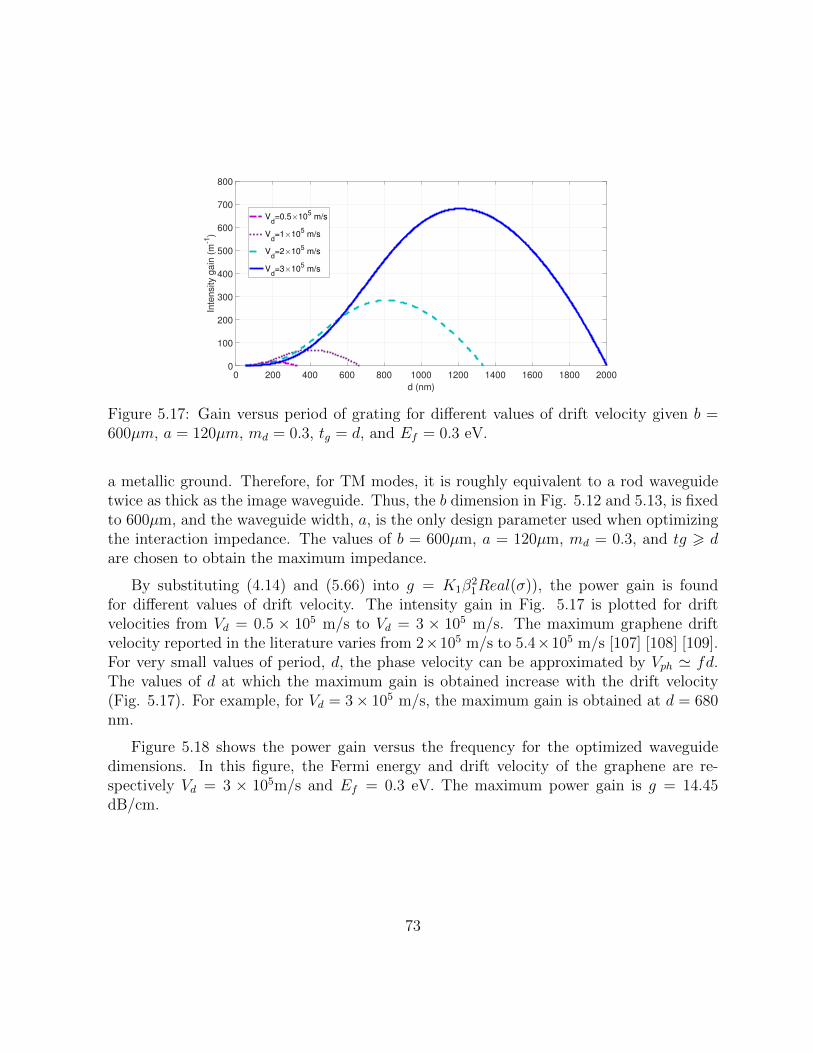
0 200 400 600 800 1000 1200 1400 1600 1800 2000
d (nm)
0
100
200
300
400
500
600
700
800
Inte
nsity g
ain
(m
-1)
Vd=0.5 10
5 m/s
Vd=1 10
5 m/s
Vd=2 10
5 m/s
Vd=3 10
5 m/s
Figure 5.17: Gain versus period of grating for different values of drift velocity given b =600µm, a = 120µm, md = 0.3, tg = d, and Ef = 0.3 eV.
a metallic ground. Therefore, for TM modes, it is roughly equivalent to a rod waveguidetwice as thick as the image waveguide. Thus, the b dimension in Fig. 5.12 and 5.13, is fixedto 600µm, and the waveguide width, a, is the only design parameter used when optimizingthe interaction impedance. The values of b = 600µm, a = 120µm, md = 0.3, and tg > dare chosen to obtain the maximum impedance.
By substituting (4.14) and (5.66) into g = K1β21Real(σ)), the power gain is found
for different values of drift velocity. The intensity gain in Fig. 5.17 is plotted for driftvelocities from Vd = 0.5 × 10⁵ m/s to Vd = 3 × 10⁵ m/s. The maximum graphene driftvelocity reported in the literature varies from 2×10⁵ m/s to 5.4×10⁵ m/s [107] [108] [109].For very small values of period, d, the phase velocity can be approximated by Vph ' fd.The values of d at which the maximum gain is obtained increase with the drift velocity(Fig. 5.17). For example, for Vd = 3× 10⁵ m/s, the maximum gain is obtained at d = 680nm.
Figure 5.18 shows the power gain versus the frequency for the optimized waveguidedimensions. In this figure, the Fermi energy and drift velocity of the graphene are re-spectively Vd = 3 × 10⁵m/s and Ef = 0.3 eV. The maximum power gain is g = 14.45dB/cm.
73
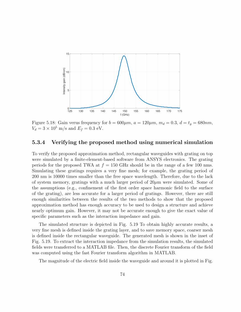
125 130 135 140 145 150 155 160 165 170 175
f (GHz)
0
5
10
15
Inte
nsity g
ain
(dB
/cm
)
Figure 5.18: Gain verus frequency for b = 600µm, a = 120µm, md = 0.3, d = tg = 680nm,Vd = 3× 10⁵ m/s and Ef = 0.3 eV.
5.3.4 Verifying the proposed method using numerical simulation
To verify the proposed approximation method, rectangular waveguides with grating on topwere simulated by a finite-element-based software from ANSYS electronics. The gratingperiods for the proposed TWA at f = 150 GHz should be in the range of a few 100 nms.Simulating these gratings requires a very fine mesh; for example, the grating period of200 nm is 10000 times smaller than the free space wavelength. Therefore, due to the lackof system memory, gratings with a much larger period of 20µm were simulated. Some ofthe assumptions (e.g., confinement of the first order space harmonic field to the surfaceof the grating), are less accurate for a larger period of gratings. However, there are stillenough similarities between the results of the two methods to show that the proposedapproximation method has enough accuracy to be used to design a structure and achievenearly optimum gain. However, it may not be accurate enough to give the exact value ofspecific parameters such as the interaction impedance and gain.
The simulated structure is depicted in Fig. 5.19 To obtain highly accurate results, avery fine mesh is defined inside the grating layer, and to save memory space, coarser meshis defined inside the rectangular waveguide. The generated mesh is shown in the inset ofFig. 5.19. To extract the interaction impedance from the simulation results, the simulatedfields were transferred to a MATLAB file. Then, the discrete Fourier transform of the fieldwas computed using the fast Fourier transform algorithm in MATLAB.
The magnitude of the electric field inside the waveguide and around it is plotted in Fig.
74

Figure 5.19: Simulated silicon image waveguide. Inset shows generated mesh.
5.20. Figure 5.21 shows the Ez component of the electric field in the middle of the surfaceof the grating along the z-direction (line lz in Fig. 5.19). It consists of rapid fluctuationswith a slowly varying sinusoidal envelope. The slow varying sinusoidal envelope is thefundamental harmonic, while the rapid fluctuations are caused by first and higher orderharmonics. To obtain the exact amplitude of each harmonic, the Fourier transform of thefield distribution along the z direction is calculated (see Fig. 5.22). The ky parameter in(5.66) is obtained by fitting a cosine, cos(kyy) function to the field distribution of the fieldalong the y direction inside the rectangular waveguide (see Fig. 5.23). The propagatedpower P is the same as the source power defined by the input port.
In Fig. 5.24, the coupling factor versus b obtained from the approximate analysis isplotted together with that obtained from the simulations. The guided modes in an infinitedielectric slab waveguide have propagation constants greater than k0. The propagationconstant depends on the slab thickness. The thickness at which the propagation constantbecomes βz = k0 is called the cutoff thickness. Waveguides with thicknesses larger than thiscutoff thickness have at least one guided mode. For smaller profiles, all modes are radiatingmodes andwhich are not confined by the dielectric core. For a rectangular waveguide witha finite width, the cutoff thickness is smaller than the cutoff thickness of anthe infinite slab
75

Figure 5.20: Magnitude of electric field vector simulated by ANSYS electronics software.
waveguide. However, there is no exact analytical solution to find the cutoff thickness ina rectangular waveguide. In Fig. 5.24, theoretical results are plotted only for b values atwhich βz > k0; simulation results are plotted also for smaller values of b at which guidedmodes were observed in simulation.
In Fig. 5.24, both the approximate analytical and numerical results show that the inter-action impedances decrease, away from the cutoff point, when the width of the waveguideis increased. However, near the cutoff point, the interaction impedance calculated usingthe proposed approximate analytical method increases exponentially; the numerical resultshows only a relatively small peak near this point.
The difference near the cutoff point comes from the large discrepancy between the exactfield distribution of the electromagnetic field and the estimated field distribution obtainedfrom the improved Marcatili method. This method is based on the assumption that thefield is confined inside the waveguides core which is not valid near the cutoff point. As itis shown in Fig. 5.24, away from the cutoff point, there is good agreement between theapproximate analytical and simulation results. Also, where an analytical solution existsfor the slab waveguide, there is good agreement between the approximate analytical and
76

-2 -1.5 -1 -0.5 0 0.5 1 1.5 2
z (mm)
-1
-0.5
0
0.5
1
Ez (
V/m
)
105
Figure 5.21: Ez component of electric field on surface of grating along line lz (see Fig.5.19), for a = 125µm, b = 600µm, md = 0.3, tg = 10µm, and lp = 20µm at f = 150GHz.
simulation results (see Fig. 5.3).
Equation (5.66) can also be written as:
K1 =|As|2
|A2|2|A2|2 (1 + sin(kya)/ky)
4PA0β21
(5.69)
The expression on the left is a multiplication of two terms. The first term, |As|2
|A2|2 (A2 is
defined in eq. D.2), represents the amplitude of the first-order space harmonic generatedby the grating layer with respect to the fundamental harmonic. This term is determinedmainly by the grating dimensions. The second term shows how much of the power isdistributed along the surface of the grating. For thin gratings, it is mainly determined bythe waveguide dimensions.
Figure 5.25 shows the term |As||A2| versus md for a grating with tg = 10µm on top of a
rectangular waveguide with a = 125µm and b = 600µm. The normalized amplitude of thefirst-order space harmonic obtained from the approximate theoretical analysis is maximizedatmd = 0.3. However, for the values obtained from simulation, it is maximized atmd = 0.4.As mentioned above, the normalized amplitude of the first-order space harmonic of therectangular periodic field is maximized for a duty cycle of 0.3. For very small gratingperiods (small with respect to the wavelength of propagation), the field at the surface ofthe grating is very similar to the periodic rectangular wave. This approximation becomesless accurate for larger grating periods, justifying the difference between the approximate
77

-2 0 2
F (m-1
) 106
0
2
4
6F
FT
104
X: 3874
Y: 5.913e+04
X: 3.102e+05
Y: 3.29e+04
Figure 5.22: Fourier series transform of Ez component depicted in Fig. 5.21.
analytical and simulation results for a grating period of 20µm.
In chapters 3 and 4, (when calculating the conductivity of the graphene layer), and inthis chapter (when calculating the dispersion equation from eq. 5.65), it is assumed that theelectromagnetic field exciting the space charge density wave in the graphene has only thez-component on the surface of the graphene, parallel to the direction of the drifting current.The TM modes of an infinite slab waveguide have only the Ez component. However, hybridmodes in a dielectric rectangular waveguide have both Ey and Ez components at the surfaceof the graphene. In this case, for an exact analysis of the graphene, a conductivity tensorσ =
( σyy σyzσzy σzz
)should be defined. The z- and y-components of the electric field are coupled
through hydrodynamic equations, increasing the complexity of the analysis drastically.
Therefore, we have assumed that the Ey component of the first-order space harmonicis negligible with respect to its Ez component. To verify the accuracy of this assumption,the Ey field on the surface of the grating along the z direction for a = 125µm, b = 600µm,md = 0.7, tg = 10µm, and lp = 20µm at f = 150GHz is plotted in Fig. 5.26. Comparingthe two plots of Fig. 5.21 and 5.26, it can be seen that Ey of the first-order space harmonic
78

Figure 5.23: Field distribution of the field along y direction. Solid line is simulated field;dotted line is fitted curve; and colored area indicates inside of silicon waveguide.
is one order of magnitude smaller than its Ez component.
5.4 Conclusion
In this chapter, an analytic solution is presented to analyze electromagnetic wave propa-gation in a periodic structure in the presence of graphene. Analytic expressions are alsogiven for the interaction impedance and gain of a proposed TWA. Within these expres-sions, each parameters individual effect on the overall performance of the structure isstudied. Throughout the chapter, the approximations made for this method along withthe conditions under which these approximations are valid are discussed.
The main contribution of this chapter has been to introduce an approximate theoreticalmethod for analyzing Floquet modes in gratings on top of rectangular dielectric waveguides.This method gives explicit expressions for the interaction impedance of slow-wave gratingstructures, which are then used to design the waveguide and grating.
To verify the proposed approximation method, the results obtained with this methodare compared with simulation results. To adjust the mesh size in accordance with thesystem memory, the period of the simulated gratings was set to be much larger than whatis required for the proposed graphene TWA. Therefore, the simulation results are used onlyfor verification of the theoretical results.
79

500 550 600 650 700 750 800 850 900 950 1000b ( m)
0
0.5
1
1.5
2
2.5
K12
104
a=125 mApproximate analysisSimulation
Figure 5.24: Coupling factor versus b with a = 125µm, md = 0.3, tg = 10µm, andlp = 20µm at f = 150GHz. Results obtained using proposed approximate theoreticalmethod (solid line); results obtained from simulation (dots).
Some of the assumptions made in the approximate theoretical method, such as theconfinement of the first order space harmonic field to the surface of the grating, are lessaccurate for larger periods of gratings. However, there are still enough similarities betweenthe results of the two methods to show that the approximate method is accurate enough fordesigning structures with nearly optimum gain. However, it may not be accurate enoughto give the exact value of parameters such as the interaction impedance and gain.
The dimensions of the rectangular waveguide and the grating have now been deter-mined. The next step, described in Chapter 6, is to fabricate the designed sample andverify the theoretical results with measurement results.
80

0.1 0.2 0.3 0.4 0.5 0.6 0.7 0.8 0.9
md
0
0.1
0.2
0.3
0.4
0.5
0.6
Norm
aliz
ed a
mplit
ude o
f e
z1
Approximate analysis
Simulation
a=125 m
b=600 m
Figure 5.25: Normalized amplitude of first-order space harmonic as function of md. Resultsobtained using proposed approximate theoretical method (solid line); results obtained fromsimulation (dots).
-2 -1 0 1 2
z (mm)
-4000
-2000
0
2000
4000
Ey (
V/m
)
Figure 5.26: Ey component of electric field on surface of grating along line lz (see Fig.5.19), for a = 125µm, b = 600µm, md = 0.3, tg = 10µm, and lp = 20µm at f = 150GHz.
81

Chapter 6
Fabrication and measurement
The proposed structure, depicted in Fig. 5.1, was created in three main stages (see Fig.6.1):
• Fabrication of the grating. (6.1)
• Transfer of the graphene layer and fabrication of the DC bias contacts. (6.2)
• Fabrication of the silicon waveguide.(6.3)
This chapter details the steps taken in each stage of the fabrication process. Theproposed travelling amplifier could have been designed and fabricated for use at 1 THzfrequency (the frequency of interest in this thesis so far); however, to simplify and speedup the fabrication process, the prototype structure was fabricated for a frequency rangeof 110-170 GHz. The fabrication of such a device at 1 THz is more complicated, for twomain reasons. The first reason is the long grating with smaller pitch. Because this gratingis fabricated using the Electron Beam Lithography (EBL) method, a good electron beamfocus is crucial and even a small change in height will knock the electron beam out of focus.This focus issue becomes more problematic for certain large area samples that require ahomogeneous structure, and it is very difficult to overcome in small structures becausehigher resolution is required. The solution is to divide the large area into smaller parts,then align and pattern each separately, after refocusing the beam on the individual partsin series. Unfortunately, this is a time-consuming process.
For frequencies around 100 GHz to 400 GHz, a simple image silicon waveguide ( [122]),a stand-alone waveguide that can be moved without having to be mounted on a handler,
82

Figure 6.1: Three main stages of the fabrication process.
was used. However, at 1THz, this type of waveguide become very lossy; moreover, itsvery delicate structure means it should be mounted on a handling structure ( [98,99,123]).This is the second reason why fabricating the structure at higher frequencies is morecomplicated. For these reasons a frequency of around 150 GHz was selected for fabricatingthe first prototype structure for proof of concept.
Various methods of etching and thin film deposition are known. In each step of thefabrication process, a suitable method whose outcome meets the required specifications wasselected based on the advantages and disadvantages of each method. These are describedin detail below.
There are two major types of etching: wet and dry. Wet etching uses liquid chemicals, usually mixtures of acids, bases, and/or solvents. The surface material is removed bychemical reactions. This form of etching is generally isotropic, and the material is etcheduniformly in all directions. This can lead to undercutting, as the underlying film is etchedfrom underneath the mask (Fig 6.2). Therefore, straight vertical walls cannot be fabricatedand undercuts always exist. However, the chemical nature of the etch can lead to goodetch selectivity, which is the main advantage of this method. Selectivity is the ratio ofthe underlying film etch rate to the mask etch rate. However, it is essentially isotropic.If anisotropic etching is desired, directionality must be induced into the etch process, andthis can be achieved by dry etching.
83

Figure 6.2: Schematic of (a) isotropic wet etching with undercut and (b) anisotropic dryetching with straight vertical walls.
Dry etching uses plasmas formed from gases as the etchant. Plasmas are usually com-posed of positively charged ions, electrons, and uncharged radicals. Applying an electricfield causes the ions to be accelerated downward toward the wafer. Therefore, dry etchinginvolves chemical reactions or physical removals or a combination of both [124].
There are three main types of dry etching [124]: sputter, chemical, and reactive ionetching (RIE). Sputter etching, in which a wafer is directionally bombarded by non-reactiveions, is a purely physical process. Such physical sputtering is highly anisotropic, due to theessentially vertical nature of the etching. However, the selectivity and etch rate are low.Usually, the mask etches at about the same rate as the substrate. Chemical etching is apurely chemical process that uses neutral free radicals reaction with substrate material. Itis highly selective, but isotropic. RIE combines chemical etching and physical sputtering, togain both sufficient selectivity and directionality. Since the process combines both physicaland chemical interactions, it is faster than the other two methods.
In a simple RIE system, an RF voltage is applied to a pair of electrodes in the etchchamber. Electrons are accelerated by the generated RF electric field. The electrons collidewith other atoms and molecules, thereby ionizing them, and releasing additional electronswhich accelerate and collide with further atoms. The resulting chain reaction generateselectrically conductive plasma.
The lower electrode is connected to a blocking capacitor, that is gradually biased to anegative potential, referred to as a self-bias and represented by Vdc. Electrons with smallmass follow the oscillation of the RF electric field. On the other hand, ions with massesof approximately 100,000 times larger move relatively little in response to the RF electricfield. However, due to the large negative Vdc at the wafer platter, the ions accelerate downtoward the wafer surface. Since the Vdc value depends on the RF power, the RF plasmasource determines both ion density and ion energy. The ions react chemically with thematerials on the wafer, but can also knock atoms off the surface by transferring theirkinetic energy [125].
84
As mentioned above, in simple RIE systems, both ion density and ion energy are de-termined by a single RF source value. With high plasma densities, better etch rates canbe achieved, and with high ion energies, more anisotropic etch profiles can be achieved.High process flexibility is achieved by having separate control over the ion energy and iondensity. For this purpose, other types of RIE systems exist, called inductively coupledplasma (ICP) RIE.
ICP-RIE systems use two independent RF sources. One RF generator applies power tothe ICP coil. This coil, located in the plasma generation region, creates an RF magnetic andelectric field that energizes electrons so as to ionize gas molecules and atoms. Therefore, theICP RF source controls ion densities, while the RF bias power, applied to the wafer platter,extracts and accelerates ions and radicals from the plasma towards the wafer surface. Thisconfiguration results in the independent control of ion density and ion energy, leadingto higher etch rates, greater process flexibility, and more control over the anisotropy ofetching.
A modified version of RIE is deep reactive ion etching (DRIE), used to create very deep,high aspect ratio structures. By using DRIE, very thick features, up to 500 µm or morecan be etched. There are two main technologies used for high-rate DRIE: cryogenic etchingand the Bosch process. The Bosch process is the most-common production technique, andis used mainly for etching silicon substrates.
The Bosch process comprises a sequence of alternating steps (no more than a fewseconds long): a passivation step and an etch step [126]. The typical DRIE system usesan ICP source to provide a high-density plasma, and an independent substrate power biasto provide directional ion bombardment during the etch step. In the passivation step, aprotective layer of polymer is deposited by Plasma Enhanced Chemical Vapor Deposition(PECVD). Octafluorocyclobutane (C4F8) gas is typically used for this passivation step.The deposited Teflon-like polymer protects the already-carved features from further lateraletching.
The passivation step is followed by the etch step, during which, the vertical sidewallsof the silicon are relatively protected by the C4F8 induced polymer layer. However thehorizontal surfaces, although also coated with polymer, are sputtered off by the directionalion bombardment, and thus exposed to the chemical etchant. The silicon is then etchednearly isotropically by a chemical reaction. The typical etchant gas for silicon is sulfurhexafluoride (SF6). The iteration of these passivation/etch cycles creates a large numberof very small isotropic etch bites called ripples. To etch through a 300µm silicon wafer, forexample, 600700 etch/deposit steps are performed. The cycle time affects the etch rate.Long cycles yield a higher etch rate but larger ripples. Short cycles yield smoother walls
85

Figure 6.3: Process flow for two methods of grating fabrication.
and a lower etch rate. In this thesis, the Bosch process was used to fabricate rectangularsilicon waveguides with a thickness of 300 µm and a shadow mask with a thickness of 200µm.
In this thesis, the ICP-RIE technique was used to fabricate the grating structures witha very small pitch size (around 300 nm). As the silicon width was around 90 nm, a smallamount of undercut will change the filling factor drastically. For example, a 20 nm undercutwill change the filling factor from 0.3 (which gives the maximum interaction impedance),to 0.17 giving an interaction impedance 2.4 times smaller than its maximum value (see Fig.5.15). Therefore, a very directional etching profile with no undercut is required. This canbe achieved by optimizing the ICP RF source power, platen RF bias power, gas flow rates,
86

Figure 6.4: Microscope image of grating fabricated using Method 1 (Fig. 6.3(a)).
flow cycle time and temperature. In addition, to increase the anisotropy of the etching,as in the Bosch technique a mixture of etch gas (SF6) and passivation gas (C4F8) is used,but are released at the same time, resulting in smoother sidewalls than is possible with theBosch approach, but shallower etching.
Two thin film physical deposition methods were used in this project. For the lift-offprocess, where direct pattern coating is required, an electron beam evaporation system isused. However, for depositing a very thin layer of aluminum (20 nm), to be etched in to thesilicon mask later, a sputtering system was used. Compared with the E-beam evaporationsystem, the sputtering system provides better thickness control and more pure aluminum(it is less oxidized, which makes the etching process easier).
6.1 Fabrication of the grating
In the first stage of fabrication, the grating structure is constructed and the graphene sheettransferred onto it. The fabricated grating structures have a width of 100-150 um, lengthof 1 cm, thickness of 300 - 600 nm, pitch size of 312 nm and a filing factor of 0.15-0.3.
Two different fabrication methods were tried in this research. The first involved fewersteps; however, it was difficult to obtain uniform structures with few defects. The sec-ond was more reliable and repeatable. It yielded better quality gratings with few defects
87
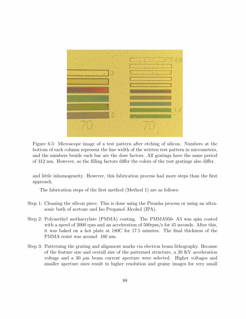
Figure 6.5: Microscope image of a test pattern after etching of silicon. Numbers at thebottom of each column represent the line width of the written test pattern in micrometers,and the numbers beside each bar are the dose factors. All gratings have the same periodof 312 nm. However, as the filling factors differ the colors of the test gratings also differ.
and little inhomogeneity. However, this fabrication process had more steps than the firstapproach.
The fabrication steps of the first method (Method 1) are as follows:
Step 1: Cleaning the silicon piece. This is done using the Piranha process or using an ultra-sonic bath of acetone and Iso Propanol Alcohol (IPA).
Step 2: Polymethyl methacrylate (PMMA) coating. The PMMA950- A3 was spin coatedwith a speed of 2000 rpm and an acceleration of 500rpm/s for 45 seconds. After this,it was baked on a hot plate at 180C for 17.5 minutes. The final thickness of thePMMA resist was around 160 nm.
Step 3: Patterning the grating and alignment marks via electron beam lithography. Becauseof the feature size and overall size of the patterned structure, a 20 KV accelerationvoltage and a 30 µm beam current aperture were selected. Higher voltages andsmaller aperture sizes result in higher resolution and grainy images for very small
88

Figure 6.6: Microscope images of fabricated gratings with period of 312 nm with (a) non-uniform filing factor of 0.3 at the middle and 0.15 at the end points, (b) uniform fillingfactor of 0.5, and (c) uniform filling factor of 0.3. The total length of each grating is 1cm, but only 5 mm of each is shown in each image. The inset in (a) shows the focusedimage at the middle and two end points.
apertures. On the other hand, lower voltages and larger aperture sizes result in lessheating damage and charge up, and smoother images.
Step 4: PMMA developing. The PMMA was developed for 30 sec in a mixture of methyl-isobutylketone (MIBK) and IPA with a ratio of 1:3 followed by dipping in IPA for30 sec.
Step 5: Deposition. Depositing 20-30 nm of Aluminum or Aluminum oxide Al2O3 using anE-beam evaporating system.
Step 6: Liftoff. For the liftoff, the sample was put in remover PG for 24 hours.
Step 7: Etching. The silicon was dry etched into the grating using aluminum or Al2O3 as amask, using a mixed gas of SF6 and C4F8 in an ICP-RIE system (Oxford Plasmalab100 ICP380 Etcher).
Step 8: Mask removing. The aluminium mask was removed by putting it in aluminiumetchant for 6-7 minutes. The Al2O3 mask was kept on the sample since it does notaffect the electrical response of the grating significantly.
The process flow is shown in Fig. 6.3(a). The grating with a period of 1µm, depth of1µm and filling factor of around 0.3, fabricated with this method is shown in Fig. 6.4. Thegrating has many defects and is not uniform.
89

Figure 6.7: SEM image of the first fabricated grating at (a) the middle and at (b) the endpoint. The silicon teeth, dSi, are 91.5 nm wide at the middle of the grating and 45 − 60nm at its end. A microscope image of this grating is shown in Fig. 6.6
The steps involved in the second approach (Method 2) used for grating fabricationare given below. There is a brief discussion of each step and some of the practical issuesinvolved in each step are pointed out.
Step 1: Cleaning the silicon piece. Done using the Piranha process.
Step 2: Depositing 20-30 nm of Aluminum. Accomplished using a sputtering system.
Step 3: PMMA coating. The PMMA was spun to a thickness of approximately 160 nm andbaked at 180C for 17.5 minutes on the hot plate.
Step 4: Grating pattern written with 20 KV acceleration voltage and 30 um beam currentaperture. Choosing a higher voltage and smaller aperture size results in better reso-lution, at the cost of slower scanning speed. Since the area of the structure is large,a 20 KV and 30 um aperture were chosen and resulted in both acceptable resolutionand patterning time.
The developed pattern is wider than the scanned pattern due to proximity-effectphenomena. Therefore, before patterning the main grating, a test pattern consistingof small gratings with different line widths and dose factors was written on the sample.Figure 6.5 shows a microscope image of a test pattern after the etching of silicon. Allthe gratings have the same period of 312 nm; however, the colors differ due to thedifferent filling factors of the gratings. Writing a pattern with a higher dose results
90

Figure 6.8: SEM image of a grating sample for which the fabrication went wrong becausethe PMMA residue was not fully removed after MIBK development.
in a grating with a smaller filling factor. For gratings with filling factors between0.25 and 0.35, the color varies from blue to green. The color changes to orange whenthe filling factor decreases to around 0.15.
After Scanning electron microscope (SEM) imaging on a developed sample, the rightwidth and dose was selected for the main structure. Since a small change in temper-ature and PMMA thickness will change the final result, it is better to do the dosetest on part of the main sample, then pattern the whole grating on it later, ratherthan conducting of doing the dose test on a separate test piece.
Electron beam focusing, with aperture stigmation and write field alignments, wasperformed at a point near to the center of the grating. The grating is 1 cm long.Therefore, close to the two ends of the grating, the electron beam loses its focus.Figure 6.6(a) shows a microscope image of the center and two end points of thefirst fabricated grating. The silicon teeth at the center of the grating are 92 nmwide.However, the width gradually changes further away from the center, becoming∼60 nm at each end (see Fig. 6.7). To solve this issue a larger silicon piece wasselected. This, allowed for the use of a clip on either side to hold the sample, ratherthan having it held by only one clip at the center. The resulting gratings are depictedin Fig. 6.6(b) and (c). The color of the grating indicates its uniformity along thewhole structure.
91

Figure 6.9: SEM images of aluminum mask (a) before silicon etching, (b) after siliconetching but before mask removal, and (c) a zoomed-out view of (b). The rough light linesare the edges of the etched silicon teeth underneath the thin aluminum layer.
Step 5: Developing the sample. Done in MIBK:IPA 1:3 for 30s followed by 30s rinsing inIPA.
Step 6: Etching 10 nm of PMMA. This was completed, using 5 second oxygen plasma etching,to remove possible unwanted PMMA residue remaining after developing. Figure 6.8shows the effect of remaining PMMA residues after silicon dry etching on a finalgrating. After development, the PMMA layer acts as an etching mask for the nextstep.
Step 7: Through-etching of the aluminum layer. Using ICP-RIE with the gas mixture ofCl2 and BCl3. The etching process takes only 5 seconds. Therefore, a pre-processwith the same temperature and gas flows, should be run first for a few minutes tostabilize the chamber temperature and the gas inside the chamber. This pre-process,reduces the typical variance of ICP-RIE processing. After the aluminum etching, theremaining PMMA mask was removed with acetone or PG remover, followed by 40second of oxygen plasma ashing. The aluminum layer acts as a hard mask duringthe silicon dry etching process.
Step 8: Etching of silicon using ICP-RIE with a gas mixture of C4F8 (passivation gas) andSF6 (etchant gas). To obtain high anisotropy and near zero undercutting, the platenRF bias power was set to 30W, whereas the ICP RF power was set at the lowestpossible value that can generate stable plasma but keep the plasma density low. Thetemperature was also set at T=0. This low temperature slows down the chemicalreactions that produce isotropic etching. The flow rates of the C4F8 and SF6 gas werefirst set equally (15 sccm). However, the side walls were not completely straight, and
92

Figure 6.10: SEM images of two gratings with dSi ' 132nm (pictures on the right) anddSi ' 92nm (pictures on the left), at three stages of the fabrication process: (a) the PMMAmask (after step 5 of the fabrication process described in the text); (b) the aluminium mask(after step 7), (c) the final fabricated grating.
93

Figure 6.11: Schematic illustration of the graphene transfer procedure.
there was lateral etching and significant undercutting. Figures 6.9(a) and (b) showa grating before and after silicon etching, respectively. In Fig. 6.9(b) the aluminiummask has not been removed. The light lines represent the edges of the etched siliconteeth underneath the aluminium layer. Figure 6.9(c) shows part of the sample wherea couple of aluminium strips are peeled away and the etched silicon layer becomesvisible.
In the next run, to improve the anisotropy of the etching profile, the flow rate of theC4F8 gas was increased to 25 sccm while keeping the flow rate of the SF6 at 15 sccm.This change achieved better anisotropy and almost zero undercut. The etching ratewas around 0.4 nm/s. Figure 6.10 shows the PMMA mask, the aluminium mask, andthe silicon grating after removing the aluminium layer for two gratings with differentsilicon teeth widths. Comparing the width of the aluminium strips in Fig. 6.10(a)with the width of the silicon tooth in Fig. 6.10(b) shows that an undercut of lessthan 3 nm was achieved.
Step 9: Removing the aluminium mask. The sample was immersed in the aluminum etchantsolution for 6 to 7 minutes.
6.2 Transfer of the graphene layer and fabrication of
the DC bias contacts
Mass fabrication of large-area uniform monolayer graphene is achieved by CVD. In thisproject, as a graphene layer with a length of 1 cm is needed, PMMA coated CVD grapheneis used. Figure 6.11 schematically illustrates the graphene transfer procedure. The graphene
94

Figure 6.12: Photos of transferred graphene layers locate on top of gratings. In (a) and (b),graphene layers transferred successfully with no wrinkles or bubbles. Figure (c) shows anexample of unsuccessful transfer of graphene with some air bubbles trapped underneath.
should be fully wetted, before being dipped very slowly into distilled water; if it is nottwill roll up or even fold. Therefore, a few droplets of IPA are placed on a spongy fabriclayer underneath the graphene piece to be absorbed.
The PMMA-coated graphene film was floated on the water surface. It should remainthere for around 2 hours to ensure that water is in contact with the complete undersurfaceof the film and not separated from it by air bubbles trapped underneath the graphene(Fig. 6.11(b)). The PMMA layer makes the graphene layer visible. With the graphenefloating on the waters surface, the sample was placed beneath it at an inclined angle, andthen gently lifted to come into contact with the graphene sheet. Further gentle pullingbrought the substrate from the water, with the graphene layer resisting smoothly on it. Thegraphene layer thus lies on the substrate, with some excess water that is washed away witha few droplets of IPA added on top of the substrate. The water is replaced with IPA sincethe latter evaporates and dries faster. At this point, any air bubbles remaining underneaththe graphene sheet can be removed by adding more IPA and tilting the substrate to oneside. While the graphene film was still wet, the substrate was inclined from side to sidein all directions to help the graphene sheet move across the substrate and locate on topof the grating. This procedure should be done as gently as possible to reduce tearing andwinkles on the graphene film. Then, the graphene was put aside and left to dry naturallyfor around 30 minutes. Figure 6.12(a) and (b) shows photos of two successfully transferredgraphene layers with no wrinkles and bubbles. In contrast, Figure 6.12(c) shows an exampleof unsuccessful transferring of graphene with a few air bubbles trapped underneath.
After 30 minutes, the sample was baked on a hot plate for 20 minutes at 60◦, then 20
95

Figure 6.13: Defects in graphene after transfer on to the silicon substrate.
minutes at 100◦-120◦, followed by 30 minutes at 200◦, allowing the PMMA to reflow as itwas baked. This last part is essential to increase the adhesion between the graphene andthe substrate. Graphene follows the surface roughness of the underlying copper during thegrowth process. Therefore, the PMMA coated graphene film is wavy and rough and sodoes not lie flat on the substrate surface. Baking the PMMA at 200 allows it to reflow andslightly stretches and flattens the graphene, as shown in the inset of Fig. 6.11(c) [127,128].Once the sample has cooled, the PMMA is removed by acetone.
Before removing the PMMA layer the graphene was investigated to check for any cracksor tears specially on the grating (See Fig. 6.13). If any cracks or tears were located onthe grating then the sample was cleaned and a new graphene sheet transferred onto it.Samples without cracks or tears were ready for the next step: fabricating the DC biasingstructure.
The DC biasing structure consists of three layers: 1) drain and source contacts whichare connected to the graphene layer through ohmic contacts, 2) an insulator layer coveringthe graphene layer, and 3) the top gate layer. The source, drain and gate are extended andconnected to the large rectangular metallic pads where the connections to the DC biasingboard are made.
Before fabricating the drain and source contacts the graphene was patterned usingoptical lithography with positive photo resist AZ p4620. The AZ p4620 was used as amask for removing uncovered graphene area, using oxygen plasma ashing for 20 seconds atlow temperature (descum process ). This was followed by removing the photo resist maskusing either heated acetone or acetone at room temperature for 24 hours, or sometimes,
96

Figure 6.14: Graphene delamination after strong liquid pressure force applied with pipette.
both. The adhesion of photoresist to graphene is stronger than the adhesion of graphene tothe substrate, especially after the plasma treatment. Thus, the graphene delaminates whenthe photo resist is removed using ultrasound or pipette to apply strong liquid pressure (seeFig. 6.14).
The residual photoresist will dope graphene, causing major problems for fabricatinggraphene devices [129]. The photoresist residue after photolithography is more than theresidue after EBL, leading to weak device performance [130, 131]. An experiment in [132]showed that photoresist residue can be effectively removed by a ethyl-2-pyrrolidone basedremover.
The fabrication of each layer of the DC-biasing structure consisted of the followingsteps:
Step 1: Spin coating of the negative photo resist ma-N 1410 with a speed of 3000 rpm andacceleration of 500 rpm/s for 60 seconds. The sample was then baked on a hot plateat 110◦ for 90 seconds. The resulting thickness of the photo resist was around 950nm.
Step 2: Optical lithography using chrome photomask. The resist was exposed to UV lightwith an intensity of 350 mW/cm2 at a wavelength of 365 nm for 35 seconds. Theexposure time value was determined using dummy samples to achieve the correctdimensions and desired resist sidewall profile. The longer the samples were exposedto radiation, the thinner the lines were. For example, for a line width of 80 µm onthe mask, an exposure time between 35 to 40 seconds resulted in a line width of 76
97

Figure 6.15: Optical microscope image of sample after ma-N 1410 resist developed in ma-D 533/S for (a) 50 seconds (no undercut) and (b) 2 minutes (with undercut). The lightbrown region is where exposed resist remains, while the yellow region is the silicon surfaceafter removal of unexposed resist. The band surrounding the yellow region in Figure (b)indicates an undercut of about 3 µm.
to 80 µm after development. On the other hand, with a negative resist, less exposuremeans more developer attack, leading to more undercut. Therefore, considering allof these factors, an exposure time of 35 second was selected.
Step 3: Developing the sample in ma-D 533/S developer. In the first experiment, the samplewas developed until the unexposed photo resist part dissolved completely, which tookaround 50 seconds. However, this time was not sufficient to achieve a good undercutprofile (see Fig. 6.15(a)), a key element for a good lift-off result. Therefore, thedeveloping time was increased to two minutes. The resulting undercut is shown inFig. 6.15(b)
Step 4 :Deposition of thin film materials using an electron beam evaporation system. Thedeposited layers are as follows:
layer 1: 10 nm of chrome or titanium and 60 nm of gold;
layer 2: 75 nm of Al2O3;
layer 3: 10 nm of chrome and 80 nm of aluminum.
The titanium and chrome layers are used to increase the film’s adhesion to the sub-strate.
Step 5: Lift-off. The goal of this crucial process is to wash away the photoresist in a solvent,together with the material deposited on its top. After the lift-off, only material in
98

Figure 6.16: Fabrication flows for (a) patterning of graphene layer, (b) fabricating drainand source contacts on the graphene, (c) adding insulator layer and (d) fabricating topgate contact. For some steps, an optical microscope image of a fabricated sample has beenadded.
99

Figure 6.17: Fabrication flow for shadow mask. For some steps, an optical microscopeimage of a fabricated sample has been added.
direct contact with the substrate should remain. In some cases, unwanted smallflakes of the metal layer adhere so well to the remaining parts that clean lift-off doesnot occur. In these cases, the application of small force with ultrasound or a pipetteremoves the unwanted flakes.
The main difficulty arises from the fact that the bonding of the graphene to thesubstrate is based on weak Van Der Waals forces. The low adhesion of graphene tothe substrate prevents the facilitation of the lift-off process using ultrasound. Theultrasonic force will remove not only the photo resist and the material on top but alsothe material deposited on the graphene, potentially damaging the graphene as well.The best that can be done is to put the sample in the solvent after the deposition
100

Figure 6.18: Fabricated shadowmask.
Figure 6.19: Silicon waveguide with a supporting block attached to it.
until the material layer on top of the photo resist is cracked and peels off from thesubstrate. Then, with the use of liquid pressure from a pipette, the lift-off processcan be completed.
Acetone and remover PG can be used as solvents for the photo resist. However, thegraphene layer interacts with remover PG and starts to detach and curl back on itself.Therefore, for the first layer, when the graphene layer had not yet been covered, thesample was put in the acetone for 24 hours, and for the second and third layers, theheated PG remover was used.
During the lift-off process, particles of metal may be redeposited on the surface,contaminating the sample at random locations. To prevent this, and to help thelift-off process, parts unnecessary to the deposition were covered and exposure of thecontacts area and surround was minimized.
a = 125µm, b = 620µm, tg = 540nm, md = 0.28 The process flow for the fabricationof the DC biasing structure is shown in Fig. 6.16. For some steps, an optical microscope
101
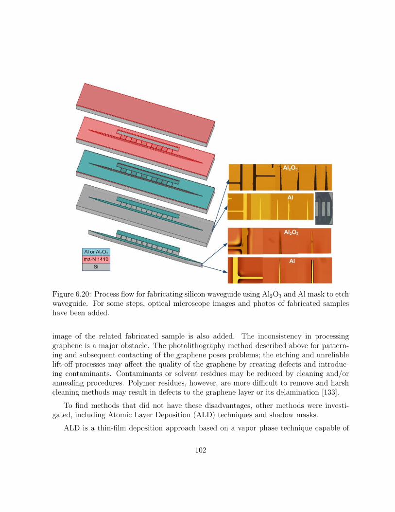
Figure 6.20: Process flow for fabricating silicon waveguide using Al2O3 and Al mask to etchwaveguide. For some steps, optical microscope images and photos of fabricated sampleshave been added.
image of the related fabricated sample is also added. The inconsistency in processinggraphene is a major obstacle. The photolithography method described above for pattern-ing and subsequent contacting of the graphene poses problems; the etching and unreliablelift-off processes may affect the quality of the graphene by creating defects and introduc-ing contaminants. Contaminants or solvent residues may be reduced by cleaning and/orannealing procedures. Polymer residues, however, are more difficult to remove and harshcleaning methods may result in defects to the graphene layer or its delamination [133].
To find methods that did not have these disadvantages, other methods were investi-gated, including Atomic Layer Deposition (ALD) techniques and shadow masks.
ALD is a thin-film deposition approach based on a vapor phase technique capable of
102

Figure 6.21: Process flow for fabricating silicon waveguide using AZ P4620 mask to etchwaveguide. For some steps, optical microscope images and photos of fabricated sampleshave been added.
depositing thin films one atomic layer at a time. ALD is based on sequential, self-limitingreactions and so offers exceptional conformality. With these advantages, along with itscapability to produce tunable film composition, ALD has emerged as a powerful tool formany applications in microelectronics.
There are two main approches for patterning ALD-grown films have been used in theliterature: (i) patterning based on lithography and lift-off or etching; and (ii) area-selectiveALD by area-deactivation or area- activation. There has been much interest in patterningby area-selective approaches since they can eliminate compatibility issues associated withthe use of solvents, etchants, or resist films when working with sensitive materials. TheALD patterned films are superior to sputtered or evaporated films in continuity, smooth-ness, conformality, and minimum- feature size. The low deposition temperature preventsdamage to the photoresist, such as from significant outgassing or hardbaking of resist layersunderneath.
ALD of thin films on graphene is, however, a much more complex task due to thelack of out-of-plane bonds and surface hydrophobicity of the graphene [134]. There areno reactive adsorption sites on the perfect graphene surface. However, boundary regions,wrinkles and defects, typical in CVD graphene, are nucleation centers for ALD films.
103

Figure 6.22: SEM image of the tip of the waveguide. Photoresist layer did not adhereproperly to the substrate, causing lateral etching through the gap under the resist.
Thus, the uniform deposition of ALD film on graphene without any surface preparationtechniques is impossible. Different techniques to initialize ALD growth on graphene havebeen investigated in the literature. These techniques include the use of different types ofseed layers [135–137], ozone and plasma treatments to create functional groups [138, 139],and enhance nucleation by tuning the underlying substrate [140]. Research is ongoingto develop a method that does not damage the graphene, and/or degrade the electricalproperties of graphene such as its carrier mobilities.
Paradoxically, the difficulties of growing ALD on graphene can be exploited in thefabrication of graphene and graphite-based structures through self-aligned ALD. In thistechnique, the material is selectively deposited on the materials where it is desired, elimi-nating the nano-scale alignment difficulties and multistep lithography processes.
Another method for fabricating contacts on graphene is to replace the patterned pho-toresist layer with a shadow mask. A shadow mask is a thin sheet with pattern featuresetched completely through it. After being positioned in intimate contact with the sub-strate, it is placed into the electron beam evaporation system. The thin film material isdeposited through the mask directly on the substrate. This simplified process eliminatesseveral steps associated with the photolithography and lift-off processes without contam-inants or residues affecting the quality of the graphene. However, shadow masks are notgood for high-resolution applications. Furthermore, shadow mask alignment is more dif-ficult than the alignment in photolithography, and it is not as accurate. In this thesis,200 µm silicon was employed to fabricate a shadow mask, using the fabrication procedureillustrated in Fig 6.17. and described below:
104

Figure 6.23: (a) Remaining solvent in the resist out-gassed after exposure and filled exposedarea with micro-cavities. (b) Effect of a bubble on a sample after photo resist development.(c) Bubble created during dry etching. (d) Effect of a bubble created during dry etchingon a sample after etching.
Step 1: Positive photo resist AZ P4620 was spun to a thickness of approximately 10 um andbaked at 115◦C for 90 seconds.
Step 2: Optical lithography was carried out using the same chrome photomask as the oneused in the previous method to pattern contacts on the negative photoresist.
Step 3: The photoresist was developed in AZ developer 1:4 for around 2 minutes 20 seconds,followed by 1 minute rinsing in water.
Step 4: 100 nm Al2O3 was deposited using the electron beam evaporator system.
Step 5: The sample was soaked in the PG remover to accomplish the lift-off process.
105

Figure 6.24: Microscope image of two AZ-P4620 patterns with different exposure times:(a) 75 seconds, and (b) 58.4 seconds. The black bond around the pattern indicates theangled sidewalls.
Step 6: Through etching of 200 um silicon was performed using the Al2O3 layer as a mask,in the Oxford Plasmalab 100 ICP380 system, using the Bosch process. Al2O3 is achemically inert material and gives appropriate selectivity.
The fabricated shadow mask is shown in Fig. 6.18. Rough alignment under the opticalmicroscope led to a misalignment of around 100 µm. The alignment precision can beimproved to 5-10 µm by using a shadow-mask aligner equipped with a three-axis micropo-sitioner and 1 rotation axis and 2 tilt axes. At the time of measurement, this system wasnot available.
6.3 Fabrication of the silicon waveguide
The last stage is to etch the silicon substrate into the silicon waveguide and its attachedsupporting block (see Fig. 6.19). The etch thickness is around 300 um. Therefore, thechallenges of this stage are in controlling the lateral etching so as to fabricate straight wallwaveguides, and in using an etch mask that can resist the long etching process. For thelatter, either a mask with very high selectivity or a very thin mask with typical selectivitycan be used. Therefore, two different types of mask materials were tested for the etching
106

Figure 6.25: Profile pattern of 11 µm AZ P4620 photoresist (a) before and (b) after postbake at 110◦C for 5 minutes. Insets are corresponding microscope images.
process: soft masks made of thick layers of the positive photo resist AZ P4620, and hardmasks made of Al2O3 and Al.
The selectivity of the hard masks is very high [141]. Any reactions Al2O3 and Al havewith the etchant gas SF6 are too small to perceive; attempts to measure any changes inthe thickness of hard masks before and after etching with filmetrics and profilometer wereunsuccessful. However, based on the experiments done, it is possible to say the selectivityis greater than 1000 and 5000 for aluminum and aluminum oxide, respectively.
Using a hard mask required additional deposition and lift-off steps, as depicted in Fig.6.20. The hard mask was fabricated by coating the sample with 950 nm of negative photoresist ma-N 1410 followed by patterning the photo resist via optical lithography. Then,
107

Figure 6.26: SEM image of silicon waveguide etched by (a) standard Busch process with apatterned AZ-P4620 mask, and (b) Busch process with longer passivation time step, withthe same AZ-P4620 mask, postbaked at 110◦ for 5 minutes.
100 nm Al2O3 or Al were deposited by electron beam evaporation. The lift-off processwas accomplished in PG remover heated to 80◦C (see Fig. 6.20). A very clean lift-off isrequired, as any small flakes of material remaining after the lift-off lead to rippling alongthe edge of the etched waveguide.
The patterned photo resist layer can also be used as an etch mask. For this purpose,the thick photo resist AZ P4620 was used. Figure 6.21 illustrates the fabrication steps.The details of each step are explained below. The surface preparation before coating is anessential step for proper adhesion. Weak resist adhesion could result in the resist patternpeeling off after development, or unwanted lateral etching through the gap under the resist(Fig. 6.22). Surface moisture is a major factor that degrades resist adhesion. Therefore,surface preparation consists of dehydration through baking to remove surface moisturethen the addition of an adhesion-promoter, hexamethyl disilizane (HMDS). The substratedehydration and vapor deposition of HMDS were performed in a YES HMDS prime oven.
The selectivity of the photo resist is around 20 to 30. Therefore, the etching of 300
108

Figure 6.27: (a) Sample before etching mounted on aluminum-oxide-coated wafer. (b)Fabricated sample.
um silicon requires a photo resist thicker than 15 um. For this resist, the maximumthickness of the single coat is around 17 µm, and the required thickness can be achievedby a single-coating. However, the solvent content of the resist is vaporized more rapidlyand more efficiently by successive spinning and baking processes. Therefore, a thick resistof around 24 µm was achieved by spinning the photo resist, then baking it on a hot plate,then repeating the spin-bake cycle. For both spinning processes, the photoresist was firstspread at a speed of 500 RPM for 10 seconds, followed by a spin at a speed of 2000 RPM for25 seconds. Different durations and temperatures were tested for the two baking processes.
AZ P4620 is a DNQ-novolac photo resist, consisting of novolac resin, an organic sol-vent, and diazonaphtoquinone (DNQ) photoactive compounds. The excess solvent shouldbe removed by softbaking after the photo resist coating. If the softbake is short and/or thetemperatures are too low, the dork erosion will increase, and the high remaining solventconcentration may cause bubbles during exposure or dry etching (see Fig. 6.23). Thesolvent will out gas and the resist layer will be filled with micro cavities (see Fig. 6.23(a)).On the other hand, high temperatures or long baking times will thermally decompose asignificant amount of the photo active compound, lowering the development rate signifi-
109

Figure 6.28: Measurement setup.
cantly [].
The best result was achieved with a soft bake temperature and time of 110◦ and 80seconds for the first layer and 115◦ and 10 minutes for the second layer. Lower temperaturesresulted in bubbling, and higher temperatures resulted in very difficult or even impossibledevelopment.
A certain water content in the DNQ-based resist is required during exposure to attaina high development rate []. Softbaking, however, makes the resist film almost water-free.Thus, the required water is gradually drawn from the air into the resist film. Therefore,a delay between baking and exposure is necessary for rehydration of the photoresist film.This time depends on the photoresist’s thickness, air temperature and humidity.
After more than 3 hours rehydration time, the photoresist was exposed to a UV lightwavelength of 405 nm with an intensity of 25 mW/cm2 for 58.4 seconds. Exposure time wasadjusted to achieve steep resist sidewalls. Exposure doses that are too high cause undesiredexposure by scattering, diffraction and reflection. As a result, too much of the resist isdissolved during development. On the other hand, the resist is not developed successfully
110

Figure 6.29: Simulated S-parameters of silicon image waveguide with length of lsi = 20mm, width of wsi = 125µm, thickness of hsi = 300µm and taper length of ltaper = 5.5mm,with and without attached supporting block.
with a low-exposure dose. Figure 6.24 shows microscope images of the developed two-layerpatterned photoresists with different exposure times of 75 seconds and 58.4 seconds. Ascan be seen, the shorter exposure time results in straighter sidewalls.
As discussed above, achieving straight vertical walls with thick photo resist is difficult.Another method is to create a thinner photoresist layer, but to also improve the selectivityof the mask by hardening the photoresist with post baking after development. A post-development bake (or ”hard bake”) of the photoresist pattern is a common method forstabilizing a printed pattern so that it will withstand the harsh environments of etching.This final bake step removes residual solvent, water, and gasses and improves adhesion ofthe photoresist to the substrate and its resistance to RIE etches. Post baking increasedthe selectivity of the photo resist to around 100.
The photoresist was spun to a thickness of approximately 11 um, then cooked at 110for 90 seconds. After more than 3 hours delay for rehydration, the coated photo resist wasexposed to UV light for 29.2 seconds and developed in 4:1 diluted AZ 400 for 2:40 minutes.Then, it was baked for 5 minutes on a hot plate at 110◦C. Figure 6.25 shows both profiles(measured by the Bruker profilometer) and microscope images of the developed patternedphotoresists before and after the post bake (inset). As depicted in this figure, the profilepattern is a little distorted due to thermal reflow.
The ultimate purpose of the hard bake is full removal of the solvent. However, since the
111

Figure 6.30: Measured S-parameters of fabricated silicon waveguide with no grating andgraphene layer.
diffusion rate of the solvent is extremely low in solid photoresist, in order to achieve fullremoval for a thick photo resist the photoresist is baked at temperatures higher than theglass transition temperature of the resin. The resist is thus transformed from a glassy stateinto a soft rubbery state and starts flowing. In this semi-liquid state, the diffusion rate issignificantly improved. Therefore, hard baking is usually done at or slightly above the glasstransition temperature, so the flow of the resist degrades the resist profile significantly.
Thermal deformation of positive photoresist patterns during high temperature treat-ments is significantly reduced by deep UV curing of the resist surface to form a hard outershell. In this method, the outer layer of the photoresist image is exposed to UV radiationin the range of 200-320 nm. The novolak resin in the photoresist is highly absorptive atthis wavelength band. Therefore, the short wavelength UV lights penetrate only about100 nm into the resist film. The thin cured layer allows hard baking of the photo resistat temperatures up to 200◦C without any deformation. After deep UV curing, stripperscannot remove the resist and O2 plasma etching is required to completely remove it.
112

Figure 6.31: DC bias circuit.
The novolak-based AZ P4620 resist has a glass transition temperature of around 125◦C.Since there was no access for this thesis to a deep-UV cure system, temperatures smallerthan the glass- transition temperature were tested for hard baking. A 110◦C and 5 min bakeresulted in only a small distortion of the pattern profile and sidewalls, and the photoresistwas hardened enough to withstand etching of 300 µm silicon.
It is better to shorten the delay between hard baking and etching so as to preventrehydration of the resist. As mentioned in the beginning of the chapter, the Bosch processon an ICP-RIE system was used to fabricate rectangular dielectric waveguides. The etchrate depends on the amount of exposed silicon area on the wafer. A larger exposed arealeads to a lower etch rate. Therefore, the samples were mounted on aluminium-oxide-coated wafers before being put inside the ICP-RIE system (for etching)(Fig. 6.27(a)).
The Bosch recipe parameters were modified to 90◦ sidewalls. Figure 6.26(a) showsan SEM image of the etched waveguide cross section etched by the standard Bosch siliconetching process in Oxford Plasmalab System 100 ICP380 DRIE at a temperature of T=0◦C.As can be seen, the sidewall angle is less than 90◦ and the etch rate in the horizontaldirection is not zero. Therefore, the passivation step time was increased from 5 secondsto 7 seconds while keeping all other parameters unchanged. Figure 6.26(b) shows a SEMimage of the etched waveguide cross section fabricated by the above mentioned modificationwhich resulted in perfectly vertical sidewalls. For both figures 6.26 (a) and (b), the one-layer AZ-P4620 masks were fabricated with the same recipe except that for Fig. 6.26(b)the mask was hard-baked after the development.
A resist strip is the final operation after the etching process is completed. The etchedsilicon waveguides were dipped in heated PG remover for one hour. If that did not removethe resist layer, it was etched using two minutes of oxygen plasma ashing at 180 degrees.Figure 6.27(b) shows the image of the fabricated sample. The next step is to connect thebiasing voltage and conduct measurements.
113

140 145 150 155 160 165 170
f (GHz)
-25
-20
-15
-10
-5
0
S1
1 a
nd
S2
1 (
dB
)
S11
: no pcb board
S21
: no pcb board
S11
: VGS
=0 , VDS
=0
S21
: VGS
=0 , VDS
=0
S11
: VGS
=3V , VDS
=30V
S21
: VGS
=3V , VDS
=30V
Figure 6.32: Measured S-parameters of fabricated graphene TWA over the frequency rangeof 140-170 GHz.
6.4 Measurement results
The fabricated structures were measured using a 1-50 GHz Agilent network analyzer con-nected to two OML millimeter-wave frequency extension modules, covering the frequencyrange of 110-170 GHz (see Fig. 6.28). The frequency extension modules were placed onmicro positioning stages, with 4-axis degrees of freedom: x, y, z, and φ.
A metallic fixture, manufactured by Computer Numerical Control (CNC) machinery,was used to hold the silicon waveguide. The holder acts as the ground plane of thisimage waveguide. Therefore, it should be aligned precisely with respect to the metallicwaveguide ground of the OML modules. To bring these structures into alignment, themicro positioning stages were used with the help of alignment holes and pins on the holderand waveguide flanges, respectively.
The ports of the OML modules are WR-06, standard metallic waveguides. The dielectric-to-metallic waveguide transition was realized by a tapered section of the silicon waveguideinserted into the metallic waveguide (see inset of Fig. 6.29). The tapered length wasoptimized to achieve good insertion loss. The silicon waveguide was supported from oneside by means of a silicon supporting block that connected to the waveguide by narrowbeams (Fig.6.19). Figure 6.29 shows the simulation results for a silicon waveguide with
114

140 145 150 155 160 165 170
f (GHz)
0
1
2
3
4
5In
tensity g
ain
(d
B/c
m)
Figure 6.33: Calculated intensity gain versus frequency obtained from theoretical analysisfor a TWA structure with the same dimensions as the fabricated sample with Ef = 0.3 eVand Vd = 3× 10⁵m/s.
and without a supporting block attached to it. Since the widths of the supporting beamsare very small, wbeam = 50µm, negligible power transfers to the supporting structure. Themeasurement results for the fabricated silicon waveguide with no grating and graphenelayer are shown in Fig. 6.30.
The next step is to perform measurement on the fabricated graphene TWA prototypeof with a = 125µm, b = 620µm, tg = 540nm, and md = 0.28 . The DC bias circuit isshown in Fig. 6.31. The measurements results before attaching the DC biasing printedcircuit board (PCB), after attaching the PCB but before applying the DC voltages, andafter applying the DC voltages VGS = 3V and VDS = 30V , are shown in Fig. 6.32. Afterapplying the DC voltages, the S21 increased by a value between 0 to 2.7 dB at the frequencyrange of 140-170 GHz. The fabricated graphene TWA has a maximum gain of 2.7 dB/cmat 151.5 GHz. As predicted by the theoretical analysis (see Fig. 6.33), the maximum gainis obtained close to the cutoff frequency. Figure 1.33 shows the calculated intensity gainversus frequency obtained from theoretical analysis for a graphene TWA structure withthe same dimensions as the fabricated sample, assuming Ef = 0.3 eV and Vd = 3 × 10⁵
m/s.
115

6.5 Conclusion
In this section, the procedure used to fabricate a novel integrated graphene-based travellingwave amplifier is described. This research uses newly developed silicon waveguide-basedtechnology in the THz range of frequencies and integrates it with both nanofabrication andgraphene technology. The fabrication procedure has more than ten major steps, includingEBL, graphene transfer, dry etching, optical lithography and lift off. The challenges ofeach step are described and detailed solutions provided.
Two methods for fabricating the grating structure are proposed and tested based onalready-established nanofabrication techniques. The details of the more reliable approach,which results in a uniform 1 cm long grating with nano scale dimensions, are given. Fur-thermore, two established methods for fabricating the graphene contacts are described onebased on optical lithography and the other on a shadow mask. The first method consistingof optical lithography, deposition and lift-off, is used to fabricate the prototype structures.Because of the very weak bond of graphene to the substrate and metallic contacts, theapplication of ultrasound for cleaning and lift-off often damages the graphene and the con-tacts above it. On the other hand, removing the electron and photo resist residues ongraphene is also difficult and affects the performance of the device. However, with themethod utilized a precise alignment is achieved. Thus, an alternative method which avoidsthe problems with resist residues and difficult lift-off processes, is adopted. In this method,a shadow mask is used instead of patterned photo resist masks to fabricate the contactson graphene. However, shadow mask alignment is more difficult than the alignment inphotolithography and not as accurate. The alignment technique must be improved if thismethod is to be applied for future samples.
For fabrication of the 300 m thick silicon image waveguide, two methods are discussed:hard mask and thick photoresist mask. The advantages and disadvantages of each methodare discussed and tested. Ultimately, a reliable fabrication process that yielded straightvertical walls with no lateral etching was developed.
The first fabricated prototype structure is measured using an Keysight network ana-lyzer. Measuring the s-parameters of the waveguide before and after applying the DC biasvoltages shows a maximum of 2.7 dB/cm gain for a 30 V/cm electric field at 151.5 GHz.Here, for the first time, measurements have confirmed that graphene can be used for trav-elling wave amplification. Although the amount of gain measured for this first prototypestructure is small, this work establishes a clear beginning. Room for improvement remains,and will be discussed under future work (Section 7.1).
116

Chapter 7
Conclusion
In summary, a novel solid-state TWA using graphene as a conducting layer is proposed,thoroughly studied, successfully fabricated, and characterized in this thesis. Both theo-retical and measurement results show that graphene is a good candidate for solid-statemm-wave and THz TWAs. The proposed graphene TWA is suitable for integration infuture monolithic integrated THz circuits.
In this thesis, for the first time, travelling wave amplification in graphene was exploredby developing two different models to define the conductivity for drifting charge carriersin graphene. In the first approach, a quantum mechanical model is developed to obtainthe frequency and wave number dependent conductivity of graphene with drifting chargecarriers under a non-equilibrium condition (Chapter 3). The second model used is a clas-sical hydrodynamic model (Chapter 4) derived with a relativistic fluid approach in whichthe electrons in graphene are modelled as a 2D Fermi liquid. Based on this hydrodynamicmodel, the induced current is calculated for harmonic perturbation of both stationary anduniformly moving charged carriers, and the linear conductivity is obtained.
The conductivity relations obtained from both methods show that, for a slow electro-magnetic wave with a phase velocity smaller than the drift velocity of the carriers, graphenechanges from a lossy medium to a gain medium that converts power from the DC sourceto the electromagnetic field. Although the two methods are quite different, one beingmore classical and the other more quantum mechanical, the behaviour of the conductivityfunctions with respect to the frequency and wavenumber are remarkably similar.
In Chapter 5, grating structures on silicon slab and silicon rod waveguides are designedas slow wave structures for the proposed TWA. The Floquet mode solution of the first-order space harmonic(satisfying the travelling wave amplification requirement, Vph < Vd),
117

is presented. Coupled wave analysis is used to obtain the interaction impedance and theoverall gain of the graphene TWA. The estimation of an attainable gain for an optimizedslow waveguide under reasonable bias is 10.5 dB/cm at 1 THz.
To simplify and speed up the fabrication process, the prototype structure is fabricatedfor a frequency range of 110-170 GHz. Therefore, a rod silicon waveguide with a thingrating layer on top is designed at a frequency of 150 GHz. A new approximate theoreticalmethod is developed for analyzing the hybrid space-harmonics in gratings on top of rect-angular dielectric waveguides. This method gives an explicit expression for the interactionimpedance of slow wave grating structures, which is then used to design the waveguideand the grating. To verify the proposed approximation approach, the results obtainedwith this method are compared with simulation results obtained from FEM-based ANSYSelectronics software.
The fabrication of the prototype structure consisted of fabricating three integratedmain structures: the grating, the graphene layer attached to DC bias contacts, and thesilicon waveguide. For each of these devices, reliable fabrication recipes are developed andcombined to create the first graphene TWA integrated in a mm-wave silicon waveguide.
The first fabricated sample is measured using a Keysight network analyzer. The mea-surements show a maximum gain of ∼2.7 dB/cm for a 30 V/cm electric field at 151.5 GHzand thus, both theoretical and experimental results confirm that the graphene layer canbe used for travelling wave amplification.
Future stages of this research are presented in the next section.
7.1 Future work
1) Non-linear analysis of large signal interactions with drifting plasma wave ingraphene
In the current work, only the linear response of graphene was studied. The non-linearresponses of graphene can be obtained by considering higher order terms in hydrodynamicequations. In such a method, the effect of the DC current on the non-linear conductivityof graphene could be explored.
2) Combining numerical methods with the proposed Fourier mode anal-ysis to achieve more accurate estimation of parameters such as interactionimpedance and gain.
118

In Chapter 5, an approximate analytical method was proposed to calculate the couplingfactor between the drifting space charge wave in graphene and first-order space harmonicof the slow-wave grating structure. Based on the Fourier solution approach, a recursiveformula was obtained in which the first-order space harmonic of the grating is determinedin terms of the zeroth order harmonic. For thin gratings, the corresponding mode of thestructure with no grating is a good approximation for the zeroth order harmonic. Therefore,in the proposed method, a good estimation of the waveguide mode will significantly improvethe accuracy of the solution for the first-order space harmonic. The approximate resultsare shown to be in very good agreement with the simulation results for the slab waveguidefor which an accurate analytical modal solution is available (Fig. 5.3). However, forrectangular waveguides, where there is no analytical solution, there is a discrepancy. Thisis especially true near cutoff points where the estimation of the modes obtained from theimproved Marcatili approach have the lowest accuracy (Fig. 5.24).
Therefore, to obtain more accurate results, rigorous numerical methods should be usedto obtain the field of a rectangular waveguide with no grating and then this result couldbe used in the proposed method to accurately estimate the field of the first-order spaceharmonic of the grating.
In this way the lengthy computation time required to analyze long gratings (∼ 1− 3λ)with very fine feature size (1/10000λ) could still be avoided, and much more accurateresults could be achieved.
3) Increase the graphene maximum achievable charge density and drift ve-locity
The maximum achievable value of the Fermi energy level is limited by the breakdownfield strength of the gate dielectric. For example, for SiO2 the dielectric strength is around107 V/cm [?] and thus the maximum Fermi energy level value that can be achieved isaround 300 meV (Fig. 2.4). However, with very specific dielectric materials such as ion-gel [142] and solid polymer electrolyte [143], it is possible to achieve Fermi energy levelsas high as 1-2 eV. Figure 5.5 shows that increasing the Fermi level will increase the gainsignificantly.
Another important parameter that determines the maximum achievable gain is thedrift velocity (see Fig. 5.6). The mobility, and thus the drift velocity, of graphene is verysensitive to the density of defects. Therefore, applying a better fabrication method forgraphene will result in higher gain.
4) Improving the measurement setup to perform more accurate measure-ments
119

Figure 7.1: New metallic holder with 3D printed plastic cover.
After attaching the PCB, the sample should be fixed on the holder; otherwise, it willnot sit flat on the ground surface. In the setup used to obtain the measurement results inthis thesis, the sample was held in place by needle-sharp tweezers. This was not efficientas the sample moved after each measurement and had to be realigned until the maximumS21 value was obtained.
Therefore, a new metallic holder with a 3D printed plastic cover was manufactured (seeFig. 7.1). With this setup, the waveguide can be aligned once and stay fixed in place withthe help of the plastic cover, while the DC biasing voltages are swept during measurements.
5) Fabricating a graphene-based structure for a higher range of frequencies
The proposed graphene-based TWA was demonstrated up to 170 GHz. The design ofthe structure should be refined to perform at higher frequencies.
6) Fabricating a THz beam amplifier with planar 2D structure
Future work could explore other types of graphene TWAs (see Fig. 7.2). In thisconfiguration, the graphene sheet is placed on top of a periodic grating structure. Theslow wave in the periodic grating is excited by the graphene SPP wave. The slow wave isamplified and fed to the grating antenna through a tapered grating. Fabricating such astructure will be easier than the architecture proposed in this thesis.
In Chapter 2, it was shown that the propagation constant of the SPP waves can beas large as 50 times the free space wavenumber (see Fig. 2.7). However, the propagationconstant of the slow wave in the grating structure of the TWA is significantly larger thanthe propagation constant of the SPP wave in graphene. Therefore, a coupling structure
120

Figure 7.2: Proposed alternative graphene TWA.
should be designed to gradually match the SPP wave to the slow wave of the grating. Theamplification should be large enough to compensate for the coupling loss. The developmentof such a structure will allow for the amplification of THz beams for a wide range ofapplications, such as THz spectroscopy and imaging applications.
121

APPENDICES
122

Appendix A
Tight-binding approach
In a periodic lattice structure the wave function of electrons should satisfy Blochs theorem
TaiΨ = eik.aiΨ (A.1)
where Taiis a is the translation operator along the lattice vector ai (see Fig. 2.1). The
wave function is commonly defined as a linear combination of plane waves. In this case, wecannot easily relate the wavefunction to the atomic orbitals. Also the scale of computationis large since we have to use the large number of plane waves to reach desired accuracy.Another wave function form which is used in the tight binding method is based on theatomic orbitals in the unit cell [77]. Therefore, the tight binding Bloch function is definedas [77]
Φj (k, r) =1√N
N∑R
eik.Rφj (r−R) (j = 1, ..., n), (A.2)
where R is the position of the atoms in the lattice, φj is the jth atomic orbital in the unitcell and N is the total number of unit cells. Therefore, we just have n Bloch functions(n denotes the number of atomic orbitals in the unit cell). The eigenfunctions are thendetermined as the linear combination of Bloch functions [77]:
Ψj (k, r) =n∑
j′=1
Cjj′ (k) Φj′ (k, r), (A.3)
123

and the energy eigenvalues are given as [77]
Ei (k) =
∫Ψ∗iHΨidr∫Ψ∗iΨidr
=
n∑j,j′=1
Hjj′ (k)C∗ijCij′
n∑j,j′=1
Sjj′ (k)C∗ijCij′, (A.4)
where H is the Hamiltonian of the system. By setting a partial derivative of Ei related toC∗ij equal to zero, in order to minimize Ei, we obtain the following equation [77]:
HCi = Ei (k)SCi, Ci =
Ci1...Cin
, (A.5)
where the elements of matrices H and S, known respectively as the transfer integral matricesand overlap integral matrices, are determined as follow [77]:
Hjj′ (k) = 〈Φj|H |Φj′〉 (A.6)
Sjj′ (k) = 〈Φj | Φj′〉 (A.7)
The transfer and the overlap matrix elements are often considered as parameters, and theirvalues are determined so that the calculated band structure of the solid matches the oneobtained either experimentally or from first principles calculations. It is deduced from A.5that in order to have a nontrivial solution the following condition should be satisfied:
det [H − Ei (k)S] = 0 (A.8)
This equation is called the secular equation. By solving the secular equation for the givenk, the n eigenvalues of Ei are obtained.
A.1 Electronic structure of graphene
Carbon atoms have four valence electrons, which occupy 2s, 2px, 2py, and 2pz orbitals.In graphene the 2s orbital and two 2p orbitals are mixed with each other, forming threeσ bonds. These bonds are completely filled, thus forming a deep valance band. Theunaffected p orbital, which is perpendicular to the planer structure, leads to the formationof a half filled π band. The π energy bands are covalent bands that play the most significant
124

role in the solid state properties of graphene. Therefore, we have two Bloch functions,constructed from the atomic orbitals of two carbon atoms A and B in the unit cell:
Φj (r) =∑Rα
eik.Rαφj (r−Rα) , (α = A,B) (A.9)
where the summation is taken over the position of the A or B atoms in the structure.The Hamiltonian matrix is obtained by substituting A.9 in A.6. For diagonal elements wehave [77]:
HAA (r) = HBB (r) = 1N
∑R
∑R′eik(R−R′) 〈φ (r−R′)|H |φ (r−R)〉
= 1N
∑R=R′
ε2p + 1N
∑R=R′±ai
e±ik.ai 〈φ (r−R′)|H |φ (r−R)〉
+ (terms equal to ormore dis tan t thanR = R′ ± 2ai)= ε2p + (terms equal to ormore dis tan t thanR = R′ ± ai)
(A.10)
where ε2p is the orbital energy of the 2p level. Also for off diagonal elements HAB = H∗BAwe consider only the contribution of the nearest neighbour A and B atoms.
HAB = H∗BA = t(ejk.δ1 + ejk.δ2 + ejk.δ3) = tf(k) (A.11)
where t = 〈φA(r −R)|H |φB(r −R± a)〉 is the transfer integral, also known as the nearestneighbor-hopping energy. Similarly the overlap matrix Sij can be calculated (eq. A.7).Assuming a normalized atomic wavefunction, we have SAA = SBB = 1 and SAB = S∗BA =sf(k) , where s = 〈φA(r−R) | φB(r−R± δi)〉 is the overlap integral between the nearestA and B atoms. Therefore, the Hamiltonian, H, and overlap, S, matrices are
H =
(ε2p tf (k)
tf ∗ (k) ε2p
)(A.12)
and
S =
(1 sf (k)
sf ∗ (k) 1
)(A.13)
Substituting the above defined matrices in the secular equation (eq. A.8) and solving itfor each k the two eigenvalues E (k) are obtained as a function of k [77]:
E (k) =ε2p ± t |f (k)|1± s |f (k)|
(A.14)
125

where f (k) is defined in eq. A.11 The + sign gives the upper anti-bonding π∗ band, andthe sign gives the lower bonding π band. These two bands touch at six Dirac points.By ignoring the overlap integral between adjacent atoms orbitals and considering the nextnearest neighbour-hopping energy, t′, the energy bands are obtained as follows [3]:
E± (k) = ±t√
3 + g (k)− t′g (k)
g (k) = 2 cos(√
3kya)
+ 4 cos(√
32kya)
cos(
32kxa) (A.15)
in which a = |ai| .
126

Appendix B
Coupled-mode analysis of Floqueteigenmodes
The wave equation in the presence of an external current is
∇×∇× E− ω2µεE = −jωµJ (B.1)
Assume an external current distribution:
J = Je(x, y)e−jβz (B.2)
which will excite eigenmodes of the periodic waveguide. For a particular Floquet modeEA:
EA) = ΣmEAm(x, y)e−jβmz (B.3)
βm = β0 +m2π
dm = 0,±1,±2, · · · (B.4)
if for its first-order space harmonic β1 ' β, then this mode will be predominantly excitedand its amplitude will grow slowly. Therefore, the solution of equation B.1 can be writtenas:
E = K(z)EA (B.5)
where K(z) is a slowly varying function.By replacing E in eq. B.1 with E from eq. B.5,after some mathematical manipulation we get:
127
K ′′(z) (EA − EAz z) +K ′(z)
(∂
∂zEA − z × (∇× EA)− z∇ · EA
)= jωµJ (B.6)
The z component of the first term is zero. Multiplying eq. B.5 by E∗A and integratingover all space yields:
K ′(z)
∫ d
0
dz
∫ ∫ ∞−∞
dxdyE∗A · LA =
jωµ
∫ d
0
dz
∫ ∫ ∞−∞
dxdyE∗A · J (B.7)
where
LA =∂
∂zEA − z × (∇× EA)− z∇ · EA (B.8)
In deriving eq. B.7, K ′(z) variation over one period of d is assumed to be negligible.Therefore, it is pulled out of the integral. We assume that the Floquet mode EA and thecurrent J are nearly phase matched through the first-order space harmonic.
∆β1 = β − β0 −2π
d≈ 0 (B.9)
Therefore, we can assume that the function e∓j∆β1z is nearly constant over the periodof d. By this assumption, we can rewrite eq. B.7 as follows [73]:
K ′(z)
∫ d
0
dz
∫ ∫ ∞−∞
dxdyE∗A · LA =
jωµe−j∆β1z∫ d
0
dzej∆β1z∫ ∫ ∞
−∞dxdyE∗A · J (B.10)
For the left hand integral of eq. B.10, after some mathematical interpolation andsubstituting the magnetic field from the Maxwell’s equation, we get:
128

∫ d
0
∫ ∫ ∞−∞
dzdxdyE∗A · LA = −jωµ∫ d
0
∫ ∫ ∞−∞
dzdxdyz · (E∗A ×HA + EA ×H∗A)
= −4jωµdPA (B.11)
Here PA is the total average z-directed power carried by mode EA. For very thingratings, we can assume that most of the power is carried by the fundamental harmonicand PA ' PA0.
The Floquet expansion of the EA mode (eq. B.3) is substituted in the right handintegral of eq. B.10 to perform the z integration. Only the term with the first-order spaceharmonic does not vanish in the z integration. Therefore, eq. B.10 yields [73]:
K ′(z) = −e−j∆β1z
4PA0
∫ ∞−∞
∫ ∞−∞
dxdyEA1
∗(x, y) · Je(x, y) (B.12)
K(z) = −j e−j∆β1z
4PA0∆β1
∫ ∞−∞
∫ ∞−∞
dxdyE∗A1(x, y) · Je(x, y) (B.13)
Substituting K(z) in eq. B.5 for the particular synchronous space harmonic field,E1(x, z), we find
E1(x, z) =−j
4PA0∆β1
EA1(x, y)e−jβz∫ ∞−∞
∫ ∞−∞
dxdyEA1
∗(x, y) · Je(x, y) (B.14)
129

Appendix C
Marcatili’s method
The electromagnetic waves propagating along a straight waveguide are classified into TE,TM or hybrid modes according to the presence or absence of the longitudinal field com-ponents Ez and Hz components. The dielectric rectangular waveguide can only supportshybrid modes with both Ez and Hz present. We consider a monochromatic wave withangular frequency ω, propagating in the z direction with a propagation constant β. In anhomogeneous region j, with the relative dielectric constant of εr = εrj = cons, it is possibleto describe the full electromagnetic fields in terms of the longitudinal field components ineach region j:
Ex =−jβzK2j
∂Ez∂x− jωµ
K2j
∂Hz
∂y(C.1a)
Ey =−jβzK2j
∂Ez∂y
+jωµ
K2j
∂Hz
∂x(C.1b)
Hx =jωε
K2j
∂Ez∂y− jβzK2j
∂Hz
∂x(C.1c)
Hy =−jωεK2j
∂Ez∂x− jβzK2j
∂Hz
∂y(C.1d)
Here, all components satisfy the reduced wave equation (here given only for Ez)
∇2tEz +K2
jEz = 0 (C.2)
130
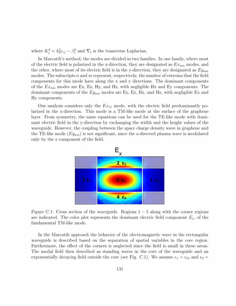
where K2j = k2
0εrj − β2z and ∇t is the transverse Laplacian.
In Marcatili’s method, the modes are divided in two families. In one family, where mostof the electric field is polarized in the x-direction, they are designated as Exnm modes, andthe other, where most of its electric field is in the y-direction, they are designated as Eynmmodes. The subscripts n andm represent, respectively, the number of extrema that the fieldcomponents for this mode have along the x and y directions. The dominant componentsof the Exnm modes are Ex, Ez, Hy, and Hz, with negligible Hx and Ey components. Thedominant components of the Eynm modes are Ey, Ez, Hx, and Hz, with negligible Ex andHy components.
Our analysis considers only the Ex11 mode, with the electric field predominantly po-larized in the x-direction. This mode is a TM-like mode at the surface of the graphenelayer. From symmetry, the same equations can be used for the TE-like mode with domi-nant electric field in the y-direction by exchanging the width and the height values of thewaveguide. However, the coupling between the space charge density wave in graphene andthe TE-like mode (Eynm) is not significant, since the z-directed plasma wave is modulatedonly by the z component of the field.
Figure C.1: Cross section of the waveguide. Regions 1 − 5 along with the corner regionsare indicated. The color plot represents the dominant electric field component Ex, of thefundamental TM-like mode.
In the Marcatili approach the behavior of the electromagnetic wave in the rectangularwaveguide is described based on the separation of spatial variables in the core region.Furthermore, the effect of the corners is neglected since the field is small in these areas.The modal field then described as standing waves in the core of the waveguide and anexponentially decaying field outside the core (see Fig. C.1). We assume ε1 = εSi and ε2 =
131

ε3 = ε4 = ε5 = εair. Hereafter, we use the symmetry conditions to reduce the calculationdomain to regions 1,2 and 3. Therefore,the longitudinal components are expressed as:
ez0 =
A2e
−γx(x−b/2) cos(kyy) x > b/2,−a/2 < y < a/2
A1 sin(kxx) cos(kyy) −b/2 < x < b/2,−a/2 < y < a/2
A3 sin(kxx)eγy(y−a/2) −b/2 < x < b/2, a/2 < y
(C.3)
hz0 =
B2e
−γx(x−b/2) sin(kyy) x > b/2,−a/2 < y < a/2
B1 cos(kxx) sin(kyy) −b/2 < x < b/2,−a/2 < y < a/2
B3 cos(kxx)eγy(y−a/2) −b/2 < x < b/2, a/2 < y
(C.4)
The transversal electromagnetic field components are obtained from equations C.1 inwhich
K2j = k2
x + k2y. (C.5)
From the wave equation we have:
γ2x = (εSi − εair)k2
0 − k2x (C.6a)
γ2y = (εSi − εair)k2
0 − k2y. (C.6b)
The Ez and Hz field components are defined such that the dominant electric fieldcomponent Ex is described by a cosine function in both x and y directions.
The field proposed here is not an exact solution of Maxwell’s equations. The proposedsolution obeys Maxwell’s equations in all regions individually. However, the approximationerrors occur at the interfaces between the waveguide core and its cladding. At theseinterfaces, all boundary conditions cannot be satisfied at the same time, results in thediscontinuity of some of the tangential components.
In a symmetric structure with homogeneous cladding around the core of the waveguide,there are eight equations from the electromagnetic boundary conditions (two interfaces,with four tangential field components). There are only eight free parameteres (Amplitudesof Ez and Hz components in regions 1− 3, kx and ky). Therefore, the system is overdeter-mined. As a result, no solution exactly obeys the electromagnetic boundary conditions atall interfaces simultaneously. In the following, we explain different possibilities for choosingthe free parameters so as to obtain a low mismatch of the fields at the boundaries.
132

Applying the electromagnetic boundary conditions at the 1− 2 interface results in:
B1 =ωε0εr1kyβzkx
A1 (C.7a)
A2 = A1sin(kxb/2) (C.7b)
B2 = B1cos(kxb/2) (C.7c)
tan(kxb/2) =εr1γxεr2kx
(C.7d)
The dominant electric field component is orthogonal to these interfaces, so in an in-finitely wide rectangle (b→∞) this mode will behave like a TM mode in a slab waveguide.The magnetic field component, Hx, is zero in regions 1, 2 and 4 as follows from equationC.1c. The last equation, C.7d, is the dispersion equation for a TM mode in a slab waveg-uide.
Applying the electromagnetic boundary conditions at the 1− 3 interface to which thedominant electric field is parallel results in:
B1 =βzkyωµ0kx
A1 (C.8a)
A3 = A1cos(kya/2) (C.8b)
B3 = B1sin(kya/2) (C.8c)
tan(kya/2) =γyky
(C.8d)
As follows from equation C.1b the electric field component Ey is zero in regions 1, 3 and5. Equation C.8d is the same as the eigenvalue equation of a TE mode in a slab waveguide.
Obeying all electromagnetic boundary conditions at the 1-2 interface demands differ-ent amplitude coefficients than those obtained from the 1-3 interface boundary conditions.Therefore, there is no exact solution. In Appendix D, we explain the difference betweenMarcatili’s approach and improved methods in choosing the free parameters and the bound-ary conditions to be satisfied and how the choice of improved methods results in a lowermismatch than Marcatili’s approach [121].
In the Marcatili approach, one of the non-dominant transverse field components is setto zero. For a Exnm mode either Hx or Ey can be set to zero. The first case is called asMarcatili’s Hx = 0 and the second one is called Marcatili’s Ey = 0 method. The amplitudes
133
coefficients of Ez and Hz components for the Marcatili Hx = 0 method are obtained asfollow:
B1 =ωε0εr1kyβzkx
A1 (C.9a)
A2 = A1sin(kxb/2) (C.9b)
B2 = A1ωε0εr2kyβz0γx
sin(kxb/2) (C.9c)
A3 = A1εr1kyεr2γy
sin(kya/2) (C.9d)
B3 = A1ωε0εr1kyβzkx
sin(kya/2) (C.9e)
tan(kxb/2) =εr1γxεr2kx
Hy continuous @ 1-2 (C.9f)
tan(kya/2) =γykx
Ex continuous @ 1-3 (k2x
k20εri
<< 1) (C.9g)
With this set of Ai and Bi coefficients, all electromagnetic boundary conditions at the12 and 14 interface are satisfied. However, at the 13 and 15 interfaces, while the Hx = 0and Hz are matched, the dominant transverse field component Ex and Ez are not matched.
Similarly, another approximate solution, Marcatili’s Ey = 0, is obtained by setting
134

Ey = 0.
B1 = A1βzkyωµkx
(C.10a)
A2 = A1sin(kxb/2) (C.10b)
B2 = A1βzkyωµγx
sin(kxb/2) (C.10c)
A3 = A1kyγysin(kya/2) (C.10d)
B3 = A1βzkyωµkx
sin(kya/2) (C.10e)
tan(kxb/2) =εr1γxεr2kx
(k2y
k20
<< 1) (C.10f)
tan(kya/2) =γyky
(C.10g)
With these coefficients, Ey = 0 and Ez are matched, but Hz and Hy, the dominantmagnetic field component, are not. Although the field amplitudes are different to the casewhere Hx = 0 in all regions, the eigenvalue equations are identical for both Marcatii’sHx = 0 and Marcatili’s Ey = 0 methods.
The k2xk20εri
value is negligible for low-index-contrast waveguides. However, this is not
a good assumption for high-index-contrast waveguides, leads to a larger mismatch in thecontinuity of the dominant electric field components.
135

Appendix D
Improved Marcatili’s method
In this appendix, we present an improvement of Marcatili method that gives a betterdescription of fields in the rectangular waveguide. We have two options for improvingthe matching of the boundary conditions. In one option, the continuity of all boundaryconditions at the interface normal to the dominant electric field component is satisfied;at the other interface only the dominant field components are forced to be continuous. Inthe other option, the continuity of all boundary conditions at the interface parallel to thedominant electric field component is satisfied; at the other interface only the dominantfield components are forced to be continuous.
In the Marcatility Hx = 0 the continuity of tangential magnetic component Hx whichis not a dominant magnetic field, is satisfied trivially at all interfaces. However as wediscussed in Appendix C, the continuity of dominant electric field component is sacrificed.The more reasonable choice in choosing boundary condition is to demand the continuityof the dominant electric and magnetic fields at the 1− 2 and 1− 3 interface at the cost ofthe weak magnetic field component being not continuous across the 1 − 3 interface. Thismethod is called improved Hx = 0. With this modification, the Ai and Bi coefficients forthis method are [121]:
136

B1 = A1ωε0εr1kyβzkx
(D.1a)
A2 = A1sin(kxb/2) (D.1b)
B2 = A1ωε0εr1kyβzkx
cos(kxb/2) (D.1c)
A3 = A1
(1 +
k20(εr1 − εr2)
β2z
)cos(kya/2) (D.1d)
B3 = A1ωε0εr1kyβzkx
sin(kya/2) (D.1e)
(D.1f)
Similarly for the Marcatili Ey = 0 method, the discontinuity of the dominant magneticfield is removed at the cost of the weak electric field component Ey being not continuousacross the 1− 2 and 1− 4 interfaces. After applying all boundary conditions at the 1− 3interface, and continuity of Hy and Ez at the 1− 2 interface, the amplitude coefficients ofthe electrical and magnetic field components are obtained as [121]:
B1 = A1βzkyωµkx
(D.2a)
A2 = A1sin(kxb/2) (D.2b)
B2 = A1βzkyωµkx
(1 +
k20(εr1 − εr2)
β2z
)cos(kxb/2) (D.2c)
A3 = A1cos(kya/2) (D.2d)
B3 = A1βzkyωµkx
sin(kya/2) (D.2e)
(D.2f)
137

References
[1] T Otsuji and M Shur, “Terahertz plasmonics: Good results and great expectations,”Microwave Magazine, IEEE, vol. 15, no. 7, pp. 43–50, 2014.
[2] Carter M Armstrong, “The truth about terahertz,” IEEE SPECTRUM, vol. 49, no.9, pp. 36–41, 2012.
[3] AH Castro Neto, F Guinea, NMR Peres, Kostya S Novoselov, and Andre K Geim,“The electronic properties of graphene,” Reviews of modern physics, vol. 81, no. 1,pp. 109, 2009.
[4] Craig Kulesa, “Terahertz spectroscopy for astronomy: From comets to cosmology,”Terahertz Science and Technology, IEEE Transactions on, vol. 1, no. 1, pp. 232–240,2011.
[5] Mattias Beck, Daniel Hofstetter, Thierry Aellen, Jerome Faist, Ursula Oesterle, MarcIlegems, Emilio Gini, and Hans Melchior, “Continuous wave operation of a mid-infrared semiconductor laser at room temperature,” Science, vol. 295, no. 5553, pp.301–305, 2002.
[6] Eric R Mueller, “Optically-pumped thz laser technology,” Coherent-DEOS productNote, pp. 1–10, 2001.
[7] Jam Farhoomand and Herbert M Pickett, “Stable 1.25 watts cw far infrared laserradiation at the 119 µm methanol line,” International journal of infrared and mil-limeter waves, vol. 8, no. 5, pp. 441–447, 1987.
[8] Benjamin S Williams, “Terahertz quantum-cascade lasers,” Nature photonics, vol.1, no. 9, pp. 517, 2007.
138

[9] S Fathololoumi, E Dupont, CWI Chan, ZR Wasilewski, SR Laframboise, D Ban,A Matyas, C Jirauschek, Q Hu, and HC Liu, “Terahertz quantum cascade lasersoperating up to 200 k with optimized oscillator strength and improved injectiontunneling,” Optics express, vol. 20, no. 4, pp. 3866–3876, 2012.
[10] Alain Maestrini, Imran Mehdi, J Ward, R Lin, B Thomas, C Lee, J Gill, G Chat-topadhyay, E Schlecht, and P Siegel, A 2.5-2.7 THz room temperature electronicsource, Pasadena, CA: Jet Propulsion Laboratory, National Aeronautics and SpaceAdministration, 2011.
[11] TW Crowe, JL Hesler, C Pouzou, WL Bishop, and GS Schoenthal, “Developmentand characterization of a 2.7 thz lo source,” in Proc. 22nd Int. Symp. on SpaceTerahertz Technol, 2011, pp. 26–28.
[12] Qun Xiao, Jeffrey L Hesler, Thomas W Crowe, Robert M Weikle, Yiwei Duan, Bas-com S Deaver, et al., “High-efficiency heterostructure-barrier-varactor frequencytriplers using aln substrates,” in Microwave Symposium Digest, 2005 IEEE MTT-SInternational. IEEE, 2005, pp. 4–pp.
[13] Xiaobing Mei, Wayne Yoshida, Mike Lange, Jane Lee, Joe Zhou, Po-Hsin Liu, KevinLeong, Alex Zamora, Jose Padilla, Stephen Sarkozy, et al., “First demonstration ofamplification at 1 thz using 25-nm inp high electron mobility transistor process,”Electron Device Letters, IEEE, vol. 36, no. 4, pp. 327–329, 2015.
[14] Nezih Tolga Yardimci, Semih Cakmakyapan, Soroosh Hemmati, and Mona Jarrahi,“A high-power broadband terahertz source enabled by three-dimensional light con-finement in a plasmonic nanocavity,” Scientific reports, vol. 7, no. 1, pp. 4166, 2017.
[15] Sergey Lepeshov, Andrei Gorodetsky, Alexander Krasnok, Nikita Toropov, Tigran AVartanyan, Pavel Belov, Andrea Alu, and Edik U Rafailov, “Boosting terahertzphotoconductive antenna performance with optimised plasmonic nanostructures,”Scientific reports, vol. 8, 2018.
[16] Mona Jarrahi, “Advanced photoconductive terahertz optoelectronics based on nano-antennas and nano-plasmonic light concentrators,” IEEE Transactions on TerahertzScience and Technology, vol. 5, no. 3, pp. 391–397, 2015.
[17] Nezih T Yardimci, Shang-Hua Yang, Christopher W Berry, and Mona Jarrahi, “High-power terahertz generation using large-area plasmonic photoconductive emitters,”IEEE Transactions on Terahertz Science and Technology, vol. 5, no. 2, pp. 223–229,2015.
139

[18] L Solymar and EA Ash, “Some travelling-wave interactions in semiconductors theoryand design considerations,” International Journal of Electronics, vol. 20, no. 2, pp.127–148, 1966.
[19] ME Hines, “Theory of space-harmonic traveling-wave interactions in semiconduc-tors,” Electron Devices, IEEE Transactions on, vol. 16, no. 1, pp. 88–97, 1969.
[20] Masao Sumi, “Travelling-wave amplification by drifting carriers in semiconductors,”Applied Physics Letters, vol. 9, no. 6, pp. 251–253, 1966.
[21] Masao Sumi and Toshimasa Suzuki, “Evidence for directional coupling betweensemiconductor carriers and slow circuit waves,” Applied Physics Letters, vol. 13, no.9, pp. 326–327, 1968.
[22] Abdul Manaf Hashim, Seiya Kasai, Tamotsu Hashizume, and Hideki Hasegawa, “In-tegration of interdigital-gated plasma wave device for proximity communication sys-tem application,” Microelectronics Journal, vol. 38, no. 12, pp. 1263–1267, 2007.
[23] Patrik Pousi, Dmitri Lioubtchenko, Sergey Dudorov, and Antti V Raisanen, “Dielec-tric rod waveguide travelling wave amplifier based on algaas/gaas heterostructure,”in Microwave Conference, 2008. EuMC 2008. 38th European. IEEE, 2008, pp. 1082–1085.
[24] John Robinson Pierce, Travelling-wave tubes, Van Nostrand; Macmillan, 1950.
[25] Masao Sumi and Toshimasa Suzuki, “Evidence for directional coupling betweensemiconductor carriers and slow circuit waves,” Applied Physics Letters, vol. 13, no.9, pp. 326–327, 1968.
[26] JC Freeman, VL Newhouse, and RL Gunshor, “Interactions between slow circuitwaves and drifting carriers in insb and ge at 4.2 k,” Applied Physics Letters, vol. 22,no. 12, pp. 641–643, 1973.
[27] Avraham Gover and Amnon Yariv, “Monolithic solid-state traveling-wave amplifier,”Journal of Applied Physics, vol. 45, no. 6, pp. 2596–2600, 1974.
[28] A Gover and A Yariv, “Intraband radiative transitions and plasma electromagnetic-wave coupling in periodic semiconductor structure,” Journal of Applied Physics, vol.46, no. 9, pp. 3946–3950, 1975.
[29] VE Lyubchenko, “Travelling wave amplification in gaas image waveguide at v-band,”Electronics Letters, vol. 30, no. 11, pp. 869–870, 1994.
140

[30] Philip Richard Wallace, “The band theory of graphite,” Physical Review, vol. 71,no. 9, pp. 622, 1947.
[31] SV Morozov, KS Novoselov, MI Katsnelson, F Schedin, DC Elias, JA Jaszczak, andAK Geim, “Giant intrinsic carrier mobilities in graphene and its bilayer,” Physicalreview letters, vol. 100, no. 1, pp. 016602, 2008.
[32] Jian-Hao Chen, Chaun Jang, Shudong Xiao, Masa Ishigami, and Michael S Fuhrer,“Intrinsic and extrinsic performance limits of graphene devices on sio2,” Naturenanotechnology, vol. 3, no. 4, pp. 206–209, 2008.
[33] Kirill I Bolotin, KJ Sikes, Zd Jiang, M Klima, G Fudenberg, J Hone, P Kim, andHL Stormer, “Ultrahigh electron mobility in suspended graphene,” Solid StateCommunications, vol. 146, no. 9, pp. 351–355, 2008.
[34] Michael S Fuhrer, Chun Ning Lau, and Allan H MacDonald, “Graphene: materiallybetter carbon,” MRS bulletin, vol. 35, no. 4, pp. 289–295, 2010.
[35] Alexander A Balandin, Suchismita Ghosh, Wenzhong Bao, Irene Calizo, DesalegneTeweldebrhan, Feng Miao, and Chun Ning Lau, “Superior thermal conductivity ofsingle-layer graphene,” Nano letters, vol. 8, no. 3, pp. 902–907, 2008.
[36] Changgu Lee, Xiaoding Wei, Jeffrey W Kysar, and James Hone, “Measurement ofthe elastic properties and intrinsic strength of monolayer graphene,” science, vol.321, no. 5887, pp. 385–388, 2008.
[37] S Mohsen Raeis-Zadeh, Behrooz Semnani, and Safieddin Safavi-Naeini, “Plasmon-drag-assisted terahertz generation in a graphene layer incorporating an asymmetricplasmon nanostructure,” Physical Review B, vol. 94, no. 12, pp. 121411, 2016.
[38] Behrooz Semnani, Amir Hamed Majedi, and Safieddin Safavi-Naeini, “Nonlinearquantum optical properties of graphene,” Journal of Optics, vol. 18, no. 3, pp.035402, 2016.
[39] Q. Bao and K.P. Loh, “Graphene photonics, plasmonics, and broadband optoelec-tronic devices,” ACS nano, vol. 6, no. 5, pp. 3677–3694, 2012.
[40] F Schedin, AK Geim, SV Morozov, EW Hill, P Blake, MI Katsnelson, andKS Novoselov, “Detection of individual gas molecules adsorbed on graphene,” Naturematerials, vol. 6, no. 9, pp. 652–655, 2007.
141

[41] Andre K Geim and Konstantin S Novoselov, “The rise of graphene,” Nature mate-rials, vol. 6, no. 3, pp. 183–191, 2007.
[42] Francesco Bonaccorso, Z Sun, T Hasan, and AC Ferrari, “Graphene photonics andoptoelectronics,” Nature photonics, vol. 4, no. 9, pp. 611–622, 2010.
[43] Kostya S Novoselov, Andre K Geim, Sergei V Morozov, DA Jiang, Y Zhang,Sergey V Dubonos, Irina V Grigorieva, and Alexandr A Firsov, “Electric field effectin atomically thin carbon films,” science, vol. 306, no. 5696, pp. 666–669, 2004.
[44] Xuesong Li, Weiwei Cai, Jinho An, Seyoung Kim, Junghyo Nah, Dongxing Yang,Richard Piner, Aruna Velamakanni, Inhwa Jung, Emanuel Tutuc, et al., “Large-areasynthesis of high-quality and uniform graphene films on copper foils,” science, vol.324, no. 5932, pp. 1312–1314, 2009.
[45] Kwanghyun Yoo, Yusuke Takei, Bo Hou, Shohei Chiashi, Shigeo Maruyama, KiyoshiMatsumoto, and Isao Shimoyama, “Direct physical exfoliation and transfer ofgraphene grown via ethanol chemical vapor deposition,” in Micro Electro Mechani-cal Systems (MEMS), 2011 IEEE 24th International Conference on. IEEE, 2011, pp.99–102.
[46] Nazy Ranjkesh, Mohamed Basha, Aidin Taeb, Alireza Zandieh, Suren Gigoyan, andSafieddin Safavi-Naeini, “Silicon-on-glass dielectric waveguidepart i: For millimeter-wave integrated circuits,” IEEE Trans. THz Sci. Technol., vol. 5, no. 2, pp. 268–279,2015.
[47] Aidin Taeb, Luyao Chen, Suren Gigoyan, Mohamed Basha, Gholamreza Rafi, SujeetChaudhuri, and Safieddin Safavi-Naeini, “A silicon image guide (sig) technologyplatform for high performance sub-millimeter-wave passive structures,” in MicrowaveSymposium (IMS), 2016 IEEE MTT-S International. IEEE, 2016, pp. 1–4.
[48] N Ranjkesh, A Taeb, A Abdellatif, S Gigoyan, M Basha, and S Safavi-Naeini,“Millimeter-wave silicon-on-glass integrated technology,” in Microwave and RF Con-ference (IMaRC), 2014 IEEE International. IEEE, 2014, pp. 233–236.
[49] Michael H Lim, TE Murphy, J Ferrera, JN Damask, and Henry I Smith, “Fabri-cation techniques for grating-based optical devices,” Journal of Vacuum Science &Technology B: Microelectronics and Nanometer Structures Processing, Measurement,and Phenomena, vol. 17, no. 6, pp. 3208–3211, 1999.
142

[50] CM Sotomayor Torres, S Zankovych, J Seekamp, AP Kam, C Clavijo Cedeno, T Hoff-mann, J Ahopelto, F Reuther, K Pfeiffer, G Bleidiessel, et al., “Nanoimprint lithogra-phy: an alternative nanofabrication approach,” Materials Science and Engineering:C, vol. 23, no. 1-2, pp. 23–31, 2003.
[51] C Vieu, F Carcenac, A Pepin, Y Chen, M Mejias, A Lebib, L Manin-Ferlazzo,L Couraud, and H Launois, “Electron beam lithography: resolution limits andapplications,” Applied surface science, vol. 164, no. 1-4, pp. 111–117, 2000.
[52] K Nagashio, T Nishimura, K Kita, and A Toriumi, “Metal/graphene contact as aperformance killer of ultra-high mobility graphene analysis of intrinsic mobility andcontact resistance,” in Electron Devices Meeting (IEDM), 2009 IEEE International.IEEE, 2009, pp. 1–4.
[53] Seyoung Kim, Junghyo Nah, Insun Jo, Davood Shahrjerdi, Luigi Colombo, Zhen Yao,Emanuel Tutuc, and Sanjay K Banerjee, “Realization of a high mobility dual-gatedgraphene field-effect transistor with al 2 o 3 dielectric,” Applied Physics Letters, vol.94, no. 6, pp. 062107, 2009.
[54] Yanqing Wu, Yu-ming Lin, Ageeth A Bol, Keith A Jenkins, Fengnian Xia, Damon BFarmer, Yu Zhu, and Phaedon Avouris, “High-frequency, scaled graphene transistorson diamond-like carbon,” Nature, vol. 472, no. 7341, pp. 74, 2011.
[55] Jingping Liu, Safieddin Safavi-Naeini, and Dayan Ban, “Fabrication and measure-ment of graphene p–n junction with two top gates,” Electronics Letters, vol. 50, no.23, pp. 1724–1726, 2014.
[56] Nazy Ranjkesh, Aidin Taeb, Naimeh Ghafarian, Suren Gigoyan, Mohamed A Basha,and Safieddin Safavi-Naeini, “Millimeter-wave suspended silicon-on-glass tapered an-tenna with dual-mode operation,” IEEE Transactions on Antennas and Propagation,vol. 63, no. 12, pp. 5363–5371, 2015.
[57] Hossein Mosallaei and Yahya Rahmat-Samii, “Periodic bandgap and effective dielec-tric materials in electromagnetics: characterization and applications in nanocavitiesand waveguides,” IEEE Transactions on Antennas and Propagation, vol. 51, no. 3,pp. 549–563, 2003.
[58] T Delort and D Maystre, “Finite-element method for gratings,” JOSA A, vol. 10,no. 12, pp. 2592–2601, 1993.
143

[59] Guillaume Demesy, Frederic Zolla, Andre Nicolet, Mireille Commandre, and CarolineFossati, “The finite element method as applied to the diffraction by an anisotropicgrating,” Optics Express, vol. 15, no. 26, pp. 18089–18102, 2007.
[60] Hung-Yu David Yang, Rodolfo Diaz, and Nicolaos G Alexopoulos, “Reflection andtransmission of waves from multilayer structures with planar-implanted periodic ma-terial blocks,” JOSA B, vol. 14, no. 10, pp. 2513–2521, 1997.
[61] ST Peng, Theodor Tamir, and Henry L Bertoni, “Theory of periodic dielect waveg-uides,” IEEE transactions on microwave theory and techniques, vol. 23, no. 1, pp.123–133, 1975.
[62] ST Peng, “Rigorous formulation of scattering and guidance by dielectric gratingwaveguides: general case of oblique incidence,” JOSA A, vol. 6, no. 12, pp. 1869–1883, 1989.
[63] Henry L Bertoni, Theodor Tamir, et al., “Frequency-selective reflection and transmis-sion by a periodic dielectric layer,” IEEE Transactions on antennas and propagation,vol. 37, no. 1, pp. 78–83, 1989.
[64] J Crisostomo, WA Costa, and AJ Giarola, “Electromagnetic wave propagation inmultilayer dielectric periodic structures,” IEEE transactions on antennas and prop-agation, vol. 41, no. 10, pp. 1432–1438, 1993.
[65] Angela Coves, Benito Gimeno, Jordi Gil, Miguel V Andres, AA San Blas, and Vi-cente E Boria, “Full-wave analysis of dielectric frequency-selective surfaces using avectorial modal method,” IEEE Transactions on antennas and propagation, vol. 52,no. 8, pp. 2091–2099, 2004.
[66] John M Jarem and Partha P Banerjee, Computational methods for electromagneticand optical systems, CRC Press, 2016.
[67] Ahmed Mohamed Attiya and Ahmed A Kishk, “Modal analysis of a two-dimensionaldielectric grating slab excited by an obliquely incident plane wave,” Progress InElectromagnetics Research, vol. 60, pp. 221–243, 2006.
[68] Herwig Kogelnik, “Coupled wave theory for thick hologram gratings,” Bell SystemTechnical Journal, vol. 48, no. 9, pp. 2909–2947, 1969.
[69] MG Moharam, Eric B Grann, Drew A Pommet, and TK Gaylord, “Formulation forstable and efficient implementation of the rigorous coupled-wave analysis of binarygratings,” JOSA a, vol. 12, no. 5, pp. 1068–1076, 1995.
144

[70] Jose Ricardo Descardeci and Juan Ramon Mosig, “Simple techniques to enhanceconvergence of integrals used in the frequency domain moment method for rectan-gular microstrip antennas,” in Electrotechnical Conference, 2006. MELECON 2006.IEEE Mediterranean. IEEE, 2006, pp. 310–313.
[71] Krzysztof A Michalski, “Extrapolation methods for sommerfeld integral tails,” IEEETransactions on Antennas and Propagation, vol. 46, no. 10, pp. 1405–1418, 1998.
[72] Salvatore Solimeno, Guiding, diffraction, and confinement of optical radiation, El-sevier, 2012.
[73] Avraham Gover, “Wave interactions in periodic structures and periodic dielectricwaveguides,” 1976.
[74] LA Falkovsky and AA Varlamov, “Space-time dispersion of graphene conductivity,”The European Physical Journal B, vol. 56, no. 4, pp. 281–284, 2007.
[75] and Lars Fritz Markus Muller, Jorg Schmalian, “Graphene: A nearly perfect fluid,”Phys. Rev. B, vol. 103, no. 2, pp. 025301(4), 2009.
[76] NMR Peres, “Colloquium: The transport properties of graphene: An introduction,”Reviews of Modern Physics, vol. 82, no. 3, pp. 2673, 2010.
[77] Riichiro Saito, Gene Dresselhaus, Mildred S Dresselhaus, et al., Physical propertiesof carbon nanotubes, vol. 4, World Scientific, 1998.
[78] Andre K Geim and Konstantin S Novoselov, “The rise of graphene,” Nature mate-rials, vol. 6, no. 3, pp. 183–191, 2007.
[79] MI Katsnelson, KS Novoselov, and AK Geim, “Chiral tunnelling and the kleinparadox in graphene,” Nature physics, vol. 2, no. 9, pp. 620, 2006.
[80] S Das Sarma, Shaffique Adam, EH Hwang, and Enrico Rossi, “Electronic transportin two-dimensional graphene,” Reviews of Modern Physics, vol. 83, no. 2, pp. 407,2011.
[81] M. Jablan, H. Buljan, and M. Soljacic, “Plasmonics in graphene at infrared frequen-cies,” Physical Review B, vol. 80, no. 24, pp. 245435, 2009.
[82] A. Tsuneya, “Screening effect and impurity scattering in monolayer graphene,” Jour-nal of the Physical Society of Japan, vol. 75, no. 7, pp. 074716, 2006.
145

[83] LA Falkovsky and AA Varlamov, “Space-time dispersion of graphene conductivity,”The European Physical Journal B-Condensed Matter and Complex Systems, vol. 56,no. 4, pp. 281–284, 2007.
[84] LA Falkovsky, “Optical properties of graphene,” in Journal of Physics: ConferenceSeries. IOP Publishing, 2008, vol. 129, p. 012004.
[85] FT Vasko and V. Ryzhii, “Photoconductivity of intrinsic graphene,” Physical ReviewB, vol. 77, no. 19, pp. 195433, 2008.
[86] EH Hwang and S.D. Sarma, “Dielectric function, screening, and plasmons in two-dimensional graphene,” Physical Review B, vol. 75, no. 20, pp. 205418, 2007.
[87] E.D. Palik, Handbook of optical constants of solids, vol. 1, Academic press, 1998.
[88] Gabriele Giuliani and Giovanni Vignale, Quantum theory of the electron liquid,Cambridge university press, 2005.
[89] Mikhail Iosifovich Katsnelson, Graphene: carbon in two dimensions, CambridgeUniversity Press, 2012.
[90] VF Gantmakher and YB Levinson, Carrier scattering in metals and semiconductors,Elsevier, 2012.
[91] R. Bistritzer and A. H. MacDonald, “Hydrodynamic theory of transport in dopedgraphene,” Phys. Rev. B, vol. 80, no. 8, pp. 085109(7), 2009.
[92] D Svintsov, V Vyurkov, S Yurchenko, T Otsuji, and V Ryzhii, “Hydrodynamicmodel for electron-hole plasma in graphene,” Journal of Applied Physics, vol. 111,no. 8, pp. 083715, 2012.
[93] Rafael Roldan, J-N Fuchs, and MO Goerbig, “Collisionless hydrodynamics of dopedgraphene in a magnetic field,” Solid State Communications, vol. 175, pp. 114–118,2013.
[94] M Mendoza, HJ Herrmann, and S Succi, “Hydrodynamic model for conductivity ingraphene,” Scientific reports, vol. 3, 2013.
[95] Naimeh Ghafarian, Hamed Majedi, and Safieddin Safavi-Naeini, “Millimetre-waveand terahertz amplification in a travelling wave graphene structure,” IEEE Journalof Selected Topics in Quantum Electronics, vol. 23, no. 1, pp. 179–187, 2017.
146

[96] Massimiliano Di Ventra, Electrical transport in nanoscale systems, vol. 14, CambridgeUniversity Press Cambridge, 2008.
[97] Robert A Alberty, “Use of legendre transforms in chemical thermodynamics (iupactechnical report),” Pure and Applied Chemistry, vol. 73, no. 8, pp. 1349–1380, 2001.
[98] Nazy Ranjkesh, Mohamed Basha, Aidin Taeb, Alireza Zandieh, Suren Gigoyan, andSafieddin Safavi-Naeini, “Silicon-on-glass dielectric waveguidepart i: For millimeter-wave integrated circuits,” IEEE Transactions on Terahertz Science and Technology,vol. 5, no. 2, pp. 268–279, 2015.
[99] Nazy Ranjkesh, Mohamed Basha, Aidin Taeb, and Safieddin Safavi-Naeini, “Silicon-on-glass dielectric waveguidepart ii: For thz applications,” IEEE Transactions onTerahertz Science and Technology, vol. 5, no. 2, pp. 280–287, 2015.
[100] A Yariv and A Gover, “Equivalence of the coupled-mode and floquet-bloch for-malisms in periodic optical waveguides,” Applied Physics Letters, vol. 26, no. 9, pp.537–539, 1975.
[101] John Robinson Pierce, “Coupling of modes of propagation,” Journal of AppliedPhysics, vol. 25, no. 2, pp. 179–183, 1954.
[102] William Henry Louisell, Coupled mode and parametric electronics, Wiley, 1960.
[103] Amnon Yariv, “Coupled-mode theory for guided-wave optics,” IEEE Journal ofQuantum Electronics, vol. 9, no. 9, pp. 919–933, 1973.
[104] Dietrich Marcuse, “Mode conversion caused by surface imperfections of a dielectricslab waveguide,” Bell Labs Technical Journal, vol. 48, no. 10, pp. 3187–3215, 1969.
[105] H Kogelnik and CV Shank, “Coupled-wave theory of distributed feedback lasers,”Journal of applied physics, vol. 43, no. 5, pp. 2327–2335, 1972.
[106] Harold Stoll and Amnon Yariv, “Coupled-mode analysis of periodic dielectric waveg-uides,” Optics Communications, vol. 8, no. 1, pp. 5–8, 1973.
[107] NA Amin, Mohammad Taghi Ahmadi, Zaharah Johari, JF Webb, SM Mousavi, andRazali Ismail, “Drift velocity and mobility of a graphene nanoribbon in a highmagnitude electric field,” in Proceedings of the Fourth Global Conference on PowerControl and Optimization. AIP Publishing, 2011, vol. 1337, pp. 177–179.
147

[108] M Bresciani, A Paussa, P Palestri, D Esseni, and L Selmi, “Low-field mobility andhigh-field drift velocity in graphene nanoribbons and graphene bilayers,” in ElectronDevices Meeting (IEDM), 2010 IEEE International. IEEE, 2010, pp. 32–1.
[109] Vincent E Dorgan, Myung-Ho Bae, and Eric Pop, “Mobility and saturation velocityin graphene on sio 2,” Applied Physics Letters, vol. 97, no. 8, pp. 082112–082112,2010.
[110] A Sv Sudbo, “Improved formulation of the film mode matching method for modefield calculations in dielectric waveguides,” Pure and Applied Optics: Journal of theEuropean Optical Society Part A, vol. 3, no. 3, pp. 381, 1994.
[111] JE Goell, “A circular-harmonic computer analysis of rectangular dielectric waveg-uides,” Bell Labs Technical Journal, vol. 48, no. 7, pp. 2133–2160, 1969.
[112] OV Ivanova, Manfred Hammer, Remco Stoffer, and E Van Groesen, “A variationalmode expansion mode solver,” Optical and Quantum Electronics, vol. 39, no. 10-11,pp. 849–864, 2007.
[113] Arti Vaish and Harish Parthasarathy, “Analysis of a rectangular waveguide usingfinite element method,” Progress In Electromagnetics Research, vol. 2, pp. 117–125,2008.
[114] Edgard Schweig and William B Bridges, “Computer analysis of dielectric waveguides:A finite-difference method,” IEEE transactions on microwave theory and techniques,vol. 32, no. 5, pp. 531–541, 1984.
[115] Kin Seng Chiang, “Effective-index method for the analysis of optical waveguidecouplers and arrays: an asymptotic theory,” Journal of lightwave technology, vol. 9,no. 1, pp. 62–72, 1991.
[116] Enrique AJ Marcatili, “Dielectric rectangular waveguide and directional coupler forintegrated optics,” Bell Labs Technical Journal, vol. 48, no. 7, pp. 2071–2102, 1969.
[117] Clifford R Pollock and Michal Lipson, Integrated photonics, vol. 20, Springer, 2003.
[118] Cavour Yeh and Fred I Shimabukuro, The essence of dielectric waveguides, Springer,2008.
[119] D Marcuse, “Theory of dielectric optical waveguides (academic, new york, 1974),”Google Scholar, pp. 181–193.
148

[120] Robert G Hunsperger and Jurgen R Meyer-Arendt, “Integrated optics: theory andtechnology,” Applied Optics, vol. 31, pp. 298, 1992.
[121] Wouter J Westerveld, Suzanne M Leinders, Koen WA van Dongen, H Paul Urbach,and Mirvais Yousefi, “Extension of marcatili’s analytical approach for rectangularsilicon optical waveguides,” Journal of Lightwave Technology, vol. 30, no. 14, pp.2388–2401, 2012.
[122] Aidin Taeb, “A new silicon-based dielectric waveguide technology for millimeter-wave/terahertz devices and integrated systems,” 2015.
[123] Nazy Ranjkesh, Hadi Amarloo, Suren Gigoyan, Naimeh Ghafarian, Mohamed AliBasha, and Safieddin Safavi-Naeini, “1.1 thz u-silicon-on-glass (u-sog) waveguide:A low-loss platform for thz high-density integrated circuits,” IEEE Transactions onTerahertz Science and Technology, 2018.
[124] Chris Mack, Fundamental principles of optical lithography: the science of microfab-rication, John Wiley & Sons, 2008.
[125] Kazuo Nojiri, Dry etching technology for semiconductors, Springer, 2015.
[126] Franz Laermer, Sami Franssila, Lauri Sainiemi, and Kai Kolari, “Deep reactive ionetching,” in Handbook of Silicon Based MEMS Materials and Technologies (SecondEdition), pp. 444–469. Elsevier, 2015.
[127] Ji Won Suk, Alexander Kitt, Carl W Magnuson, Yufeng Hao, Samir Ahmed, JinhoAn, Anna K Swan, Bennett B Goldberg, and Rodney S Ruoff, “Transfer of cvd-grown monolayer graphene onto arbitrary substrates,” ACS nano, vol. 5, no. 9, pp.6916–6924, 2011.
[128] A Pirkle, J Chan, A Venugopal, D Hinojos, CW Magnuson, S McDonnell, L Colombo,EM Vogel, RS Ruoff, and RM Wallace, “The effect of chemical residues on thephysical and electrical properties of chemical vapor deposited graphene transferredto sio2,” Applied Physics Letters, vol. 99, no. 12, pp. 122108, 2011.
[129] Xuelei Liang, Brent A Sperling, Irene Calizo, Guangjun Cheng, Christina AnnHacker, Qin Zhang, Yaw Obeng, Kai Yan, Hailin Peng, Qiliang Li, et al., “Towardclean and crackless transfer of graphene,” ACS nano, vol. 5, no. 11, pp. 9144–9153,2011.
149

[130] Shaffique Adam, EH Hwang, VM Galitski, and S Das Sarma, “A self-consistenttheory for graphene transport,” Proceedings of the National Academy of Sciences,vol. 104, no. 47, pp. 18392–18397, 2007.
[131] EH Hwang, S Adam, and S Das Sarma, “Carrier transport in two-dimensionalgraphene layers,” Physical review letters, vol. 98, no. 18, pp. 186806, 2007.
[132] Runbo Shi, Huilong Xu, Bingyan Chen, Zhiyong Zhang, and Lian-Mao Peng, “Scal-able fabrication of graphene devices through photolithography,” Applied PhysicsLetters, vol. 102, no. 11, pp. 113102, 2013.
[133] Shishir Kumar, Nikos Peltekis, Kangho Lee, Hye-Young Kim, and Georg StefanDuesberg, “Reliable processing of graphene using metal etchmasks,” Nanoscaleresearch letters, vol. 6, no. 1, pp. 390, 2011.
[134] Rene HJ Vervuurt, Bora Karasulu, Marcel A Verheijen, Wilhelmus (Erwin) MMKessels, and Ageeth A Bol, “Uniform atomic layer deposition of al2o3 on grapheneby reversible hydrogen plasma functionalization,” Chemistry of Materials, vol. 29,no. 5, pp. 2090–2100, 2017.
[135] Xinran Wang, Scott M Tabakman, and Hongjie Dai, “Atomic layer deposition ofmetal oxides on pristine and functionalized graphene,” Journal of the AmericanChemical Society, vol. 130, no. 26, pp. 8152–8153, 2008.
[136] Babak Fallahazad, Seyoung Kim, Luigi Colombo, and Emanuel Tutuc, “Dielectricthickness dependence of carrier mobility in graphene with hfo 2 top dielectric,” Ap-plied Physics Letters, vol. 97, no. 12, pp. 123105, 2010.
[137] Yong Hyun Park, Mi Hye Kim, Soo Bin Kim, Hae Jun Jung, Kwanbyung Chae,Yeong Hwan Ahn, Ji-Yong Park, Fabian Rotermund, and Sang Woon Lee, “Enhancednucleation of high-k dielectrics on graphene by atomic layer deposition,” Chemistryof Materials, vol. 28, no. 20, pp. 7268–7275, 2016.
[138] Bongki Lee, Seong-Yong Park, Hyun-Chul Kim, KyeongJae Cho, Eric M Vogel,Moon J Kim, Robert M Wallace, and Jiyoung Kim, “Conformal al2o3 dielectriclayer deposited by atomic layer deposition for graphene-based nanoelectronics,” Ap-plied Physics Letters, vol. 92, no. 20, pp. 203102, 2008.
[139] Taekyung Lim, Dongchool Kim, and Sanghyun Ju, “Direct deposition of aluminumoxide gate dielectric on graphene channel using nitrogen plasma treatment,” AppliedPhysics Letters, vol. 103, no. 1, pp. 013107, 2013.
150

[140] Bruno Dlubak, Piran R Kidambi, Robert S Weatherup, Stephan Hofmann, and JohnRobertson, “Substrate-assisted nucleation of ultra-thin dielectric layers on grapheneby atomic layer deposition,” Applied Physics Letters, vol. 100, no. 17, pp. 173113,2012.
[141] Kirt R Williams and Richard S Muller, “Etch rates for micromachining processing,”Journal of Microelectromechanical systems, vol. 5, no. 4, pp. 256–269, 1996.
[142] Chi-Fan Chen, Cheol-Hwan Park, Bryan W Boudouris, Jason Horng, Baisong Geng,Caglar Girit, Alex Zettl, Michael F Crommie, Rachel A Segalman, Steven G Louie,et al., “Controlling inelastic light scattering quantum pathways in graphene,” Nature,vol. 471, no. 7340, pp. 617, 2011.
[143] Dmitri K Efetov and Philip Kim, “Controlling electron-phonon interactions ingraphene at ultrahigh carrier densities,” Physical review letters, vol. 105, no. 25,pp. 256805, 2010.
151