Graphene R&D and Industries in Thailand · 3D CVD Graphene - Anneal process 150 sccm H 2 flow at...
56
Dr. Adisorn Tuantranont Graphene R&D and Industries in Thailand Adisorn Tuantranont Director Thai Organic and Printed Electronics Innovation Center, (TOPIC) National Electronics and Computer Technology Center (NECTEC) National Science and Technology Development Agency (NSTDA) www.graphenethailand.com
Transcript of Graphene R&D and Industries in Thailand · 3D CVD Graphene - Anneal process 150 sccm H 2 flow at...

Dr. Adisorn Tuantranont
Graphene R&D and
Industries in Thailand
Adisorn Tuantranont
Director
Thai Organic and Printed Electronics Innovation Center, (TOPIC)
National Electronics and Computer Technology Center (NECTEC)
National Science and Technology Development Agency (NSTDA)
www.graphenethailand.com

Dr. Adisorn TuantranontDr. Adisorn Tuantranont
Graphene is a flat monolayer of carbon atoms tightly packed into a two-dimensional (2D) honeycomb lattice, and is a
basic building block for graphitic materials of all other dimensionalities. It can be wrapped up into 0D fullerenes, rolled into1D nanotubes or stacked into 3D graphite
High specific surface area, the order of 1000 m2/g
Good intra- and inter-particle conductivity in
materials
characteristic materials for supercapacitor
Good electrolyte accessibility to surface
of materials
Preparation methods
TOP-DOWN
BOTTOM UP
Mechanical exfoliation
Chemical oxidation
Electrochemical exfoliation
CVD
Epitaxial growth on SiC
Organic synthesis
Solution-based exfoliation
Large 2D electrical conductivity
Transparent (97.7%) and Elastic
High electron transfer rate
Advantage of graphene
Large surface area (about 2630 m2 g-1, it is
double that of SWCNTs)
Environmental friendly and Low cost
Graphene

Dr. Adisorn Tuantranont
Graphene Synthesis

Dr. Adisorn TuantranontDr. Adisorn Tuantranont
Applications of Graphene
Source: Nanoscale, 2015, 7, 4598

Dr. Adisorn Tuantranont
Main Issues in Graphene Research
Practical limitations of graphene- Agglomeration and aggregation into graphite
- Not easy to control size, density and distribution
- Cost and reproducibility in mass production
Potential solutions- Apply spacer materials to prevent graphene agglomeration
- Forming well-defined 3D nanostructures of graphene
- Self-assembly synthesis
- Modification/Assembly of 2D graphene structure
- Templated growth and etching

Dr. Adisorn TuantranontDr. Adisorn Tuantranont
Printed Electronics
• Printed Electronics is a revolutionary, new way of electronics: thin, lightweight, and flexible, produced at low cost, enabling single use, ubiquitous electronic devices and new applications
• Printed electronics = Flexible elec. = Plastic elec.
• Fabrication
– Printing (Inkjet, Screen, Offset , Flexo, Gravure, Roll-to-rollprinting)
– Nano Resolution Printing (Nano Imprinting)
• Benefits;
– Cheap and easy
– No vacuum requirement/ no complicated process
– Cheap substrate such as paper or plastic can be used
– Directly printing instead of lithography
– Flexible and manufacturable for large area device (display, solar cell)
– Band gap or mobility are chemically tunable

Dr. Adisorn Tuantranont
Printing Techniques for OPE
Slot-die coating Inkjet Printing
Gravure Printing Screen Printing

Dr. Adisorn Tuantranont
Printing as a production process

Dr. Adisorn TuantranontDr. Adisorn Tuantranont
Organic and printed electronics enables new applications fornumerous industries

Dr. Adisorn Tuantranont
Graphene Thailand R&D
Graphene Synthesis (2D and 3D)
Printed Electronic
Sensors
Supercapacitor
Battery
3D Bio Printing
Lighting
Signage
Composite

Dr. Adisorn Tuantranont
Conductive Ink in OPE
•Need of Conductive Ink• High electrical conductivity
• Thin and robust film
• High flexibility (stretchable)
• Standard drying/curing/fusing
equipment
• Ease of processing with existing
printing technology eg. Screen print,
flexo, gravure printing.
• Smart Card, RFID, Display, OLED, Solar cell …

Dr. Adisorn TuantranontDr. Adisorn Tuantranont
We can prepared transparent graphene conductive ink for printed
electronics
World’s First Transparent Graphene Conductive Ink
Inkjet printed graphene
fabrication
Synthesis graphene as an ink
- Synthesis graphene by electrolytic exfoliation
- Graphene dispersed solution as an ink for inkjet printing
Licensed technology
to commercial

Dr. Adisorn Tuantranont
“The World’s First Transparent
Graphene Conductive Ink”
Thailand’s First Commercial
Graphene Product
Conductivity Performance
Thermal Performance
Sensitivity Performance

Dr. Adisorn TuantranontDr. Adisorn Tuantranont
Printed Graphene RFID Antenna
Inkjet printed
graphene antenna
Silver ink
Graphene ink

Dr. Adisorn TuantranontDr. Adisorn Tuantranont
Printed Graphene Transparent electrode for
Electroluminescence
ITO was replaced by graphene

Dr. Adisorn TuantranontDr. Adisorn Tuantranont
Flexible and Transparent Touch Sensor
Based on Inkjet Printed Graphene using Capacitive and Resistive Techniques
Over 600 tested between press and not press of this sensor we can detect
difference situation of switch-on and switch-of more than 98% in the humid finger.
Demonstrate of Transparent
Hybrid Touch Switch The First Prototype
Second Prototype Wireless Transparent
Touch Switch with battery

Dr. Adisorn TuantranontDr. Adisorn Tuantranont
Printed Graphene Invisible Code for Smart Label
Code printed on packaging
PAT it application Link to internet or source data

Dr. Adisorn TuantranontDr. Adisorn Tuantranont
Inkjet-printed Graphene-PEDOT:PSS Applications
Bright field TEM image of
Graphene-PEDOT/PSS composite.
Photograph of fabricated electrode and SEM micrographs of (a) SPCE electrode, (b) inkjet printed PEDOT:PSS on SPCE electrode
and (c) printed Graphene-PEDOT/PSS on SPCE electrode.
SAED pattern of a region
near an edge of graphenesheet.
(a) (b)
(c)
Salbutamol (Sensors and Actuators
B: Chemical, 2012)
NADH, H2O2 (J. Mater. Chem., 2012)

Dr. Adisorn Tuantranont
Graphene Hybrid Printing
Electrochemical Detection of Glutathione Based on Inkjet-Printed Graphene Modified Screen Printed Carbon Paste Electrode

Dr. Adisorn Tuantranont
Screen Printed Graphene
Electrolytic exfoliation of
graphite in PS electrolyte
Mixing graphene with carbon paste
Screen printing of graphene-carbon paste on PVC substrate
Screen printing Ag/AgCl and Insulator films on PVC substrate
Ag/AgCl
Insulator
y = 0.0048x - 0.0065
r² = 0.9978
y = 0.0018x - 0.1578
r² = 0.9988
y = 0.0021x - 6.6672
r² = 0.9961
0
1
2
3
4
5
6
7
0 2000 4000 6000 8000Concentration (mM)
Cu
rren
t ( m
A)
K4(Fe(CN)6)
NADH
H2O2
Disposable screen printed graphene-carbon paste electrode and its application in electrochemical sensing

Dr. Adisorn TuantranontDr. Adisorn Tuantranont
Graphene Screen Printed Electrode
Picture of graphene printed electrode and
its components.
3
cm.
insulator
Counter electrode
Working electrodeReference electrode
5 cm.
Graphene
Graphene
Silver/
silver chloride
Graphene printed electrode fabricated
Advantages:
• Easy to fabricate
• Low cost
• High electrical
conductivity
SEM micrographs of SPGEs with
(a) 0%, (b) 5%, (c) 10% and (d) 15%
graphene concentration.
Dr. Adisorn Tuantranont
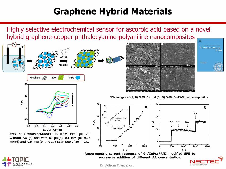
Graphene Hybrid Materials
Highly selective electrochemical sensor for ascorbic acid based on a novel hybrid graphene-copper phthalocyanine-polyaniline nanocomposites
CVs of Gr/CuPc/PANI/SPE in 0.1M PBS pH 7.0
without AA (a) and with 50 µM(b), 0.1 mM (c), 0.25
mM(d) and 0.5 mM (e) AA at a scan rate of 20 mV/s.
Amperometric current response of Gr/CuPc/PANI modified SPE to successive addition of different AA concentration.
SEM images of (A, B) Gr/CuPc and (C, D) Gr/CuPc-PANI nanocomposites

Dr. Adisorn Tuantranont
Cytotoxicity assessment of MDA-MB-231 breast cancer cells on screen-printed graphene - carbon paste substrate
Cytotoxicity Assessment of Graphene Ink

Dr. Adisorn TuantranontDr. Adisorn Tuantranont
Application: Glucose biosensors
Graphene–PEDOT:PSS on screen printed carbon electrode
for glucose biosensing
Glucose biosensing
PEDOT-PSS Graphen/PEDOT:PSS
GOD
Enzyme
Highly selective for glucose sensor
High sensitivity Low detection limit
Journal of Electroanalytical Chemistry, 2013

Dr. Adisorn TuantranontDr. Adisorn Tuantranont
1.First of its kind to the WORLD!
2.Small & Portable
3.Easy, Fast, Accurate
4.Low Cost, High Return
Aflasense

Dr. Adisorn TuantranontDr. Adisorn Tuantranont
AflaSense: Aflatoxin sensors
Aflasense - A rapid and portable aflatoxin sensor
Alfatoxin = 0 to 80 ppb
Analysis process
10-15 min 45 min 10 min < 1 min 20 sec
Graphene-carbon paste

Dr. Adisorn TuantranontDr. Adisorn Tuantranont
Graphene Composite Major developments should be made in the area of chemical derivatives of graphene
in order to control electrical conductivity and optical properties of the final products
Incorporation of well-dispersed graphene-sheets into polymers at low filler content improves the mechanical properties
Source: Nanoscale, 2015, 7, 4598

Dr. Adisorn TuantranontDr. Adisorn Tuantranont
Potential composite improvements with graphene
Mechanical properties Electrical conductivity (σ)
Thermal conductivity (κ)
Gas permeation
Surface area
Composite
property improvement
Catalysis

Dr. Adisorn Tuantranont
Graphene-polyaniline nanocomposite prepared by
electrolytic exfoliation for supercapacitor applications
Graphene Composite
Electrolytic exfoliation
of graphite in SDBS-
containing electrolyte Surfactant
stabilized
graphene
dispersion is
used for
polymerization
of PANI
Material was
characterized and
applicability for
supercapacitors was
investigated using a
home-build 2 electrode
cell
High specific
capacitance of
350 F/g at 0.25
A/g is achieved

Dr. Adisorn Tuantranont
Facile preparation of graphene–metal phthalocyanine hybrid material by electrolytic exfoliation
Graphene-metal phthalocyanine prepared by electrolytic exfoliation in TSCuPc
AFM image (a) and height profile (b) of a hybrid particle.

Dr. Adisorn Tuantranont
Electrolytically-Exfoliated Graphene-Polylactide based Bioplastic with High Elastic Performance
Graphene/PLA tensile test specimen
Physical representations of graphene/PLA

Dr. Adisorn Tuantranont
3D Printable Graphene/Polylactide composite for
Commercial 3D Printer
Strain increased̴2 time
Graphene/PLA composite masterbatch
Stress-Strain Curve
Graphene/PLA PLA

Dr. Adisorn TuantranontDr. Adisorn Tuantranont
-200
-100
0
100
200
300
400
500
600
0 0.2 0.4 0.6 0.8 1 1.2
Cur
rent
(µ
A)
E/V vs Ag/AgCl (V)
2.Toxicity/Drug testing
Cell culture on 3D-printed graphene electrode
Cellular electrochemical signal
Grapheneoxide loadanticancer drug
Graphene-hydrogel
1.Drug screening
3D-printed graphene electrode cell culture

Dr. Adisorn Tuantranont
Preliminary development of graphene by CVD
50 nm 50 nm
1000 1500 2000 2500 3000
(b)
(a)
(c)
(d)
Raman shift (cm-1)In
ten
sity
(A
rbit
rary
un
it)
SEM images of CVD graphene thin films synthesized at different CVD conditions
Raman spectra of CVD graphene thin films synthesized at different CVD conditionsTEM images of CVD graphene thin films synthesized at different CVD conditions
CVD Graphene

Dr. Adisorn Tuantranont
3D CVD Graphene
- Anneal process
150 sccm H2 flow at 900 C 1 Torr for 30 minutes
- Graphene layer deposition
C2H2/H2 gas mixture (2/16 sccm) at 900 C 0.6 Torr for 1
minutes- Fast cooling
150 sccm H2 flow at 1 Torr with fast cooling rate of
>50oC/min
900
Temp oC
Time
1
Flow chart for 3D Graphene foam synthesis
2 3
RT
1. Nickel foam template cleaning
Sonicating with acetone for 5 minutes
2. Graphene synthesis on Nickel foam template
by CVD
3. PDMS coating
Nickel foams template covered with graphene were
drop-coated with PDMS
4. Nickel Foam template etching
Etching with 3 M HCl solution at 70oC for 12 hours
3D Graphene foam and composite

Dr. Adisorn Tuantranont
3D Graphene foam and composite
3D CVD Graphene
SEM images
3D Graphene foam - PDMSNickel foam - PDMS
2D Graphene 3D Graphene foam

Dr. Adisorn Tuantranont
3D Graphene foam and composite
3D Graphene
100 nm5 nm
1-2 layers
TEM images
3D Graphene foam and composite
Graphene/PDMS foamGraphene/Ni foamNi foam

Dr. Adisorn Tuantranont
3D Hollow Graphite Nanotetrapods by Vapor Phase Transport and In-situ
Chemical Vapor Deposition/Etching
Novel 3D Graphene Nanostructure
Typical condition
1. ZnO nanotetrapod synthesis by vapor phase
transport
2.CVD graphitic layer deposition
C2H2/H2 gas mixture (3/24 sccm) at 700 C for 3
minutes
3.Vapor phase ZnO etching
Reduction in H2 flow of 500 sccm at 700 C for 30
minutes
950
Temp oC
Time
1
Flow chart for Graphite Decorated ZnO Nanotetrapods
700
2 3
RT
- ZnO/CNTs mixture powder (1/1 by mole)
- 1000 sccm Ar flow at 950 C for 40 minutes
- Air exposure at 1 atm for 1 minute

Dr. Adisorn Tuantranont
Novel 3D Graphene Nanostructure
ZnO Nanotetrapods
2 mm
2 mm
2 mm
Graphite coated ZnO
Nanotetrapods
3D Hollow Graphite
Nanotetrapods
SEM images
300 nm
300 nm

Dr. Adisorn Tuantranont
Novel 3D Graphene Nanostructure
ZnO Nanotetrapods
Graphite coated ZnO
Nanotetrapods
3D Hollow Graphite
Nanotetrapods
300 nm
TEM images
300 nm
300 nm
50 nm
15 nm

Dr. Adisorn Tuantranont
Novel 3D Graphene Nanostructure
Effect of Carbon synthesis time
2 mm 2 mm
2 mm2 mm
1 min 3 min
5 min 10 min

Dr. Adisorn Tuantranont
Graphene-composite gas sensors
Graphene-SnO2 nanocomposite prepared by electrolytic exfoliation
and flame spray pyrolysis
Electrolytic exfoliation Flame spray pyrolysis
Paste mixing and spin coating
GrapheneMetal oxide nanoparticles

Dr. Adisorn Tuantranont
Graphene-composite gas sensors
Graphene-In-doped SnO2 nanocomposite

Dr. Adisorn Tuantranont
Rapid ethanol sensor based on electrolytically-exfoliated
graphene-loaded flame-made In-doped SnO2composite film

Dr. Adisorn Tuantranont
Electrolytically Exfoliated Graphene-Loaded Flame-Made Ni-
Doped SnO2 Composite Film for Acetone Sensing
ACS Appl. Mater. Interfaces, 2015, 7 (5), pp 3077–3092

Dr. Adisorn TuantranontDr. Adisorn Tuantranont
o Supercapacitors also called ultracapacitors and electric double layer
capacitors (EDLC) are capacitors with capacitance values greater than
any other capacitor type available today.
Ultracapacitors vs. Battery and Conventional Capacitors
Benefits of Supercapacitors• High Power Density
• Very Fast Charge/Discharge Time
• Long Cycle Life (1,000x > Battery)
• High Reliability and Low Maintenance
• Wide Working Temperature
This work
Graphene-based Supercapacitors

Dr. Adisorn TuantranontDr. Adisorn Tuantranont
Electric double-layer capacitance (EDLC)
Pseudocapacitance
• Physical charge storage
• Charge transfer through surface redox reactions
Redoxreaction
Type of supercapacitors

Dr. Adisorn TuantranontDr. Adisorn Tuantranont
Advantage of graphene for supercapacitor
Graphene is based on graphite (low cost and scalable)
High electrical conductivity (R~ 1.5 x10⁻⁶ ohm-cm)
Large surface area (about 2630 m2/g)• Activated carbon 1000 m2/g
• SWCNT 1300 m2/g
• Carbon aerogel 400-1200 m2/g

Dr. Adisorn Tuantranont
Novel surfactant-stabilized graphene-polyaniline composite nanofiber for
supercapacitor applications

Dr. Adisorn TuantranontDr. Adisorn Tuantranont
Printed Graphene/PANI supercapacitor electrode
Graphene
Graphene/PANI
Capacitance : ~600 F/g
I : charge-discharge current (A)
∆t : discharge time (s)
∆v : potential charge during discharge
process (v)m : mass of active material (g)
Further work
Graphene
PANIMetal OxideMnO2, RuO2 etc.
Hybrid Supercapacitors• High specific capacitance
> 1,000 F/g
• High power density
• High energy density
Coil cell preparation

Dr. Adisorn Tuantranont
Thailand Science Park, Inc2, 5th Floor, Tower D

Dr. Adisorn TuantranontDr. Adisorn Tuantranont
TOPIC’s Infrastructure: Material Printing/Deposition
Inkjet printer : DMP-2831, Fujifilm Dimatix DEK Automated Screen Printer Semi-auto screen printer : MK mini, Minami Gravure printer : Labratester, Norbert Schläfli Maschinen Flexo printer : F1-UV, IGT Testing system Spin coater : WS-650Sz-6NPP/LITE, Laurell Chemical Vapor Deposition (CVD) : planarGROW-4E, Planar tech Mask aligner : MJB4, SUSS MicroTech Plasma system : Pico, Diener electronic …
Auto Screen Printer

Dr. Adisorn Tuantranont
Graphene-polymer dispersed solution was
used as an ink for inkjet printing
(PCT Patent licensed to Innophene )
Graphene-Polymer
Screen printed carbon
electrode
The inkjet printed graphene-
polymer on carbon electrode
Inkjet Printing
www.innophene.com
Spin-off Company: Innophene Graphene Conductive Ink for Transparent Electrode and Sensors

Dr. Adisorn Tuantranont
Haydale Graphene Industries establish
research center in Thailand
Haydale Technology Thailand (HTT)www.haydale.com
Graphene composite Graphene ink and coating

Dr. Adisorn TuantranontDr. Adisorn Tuantranont
2016 2017 2018 2019 2020
Application
Product
Technology
Logistics/IT/Digital Economy
Energy/EnvironmentFood / agricultural
Intelligent packaging (with Food Sensors)
Printed Aflatoxin Sensor Printed HbA1C Sensors
Printed Antenna (RFID)
Transparent Electrode / Conductor
Innovative Product using Transparent Electrode (Touch Screen, Small Display)
Graphene-Nano Composite InkGraphene-based Conductive Ink Multi Functional Ink
Inkjet PrintingScreen Printing Hybrid Printing
3-D PrintingGravure/Flexo Printing
Paper-based Electronic / Disposable ElectronicAdvanced material Synthesis (Thermoelectric, Solar)
Polymer composite/semi-conductive ink Graphene Field Effect Transister (GFET)
Printed Thermoelectric/Solar Cell
Printed Electroluminescense (EL)Printed TB Sensors
Printed Smart Label
Sensors/Internet of Things (IoT)
Printed Organ on chip/Cell-based Sensors
Self-Assembly MaterialSmart Object/Internet of Things (IoT)
Printed Smart Object/IoT
3-D Bio Printing
Printed Food Pathogen Sensor (Salmonella, E.Coli…) Printed Heart Attack Sensor
Printed Supercapacitor/battery
3D Printed Bio-material/Polymer

Dr. Adisorn Tuantranont
“Thank you for your attention” www.graphenethailand.com
Acknowledgement


![Synthesis, Properties and Potential Applications of Porous ...graphene. Shown in Fig. 2 is the band structure for graphene and hydrogenated porous graphene (HPG) [56]. For pure graphene](https://static.fdocuments.us/doc/165x107/5e69b1218c0b164bfe524e90/synthesis-properties-and-potential-applications-of-porous-graphene-shown-in.jpg)