List vs IEnumerable vs IQueryable vs ICollection vs IDictionary - CodeProject
IT 14 015
Examensarbete 30 hpJune 2014
GPU: Power vs Performance
Siddhartha Sankar Mondal
Institutionen för informationsteknologiDepartment of Information Technology

Teknisk- naturvetenskaplig fakultet UTH-enheten Besöksadress: Ångströmlaboratoriet Lägerhyddsvägen 1 Hus 4, Plan 0 Postadress: Box 536 751 21 Uppsala Telefon: 018 – 471 30 03 Telefax: 018 – 471 30 00 Hemsida: http://www.teknat.uu.se/student
Abstract
GPU: Power vs Performance
Siddhartha Sankar Mondal
GPUs are widely being used to meet the ever increasing demands of Highperformance computing. High-end GPUs are one of the highest consumers of powerin a computer. Power dissipation has always been a major concern area for computerarchitects. Due to power efficiency demands modern CPUs have moved towardsmulticore architectures. GPUs are already massively parallel architectures. There hasbeen some encouraging results for power efficiency in CPUs by applying DVFS . Thevision is that a similar approach would also provide encouraging results for powerefficiency in GPUs.
In this thesis we have analyzed the power and performance characteristics of GPU atdifferent frequencies. To help us achieve that, we have made a set ofmicrobenchmarks with different levels of memory boundedness and threads. We havealso used benchmarks from CUDA SDK and Parboil. We have used a GTX580 Fermibased GPU. We have also made a hardware infrastructure that accurately measuresthe power being consumed by the GPU.
Tryckt av: Reprocentralen ITC
Sponsor: UPMARCIT 14 015Examinator: Ivan ChristoffÄmnesgranskare: Stefanos KaxirasHandledare: Stefanos Kaxiras


Acknowled gement
I would like to thank my supervisor Prof. Stefanos Kaxiras for giving me the wonderfulopportunity to work on this interesting topic. I would also like to thank his PhDstudents Vasileios Spiliopoulos and Konstantinos Koukos for helping me get startedwith the benchmarks and hardware setup. �e LATEX community has been of great helpwhile making this document. Also, I would like to thank the spirit that lives in thecomputer. �is thesis was funded by UPMARC.
v


Contents
Acknowled gement v
Contents vii
1 Introduction 1
2 Background 32.1 CUDA Programming model 32.2 GPU Architecture 42.3 Power issues 52.4 Latency 62.5 Previous work 7
3 Method olo gy 93.1 Experimental Setup 93.2 Power measurement 93.3 DVFS 113.4 Microbenchmarks 113.5 Benchmarks 12
3.5.1 Matrix Multiplication 133.5.2 Matrix Transpose 133.5.3 Histogram 133.5.4 Radix Sort 133.5.5 Merge Sort 133.5.6 Conjugate Gradient 133.5.7 BFS(Breadth First Search) 133.5.8 Eigenvalues 133.5.9 Black-Scholes option pricing 133.5.10 3D FDTD(3D Finite Di�erence Time Domain method) 143.5.11 Scalar Product 14
4 Evaluation 15
vii

viii contents
4.1 Microbenchmarks 164.1.1 Microbenchmark 1 164.1.2 Microbenchmark 2 174.1.3 Microbenchmark 3 184.1.4 Microbenchmark 4 19
4.2 Benchmarks 204.3 Memory Bandwidth 24
4.3.1 Black-Scholes 244.3.2 Eigenvalue 254.3.3 3D FDTD 264.3.4 Scalar Product 27
5 Conclusion 29
B iblio graphy 31
Assembly code 33
Power measurements 37

chapter 1
Introduction
Over the last few years the CPU and GPU architectures have been evolving very rapidly.With the introduction of programmable shaders in GPU since the turn of century, ithas been used by the scienti�c computing community as a powerful computationalaccelerator to the CPU. For many compute intensive workloads GPUs gives few ordersof magnitude better performance than a CPU. �e introduction of languages likeCUDA and OpenCL has made it more easier to program on a GPU.
In our evaluation we have used the Nvidia GTX580 GPU. It is based on the Fermiarchitecture[15]. With 512 compute units called CUDA cores it can handle 24,576active threads [9, 15]. Its o�-chip memory bandwidth is around 192 GB/s, which isconsiderably higher than CPUs main memory bandwidth(around 32 GB/s for core i7).�eoretically it can do over 1.5 TFLOPS(with single precision FMA). Even with suchgreat numbers to boast about, GPUs have a few bottlenecks that one has to considerbefore sending all workload down to the GPU. One of them is the power and the otheris the cost to transfer data from host to device(i.e. CPU to GPU) and again back fromdevice to host(i.e. GPU to CPU). �e bandwidth of 16x PCI express is around 8GB/s.
Power is a very important constraint for every computer architecture[7]. Modernhigh-end GPUs have thermal design power(TDP) of over 200 watts. �e GTX580 hasa TDP of 244 watts. Whereas a high-end multicore CPU like Intel core i7 has a TDPof around 100 watts. In terms of GFLOPS/watt GPUs can be considered to be morepower e�cient than CPUs. But for GPUs to be considered as co-processor it consumesway too much power out of the total power budget.
�ough GPUs have such high o�-chip memory bandwidth, accessing the o�-chipglobal memory is very expensive(latency of around 400 to 800 clock cycles). GPUshide this latency by scheduling very large number of threads at a time. For memorybound application it becomes hard to hide this latency and they have slack. On CPUswe can take advantage of this by applying DVFS to reduce the dynamic power.
1

2 chapter 1 . introduction
In this thesis work we investigate the power and performance characteristics ofa GPU with DVFS(Dynamic voltage and frequency scaling). To help us achieve thatwe make use of microbenchmarks with di�erent levels of memory boundedness andthreads. We follow it up by applying DVFS to some more benchmarks.
Apart from the introduction in this chapter the thesis is structured as follows. InChapter 2 , we discuss about GPU programming, GPU architecture, the concept behindDVFS based power savings and also some previous work. In Chapter 3, we describethe method used to measure power and implement DVFS on GPU. We also throwsome light on the benchmarks that were used for the evaluation. In Chapter 4, weevaluate the performance and power consumption of the benchmarks under di�erentnumber of threads, shader frequencies and memory bandwidth. In Chapter 5, were�ect on the conclusions drawn from our evaluation. In Appendix: Assembly code,we provide the assembly code of the micro benchmarks we used. In Appendix: Powermeasurements, we provide all the execution times and power consumption readingsfrom the evaluation.

chapter 2
Background
2.1 cuda pro gramming model
CUDA is a GPGPU programming language that can be used to write programs forNVIDIA GPUs. It is an extension of the C programming language. A code written inCUDA consists of a mix of host(CPU) code and device(GPU) code[9]. �e NVCCcompiler compiles the device code and separates it from the host code. At a later stage aC compiler can be used to compile the host code and the device code parts are replacedby calls to the compiled device code.
A data parallel function that is to be run on a device is called a kernel. A kernelcreates many threads to compute this data parallel workload. A thread block consistsof many threads and a group of thread block form a grid.
1 __global__ void SimpleKernel(float A[N],float B[N],float C[N], int N)
2 {
3 //calculate thread id
4 int i= blockIDx.x * blockDim.x + threadIdx.x;
5 if(i<N)
6 C[i] = A[i] + B[i];
7 }
89 int main()
10 {
11 ......
12 //kernel invocation
13 SimpleKernel<<<numberOfBlocks,threadsPerBlock >>>(A,B,C,N);
14 ......
15 }
Listing 2.1: A simple CUDA kernel
3

4 chapter 2. background
In the Listing 2.1 on page 3 we have shown a very simple CUDA program model.Inside the kernel SimpleKernel we have CUDA speci�c variables that help us identifythe data element for the particular thread. threadIdx identi�es a thread inside a block.Each thread inside a block has a unique thread id. blockIdx identi�es the block ina grid. �e blockDim gives the size of a block in a particular dimension. When weinvoke the kernel from the device code, along with the kernel arguments we also passthe thread details. �e variable threadsPerBlock gives the number of threads ina block and numberOfBlocks indicate the number of blocks that are to be passed.All the blocks are of the same size(i.e. they have the same number of threads). BothnumberOfBlocks and threadsPerBlock can be 1D or 2D or 3D data types. A moredetailed explanation about CUDA programming can be found in [9].
2.2 gpu architecture
SM SM SM SM SM SM SM SM
SM SM SM SM SM SM SM SM
Fermi GPU
Figure 2.1: On the le� we have the CUDA core. SM is shown in the centre. It is made up of CUDA cores.�e Fermi GPU architecture shown on the right has many SMs. Source: NVIDIA Fermiarchitecture whitepaper
In our setup we use the Nvidia GTX580 GPU with CUDA compute capability 2.0.It is based on the Fermi architecture[15]. Figure 2.1 gives an overview of the Fermiarchitecture. �e basic computing unit is the CUDA core. �ere are 512 CUDA coreson the Fermi. Each CUDA core can execute integer or �oating point instructions for asingle thread. 32 CUDA cores make up a single Streaming Multiprocessor(SM). �erein total 16 SMs on the GTX580. Each SM has its own con�gurable shared memory andL1 cache, which can be con�gured as 16/48 KB. It also has an L2 cache of size 768 KB.In the Fermi all the global memory calls pass through the L2 cache[9]. It has six 64 bitmemory interface. With a 2004 MHz GDDR5 it gives us a peak memory bandwidth of192 GB/s.
2.3 . p ower issues 5
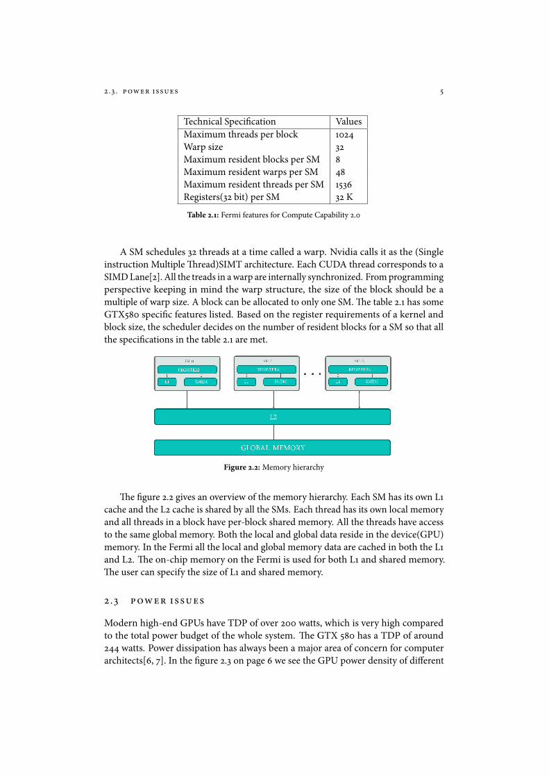
Technical Speci�cation ValuesMaximum threads per block 1024Warp size 32Maximum resident blocks per SM 8Maximum resident warps per SM 48Maximum resident threads per SM 1536Registers(32 bit) per SM 32 K
Table 2.1: Fermi features for Compute Capability 2.0
A SM schedules 32 threads at a time called a warp. Nvidia calls it as the (Singleinstruction Multiple �read)SIMT architecture. Each CUDA thread corresponds to aSIMD Lane[2]. All the treads in a warp are internally synchronized. From programmingperspective keeping in mind the warp structure, the size of the block should be amultiple of warp size. A block can be allocated to only one SM. �e table 2.1 has someGTX580 speci�c features listed. Based on the register requirements of a kernel andblock size, the scheduler decides on the number of resident blocks for a SM so that allthe speci�cations in the table 2.1 are met.
REGISTERS
SMEML1
SM-0
Figure 2.2: Memory hierarchy
�e �gure 2.2 gives an overview of the memory hierarchy. Each SM has its own L1cache and the L2 cache is shared by all the SMs. Each thread has its own local memoryand all threads in a block have per-block shared memory. All the threads have accessto the same global memory. Both the local and global data reside in the device(GPU)memory. In the Fermi all the local and global memory data are cached in both the L1and L2. �e on-chip memory on the Fermi is used for both L1 and shared memory.�e user can specify the size of L1 and shared memory.
2.3 p ower issues
Modern high-end GPUs have TDP of over 200 watts, which is very high comparedto the total power budget of the whole system. �e GTX 580 has a TDP of around244 watts. Power dissipation has always been a major area of concern for computerarchitects[6, 7]. In the �gure 2.3 on page 6 we see the GPU power density of di�erent

6 chapter 2. background
Figure 2.3: GPU power trends. Source: Nvidia [1]
technology nodes. Nvidia set a maximum power density of 0.3W/mm2 for the worstcase process, voltage and temperature[1]. �e AC power density represents the dynamicpower and the DC power density represents the static power. �e GTX 580 is madeusing the 40nm technology. In this case both static and dynamic power density isalmost similar. When we go to the newer 28nm technology the dynamic power densityexceeds the static power by a huge margin. So dynamic power is a major area ofconcern.
Dynamic power is given by the equation[6],P = CV 2Afwhere,
C = CapacitanceV = Supply voltageA = Activity factorf = Clock frequency
Together V 2 f makes a cubic impact on the power dissipation. Also V and f arelinearly related. Memory bound applications su�er from long latency stalls and do notbene�t from high clock frequency. So, for memory bound applications we can makeuse of dynamic voltage frequency scaling(DVFS) to reduce power dissipation.
2.4 l atency
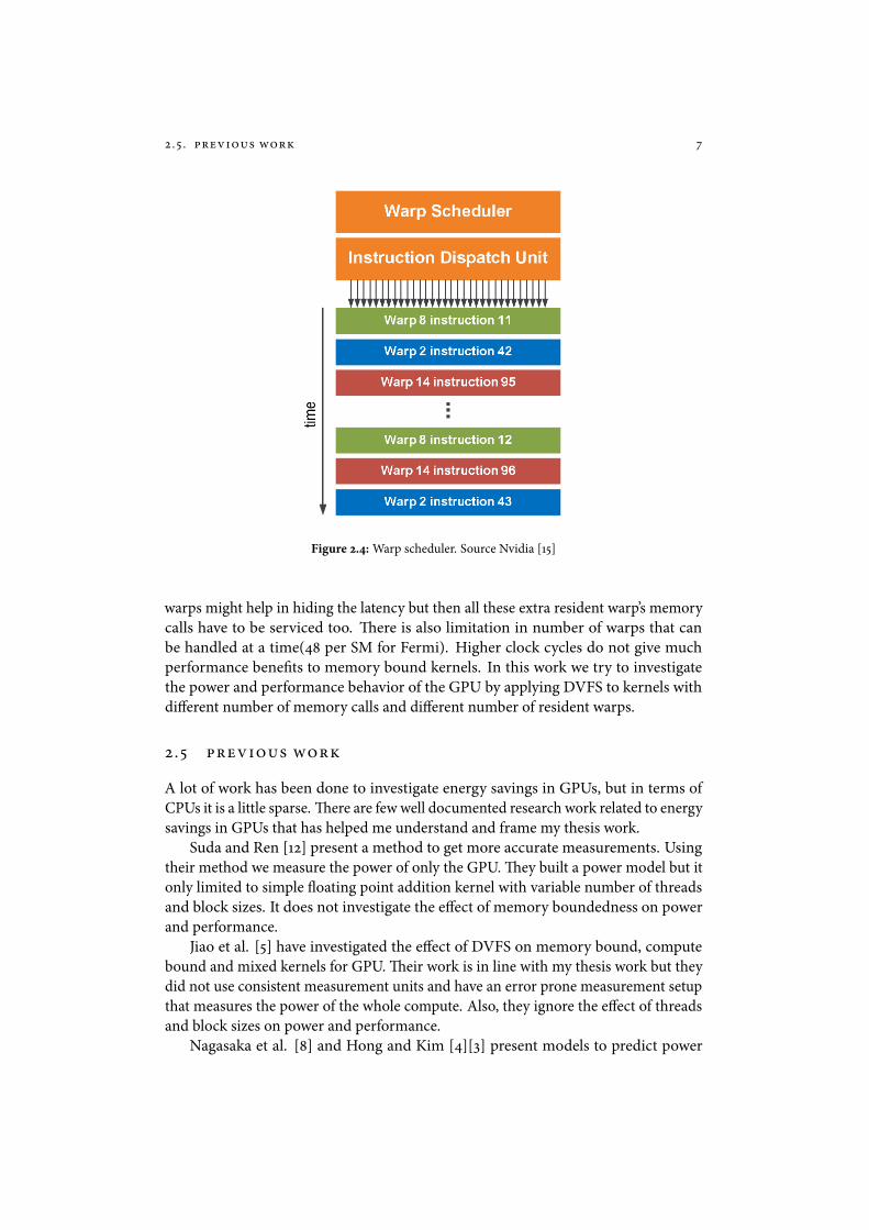
Even though GPUs have such high memory bandwidth, the major bottleneck is thelatency due to o�-chip memory access. Fetching operands from from o�-chip memorycosts around 600 clock cycles. GPUs have a large number of resident threads in theform of warps to hide this latency. �e �gure 2.4 on page 7 shows how the warpscheduler swaps between di�erent resident warps. �e number of warps needed tohide this latency depends on the ratio of memory call instructions to other instructions.For our device if we have a kernel with 1 memory call out of 15 instructions then weneed about 40 resident warps in that SM to hide the latency[9]. Having more number of
2.5 . previous work 7
Figure 2.4: Warp scheduler. Source Nvidia [15]
warps might help in hiding the latency but then all these extra resident warp’s memorycalls have to be serviced too. �ere is also limitation in number of warps that canbe handled at a time(48 per SM for Fermi). Higher clock cycles do not give muchperformance bene�ts to memory bound kernels. In this work we try to investigatethe power and performance behavior of the GPU by applying DVFS to kernels withdi�erent number of memory calls and di�erent number of resident warps.
2.5 previous work
A lot of work has been done to investigate energy savings in GPUs, but in terms ofCPUs it is a little sparse. �ere are few well documented research work related to energysavings in GPUs that has helped me understand and frame my thesis work.
Suda and Ren [12] present a method to get more accurate measurements. Usingtheir method we measure the power of only the GPU. �ey built a power model but itonly limited to simple �oating point addition kernel with variable number of threadsand block sizes. It does not investigate the e�ect of memory boundedness on powerand performance.
Jiao et al. [5] have investigated the e�ect of DVFS on memory bound, computebound and mixed kernels for GPU. �eir work is in line with my thesis work but theydid not use consistent measurement units and have an error prone measurement setupthat measures the power of the whole compute. Also, they ignore the e�ect of threadsand block sizes on power and performance.
Nagasaka et al. [8] and Hong and Kim [4][3] present models to predict power

8 chapter 2. background
and performance in GPU. Nagasaka et al. proposed a statistical model and Hong andKim proposed an analytical model. Both the research work has excellent amount ofinformation for extending my thesis data to derive a Power and Performance modelfor DVFS in GPUs.
chapter 3
Method olo gy
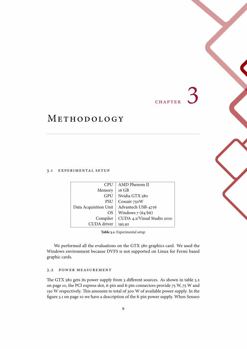
3 . 1 experimental setup
CPU AMD Phenom IIMemory 16 GB
GPU Nvidia GTX 580PSU Cossair 750W
Data Acquisition Unit Advantech USB-4716OS Windows 7 (64 bit)
Compiler CUDA 4.2/Visual Studio 2010CUDA driver 195.92
Table 3.1: Experimental setup
We performed all the evaluations on the GTX 580 graphics card. We used theWindows environment because DVFS is not supported on Linux for Fermi basedgraphic cards.
3 .2 p ower measurement
�e GTX 580 gets its power supply from 3 di�erent sources. As shown in table 3.2on page 10, the PCI express slot, 6-pin and 8-pin connectors provide 75 W, 75 W and150 W respectively. �is amounts to total of 300 W of available power supply. In the�gure 3.1 on page 10 we have a description of the 8-pin power supply. When Sense0
9

10 chapter 3 . method olo gy
Power Source Maximum PowerPCI Express slot 75 WPCI Express 6-pin connector 75 WPCI Express 8-pin connector 150 W
Table 3.2: Distribution of GPU power supply
Figure 3.1: 8pin PCI Express auxiliary power supply
and Sense1 is detected it acts like the 8 pin power supply and provides 150 W. WhenSense1 is not detected it behaves like the 6-pin power supply and provides 75 W[10].
Figure 3.2: GPU power measurement
In the �gure 3.2 we have described the power measurement infrastructure we havein place. It helps us accurately measure the power going on to the GPU and also fromeach power source of the GPU. We �x probes to the power supply wires that go to theGPU to measure the power. We have used a PCI-Express riser card to measure the

3 .3 . dvfs 11
power being supplied through the PCI-Express. �e Data Acquisition Unit measuresthe current passing through all the power supplies. We assume that the voltage throughthe 12V and 3.3V are constant. It gives rise to a total power measurement error of 3watts[12].
3 .3 dvfs
Sr. Shader Frequency (MHz) Core Voltage (V)1 810 0.9632 1000 0.9753 1200 0.9884 1400 1.0005 1600 1.013
Table 3.3: DVFS settings used
We have used a shader frequency range of 810-1600 MHz with a stepping size of200 MHz. �e safe voltage scaling option provided by the GPU is 0.963V to 1.013V.As shown in table 3.3 we assigned a voltage value to the shader frequency to make theDVFS settings.
3 .4 microbenchmarks
We have made 4 microbenchmarks to help us understand the power vs performancebehavior. All the microbenchmarks are simple vector addition with di�erent level ofglobal memory calls. All of them are made with the help CUDA Occupancy calculatorto ensure the intended behavior[13] In the Appendix A on page 33 we have providedthe assembly code for each of the microbenchmarks.
�e microbenchmark1 kernel code is given in listing 3.1. It has a single threadregister requirement of 10 registers. 2 out of 18 instructions are memory calls.
1 __global__ void micro1(const Mytype* A, const Mytype* B, Mytype* C, int N)
2 {
3 int x = blockDim.x * blockIdx.x + threadIdx.x;
4 int y = blockDim.x * gridDim.x * blockIdx.y;
5 int i = x + y;
6 if (i < N)
7 C[i] = A[i] + B[i];
8 }
Listing 3.1: Microbenchmark 1
�e microbenchmark2 kernel code is given in listing 3.2. It has a single threadregister requirement of 13 registers. 4 out of 26 instructions are memory calls.
�e microbenchmark3 kernel code is given in listing 3.3. It has a single threadregister requirement of 15 registers. 6 out of 34 instructions are memory calls.
12 chapter 3 . method olo gy
1 __global__ void micro2(const Mytype* A, const Mytype* B, const Mytype* D, const Mytype*E,Mytype* C, int N)
2 {
3 int x = blockDim.x * blockIdx.x + threadIdx.x;
4 int y = blockDim.x * gridDim.x * blockIdx.y;
5 int i = x + y;
6 if (i < N)
7 C[i] = A[i] + B[i] + D[i] +E[i];
8 }
Listing 3.2: Microbenchmark 2
1 __global__ void micro3(const Mytype* A, const Mytype* B, const Mytype* D, const Mytype*E,const Mytype* F,const Mytype* G ,Mytype* C, int N)
2 {
3 int x = blockDim.x * blockIdx.x + threadIdx.x;
4 int y = blockDim.x * gridDim.x * blockIdx.y;
5 int i = x + y;
6 if (i < N)
7 C[i] = A[i] + B[i] + D[i] +E[i] + F[i] + G[i];
8 }
Listing 3.3: Microbenchmark 3
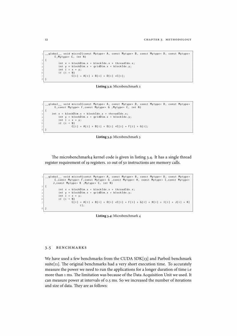
�e microbenchmark4 kernel code is given in listing 3.4. It has a single threadregister requirement of 19 registers. 10 out of 50 instructions are memory calls.
1 __global__ void micro4(const Mytype* A, const Mytype* B, const Mytype* D, const Mytype*E,const Mytype* F,const Mytype* G ,const Mytype* H, const Mytype* I,const Mytype*
J,const Mytype* K ,Mytype* C, int N)
2 {
3 int x = blockDim.x * blockIdx.x + threadIdx.x;
4 int y = blockDim.x * gridDim.x * blockIdx.y;
5 int i = x + y;
6 if (i < N)
7 C[i] = A[i] + B[i] + D[i] +E[i] + F[i] + G[i] + H[i] + I[i] + J[i] + K[
i];
8 }
Listing 3.4: Microbenchmark 4
3 .5 benchmarks
We have used a few benchmarks from the CUDA SDK[13] and Parboil benchmarksuite[11]. �e original benchmarks had a very short execution time. To accuratelymeasure the power we need to run the applications for a longer duration of time i.emore than 1 ms. �e limitation was because of the Data Acquisition Unit we used. Itcan measure power at intervals of 0.5 ms. So we increased the number of iterationsand size of data. �ey are as follows:

3 .5 . benchmarks 13
3.5.1 Matrix Multiplication
�e size of the Matrix was increased to 2560× 2560 . �e number of iterations wasincreased to 20.
3.5.2 Matrix Transpose
�e optimized version of Matrix Transpose was used i.e. Coalesced transpose with nobank con�icts. �e Matrix size was increased from 1024× 1024 to 2048× 2048 . �enumber of repetitions was increased from 100 to 4000.
3.5.3 Histogram
�e 256-bin histogram was used. �e number of runs was increased from 16 to 1000.
3.5.4 Radix Sort
�e default version uses 32-bit unsigned int keys and values. We used 32-bit �oat keysand values. �e number of elements to sort was increased from 1,048,576 to 40,960,000.We used 10 iterations.
3.5.5 Merge Sort
�e default version uses 65,536 values. We increased it to 1,048,576 values and changedthe iterations from 1 to 100.
3.5.6 Conjugate Gradient
�e size of the matrix was increased from 1024× 1024 to 4096× 4096.
3.5.7 BFS(Breadth First Search)
BFS was used from the Parboil benchmark and was used without any increase in defaultdata size because the input was received from a �le (unlike the CUDA SDK benchmarksthat generated its own input on the CPU).
3.5.8 Eigenvalues
�e default values were used for the Eigenvalues. �e matrix used was of size 2048×2048and the benchmark performed 100 iterations.
3.5.9 Black-Scholes option pricing
�e default value of 4,000,000 options were used. But we increased the the number ofiteration from 512 to 8192.

14 chapter 3 . method olo gy
3.5.10 3D FDTD(3D Finite Di�erence Time Domain method)
�e default version applies FDTD on a 376× 376× 376 volume with symmetric �lterradius of 4 for 10 timesteps. We increased the timesteps to 64.
3.5.11 Scalar Product
�e scalar product is performed on 256 vector pairs. �e default version has 4,096elements per vector and we increased that to 16,384 elements per vector. Also we madeit iterate a 1,000 times.

chapter 4
Evaluation
�e parameters that were considered during the evaluation are execution time, power,energy and EDP. �e measurements have been provided in the Appendix B: Powermeasurements on page 37. Apart from that we evaluated the e�ect of DVFS on thememory bandwidth. From �gure 4.1 we do notice that the memory bandwidth is lessthan theoretical peak of 192.4 GB/s but it stays consistent for the particular shaderfrequency through di�erent sizes of data.
Figure 4.1: E�ect of DVFS on memory bandwidth
15

16 chapter 4. evaluation
4.1 microbenchmarks
As described in the section 3.4 on page 11 , the memory calls to compute ratio increasesfrom the Microbenchmark 1 to Microbenchmark 4. Each of the Microbenchmarkshave been evaluated for di�erent number of warps per SM i.e. 16, 32 and 48 warps. �escheduler switches between multiple warps in a SM to hide the latency for memorycalls. But, while looking through the plots for each of the microbenchmarks it can beseen that beyond a certain point even increasing the number of warps does not giveus increase in performance. As the memory boundedness increases there is very littledi�erence between the execution time for 32 warp and 48 warp versions. Another thingworth noticing is that 16 warp version consumes considerably lesser power than the 32warp and 48 warp version.
4.1.1 Microbenchmark 1
11.11 of the instructions for this microbenchmark are memory calls. �e 48 warpversion has the best execution times. Beyond 1200 MHz both 32 warp and 48 warpversions execution times starts to �atten. We get the best EDP for the 48 warp versionat 1000 MHz.
0.8
1
1.2
1.4
1.6
1.8
2
800 1000 1200 1400 1600
Exec
utio
n tim
e(s)
Frequency(MHz)
16 warps32 warps48 warps
Figure 4.2: Micro1: Execution time
130
140
150
160
170
180
190
200
210
220
800 1000 1200 1400 1600
Pow
er(W
atts
)
Frequency(MHz)
16 warps32 warps48 warps
Figure 4.3: Micro1: Power
140
160
180
200
220
240
260
280
800 1000 1200 1400 1600
Ener
gy(J
)
Frequency(MHz)
16 warps32 warps48 warps
Figure 4.4: Micro1: Energy
100
150
200
250
300
350
400
450
500
800 1000 1200 1400 1600
EDP(
Js)
Frequency(MHz)
16 warps32 warps48 warps
Figure 4.5: Micro1: EDP
4.1 . microbenchmarks 17
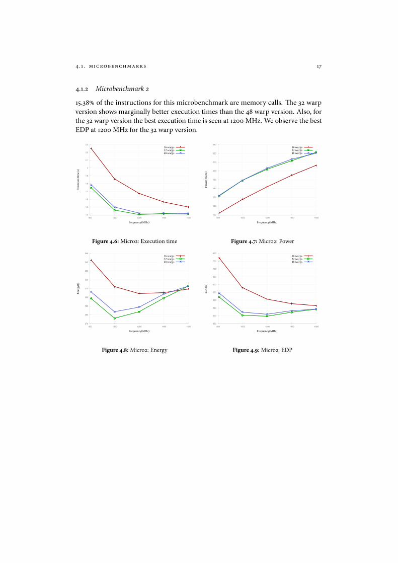
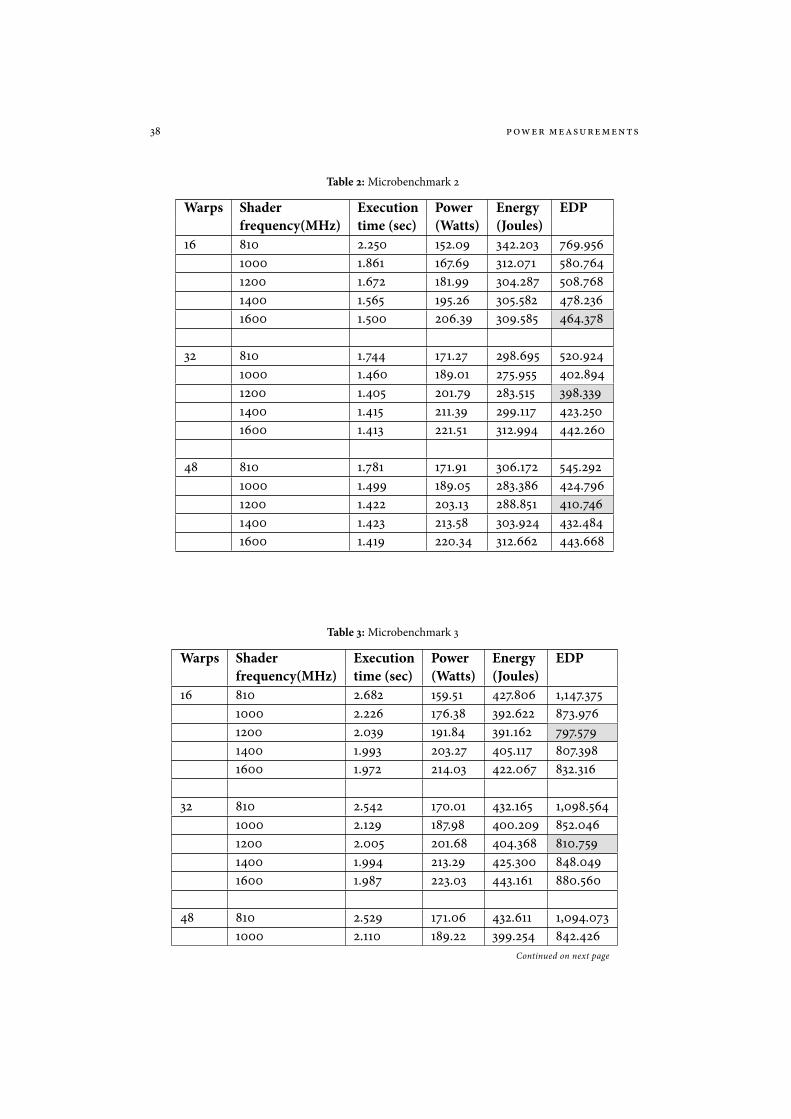
4.1.2 Microbenchmark 2
15.38 of the instructions for this microbenchmark are memory calls. �e 32 warpversion shows marginally better execution times than the 48 warp version. Also, forthe 32 warp version the best execution time is seen at 1200 MHz. We observe the bestEDP at 1200 MHz for the 32 warp version.
1.4
1.5
1.6
1.7
1.8
1.9
2
2.1
2.2
2.3
800 1000 1200 1400 1600
Exec
utio
n tim
e(s)
Frequency(MHz)
16 warps32 warps48 warps
Figure 4.6: Micro2: Execution time
150
160
170
180
190
200
210
220
230
800 1000 1200 1400 1600
Pow
er(W
atts
)
Frequency(MHz)
16 warps32 warps48 warps
Figure 4.7: Micro2: Power
270
280
290
300
310
320
330
340
350
800 1000 1200 1400 1600
Ener
gy(J
)
Frequency(MHz)
16 warps32 warps48 warps
Figure 4.8: Micro2: Energy
350
400
450
500
550
600
650
700
750
800
800 1000 1200 1400 1600
EDP(
Js)
Frequency(MHz)
16 warps32 warps48 warps
Figure 4.9: Micro2: EDP

18 chapter 4. evaluation
4.1.3 Microbenchmark 3
17.65 of the instructions for this microbenchmark are memory calls. �e 32 warpand 48 warp version show similar execution times. �e 16 warp version starts showingbetter execution times than the other two version beyond 1400 MHz. At 1200MHz the16 warp version has the best EDP.
1.9
2
2.1
2.2
2.3
2.4
2.5
2.6
2.7
800 1000 1200 1400 1600
Exec
utio
n tim
e(s)
Frequency(MHz)
16 warps32 warps48 warps
Figure 4.10: Micro3: Execution time
150
160
170
180
190
200
210
220
230
800 1000 1200 1400 1600
Pow
er(W
atts
)
Frequency(MHz)
16 warps32 warps48 warps
Figure 4.11: Micro3: Power
390
400
410
420
430
440
450
800 1000 1200 1400 1600
Ener
gy(J
)
Frequency(MHz)
16 warps32 warps48 warps
Figure 4.12: Micro3: Energy
750
800
850
900
950
1000
1050
1100
1150
800 1000 1200 1400 1600
EDP(
Js)
Frequency(MHz)
16 warps32 warps48 warps
Figure 4.13: Micro3: EDP
4.1 . microbenchmarks 19
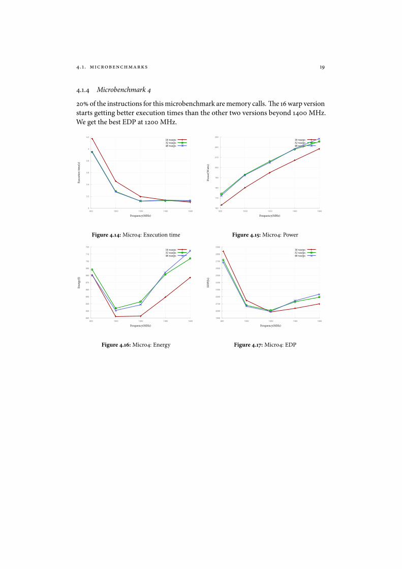
4.1.4 Microbenchmark 4
20 of the instructions for this microbenchmark are memory calls. �e 16 warp versionstarts getting better execution times than the other two versions beyond 1400 MHz.We get the best EDP at 1200 MHz.
3
3.2
3.4
3.6
3.8
4
4.2
800 1000 1200 1400 1600
Exec
utio
n tim
e(s)
Frequency(MHz)
16 warps32 warps48 warps
Figure 4.14: Micro4: Execution time
160
170
180
190
200
210
220
230
800 1000 1200 1400 1600
Pow
er(W
atts
)
Frequency(MHz)
16 warps32 warps48 warps
Figure 4.15: Micro4: Power
620
630
640
650
660
670
680
690
700
710
720
800 1000 1200 1400 1600
Ener
gy(J
)
Frequency(MHz)
16 warps32 warps48 warps
Figure 4.16: Micro4: Energy
1900
2000
2100
2200
2300
2400
2500
2600
2700
2800
2900
800 1000 1200 1400 1600
EDP(
Js)
Frequency(MHz)
16 warps32 warps48 warps
Figure 4.17: Micro4: EDP

20 chapter 4. evaluation
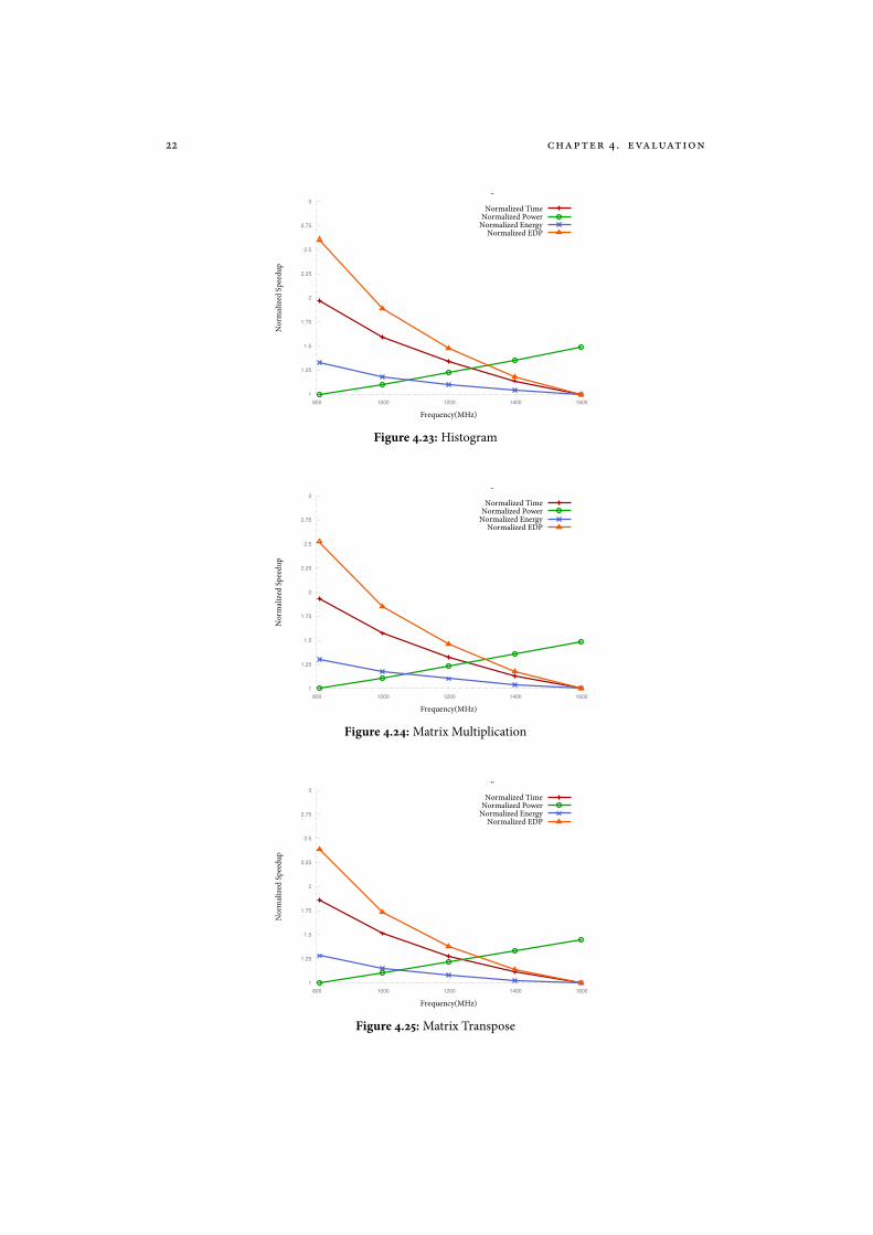
4.2 benchmarks
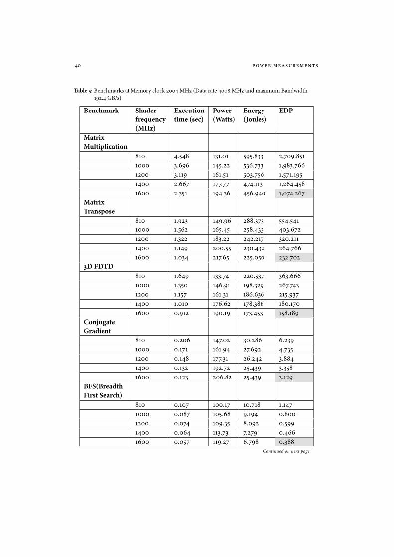
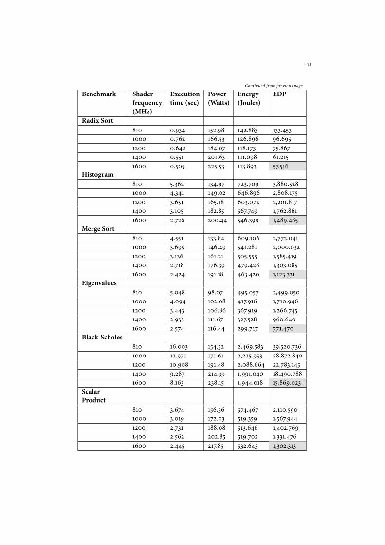
All the benchmarks in this section have been executed at normal memory clock of 2004MHz i.e. bandwidth of 192.4 GB/s. Also, note that all the plotted data are normalizedvalues. Please refer to table 5 on page 40 for the measurements. In terms of applyingDVFS, the results are a little disappointing. �e best EDP for all the benchmarks weevaluated were at the highest shader frequency.
1
1.25
1.5
1.75
2
2.25
2.5
2.75
3
800 1000 1200 1400 1600
Nor
mal
ized
Spe
edup
Frequency(MHz)
Normalized Power Profiling
Normalized TimeNormalized Power
Normalized EnergyNormalized EDP
Figure 4.18: BFS
1
1.25
1.5
1.75
2
2.25
2.5
2.75
3
800 1000 1200 1400 1600
Nor
mal
ized
Spe
edup
Frequency(MHz)
Normalized Power Profiling
Normalized TimeNormalized Power
Normalized EnergyNormalized EDP
Figure 4.19: Black-Scholes

4.2 . benchmarks 21
1
1.25
1.5
1.75
2
2.25
2.5
2.75
3
800 1000 1200 1400 1600
Nor
mal
ized
Spe
edup
Frequency(MHz)
Normalized Power Profiling
Normalized TimeNormalized Power
Normalized EnergyNormalized EDP
Figure 4.20: Conjugate Gradient
1
1.25
1.5
1.75
2
2.25
2.5
2.75
3
3.25
800 1000 1200 1400 1600
Nor
mal
ized
Spe
edup
Frequency(MHz)
Normalized Power Profiling
Normalized TimeNormalized Power
Normalized EnergyNormalized EDP
Figure 4.21: Eigenvalues
1
1.25
1.5
1.75
2
2.25
2.5
2.75
3
800 1000 1200 1400 1600
Nor
mal
ized
Spe
edup
Frequency(MHz)
Normalized Power Profiling
Normalized TimeNormalized Power
Normalized EnergyNormalized EDP
Figure 4.22: 3D FDTD
22 chapter 4. evaluation
1
1.25
1.5
1.75
2
2.25
2.5
2.75
3
800 1000 1200 1400 1600
Nor
mal
ized
Spe
edup
Frequency(MHz)
Normalized Power Profiling
Normalized TimeNormalized Power
Normalized EnergyNormalized EDP
Figure 4.23: Histogram
1
1.25
1.5
1.75
2
2.25
2.5
2.75
3
800 1000 1200 1400 1600
Nor
mal
ized
Spe
edup
Frequency(MHz)
Normalized Power Profiling
Normalized TimeNormalized Power
Normalized EnergyNormalized EDP
Figure 4.24: Matrix Multiplication
1
1.25
1.5
1.75
2
2.25
2.5
2.75
3
800 1000 1200 1400 1600
Nor
mal
ized
Spe
edup
Frequency(MHz)
Normalized Power Profiling
Normalized TimeNormalized Power
Normalized EnergyNormalized EDP
Figure 4.25: Matrix Transpose

4.2 . benchmarks 23
1
1.25
1.5
1.75
2
2.25
2.5
2.75
3
800 1000 1200 1400 1600
Nor
mal
ized
Spe
edup
Frequency(MHz)
Normalized Power Profiling
Normalized TimeNormalized Power
Normalized EnergyNormalized EDP
Figure 4.26: Merge sort
1
1.25
1.5
1.75
2
2.25
2.5
2.75
3
800 1000 1200 1400 1600
Nor
mal
ized
Spe
edup
Frequency(MHz)
Normalized Power Profiling
Normalized TimeNormalized Power
Normalized EnergyNormalized EDP
Figure 4.27: Radix Sort
1
1.2
1.4
1.6
1.8
2
800 1000 1200 1400 1600
Nor
mal
ized
Spe
edup
Frequency(MHz)
Normalized Power Profiling
Normalized TimeNormalized Power
Normalized EnergyNormalized EDP
Figure 4.28: Scalar Product
24 chapter 4. evaluation
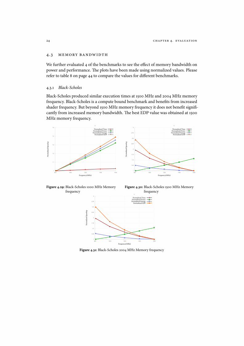
4.3 memory bandwidth
We further evaluated 4 of the benchmarks to see the e�ect of memory bandwidth onpower and performance. �e plots have been made using normalized values. Pleaserefer to table 8 on page 44 to compare the values for di�erent benchmarks.
4.3.1 Black-Scholes
Black-Scholes produced similar execution times at 1500 MHz and 2004 MHz memoryfrequency. Black-Scholes is a compute bound benchmark and bene�ts from increasedshader frequency. But beyond 1500 MHz memory frequency it does not bene�t signi�-cantly from increased memory bandwidth. �e best EDP value was obtained at 1500MHz memory frequency.
1
1.1
1.2
1.3
1.4
1.5
800 1000 1200 1400 1600
Nor
mal
ized
Spe
edup
Frequency(MHz)
Normalized Power Profiling
Normalized TimeNormalized Power
Normalized EnergyNormalized EDP
Figure 4.29: Black-Scholes 1000 MHz Memoryfrequency
1
1.25
1.5
1.75
2
2.25
2.5
2.75
3
800 1000 1200 1400 1600
Nor
mal
ized
Spe
edup
Frequency(MHz)
Normalized Power Profiling
Normalized TimeNormalized Power
Normalized EnergyNormalized EDP
Figure 4.30: Black-Scholes 1500 MHz Memoryfrequency
1
1.25
1.5
1.75
2
2.25
2.5
2.75
3
800 1000 1200 1400 1600
Nor
mal
ized
Spe
edup
Frequency(MHz)
Normalized Power Profiling
Normalized TimeNormalized Power
Normalized EnergyNormalized EDP
Figure 4.31: Black-Scholes 2004 MHz Memory frequency

4.3 . memory bandwidth 25
4.3.2 Eigenvalue
�e result for the Eigenvalue benchmark is interesting. It has similar execution timesat 1000 MHz, 1500 MHz and 2004 MHz memory frequency. �e best EDP value wasobtained at 1000 MHz memory frequency. Eigenvalue is a compute bound benchmarkand bene�ts a lot by increasing shader frequency but memory bandwidth has very littlee�ect on it. So, at lower memory bandwidth it shows signi�cant reduction in EDP.
1
1.25
1.5
1.75
2
2.25
2.5
2.75
3
3.25
800 1000 1200 1400 1600
Nor
mal
ized
Spe
edup
Frequency(MHz)
Normalized Power Profiling
Normalized TimeNormalized Power
Normalized EnergyNormalized EDP
Figure 4.32: Eigenvalues 1000 MHz Memoryfrequency
1
1.25
1.5
1.75
2
2.25
2.5
2.75
3
3.25
3.5
800 1000 1200 1400 1600
Nor
mal
ized
Spe
edup
Frequency(MHz)
Normalized Power Profiling
Normalized TimeNormalized Power
Normalized EnergyNormalized EDP
Figure 4.33: Eigenvalues 1500 MHz Memoryfrequency
1
1.25
1.5
1.75
2
2.25
2.5
2.75
3
3.25
800 1000 1200 1400 1600
Nor
mal
ized
Spe
edup
Frequency(MHz)
Normalized Power Profiling
Normalized TimeNormalized Power
Normalized EnergyNormalized EDP
Figure 4.34: Eigenvalues 2004 MHz Memory frequency
26 chapter 4. evaluation
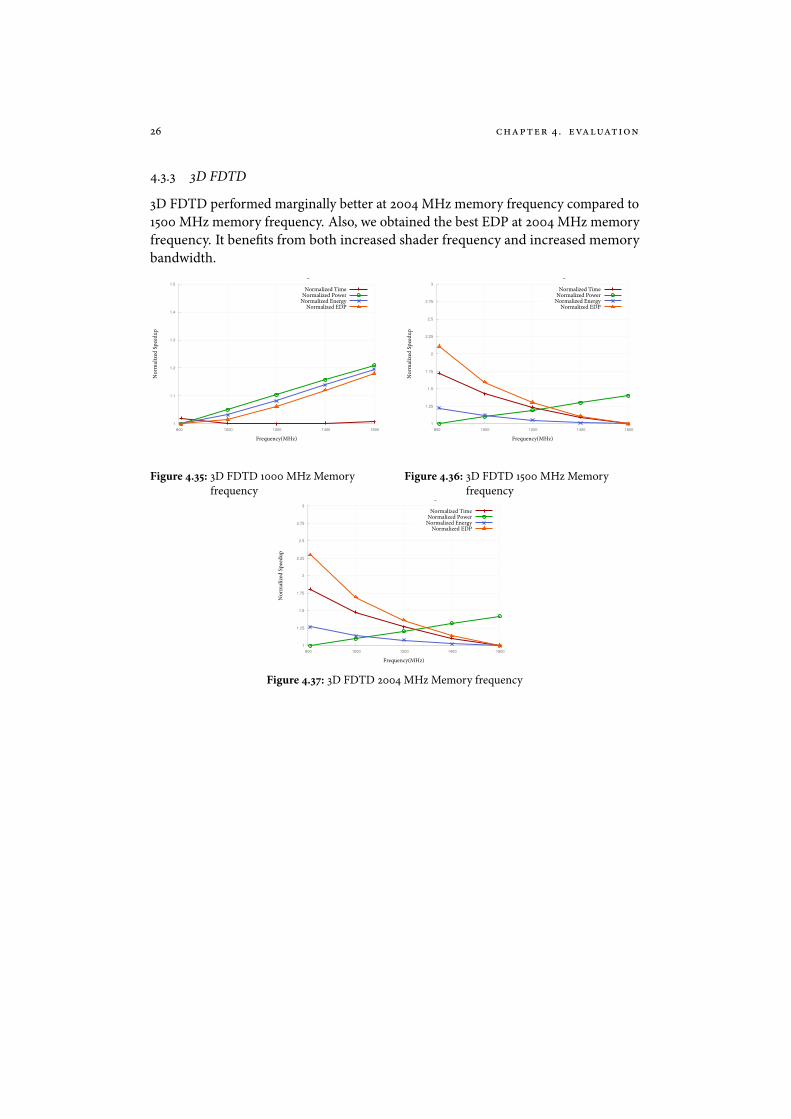
4.3.3 3D FDTD
3D FDTD performed marginally better at 2004 MHz memory frequency compared to1500 MHz memory frequency. Also, we obtained the best EDP at 2004 MHz memoryfrequency. It bene�ts from both increased shader frequency and increased memorybandwidth.
1
1.1
1.2
1.3
1.4
1.5
800 1000 1200 1400 1600
Nor
mal
ized
Spe
edup
Frequency(MHz)
Normalized Power Profiling
Normalized TimeNormalized Power
Normalized EnergyNormalized EDP
Figure 4.35: 3D FDTD 1000 MHz Memoryfrequency
1
1.25
1.5
1.75
2
2.25
2.5
2.75
3
800 1000 1200 1400 1600
Nor
mal
ized
Spe
edup
Frequency(MHz)
Normalized Power Profiling
Normalized TimeNormalized Power
Normalized EnergyNormalized EDP
Figure 4.36: 3D FDTD 1500 MHz Memoryfrequency
1
1.25
1.5
1.75
2
2.25
2.5
2.75
3
800 1000 1200 1400 1600
Nor
mal
ized
Spe
edup
Frequency(MHz)
Normalized Power Profiling
Normalized TimeNormalized Power
Normalized EnergyNormalized EDP
Figure 4.37: 3D FDTD 2004 MHz Memory frequency

4.3 . memory bandwidth 27
4.3.4 Scalar Product
Scalar product benchmark performs better at 2004 MHz memory frequency. It is amemory bound benchmark and bene�ts from higher memory bandwidth. Also, thebest EDP value was obtained at 2004 MHz memory frequency.
1
1.1
1.2
1.3
1.4
1.5
800 1000 1200 1400 1600
Nor
mal
ized
Spe
edup
Frequency(MHz)
Normalized Power Profiling
Normalized TimeNormalized Power
Normalized EnergyNormalized EDP
Figure 4.38: Scalar product 1000 MHz Memoryfrequency
1
1.1
1.2
1.3
1.4
1.5
800 1000 1200 1400 1600
Nor
mal
ized
Spe
edup
Frequency(MHz)
Normalized Power Profiling
Normalized TimeNormalized Power
Normalized EnergyNormalized EDP
Figure 4.39: Scalar product 1500 MHz Memoryfrequency
1
1.2
1.4
1.6
1.8
2
800 1000 1200 1400 1600
Nor
mal
ized
Spe
edup
Frequency(MHz)
Normalized Power Profiling
Normalized TimeNormalized Power
Normalized EnergyNormalized EDP
Figure 4.40: Scalar product 2004 MHz Memory frequency


chapter 5
Conclusion
In this thesis work we have evaluated the application of DVFS on GPU for generalpurpose workloads. From the results we have from the microbenchmark evaluation,we can conclude that DVFS can be e�ectively applied to memory bound kernels. Wealso show how the number of warps(threads) also a�ect the performance and power ofa kernel. For higher memory bound applications it is more suitable to have fewer warpsto get better performance and lower power. �e benchmarks we evaluated showed thebest EDP at the highest shader frequency. But it would be interesting to investigate theimpact of warp sizes on their performance and power. Also, we evaluated the powerand performance of some of the benchmarks at di�erent memory bandwidths. Certaincompute intensive benchmarks are not signi�cantly a�ected by reducing the memorybandwidth and it saves some power.
We have also provided the infrastructure to accurately measure the GPU powerconsumption from each power source. At the very end of the thesis work the Graphiccard broke due to excessive DVFS. So, it might not be advisable to do DVFS on currentdesktop grade hardware.
nVidia has been making it easier to pro�le the GPU kernels. As a part of future work,my thesis data can be used along with the pro�ler data to make power models[8][4][3]for DVFS in GPUs.
29


B iblio graphy
[1] J.Y. Chen. “GPU technology trends and future requirements”. In: ElectronDevices Meeting (IEDM), 2009 IEEE International. IEEE. 2009, pp. 1–6.
[2] J.L. Hennessy and D.A. Patterson. Computer architecture: a quantitative ap-proach. 5th ed. Morgan Kaufmann Pub, 2012.
[3] S. Hong and H. Kim. “An integrated GPU power and performance model”. In:ACM SIGARCH Computer Architecture News. Vol. 38. 3. ACM. 2010, pp. 280–289.
[4] Sunpyo Hong and Hyesoon Kim. “An analytical model for a GPU architecturewith memory-level and thread-level parallelism awareness”. In: Proceedingsof the 36th annual international symposium on Computer architecture. ISCA’09. Austin, TX, USA: ACM, 2009, pp. 152–163. isbn: 978-1-60558-526-0. doi:10.1145/1555754.1555775. url: http://doi.acm.org/10.1145/1555754.1555775.
[5] Y. Jiao et al. “Power and performance characterization of computational ker-nels on the GPU”. In: Green Computing and Communications (GreenCom),2010 IEEE/ACM Int’l Conference on & Int’l Conference on Cyber, Physical andSocial Computing (CPSCom). IEEE. 2010, pp. 221–228.
[6] Stefanos Kaxiras and Margaret Martonosi. Computer Architecture Techniquesfor Power-E�ciency. 1st. Morgan and Claypool Publishers, 2008. isbn: 1598292080,9781598292084.
[7] T. Mudge. “Power: A �rst class design constraint for future architectures”. In:High Performance Computing HiPC 2000 (2000), pp. 215–224.
[8] H. Nagasaka et al. “Statistical power modeling of GPU kernels using perfor-mance counters”. In: Green Computing Conference, 2010 International. IEEE.2010, pp. 115–122.
[9] “Nvidia CUDA C programming guide version 4.2”. In: (2012).
[10] M. Scott. Upgrading and repairing PCs. Que Publishing, 2011.
[11] J. A. Stratton et al. Parboil Benchmarks. http://impact.crhc.illinois.edu/Parboil/parboil.aspx. [Online; accessed 6-May-2012]. 2012.
31
32 biblio graphy
[12] R. Suda and D.Q. Ren. “Accurate Measurements and Precise Modeling ofPower Dissipation of CUDA Kernels toward Power Optimized High Perfor-mance CPU-GPU Computing”. In: 2009 International Conference on Paral-lel and Distributed Computing, Applications and Technologies. IEEE. 2009,pp. 432–438.
[13] CUDA SDK V4.2. http://developer.nvidia.com/gpu-computing-sdk.[Online; accessed 24-April-2012]. 2012.
[14] CUDA TOOLKIT V4.2. http://developer.nvidia.com/cuda-toolkit.[Online; accessed 24-April-2012]. 2012.
[15] Whitepaper , NVIDIA’s next generation CUDA compute architecture: Fermi.http://www.nvidia.com/content/PDF/fermi_white_papers/NVIDIA_
Fermi_Compute_Architecture_Whitepaper.pdf. v1.1, [Online; accessed6-May-2012]. 2009.
Assembly code
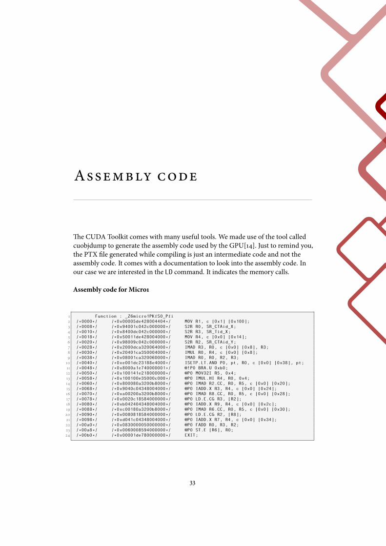
�e CUDA Toolkit comes with many useful tools. We made use of the tool calledcuobjdump to generate the assembly code used by the GPU[14]. Just to remind you,the PTX �le generated while compiling is just an intermediate code and not theassembly code. It comes with a documentation to look into the assembly code. Inour case we are interested in the LD command. It indicates the memory calls.
Assembly code for Micro1
1 Function : _Z6micro1PKfS0_Pfi
2 /*0000*/ /*0x00005de428004404*/ MOV R1, c [0x1] [0x100];
3 /*0008*/ /*0x94001c042c000000*/ S2R R0, SR_CTAid_X;
4 /*0010*/ /*0x8400dc042c000000*/ S2R R3, SR_Tid_X;
5 /*0018*/ /*0x50011de428004000*/ MOV R4, c [0x0] [0x14];
6 /*0020*/ /*0x98009c042c000000*/ S2R R2, SR_CTAid_Y;
7 /*0028*/ /*0x2000dca320064000*/ IMAD R3, R0, c [0x0] [0x8], R3;
8 /*0030*/ /*0x20401ca350004000*/ IMUL R0, R4, c [0x0] [0x8];
9 /*0038*/ /*0x08001ca320060000*/ IMAD R0, R0, R2, R3;
10 /*0040*/ /*0xe001dc23188e4000*/ ISETP.LT.AND P0, pt, R0, c [0x0] [0x38], pt;
11 /*0048*/ /*0x8000a1e740000001*/ @!P0 BRA.U 0xb0;
12 /*0050*/ /*0x100141e218000000*/ @P0 MOV32I R5, 0x4;
13 /*0058*/ /*0x100100e35000c000*/ @P0 IMUL.HI R4, R0, 0x4;
14 /*0060*/ /*0x800080a3200b8000*/ @P0 IMAD R2.CC, R0, R5, c [0x0] [0x20];
15 /*0068*/ /*0x9040c04348004000*/ @P0 IADD.X R3, R4, c [0x0] [0x24];
16 /*0070*/ /*0xa00200a3200b8000*/ @P0 IMAD R8.CC, R0, R5, c [0x0] [0x28];
17 /*0078*/ /*0x0020c18584000000*/ @P0 LD.E.CG R3, [R2];
18 /*0080*/ /*0xb042404348004000*/ @P0 IADD.X R9, R4, c [0x0] [0x2c];
19 /*0088*/ /*0xc00180a3200b8000*/ @P0 IMAD R6.CC, R0, R5, c [0x0] [0x30];
20 /*0090*/ /*0x0080818584000000*/ @P0 LD.E.CG R2, [R8];
21 /*0098*/ /*0xd041c04348004000*/ @P0 IADD.X R7, R4, c [0x0] [0x34];
22 /*00a0*/ /*0x0830000050000000*/ @P0 FADD R0, R3, R2;
23 /*00a8*/ /*0x0060008594000000*/ @P0 ST.E [R6], R0;
24 /*00b0*/ /*0x00001de780000000*/ EXIT;
33

34 assembly code
Assembly code for Micro21 Function : _Z6micro2PKfS0_S0_S0_Pfi
2 /*0000*/ /*0x00005de428004404*/ MOV R1, c [0x1] [0x100];
3 /*0008*/ /*0x94001c042c000000*/ S2R R0, SR_CTAid_X;
4 /*0010*/ /*0x8400dc042c000000*/ S2R R3, SR_Tid_X;
5 /*0018*/ /*0x50011de428004000*/ MOV R4, c [0x0] [0x14];
6 /*0020*/ /*0x98009c042c000000*/ S2R R2, SR_CTAid_Y;
7 /*0028*/ /*0x2000dca320064000*/ IMAD R3, R0, c [0x0] [0x8], R3;
8 /*0030*/ /*0x20401ca350004000*/ IMUL R0, R4, c [0x0] [0x8];
9 /*0038*/ /*0x08001ca320060000*/ IMAD R0, R0, R2, R3;
10 /*0040*/ /*0x2001dc23188e4001*/ ISETP.LT.AND P0, pt, R0, c [0x0] [0x48], pt;
11 /*0048*/ /*0x8000a1e740000002*/ @!P0 BRA.U 0xf0;
12 /*0050*/ /*0x100301e218000000*/ @P0 MOV32I R12, 0x4;
13 /*0058*/ /*0x100240e35000c000*/ @P0 IMUL.HI R9, R0, 0x4;
14 /*0060*/ /*0x800280a320198000*/ @P0 IMAD R10.CC, R0, R12, c [0x0] [0x20];
15 /*0068*/ /*0x9092c04348004000*/ @P0 IADD.X R11, R9, c [0x0] [0x24];
16 /*0070*/ /*0xa00180a320198000*/ @P0 IMAD R6.CC, R0, R12, c [0x0] [0x28];
17 /*0078*/ /*0x00a2018584000000*/ @P0 LD.E.CG R8, [R10];
18 /*0080*/ /*0xb091c04348004000*/ @P0 IADD.X R7, R9, c [0x0] [0x2c];
19 /*0088*/ /*0xc00080a320198000*/ @P0 IMAD R2.CC, R0, R12, c [0x0] [0x30];
20 /*0090*/ /*0x0061c18584000000*/ @P0 LD.E.CG R7, [R6];
21 /*0098*/ /*0xd090c04348004000*/ @P0 IADD.X R3, R9, c [0x0] [0x34];
22 /*00a0*/ /*0xe00100a320198000*/ @P0 IMAD R4.CC, R0, R12, c [0x0] [0x38];
23 /*00a8*/ /*0x0020818584000000*/ @P0 LD.E.CG R2, [R2];
24 /*00b0*/ /*0xf091404348004000*/ @P0 IADD.X R5, R9, c [0x0] [0x3c];
25 /*00b8*/ /*0x000180a320198001*/ @P0 IMAD R6.CC, R0, R12, c [0x0] [0x40];
26 /*00c0*/ /*0x0041018584000000*/ @P0 LD.E.CG R4, [R4];
27 /*00c8*/ /*0x1c80c00050000000*/ @P0 FADD R3, R8, R7;
28 /*00d0*/ /*0x1091c04348004001*/ @P0 IADD.X R7, R9, c [0x0] [0x44];
29 /*00d8*/ /*0x0830000050000000*/ @P0 FADD R0, R3, R2;
30 /*00e0*/ /*0x1000000050000000*/ @P0 FADD R0, R0, R4;
31 /*00e8*/ /*0x0060008594000000*/ @P0 ST.E [R6], R0;
32 /*00f0*/ /*0x00001de780000000*/ EXIT;
33 .........................................
Assembly code for Micro31 Function : _Z6micro3PKfS0_S0_S0_S0_S0_Pfi
2 /*0000*/ /*0x00005de428004404*/ MOV R1, c [0x1] [0x100];
3 /*0008*/ /*0x94001c042c000000*/ S2R R0, SR_CTAid_X;
4 /*0010*/ /*0x8400dc042c000000*/ S2R R3, SR_Tid_X;
5 /*0018*/ /*0x50011de428004000*/ MOV R4, c [0x0] [0x14];
6 /*0020*/ /*0x98009c042c000000*/ S2R R2, SR_CTAid_Y;
7 /*0028*/ /*0x2000dca320064000*/ IMAD R3, R0, c [0x0] [0x8], R3;
8 /*0030*/ /*0x20401ca350004000*/ IMUL R0, R4, c [0x0] [0x8];
9 /*0038*/ /*0x08001ca320060000*/ IMAD R0, R0, R2, R3;
10 /*0040*/ /*0x6001dc23188e4001*/ ISETP.LT.AND P0, pt, R0, c [0x0] [0x58], pt;
11 /*0048*/ /*0x8000a1e740000003*/ @!P0 BRA.U 0x130;
12 /*0050*/ /*0x100341e218000000*/ @P0 MOV32I R13, 0x4;
13 /*0058*/ /*0x100300e35000c000*/ @P0 IMUL.HI R12, R0, 0x4;
14 /*0060*/ /*0x800200a3201b8000*/ @P0 IMAD R8.CC, R0, R13, c [0x0] [0x20];
15 /*0068*/ /*0x90c2404348004000*/ @P0 IADD.X R9, R12, c [0x0] [0x24];
16 /*0070*/ /*0xa00180a3201b8000*/ @P0 IMAD R6.CC, R0, R13, c [0x0] [0x28];
17 /*0078*/ /*0x0082418584000000*/ @P0 LD.E.CG R9, [R8];
18 /*0080*/ /*0xb0c1c04348004000*/ @P0 IADD.X R7, R12, c [0x0] [0x2c];
19 /*0088*/ /*0xc00100a3201b8000*/ @P0 IMAD R4.CC, R0, R13, c [0x0] [0x30];
20 /*0090*/ /*0x0063818584000000*/ @P0 LD.E.CG R14, [R6];
21 /*0098*/ /*0xd0c1404348004000*/ @P0 IADD.X R5, R12, c [0x0] [0x34];
22 /*00a0*/ /*0xe00080a3201b8000*/ @P0 IMAD R2.CC, R0, R13, c [0x0] [0x38];
23 /*00a8*/ /*0x0041418584000000*/ @P0 LD.E.CG R5, [R4];
24 /*00b0*/ /*0xf0c0c04348004000*/ @P0 IADD.X R3, R12, c [0x0] [0x3c];
25 /*00b8*/ /*0x000280a3201b8001*/ @P0 IMAD R10.CC, R0, R13, c [0x0] [0x40];
26 /*00c0*/ /*0x0020c18584000000*/ @P0 LD.E.CG R3, [R2];
27 /*00c8*/ /*0x10c2c04348004001*/ @P0 IADD.X R11, R12, c [0x0] [0x44];
28 /*00d0*/ /*0x200180a3201b8001*/ @P0 IMAD R6.CC, R0, R13, c [0x0] [0x48];
29 /*00d8*/ /*0x00a2c18584000000*/ @P0 LD.E.CG R11, [R10];
30 /*00e0*/ /*0x30c1c04348004001*/ @P0 IADD.X R7, R12, c [0x0] [0x4c];
31 /*00e8*/ /*0x0060818584000000*/ @P0 LD.E.CG R2, [R6];
32 /*00f0*/ /*0x3891000050000000*/ @P0 FADD R4, R9, R14;
33 /*00f8*/ /*0x1441000050000000*/ @P0 FADD R4, R4, R5;
34 /*0100*/ /*0x0c40c00050000000*/ @P0 FADD R3, R4, R3;

35
35 /*0108*/ /*0x400100a3201b8001*/ @P0 IMAD R4.CC, R0, R13, c [0x0] [0x50];
36 /*0110*/ /*0x2c30000050000000*/ @P0 FADD R0, R3, R11;
37 /*0118*/ /*0x50c1404348004001*/ @P0 IADD.X R5, R12, c [0x0] [0x54];
38 /*0120*/ /*0x0800000050000000*/ @P0 FADD R0, R0, R2;
39 /*0128*/ /*0x0040008594000000*/ @P0 ST.E [R4], R0;
40 /*0130*/ /*0x00001de780000000*/ EXIT;
Assembly code for Micro41 Function : _Z6micro4PKfS0_S0_S0_S0_S0_S0_S0_S0_S0_Pfi
2 /*0000*/ /*0x00005de428004404*/ MOV R1, c [0x1] [0x100];
3 /*0008*/ /*0x94001c042c000000*/ S2R R0, SR_CTAid_X;
4 /*0010*/ /*0x8400dc042c000000*/ S2R R3, SR_Tid_X;
5 /*0018*/ /*0x50011de428004000*/ MOV R4, c [0x0] [0x14];
6 /*0020*/ /*0x98009c042c000000*/ S2R R2, SR_CTAid_Y;
7 /*0028*/ /*0x2000dca320064000*/ IMAD R3, R0, c [0x0] [0x8], R3;
8 /*0030*/ /*0x20401ca350004000*/ IMUL R0, R4, c [0x0] [0x8];
9 /*0038*/ /*0x08001ca320060000*/ IMAD R0, R0, R2, R3;
10 /*0040*/ /*0xe001dc23188e4001*/ ISETP.LT.AND P0, pt, R0, c [0x0] [0x78], pt;
11 /*0048*/ /*0x8000a1e740000005*/ @!P0 BRA.U 0x1b0;
12 /*0050*/ /*0x100441e218000000*/ @P0 MOV32I R17, 0x4;
13 /*0058*/ /*0x100400e35000c000*/ @P0 IMUL.HI R16, R0, 0x4;
14 /*0060*/ /*0x800280a320238000*/ @P0 IMAD R10.CC, R0, R17, c [0x0] [0x20];
15 /*0068*/ /*0x9102c04348004000*/ @P0 IADD.X R11, R16, c [0x0] [0x24];
16 /*0070*/ /*0xa00200a320238000*/ @P0 IMAD R8.CC, R0, R17, c [0x0] [0x28];
17 /*0078*/ /*0x00a2c18584000000*/ @P0 LD.E.CG R11, [R10];
18 /*0080*/ /*0xb102404348004000*/ @P0 IADD.X R9, R16, c [0x0] [0x2c];
19 /*0088*/ /*0xc00180a320238000*/ @P0 IMAD R6.CC, R0, R17, c [0x0] [0x30];
20 /*0090*/ /*0x0082018584000000*/ @P0 LD.E.CG R8, [R8];
21 /*0098*/ /*0xd101c04348004000*/ @P0 IADD.X R7, R16, c [0x0] [0x34];
22 /*00a0*/ /*0xe00100a320238000*/ @P0 IMAD R4.CC, R0, R17, c [0x0] [0x38];
23 /*00a8*/ /*0x0064818584000000*/ @P0 LD.E.CG R18, [R6];
24 /*00b0*/ /*0xf101404348004000*/ @P0 IADD.X R5, R16, c [0x0] [0x3c];
25 /*00b8*/ /*0x000080a320238001*/ @P0 IMAD R2.CC, R0, R17, c [0x0] [0x40];
26 /*00c0*/ /*0x0042818584000000*/ @P0 LD.E.CG R10, [R4];
27 /*00c8*/ /*0x1100c04348004001*/ @P0 IADD.X R3, R16, c [0x0] [0x44];
28 /*00d0*/ /*0x200300a320238001*/ @P0 IMAD R12.CC, R0, R17, c [0x0] [0x48];
29 /*00d8*/ /*0x0020c18584000000*/ @P0 LD.E.CG R3, [R2];
30 /*00e0*/ /*0x3103404348004001*/ @P0 IADD.X R13, R16, c [0x0] [0x4c];
31 /*00e8*/ /*0x400380a320238001*/ @P0 IMAD R14.CC, R0, R17, c [0x0] [0x50];
32 /*00f0*/ /*0x00c2418584000000*/ @P0 LD.E.CG R9, [R12];
33 /*00f8*/ /*0x5103c04348004001*/ @P0 IADD.X R15, R16, c [0x0] [0x54];
34 /*0100*/ /*0x600180a320238001*/ @P0 IMAD R6.CC, R0, R17, c [0x0] [0x58];
35 /*0108*/ /*0x00e3c18584000000*/ @P0 LD.E.CG R15, [R14];
36 /*0110*/ /*0x7101c04348004001*/ @P0 IADD.X R7, R16, c [0x0] [0x5c];
37 /*0118*/ /*0x800100a320238001*/ @P0 IMAD R4.CC, R0, R17, c [0x0] [0x60];
38 /*0120*/ /*0x0061c18584000000*/ @P0 LD.E.CG R7, [R6];
39 /*0128*/ /*0x9101404348004001*/ @P0 IADD.X R5, R16, c [0x0] [0x64];
40 /*0130*/ /*0xa00300a320238001*/ @P0 IMAD R12.CC, R0, R17, c [0x0] [0x68];
41 /*0138*/ /*0x0041418584000000*/ @P0 LD.E.CG R5, [R4];
42 /*0140*/ /*0xb103404348004001*/ @P0 IADD.X R13, R16, c [0x0] [0x6c];
43 /*0148*/ /*0x00c0818584000000*/ @P0 LD.E.CG R2, [R12];
44 /*0150*/ /*0x20b1000050000000*/ @P0 FADD R4, R11, R8;
45 /*0158*/ /*0x4841000050000000*/ @P0 FADD R4, R4, R18;
46 /*0160*/ /*0x2841000050000000*/ @P0 FADD R4, R4, R10;
47 /*0168*/ /*0x0c40c00050000000*/ @P0 FADD R3, R4, R3;
48 /*0170*/ /*0xc00100a320238001*/ @P0 IMAD R4.CC, R0, R17, c [0x0] [0x70];
49 /*0178*/ /*0x2430c00050000000*/ @P0 FADD R3, R3, R9;
50 /*0180*/ /*0x3c30c00050000000*/ @P0 FADD R3, R3, R15;
51 /*0188*/ /*0x1c30c00050000000*/ @P0 FADD R3, R3, R7;
52 /*0190*/ /*0x1430000050000000*/ @P0 FADD R0, R3, R5;
53 /*0198*/ /*0xd101404348004001*/ @P0 IADD.X R5, R16, c [0x0] [0x74];
54 /*01a0*/ /*0x0800000050000000*/ @P0 FADD R0, R0, R2;
55 /*01a8*/ /*0x0040008594000000*/ @P0 ST.E [R4], R0;
56 /*01b0*/ /*0x00001de780000000*/ EXIT;
57 ...........................................................


Power measurements
Table 1: Microbenchmark 1
Warps Shader Execution Power Energy EDPfrequency(MHz) time (sec) (Watts) (Joules)
16 810 1.882 138.25 260.187 489.6711000 1.560 151.04 235.622 367.5711200 1.382 162.85 225.059 311.0311400 1.254 176.17 220.917 277.0301600 1.172 187.57 219.832 257.643
32 810 1.177 158.79 186.896 219.9761000 0.978 174.19 170.358 166.6101200 0.891 188.19 167.677 149.4001400 0.863 197.68 170.598 147.2261600 0.852 207.56 176.841 150.669
48 810 1.031 166.65 171.816 177.1421000 0.869 183.83 159.748 138.8211200 0.838 195.41 163.754 137.2261400 0.841 204.66 172.119 144.7521600 0.839 210.58 176.677 148.232
37
38 p ower measurements
Table 2: Microbenchmark 2
Warps Shader Execution Power Energy EDPfrequency(MHz) time (sec) (Watts) (Joules)
16 810 2.250 152.09 342.203 769.9561000 1.861 167.69 312.071 580.7641200 1.672 181.99 304.287 508.7681400 1.565 195.26 305.582 478.2361600 1.500 206.39 309.585 464.378
32 810 1.744 171.27 298.695 520.9241000 1.460 189.01 275.955 402.8941200 1.405 201.79 283.515 398.3391400 1.415 211.39 299.117 423.2501600 1.413 221.51 312.994 442.260
48 810 1.781 171.91 306.172 545.2921000 1.499 189.05 283.386 424.7961200 1.422 203.13 288.851 410.7461400 1.423 213.58 303.924 432.4841600 1.419 220.34 312.662 443.668
Table 3: Microbenchmark 3
Warps Shader Execution Power Energy EDPfrequency(MHz) time (sec) (Watts) (Joules)
16 810 2.682 159.51 427.806 1,147.3751000 2.226 176.38 392.622 873.9761200 2.039 191.84 391.162 797.5791400 1.993 203.27 405.117 807.3981600 1.972 214.03 422.067 832.316
32 810 2.542 170.01 432.165 1,098.5641000 2.129 187.98 400.209 852.0461200 2.005 201.68 404.368 810.7591400 1.994 213.29 425.300 848.0491600 1.987 223.03 443.161 880.560
48 810 2.529 171.06 432.611 1,094.0731000 2.110 189.22 399.254 842.426
Continued on next page

39
Continued from previous page
Warps Shader Execution Power Energy EDPfrequency(MHz) time (sec) (Watts) (Joules)1200 2.002 203.28 406.967 814.7471400 1.997 215.21 429.774 858.2591600 1.992 225.49 449.176 894.759
Table 4: Microbenchmark 4
Warps Shader Execution Power Energy EDPfrequency(MHz) time (sec) (Watts) (Joules)
16 810 4.173 163.14 680.783 2,840.9081000 3.455 180.17 622.487 2,150.6941200 3.194 194.97 622.734 1,989.0131400 3.136 207.15 649.622 2,037.2161600 3.099 218.49 677.101 2,098.334
32 810 3.952 174.14 688.201 2,719.7711000 3.284 192.97 633.713 2,081.1151200 3.122 206.05 643.288 2,008.3451400 3.125 218.02 681.313 2,129.1021600 3.118 225.84 704.169 2,195.599
48 810 3.945 172.35 679.921 2,682.2871000 3.278 192.41 630.720 2,067.5001200 3.119 204.84 638.896 1,992.7161400 3.133 218.42 684.310 2,143.9431600 3.128 228.55 714.904 2,236.221
40 p ower measurements
Table 5: Benchmarks at Memory clock 2004 MHz (Data rate 4008 MHz and maximum Bandwidth192.4 GB/s)
Benchmark Shader Execution Power Energy EDPfrequency time (sec) (Watts) (Joules)(MHz)
MatrixMultiplication
810 4.548 131.01 595.833 2,709.8511000 3.696 145.22 536.733 1,983.7661200 3.119 161.51 503.750 1,571.1951400 2.667 177.77 474.113 1,264.4581600 2.351 194.36 456.940 1,074.267
MatrixTranspose
810 1.923 149.96 288.373 554.5411000 1.562 165.45 258.433 403.6721200 1.322 183.22 242.217 320.2111400 1.149 200.55 230.432 264.7661600 1.034 217.65 225.050 232.702
3D FDTD810 1.649 133.74 220.537 363.6661000 1.350 146.91 198.329 267.7431200 1.157 161.31 186.636 215.9371400 1.010 176.62 178.386 180.1701600 0.912 190.19 173.453 158.189
ConjugateGradient
810 0.206 147.02 30.286 6.2391000 0.171 161.94 27.692 4.7351200 0.148 177.31 26.242 3.8841400 0.132 192.72 25.439 3.3581600 0.123 206.82 25.439 3.129
BFS(BreadthFirst Search)
810 0.107 100.17 10.718 1.1471000 0.087 105.68 9.194 0.8001200 0.074 109.35 8.092 0.5991400 0.064 113.73 7.279 0.4661600 0.057 119.27 6.798 0.388
Continued on next page
41
Continued from previous page
Benchmark Shader Execution Power Energy EDPfrequency time (sec) (Watts) (Joules)(MHz)
Radix Sort810 0.934 152.98 142.883 133.4531000 0.762 166.53 126.896 96.6951200 0.642 184.07 118.173 75.8671400 0.551 201.63 111.098 61.2151600 0.505 225.53 113.893 57.516
Histogram810 5.362 134.97 723.709 3,880.5281000 4.341 149.02 646.896 2,808.1751200 3.651 165.18 603.072 2,201.8171400 3.105 182.85 567.749 1,762.8611600 2.726 200.44 546.399 1,489.485
Merge Sort810 4.551 133.84 609.106 2,772.0411000 3.695 146.49 541.281 2,000.0321200 3.136 161.21 505.555 1,585.4191400 2.718 176.39 479.428 1,303.0851600 2.424 191.18 463.420 1,123.331
Eigenvalues810 5.048 98.07 495.057 2,499.0501000 4.094 102.08 417.916 1,710.9461200 3.443 106.86 367.919 1,266.7451400 2.933 111.67 327.528 960.6401600 2.574 116.44 299.717 771.470
Black-Scholes810 16.003 154.32 2,469.583 39,520.7361000 12.971 171.61 2,225.953 28,872.8401200 10.908 191.48 2,088.664 22,783.1451400 9.287 214.39 1,991.040 18,490.7881600 8.163 238.15 1,944.018 15,869.023
ScalarProduct
810 3.674 156.36 574.467 2,110.5901000 3.019 172.03 519.359 1,567.9441200 2.731 188.08 513.646 1,402.7691400 2.562 202.85 519.702 1,331.4761600 2.445 217.85 532.643 1,302.313
42 p ower measurements
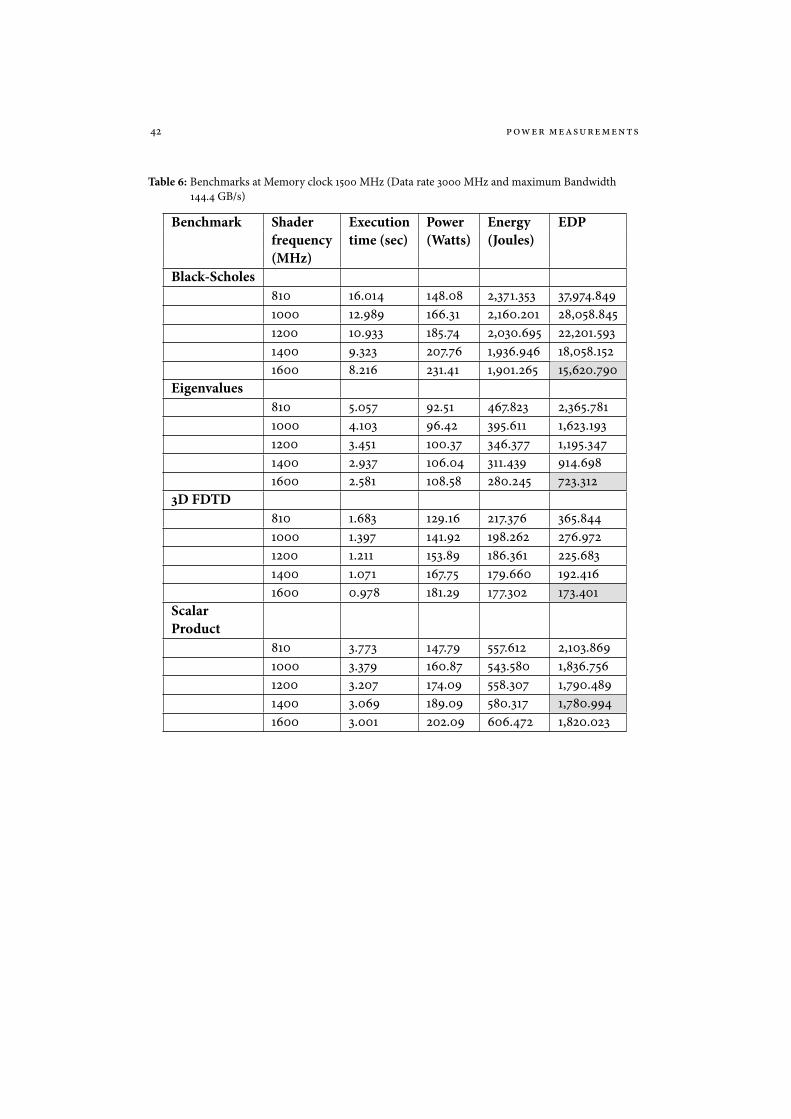
Table 6: Benchmarks at Memory clock 1500 MHz (Data rate 3000 MHz and maximum Bandwidth144.4 GB/s)
Benchmark Shader Execution Power Energy EDPfrequency time (sec) (Watts) (Joules)(MHz)
Black-Scholes810 16.014 148.08 2,371.353 37,974.8491000 12.989 166.31 2,160.201 28,058.8451200 10.933 185.74 2,030.695 22,201.5931400 9.323 207.76 1,936.946 18,058.1521600 8.216 231.41 1,901.265 15,620.790
Eigenvalues810 5.057 92.51 467.823 2,365.7811000 4.103 96.42 395.611 1,623.1931200 3.451 100.37 346.377 1,195.3471400 2.937 106.04 311.439 914.6981600 2.581 108.58 280.245 723.312
3D FDTD810 1.683 129.16 217.376 365.8441000 1.397 141.92 198.262 276.9721200 1.211 153.89 186.361 225.6831400 1.071 167.75 179.660 192.4161600 0.978 181.29 177.302 173.401
ScalarProduct
810 3.773 147.79 557.612 2,103.8691000 3.379 160.87 543.580 1,836.7561200 3.207 174.09 558.307 1,790.4891400 3.069 189.09 580.317 1,780.9941600 3.001 202.09 606.472 1,820.023
43
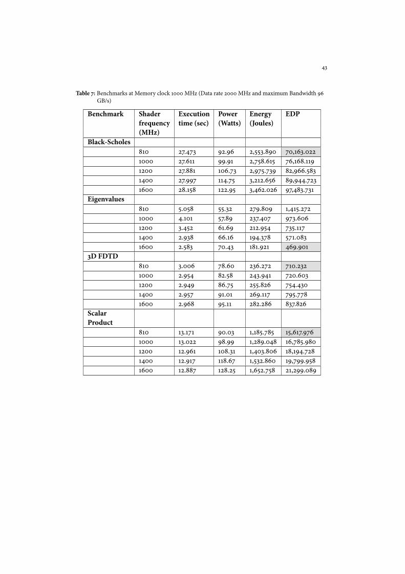
Table 7: Benchmarks at Memory clock 1000 MHz (Data rate 2000 MHz and maximum Bandwidth 96GB/s)
Benchmark Shader Execution Power Energy EDPfrequency time (sec) (Watts) (Joules)(MHz)
Black-Scholes810 27.473 92.96 2,553.890 70,163.0221000 27.611 99.91 2,758.615 76,168.1191200 27.881 106.73 2,975.739 82,966.5831400 27.997 114.75 3,212.656 89,944.7231600 28.158 122.95 3,462.026 97,483.731
Eigenvalues810 5.058 55.32 279.809 1,415.2721000 4.101 57.89 237.407 973.6061200 3.452 61.69 212.954 735.1171400 2.938 66.16 194.378 571.0831600 2.583 70.43 181.921 469.901
3D FDTD810 3.006 78.60 236.272 710.2321000 2.954 82.58 243.941 720.6031200 2.949 86.75 255.826 754.4301400 2.957 91.01 269.117 795.7781600 2.968 95.11 282.286 837.826
ScalarProduct
810 13.171 90.03 1,185.785 15,617.9761000 13.022 98.99 1,289.048 16,785.9801200 12.961 108.31 1,403.806 18,194.7281400 12.917 118.67 1,532.860 19,799.9581600 12.887 128.25 1,652.758 21,299.089
44 p ower measurements
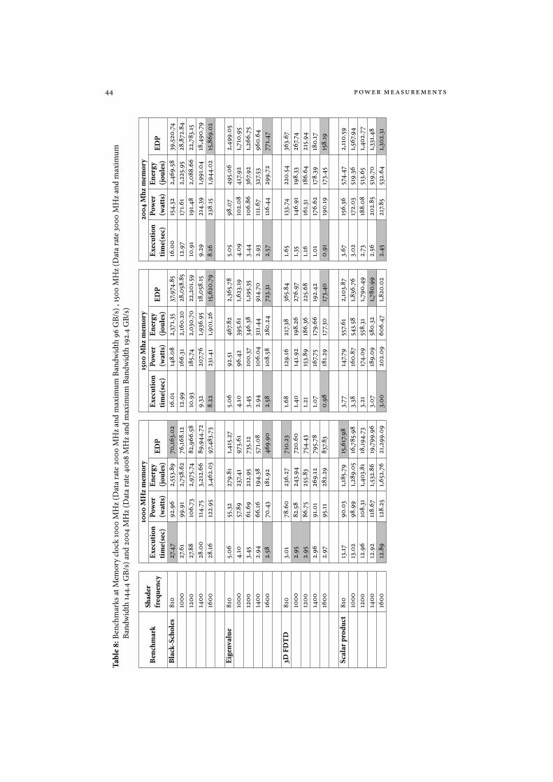
Table8:
Benc
hmar
ksat
Mem
ory
cloc
k10
00M
Hz
(Dat
ara
te20
00M
Hz
and
max
imum
Band
wid
th96
GB/
s),1
500
MH
z(D
ata
rate
3000
MH
zan
dm
axim
umBa
ndw
idth
144.
4G
B/s)
and
2004
MH
z(D
ata
rate
4008
MH
zan
dm
axim
umBa
ndw
idth
192.
4G
B/s)
1000
MHzmem
ory
1500
Mhz
mem
ory
2004
Mhz
mem
ory
Benchmark
Shad
erfrequenc
yEx
ecution
time(sec)
Power
(watts)
Energy
(jou
les)
EDP
Execution
time(sec)
Power
(watts)
Energy
(jou
les)
EDP
Execution
time(sec)
Power
(watts)
Energy
(jou
les)
EDP
Black-Scho
les
810
27.4
792
.96
2,55
3.89
70,16
3.02
16.0
114
8.08
2,37
1.35
37,9
74.8
516
.00
154.
322,
469.
5839
,520.
7410
0027
.61
99.9
12,
758.
6276
,168.
1212
.99
166.
312,
160.
2028
,058
.85
12.9
717
1.61
2,22
5.95
28,8
72.8
412
0027
.88
106.
732,
975.7
482
,966
.5810
.93
185.7
42,
030.
7022
,201
.5910
.91
191.4
82,
088.
6622
,783
.1514
0028
.00
114.
753,2
12.6
689
,944
.72
9.32
207.7
61,9
36.9
518
,058
.159.
2921
4.39
1,991
.04
18,4
90.7
916
0028
.1612
2.95
3,462
.03
97,4
83.7
38.
2223
1.41
1,901
.26
15,6
20.7
98.
1623
8.15
1,944
.02
15,8
69.0
2
Eigenv
alue
810
5.06
55.32
279.
811,4
15.2
75.0
692
.51
467.8
22,
365.7
85.0
598
.07
495.0
62,
499.
0510
004.
1057
.89
237.4
197
3.61
4.10
96.4
239
5.61
1,623
.194.
0910
2.08
417.9
21,7
10.9
512
003.4
561
.69
212.
9573
5.12
3.45
100.
3734
6.38
1,195
.353.4
410
6.86
367.9
21,2
66.7
514
002.
9466
.1619
4.38
571.0
82.
9410
6.04
311.4
491
4.70
2.93
111.6
732
7.53
960.
6416
002.
5870
.43
181.9
246
9.90
2.58
108.
5828
0.24
723.3
12.
5711
6.44
299.
7277
1.47
3DFD
TD
810
3.01
78.6
023
6.27
710.
231.6
812
9.16
217.3
836
5.84
1.65
133.7
422
0.54
363.6
710
002.
9582
.5824
3.94
720.
601.4
014
1.92
198.
2627
6.97
1.35
146.
9119
8.33
267.7
412
002.
9586
.75
255.8
375
4.43
1.21
153.8
918
6.36
225.6
81.1
616
1.31
186.
6421
5.94
1400
2.96
91.0
126
9.12
795.7
81.0
716
7.75
179.
6619
2.42
1.01
176.
6217
8.39
180.
1716
002.
9795
.1128
2.29
837.8
30.
9818
1.29
177.3
017
3.40
0.91
190.
1917
3.45
158.
19
Scalar
prod
uct
810
13.17
90.0
31,1
85.7
915
,617
.98
3.77
147.7
955
7.61
2,10
3.87
3.67
156.
3657
4.47
2,11
0.59
1000
13.0
298
.99
1,289
.05
16,7
85.9
83.3
816
0.87
543.5
81,8
36.7
63.0
217
2.03
519.
361,5
67.9
412
0012
.96
108.
311,4
03.8
118
,194.
733.2
117
4.09
558.
311,7
90.4
92.
7318
8.08
513.6
51,4
02.7
714
0012
.92
118.
671,5
32.8
619
,799
.96
3.07
189.
0958
0.32
1,780
.99
2.56
202.
8551
9.70
1,331
.48
1600
12.8
912
8.25
1,652
.76
21,2
99.0
93.0
020
2.09
606.
471,8
20.0
22.
4521
7.85
532.
641,3
02.31