
gmbyId2
24
Handout #6 B. Murmann Stanford University Winter 2012-13 EE214B g m /I D -Based Design B. Murmann EE214B Winter 2012-13 – HO6 2 Summary on MOSFET Modeling Modern MOSFETs are complicated! The IV-behavior in saturation can be roughly categorized according to the channel’s inversion level: weak, moderate and strong inversion The current is due to diffusion in weak inversion and mostly due to drift in strong inversion; the transition is smooth and complicated The classic square law model is based on an ideal drift model, and applies only near the onset of strong inversion – And even then, the predictions are inaccurate unless short channel effects are taken into account The bottom line is that there is no modeling expression that is simple enough for hand analysis and sufficiently accurate to match real world device behavior
-
Upload
teddy-lesmana -
Category
Documents
-
view
87 -
download
1
description
gmbyId2
Transcript of gmbyId2

Handout #6
B. Murmann
Stanford University
Winter 2012-13
EE214B
gm
/ID-Based Design
B. Murmann EE214B Winter 2012-13 – HO6 2
Summary on MOSFET Modeling
Modern MOSFETs are complicated!
The IV-behavior in saturation can be roughly categorized according to
the channel’s inversion level: weak, moderate and strong inversion
The current is due to diffusion in weak inversion and mostly due to drift
in strong inversion; the transition is smooth and complicated
The classic square law model is based on an ideal drift model, and
applies only near the onset of strong inversion
– And even then, the predictions are inaccurate unless short channel
effects are taken into account
The bottom line is that there is no modeling expression that is simple
enough for hand analysis and sufficiently accurate to match real world
device behavior

B. Murmann EE214B Winter 2012-13 – HO6 3
The Problem
Since there is a disconnect between actual transistor behavior and the
simple square law model, any square-law driven design optimization will
be far off from Spice results
Specifications
Hand Calculations
Circuit
Spice
Results
Square Law
BSIM or PSP
B. Murmann EE214B Winter 2012-13 – HO6 4
Unfortunate Consequence
In absence of a simple set of equations for hand analysis, many
designers tend to converge toward a “spice monkey” design
methodology
– No hand calculations, iterate in spice until the circuit “somehow”
meets the specifications
– Typically results in sub-optimal designs, uninformed design
decisions, etc.
[Courtesy Isaac Martinez]
Our goal
– Maintain a systematic design
methodology in absence of a set of
compact MOSFET equations
Strategy
– Design using look-up tables or charts

B. Murmann EE214B Winter 2012-13 – HO6 5
The Solution
Use pre-computed spice data in hand calculations
B. Murmann EE214B Winter 2012-13 – HO6 6
Starting Point: Technology Characterization via DC Sweep
* /usr/class/ee214b/hspice/techchar.sp
.inc '/usr/class/ee214b/hspice/ee214_hspice.sp'
.inc 'techchar_params.sp'
.param ds = 0.9
.param gs = 0.9
vdsn vdn 0 dc 'ds'
vgsn vgn 0 dc 'gs'
vbsn vbn 0 dc '-subvol'
mn vdn vgn 0 vbn nmos214 L='length' W='width'
.options dccap post brief accurate nomod
.dc gs 0 'gsmax' 'gsstep' ds 0 'dsmax' 'dsstep'
.probe n_id = par('i(mn)')
.probe n_vt = par('vth(mn)')
.probe n_gm = par('gmo(mn)')
.probe n_gmb = par('gmbso(mn)')
.probe n_gds = par('gdso(mn)')
.probe n_cgg = par('cggbo(mn)')
.probe n_cgs = par('-cgsbo(mn)')
.probe n_cgd = par('-cgdbo(mn)')
.probe n_cgb = par('cbgbo(mn)')
.probe n_cdd = par('cddbo(mn)')
.probe n_css = par('cssbo(mn)')
W/L
VGS
-VSB VDS

B. Murmann EE214B Winter 2012-13 – HO6 7
Matlab Wrapper
% /usr/class/ee214b/hspice/techchar.m
% HSpice toolbox
addpath('/usr/class/ee214b/matlab/hspice_toolbox')
% Parameters for HSpice runs
VGS_step = 25e-3; VDS_step = 25e-3; VS_step = 0.1;
VGS_max = 1.8; VDS_max = 1.8; VS_max = 1;
VGS = 0:VGS_step:VGS_max; VDS = 0:VDS_step:VDS_max; VS = 0:VS_step:VS_max;
W = 5; L = [(0.18:0.02:0.5) (0.6:0.1:1.0)];
% HSpice simulation loop
for i = 1:length(L)
for j = 1:length(VS)
% write out circuit parameters and run hspice
fid = fopen('techchar_params.sp', 'w');
fprintf(fid,'*** simulation parameters **** %s\n', datestr(now));
fprintf(fid,'.param width = %d\n', W*1e-6);
fprintf(fid,'.param length = %d\n', L(i)*1e-6);
fprintf(fid,'.param subvol = %d\n', VS(j));
fprintf(fid,'.param gsstep = %d\n', VGS_step);
fprintf(fid,'.param dsstep = %d\n', VDS_step);
fprintf(fid,'.param gsmax = %d\n', VGS_max);
fprintf(fid,'.param dsmax = %d\n', VDS_max);
fclose(fid);
system('/usr/class/ee/synopsys/hspice/F-2011.09-SP2/hspice/bin/hspice techchar.sp >!...
techchar.out');
end
end
B. Murmann EE214B Winter 2012-13 – HO6 8
Simulation Data in Matlab
% data stored in /usr/class/ee214b/matlab
>> load 180nch.mat;
>> nch
nch =
ID: [4-D double]
VT: [4-D double]
GM: [4-D double]
GMB: [4-D double]
GDS: [4-D double]
CGG: [4-D double]
CGS: [4-D double]
CGD: [4-D double]
CGB: [4-D double]
CDD: [4-D double]
CSS: [4-D double]
VGS: [73x1 double]
VDS: [73x1 double]
VS: [11x1 double]
L: [22x1 double]
W: 5
>> size(nch.ID)
ans =
22 73 73 11
, , ,
, , ,
, , ,
…
Four-dimensional arrays

B. Murmann EE214B Winter 2012-13 – HO6 9
Lookup Function (For Convenience)
>> lookup(nch, 'ID', 'VGS', 0.5, 'VDS', 0.5)
ans =
8.4181e-006
>> help lookup
The function "lookup" extracts a desired subset from the 4-dimensional simulation data. The function interpolates when the requested points lie off the simulation grid.
There are three basic usage modes:
(1) Simple lookup of parameters at given (L, VGS, VDS, VS)
(2) Lookup of arbitrary ratios of parameters, e.g. GM_ID, GM_CGG at given(L, VGS, VDS, VS)
(3) Cross-lookup of one ratio against another, e.g. GM_CGG for some GM_ID
In usage scenarios (1) and (2) the input parameters (L, VGS, VDS, VS) can be
listed in any order and default to the following values when not specified:
L = min(data.L); (minimum length used in simulation)
VGS = data.VGS; (VGS vector used during simulation)
VDS = max(data.VDS)/2; (VDD/2)
VS = 0;
B. Murmann EE214B Winter 2012-13 – HO6 10
Key Question
How can we use all this data for systematic design?
Many options exist
– And you can invent your own, if you like
Method taught in EE214B
– Look at the transistor in terms of width-independent figures of merit
that are intimately linked to design specification (rather than some
physical modeling parameters that do not directly relate to circuit
specs)
– Think about the design tradeoffs in terms of the MOSFET’s inversion
level, using gm/ID as a proxy
B. Murmann EE214B Winter 2012-13 – HO6 11
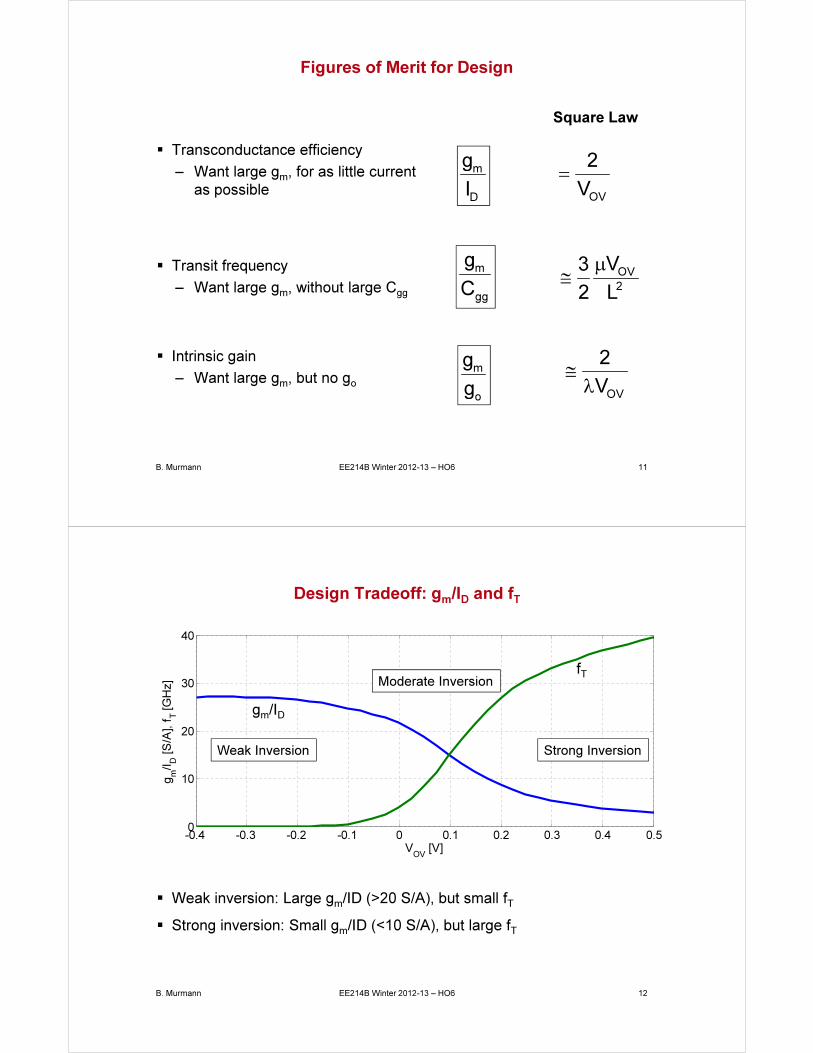
Figures of Merit for Design
Transconductance efficiency
– Want large gm, for as little current
as possible
Transit frequency
– Want large gm, without large Cgg
Intrinsic gain
– Want large gm, but no go
m
D
g
I
m
gg
g
C
m
o
g
g
OV
2
V=
OV
2
V3
2 L
µ≅
Square Law
OV
2
V≅λ
B. Murmann EE214B Winter 2012-13 – HO6 12
Design Tradeoff: gm/ID and fT
Weak inversion: Large gm/ID (>20 S/A), but small fT
Strong inversion: Small gm/ID (<10 S/A), but large fT
-0.4 -0.3 -0.2 -0.1 0 0.1 0.2 0.3 0.4 0.50
10
20
30
40
VOV
[V]
gm
/ID [S
/A], fT [G
Hz]
Weak Inversion Strong Inversion
Moderate InversionfT
gm/ID

B. Murmann EE214B Winter 2012-13 – HO6 13
-0.4 -0.3 -0.2 -0.1 0 0.1 0.2 0.3 0.4 0.50
50
100
150
200
250
VOV
[V]
gm
/ID⋅f T
[S
/A⋅G
Hz]
Product of gm/ID and fT
Interestingly, the product of gm/ID and fT peaks in moderate inversion
Operating the transistor in moderate inversion is optimal when we value
speed and power efficiency equally
– Not always the case
Weak Inversion
Moderate Inversion
Strong Inversion
B. Murmann EE214B Winter 2012-13 – HO6 14
Design in a Nutshell
Choose the inversion level according to the proper tradeoff between
speed (fT) and efficiency (gm/ID) for the given circuit
The inversion level is fully determined by the gate overdrive VOV
– But, VOV is not a very interesting parameter outside the square law
framework; not much can be computed from VOV
ID
gm/ID
B. Murmann EE214B Winter 2012-13 – HO6 15
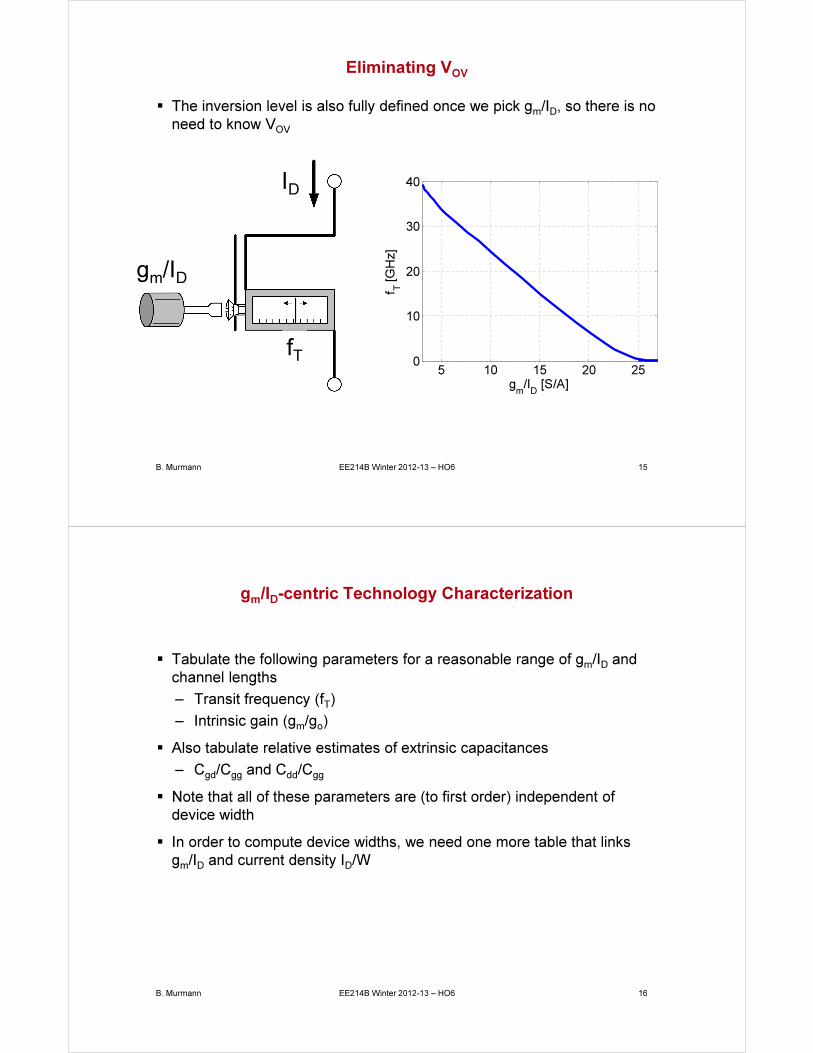
Eliminating VOV
The inversion level is also fully defined once we pick gm/ID, so there is no
need to know VOV
ID
gm/ID
fT
5 10 15 20 250
10
20
30
40
gm
/ID [S/A]
f T [G
Hz]
B. Murmann EE214B Winter 2012-13 – HO6 16
gm/ID-centric Technology Characterization
Tabulate the following parameters for a reasonable range of gm/ID and
channel lengths
– Transit frequency (fT)
– Intrinsic gain (gm/go)
Also tabulate relative estimates of extrinsic capacitances
– Cgd/Cgg and Cdd/Cgg
Note that all of these parameters are (to first order) independent of
device width
In order to compute device widths, we need one more table that links
gm/ID and current density ID/W
B. Murmann EE214B Winter 2012-13 – HO6 17
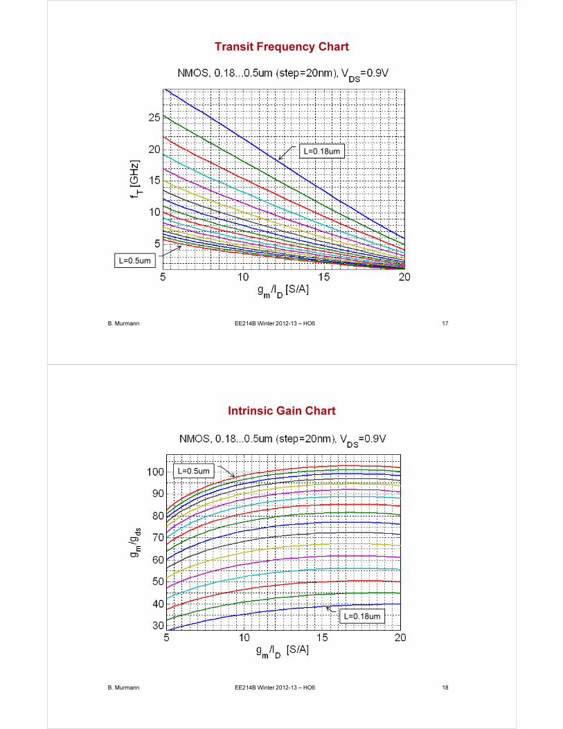
Transit Frequency Chart
L=0.18um
L=0.5um
B. Murmann EE214B Winter 2012-13 – HO6 18
Intrinsic Gain Chart
L=0.18um
L=0.5um
B. Murmann EE214B Winter 2012-13 – HO6 19
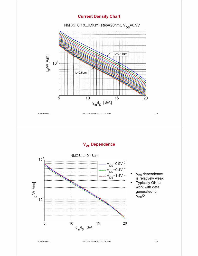
Current Density Chart
L=0.18um
L=0.5um
B. Murmann EE214B Winter 2012-13 – HO6 20
VDS Dependence
VDS dependence
is relatively weak
Typically OK to
work with data
generated for
VDD/2
B. Murmann EE214B Winter 2012-13 – HO6 21
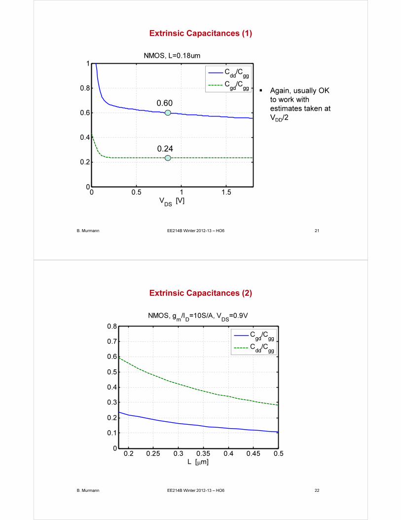
0 0.5 1 1.50
0.2
0.4
0.6
0.8
1NMOS, L=0.18um
VDS
[V]
Cdd
/Cgg
Cgd
/Cgg
Extrinsic Capacitances (1)
Again, usually OK
to work with
estimates taken at
VDD/2
0.60
0.24
B. Murmann EE214B Winter 2012-13 – HO6 22
Extrinsic Capacitances (2)
0.2 0.25 0.3 0.35 0.4 0.45 0.50
0.1
0.2
0.3
0.4
0.5
0.6
0.7
0.8
NMOS, gm
/ID
=10S/A, VDS
=0.9V
L [µm]
Cgd
/Cgg
Cdd
/Cgg

B. Murmann EE214B Winter 2012-13 – HO6 23
Extrinsic Capacitances (3)
0.2 0.25 0.3 0.35 0.4 0.45 0.50
0.1
0.2
0.3
0.4
0.5
0.6
0.7
0.8
PMOS, gm
/ID
=10S/A, VDS
=0.9V
L [µm]
Cgd
/Cgg
Cdd
/Cgg
B. Murmann EE214B Winter 2012-13 – HO6 24
Generic Design Flow
1) Determine gm (from design objectives)
2) Pick L
Short channel high fT (high speed)
Long channel high intrinsic gain
3) Pick gm/ID (or fT)
Large gm/ID low power, large signal swing (low VDSsat)
Small gm/ID high fT (high speed)
4) Determine ID (from gm and gm/ID)
5) Determine W (from ID/W)
Many other possibilities exist (depending on circuit specifics, design
constraints and objectives)

B. Murmann EE214B Winter 2012-13 – HO6 25
0 0.5 1 1.50
0.2
0.4
0.6
VDS
[V]
I D [m
A]
0 0.5 1 1.50
10
20
30
40
VDS
[V]
gm
/gds
How about VDsat?
VDsat tells us how much
voltage we need across the
transistor to operate in
saturation
– “High gain region”
It is important to note that
VDsat is not crisply defined
in modern devices
– Gradual increase of
gm/gds with VDS
VGS=0.9V
VGS=0.8V
VGS=0.7V
VDsat
B. Murmann EE214B Winter 2012-13 – HO6 26
Relationship Between VDsat and gm/ID
It turns out that 2/(gm/ID) is a reasonable first-order estimate for VDsat
( )
( )
( )( )
2
D GS t
m GS t
GS t DSat
m D
I K V V
g 2K V V
2V V V
g / I
= −
= −
= − =
( )
GS t DS
T T
GS t DS
T T
V V V
nV V
D D0
V V V
nV VD0m
T
T T
m D
I I e 1 e
Ig e 1 e
nV
22nV 3V
g / I
−
−
−
−
= −
= −
= ≅
Square Law Weak Inversion
∴Consistent with the classical
first-order relationship
Need about
3VT for
saturation
∴Corresponds well with the
required minimum VDS
B. Murmann EE214B Winter 2012-13 – HO6 27
0 0.5 10
0.2
0.4
0.6
VDS
[V]
I D [m
A]
0 0.5 10
10
20
30
40
VDS
[V]
gm
/gds
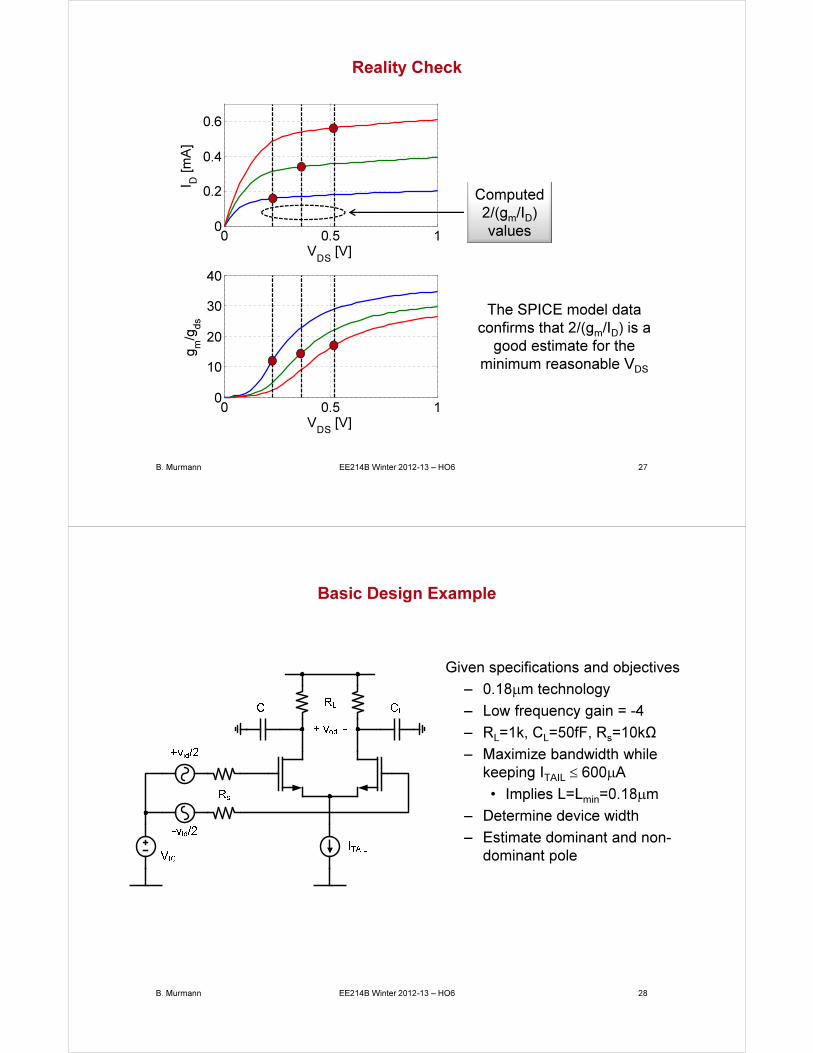
Reality Check
Computed
2/(gm/ID)
values
The SPICE model data
confirms that 2/(gm/ID) is a
good estimate for the
minimum reasonable VDS
B. Murmann EE214B Winter 2012-13 – HO6 28
Basic Design Example
Given specifications and objectives
– 0.18µm technology
– Low frequency gain = -4
– RL=1k, CL=50fF, Rs=10kΩ
– Maximize bandwidth while
keeping ITAIL ≤ 600µA
• Implies L=Lmin=0.18µm
– Determine device width
– Estimate dominant and non-
dominant pole

B. Murmann EE214B Winter 2012-13 – HO6 29
Small-Signal Half-Circuit Model
Calculate gm and gm/ID
v0 m L m
4A g R 4 g 4mS
1k≅ = ⇒ = =
Ω
m
D
g 4mS S13.3
I 300 A A= =
µ
B. Murmann EE214B Winter 2012-13 – HO6 30
Why can we Neglect ro?
Even at L=Lmin= 0.18µm, we have gmro > 30
ro is negligible in this design problem
( )v0 m L o
1
m
L o
v0 m L m o
m L m o
A g R || r
1 1g
R r
1 1 1
A g R g r
1 1 1
4 g R g r
−
=
= +
= +
= +
B. Murmann EE214B Winter 2012-13 – HO6 31
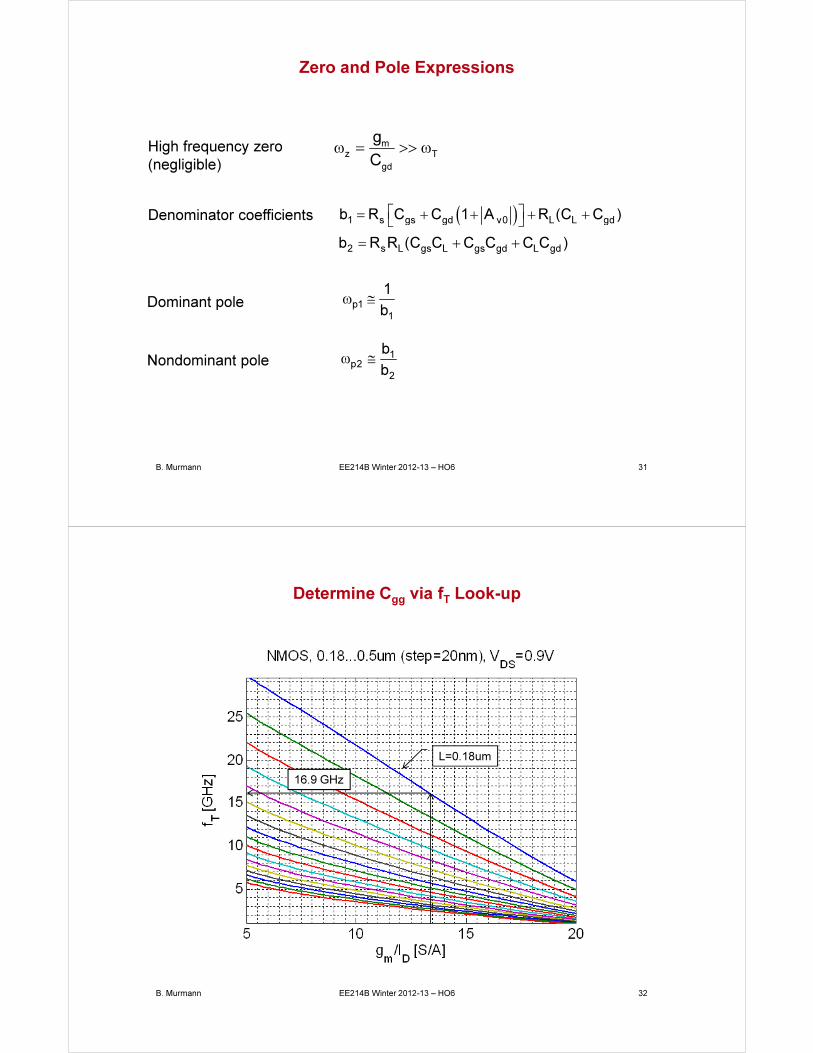
Zero and Pole Expressions
Denominator coefficients
Dominant pole
High frequency zero
(negligible)
mz T
gd
g
Cω = >> ω
( )1 s gs gd v0 L L gdb R C C 1 A R (C C ) = + + + +
2 s L gs L gs gd L gdb R R (C C C C C C )= + +
Nondominant pole
p1
1
1
bω ≅
1p2
2
b
bω ≅
B. Murmann EE214B Winter 2012-13 – HO6 32
Determine Cgg via fT Look-up
L=0.18um
16.9 GHz

B. Murmann EE214B Winter 2012-13 – HO6 33
Find Capacitances and Plug in
=
.= .
=
= . ∙ . = .
=
= . ∙ . = .
≅ ≅ .
= − = .
= − = .
B. Murmann EE214B Winter 2012-13 – HO6 34
Device Sizing
L=0.18um16.1 A/m

B. Murmann EE214B Winter 2012-13 – HO6 35
A Note on Current Density
Designing with current density charts in a normalized, width-independent
space works because
– Current density and gm/ID are independent of W
• ID/W ~ W/W
• gm/ID ~ W/W
– There is a one-to-one mapping from gm/ID to current density
( ) ( )
2
2m D m
ox OV ox
D OV D
1m D m
OV OV
D D
g I g2 1 1 1 1C V C
I V W 2 L L 2 I
g I gf V g V g f
I W I
−
−
= = µ = µ
= = =
Square law:
General case:
B. Murmann EE214B Winter 2012-13 – HO6 36
Matlab Design Script
% gm/ID design example clear all; close all;load 180nch.mat;
% SpecsAv0 = 4; RL = 1e3; CL = 50e-15; Rs = 10e3; ITAIL = 600e-6;
% Component calculationsgm = Av0/RL;gm_id = gm/(ITAIL/2);wT = lookup(nch, 'GM_CGG', 'GM_ID', gm_id);cgd_cgg = lookup(nch, 'CGD_CGG', 'GM_ID', gm_id);cdd_cgg = lookup(nch, 'CDD_CGG', 'GM_ID', gm_id);cgg = gm/wT;cgd = cgd_cgg*cgg;cdd = cdd_cgg*cgg;cdb = cdd - cgd;cgs = cgg - cgd;
% pole calculationsb1 = Rs*(cgs + cgd*(1+Av0))+RL*(CL+cgd);b2 = Rs*RL*(cgs*CL + cgs*cgd + CL*cgd);fp1 = 1/2/pi/b1fp2 = 1/2/pi*b1/b2
% device sizingid_w = lookup(nch, 'ID_W', 'GM_ID', gm_id);w = ITAIL/2 / id_w
B. Murmann EE214B Winter 2012-13 – HO6 37
Circuit For Spice Verification
Device width
Simulation circuit
D
D
300 AIW 18.6 m
I 16.1A /m
W
µ= = = µ
600 A
+ vod -
50fF
+vid/2
-vid/2
1V
50fF
10kΩ
1kΩ
18.6/0.18
B. Murmann EE214B Winter 2012-13 – HO6 38
Circuit Netlist
* gm/id design example
* ee214 device models.include /usr/class/ee214b/hspice/ee214_hspice.sp
vdd vdd 0 1.8vic vic 0 1vid vid 0 ac 1x1 vid vic vip vim balunx2 vod voc vop vom balunrdum vod 0 1gigit t 0 600u
m1 vop vgp t 0 nmos214 w=18.6u l=0.18um2 vom vgm t 0 nmos214 w=18.6u l=0.18ursp vip vgp 10krsm vim vgm 10krlp vop vdd 1krlm vom vdd 1kclp vop 0 50fclm vom 0 50f
.op
.ac dec 100 1e6 1000e9
.pz v(vod) vid
.option post brief accurate
.end

B. Murmann EE214B Winter 2012-13 – HO6 39
xfmr
xfmr
Ideal Balun
Useful for separating CM and DM signal components
Bi-directional, preserves port impedance
Uses ideal, inductorless transformers that work down to DC
Not available in all simulators
=
.subckt balun vdm vcm vp vm
e1 vp vcm transformer vdm 0 2
e2 vcm vm transformer vdm 0 2
.ends balun
B. Murmann EE214B Winter 2012-13 – HO6 40
Simulated DC Operating Point
element 0:m1 0:m2
model 0:nmos214 0:nmos214
region Saturati Saturati
id 300.0000u 300.0000u
vgs 682.4474m 682.4474m
vds 1.1824 1.1824
vbs -317.5526m -317.5526m
vth 564.5037m 564.5037m
vdsat 109.0968m 109.0968m
vod 117.9437m 117.9437m
beta 37.2597m 37.2597m
gam eff 583.8490m 583.8490m
gm 4.0718m 4.0718m
gds 100.9678u 100.9678u
gmb 887.2111u 887.2111u
cdtot 20.8290f 20.8290f
cgtot 37.4805f 37.4805f
cstot 42.2382f 42.2382f
cbtot 31.5173f 31.5173f
cgs 26.7862f 26.7862f
cgd 8.9672f 8.9672f
Design values
gm = 4 mS
Cdd = 22.6 fF
Cgg = 37.8 fF
Cgd = 9.0 fF
Good agreement!

B. Murmann EE214B Winter 2012-13 – HO6 41
HSpice .OP Capacitance Output Variables
cdtot 20.8290f
cgtot 37.4805f
cstot 42.2382f
cbtot 31.5173f
cgs 26.7862f
cgd 8.9672f
cdtot ≡ Cgd + Cdb
cgtot ≡ Cgs + Cgd + Cgb
cstot ≡ Cgs + Csb
cbtot ≡ Cgb + Csb+ Cdb
cgs ≡ Cgs
cgd ≡ Cgd
HSpice (.OP) Corresponding Small Signal
Model Elements
B. Murmann EE214B Winter 2012-13 – HO6 42
106
108
1010
1012
-80
-60
-40
-20
0
20
Frequency [Hz]
Magnitude [dB
]
Simulated AC Response
Calculated values: |Av0|=12 dB (4.0), fp1 = 200 MHz, fp2= 5.8 GHz
5.0 GHz
11.4 dB (3.7)
214 MHz

B. Murmann EE214B Winter 2012-13 – HO6 43
Plotting HSpice Results in Matlab
clear all;close all;addpath('/usr/class/ee214b/matlab/hspice_toolbox');
h = loadsig('gm_id_example1.ac0');lssig(h)
f = evalsig(h,'HERTZ');vod = evalsig(h,'vod');magdb = 20*log10(abs(vod));av0 = abs(vod(1))f3dB = interp1(magdb, f, magdb(1)-3, 'spline')
figure(1);semilogx(f, magdb, 'linewidth', 3);xlabel('Frequency [Hz]');ylabel('Magnitude [dB]');axis([1e6 1e12 -80 20]);grid;
B. Murmann EE214B Winter 2012-13 – HO6 44
Using .pz Analysis
***************************************************
input = 0:vid output = v(vod)
poles (rad/sec) poles ( hertz)
real imag real imag
-1.35289g 0. -215.319x 0.
-31.6307g 0. -5.03418g 0.
zeros (rad/sec) zeros ( hertz)
real imag real imag
445.734g 0. 70.9407g 0
Output
Netlist statement
.pz v(vod) vid

B. Murmann EE214B Winter 2012-13 – HO6 45
Observations
The design is essentially right on target!
– Typical discrepancies are no more than 10-20%, due to VDS
dependencies, finite output resistance, etc.
We accomplished this by using pre-computed spice data in the design
process
Even if discrepancies are more significant, there’s always the possibility
to track down the root causes
– Hand calculations are based on parameters that also exist in Spice,
e.g. gm/ID, fT, etc.
– Different from square law calculations using µCox, VOV, etc.
• Based on artificial parameters that do not exist or have no
significance in the spice model
B. Murmann EE214B Winter 2012-13 – HO6 46
Comparison

B. Murmann EE214B Winter 2012-13 – HO6 47
References
F. Silveira et al. "A gm/ID based methodology for the design of CMOS analog circuits and its application to the synthesis of a silicon-on-insulator micropower OTA," IEEE J. Solid-State Circuits, Sep. 1996, pp. 1314-1319.
D. Foty, M. Bucher, D. Binkley, "Re-interpreting the MOS transistor via the inversion coefficient and the continuum of gms/Id," Proc. Int. Conf. on Electronics, Circuits and Systems, pp. 1179-1182, Sep. 2002.
B. E. Boser, "Analog Circuit Design with Submicron Transistors," IEEE SSCS Meeting, Santa Clara Valley, May 19, 2005, http://www.ewh.ieee.org/r6/scv/ssc/May1905.htm
P. Jespers, The gm/ID Methodology, a sizing tool for low-voltage analog
CMOS Circuits, Springer, 2010.
T. Konishi, K. Inazu, J.G. Lee, M. Natsu, S. Masui, and B. Murmann,
“Optimization of High-Speed and Low-Power Operational
Transconductance Amplifier Using gm/ID Lookup Table Methodology,”
IEICE Trans. Electronics, Vol. E94-C, No.3, Mar. 2011.


