
GLCDC HAL Module Guide - Application Project
28
Application Note R11AN0124EU0101 Rev.1.01 Page 1 of 26 Aug 31, 2017 Renesas Synergy™ Platform GLCDC HAL Module Guide Introduction This module guide will enable you to effectively use a module in your own design. Upon completion of this guide, you will be able to add this module to your own design, configure it correctly for the target application and write code, using the included application project code as a reference and efficient starting point. References to more detailed API descriptions and suggestions of other application projects that illustrate more advanced uses of the module are available in the Renesas Synergy Knowledge Base (as described in the References section at the end of this document), and should be valuable resources for creating more complex designs. The Graphics LCD Controller (GLCDC) HAL module is a high-level API for GLCDC applications and is implemented on r_glcd. The GLCDC HAL module uses the Graphics LCD Driver peripheral on the Synergy MCU. A user-defined callback can be created to handle frame buffer switching and underflow detection. 1. GLCDC HAL Module Features • Supports LCD panels with RGB interface (up to 24 bits) and sync signals (HSYNC, VSYNC and Data Enable optional) • Supports various color formats for input graphics planes (RGB888, ARGB8888, RGB565, ARGB1555, ARGB4444, CLUT8, CLUT4, CLUT1) • Supports the Color Look-Up Table (CLUT) usage for input graphics planes (ARGB8888) with 512 words (32 bits/word) • Supports various color formats for output (RGB888, RGB666, RGB565, Serial RGB888) • Can input two graphics planes on top of the background plane and blend them on the screen • Generates a dot clock to the panel. The clock source is selectable from internal or external (LCD_EXTCLK) • Supports brightness adjustment, contrast adjustment, and gamma correction • Supports GLCDC interrupts to handle frame-buffer switching or underflow detection. Figure 1 GLCDC HAL Module Block Diagram R11AN0124EU0101 Rev.1.01 Aug 31, 2017
Transcript of GLCDC HAL Module Guide - Application Project

Application Note
R11AN0124EU0101 Rev.1.01 Page 1 of 26 Aug 31, 2017
Renesas Synergy™ Platform
GLCDC HAL Module Guide Introduction This module guide will enable you to effectively use a module in your own design. Upon completion of this guide, you will be able to add this module to your own design, configure it correctly for the target application and write code, using the included application project code as a reference and efficient starting point. References to more detailed API descriptions and suggestions of other application projects that illustrate more advanced uses of the module are available in the Renesas Synergy Knowledge Base (as described in the References section at the end of this document), and should be valuable resources for creating more complex designs.
The Graphics LCD Controller (GLCDC) HAL module is a high-level API for GLCDC applications and is implemented on r_glcd. The GLCDC HAL module uses the Graphics LCD Driver peripheral on the Synergy MCU. A user-defined callback can be created to handle frame buffer switching and underflow detection.
1. GLCDC HAL Module Features • Supports LCD panels with RGB interface (up to 24 bits) and sync signals (HSYNC, VSYNC and Data Enable
optional) • Supports various color formats for input graphics planes (RGB888, ARGB8888, RGB565, ARGB1555,
ARGB4444, CLUT8, CLUT4, CLUT1) • Supports the Color Look-Up Table (CLUT) usage for input graphics planes (ARGB8888) with 512 words (32
bits/word) • Supports various color formats for output (RGB888, RGB666, RGB565, Serial RGB888) • Can input two graphics planes on top of the background plane and blend them on the screen • Generates a dot clock to the panel. The clock source is selectable from internal or external (LCD_EXTCLK) • Supports brightness adjustment, contrast adjustment, and gamma correction • Supports GLCDC interrupts to handle frame-buffer switching or underflow detection.
Figure 1 GLCDC HAL Module Block Diagram
R11AN0124EU0101 Rev.1.01
Aug 31, 2017

Renesas Synergy™ Platform GLCDC HAL Module Guide
R11AN0124EU0101 Rev.1.01 Page 2 of 26 Aug 31, 2017
2. GLCDC HAL Module APIs Overview The GLCDC HAL module defines APIs for opening, closing, starting, stopping, and controlling the display of information on an LCD panel. A complete list of the available APIs, an example API call, and a short description of each can be found in the following table. A table of status return values follows the API summary table.
Table 1 GLCDC HAL Module API Summary Function Name Example API Call and Description .open g_display.p_api->open (g_display.p_ctrl, g_display.p_cfg);
Open display device. .close g_display.p_api->close (g_display.p_ctrl);
Close display device. .start g_display.p_api->start(g_display.p_ctrl);
Display start.
.stop g_display.p_api->stop(g_display.p_ctrl); Display stop.
.layerChange g_display.p_api->layerChange(g_display.p_ctrl, g_display.p_cfg, &layercng) Change layer parameters at runtime.
.correction g_display.p_api->correction(g_display.p_ctrl, &display_correction) Color correction.
.clut g_display.p_api->clut(g_display.p_ctrl, &clut, &frame) Set CLUT for display device.
.statusGet g_display.p_api->statusGet(g_display.p_ctrl, &status) Get status for display device.
.versionGet g_display.p_api->versionGet(&version) Retrieve the API version using the version pointer.
Note: For more complete descriptions of operation and definitions for the function data structures, typedefs, defines, API data, API structures and function variables, review the SSP User’s Manual API References for the associated module.
Table 2 Status Return Values
Name Description SSP_SUCCESS API call successful. SSP_ERR_ASSERTION Parameter has invalid value. SSP_ERR_INVALID_ALIGNMENT Memory address must be 64 byte aligned for stride SSP_ERR_INVALID_ARGUMENT Invalid parameter in the argument. SSP_ERR_INVALID_MODE Driver state is not DISPLAY_STATE_DISPLAYING SSP_ERR_HW_LOCKED GLCDCC resource is locked. SSP_ERR_CLOCK_GENERATION Dot clock cannot be generated from clock source. SSP_ERR_INVALID_TIMING_SETTING Invalid panel timing parameter. SSP_ERR_INVALID_LAYER_SETTING Invalid layer setting found. SSP_ERR_INVALID_LAYER_FORMAT Invalid format is specified. SSP_ERR_INVALID_GAMMA_SETTING Invalid gamma correction setting found. SSP_ERR_NOT_OPEN The function call is performed when the driver state is not
equal to DISPLAY_STATE_CLOSED. SSP_ERR_INVALID_UPDATE_TIMING A function call is performed when the GLCDC is updating
register values internally. SSP_ERR_INVALID_MODE Function call is performed when the driver state is not
DISPLAY_STATE_OPENED. SSP_ERR_INVALID_CLUT_ACCESS Illegal CLUT entry or size is specified. p_version The version number.
Renesas Synergy™ Platform GLCDC HAL Module Guide
R11AN0124EU0101 Rev.1.01 Page 3 of 26 Aug 31, 2017
Note: Lower level drivers may return common error codes. Refer to the SSP User’s Manual API References for the associated module for a definition of all relevant status return values.
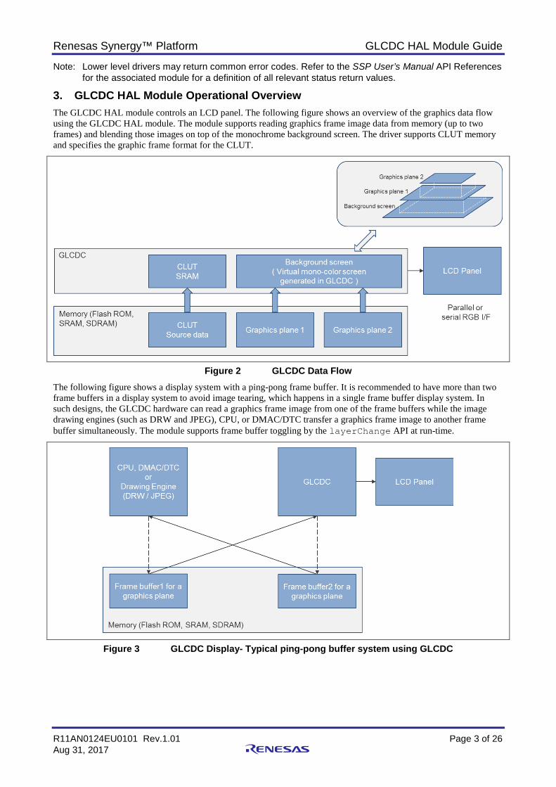
3. GLCDC HAL Module Operational Overview The GLCDC HAL module controls an LCD panel. The following figure shows an overview of the graphics data flow using the GLCDC HAL module. The module supports reading graphics frame image data from memory (up to two frames) and blending those images on top of the monochrome background screen. The driver supports CLUT memory and specifies the graphic frame format for the CLUT.
Figure 2 GLCDC Data Flow The following figure shows a display system with a ping-pong frame buffer. It is recommended to have more than two frame buffers in a display system to avoid image tearing, which happens in a single frame buffer display system. In such designs, the GLCDC hardware can read a graphics frame image from one of the frame buffers while the image drawing engines (such as DRW and JPEG), CPU, or DMAC/DTC transfer a graphics frame image to another frame buffer simultaneously. The module supports frame buffer toggling by the layerChange API at run-time.
Figure 3 GLCDC Display- Typical ping-pong buffer system using GLCDC
Renesas Synergy™ Platform GLCDC HAL Module Guide
R11AN0124EU0101 Rev.1.01 Page 4 of 26 Aug 31, 2017
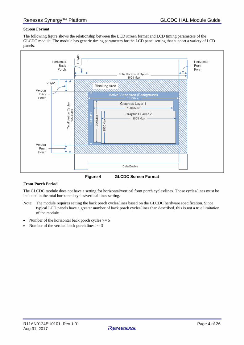
Screen Format
The following figure shows the relationship between the LCD screen format and LCD timing parameters of the GLCDC module. The module has generic timing parameters for the LCD panel setting that support a variety of LCD panels.
Figure 4 GLCDC Screen Format
Front Porch Period
The GLCDC module does not have a setting for horizontal/vertical front porch cycles/lines. Those cycles/lines must be included in the total horizontal cycles/vertical lines setting.
Note: The module requires setting the back porch cycles/lines based on the GLCDC hardware specification. Since typical LCD panels have a greater number of back porch cycles/lines than described, this is not a true limitation of the module.
• Number of the horizontal back porch cycles >= 5 • Number of the vertical back porch lines >= 3

Renesas Synergy™ Platform GLCDC HAL Module Guide
R11AN0124EU0101 Rev.1.01 Page 5 of 26 Aug 31, 2017
Example Parameter Settings
PE-HMI1 v2.0 board (LXD Research & Display, LLC, M7504A)
The following example adjusts the horizontal total cycles, vertical total lines, and panel clock division ratio to generate an LCD panel refresh rate of 60 Hz. Regarding symbols for the LCD panel, see the M7504A data sheet.
Table 3 LCD Panel Parameter Settings — PE-HMI1 v2.0 Board
Renesas Synergy™ Platform GLCDC HAL Module Guide
R11AN0124EU0101 Rev.1.01 Page 6 of 26 Aug 31, 2017
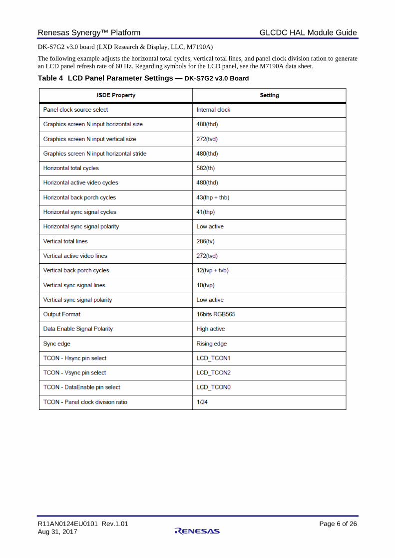
DK-S7G2 v3.0 board (LXD Research & Display, LLC, M7190A)
The following example adjusts the horizontal total cycles, vertical total lines, and panel clock division ration to generate an LCD panel refresh rate of 60 Hz. Regarding symbols for the LCD panel, see the M7190A data sheet.
Table 4 LCD Panel Parameter Settings — DK-S7G2 v3.0 Board
Renesas Synergy™ Platform GLCDC HAL Module Guide
R11AN0124EU0101 Rev.1.01 Page 7 of 26 Aug 31, 2017
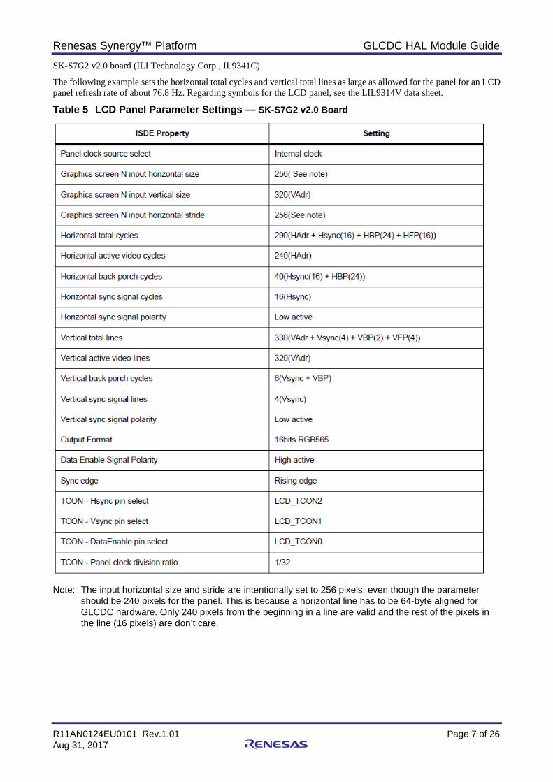
SK-S7G2 v2.0 board (ILI Technology Corp., IL9341C)
The following example sets the horizontal total cycles and vertical total lines as large as allowed for the panel for an LCD panel refresh rate of about 76.8 Hz. Regarding symbols for the LCD panel, see the LIL9314V data sheet.
Table 5 LCD Panel Parameter Settings — SK-S7G2 v2.0 Board
Note: The input horizontal size and stride are intentionally set to 256 pixels, even though the parameter
should be 240 pixels for the panel. This is because a horizontal line has to be 64-byte aligned for GLCDC hardware. Only 240 pixels from the beginning in a line are valid and the rest of the pixels in the line (16 pixels) are don’t care.
Renesas Synergy™ Platform GLCDC HAL Module Guide
R11AN0124EU0101 Rev.1.01 Page 8 of 26 Aug 31, 2017
CLUT
The GLCDC module supports a Color Look-Up table that is used if the color format is ARGB1555, CLUT8, CLUT4, or CLUT1. The CLUT API can update CLUT0/CLUT1 SRAM (implemented inside the GLCDC hardware) for each of the graphics foreground or background screens.
Note: Make sure to call the CLUT API if you select a color format that uses the CLUT, before using the start API. Otherwise, CLUT0 and CLUT1 become an unknown condition and the graphics do not display properly.
You can also call the CLUT API at run-time to update CLUT SRAM.
Note: The API copies the source of CLUT data to the CLUT SRAM, which is not currently used (each CLUT SRAM consists of a ping-pong buffer). After completing the CLUT data update, the API automatically switches the CLUT SRAM to be read by the GLCDC hardware from the next frame to avoid tearing of the image.
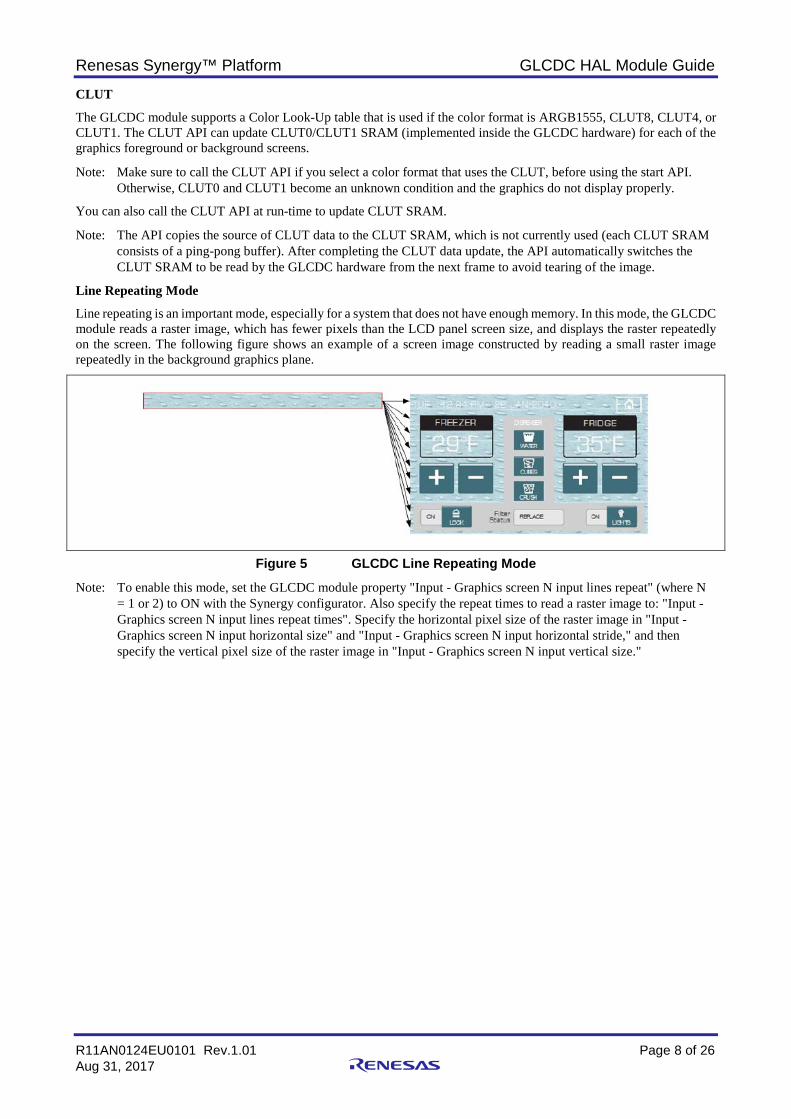
Line Repeating Mode
Line repeating is an important mode, especially for a system that does not have enough memory. In this mode, the GLCDC module reads a raster image, which has fewer pixels than the LCD panel screen size, and displays the raster repeatedly on the screen. The following figure shows an example of a screen image constructed by reading a small raster image repeatedly in the background graphics plane.
Figure 5 GLCDC Line Repeating Mode
Note: To enable this mode, set the GLCDC module property "Input - Graphics screen N input lines repeat" (where N = 1 or 2) to ON with the Synergy configurator. Also specify the repeat times to read a raster image to: "Input - Graphics screen N input lines repeat times". Specify the horizontal pixel size of the raster image in "Input - Graphics screen N input horizontal size" and "Input - Graphics screen N input horizontal stride," and then specify the vertical pixel size of the raster image in "Input - Graphics screen N input vertical size."

Renesas Synergy™ Platform GLCDC HAL Module Guide
R11AN0124EU0101 Rev.1.01 Page 9 of 26 Aug 31, 2017
Gamma Correction
Gamma Correction is used to change the color characteristic of LCD panels to a flat characteristic. The following figure shows the gamma correction curve which can be configured by the GLCDC module. The module supports 16 threshold values for the input color level for each (R, G, B) color and defines the gain level for each of 16 areas divided by thresholds.
Figure 6 GLCDC Gamma Correction Curve
Note: To enable the gamma correction for each channel (R, G, B), set the GLCDC module property "Color correction – Gamma correction (R, G, B)" to ON using the Synergy configurator. Thresholds (total 16) are set to "Color correction – Gamma correction threshold (R, G, B) [n]" where, n = [0…15]. The gain value for each of areas are set to "Color correction – Gamma correction gain (R, G, B) [n]," where, n = [0…15].

Renesas Synergy™ Platform GLCDC HAL Module Guide
R11AN0124EU0101 Rev.1.01 Page 10 of 26 Aug 31, 2017
3.1 GLCDC HAL Module Operational Notes You have the option to configure multiple GLCDC interrupts covered in the following sections.
Line Detection Interrupt
The line-detection interrupt is used to indicate when the GLCDC finishes outputting all lines to the LCD panel and goes into the blanking period. Use this interrupt to handle frame buffer switching in a graphics system and uses frame buffers with more than two frames.
Layer1 or Layer2 Line Buffer Underflow Interrupt
You can use the GLCDC layer1 or layer2 buffer underflow interrupt to detect a lack of memory bandwidth in your system. The buffer underflow occurs when the graphics data transfer from memory (such as the SDRAM or SRAM) to the GLCDC internal line buffer is blocked by another data transfer, and not enough against the data transfer from GLCDC line buffer to the LCD panel interface. You have to design the graphics system to prevent this interrupt from occurring.
GLCDC Callbacks
A user-callback function is registered in the open API call if the user-callback value is not null. If a user-callback function is provided, the callback function is called from the interrupt service routine (ISR) each time an interrupt happens. The argument of the callback function event can take the following enumerated value listed in the table, so that a user can identify which event occurred in the graphics system. The DISPLAY_EVENT_LINE_DETECTION event is used for switching frame buffers to update the screen, and the DISPLAY_EVENT_GRn_UNDERFLOW event is used for error handling if an underflow occurs.
Table 6 Event and Interrupt Summary
Name of Event Name of Interrupt Condition for the Event DISPLAY_EVENT_LINE_DETECTION Line detection When GLCDC is done outputting the
last line in the active video region
DISPLAY_EVENT_GR1_UNDERFLOW Graphics 1 underflow When GLCDC underflows during reading the data for graphics1 plane
DISPLAY_EVENT_GR2_UNDERFLOW Graphics 2 underflow When GLCDC underflows during reading the data for graphics2 plane
Note: Since the callback is called from an ISR, be careful not to use blocking calls or lengthy processing. Spending an excessive time in an ISR can affect the responsiveness of the system.
3.2 GLCDC HAL Module Limitations • The Display driver on r_GLCDC does not support RGB-index chroma key. • The Display driver on r_GLCDC does not support the event-link function.
Refer to the latest SSP Release Notes for any additional operational limitations applicable to this module.

Renesas Synergy™ Platform GLCDC HAL Module Guide
R11AN0124EU0101 Rev.1.01 Page 11 of 26 Aug 31, 2017
4. Including the GLCDC HAL Module in an Application This section describes how to include the GLCDC HAL module in an application using the SSP configurator.
Note: It is assumed that you are familiar with creating a project, adding threads, adding a stack to a thread and configuring a block within the stack. If you are unfamiliar with any of these items, refer to the first few chapters of the SSP User’s Manual to learn how to manage each of these important steps in creating SSP-based applications.
To add the GLCDC HAL module to an application, simply add it to a thread using the stacks selection sequence given in the following table. (The default name for the Display Driver is g_display0. This name can be changed in the associated Properties window.)
Table 7 GLCDC HAL Module Selection Sequence
Resource ISDE Tab Stacks Selection Sequence g_display0 Display Driver on r_glcdc Threads New Stack> Driver> Graphics> Display Driver on
r_glcdc
When the GLCDC HAL module on r_glcdc is added to the thread stack as shown in the following figure, the configurator automatically adds any required lower-level modules. Modules with a Gray band are individual modules that stand alone.
Figure 7 GLCDC HAL Module Stack
5. Configuring the GLCDC HAL Module The GLCDC HAL module must be configured by the user for the desired operation. The SSP configuration window automatically identifies (by highlighting the block in red) any required configuration selections, such as interrupts or operating modes, which must be configured for lower-level modules for successful operation. Furthermore, only those properties that can be changed without causing conflicts are available for modification. Other properties are ‘locked’ and are not available for changes, and are identified with a lock icon for the ‘locked’ property in the Properties window in the ISDE. This approach simplifies the configuration process and makes it much less error-prone than previous ‘manual’ approaches to configuration. The available configuration settings and defaults for all the user-accessible properties are given in the properties tab within the SSP configurator, and are shown in the following tables for easy reference.
One of the properties most often identified as requiring a change is the interrupt priority; this configuration setting is available within the Properties window of the associated module. Simply select the indicated module and then view the properties window; the interrupt settings are often toward the bottom of the properties list, so scroll down until they become available. Also note that the interrupt priorities listed in the Properties window in the ISDE will include an indication as to the validity of the setting based on the targeted MCU (CM4 or CM0+). This level of detail is not included in the following configuration properties tables, but is easily visible with the ISDE when configuring interrupt-priority levels.
Note: You may want to open your ISDE, create the module and explore the property settings in parallel with looking over the following configuration table settings; this helps to orient you and can be a useful hands-on approach to learning the ins and outs of developing with SSP.
Renesas Synergy™ Platform GLCDC HAL Module Guide
R11AN0124EU0101 Rev.1.01 Page 12 of 26 Aug 31, 2017
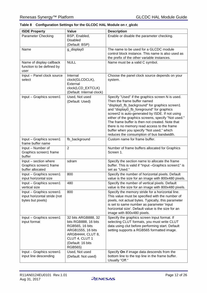
Table 8 Configuration Settings for the GLCDC HAL Module on r_glcdc
ISDE Property Value Description Parameter Checking BSP, Enabled,
Disabled (Default: BSP)
Enable or disable the parameter checking.
Name g_display0 The name to be used for a GLCDC module control block instance. This name is also used as the prefix of the other variable instances.
Name of display callback function to be defined by user
NULL Name must be a valid C symbol.
Input – Panel clock source select
Internal clock(GLCDCLK), External clock(LCD_EXTCLK) (Default: Internal clock)
Choose the panel clock source depends on your system.
Input – Graphics screen1 Used, Not used (Default: Used)
Specify "Used" if the graphics screen N is used. Then the frame buffer named "display0_fb_background" for graphics screen1 and "display0_fb_foreground" for graphics screen2 is auto-generated by ISDE. If not using either of the graphics screens, specify "Not used." The frame buffer is then not created. Note that there is no memory read access to the frame buffer when you specify "Not used," which reduces the consumption of bus bandwidth.
Input – Graphics screen1 frame buffer name
fb_background Custom name for frame buffer.
Input – Number of Graphics screen1 frame buffer
2 Number of frame buffers allocated for Graphics Screen 1.
Input – section where Graphics screen1 frame buffer allocated
sdram Specify the section name to allocate the frame buffer. This is valid if "Input –Graphics screen1" is set as "Used."
Input – Graphics screen1 input horizontal size
800 Specify the number of horizontal pixels. Default value is the size for an image with 800x480 pixels.
Input – Graphics screen1 vertical size
480 Specify the number of vertical pixels. Default value is the size for an image with 800x480 pixels.
Input – Graphics screen1 input horizontal stride (not bytes but pixels)
800 Specify the memory stride for a horizontal line. This value must be specified with the number of pixels, not actual bytes. Typically, this parameter is set to same number as parameter 'input horizontal size'. Default value is the size for an image with 800x480 pixels.
Input – Graphics screen1 input format
32 bits ARGB888, 32 bits RGB888, 16 bits RGB565, 16 bits ARGB1555, 16 bits ARGB4444, CLUT 8, CLUT 4, CLUT 1 (Default: 16 bits RGB565)
Specify the graphics screen Input format. If selecting CLUT formats, you must write CLUT data using clut before performing start. Default setting supports a RGB565 formatted image.
Input – Graphics screen1 input line descending
Used, Not used (Default: Not used)
Specify On if image data descends from the bottom line to the top line in the frame buffer. Usually "Off."

Renesas Synergy™ Platform GLCDC HAL Module Guide
R11AN0124EU0101 Rev.1.01 Page 13 of 26 Aug 31, 2017
ISDE Property Value Description Input – Graphics screen1 input line repeat
On, Off (Default: Off)
Specify On if expecting to repeatedly read a raster image which is smaller than the LCD panel size. Usually Off. For details, see the description of Line Repeating function.
Input – Graphics screen1 input line repeat times
0 Specify the number of repeating times for a raster image which is read repeatedly in a frame.
Input – Graphics screen1 layer coordinate X
0 Specify the horizontal offset in pixels of the graphics screen from the background screen.
Input – Graphics screen1 layer coordinate Y
0 Specify the vertical offset in pixels of the graphics screen from the background screen.
Input – Graphics screen1 layer background color alpha
255 Based on the alpha value, either the graphics screen2 (foreground graphics screen) is blended into the graphics screen1 (background graphics screen) or the graphics screen1 is blended into the monochrome background screen.
Input – Graphics screen1 layer background color Red
255 Specify the background color in the graphics screen N.
Input – Graphics screen1 layer background color Green
255 Specify the background color in the graphics screen N.
Input – Graphics screen1 layer background color Blue
255 Specify the background color in the graphics screen N.
Input – Graphics screen1 layer fading control
None, Fade-in, Fade-out (Default: None)
Specify On when performing a fade-in for the graphics screen. The transparent screen changes gradually to opaque. Specify Off when performing the fade-out for the graphics screen. The opaque screen changes gradually to transparent. Note that this processing is accelerated by the GLCDC hardware and cannot stop once started. The transition status can be monitored by statusGet.
Input – Graphics screen1 layer fade speed
0 Specify the number of frames for the fading transition to complete.
Input – Graphics screen2 Used, Not used (Default: Not used)
Specify Used if the graphics screen N is used. Then the frame buffer named display0_fb_background for graphics screen1 and display0_fb_foreground for graphics screen2 is auto-generated by ISDE. If not using either of the graphics screens, specify Not used. Then, the frame buffer is not created. Note that there is no memory read access to the frame buffer when you specify Not used, which reduces the consumption of bus bandwidth.
Input – Graphics screen2 frame buffer name
fb_foreground Custom name for frame buffer.
Input – Number of Graphics screen2 frame buffer
2 Number of frame buffers allocated for Graphics Screen 2.
Input – section where Graphics screen2 frame buffer allocated
sdram Specify the section name to allocate the frame buffer. This is valid if Input –Graphics screen1 is set as Used.
Input – Graphics screen2 input horizontal size
800 Specify the number of horizontal pixels. Default value is the size for an image with 800x480 pixels.
Input – Graphics screen2 480 Specify the number of vertical pixels. Default

Renesas Synergy™ Platform GLCDC HAL Module Guide
R11AN0124EU0101 Rev.1.01 Page 14 of 26 Aug 31, 2017
ISDE Property Value Description vertical size value is the size for an image with 800x480 pixels. Input – Graphics screen2 input horizontal stride (not bytes but pixels)
800 Specify the memory stride for a horizontal line. This value must be specified with the number of pixels, not actual bytes. Typically, this parameter is set to same number as parameter input horizontal size. Default value is the size for an image with 800x480 pixels.
Input – Graphics screen2 input format
32 bits ARGB888, 32 bits RGB888, 16 bits RGB565, 16 bits ARGB1555, 16 bits ARGB4444, CLUT 8, CLUT 4, CLUT 1 (Default: 16 bits RGB565)
Specify the graphics screen Input format. If selecting CLUT formats, you must write CLUT data using clut before performing start. Default setting supports a RGB565 formatted image.
Input – Graphics screen2 input line descending
On, Off (Default: Off)
Specify On if image data descends from the bottom line to the top line in the frame buffer. Usually Off.
Input – Graphics screen2 input line repeat
On, Off (Default: Off)
Specify On if expecting to repeatedly read a raster image, which is smaller than the LCD panel size. Usually Off. For details, see the description of Line Repeating function.
Input – Graphics screen2 input line repeat times
0 Specify the number of repeating times for a raster image which is read repeatedly in a frame.
Input – Graphics screen2 layer coordinate X
0 Specify the horizontal offset in pixels of the graphics screen from the background screen.
Input – Graphics screen2 layer coordinate Y
0 Specify the vertical offset in pixels of the graphics screen from the background screen.
Input – Graphics screen2 layer background color alpha
255 Based on the alpha value, either the graphics screen2 (foreground graphics screen) is blended into the graphics screen1 (background graphics screen) or the graphics screen1 is blended into the monochrome background screen.
Input – Graphics screen2 layer background color Red
255 Specify the background color in the graphics screen N.
Input – Graphics screen2 layer background color Green
255 Specify the background color in the graphics screen N.
Input – Graphics screen2 layer background color Blue
255 Specify the background color in the graphics screen N.
Input – Graphics screen2 layer fading control
None, Fade-in, Fade-out (Default: None)
Specify On when performing a fade-in for the graphics screen. The transparent screen changes gradually to opaque. Specify Off when performing the fade-out for the graphics screen. The opaque screen changes gradually to transparent. Note that this processing is accelerated by the GLCDC hardware and cannot stop once started. The transition status can be monitored by statusGet.
Input – Graphics screen2 layer fade speed
0 Specify the number of frames for the fading transition to complete.
Output – Horizontal total cycles
1024 Specify the total cycles in a horizontal line. Set to the number of cycles defined in the data sheet of LCD panel sheet in your system. Default value

Renesas Synergy™ Platform GLCDC HAL Module Guide
R11AN0124EU0101 Rev.1.01 Page 15 of 26 Aug 31, 2017
ISDE Property Value Description matches the LCD panel on S7G2 PE-HMI1 board.
Output – Horizontal active video cycles
800 Specify the number of active video cycles in a horizontal line. Set to the number of cycles defined in the data sheet of LCD panel sheet in your system. Default value matches the LCD panel on S7G2 PE-HMI1 board.
Output – Horizontal back porch cycles
46 Specify the number of back porch cycles in a horizontal line. Back porch starts from the beginning of Hsync cycles, which means back porch cycles contain Hsync cycles. Set to the number of cycles defined in the data sheet of LCD panel sheet in your system. Default value matches the LCD panel on S7G2 PE-HMI1 board.
Output – Horizontal sync signal cycles
20 Specify the number of Hsync signal assertion cycles. Set to the number of cycles defined in the data sheet of LCD panel sheet in your system. Default value matches LCD panel on S7G2 PE-HMI1 board.
Output – Horizontal sync signal polarity
Low active, High active (Default: Low active)
Select the polarity of Hsync signal to match your system. Default setting matches the LCD panel on S7G2 PE-HMI1 board.
Output – Vertical total lines
525 Specify number of total lines in a frame. Set to the number of lines defined in the data sheet of LCD panel sheet in your system. Default value matches the LCD panel on S7G2 PE-HMI1 board.
Output – Vertical active video lines
480 Specify the number of active video lines in a frame. Set to the number of lines defined in the data sheet of LCD panel sheet in your system. Default value matches the LCD panel on S7G2 PE-HMI1 board.
Output – Vertical back porch lines
23 Specify the number of back porch lines in a frame. Back porch starts from the beginning of Vsync lines, which means back porch lines contain Vsync lines. Set to the number of lines defined in the data sheet of LCD panel sheet in your system. Default value matches the LCD panel on S7G2 PE-HMI1 board.
Output – Vertical sync signal lines
10 Specify the Vsync signal assertion lines in a frame. Set to the number of lines defined in the data sheet of LCD panel sheet in your system. Default value matches the LCD panel on S7G2 PE-HMI1 board.
Output – Vertical sync signal polarity
Low active, High active (Default: Low active)
Select the polarity of Vsync signal to match to your system. Default setting matches LCD panel on S7G2 PE-HMI1 board.
Output – Format 24 bits RGB888, 18 bits RGB666, 16 bits RGB565, 8 bits serial (Default: 24 bits RGB888)
Specify the graphics screen output format to match to your LCD panel. Default setting matches the LCD panel on S7G2 PE-HMI1 board.
Output – Endian Little endian, Big endian (Default: Little endian)
Select data endian for output signal to LCD panel. Default setting matches the LCD panel on S7G2 PE-HMI1 board.
Output – Color order RGB, BGR (Default: RGB)
Select data order for output signal to LCD panel. The order of blue and red can be swapped if

Renesas Synergy™ Platform GLCDC HAL Module Guide
R11AN0124EU0101 Rev.1.01 Page 16 of 26 Aug 31, 2017
ISDE Property Value Description needed. Default setting matches the LCD panel on S7G2 PE-HMI1 board.
Output – Data Enable Signal Polarity
Low active, High active (Default: High active)
Select the polarity of Data Enable signal to match to your system. Default setting matches the LCD panel on S7G2 PE-HMI1 board.
Output – Sync edge Rising Edge, Falling Edge (Default: Rising Edge)
Select the polarity of Sync signals to match to your system. Default setting matches the LCD panel on S7G2 PE-HMI1 board.
Output – Background color alpha channel
255 Specify the background color of the background screens.
Output – Background color R channel
0 Specify the background color of the background screens.
Output – Background color G channel
0 Specify the background color of the background screens.
Output – Background color B channel
0 Specify the background color of the background screens.
CLUT Used, Not used (Default: Not used)
Specify Used if selecting CLUT formats for a graphics screen input format. Then, a buffer named CLUT_buffer for the CLUT source data is generated in the ISDE auto-generated source file.
CLUT - CLUT buffer size 256 Specify the number of entries for the CLUT source data buffer. Each entry consumes 4 bytes (1 word). Words of CLUT source data specified by this parameter are generated in the ISDE auto-generated source file.
TCON – Hsync pin select Not used, LCD_TCON0, LCD_TCON1, LCD_TCON2, LCD_TCON3 (Default: LCD_TCON0)
Select the TCON pin used for the Hsync signal to match to your system. Default setting is for LCD panel on S7G2 PE-HMI1 board.
TCON – Vsync pin select Not used, LCD_TCON0, LCD_TCON1, LCD_TCON2, LCD_TCON3 (Default: LCD_TCON1)
Select TCON pin used for Vsync signal to match to your system. Default setting is for LCD panel on S7G2 PE-HMI1 board.
TCON – DataEnable pin select
Not used, LCD_TCON0, LCD_TCON1, LCD_TCON2, LCD_TCON3 (Default: LCD_TCON2)
Select TCON pin used for DataEnable signal to match to your system. Default setting is for LCD panel on S7G2 PE-HMI1 board.
TCON – Panel clock division ratio
8-Jan Select the clock source divider value. See the note at bottom of this table about the source clock for the pixel clock.
Color correction – Brightness
Off, On (Default: Off)
Specify On when performing brightness control. If specifying Off, the setting below does not affect the output color.
Color correction – Brightness R channel
512 Output color level is calculated as follows: Output color level = Input color level +/ - 512. Set the value for each R, G, and B channel.
Color correction – Brightness G channel
512 Output color level is calculated as follows: Output color level = Input color level +/ - 512. Set the
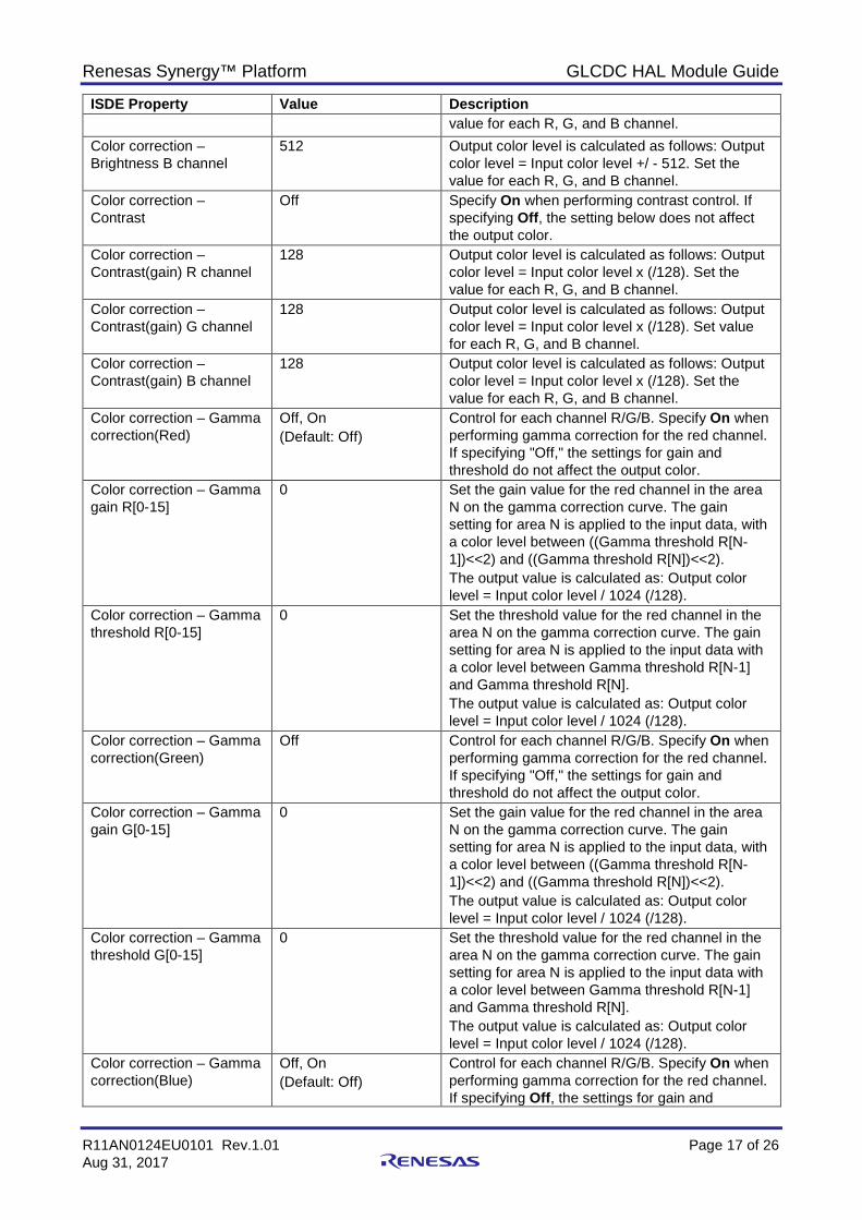
Renesas Synergy™ Platform GLCDC HAL Module Guide
R11AN0124EU0101 Rev.1.01 Page 17 of 26 Aug 31, 2017
ISDE Property Value Description value for each R, G, and B channel.
Color correction – Brightness B channel
512 Output color level is calculated as follows: Output color level = Input color level +/ - 512. Set the value for each R, G, and B channel.
Color correction – Contrast
Off Specify On when performing contrast control. If specifying Off, the setting below does not affect the output color.
Color correction – Contrast(gain) R channel
128 Output color level is calculated as follows: Output color level = Input color level x (/128). Set the value for each R, G, and B channel.
Color correction – Contrast(gain) G channel
128 Output color level is calculated as follows: Output color level = Input color level x (/128). Set value for each R, G, and B channel.
Color correction – Contrast(gain) B channel
128 Output color level is calculated as follows: Output color level = Input color level x (/128). Set the value for each R, G, and B channel.
Color correction – Gamma correction(Red)
Off, On (Default: Off)
Control for each channel R/G/B. Specify On when performing gamma correction for the red channel. If specifying "Off," the settings for gain and threshold do not affect the output color.
Color correction – Gamma gain R[0-15]
0 Set the gain value for the red channel in the area N on the gamma correction curve. The gain setting for area N is applied to the input data, with a color level between ((Gamma threshold R[N-1])<<2) and ((Gamma threshold R[N])<<2). The output value is calculated as: Output color level = Input color level / 1024 (/128).
Color correction – Gamma threshold R[0-15]
0 Set the threshold value for the red channel in the area N on the gamma correction curve. The gain setting for area N is applied to the input data with a color level between Gamma threshold R[N-1] and Gamma threshold R[N]. The output value is calculated as: Output color level = Input color level / 1024 (/128).
Color correction – Gamma correction(Green)
Off Control for each channel R/G/B. Specify On when performing gamma correction for the red channel. If specifying "Off," the settings for gain and threshold do not affect the output color.
Color correction – Gamma gain G[0-15]
0 Set the gain value for the red channel in the area N on the gamma correction curve. The gain setting for area N is applied to the input data, with a color level between ((Gamma threshold R[N-1])<<2) and ((Gamma threshold R[N])<<2). The output value is calculated as: Output color level = Input color level / 1024 (/128).
Color correction – Gamma threshold G[0-15]
0 Set the threshold value for the red channel in the area N on the gamma correction curve. The gain setting for area N is applied to the input data with a color level between Gamma threshold R[N-1] and Gamma threshold R[N]. The output value is calculated as: Output color level = Input color level / 1024 (/128).
Color correction – Gamma correction(Blue)
Off, On (Default: Off)
Control for each channel R/G/B. Specify On when performing gamma correction for the red channel. If specifying Off, the settings for gain and
Renesas Synergy™ Platform GLCDC HAL Module Guide
R11AN0124EU0101 Rev.1.01 Page 18 of 26 Aug 31, 2017
ISDE Property Value Description threshold do not affect the output color.
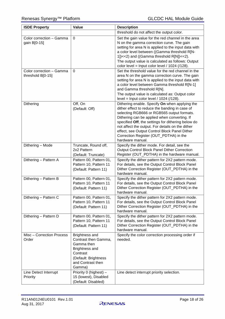
Color correction – Gamma gain B[0-15]
0 Set the gain value for the red channel in the area N on the gamma correction curve. The gain setting for area N is applied to the input data with a color level between ((Gamma threshold R[N-1])<<2) and ((Gamma threshold R[N])<<2). The output value is calculated as follows: Output color level = Input color level / 1024 (/128).
Color correction – Gamma threshold B[0-15]
0 Set the threshold value for the red channel in the area N on the gamma correction curve. The gain setting for area N is applied to the input data with a color level between Gamma threshold R[N-1] and Gamma threshold R[N]. The output value is calculated as: Output color level = Input color level / 1024 (/128).
Dithering Off, On (Default: Off)
Dithering enable. Specify On when applying the dither effect to reduce the banding in case of selecting RGB666 or RGB565 output formats. Dithering can be applied when converting. If specified Off, the settings for dithering below do not affect the output. For details on the dither effect, see Output Control Block Panel Dither Correction Register (OUT_PDTHA) in the hardware manual.
Dithering – Mode Truncate, Round off, 2x2 Pattern (Default: Truncate)
Specify the dither mode. For detail, see the Output Control Block Panel Dither Correction Register (OUT_PDTHA) in the hardware manual.
Dithering – Pattern A Pattern 00, Pattern 01, Pattern 10, Pattern 11 (Default: Pattern 11)
Specify the dither pattern for 2X2 pattern mode. For details, see the Output Control Block Panel Dither Correction Register (OUT_PDTHA) in the hardware manual.
Dithering – Pattern B Pattern 00, Pattern 01, Pattern 10, Pattern 11 (Default: Pattern 11)
Specify the dither pattern for 2X2 pattern mode. For details, see the Output Control Block Panel Dither Correction Register (OUT_PDTHA) in the hardware manual.
Dithering – Pattern C Pattern 00, Pattern 01, Pattern 10, Pattern 11 (Default: Pattern 11)
Specify the dither pattern for 2X2 pattern mode. For details, see the Output Control Block Panel Dither Correction Register (OUT_PDTHA) in the hardware manual.
Dithering – Pattern D Pattern 00, Pattern 01, Pattern 10, Pattern 11 (Default: Pattern 11)
Specify the dither pattern for 2X2 pattern mode. For details, see the Output Control Block Panel Dither Correction Register (OUT_PDTHA) in the hardware manual.
Misc – Correction Process Order
Brightness and Contrast then Gamma, Gamma then Brightness and Contrast (Default: Brightness and Contrast then Gamma)
Specify the color correction processing order if needed.
Line Detect Interrupt Priority
Priority 0 (highest) – 15 (lowest), Disabled (Default: Disabled)
Line detect interrupt priority selection.

Renesas Synergy™ Platform GLCDC HAL Module Guide
R11AN0124EU0101 Rev.1.01 Page 19 of 26 Aug 31, 2017
ISDE Property Value Description Underflow 1 Interrupt Priority
Priority 0 (highest) -15 (lowest), Disabled (Default: Disabled)
Underflow 1 interrupt priority selection.
Underflow 2 Interrupt Priority
Priority 0 (highest) – 15 (lowest), Disabled (Default: Disabled)
Underflow 2 interrupt priority selection.
Note: The example values and defaults are from a project using the Synergy S7G2 Group MCU. Other MCUs may have different default values and different configuration settings available.
5.1 GLCDC HAL Module Clock Configuration The GLCDC module can generate the pixel clock from either of the following clock sources. The source clock selection is available through Synergy Configuration in e2 studio. • Internal clock source (PLLOUT, 240 MHz) • External clock source from the LCD_EXTCLK pin.
Note: The internal clock is different in S7G2 WS1 (Working Sample1) chip and the WS2 (Working Sample2) chip or later. WS1 chip uses PCLKB (max. 60 MHz), but WS2 or later chips use PLLOUT (max. 240 MHz).
5.2 GLCDC HAL Module Pin Configuration The GLCDC module uses pins on the MCU to communicate with external devices. I/O pins must be selected and configured as required by the external device. The pin selection table lists methods to select pins within the SSP configuration window and the configuration settings table lists an example depicting selection of GLCDC pins.
Table 9 Pin Selection Sequence for the GLCDC HAL Module
Resource ISDE Tab Pin selection Sequence GLCDC Pins Select Peripherals > Graphics: GLCDC> GLCDC0
Note: The selection sequence assumes GLCDC0 is the desired hardware target for the driver.
Table 10 Pin Configuration Settings for the GLCDC HAL Module
Property Value Description
Pin Group Selection
Mixed, _A Only, _B Only (Default: Mixed)
Pin group selection
Operation Mode Disabled, Custom, RGB888, RGB666, RGB565 (Default: Disabled)
Select desired operation mode
LCD_CLK None, P900, P101 (Default: None)
LCD_CLK Pin
LCD_DATA00:15
None, Pn, Pm (Default: None)
LCD_DATA Pins
LCD_TCON0:3 None, Pn, Pm (Default: None)
LCD_TCON Pins
LCD_EXTCLK None, Pn, Pm (Default: None)
LCD_EXTCLK Pin
Note: The example values in the table are from a project using the Synergy S7G2 MCU Group and SK-S7G2 Kits. Other Synergy Kits and other Synergy MCUs may have different available pin configuration settings.
Note: To use the GLCDC module on the S7G2 PE-HMI1 board, be sure to set up PORT10 pin 3 (PA03) and pin 5 (PA05) as IOPORT pins with the output level HIGH. Pin PA03 controls the DISP signal (Display on/off) and Pin PA05 controls the backlight of LCD panel. For details, see the schematics of S7G2 PE-HMI1 board.

Renesas Synergy™ Platform GLCDC HAL Module Guide
R11AN0124EU0101 Rev.1.01 Page 20 of 26 Aug 31, 2017
6. Using the GLCD HAL Module in an Application The typical steps in using the GLCDC HAL module in an application are:
1. Initialize the GLCDC HAL module with the open API. 2. Draw a primary image in the frame buffer with application code. 3. Start the image displaying using the start API. 4. Draw a new image in the frame buffer to update the display with application code. Typical user systems consist of
the ping-pong frame buffer system, so draw the image to another frame buffer that is not used for displaying at the point.
5. Request the frame buffer toggling to GLCDC hardware with the layerChange API. 6. The GLCDC hardware toggles the frame buffer and displays a new image from the next frame.
To synchronize the application code with the completion of current frame buffer drawing, use the line-detection interrupt and notify the timing to the application code through the GLCDC callback.
Figure 8 Flow Diagram of a Typical GLCDC HAL Module Application

Renesas Synergy™ Platform GLCDC HAL Module Guide
R11AN0124EU0101 Rev.1.01 Page 21 of 26 Aug 31, 2017
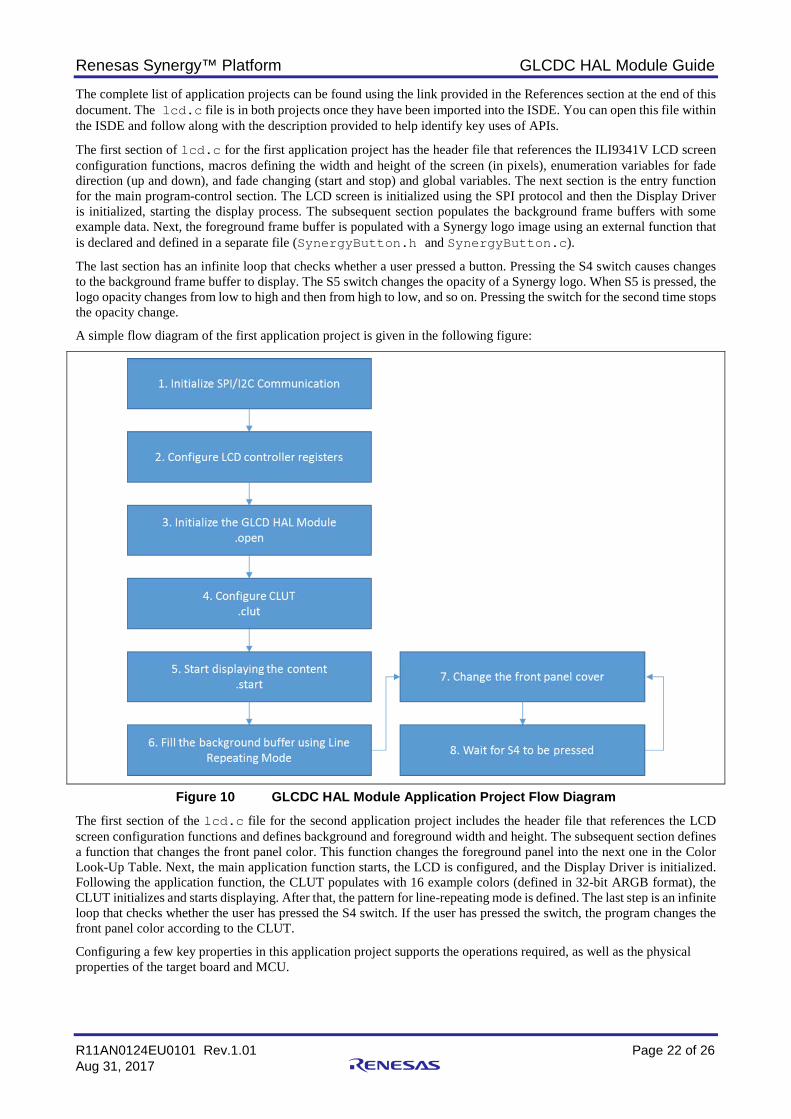
7. The GLCDC HAL Module Application Project The Application Project associated with this Module Guide contains two example projects that demonstrate the aforementioned steps in a full design, and cover the main functions of the GLCD module. The project can be found using the link provided in the References section at the end of this document. You may want to import and open the Application Project within the ISDE and view the configuration settings for the Display Driver module. You can also read over the code, in lcd.c (in both projects) that demonstrates the Display Driver APIs in a complete design.
The application project examples demonstrate the typical use of the Display Driver APIs. Both the application project main thread entries initialize the Display Driver and SPI Communication Driver, which are used to configure the LCD screen controller.
The first application project fills two background buffers with some example data and a foreground buffer with a Synergy logo image. After that occurs, an infinite loop in the program waits for the user to press a button. The S4 button changes the background frame buffer to display, and the S5 button changes the opacity of the Synergy logo foreground by dynamically altering the alpha value of the image. The result is viewed on the LCD panel.
The second application project illustrates the usage of a color look-up table and a line-repeating mode. After initialization of the Display Driver and the LCD configuration through SPI, the CLUT is defined. The table contains 16 colors defined in 32-bit ARGB format. The background pattern is defined, and is used to generate a background image using line-repeating mode. The foreground panel color is then set. At the end, the infinite loop waits for the user to press the S4 button, which changes the panel color.
Table 11 Software and Hardware Resources Used by the Application Project
Resource Revision Description e2 studio 5.3.1 or later Integrated Solution Development Environment SSP 1.2.0 or later Synergy Software™ Platform IAR EW for Synergy 7.71.2 or later IAR Embedded Workbench® for Renesas Synergy™ SSC 5.3.1 or later Synergy Standalone Configurator SK-S7G2 v3.0 to v3.1 Starter Kit
The following figure shows a simple flow diagram depicting the application project:
Figure 9 GLCDC HAL Module Application Project Flow Diagram
Renesas Synergy™ Platform GLCDC HAL Module Guide
R11AN0124EU0101 Rev.1.01 Page 22 of 26 Aug 31, 2017
The complete list of application projects can be found using the link provided in the References section at the end of this document. The lcd.c file is in both projects once they have been imported into the ISDE. You can open this file within the ISDE and follow along with the description provided to help identify key uses of APIs.
The first section of lcd.c for the first application project has the header file that references the ILI9341V LCD screen configuration functions, macros defining the width and height of the screen (in pixels), enumeration variables for fade direction (up and down), and fade changing (start and stop) and global variables. The next section is the entry function for the main program-control section. The LCD screen is initialized using the SPI protocol and then the Display Driver is initialized, starting the display process. The subsequent section populates the background frame buffers with some example data. Next, the foreground frame buffer is populated with a Synergy logo image using an external function that is declared and defined in a separate file (SynergyButton.h and SynergyButton.c).
The last section has an infinite loop that checks whether a user pressed a button. Pressing the S4 switch causes changes to the background frame buffer to display. The S5 switch changes the opacity of a Synergy logo. When S5 is pressed, the logo opacity changes from low to high and then from high to low, and so on. Pressing the switch for the second time stops the opacity change.
A simple flow diagram of the first application project is given in the following figure:
Figure 10 GLCDC HAL Module Application Project Flow Diagram
The first section of the lcd.c file for the second application project includes the header file that references the LCD screen configuration functions and defines background and foreground width and height. The subsequent section defines a function that changes the front panel color. This function changes the foreground panel into the next one in the Color Look-Up Table. Next, the main application function starts, the LCD is configured, and the Display Driver is initialized. Following the application function, the CLUT populates with 16 example colors (defined in 32-bit ARGB format), the CLUT initializes and starts displaying. After that, the pattern for line-repeating mode is defined. The last step is an infinite loop that checks whether the user has pressed the S4 switch. If the user has pressed the switch, the program changes the front panel color according to the CLUT.
Configuring a few key properties in this application project supports the operations required, as well as the physical properties of the target board and MCU.

Renesas Synergy™ Platform GLCDC HAL Module Guide
R11AN0124EU0101 Rev.1.01 Page 23 of 26 Aug 31, 2017
The following table lists key properties along with the values set for this specific project. As a hands-on exercise, you can open the application project and view settings in the Properties window.
Table 12 DTC0 Configuration Settings for the Application Project
ISDE Property Value Set 1st Application Project 2nd Application Project
Name g_display Input – Number of Graphics screen1 frame buffer 2 1 Input – Section where Graphics screen1 frame buffer allocated
bss
Input – Graphics screen1input horizontal size 240 Input – Graphics screen1input vertical size 320 64 Input – Graphics screen1input horizontal stride (not bytes but pixels)
256
Input – Graphic screen1 input lines repeat Off On Input – Graphic screen1 input lines repeat times 0 6 Input – Number of Graphics screen2 frame buffer 1 Input – Section where Graphics screen2 frame buffer allocated
bss
Input – Graphics screen2 input horizontal size 128 Input – Graphics screen2 input vertical size 128 Input – Graphics screen2 input horizontal size (not bytes but pixels)
128
Input – Graphics screen2 input format 32bit ARGB8888 CLUT4 Input – Graphics screen2 layer coordinate X 56 Input – Graphics screen2 layer coordinate Y 96 Output – Horizontal total cycles 320 Output – Horizontal active video cycles 240 Output – Horizontal back porch cycles 6 Output – Horizontal sync signal cycles 4 Output – Vertical total cycles 328 Output – Vertical active video cycles 320 Output – Vertical back porch cycles 4 Output – Vertical sync signal cycles 4 Output – Format 16bit RGB565 CLUT Not used Used CLUT – CLUT buffer size 256 16 TCON – Hsync pin select LCD_TCON2 TCON – DataEnable pin select LCD_TCON0
Make sure to add and configure the SPI Communication stack. The following three tables demonstrate how to add the SPI driver to the stack, configure the connection, and configure the pins.
Table 13 SPI Communication Selection Sequence
Resource ISDE Tab Stacks Selection Sequence g_spi0 SPI Driver on r_sci_spi Threads New Stack> Driver> Connectivity> SPI Driver on
r_sci_spi Note: Observe that the second GLCDC HAL module instance has its interrupt priority set to Disabled. This
setting is necessary because DOC interrupts were enabled by the first instance configuration.
Table 14 SPI Configuration Settings for the Application Project
ISDE Property Value Set Name g_lcd_spi
Renesas Synergy™ Platform GLCDC HAL Module Guide
R11AN0124EU0101 Rev.1.01 Page 24 of 26 Aug 31, 2017
Table 15 Pin Configuration Settings for the Application Project
Pin Selection Sequence Pin Configuration Property Setting Peripherals > Connectivity:SPI > SCI0 Operation Mode Disabled Peripherals > Connectivity:SCI > SCI0 TXD_MOSI P101
TXD_MISO P100 SCK P102
Ports > P6 > P610 Mode Output mode (Initial Low) Ports > P6 > P611 Mode Output mode (Initial Low) Ports > P1 > P615 Mode Output mode (Initial Low)
8. Customizing the GLCDC HAL Module for a Target Application Developers can change some configuration settings from those in the application project. Parameters should be adjusted to the hardware (screen) the user wants to use. Important parameters are those for screen resolution, color space format, timing, in addition to settings for pin configuration (VSYNC, HSYNC, and data enable).
The user may also want to consider using a CLUT, interrupt callbacks, line-repeating mode, multiple render buffers, and other features available through the Display HAL driver.
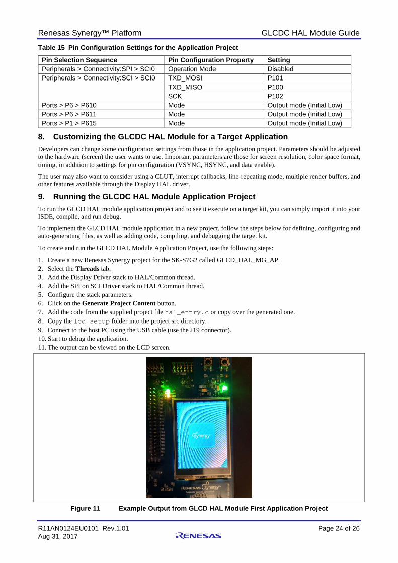
9. Running the GLCDC HAL Module Application Project To run the GLCD HAL module application project and to see it execute on a target kit, you can simply import it into your ISDE, compile, and run debug.
To implement the GLCD HAL module application in a new project, follow the steps below for defining, configuring and auto-generating files, as well as adding code, compiling, and debugging the target kit.
To create and run the GLCD HAL Module Application Project, use the following steps:
1. Create a new Renesas Synergy project for the SK-S7G2 called GLCD_HAL_MG_AP. 2. Select the Threads tab. 3. Add the Display Driver stack to HAL/Common thread. 4. Add the SPI on SCI Driver stack to HAL/Common thread. 5. Configure the stack parameters. 6. Click on the Generate Project Content button. 7. Add the code from the supplied project file hal_entry.c or copy over the generated one. 8. Copy the lcd_setup folder into the project src directory. 9. Connect to the host PC using the USB cable (use the J19 connector). 10. Start to debug the application. 11. The output can be viewed on the LCD screen.
Figure 11 Example Output from GLCD HAL Module First Application Project

Renesas Synergy™ Platform GLCDC HAL Module Guide
R11AN0124EU0101 Rev.1.01 Page 25 of 26 Aug 31, 2017
Figure 12 Example Output from GLCD HAL Module Second Application Project
10. GLCDC HAL Module Conclusion This module guide has provided all the background information needed to select, add, configure, and use the module in an example project. Many of these steps were time consuming and error-prone activities in previous generations of embedded systems. The Renesas Synergy Platform makes these steps much less time consuming and removes the common errors like conflicting configuration settings or the incorrect selection of lower-level modules. The use of high level APIs (as demonstrated in the application project) illustrates additional development-time savings by allowing work to begin at a high level and avoiding the time required in older development environments to use, or, in some cases, create, lower-level drivers.
11. GLCDC HAL Module Next Steps After you have mastered a simple GLCD HAL module project, you may want to review a more complex example. Other application projects and application notes that demonstrate GLCD HAL use are described in the References section.
12. GLCDC HAL Module Reference Information SSP User Manual: Available in html format in the SSP distribution package and as a pdf from the Synergy Gallery.
Links to all the most up-to-date r_glcd module reference materials and resources are available on the Synergy Knowledge Base: https://en-us.knowledgebase.renesas.com/English_Content/Renesas_Synergy%E2%84%A2_Platform/Renesas_Synergy_Knowledge_Base/r_glcd_Module_Guide_Resources.
Renesas Synergy™ Platform GLCDC HAL Module Guide
R11AN0124EU0101 Rev.1.01 Page 26 of 26 Aug 31, 2017
Website and Support Support: https://synergygallery.renesas.com/support
Technical Contact Details:
• America: https://www.renesas.com/en-us/support/contact.html • Europe: https://www.renesas.com/en-eu/support/contact.html • Japan: https://www.renesas.com/ja-jp/support/contact.html
All trademarks and registered trademarks are the property of their respective owners.
Revision History
Rev. Date Description Page Summary
1.00 May 24, 2017 Initial Release 1.01 Aug 31, 2017 Update to Hardware and Software Resources Table

Notice1. Descriptions of circuits, software and other related information in this document are provided only to illustrate the operation of semiconductor products and application examples. You are fully responsible for
the incorporation or any other use of the circuits, software, and information in the design of your product or system. Renesas Electronics disclaims any and all liability for any losses and damages incurred by
you or third parties arising from the use of these circuits, software, or information.
2. Renesas Electronics hereby expressly disclaims any warranties against and liability for infringement or any other disputes involving patents, copyrights, or other intellectual property rights of third parties, by or
arising from the use of Renesas Electronics products or technical information described in this document, including but not limited to, the product data, drawing, chart, program, algorithm, application
examples.
3. No license, express, implied or otherwise, is granted hereby under any patents, copyrights or other intellectual property rights of Renesas Electronics or others.
4. You shall not alter, modify, copy, or otherwise misappropriate any Renesas Electronics product, whether in whole or in part. Renesas Electronics disclaims any and all liability for any losses or damages
incurred by you or third parties arising from such alteration, modification, copy or otherwise misappropriation of Renesas Electronics products.
5. Renesas Electronics products are classified according to the following two quality grades: "Standard" and "High Quality". The intended applications for each Renesas Electronics product depends on the
product’s quality grade, as indicated below.
"Standard": Computers; office equipment; communications equipment; test and measurement equipment; audio and visual equipment; home electronic appliances; machine tools; personal electronic
equipment; and industrial robots etc.
"High Quality": Transportation equipment (automobiles, trains, ships, etc.); traffic control (traffic lights); large-scale communication equipment; key financial terminal systems; safety control equipment; etc.
Renesas Electronics products are neither intended nor authorized for use in products or systems that may pose a direct threat to human life or bodily injury (artificial life support devices or systems, surgical
implantations etc.), or may cause serious property damages (space and undersea repeaters; nuclear power control systems; aircraft control systems; key plant systems; military equipment; etc.). Renesas
Electronics disclaims any and all liability for any damages or losses incurred by you or third parties arising from the use of any Renesas Electronics product for which the product is not intended by Renesas
Electronics.
6. When using the Renesas Electronics products, refer to the latest product information (data sheets, user’s manuals, application notes, "General Notes for Handling and Using Semiconductor Devices" in the
reliability handbook, etc.), and ensure that usage conditions are within the ranges specified by Renesas Electronics with respect to maximum ratings, operating power supply voltage range, heat radiation
characteristics, installation, etc. Renesas Electronics disclaims any and all liability for any malfunctions or failure or accident arising out of the use of Renesas Electronics products beyond such specified
ranges.
7. Although Renesas Electronics endeavors to improve the quality and reliability of Renesas Electronics products, semiconductor products have specific characteristics such as the occurrence of failure at a
certain rate and malfunctions under certain use conditions. Further, Renesas Electronics products are not subject to radiation resistance design. Please ensure to implement safety measures to guard them
against the possibility of bodily injury, injury or damage caused by fire, and social damage in the event of failure or malfunction of Renesas Electronics products, such as safety design for hardware and
software including but not limited to redundancy, fire control and malfunction prevention, appropriate treatment for aging degradation or any other appropriate measures by your own responsibility as warranty
for your products/system. Because the evaluation of microcomputer software alone is very difficult and not practical, please evaluate the safety of the final products or systems manufactured by you.
8. Please contact a Renesas Electronics sales office for details as to environmental matters such as the environmental compatibility of each Renesas Electronics product. Please investigate applicable laws and
regulations that regulate the inclusion or use of controlled substances, including without limitation, the EU RoHS Directive carefully and sufficiently and use Renesas Electronics products in compliance with all
these applicable laws and regulations. Renesas Electronics disclaims any and all liability for damages or losses occurring as a result of your noncompliance with applicable laws and regulations.
9. Renesas Electronics products and technologies shall not be used for or incorporated into any products or systems whose manufacture, use, or sale is prohibited under any applicable domestic or foreign laws
or regulations. You shall not use Renesas Electronics products or technologies for (1) any purpose relating to the development, design, manufacture, use, stockpiling, etc., of weapons of mass destruction,
such as nuclear weapons, chemical weapons, or biological weapons, or missiles (including unmanned aerial vehicles (UAVs)) for delivering such weapons, (2) any purpose relating to the development,
design, manufacture, or use of conventional weapons, or (3) any other purpose of disturbing international peace and security, and you shall not sell, export, lease, transfer, or release Renesas Electronics
products or technologies to any third party whether directly or indirectly with knowledge or reason to know that the third party or any other party will engage in the activities described above. When exporting,
selling, transferring, etc., Renesas Electronics products or technologies, you shall comply with any applicable export control laws and regulations promulgated and administered by the governments of the
countries asserting jurisdiction over the parties or transactions.
10. Please acknowledge and agree that you shall bear all the losses and damages which are incurred from the misuse or violation of the terms and conditions described in this document, including this notice,
and hold Renesas Electronics harmless, if such misuse or violation results from your resale or making Renesas Electronics products available any third party.
11. This document shall not be reprinted, reproduced or duplicated in any form, in whole or in part, without prior written consent of Renesas Electronics.
12. Please contact a Renesas Electronics sales office if you have any questions regarding the information contained in this document or Renesas Electronics products.
(Note 1) "Renesas Electronics" as used in this document means Renesas Electronics Corporation and also includes its majority-owned subsidiaries.
(Note 2) "Renesas Electronics product(s)" means any product developed or manufactured by or for Renesas Electronics.
http://www.renesas.comRefer to "http://www.renesas.com/" for the latest and detailed information.
Renesas Electronics America Inc.2801 Scott Boulevard Santa Clara, CA 95050-2549, U.S.A.Tel: +1-408-588-6000, Fax: +1-408-588-6130Renesas Electronics Canada Limited9251 Yonge Street, Suite 8309 Richmond Hill, Ontario Canada L4C 9T3Tel: +1-905-237-2004Renesas Electronics Europe LimitedDukes Meadow, Millboard Road, Bourne End, Buckinghamshire, SL8 5FH, U.KTel: +44-1628-585-100, Fax: +44-1628-585-900Renesas Electronics Europe GmbHArcadiastrasse 10, 40472 Düsseldorf, GermanyTel: +49-211-6503-0, Fax: +49-211-6503-1327Renesas Electronics (China) Co., Ltd.Room 1709, Quantum Plaza, No.27 ZhiChunLu Haidian District, Beijing 100191, P.R.ChinaTel: +86-10-8235-1155, Fax: +86-10-8235-7679Renesas Electronics (Shanghai) Co., Ltd.Unit 301, Tower A, Central Towers, 555 Langao Road, Putuo District, Shanghai, P. R. China 200333Tel: +86-21-2226-0888, Fax: +86-21-2226-0999Renesas Electronics Hong Kong LimitedUnit 1601-1611, 16/F., Tower 2, Grand Century Place, 193 Prince Edward Road West, Mongkok, Kowloon, Hong KongTel: +852-2265-6688, Fax: +852 2886-9022Renesas Electronics Taiwan Co., Ltd.13F, No. 363, Fu Shing North Road, Taipei 10543, TaiwanTel: +886-2-8175-9600, Fax: +886 2-8175-9670Renesas Electronics Singapore Pte. Ltd.80 Bendemeer Road, Unit #06-02 Hyflux Innovation Centre, Singapore 339949Tel: +65-6213-0200, Fax: +65-6213-0300Renesas Electronics Malaysia Sdn.Bhd.Unit 1207, Block B, Menara Amcorp, Amcorp Trade Centre, No. 18, Jln Persiaran Barat, 46050 Petaling Jaya, Selangor Darul Ehsan, MalaysiaTel: +60-3-7955-9390, Fax: +60-3-7955-9510Renesas Electronics India Pvt. Ltd.No.777C, 100 Feet Road, HAL II Stage, Indiranagar, Bangalore, IndiaTel: +91-80-67208700, Fax: +91-80-67208777Renesas Electronics Korea Co., Ltd.12F., 234 Teheran-ro, Gangnam-Gu, Seoul, 135-080, KoreaTel: +82-2-558-3737, Fax: +82-2-558-5141
SALES OFFICES
© 2017 Renesas Electronics Corporation. All rights reserved.Colophon 6.0
(Rev.3.0-1 November 2016)


![HAL BUILDING KIT [HAL BK] - med-eng.com](https://static.fdocuments.us/doc/165x107/61d33d1fef11de717d4ff131/hal-building-kit-hal-bk-med-engcom.jpg)


![[Clement Hal] Clement, Hal - Iceworld](https://static.fdocuments.us/doc/165x107/577cb1001a28aba7118b67ac/clement-hal-clement-hal-iceworld.jpg)


![[hal-00871784, v1] Polycephalic Euclid? - HAL - UPMC](https://static.fdocuments.us/doc/165x107/62062b5a8c2f7b1730051237/hal-00871784-v1-polycephalic-euclid-hal-upmc.jpg)


