![Dist-GAN: AnImproved GAN using Distance Constraints...Dist-GAN: AnImproved GAN using Distance Constraints Ngoc-Trung Tran[0000−0002−1308−9142], Tuan-Anh Bui[0000−0003−4123−262],](https://static.fdocuments.us/doc/165x107/60aad22afa8ec440d64b3f4c/dist-gan-animproved-gan-using-distance-constraints-dist-gan-animproved-gan.jpg)
Gintautas Simkus - Excilight · Product Features Compound Semiconductors –MOCVD Planetary (1/2)...
16
AIXTRON in EXCILIGHT project Gintautas Simkus AIXTRON SE
Transcript of Gintautas Simkus - Excilight · Product Features Compound Semiconductors –MOCVD Planetary (1/2)...
AIXTRON in EXCILIGHTproject
Gintautas Simkus
AIXTRON SE
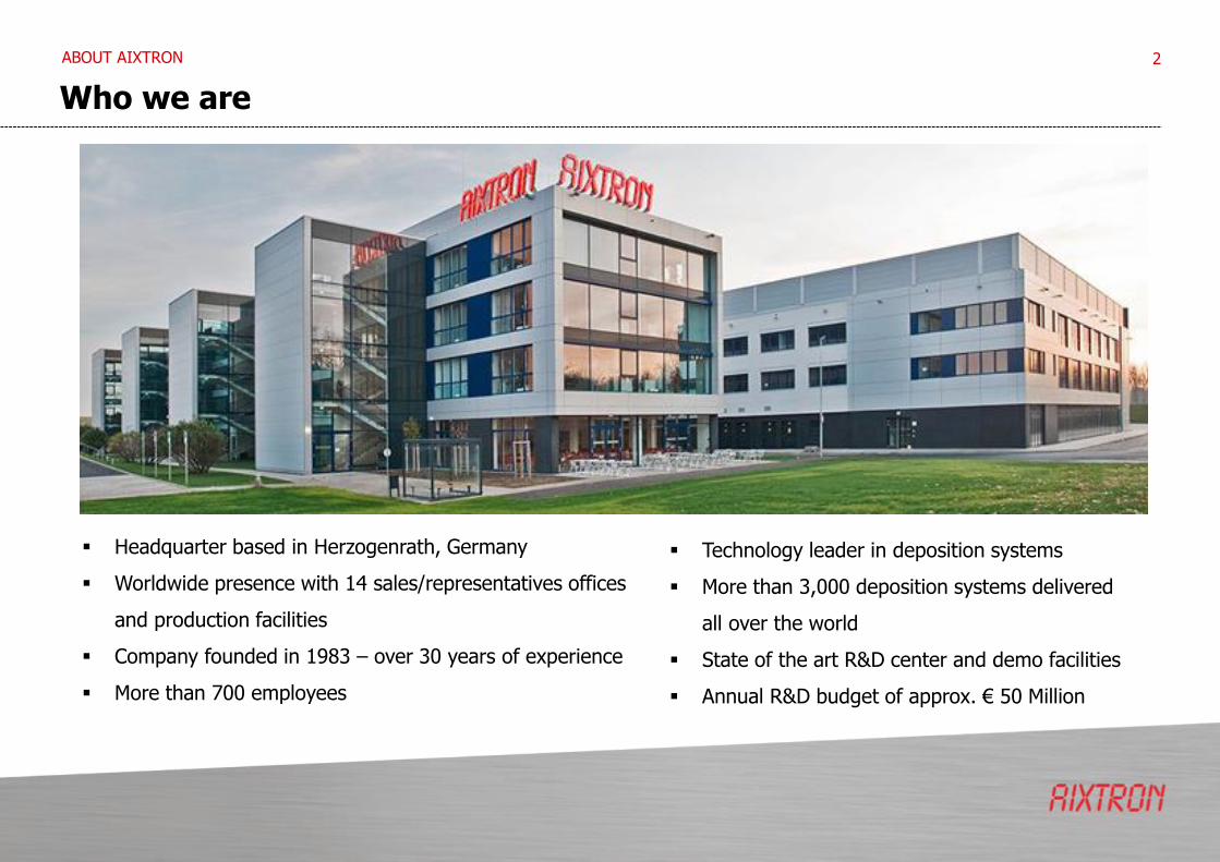
Who we are
Headquarter based in Herzogenrath, Germany
Worldwide presence with 14 sales/representatives offices
and production facilities
Company founded in 1983 – over 30 years of experience
More than 700 employees
Technology leader in deposition systems
More than 3,000 deposition systems delivered
all over the world
State of the art R&D center and demo facilities
Annual R&D budget of approx. € 50 Million
2014 | Corporate Presentation
ABOUT AIXTRON 2

AIXTRON SE Headquarters
Herzogenrath, Germany
Core of AIXTRON’s activities is
the Technology and R&D Center
near Aachen.
Focus on engineering and process
development in MOCVD and
organic semiconductors.
AIXTRON Inc.
Sunnyvale, California, USA
Focus on silicon applications for
leading suppliers of DRAM and
CMOS.
AIXTRON Ltd.
Cambridge, United Kingdom
Focus on the enhancement of
material sciences and carbon-
nanotechnology research.
3
Global Presence
ABOUT AIXTRON
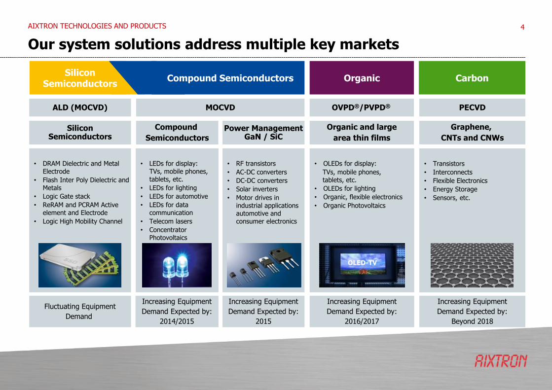
Our system solutions address multiple key markets
2014 | Corporate Presentation
SiliconSemiconductors
Compound Semiconductors
• RF transistors
• AC-DC converters
• DC-DC converters
• Solar inverters
• Motor drives inindustrial applicationsautomotive andconsumer electronics
Power ManagementGaN / SiC
MOCVD
• DRAM Dielectric and Metal Electrode
• Flash Inter Poly Dielectric and Metals
• Logic Gate stack
• ReRAM and PCRAM Active element and Electrode
• Logic High Mobility Channel
SiliconSemiconductors
ALD (MOCVD)
4
Compound
Semiconductors
• LEDs for display:TVs, mobile phones,tablets, etc.
• LEDs for lighting
• LEDs for automotive
• LEDs for datacommunication
• Telecom lasers
• ConcentratorPhotovoltaics
Fluctuating Equipment
Demand
Increasing Equipment
Demand Expected by:
2015
Increasing Equipment
Demand Expected by:
2014/2015
AIXTRON TECHNOLOGIES AND PRODUCTS
• OLEDs for display:
TVs, mobile phones,tablets, etc.
• OLEDs for lighting
• Organic, flexible electronics
• Organic Photovoltaics
• Transistors
• Interconnects
• Flexible Electronics
• Energy Storage
• Sensors, etc.
Organic and large
area thin films
Graphene,
CNTs and CNWs
Organic Carbon
OVPD®/PVPD® PECVD
Increasing Equipment
Demand Expected by:
2016/2017
Increasing Equipment
Demand Expected by:
Beyond 2018
OLED-TV

Product Features
Compound Semiconductors – MOCVD Planetary (1/2)
Planetary Technology: GaN LED, GaN HEMT, AlInGaP,Photovoltaics, Laser, SiC PE
AIX G5 HT: 56x2’’, 14x4’’, 8x6’’
AIX G5+: 5x200mm
AIX 2800G4-TM: 60x2’’, 15x4’’, 8x6’’, 5x8’’
AIX G5 WW: 10x100mm, 6x150mm
Established production platform at Tier One customers
Product Description – MOCVD
Unique Planetary reactor design Horizontal reactor type Core process know-how
Individual control of each single wafer Ideal for large wafers Best-in-class on-wafer uniformity Unique w2w adjustment capability
Lowest cost of ownership for large wafers Highest throughput 6”, 8” wafers Best-in-class precursor efficiency
"Single wafer performance with batch reactor cost benefit”
2014 | Corporate Presentation
AIXTRON TECHNOLOGIES AND PRODUCTS 5

Patented CCS Technology Vertical reactor design Core process know-how
Intrinsically uniform Wide process window
Lowest cost of ownership High throughput Low gas consumption
Compound Semiconductors – MOCVD CCS (2/2)
Close Coupled Showerhead (CCS) Technology
GaN LED
Production: Crius eXL: 75x2’’, 19x4’’
R&D: CCS 3x2’’, 6x2’’
Proven production platform at HVM customers
Product Description – MOCVD
8/3/2017
“Higher capacity and more throughput with the showerhead performance you can expect from AIXTRON”
2014 | Corporate Presentation
AIXTRON TECHNOLOGIES AND PRODUCTS
Product Features
6
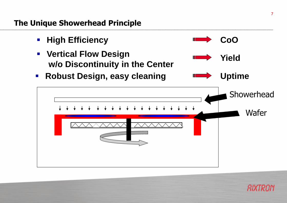
High Efficiency CoO
Vertical Flow Design
w/o Discontinuity in the CenterYield
Robust Design, easy cleaning Uptime
Showerhead
Wafer
The Unique Showerhead Principle
7
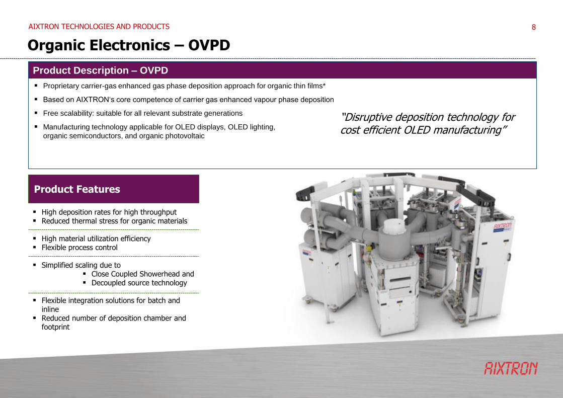
Proprietary carrier-gas enhanced gas phase deposition approach for organic thin films*
Based on AIXTRON‘s core competence of carrier gas enhanced vapour phase deposition
Free scalability: suitable for all relevant substrate generations
Manufacturing technology applicable for OLED displays, OLED lighting,
organic semiconductors, and organic photovoltaic
High deposition rates for high throughput Reduced thermal stress for organic materials
High material utilization efficiency Flexible process control
Simplified scaling due to Close Coupled Showerhead and Decoupled source technology
Flexible integration solutions for batch and inline
Reduced number of deposition chamber and footprint
Organic Electronics – OVPD
Product Description – OVPD
8/3/2017
“Disruptive deposition technology for cost efficient OLED manufacturing”
2014 | Corporate Presentation
Product Features
AIXTRON TECHNOLOGIES AND PRODUCTS 8

OLED coating technology – Perceived disadvantages of VTE
VTE
• Efficiency < 70 %Degradation of org. materials
• Uptime frequent cleaning of chamber wallsfrequent source refill (high vacuum)
• Fixed layer sequence
• Economic Deposition (> 70 %)No Degradation of organic materials
• Uptime No parasitic depositionNo interruptions for source refill
• Flexible layer sequence
OVPD
Short thermal exposure source (STExS)
9

OVPD STEx Source
00:00 00:30 01:00 01:30 02:00
0
10
20
30
40
50
60
Runs
Average
Rate
(A
/s)
time (mm:ss)
Avg. Rate: 8.8 A/sR2R: ± 0.6%
Avg. Rate: 26.3 A/sR2R: ± 0.5%
Avg. Rate: 52.3 A/sR2R: ± 0.7%
STEx Source
(Short Thermal Exposure Source)
• Constant Source temperature => three different rates subsequently
• Material is stored at room temperature in vacuum
• Material can be refilled without downtime
10
Reduced and constant thermal exposure of organic material

OVPD Unique Advantages
Efficient Material Utilization > 70 % (Gen 8 and beyond)
High Availability No frequent cleaning
Continuous Production Continuous source refill
High throughput Highest deposition rates
Overall capital efficiency Less chambers per line
Flexibility Mutiple sources/layers per OVPD
11
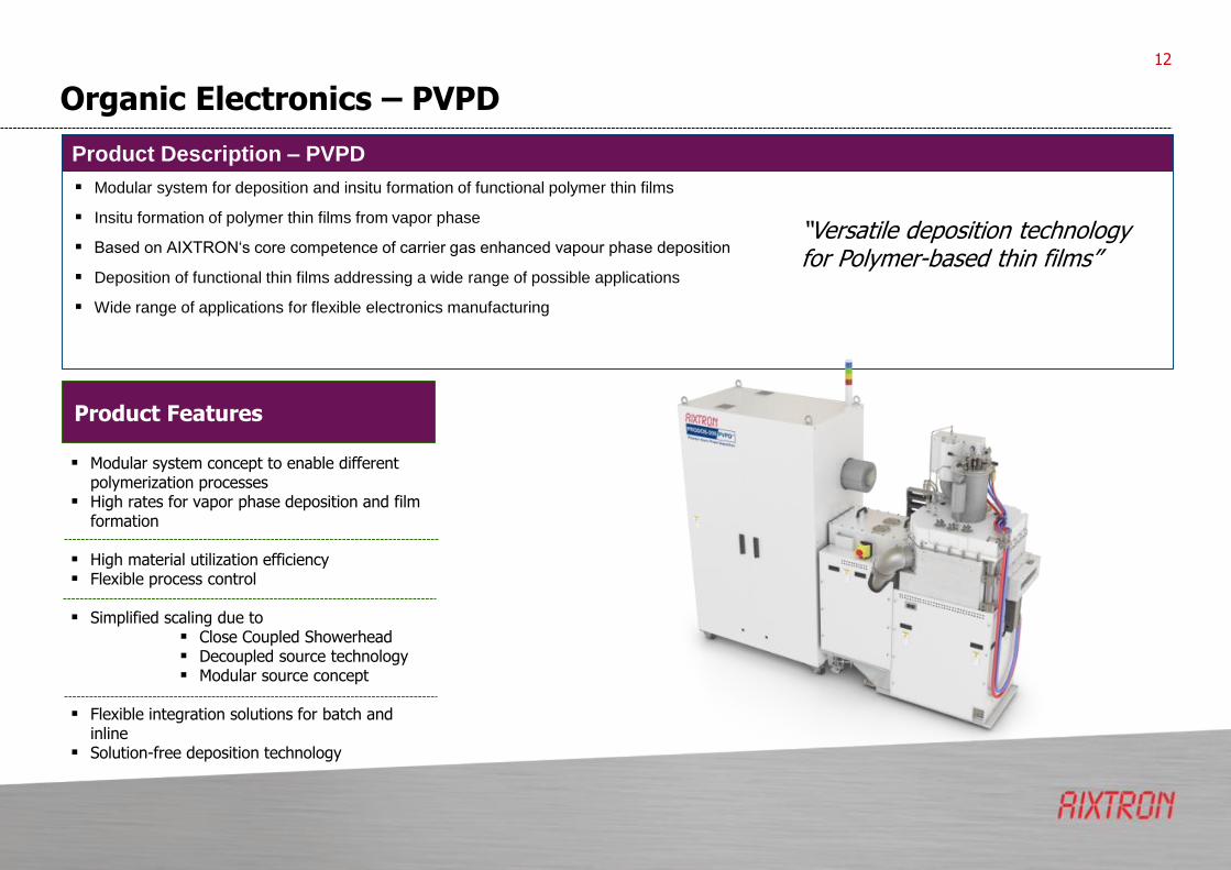
Modular system concept to enable different polymerization processes
High rates for vapor phase deposition and film formation
High material utilization efficiency Flexible process control
Simplified scaling due to Close Coupled Showerhead Decoupled source technology Modular source concept
Flexible integration solutions for batch and inline
Solution-free deposition technology
Modular system for deposition and insitu formation of functional polymer thin films
Insitu formation of polymer thin films from vapor phase
Based on AIXTRON‘s core competence of carrier gas enhanced vapour phase deposition
Deposition of functional thin films addressing a wide range of possible applications
Wide range of applications for flexible electronics manufacturing
Organic Electronics – PVPD
Product Description – PVPD
8/3/2017
“Versatile deposition technology for Polymer-based thin films”
2014 | Corporate Presentation
Product Features
12

Gen8 Demonstrator
OEC-200 Demo Cluster
Gen8/3.5 Demo Module
OLAD - Organic Large Area Demonstrator
Organic Electronics Lab at AIXTRON Headquarters
Full OLED Device Capability
• Pre-Treatment
• OLED stack Deposition by OVPD
• Full or Split Device Stack in up to 3 OVPD PM
• Optional: FMM patterning in one OVPD
• Metal Deposition by VTE
• Encapsulation – Glass Encap. in GB
• Polymer Deposition by PVPD
Single/Multi Layer Capability on large scale
Deposition on Gen3.5 (850mm x 750mm) Substrates with FMM
Deposition on Gen8 (2.2m x 2.5m) test area, Deposition performance validation via Si-Wafers andQCMs
13

AIXTRON role in EXCILIGHT
Preparation of layers and OLEDs by OVPD technique.
Characterization of deposited organic layers and OLEDs concerning lifetime and degradation.
Development of encapsulation methods for protection of OLEDs using flexible or rigid encapsulant.
14

Objectives
Improve quality and uniformity of exciplex layers using OVPD technique.
Develop encapsulation methods for protection of OLEDs using different techniques and sealants.
Improve understanding of the relevant physical and chemical processes.
Scale up the OVPD processes for future commercial OLED production.
15
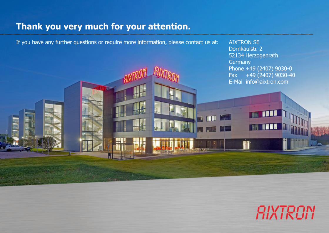
Thank you very much for your attention.
If you have any further questions or require more information, please contact us at: AIXTRON SEDornkaulstr. 252134 HerzogenrathGermanyPhone +49 (2407) 9030-0Fax +49 (2407) 9030-40E-Mai [email protected]