
Gigabit Ethernet Module Test Bed Design and...
35
Gigabit Ethernet Module Test Bed Design and Setup ECE 4006 Advisor : Dr. Martin Brooke Group 1 Harsh Sopory Kaushik Narayanan Nafeez Bin Taher
Transcript of Gigabit Ethernet Module Test Bed Design and...

Gigabit Ethernet Module
Test Bed Design and Setup
ECE 4006
Advisor : Dr. Martin Brooke
Group 1
Harsh Sopory Kaushik Narayanan Nafeez Bin Taher

Abstract
The purpose of the project is to reduce the cost of present Gigabit Ethernet
technology. It is evident that Gigabit Ethernet has the potential to be one of the most
popular and efficient communication protocols available in the market. One barrier to this
is the high cost that is currently associated with installing this technology. A Gigabit
Ethernet card for a personal computer can cost up to $600. Although all the parts on the
Ethernet card share most of this cost, a disproportionately large portion of it is associated
with the opto-electronic module that is present on the card. Most of the project efforts
will go towards trying to reduce the cost of the module. The main aim of our group for
this semester is to set up a test bed that can be used by groups in the future, to test any
modules that they have designed.
2

Introduction – What is Ethernet ?
Local Area Networks (LAN) were invented in the mid-1970s to late-1980s. LAN
technologies operate at the Data Link layer (layer 2 of the OSI Reference Model), and
Ethernet is one of a variety of different LAN types. Ethernet has been the most successful
LAN technology. It is not a singular Medium Access (MAC) layer protocol, but a family
of closely related protocols that share a common set of frame formats.
Figure 1. An early Ethernet diagram by Dr. Metcalfe
Ethernet was conceived as a passive coaxial cable medium with a contention-
based medium access protocol. Contention-based means that only one station may
transmit at a time, so a protocol is needed to fairly share access to the wire among all its
stations. Carrier Sense Multiple Access with Collision Detection (CSMA/CD) is the
protocol that enables the medium to be shared fairly among all the stations.
3

How does Ethernet work? – CSMA/CD
In CSMA/CD, each station continually monitors the wire to keep track of whether
or not any other station is transmitting. If another station is already transmitting when this
station has a frame it wants to transmit, it must defer transmission until the other station
is finished. This is the “carrier sense” portion of the technique. For diagnostic purposes,
Ethernet devices may keep a counter of such “deferrals” or times when a frame was
queued for transmission but the wire was already in use. Large number of deferrals may
indicate that the Ethernet is becoming too busy, in which case network managers can
respond by breaking up the LAN into smaller pieces using bridges.
When the medium is not being used, any station may attempt to transmit. Each
station must not only monitor the wire to ensure it is free before a frame is transmitted,
but also see that its transmission is not garbled by a “collision” with a frame from another
station. Once a collision has been detected, a station should cease transmission
immediately. In a shared medium in which only one machine can talk at a time, collisions
are an expected and unavoidable event that must be dealt with fairly.
Gigabit Ethernet
Since its inception at Xerox Corporation in the early 1970s, Ethernet has been the
dominant networking protocol. Of all current networking protocols, Ethernet has, by far,
the highest number of installed ports and provides the greatest cost performance relative
to Token Ring, Fiber Distributed Data Interface (FDDI), and ATM for desktop
connectivity. Fast Ethernet, which increased Ethernet speed from 10 to 100 megabits per
4

second (Mbps), provided a simple, cost-effective option for backbone and server
connectivity.
Gigabit Ethernet builds on top of the Ethernet protocol, but increases speed
tenfold over Fast Ethernet to 1000 Mbps, or 1 gigabit per second (Gbps). This protocol,
which was standardized in June 1998, promises to be a dominant player in high-speed
local area network backbones and server connectivity. Since Gigabit Ethernet
significantly leverages on Ethernet, existing knowledge can be used to manage and
maintain gigabit networks.
Like its predecessors, Ethernet (IEEE 802.3 10-Mbps specifications) and Fast
Ethernet (IEEE 802.3 100-Mbps specifications), Gigabit Ethernet operates at the Data
Link layer (layer 2 of the OSI Reference Model) while allowing for reliable
communications between applications of the Network Layer (layer 3) and the Transport
layer (layer 4). It also operates in the Physical Layer (layer 1) acting as an interface
between the Media Access Control (MAC) layer and the transceivers in Gigabit Ethernet
hardware.
Physical Specifications of Gigabit Ethernet
The work on Gigabit Ethernet at the physical layer has been split between two
projects within the IEEE 802.3 committee. The initial project known as 802.3z has
produced the 1000BASE-X family of standards. This project has defined three physical
layers: 1000BASE-CX (short-haul copper), 1000BASE-LX (long-wavelength optics),
and 1000BASE-SX (short-wavelength optics).
5
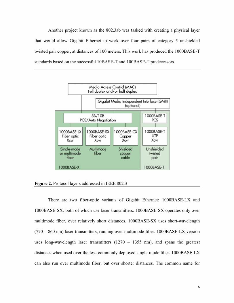
Another project known as the 802.3ab was tasked with creating a physical layer
that would allow Gigabit Ethernet to work over four pairs of category 5 unshielded
twisted pair copper, at distances of 100 meters. This work has produced the 1000BASE-T
standards based on the successful 10BASE-T and 100BASE-T predecessors.
Figure 2. Protocol layers addressed in IEEE 802.3
There are two fiber-optic variants of Gigabit Ethernet: 1000BASE-LX and
1000BASE-SX, both of which use laser transmitters. 1000BASE-SX operates only over
multimode fiber, over relatively short distances. 1000BASE-SX uses short-wavelength
(770 – 860 nm) laser transmitters, running over multimode fiber. 1000BASE-LX version
uses long-wavelength laser transmitters (1270 – 1355 nm), and spans the greatest
distances when used over the less-commonly deployed single-mode fiber. 1000BASE-LX
can also run over multimode fiber, but over shorter distances. The common name for
6

short-wavelength lasers is “850 nm”, and the common name for long-wavelength lasers is
“1300 nm”. Both of those wavelengths identify the point of minimum optical attenuation
within the range of wavelengths specified above.
1000BASE-X supports both 50/125 nm and 62.5/125 nm multimode fiber, as well
as 10 nm single-mode fiber. Table I below shows the maximum distance (assuming full
duplex operation) that is supported by 1000BASE-LX and 1000BASE-SX. These
distances depend on the type of fiber, as well as which wavelength is used.
Table I. Gigabit Ethernet over Fiber
Fiber Dimensions 1000BASE-SX
(770 – 860 nm) 1000BASE-LX (1270 – 1355 nm)
Multimode…50/125 nm 525 m 550 m Multimode…62.5/125 nm 260 m 550 m Single Mode…10/125 nm N/A 3000 m
The 1000BASE-X family of standards includes one copper-based variant,
1000BASE-CX. 1000BASE-CX operates over two pairs of 150 � shielded twisted pair
cable, terminating in two possible electrical pair connectors. This physical layer was
designed for server-to-switch interconnection in relatively small rooms, which is why the
distance is limited to 25 meters. Table II below, compares 1000BASE-CX to 1000BASE-
T, which is intended to be used for desktop interconnection at 1000 Mbps.
Table II. Comparison of Nonfiber-Optic Gigabit Ethernet Media
Medium Length Medium Type 1000BASE-CX 25 m 150 � (STP) 1000BASE-T 100 m 100 � (UTP)
7

1000BASE-T has been developed with a goal of 1000 Mbps operation over a 100
meter category 5 unshielded twisted pair infrastructure. 1000BASE-T is related to the
100BASE-T2 standard, which allowed 100 Mbps operation over two pairs of category 3
wiring. 1000BASE-T will use all four pairs of the RJ-45 connector and squeeze five
times the bandwidth out of each pair, compared to 100BASE-T2. The key is that for 1000
Mbps operation to be practical, it must be full duplex, which is just one of the many
challenges involved in operating at such a high speed over twisted pair wiring, even
category 5 wiring.
Benefits of Gigabit Ethernet
One of the main benefits of Gigabit Ethernet is the great increase in data rates that
it offers compared to its predecessors. It offers a 100 fold increase over the original
version of Ethernet and a 10 fold increase over Fast Ethernet. Another benefit is that
Gigabit Ethernet is based on the already widespread Ethernet LAN protocol. This means
that the additional cost involved in implementing Gigabit Ethernet is not as high as the
cost of implementing a brand new protocol. There are savings in terms of hardware costs,
but there are also significant savings that extend to the training of system and support
personnel on this technology. This is because those personnel familiar with Ethernet
would find Gigabit Ethernet to be very similar in structure and methodology. The spread
of this technology would also make it possible for other services to be offered, such as
video based services, which require the technology to be capable of supporting high data
rates. Examples of these video applications are video conferencing and complex imaging.
Also in the future, it might be possible to bring in digital television content on the same
8
link. In general, it can be said that Gigabit Ethernet offers great flexibility and potential in
terms of the services it can support. This is an important reason why this technology
should be made as cheap as possible so that the consumers at large can take advantage of
it.
Immediate Goals
The immediate goal of our research group for this semester was to set up a test
bed that could be used to test future modules that are designed. The steps decided upon to
achieve this are given as follows:
1) Purchase a Gigabit Ethernet Card with an opto-electronic module on it.
2) Detach the module from the card and set up an evaluation board for the module.
3) Test the module on the evaluation board to make sure that the board is capable of
transmitting data at gigabit rates.
4) Once the board and the module have been tested successfully, the evaluation
board with the module on it is to be connected back to the original Ethernet card.
5) This setup is then to be tested with another Gigabit Ethernet card, so as to see
whether data is transmitted with the same level of reliability of efficiency as there
would be if two Gigabit Ethernet cards were connected directly.
This setup can be used as a test bed for future research into the design of the opto-
electronic modules because if it is determined that this setup works, then, theoretically,
when the module present on the evaluation board is replaced by a module that is designed
by the research team, it can be expected that if the module is designed correctly, the
system should work. If it does not work, then it will probably be reasonable to assume
9
that there is a flaw in the design of the module, because it will be known that the board
and it connection to the card work with another module.
Brief Description of Module
The module that was used in this project was the Agilent HFBR 53D5. This
basically consists of a transmitter section and a receiver section. The transmitter section
consists of an 850 nm Vertical Cavity Surface Emitting Laser (VCSEL) in an Optical Sub
Assembly (OSA). This is driven by an IC that converts differential signals into a signal
capable of driving the laser. The receiver consists of a silicon PIN diode that is mounted
on the OSA with a transimpedance preamplifier IC. The OSA is connected to a bipolar
circuit that provides post amplification and quantization of the signal. A signal detect
circuit is also present in the post-amplification part of the circuit, and is used to indicate
when the input is valid data and when it is not.
Design Steps and Considerations
The first step in our project was to set up an evaluation board to test the HFBR
53D5 to ensure that it could transmit data at Gigabit rates. Agilent provides an evaluation
board for the testing of this module and the schematic of what the Agilent board would
look like with all the parts and the module on it is given in Figure 3.
10

Figure 3. Schematic of Agilent Evaluation Board for HFBR 53D5 module.
We decided that for testing purposes, it would be cheaper to use an evaluation
board manufactured here at Georgia Tech itself. To this end, the board specifications
were obtained from the Agilent website and the board shown in Figure 4 was made.
11

Figure 4. Georgia Tech Evaluation Board.
After going over the circuit layout of the Agilent evaluation board, it was decided that all
the parts would not be required. The circuit layout that was used is given in Figure 5.
12

Figure 5. Circuit Layout to be used on Georgia Tech Evaluation Board.
In the construction of this board, there were certain factors that had to be kept in
mind. The first one was regarding the power supply filtering circuit and its location, and
associated concerns such as the accompanying ground and supply planes used for this
power supply. The second one was regarding the transmission lines and their
terminations on the board.
Regarding the first concern about the power supply filtering circuit, the problem
was dealt with by removing the need for the circuit. The circuit was required on the
Agilent board because just one power source was supposed to be supplying power to both
13

the transmitter and the receiver in the transceiver. The reason for this setup was to save
space when this transceiver was actually being used. By having just one power supply for
both the parts, space would be saved on the Gigabit Ethernet card where this transceiver
was actually going to be used. By having the same power supply though, an additional
consideration was introduced, namely that the power supply of one part would now be
sensitive to any changes that might be caused in the power supply due to the operation of
the other part of the transceiver. To account for this the power supply filtering circuit was
required. By having this, it would be possible to keep the two parts of the transceiver
quite isolated and independent of each other’s power supply considerations.
This problem was dealt with on our board by using two separate +5V power
supplies for the receiver and the transmitter stages in the module. This eliminated the
need to construct a power supply filtering circuit on the board. Also, it did not seem that
the absence of this circuit would cause any problems in the future when the evaluation
board with the transceiver was to be tested with another Gigabit Ethernet card.
The second concern was regarding transmission lines and their terminations on
the evaluation board. This problem was solved by eliminating transmission lines from the
board. This was possible because since the module was to carry data at a Gigabit per
second, the maximum frequency of the signal would be 500 Mhz. If the maximum
frequency were 500 Mhz, in order to avoid the wires looking like transmission lines, their
length would have to be less than 1/4th the wavelength of the signal. Just to be on the safe
side, care was taken to keep the length of the lines to 1/10th of this signal wavelength,
which found to be 6 cm. It can be seen from the board given in Figure 4 that all of the
14

trace lengths are less than 6 cm. Also by avoiding any sharp angles on the board, the
chance of the wires behaving like transmission lines towards the signal was decreased.
In addition to these considerations, further thought was also given to reducing the
susceptibility of the signals to noise. This problem was solved to a large extent, by using
differential inputs and outputs for this board. Differential inputs are more useful than
single ended inputs because differential inputs carry two signals that are the inverse of
each other. On taking the difference of the signals, if a positive value is obtained it means
the signal can be used; a negative value means it cannot be used. The common mode
noise that is usually associated with these circuits ends up being cancelled out of the
circuit because the difference of the two signals is taken. This can be seen quite clearly
using a simple equation: (A + Noise) - (-A + Noise) = 2A
Hence, the noise is cancelled, leaving just the original signal. The usage of single
ended inputs, as has been done in the past, results in the system being more susceptible to
any noise that might be introduced on the channel.
The rest of the parts that were to be placed on the evaluation boards consisted
mainly of resistors and capacitors. These parts fulfill various purposes. The 0.01 �F
capacitors that were to be used were mainly used as decoupling capacitors. Decoupling
capacitors play an extremely important role in high-speed circuits such as this. The
reason for this is that they are used to make sure that the power supply is kept separate
(i.e. decoupled) from the circuit. This is important because of the presence of various
inductances that are inbuilt into the circuit. On our evaluation board, these inductances
are associated with the power supply wire, the evaluation board itself and the solder bond
used for the transceiver pins and the elements on the board. The presence of these
15

inductances means that if any high-speed transients are generated during the switching of
the circuit, they will be stopped by the inductances. The decoupling capacitors are then
used to handle this excess charge that is present in the circuit. By preventing this excess
charge from reaching the circuit, the power supply to the circuit can be maintained within
the recommended limits and the circuit will be protected from damage. It can be seen
from the circuit layout that the capacitors are present only on the power supply lines.
These factors are extremely important when considering circuits where the minimization
of noise is important. Another way in which the function of these capacitors is made
evident is by the fact that they are placed as close to the pins of the circuit as possible.
This is to ensure that the inductance between the capacitor and the pin, due to the wire, is
as low as possible. Further information about the need for these capacitors and the effect
their absence can have on the circuit is included in Appendix A.
The resistors to be used were to fulfill two main purposes; firstly to terminate
transmission lines and secondly, to bias the amplifiers. The network of 68� and 191�
resistors that can be seen in Figure 5 have been placed on the lines leading to the
transmitter. They are used to terminate the transmission lines that are present on the
Gigabit Ethernet card and run from the card to the evaluation board. Also, the resistors
are used to bias the amplifiers present in the transmitter and in the receiver.
Regarding the choice of connectors to be used on the board, SMA connectors
were chosen as opposed to BNC connectors. This was firstly because they can conduct
signals up to 18 GHz, which is much higher than BNC connectors. Secondly, and more
importantly, they are smaller than BNC connectors, and so make it much easier for other
components to be placed on the board.
16

A final consideration in the board design that was kept in mind was that all
connections to the ground plane should be as close to each other as possible, if not almost
at the same point. This avoided the problem of ground inductances that can come up if
the parts are not grounded properly. This problem comes up because at certain
frequencies, even the ground begins to exhibit some inductance. Hence by grounding the
circuit elements at different point, ground inductances come into effect between the
different points and this can cause problems when excess charge is being conducted to
ground.
After receiving the board, it was noticed that the top and the bottom sides of the
board were unconnected. If left uncorrected, this flaw would result in the signals not
getting through from the transceiver to the rest of the circuit. In order to account for this,
4 small pieces of wire were pushed through holes that had been drilled on the board for
this purpose, and were soldered on both sides, forming the connections. Also, in order to
make sure that the power would get through from the power supply connectors, solder
was allowed to drip through along the power supply connector pins, forming a connection
from one side of the board to the other.
Once the evaluation board had been setup completely with the module on it, it
was to be tested for its handling of data at Gigabit rates. If it passed this test, it would
then be connected to the original Gigabit Ethernet card that the module was on. This was
to be done by soldering RG174 50 � coaxial cables to the pin positions on the Gigabit
card, and by connecting SMA connectors at the other end of the cable to the connectors
on the board. A part of the metal shielding of the receiver cables was to be soldered
together, as was a part of the metal shielding of the transmitter cables. This was done to
17

tie the transmission lines to a common ground. In addition to connecting these pins, the
signal detect pin was also connected to the card, using a piece of wire. For the pins that
corresponded to the traces that run to the transmitter, the termination network present on
the evaluation board would terminate the RG 174 cable. On the Gigabit card though,
there was another similar network that was also meant to terminate the transmission lines
till that point. This network had to be taken off the card to prevent the transmitted signals
from seeing two impedances before leaving the card. Similarly, on the receiver lines, the
resistor network on the gigabit card also had to be removed. A circuit diagram of the
whole setup is given in Figure 6, with the boxed elements representing the elements that
needed to be removed.
Figure 6. Diagram of whole setup and of the elements to be removed.
Once the evaluation board and the card were connected, a diagnostic test was to
be run on the card to determine whether it was carrying the data or not. A fiber optic link
would then be set up between the transceiver on the board and another Gigabit Ethernet
18

card. This link was to be tested using a diagnostic program that was provided along with
the Gigabit card software. The passing of this test would imply the successful conclusion
of our project.
A final consideration that had initially been overlooked was the connection of the
ground pin from the evaluation board to the ground pin on the gigabit card. The initial
absence of this connection prevented the setup from working the first time the card was
plugged into the computer. Once the connection was made, using wire wrap, the setup
was found to work well.
Problems Faced
The main problems faced until during this project, mainly concerned the soldering
of the components onto the evaluation board. One of the reasons for this was the
unfamiliarity with soldering, of the group members prior, to this project. The other reason
for this was the size of the components that had to be soldered onto the board. Due to
their being very small, soldering was made quite difficult. Problems also occurred
because of the manner in which the board had been constructed, with the top and bottom
halves unconnected. The testing of the evaluation boards with the modules had to be
delayed initially because the vias had not been inserted through the boards to form the
connections, and the power supply pins were not connected to both sides of the board.
Hence it was found that when the power connectors were soldered onto the bottom half
of the board, no power was getting through to the other side. To rectify this situation,
solder was allowed to drip through from one side of the board to the other, forming a
connection between the two sides of the board, that allowed the power to flow correctly.
19

After the initial tests, when the RG 174 cable had to be soldered onto the card,
some problems were encountered. One of these problems was due to the thinness of the
cable. To make the connection between the cable and the points on the card, the cable
shielding had to be stripped away to reveal the metal. This was a little challenging
because it was very easy to cut the cable completely, as compared to removing just the
shield. During the soldering of the wires, care also had to be taken that they were not bent
very sharply so as to create a problem with the signals being transmitted through them.
For this reason, they were placed flat on the card and small lengths of the unshielded
portion of the cable were soldered to the pin points. It had been thought prior to soldering
that a hot glue gun would be used to ensure that that wires did not move. The usage of hot
glue though would have meant great problems if the need arose to remove the wires from
the board. Hence, electrical tape was used to temporarily hold the wires in place.
Soldering was also made more difficult because of the limited length of wire that
could be left unshielded. The RG174 cable that was being was expected to have to carry
upto the fifth harmonic of the primary 500 MHz signal. This would mean that the highest
frequency component of the signal would be 2.5 Ghz. On calculating the wavelength at
this frequency, and keeping in mind that the length of the unexposed cable should not be
more that 1/10th of the wavelength, the length of unexposed cable that could be used was
1.2 cm.
Another problem arose when trying to remove all the resistive networks from the
card. Since they were very small, it proved to be a problem trying to remove them by
heating the solder around them and then pulling them up. High soldering temperatures
were not used for fear of damaging the board. Also it was found that the parts were also
20

being held in place by traces of strong glue. Finally, pliers were used to pry the
components off the card, without damaging it.
Results
Once the evaluation board had been constructed keeping in mind the design
considerations, and the modules and parts soldered onto it, the whole setup was tested to
see if the board and the transceiver could carry data at a Gigabit rate. A diagram of the
test setup is given in Figure 7.
X
Ch2 Oscilloscope
Pattern Generator
Ch1 Oscilloscope
Power
eFigure 7. Layout of test setup.
Initially, the transmitter connectors were connected to
(Tektronix CSA 8000) and receiver connectors to the digital
694C). A picture of the equipment used can be found in A
connected to a digital oscilloscope so that an eye diagram c
the board and the module were required to handle a data rate
Pattern Generator
Fiber Optic Cabl
TXR
TXRX
the signal pattern generator
oscilloscope (Tektronix TDS
ppendix B. The board was
ould be obtained. Although
of a gigabit per second, the
21

testing was started off with a data rate of 1.4 gigabit per second, using the PN 7 encoding
scheme. The eye diagram obtained is shown in Figure 8.
Figure 8. Eye diagram for 10 m cable at 1.4 Gigabit/s with PN 7 encoded data.
The eye diagram is a very common parameter by which signal quality, and hence
the working of the circuit, can be determined. The ‘eye’ is formed by the superimposition
of pseudo random bit patterns. If the signals do not transition at exactly the same time
every time, the resulting eye appears to be narrower than an eye formed when signals
transition at the same time every time. This signal variance is referred to as jitter and it
can cause Inter Symbol Interference, which results in bits errors. ISI occurs because a
particular bit influences the interpretation of the subsequent bit, thereby leading to the bit
22

being wrongly assigned. The height of the eye is governed by the distortion that is caused
due to noise that occurs when the patterns are sampled. The thicker the lines, the more the
noise, and the smaller the eye will be.
Typically, the way in which the suitability of an eye is determined is by the use of
an eye mask. An eye mask corresponds to the minimum dimensions that the eye is
supposed to have if the system is working properly. This can be crudely determined by
superimposing the specified eye mask into the eye in the eye diagram, provided they have
the same units on the axes. In this case, this eye mask in Figure 9 corresponds to the eye
expected when the HFBR 53D5 optical transceiver is used.
Figure 9. Eye Mask.
On superimposing the eye mask on to the eye diagram that had been obtained, it
was found that the eye mask fit in, indicating that the eye was acceptable. This in turn
meant that the module and the board were probably working properly and were
acceptable for gigabit rate data transmission. Channel 1 in the eye diagram represented
one receiver channel and channel 2 represented the other. It can be seen from the eye
23

diagrams that the signal on channel 1 was a little worse (more noise) than the signal on
channel 2 and that each signal was the inverse of the other. The inverse signals were
expected since the differential receiver signals were being looked at. On looking at the
parts on the board, it was decided that some of the solder joints on the board might not
have been formed properly. This was looked into but no solder joint was found to be
defective.
As a rough measure of signal quality, the eye diagram is quite useful. However,
when trying to determine the suitability of a data link, it is always advisable to run Bit
Error Rate tests, using a Bit Error Rate tester on the system. This should be done so as to
get the actual number of errors that occur because such errors would not necessarily be
evident from an eye diagram. To this end, the receiver channel 1 was connected to a bit
error rate tester to find out how many errors were occurring per gigabit of transmitted
data, using the PN 7 encoding scheme and a data rate of 1.4 Gbps. It was found that no
errors occurred for a time duration of a minute and a half, which was proof that the board
was transmitting the data correctly.
The initial test was carried out using a 10 m long fiber optic cable. This cable was
then replaced with a 100 m long cable. The point of using the longer cable was to check
the affect of attenuation on the signal and to see if the error rate would increase
drastically due to it. The eye diagram that was obtained with a data rate of 1.4 Gigabit/s is
shown in Figure 10.
24

Figure 10. Eye diagram for 100 m cable at 1.4 Gigabit/s with PN 7 encoded data.
It can be seen from the eye diagram that apart from one receiver channel
displaying more noise than the other, the quality of the signals was about the same as
when the 10 m cable was used. This fact was again proven by using the bit error rate
tester, which again showed that there were no errors for a minute and a half.
The data encoding that had been used till this point was the PN 7 scheme, in
which at most seven 1’s or 0’s are sent consecutively. The data transmission was found to
be quite good while using this scheme. With the 100 m cable though, a PN 23 scheme
was also used. This is a more complex and rigorous scheme because it sends up to
twenty-three 1’s or 0’s in a row. Hence, at the end of a 1 or 0 sequence, the chances of
25

the first 1 or 0 of the next sequence being detected are lower. As a result, at 1.4 Gigabit/s,
the number of errors was extremely high and so the data rate had to be reduced. On
reducing the data rate to 1.2 Gigabit/s, an error rate of 2.3 errors per Megabit (106) was
obtained. Although this is not a very good error rate, it did show that the board and
module could still handle a more complex encoding scheme as well.
The final aim of the project for this semester was to connect the evaluation board
with the transceiver to the gigabit Ethernet card, and to test a link between this setup and
another gigabit Ethernet card. The card connected to the evaluation board is shown in
Figure 11.
Figure 11. Picture of the Evaluation board (on right) connected to Gigabit Card.
26

The gigabit card was then plugged into a computer and a single fiber optic cable
was run from the receiver to the transmitter. A picture of this setup can be seen in
Appendix B. A diagnostic test was then run on the card. The diagnostic package had been
included with the card when it was purchased. The first time this test was tried, it failed
because the ground pin of the signal detect had not been connected to the ground pin on
the Gigabit card. After making the connection though, the test passed. The card was then
connected to a card in another computer, using two fiber optic cables that had a length of
100m. The cable from the transmitter of one module was connected to the receiver of the
other module and cable from the receiver of one was connected to the transmitter of the
other. Another diagnostic test was then run, in which one of the computers was
configured as a sender and another as a receiver. In this test, test packets were sent from
the sender to the receiver and the program kept track of how many packets were
transmitted successfully and how many errors came up. A screen capture of this count is
given in Figure 12.
27

Figure 12. Screen capture of transmitted and received packets.
It can be seen from the Figure that there were no failures in the transmission and
the sending of the packets. The same test was then run with the sender and responder
functions switched between the computers. This too did not result in any failures. This
test was used to prove that the link was functioning properly. In addition to this test, an
additional test was carried out to test the Ethernet link. A file was transferred from one
computer to the other. This file was then transferred back from the second computer to
the first. A screen capture of the two computers being shown on the same desktop is
given in Appendix B. This test further confirmed that the link between the computers was
working properly.
28

Bibliography
[1] Stallings, Williams, Data & Computer Communications: Sixth Edition
[2] Technology Brief: Introduction to Gigabit Ethernet, Available HTTP: http://www.cisco.com/warp/public/cc/techno/media/lan/gig/tech/gigbt_tc.htm
[3] Ethernet, Available HTTP:
http://www.yale.edu/pclt/COMM/ETHER.HTM
[4] Gigabit Ethernet by Cisco Systems, Available HTTP:
http://rasi.lr.ttu.ee/~araja/sidealused/GIGA~1.HTM
[5] Intel Networking Technologies: Gigabit Ethernet, Available HTTP:
http://www.intel.com/network/connectivity/resources/technologies/gigabit_ethernet.htm
29

Appendix A
To gain a better understanding of the effect of the capacitances on the circuit, a
SPICE simulation was done. The circuit that was used was not intended to be an accurate
replica of the board that was built, but it modeled the inductors and the capacitors that
were encountered in the circuit. It was found that a 0.01 uF capacitor would block
frequencies between 10 – 100 Mhz and a 0.1 uF capacitor would block frequencies
between 1-10 Hz. The whole circuit that was simulated is given in Figure A1.
Figure A1. Modeling effect of inductance and capacitance on circuit.
It was found that when the 0.01 uF cap was removed, the power supply voltage at
Va displayed oscillations as shown in Figure A2.
30
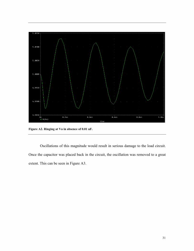
Figure A2. Ringing at Va in absence of 0.01 uF.
Oscillations of this magnitude would result in serious damage to the load circuit.
Once the capacitor was placed back in the circuit, the oscillation was removed to a great
extent. This can be seen in Figure A3.
31

Figure A3. Greatly reduced oscillation at power supply.
It can be seen from the Figures A2 and A3 that the oscillation in A2 had a much
greater value than in A3 meaning that the 0.01 uF capacitor had a damping effect on the
oscillation.
Since the 0.01 uF capacitor was the only capacitor that was used on the board, its
need can quite clearly be seen from this simulation.
32

Appendix B
Figure B1. Digital Oscilloscope, Pattern Generator and Bit Error Rate Tester.
33

Figure B2. Setup of the Gigabit Card connected to computer and to Evaluation Board.
34

Figure B3. Confirmation of Ethernet Link – Both computers on LAN.
35