Giant Magnetic Band Gap in the Rashba-Split Surface State ... · SCIENTIFIC REPORTS 7 ã 3353...
8
1 SCIENTIFIC REPORTS | 7: 3353 | DOI:10.1038/s41598-017-03507-0 www.nature.com/scientificreports Giant Magnetic Band Gap in the Rashba-Split Surface State of Vanadium-Doped BiTeI: A Combined Photoemission and Ab Initio Study I. I. Klimovskikh 1 , A. M. Shikin 1 , M. M. Otrokov 1,2,3 , A. Ernst 8,10 , I. P. Rusinov 1,2 , O. E. Tereshchenko 1,5,6 , V. A. Golyashov 1,5 , J. Sánchez-Barriga 9 , A. Yu. Varykhalov 9 , O. Rader 9 , K. A. Kokh 1,6,7 & E. V. Chulkov 1,2,3,4 One of the most promising platforms for spintronics and topological quantum computation is the two- dimensional electron gas (2DEG) with strong spin-orbit interaction and out-of-plane ferromagnetism. In proximity to an s-wave superconductor, such 2DEG may be driven into a topologically non-trivial superconducting phase, predicted to support zero-energy Majorana fermion modes. Using angle- resolved photoemission spectroscopy and ab initio calculations, we study the 2DEG at the surface of the vanadium-doped polar semiconductor with a giant Rashba-type splitting, BiTeI. We show that the vanadium-induced magnetization in the 2DEG breaks time-reversal symmetry, lifting Kramers degeneracy of the Rashba-split surface state at the Brillouin zone center via formation of a huge gap of about 90 meV. As a result, the constant energy contour inside the gap consists of only one circle with spin-momentum locking. These findings reveal a great potential of the magnetically-doped semiconductors with a giant Rashba-type splitting for realization of novel states of matter. Two-dimensional electron systems have been attracting the researchers interest for many years due to a number of unique electronic effects. A classical example is the quantum Hall effect 1 – a phenomenon of simultaneous transverse resistance quantization and longitudinal resistance drop, arising in a high-mobility two-dimensional electron gas (2DEG) under a strong magnetic field. Aſter this discovery it was realized that a similar behavior can be achieved without an external field in materials with a strong spin-orbit interaction (SOI), and the quantum spin 2 and anomalous 3 Hall effects were predicted to occur in the 2D paramagnetic and ferromagnetic (FM) insu- lating systems, respectively. ese and other intriguing findings 4–7 have established a field where the spin-orbit and magnetic effects interplay is aimed at promising applications in spintronics and quantum computing 4, 8–12 . Of particular interest is the SOI effect on the 2DEG systems with broken inversion symmetry, manifesting itself in the so-called Rashba splitting of the electronic states 13 . It has been predicted that, being proximitized to a magnetic insulator on the one hand and to an s-wave superconductor on the other, a semiconductor thin film with a Rashba splitting may undergo a peculiar phase transition and turn into a topological superconductor 6 . According to the proposal, a proximity of magnetic insulator to the semiconductor breaks the time-reversal 1 Saint Petersburg State University, 198504, Saint Petersburg, Russia. 2 Tomsk State University, 634050, Tomsk, Russia. 3 Donostia International Physics Center (DIPC), 20018 San Sebastián/Donostia, Basque Country, Spain. 4 Departamento de Física de Materiales UPV/EHU, Centro de Física de Materiales CFM - MPC and Centro Mixto CSIC-UPV/EHU, 20080 San Sebastián/Donostia, Basque Country, Spain. 5 A.V. Rzhanov Institute of Semiconductor Physics, 630090, Novosibirsk, Russia. 6 Novosibirsk State University, 630090, Novosibirsk, Russia. 7 V.S. Sobolev Institute of Geology and Mineralogy, 630090, Novosibirsk, Russia. 8 Max Planck Institute of Microstructure Physics, Weinberg 2, 06120, Halle, Germany. 9 Helmholtz-Zentrum Berlin für Materialien und Energie, Elektronenspeicherring BESSY II, Albert-Einstein-Strasse 15, 12489, Berlin, Germany. 10 Institut für Theoretische Physik, Johannes Kepler Universität, A 4040, Linz, Austria. Correspondence and requests for materials should be addressed to I.I.K. (email: [email protected]) Received: 7 February 2017 Accepted: 28 April 2017 Published: xx xx xxxx OPEN
Transcript of Giant Magnetic Band Gap in the Rashba-Split Surface State ... · SCIENTIFIC REPORTS 7 ã 3353...

1Scientific RepoRts | 7: 3353 | DOI:10.1038/s41598-017-03507-0
www.nature.com/scientificreports
Giant Magnetic Band Gap in the Rashba-Split Surface State of Vanadium-Doped BiTeI: A Combined Photoemission and Ab Initio StudyI. I. Klimovskikh 1, A. M. Shikin1, M. M. Otrokov1,2,3, A. Ernst8,10, I. P. Rusinov1,2, O. E. Tereshchenko1,5,6, V. A. Golyashov1,5, J. Sánchez-Barriga 9, A. Yu. Varykhalov9, O. Rader9, K. A. Kokh1,6,7 & E. V. Chulkov1,2,3,4
One of the most promising platforms for spintronics and topological quantum computation is the two-dimensional electron gas (2DEG) with strong spin-orbit interaction and out-of-plane ferromagnetism. In proximity to an s-wave superconductor, such 2DEG may be driven into a topologically non-trivial superconducting phase, predicted to support zero-energy Majorana fermion modes. Using angle-resolved photoemission spectroscopy and ab initio calculations, we study the 2DEG at the surface of the vanadium-doped polar semiconductor with a giant Rashba-type splitting, BiTeI. We show that the vanadium-induced magnetization in the 2DEG breaks time-reversal symmetry, lifting Kramers degeneracy of the Rashba-split surface state at the Brillouin zone center via formation of a huge gap of about 90 meV. As a result, the constant energy contour inside the gap consists of only one circle with spin-momentum locking. These findings reveal a great potential of the magnetically-doped semiconductors with a giant Rashba-type splitting for realization of novel states of matter.
Two-dimensional electron systems have been attracting the researchers interest for many years due to a number of unique electronic effects. A classical example is the quantum Hall effect1 – a phenomenon of simultaneous transverse resistance quantization and longitudinal resistance drop, arising in a high-mobility two-dimensional electron gas (2DEG) under a strong magnetic field. After this discovery it was realized that a similar behavior can be achieved without an external field in materials with a strong spin-orbit interaction (SOI), and the quantum spin2 and anomalous3 Hall effects were predicted to occur in the 2D paramagnetic and ferromagnetic (FM) insu-lating systems, respectively. These and other intriguing findings4–7 have established a field where the spin-orbit and magnetic effects interplay is aimed at promising applications in spintronics and quantum computing4, 8–12.
Of particular interest is the SOI effect on the 2DEG systems with broken inversion symmetry, manifesting itself in the so-called Rashba splitting of the electronic states13. It has been predicted that, being proximitized to a magnetic insulator on the one hand and to an s-wave superconductor on the other, a semiconductor thin film with a Rashba splitting may undergo a peculiar phase transition and turn into a topological superconductor6. According to the proposal, a proximity of magnetic insulator to the semiconductor breaks the time-reversal
1Saint Petersburg State University, 198504, Saint Petersburg, Russia. 2Tomsk State University, 634050, Tomsk, Russia. 3Donostia International Physics Center (DIPC), 20018 San Sebastián/Donostia, Basque Country, Spain. 4Departamento de Física de Materiales UPV/EHU, Centro de Física de Materiales CFM - MPC and Centro Mixto CSIC-UPV/EHU, 20080 San Sebastián/Donostia, Basque Country, Spain. 5A.V. Rzhanov Institute of Semiconductor Physics, 630090, Novosibirsk, Russia. 6Novosibirsk State University, 630090, Novosibirsk, Russia. 7V.S. Sobolev Institute of Geology and Mineralogy, 630090, Novosibirsk, Russia. 8Max Planck Institute of Microstructure Physics, Weinberg 2, 06120, Halle, Germany. 9Helmholtz-Zentrum Berlin für Materialien und Energie, Elektronenspeicherring BESSY II, Albert-Einstein-Strasse 15, 12489, Berlin, Germany. 10Institut für Theoretische Physik, Johannes Kepler Universität, A 4040, Linz, Austria. Correspondence and requests for materials should be addressed to I.I.K. (email: [email protected])
Received: 7 February 2017
Accepted: 28 April 2017
Published: xx xx xxxx
OPEN
offtheo
Schreibmaschinentext
TH-2017-20
www.nature.com/scientificreports/
2Scientific RepoRts | 7: 3353 | DOI:10.1038/s41598-017-03507-0
symmetry (TRS) whereby an exchange gap is opened at the crossing point of the two Rashba-split bands, creating a single-circle Fermi contour. The states with opposite spins at opposite momenta of the contour can be paired via the proximity to an s-wave superconductor, which would gap the spectrum globally. This situation can lead to a topological superconductor phase, expected to host exotic quasiparticles, the Majorana fermions14. Their incar-nation in a solid state device would significantly advance quantum computation and, having the suitable exper-imental setups theoretically proposed6, 15–17, several studies have been performed in an effort to probe them18–21.
As is seen from the foregoing, the design of a playground for the Majorana fermions realization involves choices of the Rashba semiconductor and the way of its magnetic functionalization. In the experiments per-formed recently18–20, the latter is done using an external magnetic field rather than the magnetic proximity effect. However, for application purposes, an external field needs to be substituted by an intrinsic one22. This can also be achieved by a magnetic doping of a Rashba semiconductor. In fact, this approach has proven successful in the realization of the quantum anomalous Hall state. It has been observed in magnetically-doped topological insu-lators23 – systems where an out-of-plane magnetization breaks the TRS and thus opens a gap in the topological surface state24, 25, 26. On the other side of the system’s design problem is the choice of the Rashba semiconductor. To date, the highest known Rashba-type splitting has been reported for the polar semiconductor BiTeI27–31. The figure-of-merit of the Rashba splitting, ER, being the energy separation between the crossing point and para-bolic minimum, reaches 100 meV in this system. Combination of this extraordinary Rashba splitting with a siz-able exchange gap would ideally satisfy the requirements suggested for the appearance of the Majorana modes6. Here we show that such a state can indeed be achieved in magnetically-doped BiTeI. Using angle-resolved pho-toemission spectroscopy (ARPES) we show that the vanadium doping of BiTeI lifts the Kramers degeneracy of its Rashba-split Te-terminated surface state at the Brillouin zone (BZ) center resulting in formation of the gigantic exchange gap of approximately 90 meV. The evanescence of the gap with temperature indicates its largely mag-netic origin, which, as is suggested by our density functional theory calculations, may stem from the interplay of the V magnetic moments with those of point defects.
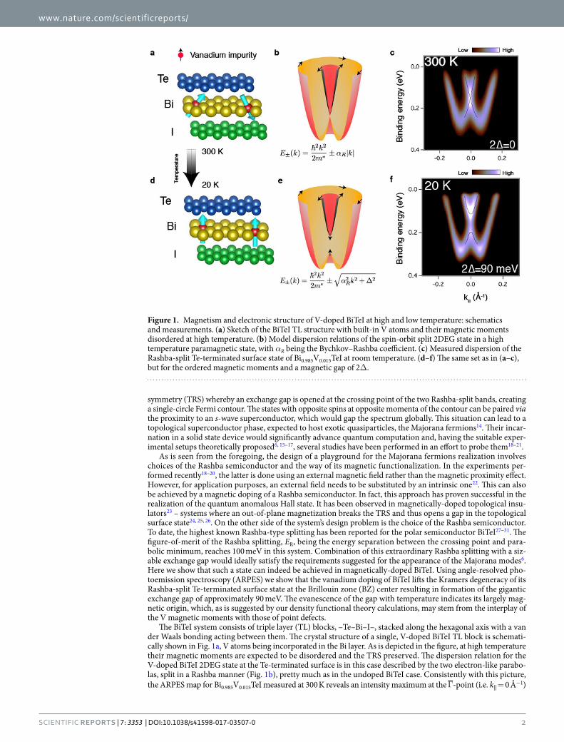
The BiTeI system consists of triple layer (TL) blocks, –Te–Bi–I–, stacked along the hexagonal axis with a van der Waals bonding acting between them. The crystal structure of a single, V-doped BiTeI TL block is schemati-cally shown in Fig. 1a, V atoms being incorporated in the Bi layer. As is depicted in the figure, at high temperature their magnetic moments are expected to be disordered and the TRS preserved. The dispersion relation for the V-doped BiTeI 2DEG state at the Te-terminated surface is in this case described by the two electron-like parabo-las, split in a Rashba manner (Fig. 1b), pretty much as in the undoped BiTeI case. Consistently with this picture, the ARPES map for Bi0.985V0.015TeI measured at 300 K reveals an intensity maximum at the Γ-point (i.e. k|| = 0 Å−1)
Figure 1. Magnetism and electronic structure of V-doped BiTeI at high and low temperature: schematics and measurements. (a) Sketch of the BiTeI TL structure with built-in V atoms and their magnetic moments disordered at high temperature. (b) Model dispersion relations of the spin-orbit split 2DEG state in a high temperature paramagnetic state, with αR being the Bychkov–Rashba coefficient. (c) Measured dispersion of the Rashba-split Te-terminated surface state of Bi0.985V0.015TeI at room temperature. (d–f) The same set as in (a–c), but for the ordered magnetic moments and a magnetic gap of 2Δ.
www.nature.com/scientificreports/
3Scientific RepoRts | 7: 3353 | DOI:10.1038/s41598-017-03507-0
and a binding energy .E 0 15b eV, indicative of the intersection of the parabolas, i.e. the Kramers degeneracy (Fig. 1c).
Assuming an onset of a magnetically ordered state at low temperatures, one may expect the behavior of the Bi0.985V0.015 TeI 2DEG state to change significantly upon cooling down the sample. For instance, if the V magnetic moments were ordered ferromagnetically within the topmost TL and the direction of the moments was perpen-dicular to the surface (see Fig. 1d), the TRS would be broken and the Kramers degeneracy at the Γ-point would be lifted. This behavior can be described by a Hamiltonian that includes the Bychkov–Rashba and exchange terms,
α σ λ σ= + × +⁎H km
m2
(e k) , (1)Rz
z
2 2
z
where m*, αR = 3.8 eVÅ, and λ are the effective electron mass, Rashba coefficient for the undoped BiTeI27, and the strength of the exchange interaction, respectively, while mz is the magnetization, provided by the V atoms. The resulting dispersion relation is then given by
α= ± + ∆± ⁎E k k
mk( )
2, (2)R
2 22 2 2
with Δ = λmz defining the halfwidth of the local gap, which appears between the inner and outer parts of the Rashba-split state, as shown in Fig. 1e. It is precisely this scenario that develops at the Bi0.985V0.015 TeI surface after a cooling down to 20 K, as is evidenced by ARPES measurements reported in Fig. 1f, where the appearance of a giant gap of about 90 meV is clearly seen in the Γ-point.
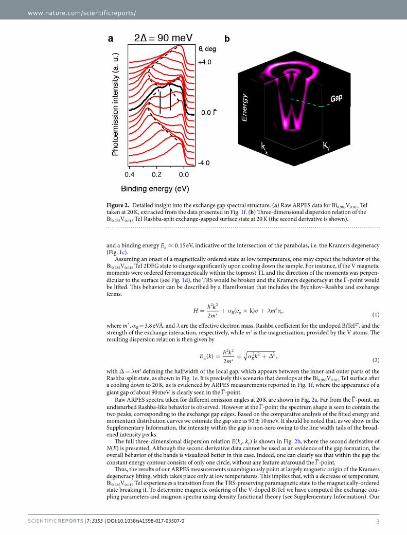
Raw ARPES spectra taken for different emission angles at 20 K are shown in Fig. 2a. Far from the Γ-point, an undisturbed Rashba-like behavior is observed. However at the Γ-point the spectrum shape is seen to contain the two peaks, corresponding to the exchange gap edges. Based on the comparative analysis of the fitted energy and momentum distribution curves we estimate the gap size as 90 ± 10 meV. It should be noted that, as we show in the Supplementary Information, the intensity within the gap is non-zero owing to the line width tails of the broad-ened intensity peaks.
The full three-dimensional dispersion relation E(kx, ky) is shown in Fig. 2b, where the second derivative of N(E) is presented. Although the second derivative data cannot be used as an evidence of the gap formation, the overall behavior of the bands is visualized better in this case. Indeed, one can clearly see that within the gap the constant energy contour consists of only one circle, without any feature at/around the Γ-point.
Thus, the results of our ARPES measurements unambiguously point at largely magnetic origin of the Kramers degeneracy lifting, which takes place only at low temperatures. This implies that, with a decrease of temperature, Bi0.985V0.015 TeI experiences a transition from the TRS-preserving paramagnetic state to the magnetically-ordered state breaking it. To determine magnetic ordering of the V-doped BiTeI we have computed the exchange cou-pling parameters and magnon spectra using density functional theory (see Supplementary Information). Our
Figure 2. Detailed insight into the exchange gap spectral structure. (a) Raw ARPES data for Bi0.985V0.015 TeI taken at 20 K, extracted from the data presented in Fig. 1f. (b) Three-dimensional dispersion relation of the Bi0.985V0.015 TeI Rashba-split exchange-gapped surface state at 20 K (the second derivative is shown).

www.nature.com/scientificreports/
4Scientific RepoRts | 7: 3353 | DOI:10.1038/s41598-017-03507-0
calculations show that although each TL of the V-doped BiTeI is ferromagnetic on its own, the ordering between the adjacent TLs rapidly disappears with the increase of temperature. This, however, does not impede formation of the magnetically ordered state at the surface since the topmost TL is ferromagnetic. These results indicate that it is the topmost FM triple layer that is responsible for the TRS breaking and giant exchange gap opening at the V-doped BiTeI surface.
In order to get deeper insight into the giant exchange gap formation we have performed first-principles surface electronic structure calculations. Since only the magnetism of the topmost TL is essential, we only introduce the dopant into the subsurface Bi layer (see Methods section), which allows us to perform calculations in the low concentration limit. Figure 3a shows the Rashba-split surface state of the Te-terminated undoped BiTeI(0001). It is characterized by a slightly smaller αR than is typically reported in DFT studies30, 32, which is a consequence of a big in-plane supercell choice. However, this is not expected to affect the results and conclusions of the present work (see Supplementary Information). Then, we study the effect of vanadium doping on the Te-terminated BiTeI(0001) surface band structure. One might indeed expect the breakdown of the TRS and, consequently, lifting of the surface state degeneracy at the Γ-point since, being embedded in the Bi layer, a V atom features a magnetic moment of 2.88 μB. Note, that the gapping of the surface states as a consequence of the TRS breaking often assumes induction of the spin polarization on the atoms of a nonmagnetic host by different magnetic agents33, 34. In the case of V-doped BiTeI, the magnetic moments are mainly induced on Te and I atoms, which are located in the immediate vicinity of the V one and have their p-states hybridized with the d-states of the latter. This leads to a lifting of the Rashba-split surface state degeneracy at the 2D BZ center, i.e. to an opening of the exchange gap (Fig. 3b). Surprisingly, the magnitude of the calculated gap of 10 meV turns out to be significantly smaller than that of the measured one.
This means that other factors must be contributing to the formation of the giant exchange gap in the Rashba-split surface state. One of these might be a presence of point defects in the V-doped BiTeI. As a recent scanning tunneling microscopy study shows, there is a large number of point defects seen at both the Te- and I-terminated (0001) surface of the pure BiTeI35. These defects were suggested to be either vacancies or antisites. We suppose that V-doped BiTeI demonstrates a similar situation as long as the dopant concentration is small, which is the case for our samples having rather low V content (0.5 at.%). Therefore, assuming the coexistence of V atoms with point defects, we have separately considered the magnetism of all possible antisites as well as the vacancies in each atomic layer, that have been placed in the topmost Te-terminated TL of the surface of V-doped BiTeI. It turned out that among all the point defects considered, only a Bi vacancy directly induces the host mag-netization (mainly on Te atoms) beyond that caused by the V moments. Moreover, even in the V absence it can supply up to 1.55 μB per a vacancy – a case which is by 7 meV more favorable than the one with a suppressed mag-netization around a vacant site. Our exchange coupling constants calculations show that the magnetic moments appearing on the Te atoms that surround Bi vacancies tend to align antiparallel to those of V atoms, rather insen-sitively to the dopant-vacancy distance (the coupling strength is distance-dependent, though). The Te atoms directly bound to the V one are magnetized antiparallel to its local moment as well. Thus, both V atoms and Bi
Figure 3. Ab initio and tight-binding calculations of pure and V-doped BiTeI. (a) Spin-resolved DFT-calculated (0001) surface band structure of pure BiTeI, projected onto the Te-terminated surface TL block. (b) The same as (a), but for the V-doped BiTeI case. The size of the circles reflects the module of the respective spin projection in each k-point. Note, that in (a) EF is as calculated for the H-passivated slab (see Methods Section). For the clear comparison, in (b) we shift EF to the position corresponding to the undoped case. The artificial discontinuity of the outer branches of the Rashba-split state in b (~|0.1| Å) stems from the crossing with the quantum well state localized in the subsurface TL (see Supplementary Information). (c) Tight-binding calculated surface bandstructure of V-doped BiTeI in the presence of point defect (see Text).

www.nature.com/scientificreports/
5Scientific RepoRts | 7: 3353 | DOI:10.1038/s41598-017-03507-0
vacancies lead to the enhancement of the overall magnetization of the Te layer. It should be noted, however, that the Bi vacancies do not create any magnetic order in the absence of vanadium. On the other hand, their presence increases somewhat the vanadium local moments and enhances the strength of the exchange interaction between them slightly elevating the Curie temperature. Importantly, V doping can facilitate appearance of the Bi vacancies, since their formation energy gets reduced by approximately 0.23 eV in the dopant vicinity.
To see how the additional magnetization induced by the presence of point defects influences the magni-tude of the exchange gap, we have performed band structure calculations with both V and Bivac located in the subsurface atomic layer of BiTeI(0001). However, the results obtained do not allow to unambiguously deter-mine the size of the exchange gap since its edges are broadened due to the Bivac presence (see Supplementary Information). Therefore, to scrutinize the effect of the coexistence of the V dopants and point defects, we resort to a tight-binding approach (see Methods section), where instead of including defects directly, we rather take into account the magnetization they supply. This has been done by introducing an additional Zeeman-like con-tributions to the Hamiltonian, whose values have been set to the exchange splittings of the Bi, Te and I p-states calculated ab initio in the presence of both V dopant and Bi vacancy. The validity of the approach employed has been verified against the DFT result shown in Fig. 3b and the tight-binding description has yielded a gap of sim-ilar magnitude (11 meV).
Figure 3c shows the result of a tight-binding calculation, performed for the case of the V-doped BiTeI in the presence of Bivac. It can be seen that the exchange gap size gets increased appreciably upon accounting for an additional magnetization due to the vacant sites and amounts to 34 meV. This result shows the crucial role, which can play the point defects in the V-doped BiTeI. Note that in real samples the magnetic interplay of point defects and V dopants is probably more intricate than it is theoretically exemplified here. Indeed, in ab initio calculations we have only considered simple point defects. For example, a Bi vacancy has been created by a complete removal of one Bi atom from the cell, and not by its relocation to an interstitial or a surface. Similarly, an antisite atom A has been introduced in a layer B (AB) without leaving behind a vacancy in the layer A or creating the BA antisite which would correspond to the site exchange between atoms A and B. However, in the experimental situation the defects may be complex, as, e.g., a vacancy-antisite pair, proposed for the undoped BiTeI(0001) surface35. Moreover it is not excluded that other complex defects, which have not been observed for the undoped BiTeI case are enabled to form due to V doping. Therefore, further specific and detailed studies, such as scanning tunneling microscopy measurements and simulations, combined with careful theoretical characterization of the observed dopant-defect complexes, are required to uncover missing factors contributing to the formation of the giant exchange gap in the Rashba-split surface state. There is, however, a fundamental reason why the calculated exchange gap size is smaller than the experimentally measured one. The stationary density functional theory is not designed to describe excited state properties and typically underestimates the band gap sizes by 30–70% of the experimental ones36.
Lately, the issue of the Kramers degeneracy lifting observed for the surface states of different bulk-doped systems is under intense discussion9, 24, 37–39. Noteworthy, a 2DEG Rashba-split state with an exchange gap of 90 meV has recently been observed at the SrTiO3 surface38, however the origin of the strong Rashba-like split-ting in this system is not clear yet40. In the case of impurity-doped topological insulators, the Kramers point splitting was experimentally observed9, 24, even at room temperature37, 39. The explanations involving appear-ance of the superparamagnetic clusters37 or a strong resonant scattering due to the dopant in-gap states39 have been put forward. The latter case is particularly interesting since it may lead to the surface state gapping with-out magnetism if a sufficiently strong potential is created by the impurities41. However, this effect would not depend on temperature and, besides, such a perturbation would gap the surface state not only in the Γ-point, but at finite k as well. The results of our ARPES measurements exclude such a scenario, since the gap is seen only in the Γ-point and disappears with the increase of temperature. Another contribution may possibly come from the photoemission process during ARPES measurements of Bi0.985V0.015TeI. Photoexcitation of electrons in V-doped BiTeI by ultraviolet light can induce the spin accumulation at the surface owing to giant spin-orbit interaction. Similar effects had been observed in BiTeI in Refs 31, 42 by laser excitation. Spin accumulation acts like effective magnetic field, and thus, can result in enhancement of the value of the exchange gap at the Γ point.
ConclusionsIn summary, by means of ARPES we have shown that the giant-Rashba-split electronic state residing at the Te-terminated surface of the vanadium-doped polar semiconductor BiTeI exhibits a huge band gap at the Brillouin zone center. Our photoemission measurements, complemented by detailed theoretical calculations, allow to conclude that the origin of this gap largely lies in the time-reversal symmetry breaking, that stems from the magnetically ordered state, onsetting at the vanadium-doped BiTeI surface at low temperature. With this find-ing, magnetically doped BiTeI poses itself as a promising material to be combined with s-wave superconductors with the objective of Majorana fermion formation.
MethodsSingle crystals of BiTeI + 0.5% V were grown using 99.999% pure powders of Bi, Te, I and V by the Bridgman method. ARPES experiments were carried out at Helmholtz-Zentrum Berlin (BESSYII) at beamlines UE112-SGM with the assistance of a Scienta R4000 energy analyzer using synchrotron radiation with the energy of 23 eV. This photon energy allows to obtain the photoelectrons mainly from the surface layers and to avoid the resonant effects appearing due to the Bi 5d levels excitation. The overall energy resolution for the ARPES measurements was 5 meV. Samples were cleaved insitu at the base pressure of 6 × 10⁻¹¹ mbar. In order to check the contami-nation of the surface, the cooling down to 20 K had been done both before and after the cleavages. Part of the

www.nature.com/scientificreports/
6Scientific RepoRts | 7: 3353 | DOI:10.1038/s41598-017-03507-0
experiments were performed out in the Research Resource Center “Physical methods of surface investigation” of Saint Petersburg State University. The crystalline order and cleanliness of the surface were verified by low energy electron diffraction (LEED) and X-ray photoelectron spectroscopy (XPS).
Ab initio calculations were performed using the density functional theory in the generalized gradient approximation to the exchange-correlation potential43. The localized V 3d-states were described in the frame-work of the GGA + U approach44, with an effective U − J value of 3 eV (Dudarev’s scheme45). Surface electronic structure calculations were performed within the projector augmented-wave method46 in the VASP implemen-tation47, 48. The Hamiltonian contained the scalar relativistic corrections and the spin-orbit coupling was taken into account by the second variation method49. In order describe the van der Waals interactions we made use of DFT-D2 approach proposed by Grimme50. We set the energy cutoff for the plane-wave expansion of wave functions to be equal to 250 eV and chose a Γ-centered k-point grid of 3 × 3 × 1 to sample the two-dimensional Brillouin zone. The (0001) surface of V-doped BiTeI was simulated by a 3TL-thick slab and (3 × 3) hexagonal in-plane supercell with 9 atoms per single layer. Vanadium atom and/or Bi vacancy were placed in the surface TL, which is terminated by Te atoms. The doping of the subsurface TL wasn’t considered since the Rashba-split state at Te-terminated BiTeI(0001) resides predominantly in the topmost TL block. Thus the V concentration in our calculations was of about 1.23%. Upon introduction of V atom and Bi vacancy, a structural optimization was performed using a conjugate-gradient algorithm and a force tolerance criterion for convergence of 0.05 eV/Å. Vanadium’s magnetic moment was directed out-of-plane, i.e. perpendicular to the surface. As far as the iodine surface is concerned, it was passivated by placing a hydrogen atom on top of each iodine one. All calculations were performed using a model of repeating slabs separated by a vacuum gap of a minimum of 10 Å.
Magnetic ordering of the V-doped BiTeI was studied using the Korringa-Kohn-Rostoker method51, 52 within a full potential approximation to the crystal potential53. Final concentration of the V atoms and Bi vacancies was accounted for using the coherent potential approach as it is implemented within the multiple scattering theory54. We took an angular momentum cutoff of lmax = 3 for the Green’s function and a k-point mesh of 50 × 50 × 50 (50 × 50 × 1) for the 3D (2D) Brillouin zone integration.
Ab-initio-based tight-binding calculations were performed using the VASP package with the WANNIER90 interface55, 56. The wannier basis chosen consists of six spinor p-type orbitals >↑px , | >↑py , | >↑pz , >↓px , | >↓py , | >↓pz for each atom, while the low-lying s orbitals were not taken into consideration. The band-bending potential was obtained from previous DFT calculations57. A Zeeman term in Eq. (2) was set to the exchange splitting of the Bi, Te and I p-states, as calculated within a scalar-relativistic approach. The surface band structure was calculated for the semi-infinite system within the Green function approach58, 59.
References 1. Klitzing, K. V., Dorda, G. & Pepper, M. New method for high-accuracy determination of the fine-structure constant based on
quantized hall resistance. Physical Review Letters 45, 494–497, doi:10.1103/PhysRevLett.45.494 (1980). 2. Bernevig, B. A. & Zhang, S.-C. Quantum Spin Hall Effect. Physical Review Letters 96, 106802, doi:10.1103/PhysRevLett.96.106802
(2006). 3. Onoda, M. & Nagaosa, N. Quantized Anomalous Hall Effect in Two-Dimensional Ferromagnets: Quantum Hall Effect in Metals.
Physical Review Letters 90, 206601, doi:10.1103/PhysRevLett.90.206601 (2003). 4. Krupin, O. et al. Rashba effect at magnetic metal surfaces. Physical Review B 71, 201403, doi:10.1103/PhysRevB.71.201403 (2005). 5. Qi, X.-L., Hughes, T. L. & Zhang, S.-C. Topological field theory of time-reversal invariant insulators. Phys. Rev. B 78, 195424,
doi:10.1103/PhysRevB.78.195424 (2008). 6. Sau, J. D., Lutchyn, R. M., Tewari, S. & Das Sarma, S. Generic new platform for topological quantum computation using
semiconductor heterostructures. Phys. Rev. Lett. 104, 040502, doi:10.1103/PhysRevLett.104.040502 (2010). 7. Fert, A., Cros, V. & Sampaio, J. Skyrmions on the track. Nature nanotechnology 8, 152–156, doi:10.1038/nnano.2013.29 (2013). 8. Liu, J. et al. Competition between Rashba Effect and Exchange Interaction in a Hg0.98 Mn0.02 Te Magnetic 2DEG. Journal of
Superconductivity: Incorporating Novel Magnetism 16, 365–368, doi:10.1023/A:1023638125071 (2003). 9. Xu, S.-Y. et al. Hedgehog spin texture and Berry’s phase tuning in a magnetic topological insulator. Nat Phys 8, 616–622, doi:10.1038/
nphys2351 (2012). 10. Henk, J. et al. Topological character and magnetism of the Dirac state in Mn-doped Bi2Te3. Phys. Rev. Lett. 109, 076801, doi:10.1103/
PhysRevLett.109.076801 (2012). 11. Liu, Q., Liu, C.-X., Xu, C., Qi, X.-L. & Zhang, S.-C. Magnetic impurities on the surface of a topological insulator. Phys. Rev. Lett. 102,
156603, doi:10.1103/PhysRevLett.102.156603 (2009). 12. Yu, R. et al. Quantized anomalous hall effect in magnetic topological insulators. Science 329, 61–64, doi:10.1126/science.1187485
(2010). 13. Bychkov, Y. A. & Rashba, E. I. Properties of a 2D electron gas with lifted spectral degeneracy. JETP Letters 39, 78–81 (1984). 14. Kitaev, A. Y. Unpaired majorana fermions in quantum wires. Physics-Uspekhi 44, 131–136, doi:10.1070/1063-7869/44/10S/S29
(2001). 15. Fu, L. & Kane, C. L. Superconducting proximity effect and majorana fermions at the surface of a topological insulator. Phys. Rev. Lett.
100, 096407, doi:10.1103/PhysRevLett.100.096407 (2008). 16. Alicea, J., Oreg, Y., Refael, G., von Oppen, F. & Fisher, M. P. A. Non-abelian statistics and topological quantum information
processing in 1D wire networks. Nat Phys 7, 412–417, doi:10.1103/PhysRevLett.107.236401 (2011). 17. Nadj-Perge, S., Drozdov, I. K., Bernevig, B. A. & Yazdani, A. Proposal for realizing majorana fermions in chains of magnetic atoms
on a superconductor. Phys. Rev. B 88, 020407–7, doi:10.1103/PhysRevB.88.020407 (2013). 18. Mourik, V. et al. Signatures of Majorana fermions in hybrid superconductor-semiconductor nanowire devices. Science 336,
1003–1007, doi:10.1126/science.1222360 (2012). 19. Das, A. et al. Zero-bias peaks and splitting in an Al-InAs nanowire topological superconductor as a signature of Majorana fermions.
Nature Physics 8, 887–895, doi:10.1038/nphys2479 (2012). 20. Deng, M. T. et al. Anomalous zero-bias conductance peak in a NbNb hybrid device. Nano Letters 12, 6414–6419, doi:10.1021/
nl303758w. PMID: 23181691 (2012). 21. Nadj-Perge, S. et al. Observation of Majorana fermions in ferromagnetic atomic chains on a superconductor. Science 346, 602–607,
doi:10.1126/science.1259327 (2014).

www.nature.com/scientificreports/
7Scientific RepoRts | 7: 3353 | DOI:10.1038/s41598-017-03507-0
22. He, K., Wang, Y. & Xue, Q.-K. Quantum anomalous Hall effect. National Science Review 1, 38–40, doi:10.1093/nsr/nwt029 (2014).
23. Chang, C.-Z. et al. Experimental observation of the quantum anomalous Hall effect in a magnetic topological insulator. Science 340, 167–170, doi:10.1126/science.1234414 (2013).
24. Chen, Y. L. et al. Massive Dirac fermion on the surface of a magnetically doped topological insulator. Science 329, 659–662, doi:10.1126/science.1189924 (2010).
25. Checkelsky, J. G., Ye, J., Onose, Y., Iwasa, Y. & Tokura, Y. Dirac-fermion-mediated ferromagnetism in a topological insulator. Nature Physics 8, 729–733, doi:10.1038/nphys2388 (2012).
26. Otrokov, M. M., Menshchikova, T. V., Vergniory, M. G., Rusinov, I. P., Vyazovskaya, A. Yu., Koroteev, Yu. M., Bihlmayer, G., Ernst, A., Echenique, P. M., Arnau, A. & Chulkov, E. V. Highly-ordered wide bandgap materials for quantized anomalous Hall and magnetoelectric effects. 2D Materials 4, 025082, doi:10.1088/2053-1583/aa6bec (2017).
27. Ishizaka, K. et al. Giant Rashba-type spin splitting in bulk BiTeI. Nature materials 10, 521–526, doi:10.1038/nmat3051 (2011). 28. Landolt, G. et al. Disentanglement of surface and bulk Rashba spin splittings in noncentrosymmetric BiTeI. Physical Review Letters
109, 116403, doi:10.1103/PhysRevLett.109.116403 (2012). 29. Crepaldi, A. et al. Giant ambipolar Rashba effect in the semiconductor BiTeI. Phys. Rev. Lett. 109, 096803, doi:10.1103/
PhysRevLett.109.096803 (2012). 30. Eremeev, S. V., Nechaev, I. A., & Chulkov, E. V. Giant Rashba-type spin splitting at polar surfaces of BiTeI. JETP Letters 96, 437–444,
doi:10.1134/S0021364012190071 (2012). 31. Ogawa, N., Bahramy, M. S., Murakawa, H., Kaneko, Y. & Tokura, Y. Magnetophotocurrent in BiTeI with Rashba spin-split bands.
Physical Review B 88, 035130, doi:10.1103/PhysRevB.88.035130 (2013). 32. Eremeev, S. V., Nechaev, I. A., Koroteev, Y. M., Echenique, P. M. & Chulkov, E. V. Ideal two-dimensional electron systems with a giant
Rashba-type spin splitting in real materials: Surfaces of bismuth tellurohalides. Phys. Rev. Lett. 108, 246802, doi:10.1103/PhysRevLett.108.246802 (2012).
33. Eremeev, S. V., Men’shov, V. N., Tugushev, V. V., Echenique, P. M. & Chulkov, E. V. Magnetic proximity effect at the three-dimensional topological insulator/magnetic insulator interface. Phys. Rev. B 88, 144430, doi:10.1103/PhysRevB.88.144430 (2013).
34. Otrokov, M. M., Chulkov, E. V. & Arnau, A. Breaking time-reversal symmetry at the topological insulator surface by metal-organic coordination networks. Phys. Rev. B 92, 165309, doi:10.1103/PhysRevB.92.165309 (2015).
35. Fiedler, S. et al. Defect and structural imperfection effects on the electronic properties of BiTeI surfaces. New Journal of Physics 16, 075013, doi:10.1088/1367-2630/16/7/075013 (2014).
36. Hedin, L. On correlation effects in electron spectroscopies and the QW approximation. J. Phys.: Condens. Matter 11, R489 (1999).
37. Chang, C.-Z. et al. Chemical-potential-dependent gap opening at the Dirac surface states of Bi2Se3 induced by aggregated substitutional Cr atoms. Phys. Rev. Lett. 112, 056801, doi:10.1103/PhysRevLett.112.056801 (2014).
38. Santander-Syro, A. F. et al. Giant spin splitting of the two-dimensional electron gas at the surface of SrTiO3. Nature Materials 13, 1085–1090, doi:10.1038/nmat4107 (2014).
39. Sanchez-Barriga, J. et al. Nonmagnetic band gap at the Dirac point of the magnetic topological insulator (Bi1−x Mnx)2 Se3. Nat Commun 7 (2016).
40. Garcia-Castro, A. C., Vergniory, M. G., Bousquet, E. & Romero, A. H. Spin texture induced by oxygen vacancies in strontium perovskite (001) surfaces: A theoretical comparison between SrTiO3 and SrHfO3. Phys. Rev. B 93, 045405, doi:10.1103/PhysRevB.93.045405 (2016).
41. Black-Schaffer, A. M. & Balatsky, A. V. Subsurface impurities and vacancies in a three-dimensional topological insulator. Phys. Rev. B 86, 115433, doi:10.1103/PhysRevB.86.115433 (2012).
42. Ogawa, N., Bahramy, M. S., Kaneko, Y. & Tokura, Y. Photocontrol of Dirac electrons in a bulk Rashba semiconductor. Physical Review B 90, 1–6, doi:10.1103/PhysRevB.90.125122 (2014).
43. Perdew, J. P., Burke, K. & Ernzerhof, M. Generalized gradient approximation made simple. Phys. Rev. Lett. 77, 3865–3868, doi:10.1103/PhysRevLett.77.3865 (1996).
44. Anisimov, V. I., Zaanen, J. & Andersen, O. K. Band theory and Mott insulators: Hubbard U instead of stoner. I. Phys. Rev. B 44, 943–954, doi:10.1103/PhysRevB.44.943 (1991).
45. Dudarev, S. L., Botton, G. A., Savrasov, S. Y., Humphreys, C. J. & Sutton, A. P. Electron-energy-loss spectra and the structural stability of nickel oxide: An LSDA + U study. Phys. Rev. B 57, 1505–1509, doi:10.1103/PhysRevB.57.1505 (1998).
46. Blöchl, P. E. Projector augmented-wave method. Phys. Rev. B 50, 17953–17979, doi:10.1103/PhysRevB.50.17953 (1994). 47. Kresse, G. & Furthmüller, J. Efficiency of ab-initio total energy calculations for metals and semiconductors using a plane-wave basis
set. Comp. Mat. Sci. 6, 15–50, doi:10.1016/0927-0256(96)00008-0 (1996). 48. Hafner, J. Ab-initio simulations of materials using VASP: Density-functional theory and beyond. J. Comp. Chem. 29, 2044–2078,
doi:10.1002/jcc.v29:13 (2008). 49. Koelling, D. D. & Harmon, B. N. A technique for relativistic spin-polarised calculations. J. Phys. C: Sol. St. Phys 10, 3107–3114,
doi:10.1088/0022-3719/10/16/019 (1977). 50. Grimme, S. Semiempirical GGA-type density functional constructed with a long-range dispersion correction. Journal Of
Computational Chemistry 27, 1787–1799, doi:10.1002/jcc.20495 (2006). 51. Korringa, J. On the calculation of the energy of a bloch wave in a metal. Physica 13, 392–400, doi:10.1016/0031-8914(47)90013-X
(1947). 52. Kohn, W. & Rostoker, N. Solution of the schrödinger equation in periodic lattices with an application to metallic lithium. Phys. Rev.
94, 1111–1120, doi:10.1103/PhysRev.94.1111 (1954). 53. M. Geilhufe, S. A. et al. Numerical solution of the relativistic single-site scattering problem for the coulomb and the Mathieu
potential. J. Phys.: Condens. Matter 27, 435202 (2015). 54. Gyorffy, B. L. Coherent-potential approximation for a nonoverlapping-muffin-tin-potential model of random substitutional alloys.
Phys. Rev. B 5, 2382–2384, doi:10.1103/PhysRevB.5.2382 (1972). 55. Marzari, N. & Vanderbilt, D. Maximally localized generalized Wannier functions for composite energy bands. Phys. Rev. B 56,
12847–12865, doi:10.1103/PhysRevB.56.12847 (1997). 56. Mostofi, A. A. et al. Wannier90: A tool for obtaining maximally-localised Wannier functions. Computer Physics Communications
178, 685–699, doi:10.1016/j.cpc.2007.11.016 (2008). 57. Eremeev, S., Rusinov, I., Nechaev, I. & Chulkov, E. Rashba split surface states in BiTeBr. New Journal of Physics 15, 075015,
doi:10.1088/1367-2630/15/7/075015 (2013). 59. Sancho, M. L., Sancho, J. L. & Rubio, J. Highly convergent schemes for the calculation of bulk and surface green functions. J. Phys. F
15, 851–858, doi:10.1088/0305-4608/15/4/009 (1985). 59. Henk, J. & Schattke, W. A subroutine package for computing Green’s functions of relaxed surfaces by the renormalization method.
Comput. Phys. Commun. 77, 69–83, doi:10.1016/0010-4655(93)90038-E (1993).

www.nature.com/scientificreports/
8Scientific RepoRts | 7: 3353 | DOI:10.1038/s41598-017-03507-0
AcknowledgementsThe work was partially supported by grant of Saint Petersburg State University for scientific investigations (N. 15.61.202.2015). This study was supported by the Russian Science Foundation (project N. 17-12-01047, in part of crystal growth, structural characterization and ARPES measurements (Figs 1, 2)). The funding by the University of the Basque Country (Grant Nos GIC07IT36607 and IT-756-13), the Spanish Ministry of Science and Innovation (Grant Nos FIS2013-48286-C02-02-P, FIS2013-48286-C02-01-P, and FIS2016-75862-P) and Tomsk State University Academic D.I. Mendeleev Fund Program in 2015 (research grant N 8.1.05.2015) are also gratefully acknowledged. The authors also acknowledge support from the Russian-German laboratory at BESSY II, the “German-Russian Interdisciplinary Science Center”(G-RISC) program and the Impuls- und Vernetzungsfonds der Helmholtz-Gemeinschaft (Grant No. HRJRG-408). The calculations were performed on the SKIF-Cyberia supercomputer at Tomsk State University (Russia).
Author ContributionsThe project was proposed by E.V.C., O.E.T., and A.M.S. The measurements were performed by I.I.K., A.M.S., O.E.T., V.A.G., J.S.-B., A.V., and O.R. Samples were grown and caracterized by O.E.T., V.A.G., and K.A.K. The experimental data analysis was carried out by I.I.K., O.E.T., and A.M.S. DFT and tight-binding calculations were performed by M.M.O., A.E., I.P.R., and E.V.C. All authors extensively discussed the results and parcitipated in the manuscript editing. The manuscript was written by I.I.K. and M.M.O.
Additional InformationSupplementary information accompanies this paper at doi:10.1038/s41598-017-03507-0Competing Interests: The authors declare that they have no competing interests.Publisher's note: Springer Nature remains neutral with regard to jurisdictional claims in published maps and institutional affiliations.
Open Access This article is licensed under a Creative Commons Attribution 4.0 International License, which permits use, sharing, adaptation, distribution and reproduction in any medium or
format, as long as you give appropriate credit to the original author(s) and the source, provide a link to the Cre-ative Commons license, and indicate if changes were made. The images or other third party material in this article are included in the article’s Creative Commons license, unless indicated otherwise in a credit line to the material. If material is not included in the article’s Creative Commons license and your intended use is not per-mitted by statutory regulation or exceeds the permitted use, you will need to obtain permission directly from the copyright holder. To view a copy of this license, visit http://creativecommons.org/licenses/by/4.0/. © The Author(s) 2017