Getting Started with the MSP430 LaunchPad
106
Getting Started with the MSP430 LaunchPad Version 2.01
description
Getting Started with the MSP430 LaunchPad. Version 2.01. Agenda. Introduction to Value Line Code Composer Studio Initialization and GPIO Analog-to-Digital Converter Interrupts and the Timer Low-Power Optimization Serial Communications Grace FRAM Optional: Capacitive Touch. - PowerPoint PPT Presentation
Transcript of Getting Started with the MSP430 LaunchPad
Getting Started with the MSP430 LaunchPad
Version 2.01

Agenda
Introduction to Value LineCode Composer StudioInitialization and GPIO
Analog-to-Digital ConverterInterrupts and the TimerLow-Power OptimizationSerial Communications
GraceFRAM
Optional: Capacitive Touch
Portfolio …2
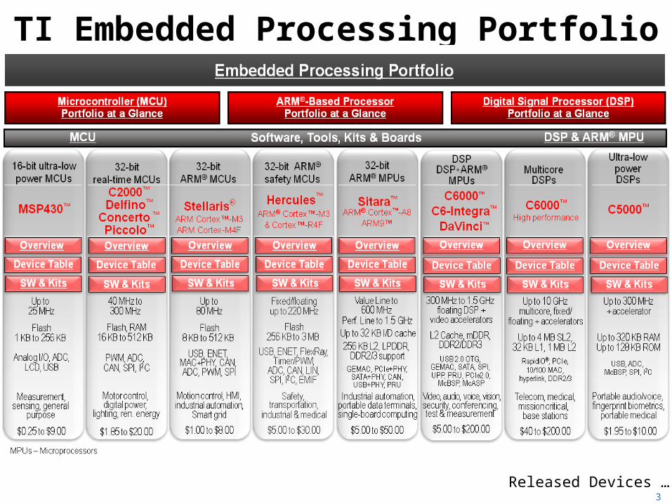
TI Embedded Processing Portfolio
Released Devices …3
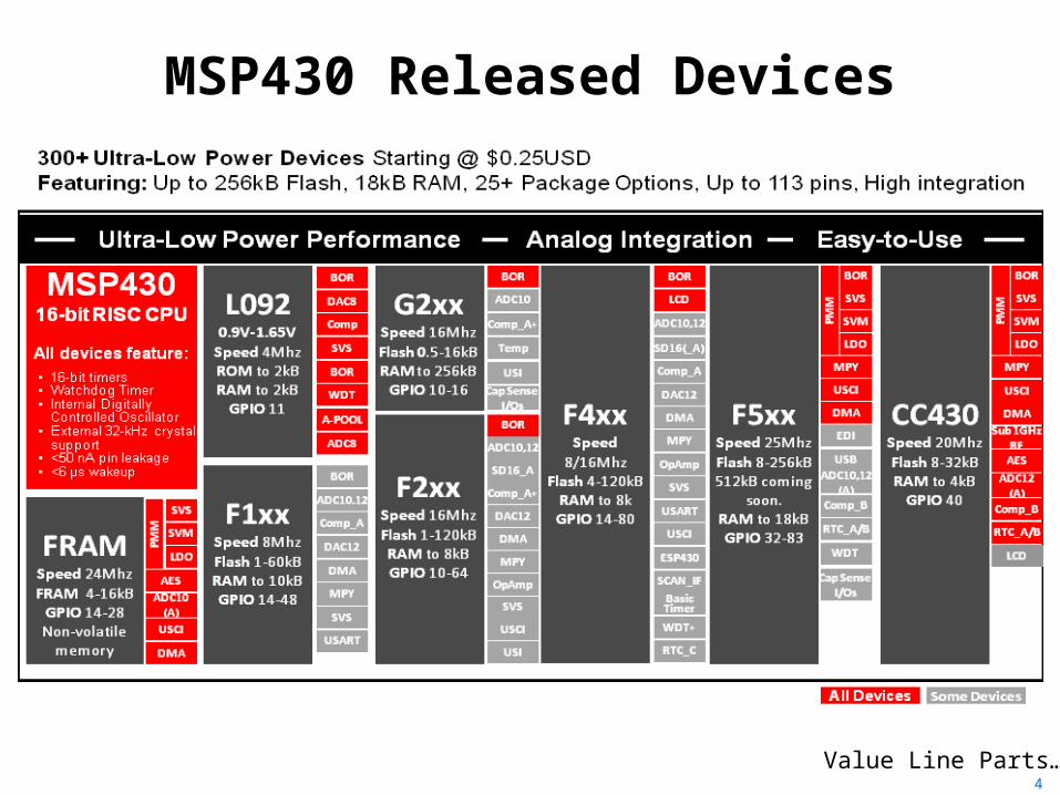
MSP430 Released Devices
Value Line Parts…4
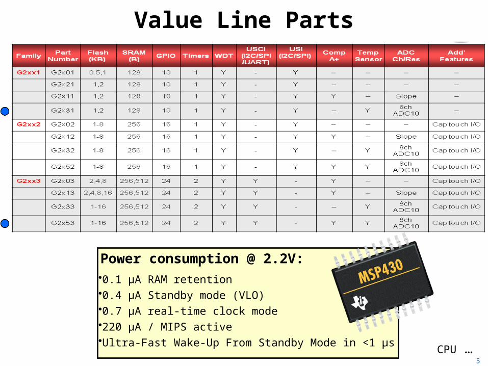
Value Line Parts
•0.1 μA RAM retention•0.4 μA Standby mode (VLO)•0.7 μA real-time clock mode•220 μA / MIPS active•Ultra-Fast Wake-Up From Standby Mode in <1 μs
Power consumption @ 2.2V:
CPU …5
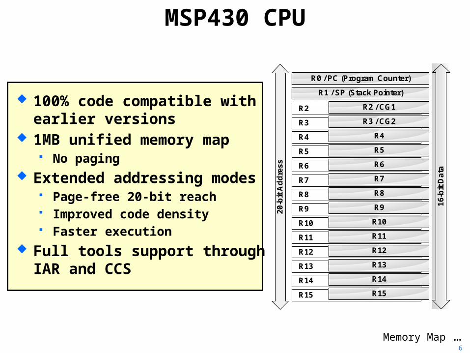
MSP430 CPU
100% code compatible withearlier versions
1MB unified memory map No paging
Extended addressing modes Page-free 20-bit reach Improved code density Faster execution
Full tools support throughIAR and CCS
R2
R3
R4
R5
R7
R8
R10
R9
R11
R12
R13
R6
R14
R15
R0 / PC (Program Counter)
R1 / SP (Stack Pointer)
R2 / CG1
R3 / CG2
R4
R5
R7
R8
R10
R9
R11
R12
R13
R6
R14
R1520
-bit
Add
ress
16-b
it D
ata
Memory Map …6
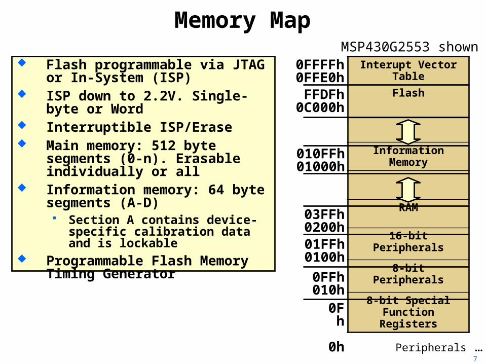
Memory MapInterupt Vector Table
Flash
InformationMemory
RAM
16-bitPeripherals
8-bitPeripherals
8-bit Special FunctionRegisters
Flash programmable via JTAG or In-System (ISP)
ISP down to 2.2V. Single-byte or Word
Interruptible ISP/Erase Main memory: 512 byte segments
(0-n). Erasable individually or all Information memory: 64 byte
segments (A-D) Section A contains device-specific
calibration data and is lockable Programmable Flash Memory
Timing Generator
0Fh
0h
0FFh010h
01FFh0100h
03FFh0200h
FFDFh0C000h
0FFFFh0FFE0h
Peripherals …
MSP430G2553 shown
010FFh01000h
7
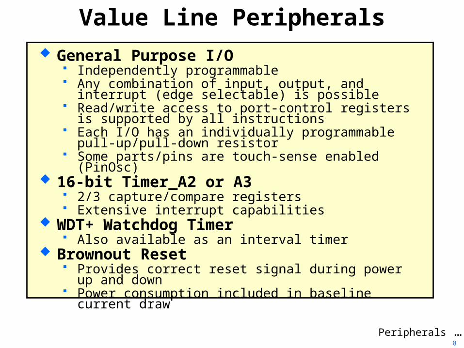
Value Line Peripherals General Purpose I/O
Independently programmable Any combination of input, output, and interrupt (edge
selectable) is possible Read/write access to port-control registers is supported by
all instructions Each I/O has an individually programmable pull-up/pull-
down resistor Some parts/pins are touch-sense enabled (PinOsc)
16-bit Timer_A2 or A3 2/3 capture/compare registers Extensive interrupt capabilities
WDT+ Watchdog Timer Also available as an interval timer
Brownout Reset Provides correct reset signal during power up and down Power consumption included in baseline current draw
Peripherals …8
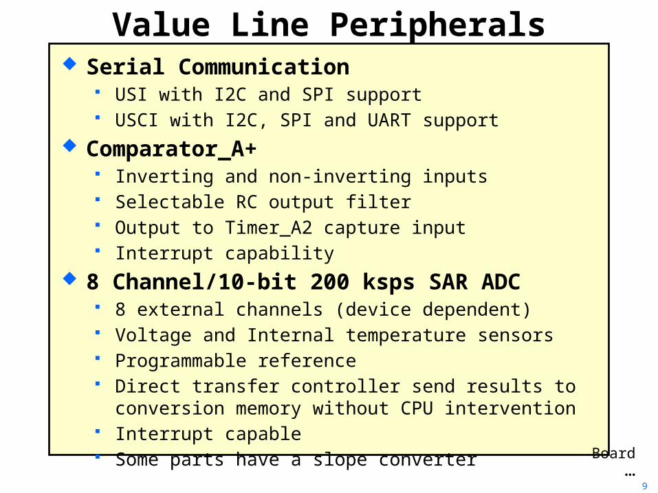
Value Line Peripherals Serial Communication
USI with I2C and SPI support USCI with I2C, SPI and UART support
Comparator_A+ Inverting and non-inverting inputs Selectable RC output filter Output to Timer_A2 capture input Interrupt capability
8 Channel/10-bit 200 ksps SAR ADC 8 external channels (device dependent) Voltage and Internal temperature sensors Programmable reference Direct transfer controller send results to conversion memory
without CPU intervention Interrupt capable Some parts have a slope converter Board
…9
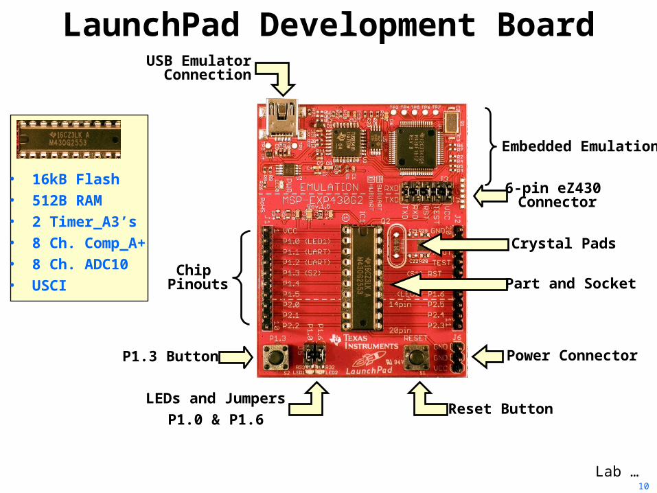
LaunchPad Development Board
Embedded Emulation
6-pin eZ430 Connector
Part and Socket
Crystal Pads
Power Connector
Reset ButtonLEDs and Jumpers
P1.0 & P1.6
P1.3 Button
Chip Pinouts
USB EmulatorConnection
Lab …
• 16kB Flash• 512B RAM• 2 Timer_A3’s• 8 Ch. Comp_A+• 8 Ch. ADC10• USCI
10
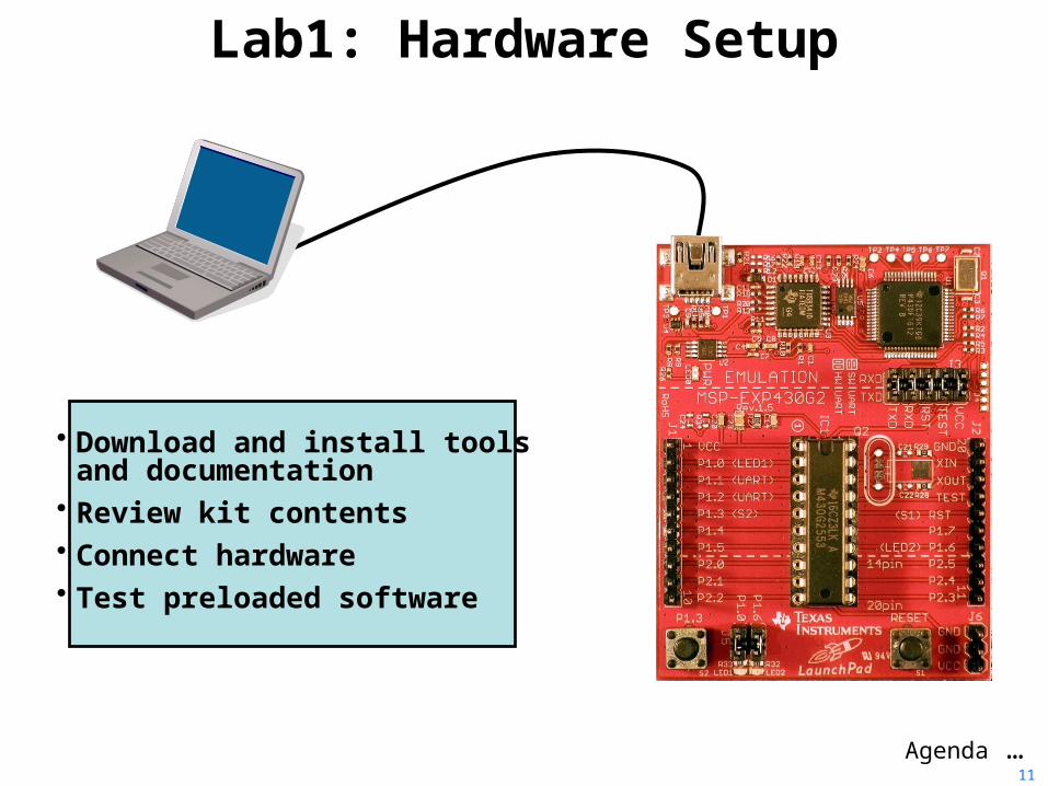
Lab1: Hardware Setup
• Download and install toolsand documentation
• Review kit contents• Connect hardware• Test preloaded software
Agenda …11

Agenda
Introduction to Value LineCode Composer StudioInitialization and GPIO
Analog-to-Digital ConverterInterrupts and the TimerLow-Power OptimizationSerial Communications
GraceFRAM
Optional: Capacitive Touch
12
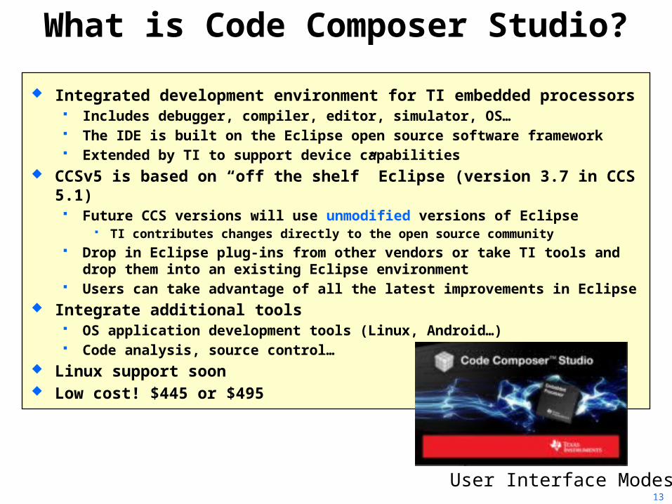
What is Code Composer Studio?
Integrated development environment for TI embedded processors Includes debugger, compiler, editor, simulator, OS… The IDE is built on the Eclipse open source software framework Extended by TI to support device capabilities
CCSv5 is based on “off the shelf” Eclipse (version 3.7 in CCS 5.1) Future CCS versions will use unmodified versions of Eclipse
TI contributes changes directly to the open source community Drop in Eclipse plug-ins from other vendors or take TI tools and drop them
into an existing Eclipse environment Users can take advantage of all the latest improvements in Eclipse
Integrate additional tools OS application development tools (Linux, Android…) Code analysis, source control…
Linux support soon Low cost! $445 or $495
User Interface Modes…13
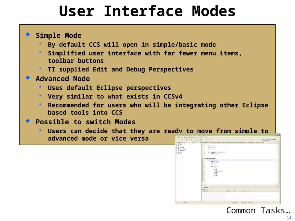
User Interface Modes Simple Mode
By default CCS will open in simple/basic mode Simplified user interface with far fewer menu items, toolbar buttons TI supplied Edit and Debug Perspectives
Advanced Mode Uses default Eclipse perspectives Very similar to what exists in CCSv4 Recommended for users who will be integrating other Eclipse based
tools into CCS Possible to switch Modes
Users can decide that they are ready to move from simple to advanced mode or vice versa
Common Tasks…14
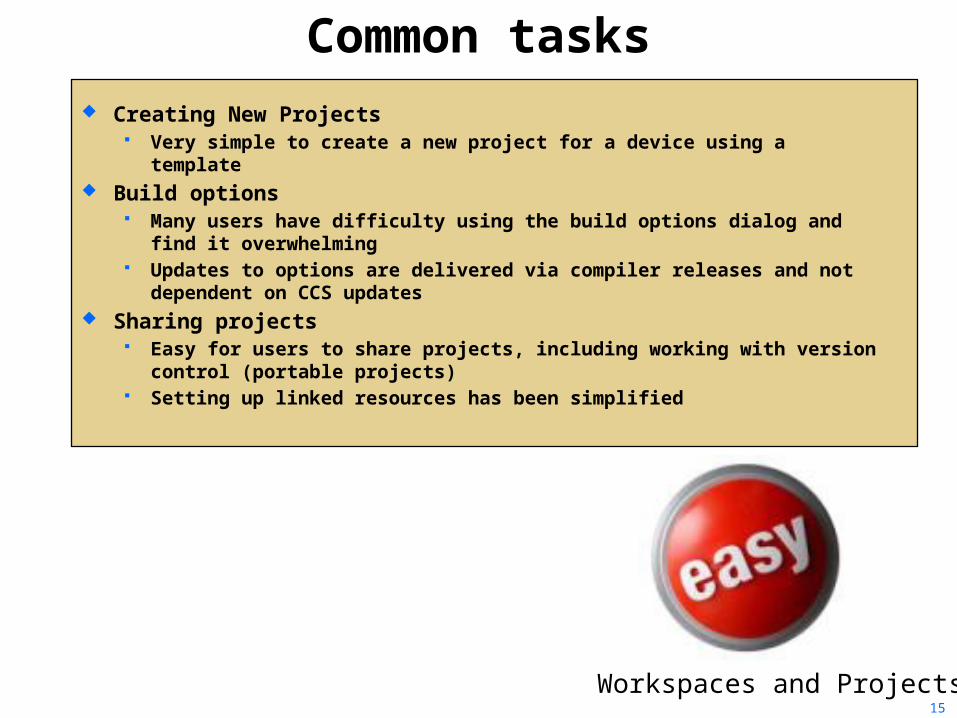
Common tasks Creating New Projects
Very simple to create a new project for a device using a template Build options
Many users have difficulty using the build options dialog and find it overwhelming
Updates to options are delivered via compiler releases and not dependent on CCS updates
Sharing projects Easy for users to share projects, including working with version control
(portable projects) Setting up linked resources has been simplified
Workspaces and Projects…15
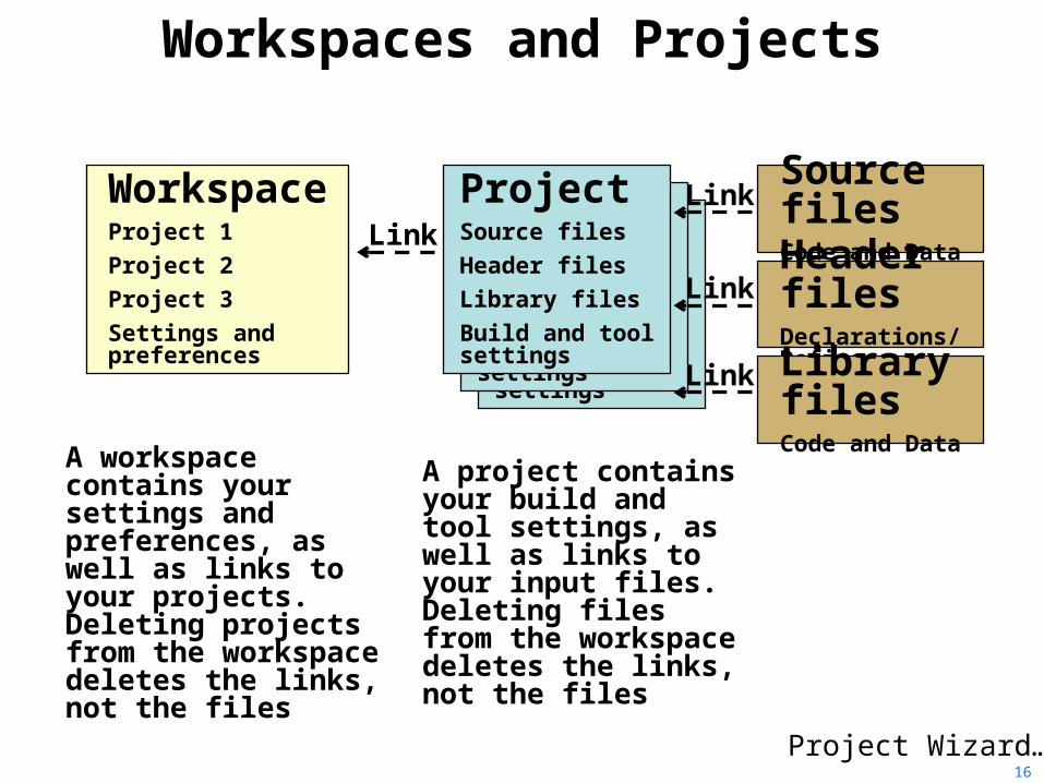
ProjectSource filesHeader FilesLibrary filesBuild and tool settings
ProjectSource filesHeader FilesLibrary filesBuild and tool settings
Workspaces and Projects
WorkspaceProject 1Project 2Project 3Settings and preferences
A workspace contains your settings and preferences, as well as links to your projects. Deleting projects from the workspace deletes the links, not the files
ProjectSource filesHeader filesLibrary filesBuild and tool settings
A project contains your build and tool settings, as well as links to your input files. Deleting files from the workspace deletes the links, not the files
Source filesCode and Data
Header filesDeclarations/Defines
Library filesCode and Data
LinkLink
Link
Link
Project Wizard…16
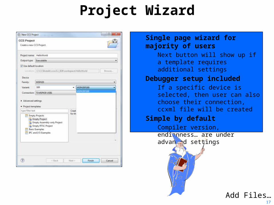
Project Wizard Single page wizard for majority of
users Next button will show up if a template
requires additional settings Debugger setup included
If a specific device is selected, then user can also choose their connection, ccxml file will be created
Simple by default Compiler version, endianness… are
under advanced settings
Add Files…17
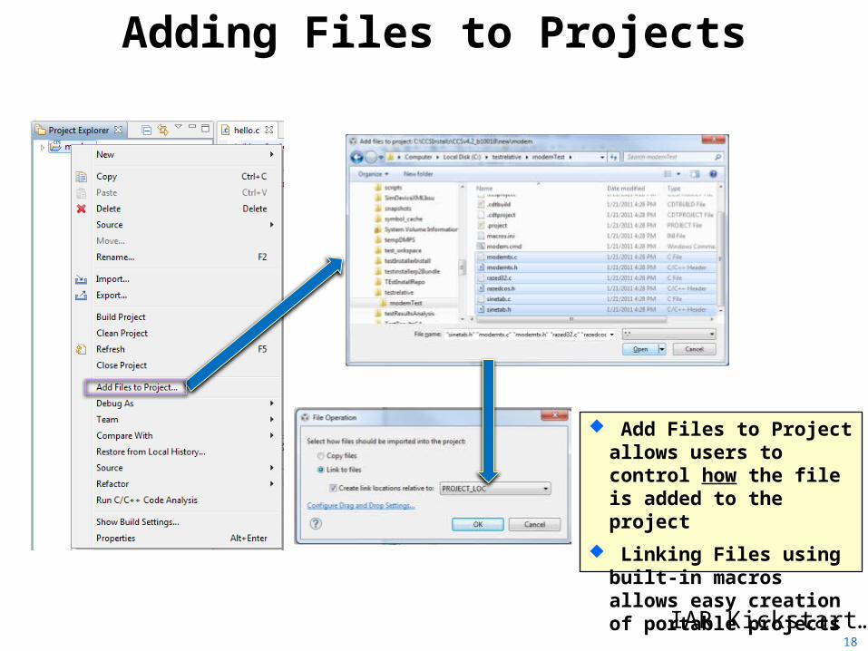
Adding Files to Projects
Add Files to Project allows users to control how the file is added to the project
Linking Files using built-in macros allows easy creation of portable projects
IAR Kickstart…18
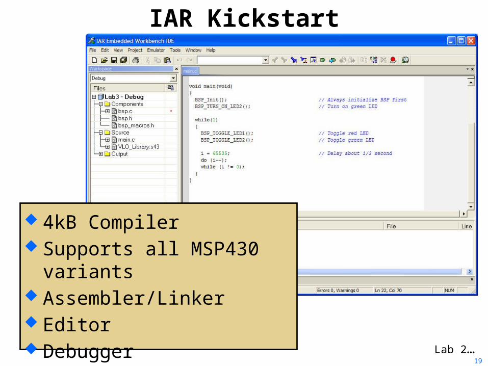
IAR Kickstart
4kB Compiler Supports all MSP430 variants Assembler/Linker Editor Debugger
Lab 2…19
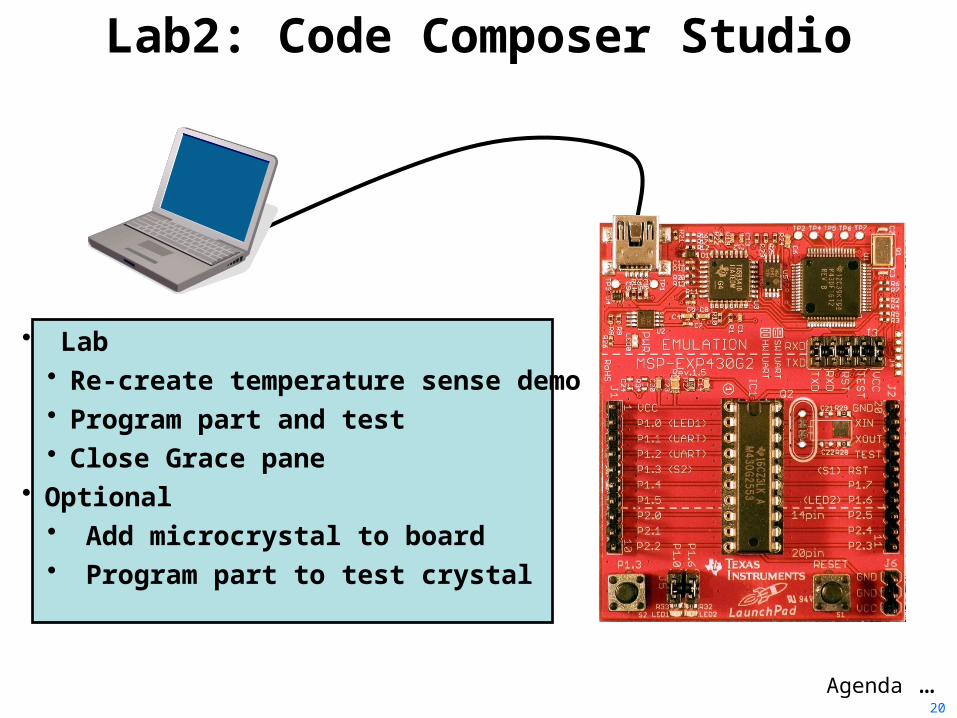
Lab2: Code Composer Studio
Agenda …
• Lab• Re-create temperature sense demo• Program part and test• Close Grace pane
• Optional• Add microcrystal to board• Program part to test crystal
20
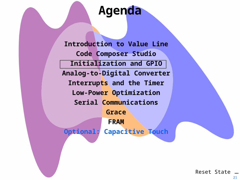
Agenda
Reset State …
Introduction to Value LineCode Composer StudioInitialization and GPIO
Analog-to-Digital ConverterInterrupts and the TimerLow-Power OptimizationSerial Communications
GraceFRAM
Optional: Capacitive Touch
21
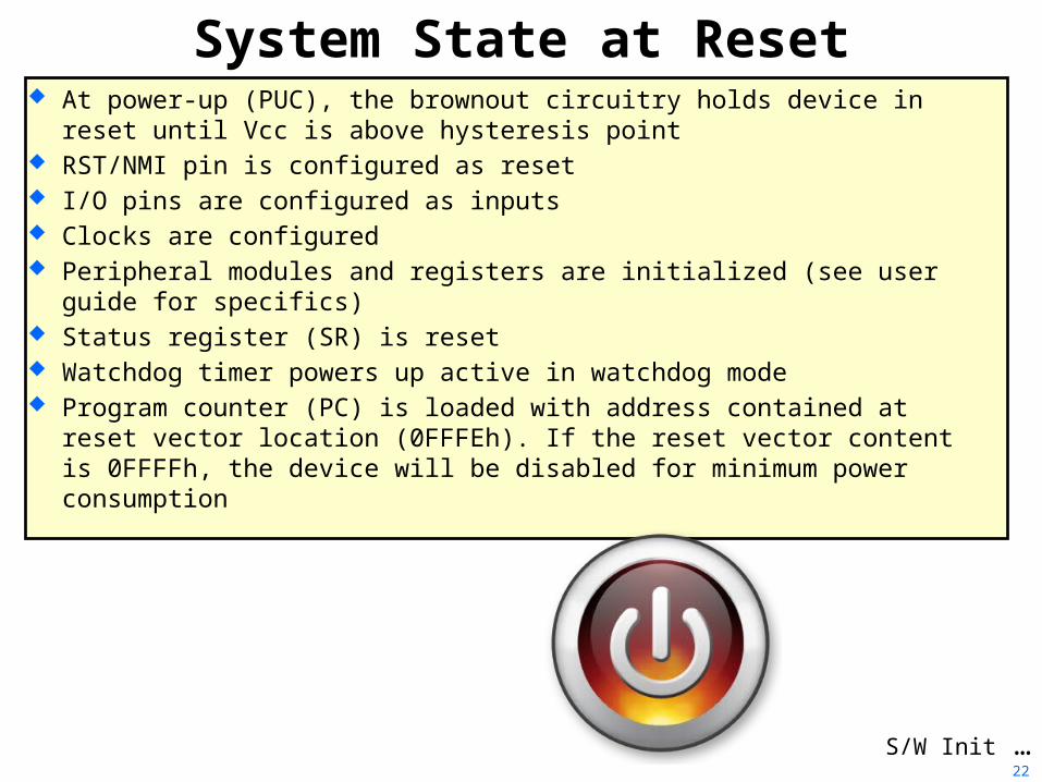
System State at Reset At power-up (PUC), the brownout circuitry holds device in reset until Vcc is
above hysteresis point RST/NMI pin is configured as reset I/O pins are configured as inputs Clocks are configured Peripheral modules and registers are initialized (see user guide for specifics) Status register (SR) is reset Watchdog timer powers up active in watchdog mode Program counter (PC) is loaded with address contained at reset vector
location (0FFFEh). If the reset vector content is 0FFFFh, the device will be disabled for minimum power consumption
S/W Init …22
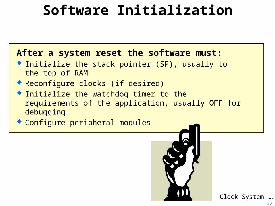
Software Initialization
After a system reset the software must: Initialize the stack pointer (SP), usually to the top of RAM Reconfigure clocks (if desired) Initialize the watchdog timer to the requirements of the
application, usually OFF for debugging Configure peripheral modules
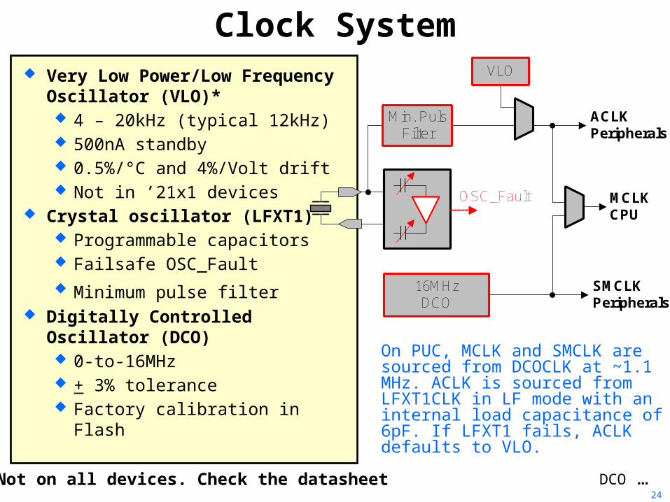
Clock System …23
MCLKCPU
SMCLKPeripherals
ACLKPeripherals
16MHzDCO
Min. Puls Filter
VLO
OSC_Fault
Clock System Very Low Power/Low Frequency
Oscillator (VLO)* 4 – 20kHz (typical 12kHz) 500nA standby 0.5%/°C and 4%/Volt drift Not in ’21x1 devices
Crystal oscillator (LFXT1) Programmable capacitors Failsafe OSC_Fault Minimum pulse filter
Digitally Controlled Oscillator (DCO) 0-to-16MHz + 3% tolerance Factory calibration in Flash
DCO …
On PUC, MCLK and SMCLK are sourced from DCOCLK at ~1.1 MHz. ACLK is sourced from LFXT1CLK in LF mode with an internal load capacitance of 6pF. If LFXT1 fails, ACLK defaults to VLO.
* Not on all devices. Check the datasheet24
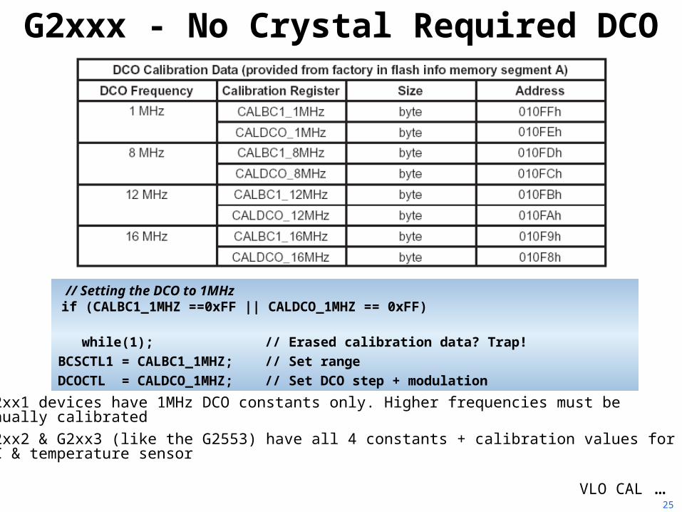
G2xxx - No Crystal Required DCO
// Setting the DCO to 1MHz if (CALBC1_1MHZ ==0xFF || CALDCO_1MHZ == 0xFF) while(1); // Erased calibration data? Trap!BCSCTL1 = CALBC1_1MHZ; // Set range DCOCTL = CALDCO_1MHZ; // Set DCO step + modulation
VLO CAL …
G2xx1 devices have 1MHz DCO constants only. Higher frequencies must be manually calibrated
G2xx2 & G2xx3 (like the G2553) have all 4 constants + calibration values for the ADC & temperature sensor
25
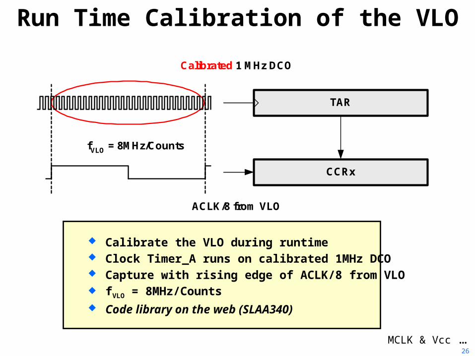
Run Time Calibration of the VLO
Calibrate the VLO during runtime Clock Timer_A runs on calibrated 1MHz DCO Capture with rising edge of ACLK/8 from VLO fVLO = 8MHz/Counts Code library on the web (SLAA340)
TAR
Calibrated 1 MHz DCO
CCRx
ACLK/8 from VLO
fVLO = 8MHz/Counts
MCLK & Vcc …26
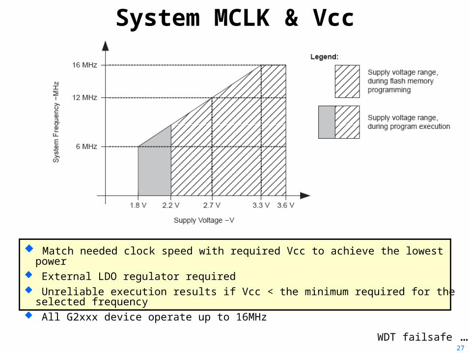
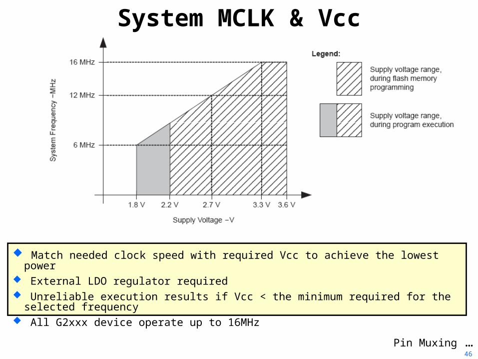
System MCLK & Vcc
WDT failsafe …
Match needed clock speed with required Vcc to achieve the lowest power External LDO regulator required Unreliable execution results if Vcc < the minimum required for the selected frequency All G2xxx device operate up to 16MHz
27
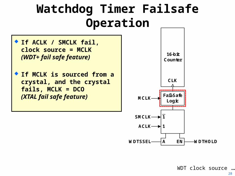
Watchdog Timer Failsafe Operation
If ACLK / SMCLK fail, clock source = MCLK(WDT+ fail safe feature)
If MCLK is sourced from a crystal, and the crystal fails, MCLK = DCO(XTAL fail safe feature)
Fail-Safe Logic
16-bitCounter
A EN
SMCLK
ACLK
MCLK
1
1
CLK
WDTSSEL WDTHOLD
WDT clock source …28
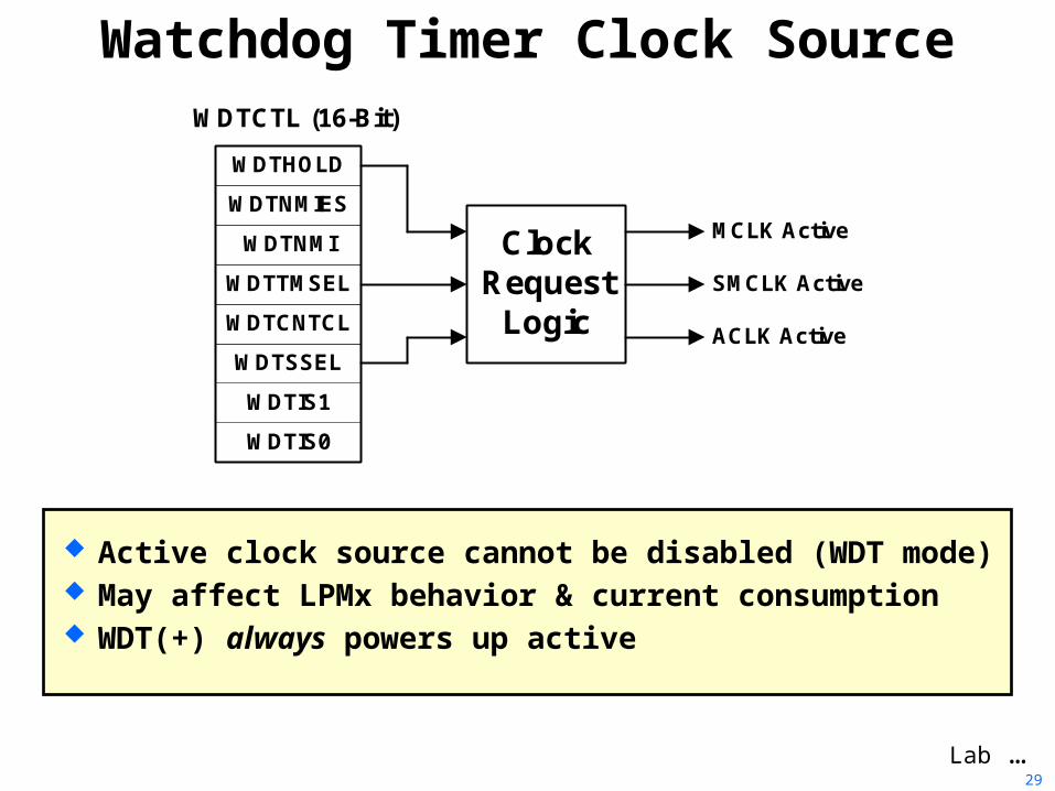
Watchdog Timer Clock Source
Active clock source cannot be disabled (WDT mode) May affect LPMx behavior & current consumption WDT(+) always powers up active
ClockRequest
LogicSMCLK Active
MCLK Active
ACLK Active
WDTIS0
WDTIS1
WDTSSEL
WDTCNTCL
WDTTMSEL
WDTNMI
WDTNMIES
WDTHOLD
WDTCTL (16-Bit)
Lab …29
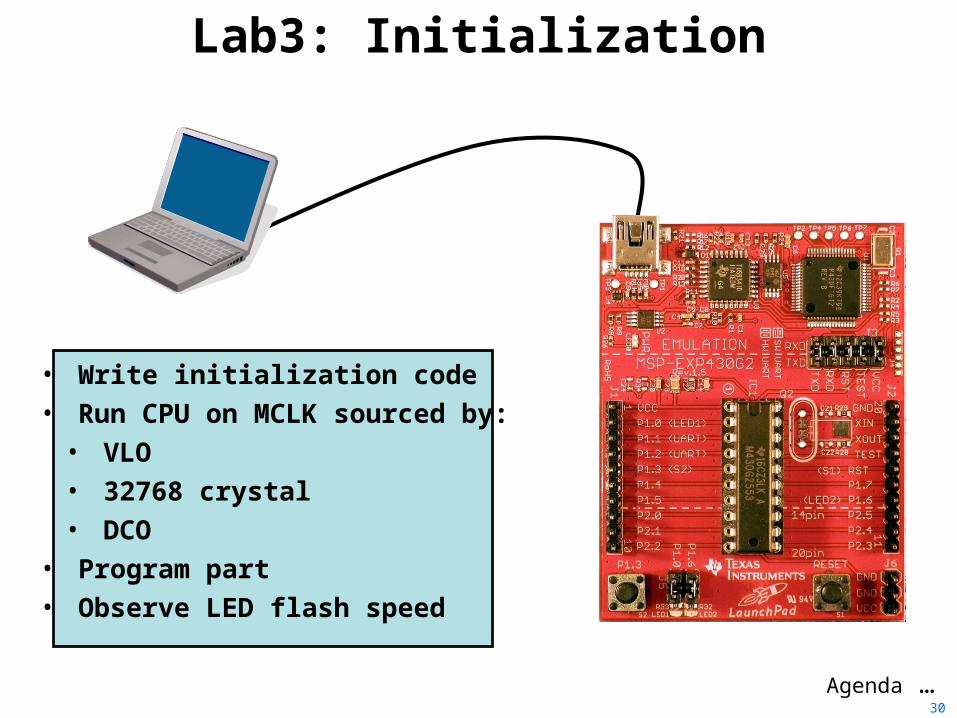
Lab3: Initialization
Agenda …
• Write initialization code• Run CPU on MCLK sourced by:
• VLO• 32768 crystal • DCO
• Program part • Observe LED flash speed
30

Agenda
ADC10 …
Introduction to Value LineCode Composer StudioInitialization and GPIO
Analog-to-Digital ConverterInterrupts and the TimerLow-Power OptimizationSerial Communications
GraceFRAM
Optional: Capacitive Touch
31
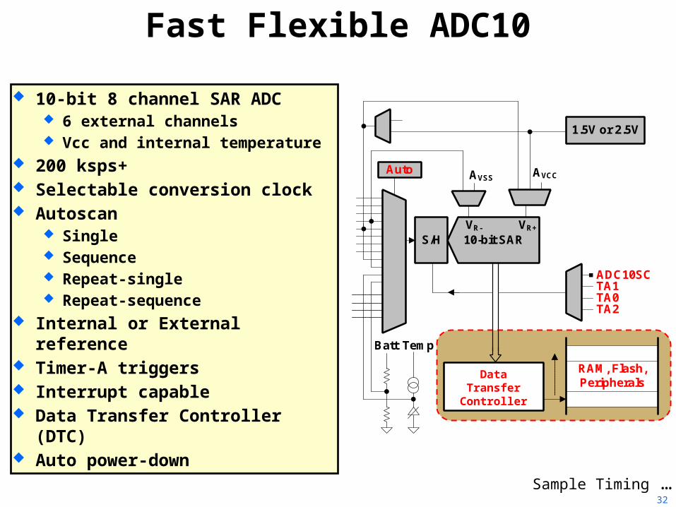
Fast Flexible ADC10
10-bit 8 channel SAR ADC 6 external channels Vcc and internal temperature
200 ksps+ Selectable conversion clock Autoscan
Single Sequence Repeat-single Repeat-sequence
Internal or External reference Timer-A triggers Interrupt capable Data Transfer Controller (DTC) Auto power-down
RAM, Flash, Peripherals
S/H 10-bit SAR
ADC10SCTA1
TA2TA0
Direct Transfer
Controller
VR- VR+
AVCCAVSS
1.5V or 2.5V
Auto
Batt Temp
DirectTransfer
Controller
DataTransfer
Controller
Sample Timing …32

Sample Timing
Reference must settle for <30uS Selectable hold time 13 clock conversion process Selectable clock source
- ADC10OSC (~5MHz)- ACLK- MCLK- SMCLK
Autoscan and DTC …33
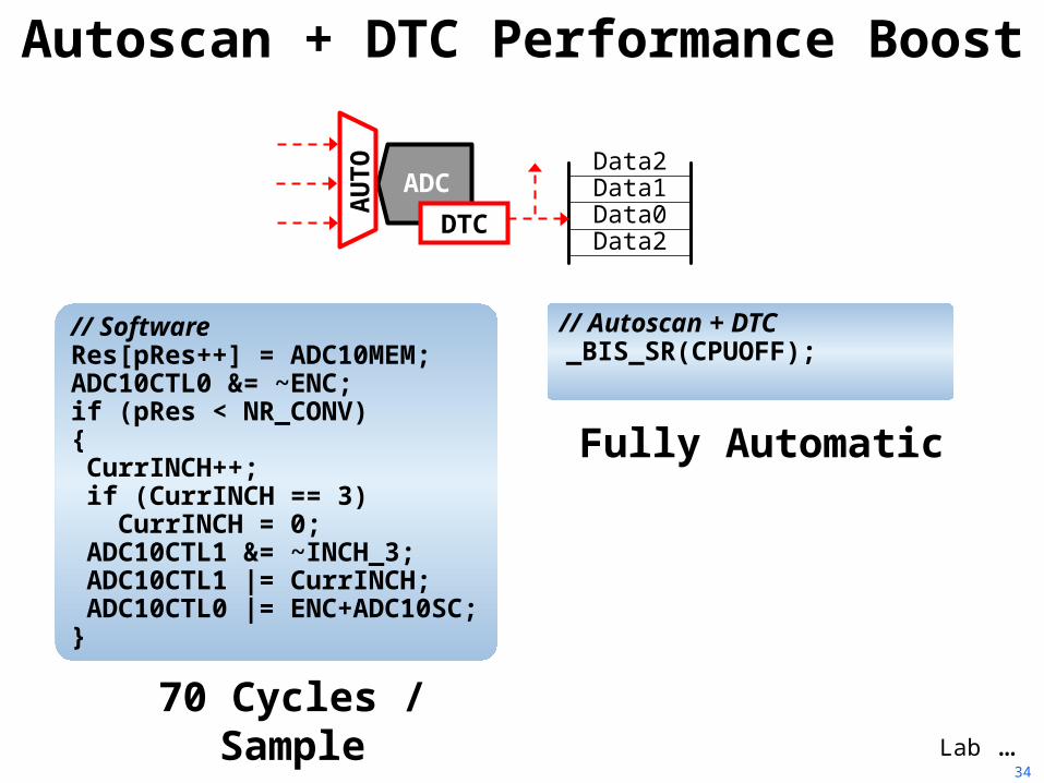
70 Cycles / Sample
Fully Automatic
Autoscan + DTC Performance Boost
Data2Data1Data0Data2
ADCDTCA
UTO
// Autoscan + DTC _BIS_SR(CPUOFF);
// Software Res[pRes++] = ADC10MEM;ADC10CTL0 &= ~ENC; if (pRes < NR_CONV) { CurrINCH++; if (CurrINCH == 3) CurrINCH = 0; ADC10CTL1 &= ~INCH_3; ADC10CTL1 |= CurrINCH; ADC10CTL0 |= ENC+ADC10SC;}
Lab …34
Lab4: ADC
Agenda …
• Measure internal temperature• Set timing requirements• Additional CCS features
35

Agenda
Timer Architecture …
Introduction to Value LineCode Composer StudioInitialization and GPIO
Analog-to-Digital ConverterInterrupts and the TimerLow-Power OptimizationSerial Communications
GraceFRAM
Optional: Capacitive Touch
36
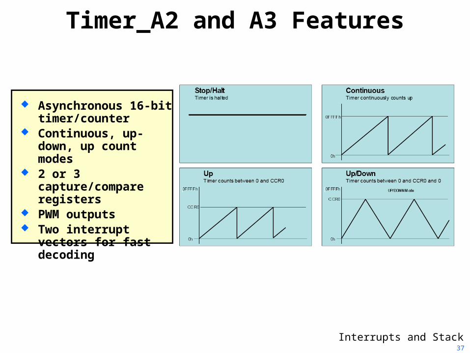
Timer_A2 and A3 Features
Asynchronous 16-bit timer/counter
Continuous, up-down, up count modes
2 or 3 capture/compare registers
PWM outputs Two interrupt vectors
for fast decoding
Interrupts and Stack …37

Interrupts and the StackEntering Interrupts
Any currently executing instruction is completed The PC, which points to the next instruction, is pushed onto the stack The SR is pushed onto the stack The interrupt with the highest priority is selected The interrupt request flag resets automatically on single-source flags; Multiple
source flags remain set for servicing by software The SR is cleared; This terminates any low-power mode; Because the GIE bit
is cleared, further interrupts are disabled The content of the interrupt vector is loaded into the PC; the program
continues with the interrupt service routine at that address
Vector Table …38
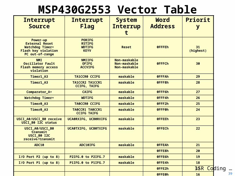
MSP430G2553 Vector TableInterrupt Source Interrupt Flag System
InterruptWord
AddressPriority
Power-upExternal Reset
Watchdog Timer+Flash key violation
PC out-of-range
PORIFGRSTIFGWDTIFG
KEYVReset 0FFFEh 31
(highest)
NMIOscillator Fault
Flash memory access violation
NMIIFGOFIFG
ACCVIFG
Non-maskableNon-maskableNon-maskable
0FFFCh 30
Timer1_A3 TA1CCR0 CCIFG maskable 0FFFAh 29Timer1_A3 TA1CCR2 TA1CCR1
CCIFG, TAIFGmaskable 0FFF8h 28
Comparator_A+ CAIFG maskable 0FFF6h 27Watchdog Timer+ WDTIFG maskable 0FFF4h 26
Timer0_A3 TA0CCR0 CCIFG maskable 0FFF2h 25Timer0_A3 TA0CCR1 TA0CCR1
CCIFG TAIFGmaskable 0FFF0h 24
USCI_A0/USCI_B0 receiveUSCI_B0 I2C status
UCA0RXIFG, UCB0RXIFG maskable 0FFEEh 23
USCI_A0/USCI_B0 transmitUSCI_B0 I2C receive/transmit
UCA0TXIFG, UCB0TXIFG maskable 0FFECh 22
ADC10 ADC10IFG maskable 0FFEAh 210FFE8h 20
I/O Port P2 (up to 8) P2IFG.0 to P2IFG.7 maskable 0FFE6h 19I/O Port P1 (up to 8) P1IFG.0 to P1IFG.7 maskable 0FFE4h 18
0FFE2h 17
0FFE0h 16
Boot Strap Loader Security Key
0FFDEh 15
Unused 0FFDEh to 0FFCDh 14 - 0
ISR Coding …39
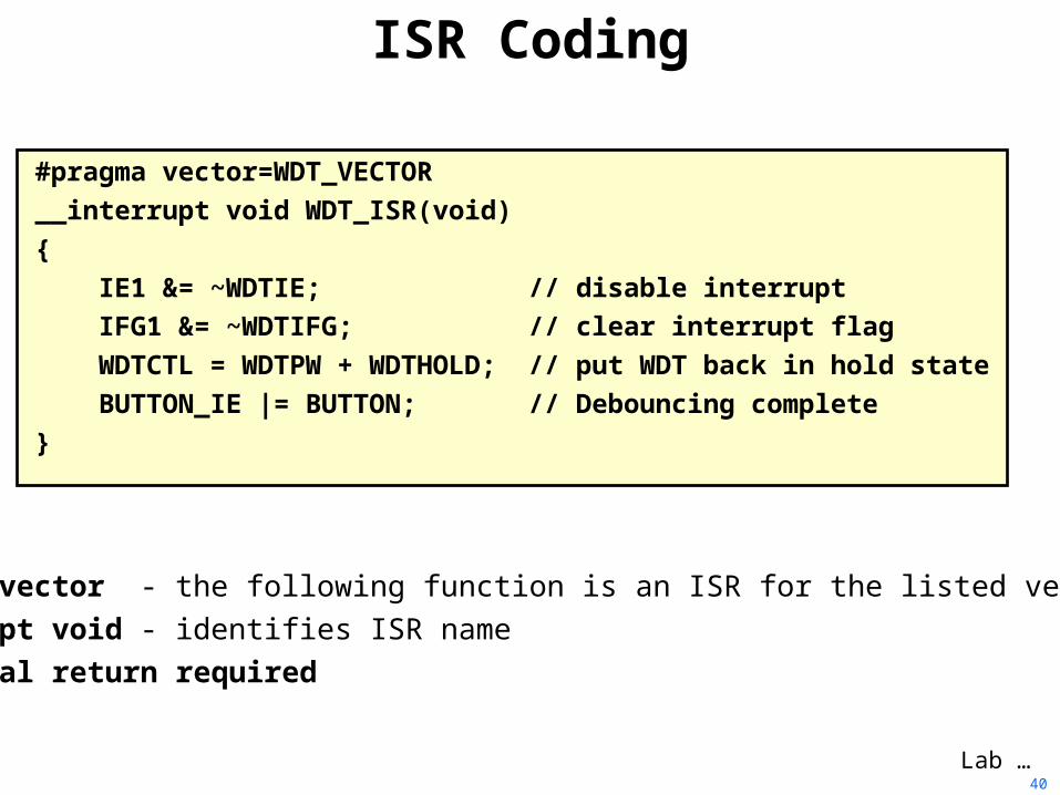
ISR Coding
#pragma vector=WDT_VECTOR__interrupt void WDT_ISR(void){ IE1 &= ~WDTIE; // disable interrupt IFG1 &= ~WDTIFG; // clear interrupt flag WDTCTL = WDTPW + WDTHOLD; // put WDT back in hold state BUTTON_IE |= BUTTON; // Debouncing complete}
#pragma vector - the following function is an ISR for the listed vector_interrupt void - identifies ISR nameNo special return required
Lab …40
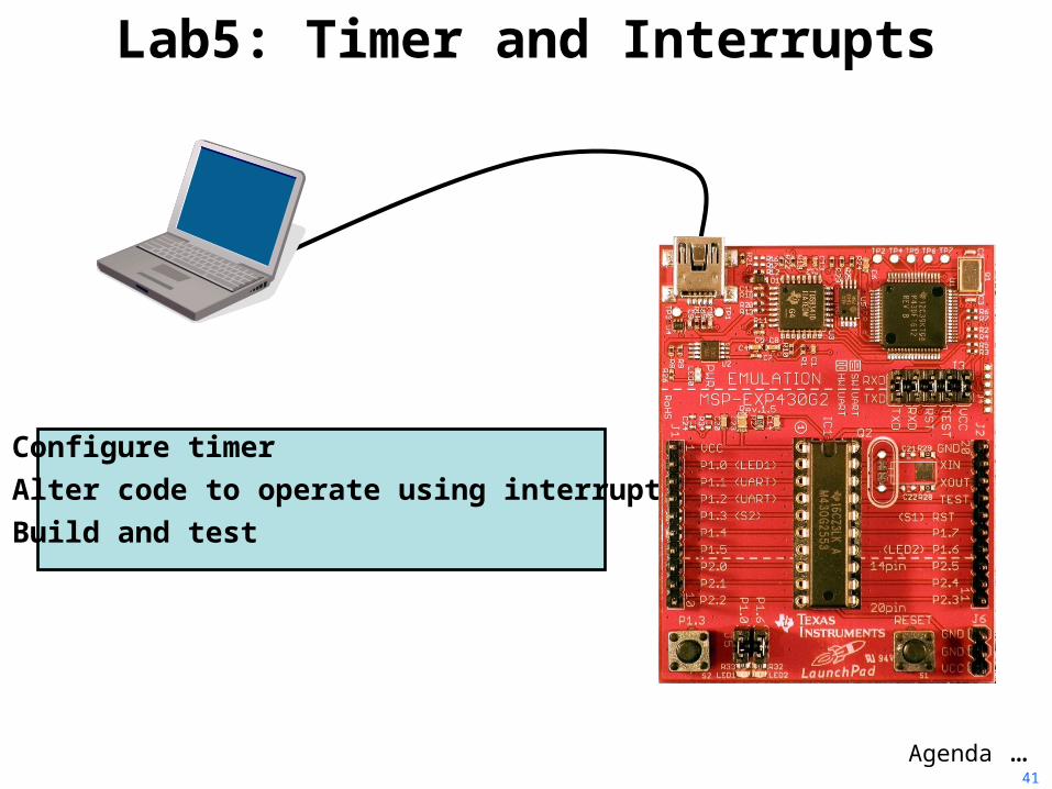
Lab5: Timer and Interrupts
Agenda …
• Configure timer• Alter code to operate using interrupts• Build and test
41
Agenda
Low Power Modes …
Introduction to Value LineCode Composer StudioInitialization and GPIO
Analog-to-Digital ConverterInterrupts and the TimerLow-Power OptimizationSerial Communications
GraceFRAM
Optional: Capacitive Touch
42
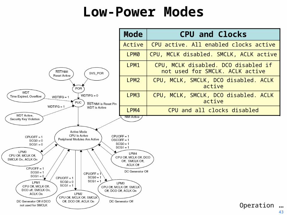
Low-Power ModesMode CPU and ClocksActive CPU active. All enabled clocks active
LPM0 CPU, MCLK disabled. SMCLK, ACLK active
LPM1 CPU, MCLK disabled. DCO disabled if not used for SMCLK. ACLK active
LPM2 CPU, MCLK, SMCLK, DCO disabled. ACLK active
LPM3 CPU, MCLK, SMCLK, DCO disabled. ACLK active
LPM4 CPU and all clocks disabled
Operation …43
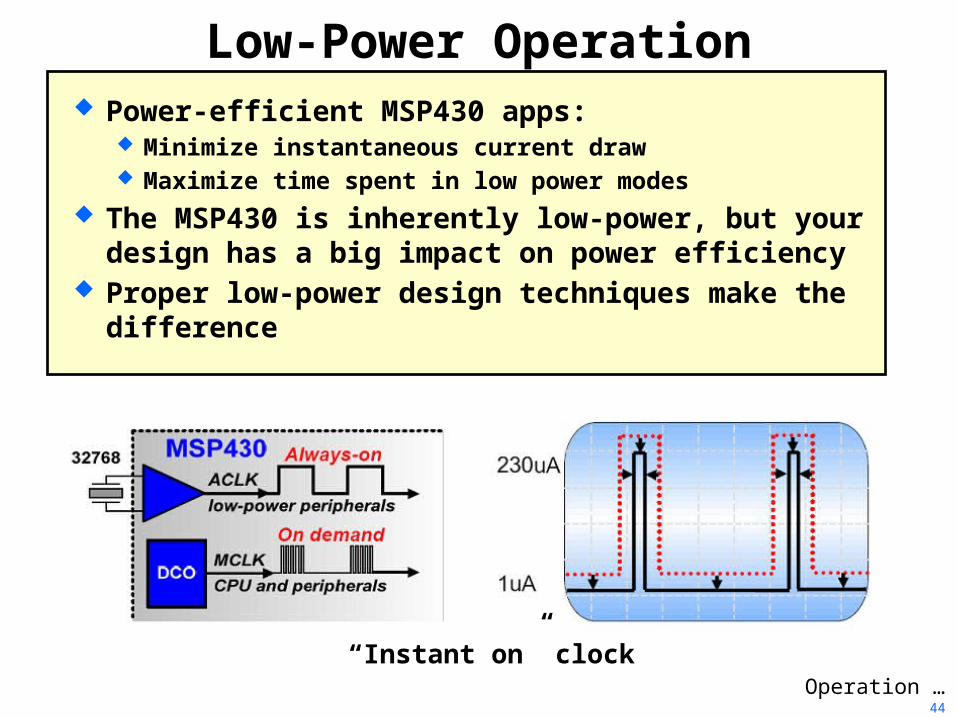
Low-Power Operation Power-efficient MSP430 apps:
Minimize instantaneous current draw Maximize time spent in low power modes
The MSP430 is inherently low-power, but your design has a big impact on power efficiency
Proper low-power design techniques make the difference
Operation …“Instant on” clock
44
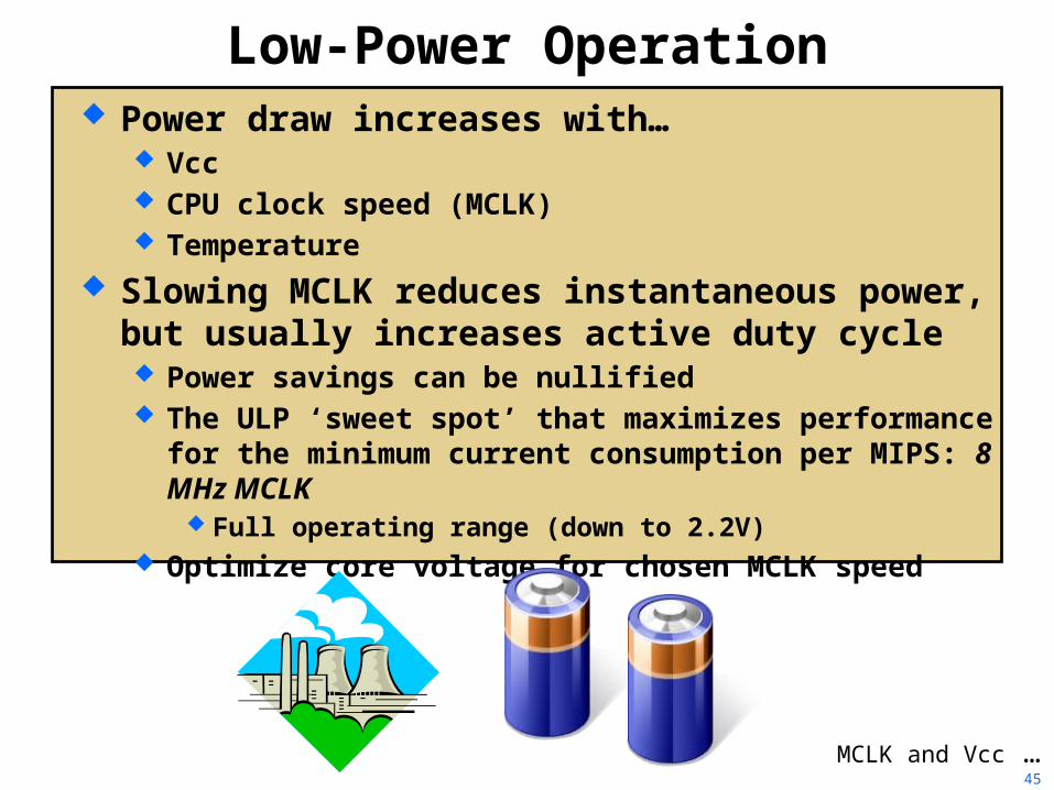
Low-Power Operation Power draw increases with…
Vcc CPU clock speed (MCLK) Temperature
Slowing MCLK reduces instantaneous power, but usually increases active duty cycle Power savings can be nullified The ULP ‘sweet spot’ that maximizes performance for the
minimum current consumption per MIPS: 8 MHz MCLK Full operating range (down to 2.2V)
Optimize core voltage for chosen MCLK speed
MCLK and Vcc …45
System MCLK & Vcc
Pin Muxing …
Match needed clock speed with required Vcc to achieve the lowest power External LDO regulator required Unreliable execution results if Vcc < the minimum required for the selected frequency All G2xxx device operate up to 16MHz
46
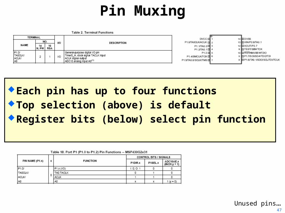
Pin Muxing
Each pin has up to four functionsTop selection (above) is defaultRegister bits (below) select pin function
Unused pins…47
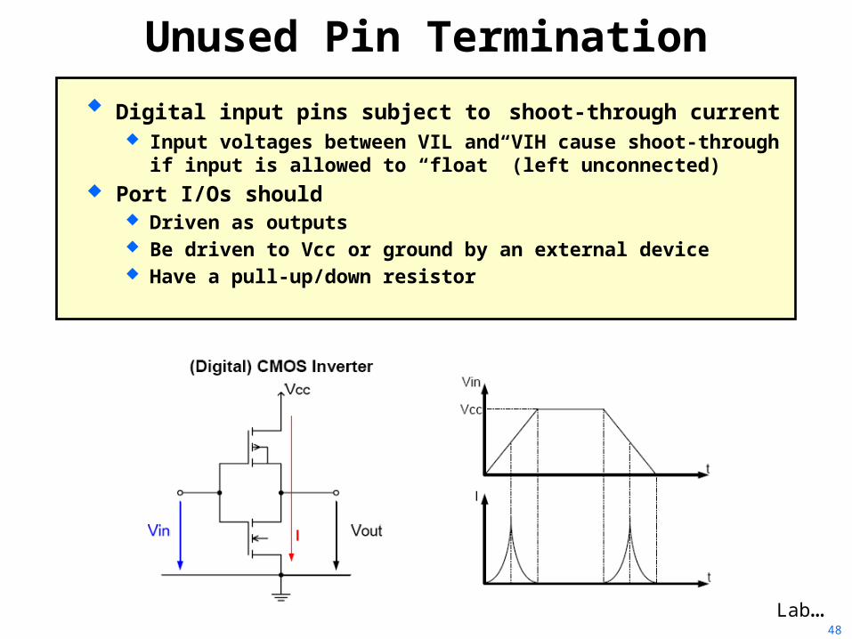
Unused Pin Termination Digital input pins subject to shoot-through current
Input voltages between VIL and VIH cause shoot-through if input is allowed to “float” (left unconnected)
Port I/Os should Driven as outputs Be driven to Vcc or ground by an external device Have a pull-up/down resistor
Lab…48
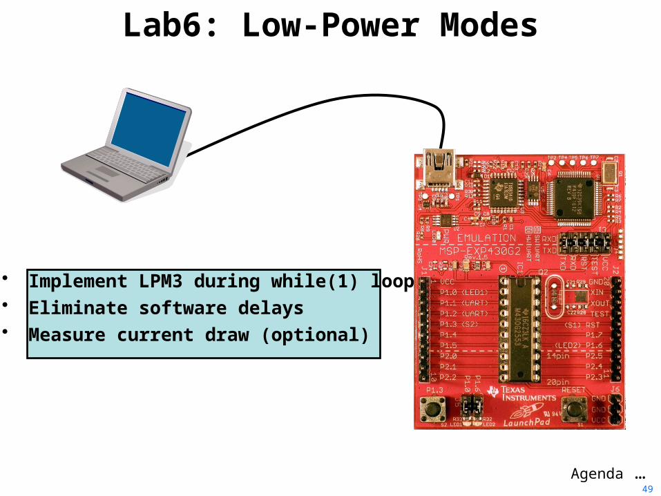
Lab6: Low-Power Modes
Agenda …
• Implement LPM3 during while(1) loop• Eliminate software delays• Measure current draw (optional)
49
Agenda
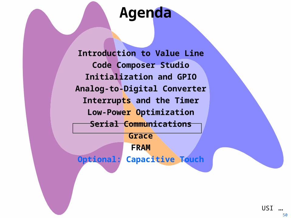
USI …
Introduction to Value LineCode Composer StudioInitialization and GPIO
Analog-to-Digital ConverterInterrupts and the TimerLow-Power OptimizationSerial Communications
GraceFRAM
Optional: Capacitive Touch
50
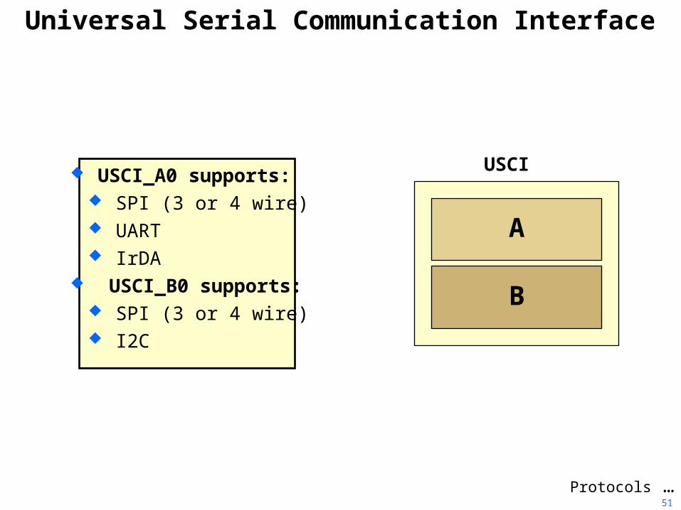
Universal Serial Communication Interface
USCI_A0 supports: SPI (3 or 4 wire) UART IrDA
USCI_B0 supports: SPI (3 or 4 wire) I2C
Protocols …
USCI
A
B
51
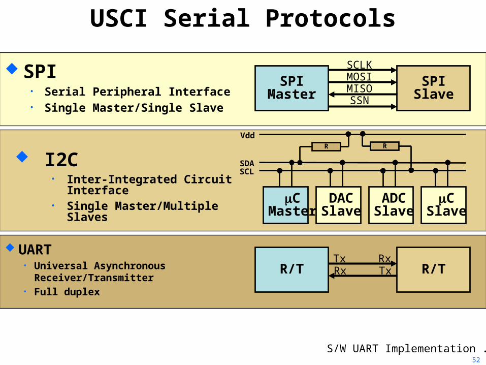
USCI Serial Protocols
SPI• Serial Peripheral Interface• Single Master/Single Slave
SPIMaster
SPISlave
SCLKMOSIMISOSSN
I2C• Inter-Integrated Circuit Interface• Single Master/Multiple Slaves C
MasterDACSlave
ADCSlave
CSlave
RR
SCLSDA
Vdd
S/W UART Implementation …
UART• Universal Asynchronous
Receiver/Transmitter• Full duplex
R/T R/TTxRx
RxTx
52
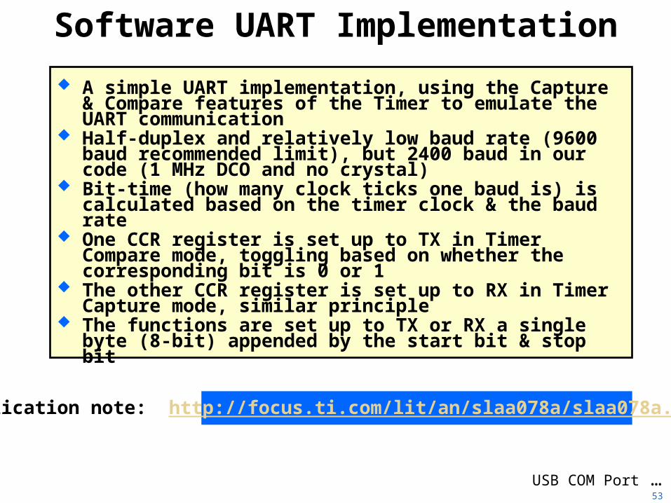
Software UART Implementation A simple UART implementation, using the Capture &
Compare features of the Timer to emulate the UART communication
Half-duplex and relatively low baud rate (9600 baud recommended limit), but 2400 baud in our code (1 MHz DCO and no crystal)
Bit-time (how many clock ticks one baud is) is calculated based on the timer clock & the baud rate
One CCR register is set up to TX in Timer Compare mode, toggling based on whether the corresponding bit is 0 or 1
The other CCR register is set up to RX in Timer Capture mode, similar principle
The functions are set up to TX or RX a single byte (8-bit) appended by the start bit & stop bit
Application note: http://focus.ti.com/lit/an/slaa078a/slaa078a.pdf
USB COM Port …53
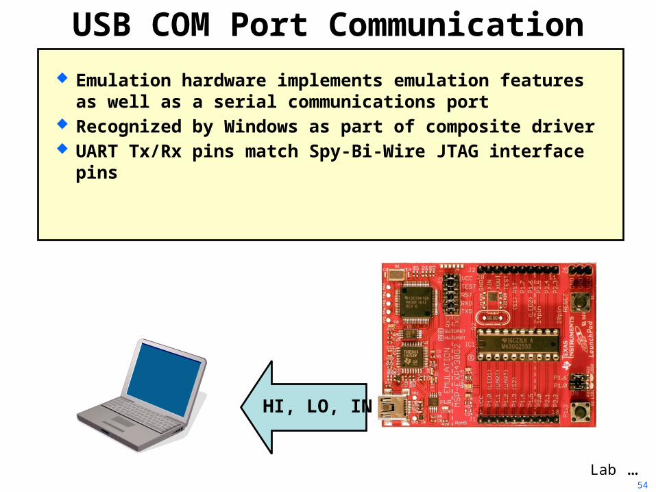
USB COM Port Communication Emulation hardware implements emulation features
as well as a serial communications port Recognized by Windows as part of composite driver UART Tx/Rx pins match Spy-Bi-Wire JTAG interface
pins
Lab …
HI, LO, IN
54
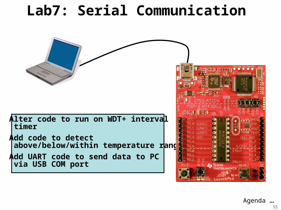
Lab7: Serial Communication
• Alter code to run on WDT+ interval timer
• Add code to detect above/below/within temperature range
• Add UART code to send data to PC via USB COM port
Agenda …55

Agenda
What is Grace?
Introduction to Value LineCode Composer StudioInitialization and GPIO
Analog-to-Digital ConverterInterrupts and the TimerLow-Power OptimizationSerial Communications
GraceFRAM
Optional: Capacitive Touch
56
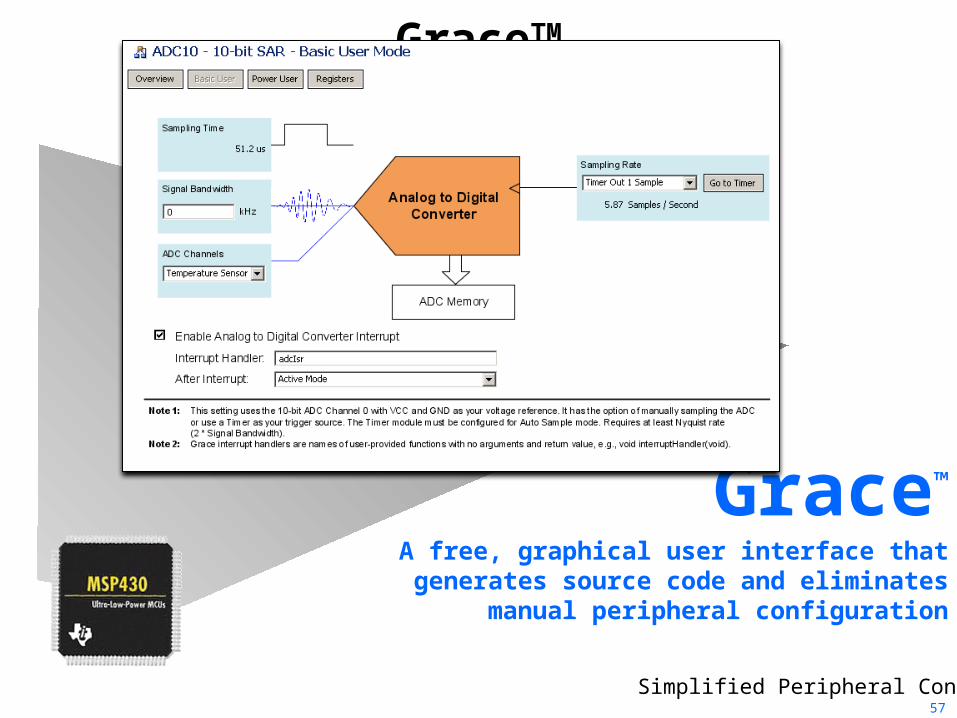
GraceTM
Grace™
A free, graphical user interface that generates source code and eliminates manual peripheral
configuration
Simplified Peripheral Config57
Simplified Peripheral Configuration
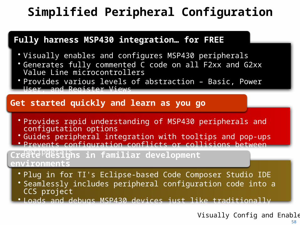
Fully harness MSP430 integration… for FREE
Create designs in familiar development environments
• Visually enables and configures MSP430 peripherals• Generates fully commented C code on all F2xx and G2xx Value Line
microcontrollers• Provides various levels of abstraction – Basic, Power User, and Register Views
• Provides rapid understanding of MSP430 peripherals and configutation options• Guides peripheral integration with tooltips and pop-ups • Prevents configuration conflicts or collisions between peripherals
• Plug in for TI's Eclipse-based Code Composer Studio IDE• Seamlessly includes peripheral configuration code into a CCS project• Loads and debugs MSP430 devices just like traditionally generated code
Get started quickly and learn as you go
Visually Config and Enable …58
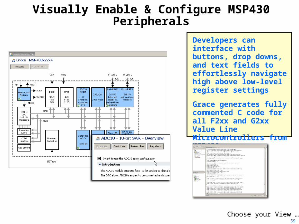
Visually Enable & Configure MSP430 Peripherals
Developers can interface with buttons, drop downs, and text fields to effortlessly navigate high above low-level register settings
Grace generates fully commented C code for all F2xx and G2xx Value Line Microcontrollers from MSP430
Choose your View …59
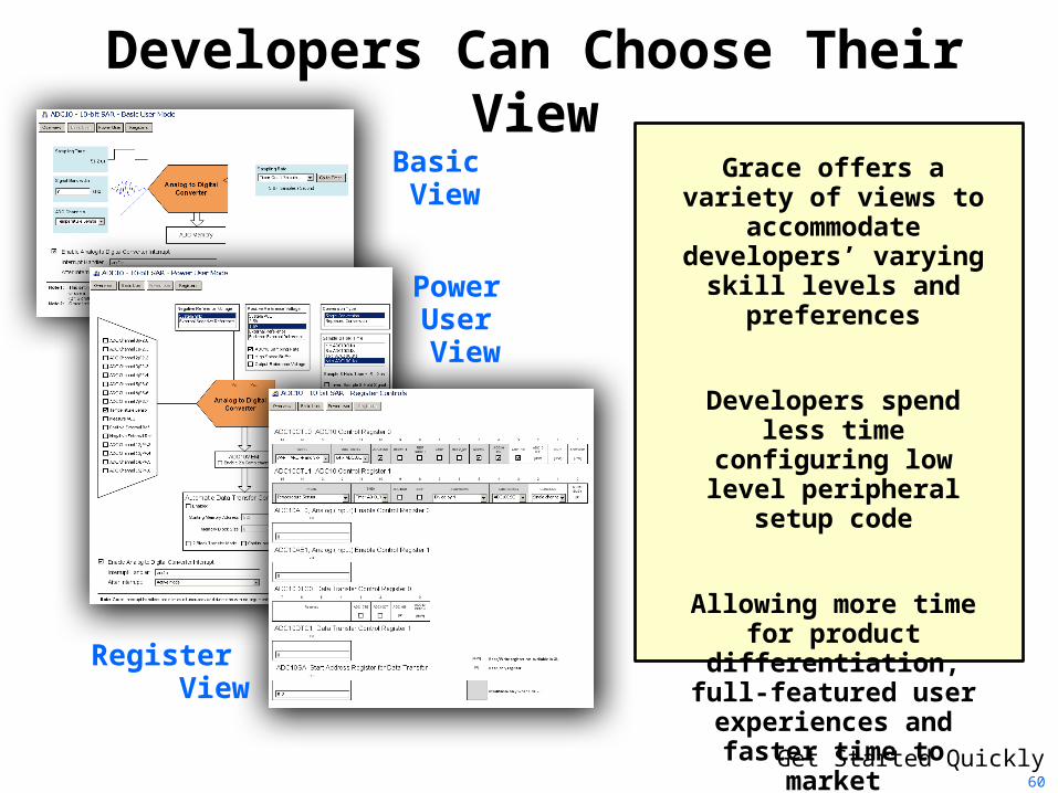
Developers Can Choose Their View
Basic View
Power User View
Register View
Grace offers a variety of views to accommodate
developers’ varying skill levels and preferences
Developers spend less time configuring low level
peripheral setup code
Allowing more time for product differentiation,
full-featured user experiences and faster
time to market
Get Started Quickly …60
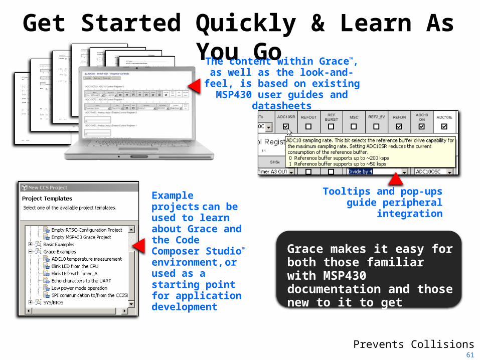
Get Started Quickly & Learn As You GoThe content within Grace™, as
well as the look-and-feel, is based on existing MSP430 user
guides and datasheets
Tooltips and pop-ups guide peripheral integration
Grace makes it easy for both those familiar with MSP430 documentation and those new to it to get started
Example projects
can be used to learn about Grace and the Code Composer Studio™ environment, ,, or used as a starting point for application development
Prevents Collisions …61
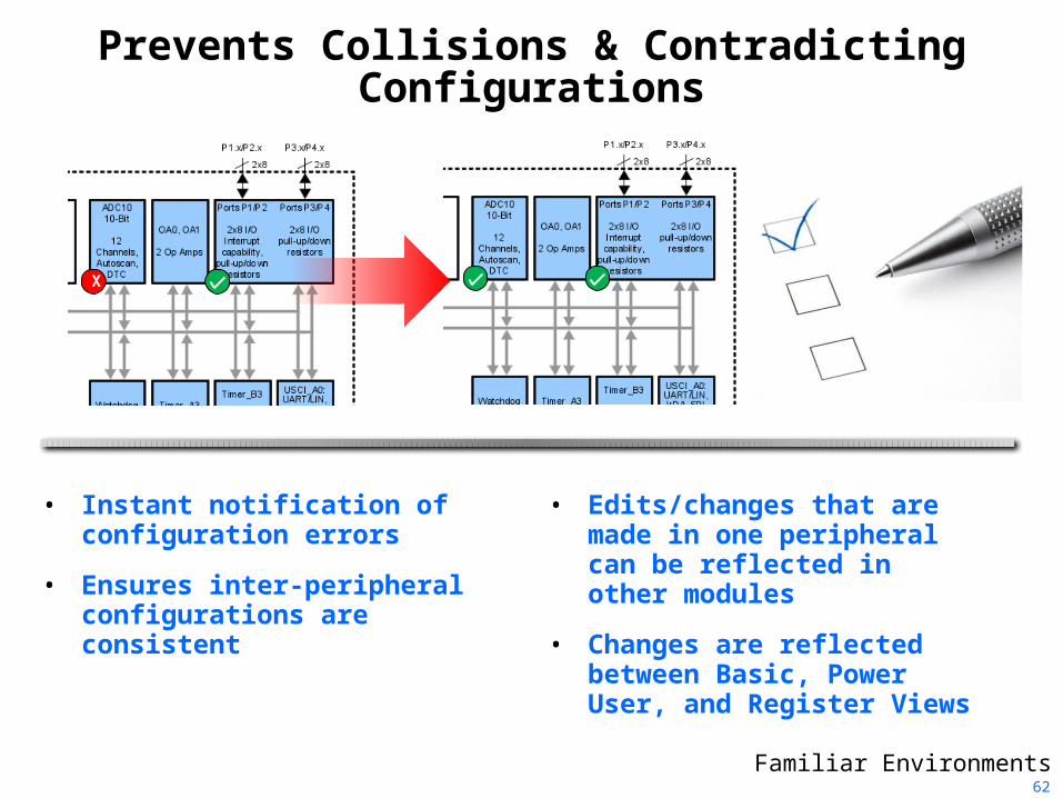
Prevents Collisions & Contradicting Configurations
• Instant notification of configuration errors
• Ensures inter-peripheral configurations are consistent
X
• Edits/changes that are made in one peripheral can be reflected in other modules
• Changes are reflected between Basic, Power User, and Register Views
Familiar Environments …62
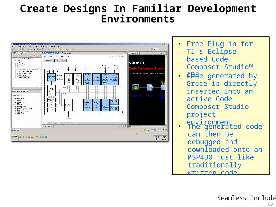
Create Designs In Familiar Development Environments
• The generated code can then be debugged and downloaded onto an MSP430 just like traditionally written code
• Free Plug in for TI's Eclipse-based Code Composer Studio™ IDE
• Code generated by Grace is directly inserted into an active Code Composer Studio project environment
Seamless Include63
Rita Sulma
should this be "environment"?
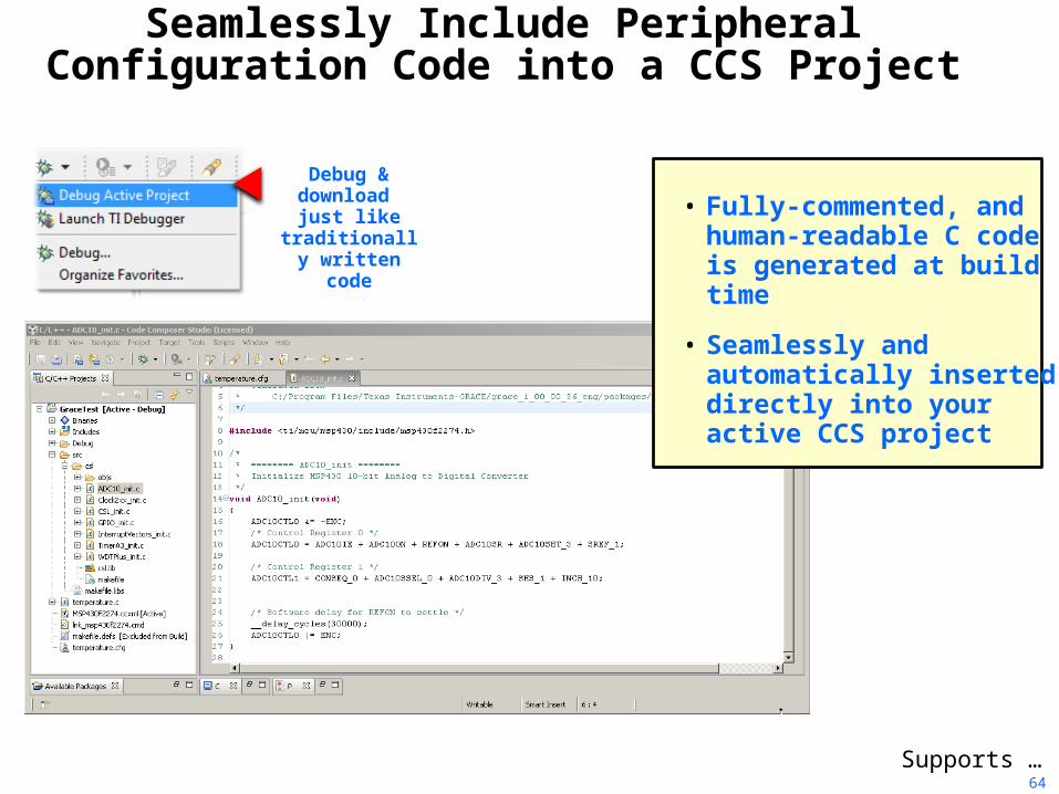
Seamlessly Include Peripheral Configuration Code into a CCS Project
• Fully-commented, and human-readable C code is generated at build time
• Seamlessly and automatically inserted directly into your active CCS project
Debug & download
just like traditionally written code
Supports …64
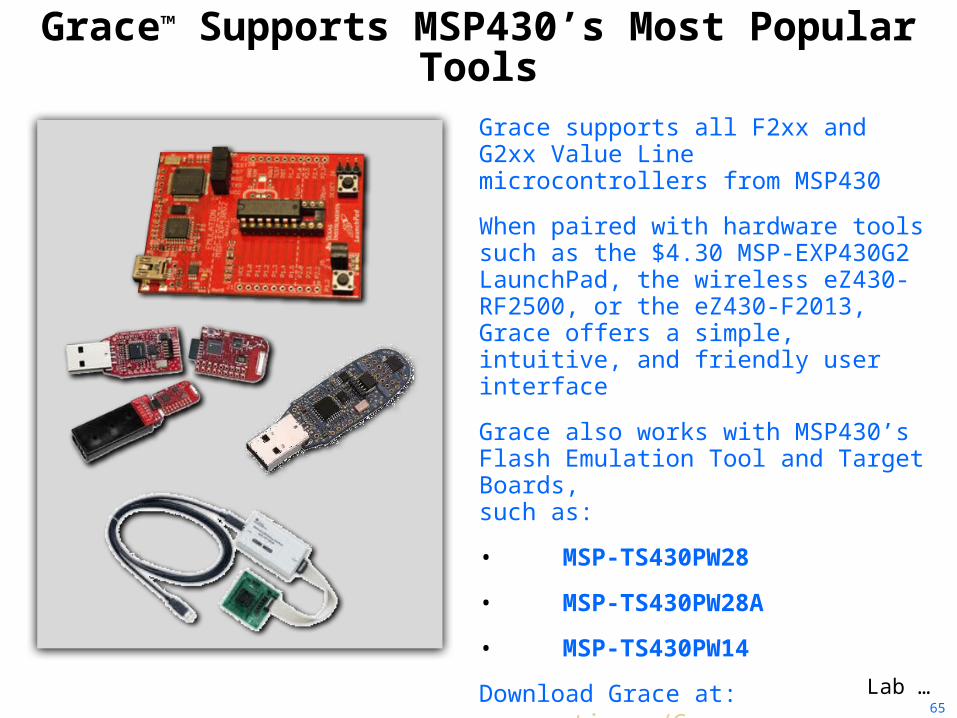
Grace™ Supports MSP430’s Most Popular Tools
Grace supports all F2xx and G2xx Value Line microcontrollers from MSP430
When paired with hardware tools such as the $4.30 MSP-EXP430G2 LaunchPad, the wireless eZ430-RF2500, or the eZ430-F2013, Grace offers a simple, intuitive, and friendly user interface
Grace also works with MSP430’s Flash Emulation Tool and Target Boards, such as:
• MSP-TS430PW28
• MSP-TS430PW28A
• MSP-TS430PW14
Download Grace at: www.ti.com/Grace
Lab …65
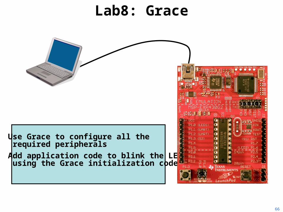
Lab8: Grace
• Use Grace to configure all the required peripherals
• Add application code to blink the LED using the Grace initialization code
66
Agenda
Introduction to Value LineCode Composer StudioInitialization and GPIO
Analog-to-Digital ConverterInterrupts and the TimerLow-Power OptimizationSerial Communications
GraceFRAM
Optional: Capacitive Touch
67
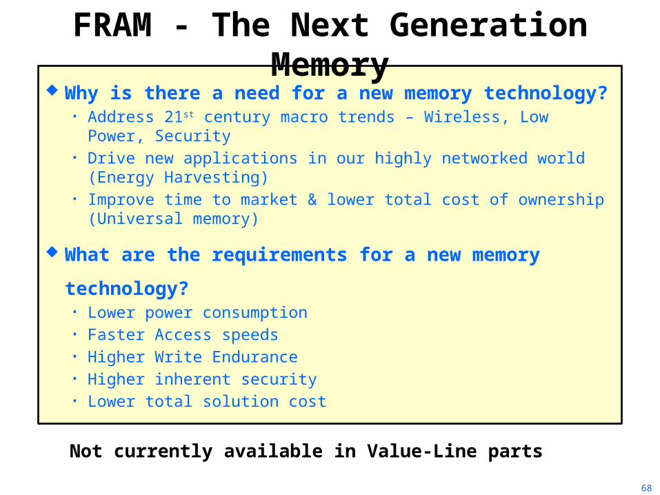
FRAM - The Next Generation Memory
Why is there a need for a new memory technology? • Address 21st century macro trends – Wireless, Low Power, Security• Drive new applications in our highly networked world (Energy
Harvesting)• Improve time to market & lower total cost of ownership (Universal
memory)
What are the requirements for a new memory
technology? • Lower power consumption• Faster Access speeds• Higher Write Endurance• Higher inherent security• Lower total solution cost
Not currently available in Value-Line parts
68
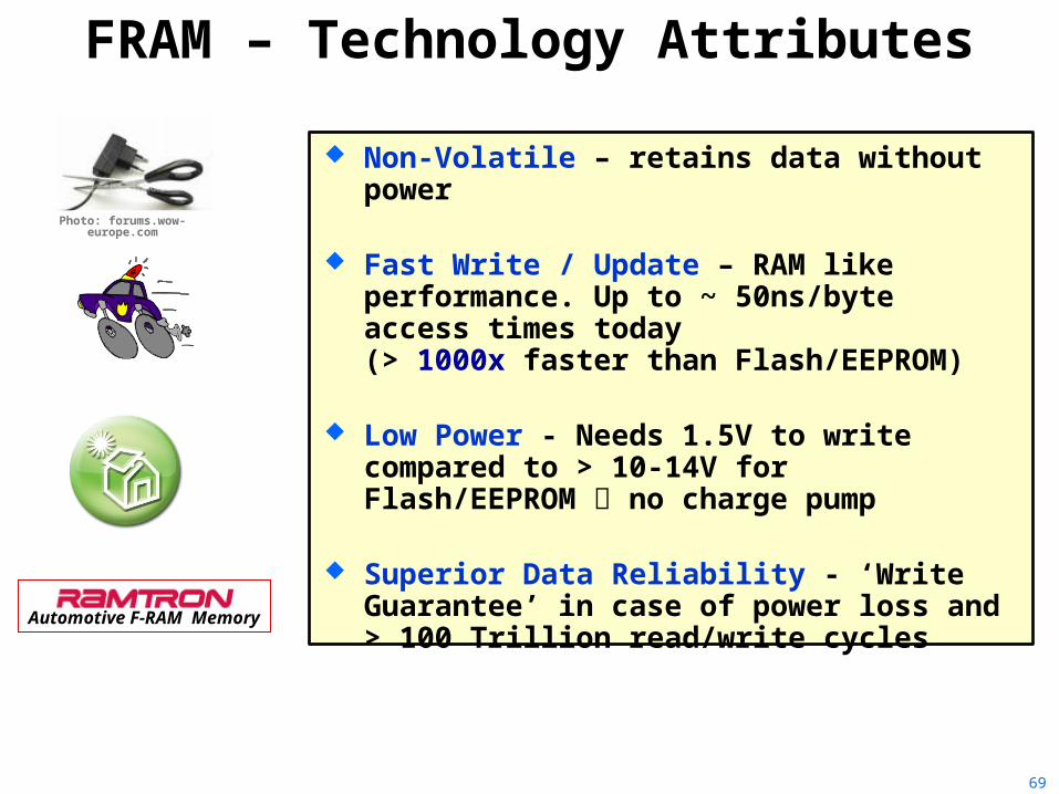
FRAM – Technology Attributes
Non-Volatile – retains data without power
Fast Write / Update – RAM like performance. Up to ~ 50ns/byte access times today (> 1000x faster than Flash/EEPROM)
Low Power - Needs 1.5V to write compared to > 10-14V for Flash/EEPROM no charge pump
Superior Data Reliability - ‘Write Guarantee’ in case of power loss and > 100 Trillion read/write cycles
Automotive F-RAM Memory
Photo: forums.wow-europe.com
69
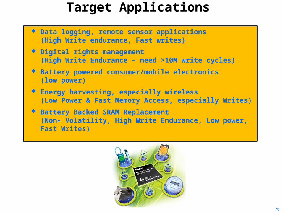
Data logging, remote sensor applications (High Write endurance, Fast writes)
Digital rights management (High Write Endurance – need >10M write cycles)
Battery powered consumer/mobile electronics (low power)
Energy harvesting, especially wireless (Low Power & Fast Memory Access, especially Writes)
Battery Backed SRAM Replacement (Non- Volatility, High Write Endurance, Low power, Fast Writes)
Target Applications
70
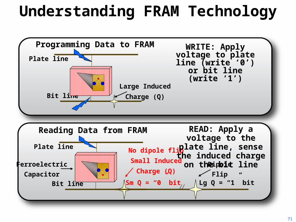
Understanding FRAM Technology
WRITE: Apply voltage to plate line (write ‘0’) or
bit line (write ‘1’)
Bit line
Plate line
Large InducedCharge (Q)
Programming Data to FRAM
Bit line
Plate line No dipole flipSmall Induced
Charge (Q)
Reading Data from FRAM
DipoleFlip
FerroelectricCapacitor
READ: Apply a voltage to the plate line, sense the induced
charge on the bit line
Sm Q = “0” bit Lg Q = “1” bit
71
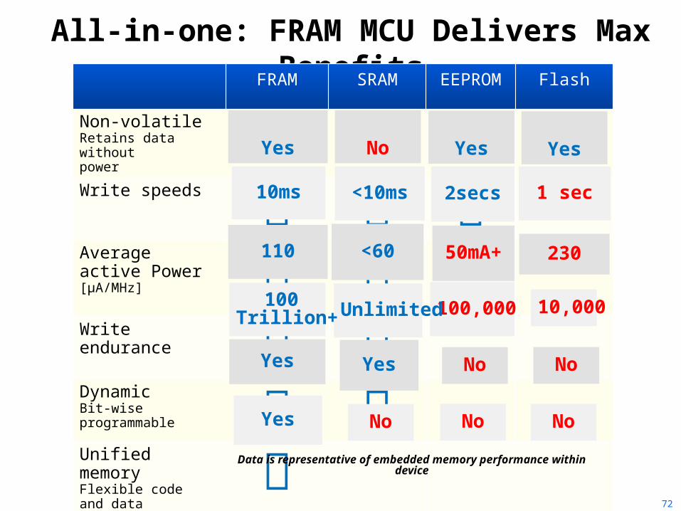
All-in-one: FRAM MCU Delivers Max BenefitsFRAM SRAM EEPROM Flash
Non-volatile Retains data without power Write speeds Average active Power [µA/MHz] Write endurance DynamicBit-wise programmable Unified memoryFlexible code and data partitioning
Yes Yes YesNo
10ms 2secs<10ms 1 sec
50mA+<60110 230
10,000100,000Unlimited100 Trillion+
YesYes NoNo
Yes NoNoNo
Data is representative of embedded memory performance within device
72
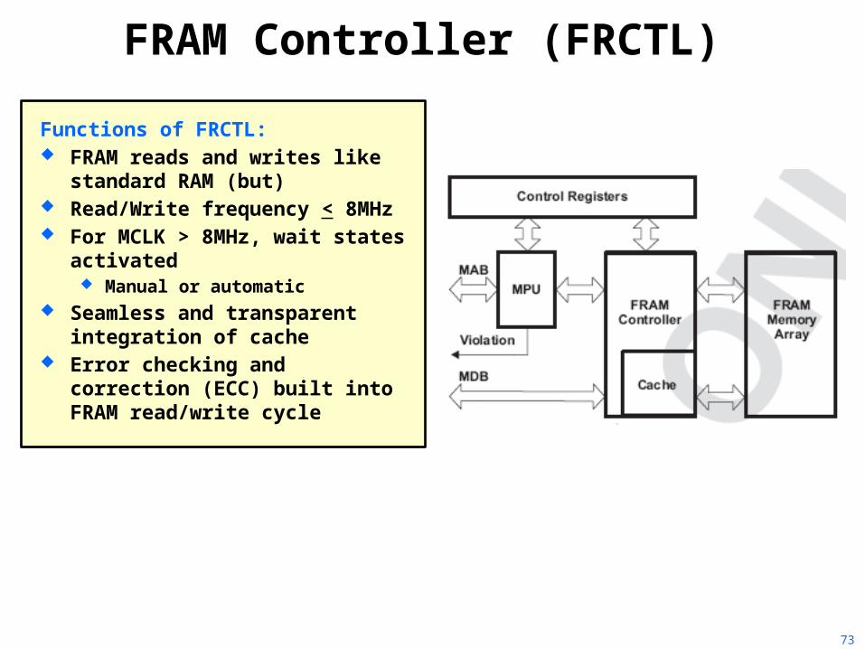
FRAM Controller (FRCTL)
Functions of FRCTL: FRAM reads and writes like
standard RAM (but) Read/Write frequency < 8MHz For MCLK > 8MHz, wait states
activated Manual or automatic
Seamless and transparent integration of cache
Error checking and correction (ECC) built into FRAM read/write cycle
73
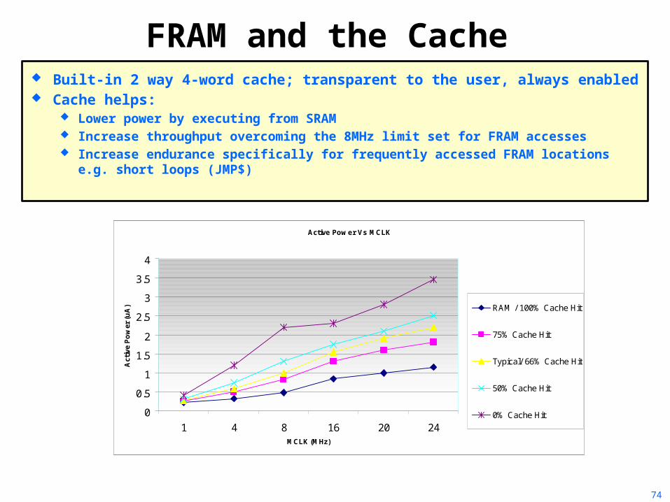
FRAM and the Cache Built-in 2 way 4-word cache; transparent to the user, always enabled Cache helps:
Lower power by executing from SRAM Increase throughput overcoming the 8MHz limit set for FRAM accesses Increase endurance specifically for frequently accessed FRAM locations e.g.
short loops (JMP$)
Active Pow er Vs MCLK
0
0.5
1
1.5
2
2.5
3
3.5
4
1 4 8 16 20 24MCLK (MHz)
Act
ive
Pow
er (u
A) RAM / 100% Cache Hit
75% Cache Hit
Typical/ 66% Cache Hit
50% Cache Hit
0% Cache Hit
74
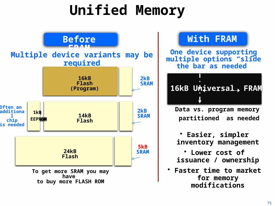
Unified Memory
One device supporting multiple options “slide the bar
as needed”Multiple device variants may be
required
• Easier, simpler inventory management
• Lower cost of issuance / ownership
• Faster time to market for memory modifications
Before FRAM With FRAM
To get more SRAM you may have to buy more FLASH ROM
1kB EEPROM
Often an additional
chipis needed
14kB Flash2kB
SRAM
16kB Flash (Program)
2kB SRAM
24kB Flash 5kB SRAM
16kB Universal FRAM
Data vs. program memory partitioned as needed
75
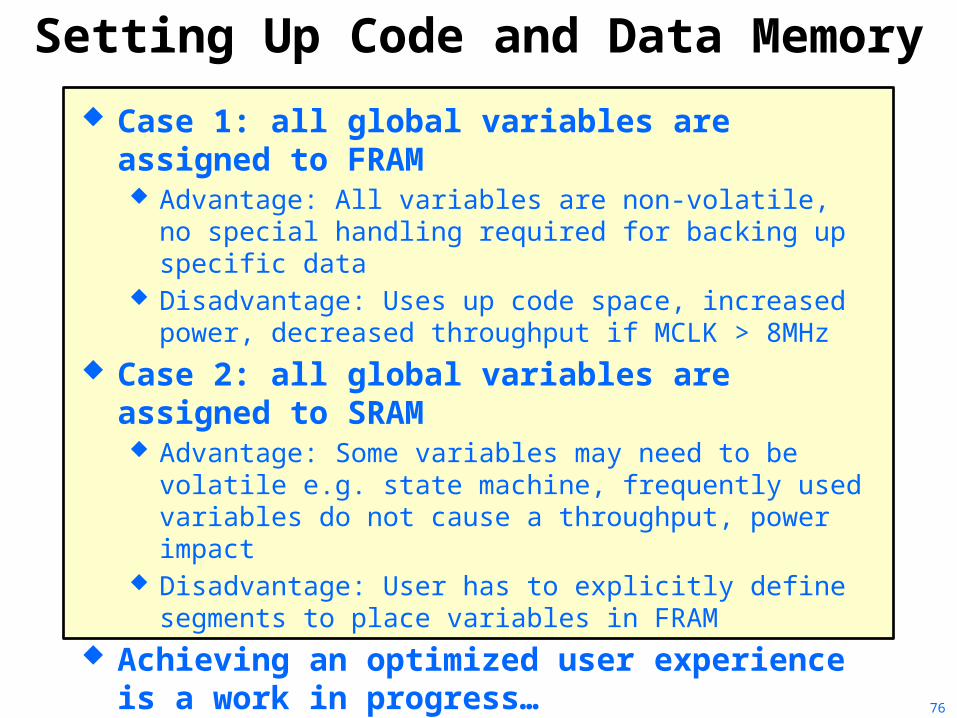
Setting Up Code and Data Memory Case 1: all global variables are assigned to FRAM
Advantage: All variables are non-volatile, no special handling required for backing up specific data
Disadvantage: Uses up code space, increased power, decreased throughput if MCLK > 8MHz
Case 2: all global variables are assigned to SRAM Advantage: Some variables may need to be volatile e.g.
state machine, frequently used variables do not cause a throughput, power impact
Disadvantage: User has to explicitly define segments to place variables in FRAM
Achieving an optimized user experience is a work in progress…
76
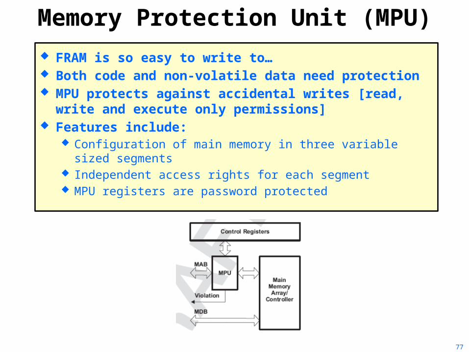
Memory Protection Unit (MPU) FRAM is so easy to write to… Both code and non-volatile data need protection MPU protects against accidental writes [read, write and
execute only permissions] Features include:
Configuration of main memory in three variable sized segments
Independent access rights for each segment MPU registers are password protected
77
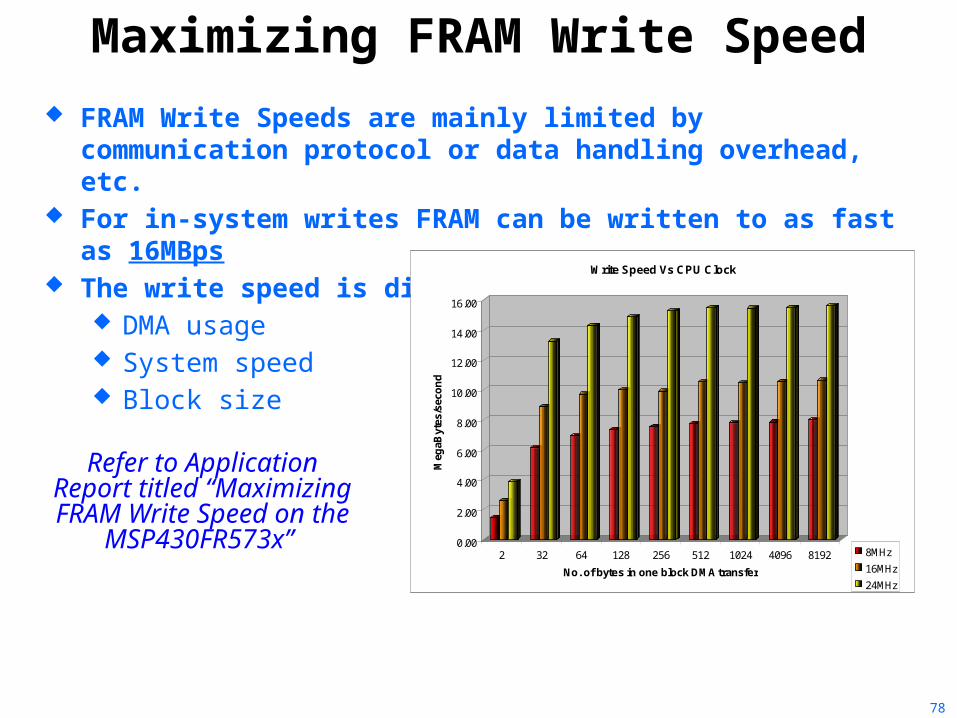
Maximizing FRAM Write Speed FRAM Write Speeds are mainly limited by communication
protocol or data handling overhead, etc. For in-system writes FRAM can be written to as fast as 16MBps The write speed is directly dependent on:
DMA usage System speed Block size
0.00
2.00
4.00
6.00
8.00
10.00
12.00
14.00
16.00
Meg
aByt
es/s
econ
d
2 32 64 128 256 512 1024 4096 8192
No. of bytes in one block DMA transfer
Write Speed Vs CPU Clock
8MHz16MHz24MHz
Refer to Application Report titled “Maximizing FRAM Write Speed on the MSP430FR573x”
78

• Case Example: MSP430FR5739 vs. MSP430F2274• Both devices use System clock = 8MHz• Maximum Speed FRAM = 1.4MBps [100x faster]• Maximum Speed Flash = 13kBps
FRAM = Ultra-Fast Writes
1,400kBps
13kBps
Max. Throughput:
79
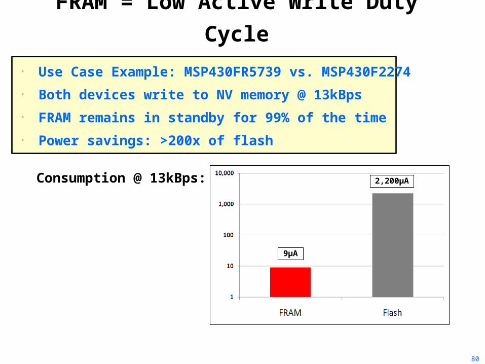
• Use Case Example: MSP430FR5739 vs. MSP430F2274• Both devices write to NV memory @ 13kBps• FRAM remains in standby for 99% of the time• Power savings: >200x of flash
FRAM = Low Active Write Duty Cycle
Consumption @ 13kBps:
9μA
2,200μA
80
81
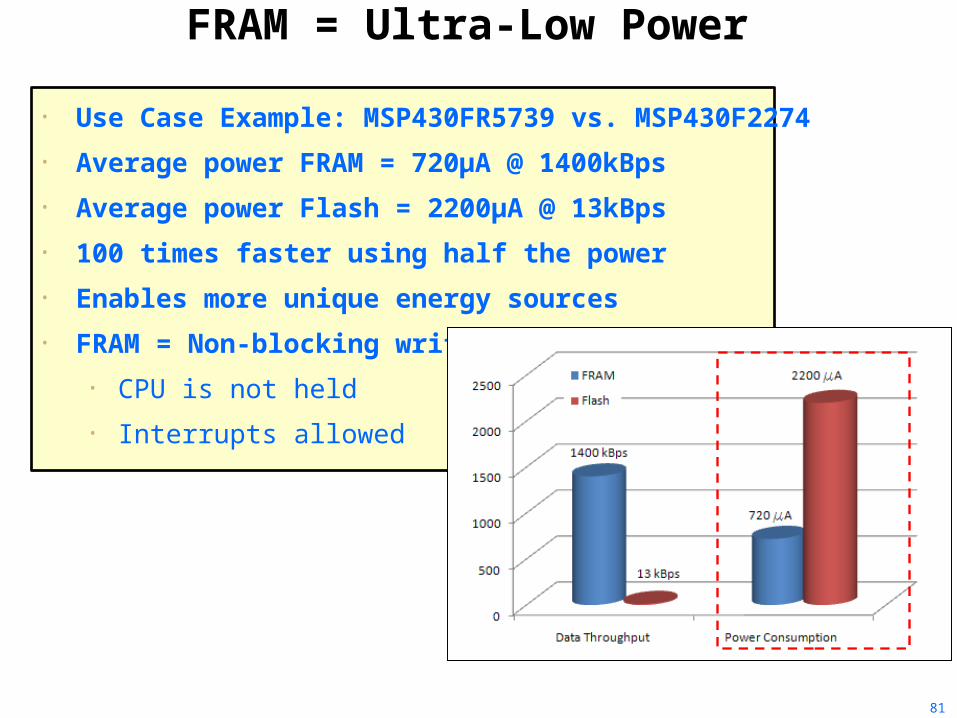
• Use Case Example: MSP430FR5739 vs. MSP430F2274 • Average power FRAM = 720µA @ 1400kBps• Average power Flash = 2200µA @ 13kBps • 100 times faster using half the power• Enables more unique energy sources• FRAM = Non-blocking writes
• CPU is not held• Interrupts allowed
FRAM = Ultra-Low Power
81
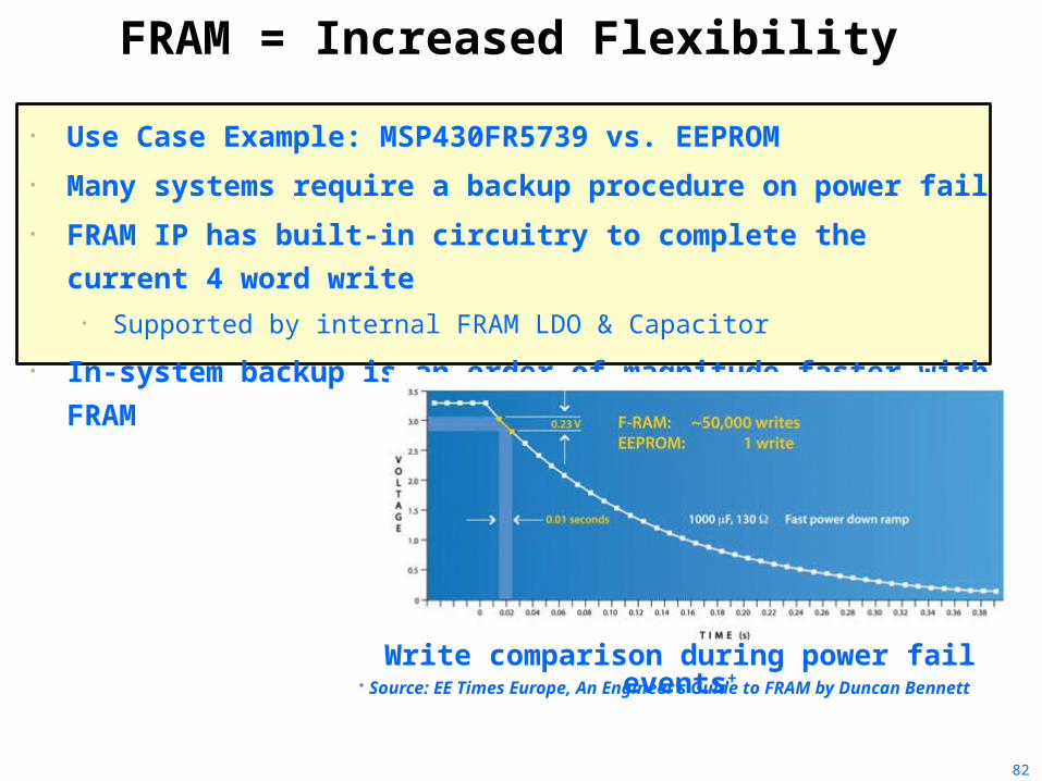
• Use Case Example: MSP430FR5739 vs. EEPROM• Many systems require a backup procedure on power fail• FRAM IP has built-in circuitry to complete the current 4 word write
• Supported by internal FRAM LDO & Capacitor
• In-system backup is an order of magnitude faster with FRAM
+ Source: EE Times Europe, An Engineer’s Guide to FRAM by Duncan BennettWrite comparison during power fail events+
FRAM = Increased Flexibility
82
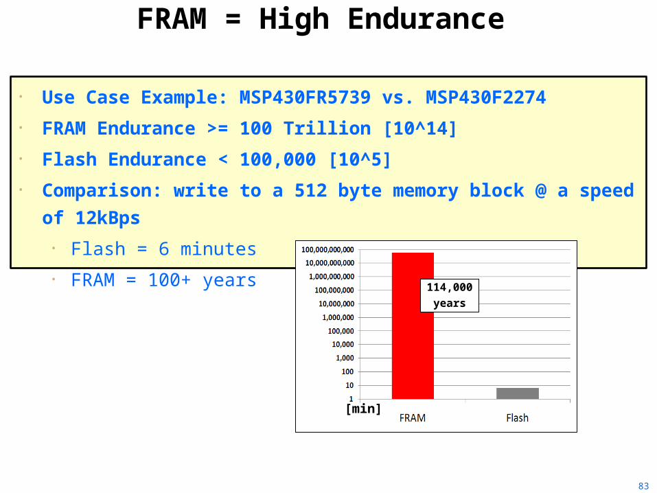
• Use Case Example: MSP430FR5739 vs. MSP430F2274• FRAM Endurance >= 100 Trillion [10^14]• Flash Endurance < 100,000 [10^5]• Comparison: write to a 512 byte memory block @ a speed of 12kBps
• Flash = 6 minutes• FRAM = 100+ years
FRAM = High Endurance
114,000years
[min]
83
What about Reflow? TI factory programming is not available for the MSP430FR57xx devices
Customer and CMs should program after reflow or other soldering
activity
TI will provide reference documentation that should be followed during
reflow soldering activity
Hand soldering is not recommended. However it can be achieved by
following the guidelines
Be mindful of temperature: FRAM can be effected above 260 deg
C for long periods of time
Using a socket to connect to evaluation board during prototyping
is also a best practice
84
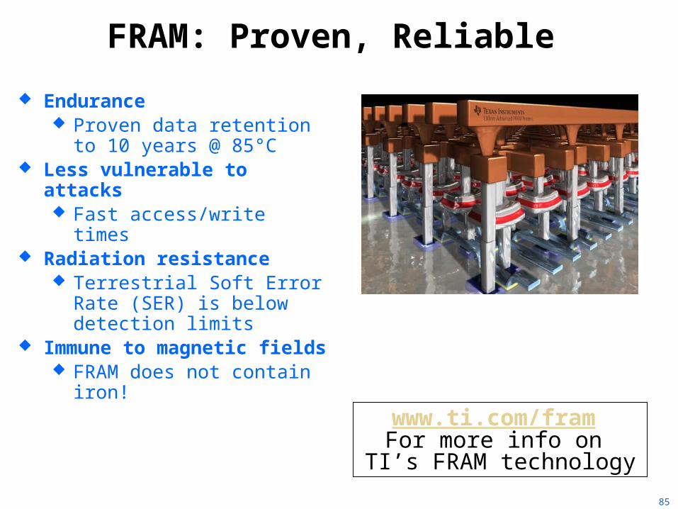
FRAM: Proven, Reliable Endurance
Proven data retention to 10 years @ 85°C
Less vulnerable to attacks Fast access/write times
Radiation resistance Terrestrial Soft Error Rate
(SER) is below detection limits Immune to magnetic fields
FRAM does not contain iron!
www.ti.com/fram For more info on
TI’s FRAM technology
85

Agenda
What is Capacitive Touch?
Introduction to Value LineCode Composer StudioInitialization and GPIO
Analog-to-Digital ConverterInterrupts and the TimerLow-Power OptimizationSerial Communications
GraceFRAM
Optional: Capacitive Touch
86

What is Capacitive Touch?
text
C1 C2
C3 C4
A change in Capacitance …
When a conductive element is present - Finger or stylus• Add C3 and C4, resulting in an increase in capacitance C1 + C2 + C3||C4• This becomes part of the free space coupling path to earth ground
When the dielectric (typically air) is displaced• Thick gloves or liquid results in air displacement and change in dielectric• Capacitance is directly proportional to dielectric, capacitance (C2) increases (air
~1, everything else > 1)
Options …87

MSP430 Capacitive Touch MethodsPin oscillator method (PinOsc with internal RO)No external components requiredTimer usedCurrently MSP430G2xx2 and MSP430G2xx3
1uA/Button
10uA/Button
< 3uA/Button
RO method Most robust against interferenceTimer used, comparator usedMSP430 devices with comparator
RC method Lowest power methodSupports up to 16 keysGPIO plus timer usedAny MSP430 device
Capacitive Measurement …88
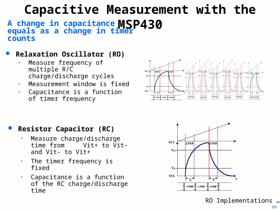
Capacitive Measurement with the MSP430
t
VIT-
VCC
VSSt+
TAR TAR
LPM0A
ctiv
e
Act
ive
LPM3 LPM0
Act
ive
Act
ive
VIT+
t-
Relaxation Oscillator (RO)• Measure frequency of multiple R/C
charge/discharge cycles • Measurement window is fixed• Capacitance is a function of timer
frequency t
VIT-
VCC
VSSt+
TAR TAR
LPM0
Active
Active
LPM3 LPM0
Active
Active
VIT+
t-t
VIT-
VCC
VSSt+
TAR TAR
LPM0
Act
ive
Act
ive
LPM3 LPM0
Act
ive
Act
ive
VIT+
t- t
VIT-
VCC
VSSt+
TAR TAR
LPM0
Ac
tiv
e
Ac
tiv
e
LPM3 LPM0
Activ
e
Ac
tiv
e
VIT+
t-t
VIT -
VCC
VSSt+
TAR TAR
LPM0
Ac
tive
Ac
tiv
e
LPM3 LPM0
Ac
tive
Ac
tiv
e
VIT+
t-t
VIT-
VCC
VSSt+
TAR TAR
LPM0
Active
Activ
e
LPM3 LPM0
Active
Active
VIT+
t- t
VIT-
VCC
VSSt+
TAR TAR
LPM0
Ac
tiv
e
Ac
tive
LPM3 LPM0
Ac
tive
Ac
tive
VIT+
t-t
VIT-
VCC
VSSt+
TAR TAR
LPM0
Active
Active
LPM3 LPM0
Active
Active
VIT+
t-
A change in capacitance equals as a change in timer counts
Resistor Capacitor (RC)• Measure charge/discharge time from
Vit+ to Vit- and Vit- to Vit+• The timer frequency is fixed• Capacitance is a function of the RC
charge/discharge time
RO Implementations …89
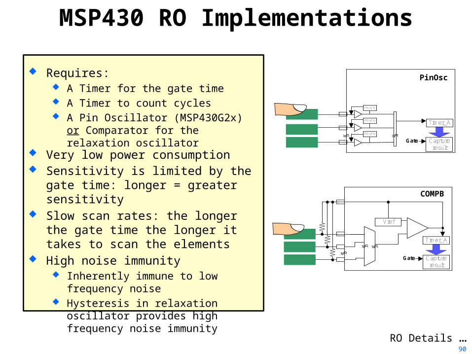
MSP430 RO Implementations
Captureresult
Timer_A
Gate
Vref
Requires: A Timer for the gate time A Timer to count cycles A Pin Oscillator (MSP430G2x) or
Comparator for the relaxation oscillator Very low power consumption Sensitivity is limited by the gate time:
longer = greater sensitivity Slow scan rates: the longer the gate
time the longer it takes to scan the elements
High noise immunity Inherently immune to low frequency
noise Hysteresis in relaxation oscillator
provides high frequency noise immunity
Captureresult
Timer_A
Gate
PRxEN
PRxEN
PRxEN
COMPB
PinOsc
RO Details …90
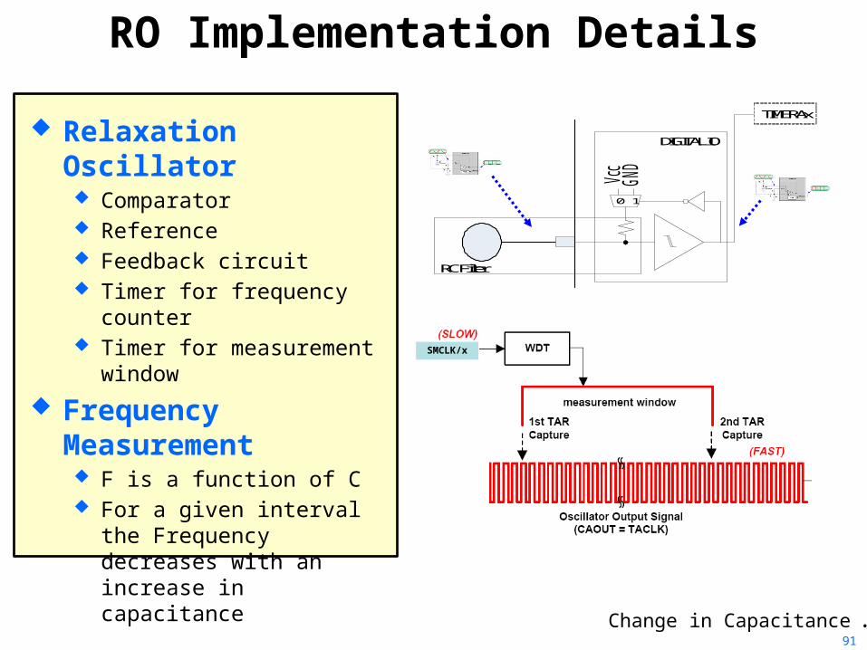
RO Implementation Details
Relaxation Oscillator Comparator Reference Feedback circuit Timer for frequency counter Timer for measurement
window Frequency
Measurement F is a function of C For a given interval the
Frequency decreases with an increase in capacitance
SMCLK/x
TIMERAx
RC Filter
Vcc
GN
D
DIGITAL IO
0 1
Change in Capacitance …91
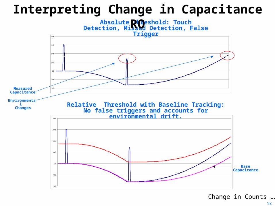
9.6
9.8
10
10.2
10.4
10.6
10.8
9.6
9.8
10
10.2
10.4
10.6
10.8
Measured Capacitance
Base Capacitance
Environmental Changes
Absolute Threshold: Touch Detection, Missed Detection, False Trigger
Relative Threshold with Baseline Tracking: No false triggers and accounts for environmental drift.
Interpreting Change in Capacitance RO
Change in Counts …92
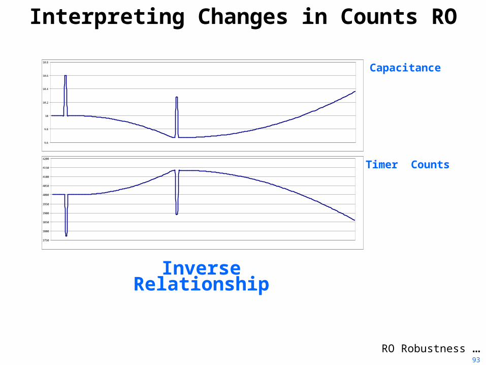
Interpreting Changes in Counts RO
9.6
9.8
10
10.2
10.4
10.6
10.8
Capacitance
3750
3800
3850
3900
3950
4000
4050
4100
4150
4200
Timer Counts
Inverse Relationship
RO Robustness …93
RO Robustness
SMCLK (Hz)
R (ohms)
Capacitance Change (11pF-11.22pF)
Gate Time (ms)
Change in Counts
Margin (threshold is 150)
1.00E6 35000 2% 8.192 301 50.2%
1.06E6 35000 2% 7.728 284 47.2%
0.94E6 35000 2% 8.7415 320 53.1%
1.06E6 50000 2% 7.728 199 24.6%
0.94E6 20000 2% 8.7415 560 73.2%
Limit the variables to capacitance– DCO calibrated constants +/-6% over Vcc and temperature– Integrated Resistance varies from 20Kohms to 50Kohms
RO Noise Immunity …94
RO Noise Immunity
Hysteresis Noise must occur at the relaxation oscillator frequency in order to
influence measurement Noise must be fairly large in magnitude to overcome hysteresis
(typically 1V) Natural Integration and Filtering
Gate window of milliseconds represents many charge/discharge cycles of the relaxation oscillator
Example: 2mS*1.8Mhz = 3600 cycles (samples) Baseline Tracking automatically calibrates system
Slowly tracks changes, filtering noise
PinOsc CPU Overhead …95
RO CPU Overhead Using PinOsc
99% of the measurement time is performed in a low power mode with no CPU interaction
RO integration performed 100% in hardware Calculation dependent on number of sensors, typically <<1% CPU available for other tasks
RC Implementation …96
MSP430 RC Implementation Timer and comparator or Schmidt trigger
GPIO Timer capture inputs Comparator Inputs
Simple interface Two sensor scan share a single resistor
Very, very low power consumption Sensitivity is limited to clock speed
2xx family 16Mhz 5xx 25MHz Timer D 256Mhz
Thick laminates require faster clock or other additional processing
Fast scan rates Poor noise immunity and not
recommended for applications that are connected to mains
Delta TAR
Timer_ADCO
Changes in Counts …97
Interpreting Changes in Counts: RC
9.6
9.8
10
10.2
10.4
10.6
10.8
Capacitance
3800
3850
3900
3950
4000
4050
4100
4150
4200
4250
4300
Timer Counts
Direct Relationship
Duty Cycle vs. Current …98
Importance of Duty Cycle vs. Current
Sleep Time (LPM3)Gate Time
Processing Time(Active)
1/Scan Rate
Cur
rent
PinOsc RO Current Gate
PinOsc 70uA 4ms
Sleep(LPM3) 0.7uA 96ms
1 Sensor @ 2Hz IntervalSensor = 70uA*0.008 ~ 0.60uASleep = 0.7uA*0.992 ~ 0.70uAAverage = ~ 1.30uA
Processing insignificant
Library Overview …99
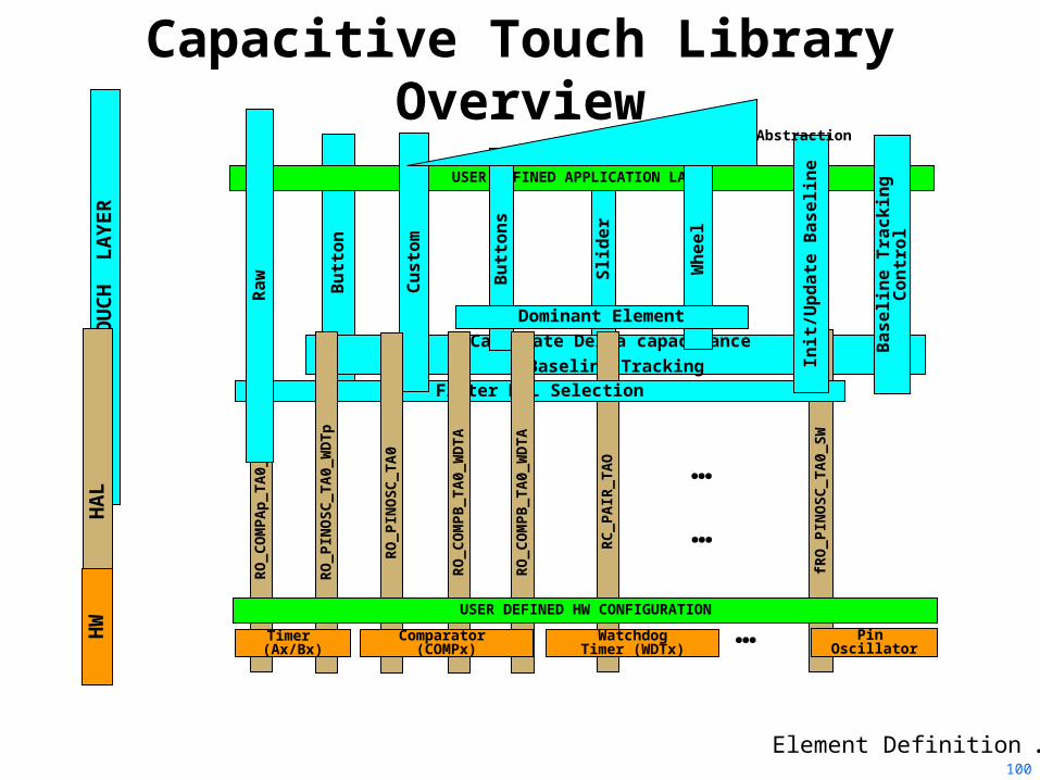
Capacitive Touch Library Overview
But
ton
Slid
er
USER DEFINED APPLICATION LAYER
Calculate Delta capacitance Baseline Tracking
RC
_PA
IR_T
AO
RO
_CO
MPA
p_TA
0_W
DTp
fRO
_PIN
OSC
_TA
0_SW
Whe
el
CA
P TO
UC
H L
AYER
HA
L
Filter HAL Selection
But
tons
Dominant Element
Cus
tom
Raw
RO
_PIN
OSC
_TA
0_W
DTp
RO
_CO
MPB
_TA
0_W
DTA
RO
_PIN
OSC
_TA
0
Init/
Upd
ate
Bas
elin
e
Bas
elin
e Tr
acki
ng C
ontr
ol
RO
_CO
MPB
_TA
0_W
DTA
USER DEFINED HW CONFIGURATION
Abstraction
Timer (Ax/Bx)
Comparator (COMPx)
WatchdogTimer (WDTx)
Pin Oscillator
…
…
HW …
Element Definition …100
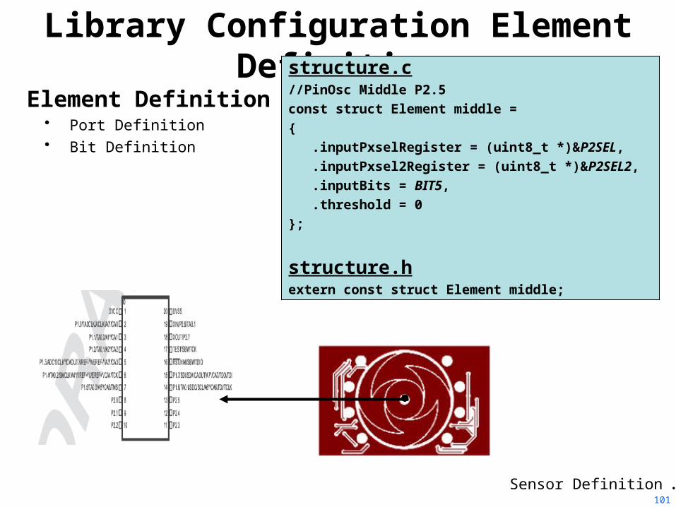
Library Configuration Element Definition
Element Definition• Port Definition• Bit Definition
structure.c//PinOsc Middle P2.5const struct Element middle = { .inputPxselRegister = (uint8_t *)&P2SEL, .inputPxsel2Register = (uint8_t *)&P2SEL2, .inputBits = BIT5, .threshold = 0 };
structure.hextern const struct Element middle;
Sensor Definition …101
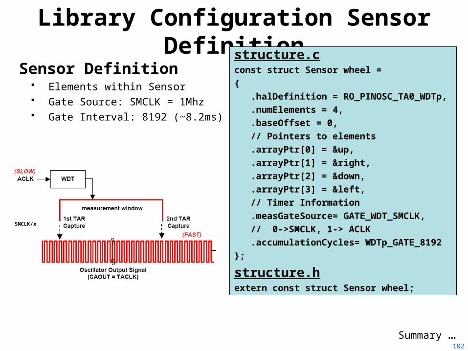
Library Configuration Sensor Definition
Sensor Definition• Elements within Sensor • Gate Source: SMCLK = 1Mhz• Gate Interval: 8192 (~8.2ms)
structure.cconst struct Sensor wheel ={ .halDefinition = RO_PINOSC_TA0_WDTp, .numElements = 4, .baseOffset = 0, // Pointers to elements .arrayPtr[0] = &up, .arrayPtr[1] = &right, .arrayPtr[2] = &down, .arrayPtr[3] = &left, // Timer Information .measGateSource= GATE_WDT_SMCLK, // 0->SMCLK, 1-> ACLK .accumulationCycles= WDTp_GATE_8192 };
structure.hextern const struct Sensor wheel;
SMCLK/x
Summary …102
Summary Capacitive Touch solutions can be implemented in a number of
ways on the MSP430 Tradeoff between available peripherals, IO requirements, sensitivity, and
power consumption Capacitive Touch IO (PinOsc function of the digital IO peripheral) in the Value
Line family is the most recent peripheral addition. No external components or connections Low power implementation of the relaxation oscillator
The Capacitive Touch library offers several levels of abstraction for different capacitance measurement applications Raw capacitance measurements Measurements with integrated baseline tracking Button, wheel, and slider abstractions
Download library and examples from www.ti.com/captouch
Layout…103
P2.0 (proximity)
P2.5(middle)Wheel
P2.4 (up)P2.1 (left)
P2.3 (right)P2.2 (down)
Capacitive Touch BoosterPack Layout
6 touch sensors Cap touch IOs create RO (PinOsc) 9 LEDs
Lab 10 …104
Lab10: Capacitive Touch
Lab10a: Observe element responseLab10b: Characterize the elementsLab10c: Implement a simple touch key application
105

106