George Heron, N2APB - Midnight Design...
18
DDS-60 Assembly & User Manual DDS-60 Assembly & User Manual, v1.3 1 Copyright 2005, AmQRP, All rights reserved ... a modular way to add stable DDS-based signal generation to your next transceiver or VFO project How many ways can you use a self-contained, high-precision dc-60 MHz signal source contained on a 1” x 2” plug-in circuit board? How about as a stand-alone VFO, a signal generator for your bench, a replacement LO for your Sierra or NC40 transceiver, or perhaps as the heart of an antenna analyzer! Control it with your favorite microcontroller, or even hang it off the parallel port of your PC. Any way you do it, you’ll be generating quality signals for less than $30. DDS-60 Front Side (NOTES: R19 and C5 happen to be installed in reversed positions on the board in this photo. The circuit is electrically equivalent. R16 and the IC shown on the right are no longer provided in the kit.) DDS-60 Bottom Side (NOTES: R7 and C4 positions are empty. These components are unused and are not provided in the kit.). Direct Digital Synthesis (DDS) captures the experimenter’s imagination and excites like no other technology these days. Exceptional signal precision, accuracy, stability, programmability and signal quality are all easily and inexpensively achieved. But two quite formidable problems still remain. The first problem is that these surface mount DDS chips are so tiny, with lead pitches as fine as 0.65 mm, that it is nearly impossible to homebrew with them using conventional techniques. It is quite difficult to tack- solder a fine wire onto one of these small SOIC package leads, let alone putting 16 wires to the chip! The second problem is that these DDS chips must be interfaced to a microcontroller that provides that frequency programmability. A 40-bit control word must be loaded into the DDS chip to command it to generate a specific frequency. There are many projects around that control a DDS chip with a PIC, an Atmel controller, a BASIC Stamp, an SX chip, and so on. I don’t know about you, but the VFO I will ultimately need is likely to use some controller that I don’t technically “know” and cannot program. This makes it tough to use that controller for anything but commanding the DDS, thus raising the cost of the entire project, increasing the amount of board real estate needed, and raising the power needs for the entire project. The Solution To get past these two problems, we designed the “DDS-60” – a self-contained functional module that generates a top-notch RF signal by using a small pc board to contain just the bare DDS essentials: an Analog Devices AD9851 DDS chip, a clock oscillator, a 5 th -order elliptic filter and an adjustable-level RF amplifier. Additionally, an onboard 5V regulator is provided so you only need provide a single 12V battery or power supply ranging anywhere from 8-16V DC. The three digital control lines, the power supply, and the output signal are all available on a pin header at the board edge. This 8-position pin header serves to allow the DDS-60 to be plugged into and used in many projects on your bench, regardless of which microcontroller is employed. Just provide a single strip socket (e.g., a 16-pin IC socket split lengthwise) on the project board and plug in the DDS- 60. A cable connected to the parallel printer port of your PC can even be used in conjunction with public domain
-
Upload
vuongduong -
Category
Documents
-
view
220 -
download
4
Transcript of George Heron, N2APB - Midnight Design...

DDS-60 Assembly & User Manual
DDS-60 Assembly & User Manual, v1.3 1 Copyright 2005, AmQRP, All rights reserved
... a modular way to add stable DDS-based signal generation to your next transceiver or VFO project
How many ways can you use a self-contained, high-precision dc-60 MHz signal source contained on a 1” x 2” plug-in circuit board? How about as a stand-alone VFO, a signal generator for your bench, a replacement LO for your Sierra or NC40 transceiver, or perhaps as the heart of an antenna analyzer! Control it with your favorite microcontroller, or even hang it off the parallel port of your PC. Any way you do it, you’ll be generating quality signals for less than $30.
DDS-60 Front Side (NOTES: R19 and C5 happen to be installed in reversed positions on the board in this photo. The circuit is electrically equivalent. R16 and the IC shown on the right are no longer provided in the kit.)
DDS-60 Bottom Side (NOTES: R7 and C4 positions are empty. These components are
unused and are not provided in the kit.).
Direct Digital Synthesis (DDS) captures the experimenter’s imagination and excites like no other technology these days. Exceptional signal precision, accuracy, stability, programmability and signal quality are all easily and inexpensively achieved. But two quite formidable problems still remain. The first problem is that these surface mount DDS chips are so tiny, with lead pitches as fine as 0.65 mm, that it is nearly impossible to homebrew with them using conventional techniques. It is quite difficult to tack-solder a fine wire onto one of these small SOIC package leads, let alone putting 16 wires to the chip! The second problem is that these DDS chips must be interfaced to a microcontroller that provides that frequency programmability. A 40-bit control word must be loaded into the DDS chip to command it to generate a specific frequency. There are many projects around that control a DDS chip with a PIC, an Atmel controller, a BASIC Stamp, an SX chip, and so on. I don’t know about you, but the VFO I will ultimately need is likely to use some controller that I don’t technically “know” and cannot program. This makes it tough to use that controller for anything but commanding the DDS, thus raising the cost of the entire project, increasing the amount of board real estate needed, and raising the power needs for the entire project. The Solution To get past these two problems, we designed the “DDS-60” – a self-contained functional module that generates a top-notch RF signal by using a small pc board to contain just the bare DDS essentials: an Analog Devices AD9851 DDS chip, a clock oscillator, a 5th-order elliptic filter and an adjustable-level RF amplifier. Additionally, an onboard 5V regulator is provided so you only need provide a single 12V battery or power supply ranging anywhere from 8-16V DC. The three digital control lines, the power supply, and the output signal are all available on a pin header at the board edge. This 8-position pin header serves to allow the DDS-60 to be plugged into and used in many projects on your bench, regardless of which microcontroller is employed. Just provide a single strip socket (e.g., a 16-pin IC socket split lengthwise) on the project board and plug in the DDS-60. A cable connected to the parallel printer port of your PC can even be used in conjunction with public domain

PC software to control the DDS-60. See the Controller section in the full manual for a number of custom solutions illustrating easy control of the DDS-60.
Once your controller-of-choice serially loads the control word into the DDS, the raw waveform is generated and presented to an elliptic filter that removes unwanted high-end frequency components, resulting in a signal of sufficient quality to serve as a local oscillator for a transceiver. We regularly see great signal quality, with harmonic content typically more than 40 dB below the fundamental. The signal generated by the DDS is quite small so we use an AD8008 low power amplifier to provide about 18 dB of gain to boost the signal to about 2V-to-3V p-p, which is quite usable in a variety of applications. This amplifier chip offers unconditional stability (k>1) and yields spectrally-clean signals. It is an ideal signal source for making impedance measurements in the Micro908 Antenna Analyst and other demanding applications. A trimpot allows precise manual control of the desired output level. The design provides a good signal using supply voltages from 16V all the way down to 8V, thus conveniently allowing for battery operation. The amplified signal is then available for use as a 50-ohm source input signal. If not used as an input to any other component or module, the output should be terminated with a 50-ohm load for the stated specifications to be realized.
Specifications
Power requirements: 8-16V DC at 120 ma (typ). RF Output – fully adjustable, up to +15 dBm (about 3V pp) Output signal unaffected by varying +V supply voltage – great for battery operation. Near-constant output level from 1-60 MHz Good signal purity – harmonics down approximately 40 dB from the fundamental.
DDS-60 Assembly and User Manual v1.3 2 Copyright 2005, AmQRP, All rights reserved

DDS-60 Assembly and User Manual v1.3 3 Copyright 2005, AmQRP, All rights reserved

DDS-60 Daughtercard Parts List:
QTY Designator Description3 R1, R5, R12 Resistor, 51 ohms, 1/4 W, 5%, SMD 12061 R2 Resistor, 470 ohms, 1/4 W, 5%, SMD 12061 R3 Resistor, 620 ohms, 1/4 W, 5%, SMD 12063 R4, R17, R18 Resistor, 200 ohms, 1/4 W, 5%, SMD 12062 R6, R9 Resistor, 1 K ohms, 1/4 W, 5%, SMD 12061 R19 Resistor, 100 ohms, 1/4 W, 5%, SMD 12061 R8 Trimpot, 500 ohms, SMD1 R10 Resistor, 5.6 K ohms, 1/4 W, 5%, SMD 12061 R11 Resistor, 24 ohms, 1/4 W, 5%, SMD 12063 R13, R14, R15 Resistor, 10 K ohms, 1/4 W, 5%, SMD 1206
12 C1, C2, C3, C5, C7, C9, C10, C17, C18, C19, C20, C21 Capacitor, 0.1 uF, 25 V, ceramic, X7R, 1206
1 C6 Capacitor, 0.22 uF, 50 V, ceramic, X7R, SMD 12061 C8 Capacitor, electrolytic, SMD, 1.0 uF, 50V1 C12 Capacitor, 47 pF, 50 V, ceramic, NPO, SMD 12062 C13, C15 Capacitor, 15 pF, 50 V, ceramic, NPO, SMD 12061 C14 Capacitor, 100 pF, 50 V, ceramic, NPO, SMD 12061 C16 Capacitor, 82 pF, 50 V, ceramic, NPO, SMD 12062 L1, L2 Inductor, 0.10 uH, iron, SMD 12061 U1 AD8008, IC curr-fdbk amp dual 8-SOIC1 U2 AD98511 U3 UA78MO5 IC voltage regulator, f ixed pos SOT-2231 U4 Reference Oscillator 30.000 MHz SMT1 P1 Pin Header, 0.1", 8 pin1 PCB PC Board
1.
2.
3.
4.
5.
6.
7.
Assembly Steps
Need help assembling all these small components? See the comments in the Notes section about Kit Builders.
Attach all SMT integrated circuits. For each IC location, tin pad 1, carefully position the IC observing orientation, and solder pin 1 in place. Solder the opposite-corner pin while ensuring that all pins are over the respective pads. Solder remaining pins to pads. If needed, remove excess solder with solder braid. (Solder the larger ground tab of U3 to the pad opposite the three smaller pins.)
Attach trimpot R8 by tinning one pad first, then carefully hold the trim pot in place with tweezers, and re-heat the pad. Solder the other two pads. Measure about 250 ohms from wiper pad to either end pad to ensure successful connection.
Attach all SMT resistors. Sequentially attach each value group to the board, according to the order arranged on the SMT Card. For each resistor location, tin one pad, hold resistor in place and reheat that pad to attach. Solder other end to pad.
Attach all SMT capacitors in the same manner as above.
Attach inductors L1 and L2 in the same manner as above.
Attach capacitor C8 (silver can) in same manner as above. Side without black mark goes to + pad.
8.
9.
Attach oscillator U4 with notched end “up”. See photo.
DDS-60 Assembly and User Manual v1.3 4 Copyright 2005, AmQRP, All rights reserved
Attach pinheader P1 to the top of board – see photo.

10. Install jumpers at the ‘a’ set of pads. (The ‘b’ set of pads are for an option that is no longer offered.)
Initial Test & Adjustment
1.
2.
3.
4.
1.
2.
Observe P1 connections and apply 8-16V dc power.
Observe approx 5V p-p clock waveform at U4 output.
While driving DDS-60 card with appropriate controller generating 10 MHz waveform, observe ~200mV p-p at DDS output and at R1/C1 input to RF amp.
Adjust R8 to obtain approx 2V-to-3V p-p at RF Out.
Troubleshooting Here are some checks you might try if you think your DDS-60 card is not functioning.
You should ideally have a 2V p-p RF signal at the output of the board when driving a 50-ohm load. The signal can be adjust from near-zero all the way up to over 3V p-p … the default/initial mid-position trimpot setting will yield about 2V p-p, as seen on an oscilloscope; or using an RF probe on your DVM, this will be somewhere between 0.7 Vdc and 0.4 Vdc RMS, depending on the frequency of the sine wave, the type of RF probe you have and the input impedance of your DVM to which the RF probe is attached.
DDS-60 Assembly and User Manual v1.3 5 Copyright 2005, AmQRP, All rights reserved
Carefully turn the trimpot throughout its range while looking for the signal. If you do not see a signal there on P1p6, then your DDS-60 card is not generating a signal.

3. Probe "backwards" through the circuit to see where you do see the signal. You should have that same signal level (0.4 to 0.7 RMS) at the output of U1b pin 7. If you do, the problem is between there and the board output.
4.
5.
If you do not, check the next amp output back in the chain: U1a pin 1. You should expect to see about half of what the expected board output was: about 0.9V p-p, or 0.3V DC with your RF probe (again depending on the RF probe and DVM used). And again carefully turn the trimpot while looking for the voltage.
If you do not see a signal there on U1a pin 1, then the problem is farther back toward the DDS. But if you do see a signal, the problem is somewhere between the two amplifiers U1a and U1b. Carefully look for wrong components placed, improperly soldered components, and missing/broken components.
6.
7.
8.
Next, look for a 200 mV p-p signal (0.07 Vdc on your RF Probe + DVM) at the output of the Low Pass Filter. The output of the LPF is on the through-hole pad below the right end of C1. If you see the signal there, the problem is probably in the first amplifier stage (U1a). Again check components, etc., as previously instructed.
Next, look for the raw DDS output signal, also 200 mV p-p at the top of R12. If you do not see a signal there then the DDS is not DDS'ing.
Next, check to see that your reference clock is producing the required 30 MHz signal to the DDS chip. Probe the larger through-hole pad to the left of C19 and expect to see a whopping signal of about 4 Vp-p, or 1.4 Vdc with your RF probe and DVM. If not seen, your reference clock isn't attached properly or it is defective - either of which would inhibit your DDS card from working.
Temperature Analysis
Some builders of the DDS-60 card are surprised at how hot the components operate, particularly the DDS chip (U2) and the 5V voltage regulator device (U3). In quick summary, these components will indeed get pretty warm – in fact too warm to hold your finger on it for more than 5-10 seconds – but this is quite normal and here is how we determine that:
DDS-60 Assembly and User Manual v1.3 6 Copyright 2005, AmQRP, All rights reserved
DDS-60 card: Input: 13.4 volts, 128 ma - Don't forget there's a diode between the power connector & card, amounting to a 0.2 volt drop. - This current is for fully operating DDS chip, with PLL turned on effectively creating a 180 MHz ref clock Regulator: Input: 13.4 volts Output: 5 volts, 97 ma Tj(max) = 150-degC Theta-JA = 53-degC AD9851: Power: 650 mW (worst case from spec sheet, 180 MHz @ 5V) Tj (max) = 150-degC Theta-JA = 82-degC Ambient Temp = 21.1-degC - - - - - - - - - - - Theta-JA = Thermal resistance from junction-to-ambient The all-important equation for Tj (temp of internal semiconductor junction): Tj = Tambient + (PWR x Theta-JA) - - - - - - - - - - - So for the REGULATOR ... Tj = 21.1 + (((13.4 - 5) x .097) x 53) = 64.3-degC

... therefore, compared to Tj(max) of 150, we are well within spec. And for the AD9851 ... Tj = 21.1 + (.650 x 82) = 74.4-degC ... therefore again, compared to Tj(max) of 150, we are well within spec. - - - - - - - - - - - Temperature Measurements .... Tambient = 21.1-degC (70-degF) Regulator case = 71.1-degC (160-degF) (Regulator heatsink tab) = 76.6-degC (170-degF) AD9851 case = 63.9-degC (147-degF) - - - - - - - - - - - Conclusions ...
1) The DDS-60 is operating within component thermal and power specifications.
2) The "too hot to touch" observation that some have made is probably correct. Even my guitar-calloused fingers cannot be pressed on either of these chips for longer than 10 seconds without a severe "Ouch!". But this is normal and okay, as long as the ambient temperature stays below 195-degF (yes, an almost-boiling room temperature will exceed the max Tj of these components!) The packages are made for this ... our fingers are not.
3) If you want to reduce the operating temperature of the voltage regulator (U3), try supplying the DDS card with a lower voltage. The card is designed to operate with a voltage source as low as 8V. Using this level of power supply will significantly lower the operating temperature of the regulator.
PS: Voltage, current and temperature measurements were made with a Metex ME-11 DVM with a Fluke 80T-150U temperature probe.
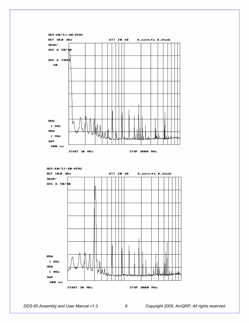
DDS Signal Quality
Jim Kortge, K8IQY performed some signal quality measurements using his lab-quality spectrum analyzer and he captured the screen views for us. Jim writes …
DDS-60 Assembly and User Manual v1.3 7 Copyright 2005, AmQRP, All rights reserved
“Guys, I thought you might like to have the latest plots at 10, 30, and 60 MHz using the latest PIC-EL 5.1 code and my DDS-60. I also just ran a test to make sure that the manual gain pot could be used to adjust the 60 MHz amplitude to that of the 10 MHz signal. Works like a dream! I think this DDS-60 board is a true winner and works very well.”
DDS-60 Assembly and User Manual v1.3 8 Copyright 2005, AmQRP, All rights reserved

Controlling the DDS It won’t be too long before you consider ways to use the DDS-60. Well, you are in for a real treat as there are a whole bunch of convenient and powerful techniques already developed that can be employed to provide a user interface and controller for this RF signal generator module. In general, the AD9851 DDS chip needs to be sent a control word by an external controller before the DDS-60 is capable of generating a signal. No matter what controller you use, it must serially send a 40-bit control word to the DDS-60 on the DATA line (P1 pin 3). The controller clocks each bit into the DDS chip by the toggling the CLK control line (P1 pin 2). To complete the sequence, the accumulated control word is loaded into another internal DDS register by a toggling of the LOAD line (P1 pin 1), thus instructing the DDS chip to generate the frequency just loaded. Then bingo, the new frequency appears at the RF Output of the DDS-60 card (P1 pin 6). The AD9851 data sheet, and an Interactive Design Tool applet on the Analog Devices website:
http://www.analog.com/Analog_Root/static/techSupport/designTools/interactiveTools/dds/ad9851.html provide all the details on how to construct the five byte, 40-bit control word with your microcontroller-of-choice. Just select 5V operation, enter 30 MHz in the reference clock field, select the 6x multiplier, and the desired operating frequency. The applet will display the five control bytes that you need to send serially to the DDS-60 in order for it to generate that frequency. There are many software programs available that already accomplish sending the control words to the DDS card, thus enabling it to serve as a general purpose VFO. Any of the techniques outlined in the next section may be adopted if you plan on using the specific processors in your project. They are also great examples on which you can model a software program using a different microcontroller.
Here are some great ways for you to build up a project using the DDS-60 card to generate AF and RF signals.
DDS-60 Assembly and User Manual v1.3 9 Copyright 2005, AmQRP, All rights reserved

PIC-EL
The PIC-EL is a multi-function PIC16F84A-based project board that serves as the basis for the instruction and experiments being conducted in the online PIC Elmer 160 course. The course material is geared around use of common I/O components -- pushbuttons, LEDs, LCD display, rotary encoder and speaker. It has a built-in serial programmer that allows the user to download new programs directly from the PC and "burn" them into the PIC microcontroller, and we provide an ability for the user to plug in the inexpensive and ubiquitous DDS-60 card that produces signals up to 60 MHz. A rotary encoder "dial" allows one to use the PIC-EL as a stable signal general, a super precise VFO or perhaps even as a signal source for receiver calibration. A BNC connector is also provided in the kit to help enable these common uses. The PIC-EL can measure the frequency of an input signal presented on the BNC connector. Stereo 1/8” jacks allow you to plug in your iambic paddles and have the project board serve as a keyer with adjustable speed, weighting and multiple memory buffers. The onboard speaker serves as a side tone and you can connect the "keyline" output signal to your rig by cabling from the other 1/8" jack and you'll be able to key your rig with the PIC-EL project board.
DDS card plugged into the PIC-EL project board. (The DDS card shown here is the original “DDS-30” Daughtercard … the new DDS-60 card is plug-compatible on the PIC-EL hardware.
DDS-60 Assembly and User Manual v1.3 10 Copyright 2005, AmQRP, All rights reserved

QuickieLab The DDS-60 is ready-made for plugging into the NJQRP “QuickieLab”, which is an experimenter’s platform provided several years ago in kit for hobbyists to easily build up circuits on a plugboard and connect them into various standard circuits provided on the board for audio amplification, A/D conversion and LCD display. So all you need to do is plug the DDS-60 into the appropriate socket on the QuickieLab and use some of the canned software that’s provided to have the hardware serve as a basic VFO. The programming sequence is easily accomplished. In one of his renowned “Joe’s Quickies” columns in QRP Quarterly magazine, N2CX uses the following three lines to instruct the BASIC Stamp controller to produce a 7.040 MHz signal with the DDS-60 plugged into the QuickieLab:
shiftout 7,8,0,[$8F,$2F,$03,$0A,$01] out9 = 1 out9 = 0
The first instruction line shifts out the 40-bit (5-byte) value on port P7 using P8 as the clock. The Mode we use for the shiftout command is ‘0’, meaning that the LSB gets shifted out first for each data byte listed in parentheses, starting with the first byte listed (8F) and ending with the last byte (01). This is the bit programming order specified for the AD9850 and AD9851 in serial mode. The second and third instruction lines toggle the LOAD pin going to the DDS, at which point the RF signal is generated at the output of the DDS-60. (If you do use the DDS Daughtercard with the NJQRP QuickieLab, remember to cut the +5V trace on the bottom of the QuickieLab pc board that leads to P1 pin 4 on the DDS-60 socket. This is because the DDS-60 produces its own internal 5V supply and doesn’t require the QuickieLab to supply it.)
Here’s the QuickieLab set up with the DDS Daughtercard (the previous version “DDS-30” card is shown) in the socket located just above the white plugboard. The BASIC Stamp processor, located on the main board beneath the LCD, commands the DDS chip on the daughtercard in order to generate RF signals that are pumped out the BNC connector on the right side of the board.
DDS-60 Assembly and User Manual v1.3 11 Copyright 2005, AmQRP, All rights reserved

Closeup of the DDS Daughtercard plugged into the QuickieLab.
Note that DDS card used here is one of the original ones that used the MMIC amplifier on the right side of the card. (The MMIC amplifier
DDS-60 Assembly and User Manual v1.3 12 Copyright 2005, AmQRP, All rights reserved
has been replaced by the addition of the AD8008 in the current DDS-60 design.)

Butterfly Controller Board Software currently exists for the AVR Butterfly card to present a simple user interface for frequency entry and display and to command the DDS Daughtercard to generate those frequencies. See http://www.atmel.com/dyn/products/tools_card.asp?tool_id=3146) for more information on the Butterfly controller card. Steve Weber, KD1JV developed the DDS card driver software and has it on his website, located at http://www.qsl.net/kd1jv/bfydds.HTM.
The “Butterfly” controller card from Atmel is a convenient and inexpensive
way to get a fairly powerful processor on a card with some universal I/O of an LCD and “joystick/pushbutton” being used to navigate.
Here is pictured the DDS Daughtercard plugged into an ERCOS
Butterfly Carrier board, which allows the Atmel processor to control circuits interfaced to the Butterfly board. The additional circuit card
on the right is an earlier version of the SoftRock40 SDR receiver project described elsewhere in this issue of Homebrewer. In this
application, the Butterfly controller board controls the DDS Daughtercard to generate RF being used as the local oscillator
for the little receiver card. (The ERCOS Carrier Kit can be found at http://www.ecrostech.com/Products/Butterfly/Intro.htm)
DDS-60 Assembly and User Manual v1.3 13 Copyright 2005, AmQRP, All rights reserved

Micro908 The DDS Daughtercard is already incorporated into the Micro908 kit from the AmQRP Club and is integrally used to make the instrument function as an antenna analyzer. So if you are able to write a specific VFO program for the Micro908, or perhaps just use the VFO function provided with the AA-908 software load on the Micro908, you can use the instrument to generate signals “right out of the box”.
The DDS Daughtercard (identified by the white circle in the photo above) Is controlled by the HC908 Daughtercard on the Micro908 motherboard. It plugs into an 8-pin right-angle connector that holds the DDS card up off the motherboard, above the reflectometer circuits of the Micro908.
DDS-60 Assembly and User Manual v1.3 14 Copyright 2005, AmQRP, All rights reserved

HC908 Daughtercard You may also plug the daughtercard into the HC908 Excerciser board described in the Digital QRP Breadboard project and use the software provided with that project to have it serve as a programmable VFO.
The HC908 Daughtercard controller is a popular and recurring component with the DDS Daughtercard. Together they make a flexible combination of modules that can be used in many different applications, using a common set of software libraries (subroutines). The configuration of the two modules shown in the right photo is the minimal hardware arrangement needed for a “dumb terminal” (like HyperTerm on a Windows PC or ProComm on a handheld computer) to command the HC908 to generate frequencies … in effect, the HC908 and DDS daughtercards become a remotely-controlled signal generator!
DDS-60 Assembly and User Manual v1.3 15 Copyright 2005, AmQRP, All rights reserved

Parallel port control from your PC You can even control the DDS Daughtercard directly from your PC. All that’s needed is to wire the daughtercard to the printer port cable and run one of several public domain custom software programs to have the PC serve as VFO controller. The programs from KA2UPW, or WA6UFW and WA6FXT (located on the project website) each have an attractive display screen that offers specific frequency entry, phase settings, and even scanning controls!
If you wire the DDS Daughtercard to the PC’s parallel port connector and a power supply, as shown in this diagram, any signal from 0.1 Hz to 30 MHz may be generated by the software application running on the PC.
Here is shown the “PC VFO” assembly being controlled by a PC over its parallel printer port. The DDS Daughtercard is housed in a rugged die-cast aluminum enclosure with connectors for the parallel port control lines, RF output on a BNC, and power input on a coaxial power connector. Switches provide power control and the ability to switch a 50-ohm load resistor in/out of the circuit. The oscilloscope display in the background shows the nice and clean 10 MHz signal currently being generated by the DDS card, as commanded from the PC screen.
DDS-60 Assembly and User Manual v1.3 16 Copyright 2005, AmQRP, All rights reserved

Custom Controller Of course you can also design the DDS Daughtercard into your own custom project, using your favorite microcontroller chip as the “brains”, be it a PIC, Atmel, Ubicom, or 8051-derivative processor. The possibilities are limitless!
DDS-60 Assembly and User Manual v1.3 17 Copyright 2005, AmQRP, All rights reserved
This photo shows the DDS Daughtercard included in a circuit I call the Exerciser. It is a test fixture that all HC908 Daughtercards get plugged into for test and programming with the appropriate software before shipping. (The Exerciser schematic and software program are located in the HC908 Daughtercard manual.)

DDS-60 Assembly and User Manual v1.3 18 Copyright 2005, AmQRP, All rights reserved
Conclusion This simple DDS Daughtercard solves both of the problems described at the beginning of this article. It enables the homebrewer to easily take advantage of the positive attributes of the DDS chip to produce a high quality homebrew variable-frequency signal source. Let us know how you end up using your DDS ‘card!
NOTES 1. Getting a Free Sample of the AD9851 DDS Chip
The DDS chip is not provided in the kit – homebrewers can obtain a free sample from the Analog Devices website at: http://www.analog.com/en/prod/0%2C2877%2CAD9851%2C00.html#price (If AD changes the link around again on us, you can Google-search on “AD9851” and take the first link presented.) Just go to the “Price, Package, Availability” link, add the AD9851BRSZ or AD9851BRSZRL to your shopping cart, and follow directions for checking out. Within a week you will receive a free sample of the DDS chip by mail.
2. Need Help Attaching the Surface Mount Chips?
We’ve lined up a great resource to assist by soldering the SMT components onto the printed circuit board. Once you’ve acquired your free DDS chip from Analog Device, send the DDS chip and kit components to Mike WA6OUW, at “KitBuilders”. For a very reasonable price he will attach all components to the pc board and return it promptly by mail. Mike does excellent work at the assembly, while you finish off the project with test and installation. Contact “KitBuilders” at [email protected] for a quote and details, or by mail at KitBuilders, 6361 Berrybush Ct., Gilroy, CA 95020.
3. Technical Support
We maintain a Builders Notes page on the main DDS-60 web page http://www.amqrp.org/kits/dds60 that contains much useful kit information. If you still have questions or need technical assistance after consulting this online resource, contact: George Heron, N2APB ([email protected]), or Joe Everhart, N2CX ([email protected]).
4. The DDS-60 Kit may be purchased from the AmQRP Club. Refer to the DDS-60 project web page for all
current technical and ordering details: http://www.amqrp.org/kits/dds60/index.html.
5. The NJQRP has lined up a great resource to assist in soldering the DDS chip onto the printed circuit board. Once you’ve acquired your free AD9851BRS DDS chip from Analog Device, send the chip and your DDS Daughtercard circuit board, to Mike, WA6OUW, at “KitBuilders”. For $10 he will attach this surface mount chip to the pc board and return it promptly by mail. It’s not tested because at that point it’s only the DDS chip on a bare pc board, but Mike does excellent work. (The NJQRP uses KitBuilders for assembly of the HC908 Daughtercard product, so we know the quality is there!) Just place your DDS chip, pc boards and a $10 check or M.O. payable to “KitBuilders” into a padded envelope and send to: KitBuilders, 6361 Berrybush Ct, Gilroy, Ca. 95020. You can contact Mike by email at [email protected] if you have further questions.
6. Details of the NJQRP QuickieLab project can be found at www.njqrp.org/quickielab .
7. Details of the HC908 Daughtercard project can be found at www.njqrp.org/hc908 .