
Generation of High Intensity Positron Beam Using 20 MeV linac

CHAPTER 2
GENERATION AND APPLICATIONOF HIGH INTENSITY PULSEDELECTRIC FIELDSMarkus J. Loeffler
1. INTRODUCTION
The generation of pulsed electric fields at high-power levels is one of the tasks of pulsed powerengineers. In this chapter, we define pulsed power technologies to be those electrical devices that areused to treat organic and inorganic materials with electric fields> 10 kV/cm and/or magnetic fields> 10 T. As a rule, they work at power levels >0.1 GW, which are power levels that are not availablefrom small- or medium-sized conventional energy sources (Bodecker, 1985). Typical durations ofsingle or repetitive power pulses are in the range between nanoseconds and milliseconds. Most pulsedpower devices use capacitors to store electrical energy that is delivered to their respective electricloads via a high-power switch.
The energy stored in capacitors is used to generate electric or magnetic fields. Electric fieldsare used to accelerate charged particles, leading to thermal, chemical, mechanical, electromagneticwave, or breakdown effects. Electromagnetic fields transfer energy as electromagnetic waves. xray, microwaves, and laser beam generation are typical examples. Magnetic fields facilitate thegeneration of extremely high pressures ranging from 0.1 GPa to many GPa. These effects areapplied to modify molecules to remodell, compress, weld, segment, fragment, or destroy materials; and to modify the surface of organic and inorganic parts and particles (Weise and Loeffler,2001).
In general, those devices that are used to electrically pulse treat liquid foods or other aqueoussubstances have an electrode gap filled with a more or less conductive liquid. From an electricalpoint of view, these devices can be compared to water resistors driven either in the "normal operationmode" (e.g., electroporation) or in the "failure mode" (e.g., shock wave treatment). In the first case, acurrent is driven across the entire cross-section of the liquid, whereas in the second case an electricalbreakdown occurs followed by high intensity current flowing through the small cross-section of anarc. The specific power requirements of such "resistors" together with information about the requiredmass flux and the dimensions of the treatment zone define the type and the specific parameters ofthe power supply.
Markus J. Loeffler > High Voltage and Pulsed Power Technology, Energy Institute, University of Applied Sciences, Neidenburger Strasse 10, D-45877 Gelsenkirchen, Germany.
27

28
The objectives of this chapter are to provide basic information
1. about the power and energy requirements of PEF systems2. about high-power sources3. about low-power sources.
2. ELECTRIC LOAD REQUIREMENTS
Markus J. Loeffler
From the point of view of an electrical engineer, organic material in water is a bad insulatorsurrounded by a highly permittive medium, i.e., water. The effect of stressing organic materialsunder water with an electric field is shown in Fig. 2.1 (Loeffler et al., 2001). The rubber membranewas positioned between two electrodes under water. A voltage was applied between the electrodes.Because of the high permittivity of the water, the electric field was concentrated in the rubbermembrane itself thus causing electrical breakdown at several locations on the foil. Increasing thefield and the treatment time, increased the number of holes in the foil.
The electrical specifications of devices used to inactivate microorganisms by perforating theircell membranes require some fundamental information about their electric load: strength of theelectrical field, specific power consumption, mass flow rates, average power consumption, voltagewaveforms, and treatment durations. Because of the different treatment profiles needed for differentapplications, a "characteristic application" with "characteristic values" shall be defined by averagingand evaluating values and information gained from a large number of experiments published in theopen literature.
2.1. Specific Power Consumption
The specific power consumption of liquids treated with electrical pulses is defined by
• their specific electrical conductivity and• the electric field strength required to kill the cells contained in the liquid.
Figure 2.1. Effect of pulsed electric fields on rubber membrane under water.
2 • Generation and Application 29
municipal
water
tomatojuice'
1.5
(1 [SImI2
milk
/ 1.5% fat
/ orange/ // jUiCe
/// / apple.r > ./"./" jUice
05 < >" ./" _beer. / ./" -~ ./" ~ - -~ -
20 40 60 80 100
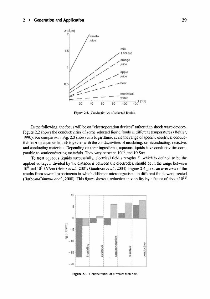
Figure 2.2. Conductivities of selected liquids.
In the following, the focus will be on "electroporation devices" rather than shock wave devices.Figure 2.2 shows the conductivities of some selected liquid foods at different temperatures (Reitler,1990). For comparison, Fig. 2.3 shows in a logarithmic scale the range of specific electrical conductivities a of aqueous liquids together with the conductivities of insulating, semiconducting, resistive,and conducting materials. Depending on their ingredients, aqueous liquids have conductivities comparable to semiconducting materials. They vary between 10-2 and 10 S/m.
To treat aqueous liquids successfully, electrical field strengths E, which is defined to be theapplied voltage u divided by the distance d between the electrodes, should be in the range between100 and 102 kVIcm (Heinz et al., 2001; Gaudreau et al., 2004). Figure 2.4 gives an overview of theresults from several experiments in which different microorganisms in different fluids were treated(Barbosa-Canovas et al., 2000). This figure shows a reduction in viability by a factor of about 103.5
10
5
0 ,I
:§. I,<n - 5 ,"=:. ,2- 1
!!.'I <1> 'I > 1
- 10 I -.::: ,I g,
<I>c> I "C I >C I "' I C , <1> 1 ti"'" 5' .~ : .~ I :::I
- 15~ , <1> 1 iii I "C:::I, :::II E I "u; I C~ , 0', <1> 1 <1> 1 0'-, "' I "' I ~ I u
I 1 I 1I 1 , I
-20 I , , I
Figure 2.3. Conductivities of different materials.

30
10
•8
• •<: 6 • • • • •0
~ • • •:J • • • • • •."e • • •:g; 4 - 3.5: • ••• • •
I- - -- .I
...··1·· •I
2 • ••EI •~> • •
·~ IC') ••••• fl ' I
Markus J. Loeffler
20 40 60E/lkV/cml
80 100
Figure 2.4. Overview of the reduction effect of different electrical field strengths on different materials.
when the electrical field strengths were about 30 kV/cm. Note that these data do not represent optimalvalues, because in most of these experiments exponential voltage waveforms were used (for moreinformation about the influence of voltage waveforms on the inactivation of biological material seebelow).
The power densities p required to apply field strengths E across materials with conductivities(1 is given by
(2.1)
Figure 2.5 combines the values of the specific conductivities given in Fig. 2.3 with the electricfield strengths given in Fig. 2.4. Applying formula (2.1) to the mean values of the conductivity andof the field strength «(1av ~ 0.3 Slm, mean value taken from the logarithmic values; Eav ~ 30 kV/cm,mean value taken from the linear values) yields in an average power density of p ~ 3 GWIL. Totreat 1 L of a typical liquid requires for short time (1-1000 us) powers at the GW level. Largepower plants deliver electrical power in the GW range. By this it is obvious that power convertersare essential to convert the power available from the public network into the power required at thetreatment facility. In principle, comparable considerations of "shock wave devices" yield the sameresults.
The generation of electrical power at such levels requires capacitors and/or coils.
2.2. Average Power
Another requirement of the load is its specific energy consumption, accumulated over all pulses,together with the rate of flow of the substances to be treated. In a logarithmic scale, Fig. 2.6 givesinformation about the specific energies applied in several experiments. The data taken from Heinzet at. (2002, 2003), Ulmer et at. (2002), Min et at. (2003a,b), Ngadi et at. (2003), Toepfl et at.(2004), and Gaudreau et at. (2005) are marked with vertical lines. Note that the data are not optimumvalues, because energetic optimization was not the aim of these experiments. For standardizationpurposes, the units of the original values, given in kl/L, were transformed into MIlt, assuming that

2 • Generation and Application
1.5 ,-- - - - - - - - - - - - - ---,
0.5
aE.... - 0 3 <- /m~ - 0.5 ",- P-t.:..:.: --- . - =>p,,3GW/l"tOi- -1
- 1.5 E~
- 2~ .
gr' i
0.5 1 1.5 2 2.5Ig[E/lkV/cml)
Figure 2.5. Range of specific conductivities and electric field strengths.
31
the density of the respective liquids was r- I kg/L (Heinz et al. 2002). As an average value taken fromthe logarithmic scale, w ~ 50 MJ/t may be a typical specific energy. Common industrial flow ratesfor different applications are marked with horizontal lines in a logarithmic scale (Heinz, V, personalcommunication, 2005). As an average value taken from the logarithmic scale, m ~ 20 t/h may be atypical mass flow rate. The average power P required to treat mass flows m with specific energiesw can be calculated with
P=m·w.
I2.5 t--t++-tiHt--itI-Il+++-f---:-+--="~~=+"'-l
•2
fruit kleiuiclng
_~ ~ =:~~~~ l_I--t+-r-I+-tt--+I -i biotebhnolobv
f--t++-H-H---il-- i beverag indu~try0.5 ~
gI
0.5 1.5 2 2.5 3 3.5 4Ig[W/IMJ/l l]
Figure 2.6. Range of specific energies and of rates of flow.
(2.2)

32
monopolardirect current
CD
bipolar. continuousalternating current
monopolarrectangular
bipolar. continuousrectangular
monopolarmixed
o
bipolar . discontinuousrectangular
Markus J. Loeffler
monopola rexponential
LLLLt 0
bipolar . discontinuousexpon ential
bipolar. discontinuoussinusoidal
bipolar . disco ntinuousrectangular
bipolar . discontinuoustrapezo idal
bipolar. dlsco nllnuoustriangular
@
Figure 2.7. Typical voltage waveforms.
Applying Eq. (2.2) to the average values, yields a typical value of the average power, which inthis case is P ~ 300 kW.
2.3. Voltage Waveforms
Typical voltage waveforms used to generate high intensity pulsed fields are either monopolar or bipolar (see Fig. 2.7). Monopolar waveforms have constant, rectangular, exponential, ormixed waveshapes, whereas bipolar waveforms are sinusoidal, triangular, trapezoidal, continuous rectangular, discontinuous rectangular, or discontinuous exponential (Lazarenko et al., 1977;Papchenko et al., 1988a,b; McLellan et al., 1991; Zhang et al., 1995; Barbosa-Canovas et al., 2000;Bazhal, 2001; Kotnik et al., 2001a,b; Jemai et al., 2002; Kotnik et al., 2003; San Martin et al.,2003).
The effects of these waveforms on several substances mainly were tested in small-scale experiments. Inactivation effects were only measured if the voltage amplitudes reached a value greater thanthe critical values given by the specific electric field strengths specified above. For large-scale applications as defined by the typical values given above, continuously acting waveforms without pausebetween single monopolar or bipolar pulses will not be practicable due to the extreme power requirements. Compared to monopolar pulses, bipolar pulses have a slight effect on the permeabilization ofthe cell membranes at moderate voltages, whereas none (Kotnik et al., 2001b) to some (Qin et al.,

2 • Generation and Application 33
1994) significant effects were registered relative to the number of cells killed at voltages higherthan the critical voltage. However, applying bipolar pulses, like the voltage waveform in Fig. 2.6,remarkably reduces the erosion of the electrodes (aluminum, stainless steel) in the treatment chamber(Johnstone and Bodger, 1997; Kotnik et al., 200Ia). The voltage steepness duldt at the beginningand at the end of rectangular pulses has no detectable influence on the efficiency of electropermeabilization, if this steepness is essentially smaller than the pulse length itself (Kotnik et al., 2003).For same pulse lengths, trapezoidal, triangular, and mixed voltage waveforms yield the same effectiveness as rectangular voltage waveforms, but only at higher peak voltages (Kotnik et at., 2003).Exponential voltage waveforms are not too energy efficient, since they have a long tail at electricfield strengths lower than the required critical values. During this time, they only heat-up the aqueoussubstance without any further effect on the biological material to be inactivated (San Martin et al.,2003).
From these findings it can be stated that voltage waveforms (2), (7), and (10) seem to be bestsuited for industrial applications. However, voltage waveforms (4) and (9) should also be considereddue to their widespread usage, ease of generation, and relative low cost.
2.4. Pulse Lengths and Repetition Rates
Independent of the voltage waveforms, typical pulse lengths vary between 1 and 1000 I-lS atpulse rates between 1 and 300 and at pulse repetition rates between 1 and 2000 pps (Barbosa-Canovaset al., 2000; Kotnik et al., 200la; Gaudreau et al., 2004).
2.5. Conclusion
To conclude, it can be stated that industrial power modulators for the treatment of liquid foodsand other biological liquids or aqueous materials should have the following typical values:
• Specific electrical data for medium treatmento Specific conductivity of the medium
• range: 10-2-10 S/m• typical value: 0.3 S/m
o Electric field strength in the medium• range: 1-100 kV/cm• typical value: 30 kV/cm
o Power density• range: 2 MWIL-30 GWIL• typical value: 3 GWIL
o Specific energy consumed in the medium• range: 0.5-5000 MJ/t• typical value: 50 MJ/t
• Specific data for facilitieso Mass flow
• range: 5-300 tIh• typical value: 20 tIh
o Average power
• range: >20 kW• typical value: 300 kW

34 Markus J. Loeffler
o Treatment time• range of single pulse durations: 1-1000 us• range of pulse rates: 1-3000• typical value of treatment time (rectangular pulses): 10 IlS
o Pulse repetition rate• range: 1-2000 pps• typical value: 1 pps (remark: this value yields for laboratory devices; for industrial appli
cations higher repetition rates in the order of ~100 pps are required).
For each specific application, these values have to be confirmed by experiments.
3. PULSED POWER SYSTEMS
Figure 2.8 shows the general block diagram of a pulsed power system that generates pulsedelectric fields. The resistive electrical load-the PEF treatment chamber-is powered by a highpowerlhigh-voltage source. The high-power source itself is powered by a low-power source connectedto a 50 Hz (60 Hz) public or local network.
The PEF treatment chamber consists of one or more electrode gap(s) filled with the substanceto be treated. The electrodes must be shaped to ensure a more or less homogeneous electrical field.Contamination of the substance to be treated by the electrode material should be as small as possible.
The high-power source has to deliver the voltage required by the load at the right amplitude(1-100 kV), in the right form and at the right time (us-ms), The main parts of the high-power sourceare one or more capacitors, as primary energy storage, on-switches and/or off-switches, and inductorsas secondary energy stores.
The low-power source converts the AC voltage of the network to DC voltage or DC current.The DC current charges the capacitor(s) of the high-power source in the right amount of time to thevoltage required to drive the high-power source.
The public or local network has to deliver the peak power requested from the low-power source.The following chapter sections will describe the following in more detail:
• PEF treatment chambers• high-power sources• low-power sources.
Although not all the technical possibilities relative to the construction of electric pulsers canbe covered in this overview, the reader will be acquainted with their technical possibilities andlimitations.
One of the critical components of pulsed power generators is the switch. Therefore, we willbegin with a discussion of switches.
50-Hzpowersystem
lowpowersource
highpowersource -B
Figure 2.8. Basic set-up of pulsed power systems for the generation of pulsed electrical fields.
2 • Generation and Application
3.1. General Remarks About Switches in Pulsed Power Generators
35
As a rule in working with pulsed power devices, the load has to be electrically separated fromthe high-power source while it is being charged by the low-power source. After completion, the lowpower source should be separated from the high-power source by switches and/or by properly chosenohmic resistances. In general, this task can be solved by using commercially existing components.
If, under large-scale industrial conditions, the load consumes energy at power levels in themulti-MW to GW range, the final switch between the high-power source and the load has to transferthis energy at this power level. If, as an example, the load consumes energy at a peak power ofI GW and at a voltage of 100 kV, the on/off-switch has to handle before/after switching a voltageof 100 kV and after/before switching a current of 10 kA. This task does not change, if, instead ofa single switch, multiple switches are used in parallel and/or in series. This step has to be done, ifswitches for such voltages and currents are not available. In addition to the other parameters thatneed to be taken into consideration (di/dt, cost integral, recovery time, etc.), the replacement of asingle switch by multiple switches can lead to other demanding tasks like the synchronization of theswitches.
3.2. PEF Treatment Chambers
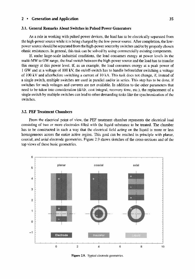
From the electrical point of view, the PEF treatment chamber represents the electrical loadconsisting of two or more electrodes filled with the liquid substance to be treated. The chamberhas to be constructed in such a way that the electrical field acting on the liquid is more or lesshomogeneous across the entire active region. This goal can be reached in principle with planar,coaxial, and axial electrode geometries. Figure 2.9 shows sketches of the cross-sections and of thetop views of these basic geometries.
6r-- - - ---,- - - - --.-- - - - --r-- - - - -.--- - - - r-- - - --,
5
4
3
2
o
-1
planar
o 2
coa xial
4 6
axial
8 10
Figure 2.9. Typicalelectrodegeometries.
36 Markus J. Loeffler
Planar electrode configurations consist of two parallel electrodes fixed by insulators. The insulators and the electrodes form a channel for the streaming liquid. Coaxial electrode configurationsconsist of two coaxial electrodes. The liquid streams between these electrodes that are fixed byinsulators not shown in the figure. Axial electrode configurations consist of several electrode ringson alternating potentials separated by insulating rings.
Planar electrode configurations ensure homogeneous fields provided their separation distanceis not significantly larger than their width. In the case of coaxial electrodes, the relation between theouter radius and the inner radius of the active zone should be smaller than 1.23 to ensure that theelectric field does not decay by more than 10%. To ensure homogeneous fields in the main treatmentzone of the axial electrode configurations, the direct proportionality of the electrode distance to thediameter of the channel should be maintained (Gaudreau et aI., 2004).
In addition to geometrical effects, the homogeneity of the electrical field also strongly dependson the permittivity and on the conductivity of the liquid. The separation distance of the electrodes isrestricted by the voltage available from the high-power supply. In commercial applications, voltageson the order of 100 kV are difficult to handle and, in many cases, offer a hard restriction. Forexponentially damped voltages, field requirements of "-'30 kV/cm lead to electrode gap separationsof "-'3 em. Another restriction is the amount ofpower available from the high-power source. Assuminga maximum power of P~ 1 GW ~ (e.g., this would relate to currents of "-'10 kA at voltages of"-'100 kV) and assuming a typical power density of p ~ 3 GW/L consumed by the liquid, the volumeof the active treatment zone would be restricted to
PV = - ~ 300mL.
p
For electrode separation distances of "-'3 em, the active area of the electrodes would be restrictedto "-'100 em".
An overview of some PEF treatment chambers investigated so far is given in (U.S. Food andDrug Administration, 2000). Actually, their volume is between 0.1 and 200 mL with electrode gapsbetween 0.1 and 1 cm.
Electrode materials also play an essential role. If monopolar voltage waveforms are applied,electrode corrosion can become critical and the substance to be treated can be contaminated. Incommercially available electroporation devices with small probes, aluminum, stainless steel, carbon,gold-plated electrodes, and even silver electrodes are used (Barbosa-Canovas et al., 2000; Puc et aI.,2004). Stainless steel electrodes suffer with problems such as electrolysis, formation of deposits,electrode corrosion, and transfer of particles into the treated media (Barbosa-Canovas et aI., 2000).Carbon electrodes are better for the inactivation of cells, since they have seemingly lower erosionrates, than stainless steel electrodes (Barbosa-Canovas et aI., 2000). Erosion can be minimized byapplying bipolar voltage waveforms (Johnstone and Bodger, 1997; Kotnik et al., 2001a).
3.3. High-Power Sources
Several methods exist for generating pulsed electric fields. Depending on the specified typeof voltage wave form, as well as on the available elements (capacitors, inductors, transformers,switches), the possibilities vary between simple circuits and very sophisticated networks. In thefollowing, several important possible pulsed power circuits will be discussed. The explanations arerestricted to the essentials. Practical devices, based on the circuits presented herein, are more complexdue to technical safety and failure handling necessities. There are also other possible schemes thatare driven by the physical and technical needs of the components, as well as that of the continuouslychanging ohmic properties of the load.
2 • Generation and Application
Figure 2.10. Capacitive circuit.
Basically, these circuits can be distinguished as being
• basic pulsed power circuits• circuits with voltage multipliers• pulse forming circuits or• networks with pulse forming switches.
3.3.1. Basic PulsedPower Circuits
3.3.1.1. Capacitive circuits
R
37
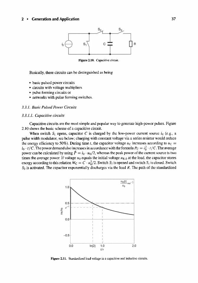
Capacitive circuits are the most simple and popular way to generate high-power pulses. Figure2.10 shows the basic scheme of a capacitive circuit.
When switch SI opens , capacitor C is charged by the low-power current source io (e.g., apulse width modulator, see below ; charging with constant voltage via a series resistor would reducethe energy efficiency to 50%). During time t, the capacitor voltage Uc increases according to Uc =io . t / C.The power demand also increases in accordance with the formula Pc = i5 . t/ C.The averagepower can be calculated by using j5 = io . uo/2, whereas the peak power of the current source is twotimes the average power. If voltage Uo equals the initial voltage UR.O at the load, the capacitor storesenergy according to this relation We = C . u~/2 . Switch Sz is opened and switch SI is closed. SwitchS3 is activated . The capacitor exponentially discharges via the load R. The path of the standardized
0.5- 1
o t'
~0::::J
1- - - - - - - 1- - -
11
UR lt) _ 1--=~ ,
Uo
0.0 ~------'----,----------l
- 0.5
0.0 10[2) 1.0ttr
2.0
Figure 2.11. Standardized load voltage in a capacitive and inductive circuits.

38
Figure 2.12. Inductive circuit.
R
Markus J. Loeffler
voltage uRluo across the load is shown in Fig. 2.11, where it plotted as a function of the normalizedtime t I r. The time constant T of the discharge circuit is defined by T = R . C. The voltage decaysto 50% of its initial value at t t t = In(2) ~ 0.693. At this time, the capacitor has delivered 75% ofits energy to the load. The capacitive power and energy at this moment have decreased to 25% of itsinitial value.
3.3.1.2. Inductive circuits
Figure 2.12 shows the basic scheme of an inductive circuit. After closing switch S\, the coilrepresented by its inductance L and resistance RL is charged by the low-power voltage source Uo
(e.g., bridge converter; charging with a constant current source would reduce the energy efficiency to50%) via switch S3. The coil current iL increases according to the formula ii. = Uo . (1 - e-8.t )1RL ,
where the coil's self-damping constant is 8 = RL/ L. When the working current io = uR.ol R, withinitial voltage UR.O at the load, is reached, the inductance stores an energy WL = L . i512. Switch SI isopened and switch S2 is closed (the inductance is "crowbared"). Switch S3 is opened, commutating thecurrent into the load. The inductance discharges exponentially via the load R. The path ofthe voltageacross the load is the same as that shown in Fig. 2.11. Here the time constant T of the circuit is definedby T = LI(R + RL ) . Again the voltage reaches 50% of its initial value at t f t = In(2) ~ 0.693. Asin the case of capacitive circuits, at this time the inductance has delivered 75% of its energy to theload and its own resistance and the power stored in the inductor has decreased to 25% of its initialvalue.
The inductor can also be charged by a charged capacitor instead of by the low-voltage sourceUo. In general, fast repetitive pulsed inductive circuits are not as effective as capacitive circuits. Thereason is that nonsuperconducting coils of reasonable shape have a power consuming resistance, thatdecreases the overall energetic efficiency of the process.
3.3.1.3. Ringing circuits
In addition to capacitive circuits, series and parallel ringing circuits are another simple andpopular way to generate high-power pulses. Figure 2.13 shows the basic diagram of a series circuit.
R
Figure 2.13. Serial ringing circuit.

2 • Generation and Application
1.0 a -+oo
0.5
0.0~~=-__-=~!!'ilII~ ~
- 0.5
39
0.0 In[2] 2.0lIT
4.0 6.0
Figure 2.14. Standardized load voltage in a serial ringing circuit.
A capacitor C is charged via a low-power current source io and the switches 5\ and 52 (compare tothe capacitive circuit).
If the capacitor reaches the voltage uo, switch 52 opens, switch 51 closes, and switch 53 isactivated. The capacitor discharges via the coil (L, Rd and the load R. The history of the normalizedload voltage is shown in Fig. 2.14 as function of the normalized time t f t , where r = (R + Rd· Cand a = (R + RdlL. Note that the formula given in the figure also holds for negative argumentsunder the root sign. The highest voltage can be achieved for a ~ 00 when the inductance L is small.In this case, the ringing circuit behaves like a capacitive circuit. The load peak voltage decreasessignificantly when a < 2.
Figure 2.15 shows the basic diagram of a parallel circuit. After opening switch 51, capacitor Cis charged by the low-power current source io. After reaching voltage uo, switch 52 opens, switch 5\closes, and switch 53 closes. The capacitor discharges via the inductance L, its resistivity RL,and theload R. The history of the normalized load voltage for RL « R is shown in Fig. 2.16, as a functionof the normalized time r = R . C and as function of a = 4 . R 2 . Cf L. The highest voltage can beachieved for a ~ 0 when the inductance L is very large. In this case, the ringing circuit behaves likea capacitive circuit. In practice, this behavior is maintained up to values a < 0.1.
Ringing circuits are less effective than capacitive circuits, either due to voltage reduction inthe inductor (series) or due to the reduction in time the voltage is maintained beyond the uol2 level(parallel).
R
Figure 2.15. Parallel ringing circuit.

40 Markus J. Loeffler
I
a=O.O0.5
1.0/ /4.0/8.0
0.5
URUI e-t, cos[~ 27 + a rc tan[~ ]]
1.0 U;= ~ 1 _.;
-0.5
0.0 In[2] 2.0tiT
4.0 6.0
Figure 2.16. Standardized load voltage in a parallel ringing circuit.
3.3.2. Circuits with Transformers or Other Voltage Multipliers
In the circuits discussed above, the on- and off-switches have to maintain a full load voltage(capacitive and inductive circuits); that is, the voltage across the capacitors (capacitive and ringingcircuits). At voltages above 100 kV and for repetition rates of ~1 Hz or more, the availability of highlifetime switches, as well as operation of the facilities become more and more critical. In this case,transformers or voltage multiplying circuits should be taken into consideration. In the following, coilswill only be represented by their inductances, assuming that their ohmic power losses are neglectablecompared to the energy input into the PEF load.
3.3.2.1. Circuits with pulse transformers
One way to multiply voltages is to use transformers that are switched between the high-powersource and the load. As an example, Fig. 2.17 shows the situation for capacitive circuits.
Capacitance C can be charged and discharged, as in capacitive circuits withouttransformer. If thewindings of the transformer, with inductances L] and L2, are coupled perfectly (where the mutualinductance between the windings is M ~ ~), the transformer amplifies the voltage by afactor of m ~ J L2/Lt. Because the discharge frequencies usually exceed 1 kHz, such transformersmust be either air core transformers or ferrite transformers. Looking backward from the load tothe capacitor, the circuit behaves like a parallel ringing circuit (Fig. 2.15), where inductance L
Figure 2.17. Capacitive circuit with pulse transformer.

2 • Generation and Application 41
II
... ,55\
III
R
Figure 2.18. Circuit with storage transformer.
is replaced with m2 • L, and the capacitance C is replaced with C/ m2 at the same voltage levelas the load. This circuit shows a nearly capacitive behavior, if a = 4· R2 . C/(m4
. L,) < 0.1 andif L2 = m2 . L, > 40· R2 . C[m", Compared to the capacitive circuit, the capacitance C and theon-switch S3 only have to achieve a voltage u-fm.
However, in real circuits with pulse transformers, the power consumed in the on-switch isslightly higher than in the capacitive circuits due to the unavoidable stray inductances and ohmicresistances in the pulse transformer. Furthermore, the additional pulse transformer increases thecost. Capacitive circuits with pulse transformers are only cost-effective, if the on-switches with therequired hold-off voltages are not available or, due to other technical problems, cannot be connectedin series. They also are financially practical if the current source is not able to deliver the chargingpower at the required voltage level.
3.3.2.2. Circuits with storage transformers
Figure 2.18 shows a circuit with a storage transformer and no capacitor. After closing switchS" the low-power voltage source Uo drives a current i, across the inductance L, of the transformer.Switch S3 is open, so that no current is induced in the secondary coil L2. The transformer behaves likean inductor L" so that the circuit behaves like an inductive circuit. After charging L, to the desiredcurrent level, S, is re-opened and switches S2 and S3 are closed. Assuming perfect magnetic couplingbetween the transformer windings (M =~) and after the powerless opening of switch S4,themagnetic flux and the energy of primary inductance L, transfers to the secondary inductance L2. Thecurrent across L2can be calculated by using i2 = i, . J L,/L2. Opening switch Ss commutates i2 intothe load, resulting in an initial load voltage UR = R . i2 • The circuit again behaves like an inductivecircuit with the time constant T = L2IR and with an exponentially damped current i: (Figs. 2.11and 2.12). When switch Ss is introduced into the circuit, the relationship between the primary andthe secondary inductance should be chosen so that L 2 « L, which means that the switches on theprimary side of the transformer can act at lower voltages, lower currents, and at lower power duringthe charging of L, and during switching at the end of the charge cycle.
In this scheme, the circuit has no advantage over inductive circuits, because switch Ss has toovertake the full voltage at the load. In principle, the circuit also works without this switch. Withoutswitch Ss, switch S4 would have to overtake the voltage US4 = J L I / L2 . U2. In this case, the primaryinductance, in order to act as a voltage multiplier, has to be essentially smaller than the secondaryinductance: L, « L2. Although this relieves the high voltage requirement for switch S4, it has to beconsidered that the overall switching power of this switch, at least, keeps the same value as that ofthe switching power of switch Ss in the preceding situation.
As in the case of capacitive circuits with pulse transformers, the transformer has stray inductances and ohmic resistance. Both increase the power requirements of the switches and of the voltagesource on the primary side of the transformer. With respect to high-voltage applications, PEF circuitswith storage transformers are less effective than inductive circuits.

42
Figure 2.19. MARX-generator (from Marx, 1923).
3.3.2.3. Voltage multiplier I (MARX-generator)
J
Markus J. Loeffler
The basic operating principles of the MARX-generator were first published by E. Marx in 1923(Marx, 1923). The original application of this voltage multiplying circuit was to test isolators and otherelectrical high-voltage devices. Figure 2.19 shows the original scheme. In two branches n capacitors Care connected in parallel via resistors W. Switches F connect the high potential and the low potentialterminals ofsuccessive capacitors (in this case spark gap switches). The ends ofthe capacitor branchesconnect to an isolator J (respectively, the load). The capacitors are charged by a current source viathe resistors to the same voltage. Igniting switches F connects the capacitors in series. By doing this,voltage multiplication occurs at the load. The resistors W discouple the capacitors if their resistanceis essentially higher than the (transient) resistance of the load. The overall capacitance dischargingvia the load is given by C/n. The resistors can also be replaced with opening switches if necessary.In this case, these switches have to open shortly before the switches F are ignited. After switching,the discharge behavior is equivalent to the discharge behavior of the capacitive circuit.
In MARX-generators, the on-switches have to maintain only lin of the voltage at the load.They have to conduct the load current. The low current source charging the capacitors only has todeliver 11n of the voltage than that required for the basic capacitive circuit at n times higher chargingcurrent. During charging, the overall capacitance of the capacitors switched in parallel has to be n2
times higher than in the capacitive circuit.As opposed to capacitive circuits, the capacitance and the main on-switch are divided into
several smaller switches and larger capacitances connected in series when system discharges. Theoverall volume, as well as the overall mass, of the capacitors will be slightly larger than that for basiccapacitive circuits when the same energy is to be stored in the capacitors due to added buswork. Theoverall switching power remains the same. As in the case with pulse transformers, MARX-generatorsshould only be chosen, if, with regard to the voltage requirements at the load, no adequate switchesand/or capacitors and/or current sources are available.

2 • Generation and Application
Jig_ C!. _
c c h;1~2_t C ~/1
r~C --i '- 1
Figure 2.20. Original GREINACHER cascade (from Greinacher. 1919).
3.3.2.4. Voltage multiplier II (GREINACHER cascade)
43
The GREINACHER cascade was invented by H. Greinacher in 1917 (Greinacher, 1919).Figure 2.20 shows a picture from the original source, whereas Fig. 2.21 shows its circuit diagram asit is used today. An AC-voltage source with a voltage amplitude u.: drives, via a charging resistorRCh, a column consisting of capacitors C and diodes D. After charging the capacitors via the diodesD, the n = 3 capacitors C on the right side are each charged to < 2 . Ii .: and are discharged in seriesvia a switch S to the load R. The resulting initial voltage on the load is <6· fL, with a resultingcapacitance of C/3. n modules, consisting of n capacitors and n diodes, provide an initial voltageUload < 2 · n . ic .: across the load at an overall capacitance C/n . The diodes in the circuit are driven atlow power, because they only have to overtake the charging current and double the voltage amplitudeat the voltage source . The main switch S has to handle the entire energy transfer at load powers . Theefficiency of Greinacher cascade s decreases with increasing number of stages due to the unavoidableohmic losses in the diode s that hinders charging each capacitor to 2 . U~ . From this point of view,MARX -generators provide higher efficiencies.
3.3.2.5. Current multiplier (XRAM-generator)
Publi shed by E. Marx and W. Koch in 1966 (Marx and Koch, 1970), Figure 2.22 shows theoriginal scheme, n coil s with inductance L 1 are connected in series via opening switches (2.2). Atthe ends of each inductor, closing switches (3) (in this case spark gaps) are connected. The inductorsare charged in series by the voltage source (2.1) to a current i \,0 . After reaching the desired current

44
D ' S
C
D
C
D
C R
D
C
D
C
D
C
u.
Figure 2.21. GREINACHER cascade.
Markus J. Loeffler
level, switches (2a) and (2.2) open and switches (3) close. By doing this, the inductors are switchedin parallel, generating an initial current i2,0 = n . il,o across the load (4). The current generates aninitial load voltage UR,O = n . R . i I,D, After switching, the discharge behavior is equivalent to thatof the basic inductive circuit.
3
3
:::L
II L,
n
4
Figure 2.22. XRAM-generator (from Marx and Koch, 1970).

2 • Generationand Application 45
In XRAM-generators, the opening switches have to maintain only lin of the current acrossthe load. However, they have to withstand the load voltage. The closing switches have to withstand:::::50% of the charge voltage at 1In of the current level at the load. The low-power voltage source,charging the inductances, has to deliver l in of the current required in the basic inductive circuit,but at n times higher charging voltage. During charging, the overall inductance of the single coilsswitched in series has to be n2 times greater than that of the inductive circuit. The overall volume, aswell as the overall mass, of the coils will comparable to the basic inductive circuits due to the sameamount of energy being stored in the coils for the same charging times. The necessity of repetitivesimultaneous switching of the off-switches causes problems that make the application of this typeof generator very difficult. Thus, XRAM-generators are not applicable to PEF applications.
3.3.3 . Pulse Forming Networks
Pulse forming networks allow the generation of monopolar or bipolar rectangular voltage waveforms preferred for PEF treatment applications.
The properties of pulse forming networks (PFNs) are based on the fundamental principlesof transmission lines. So, prior to an explanation of the electrical behavior of PFNs, the principalelectrical behavior of transmission lines will be briefly explained.
3.3.3.1. Pulse fanning lines
An ideallossless transmission line (or pulse forming line) may be represented by a coaxialcable of length I, inductance L = L' . I , and capacitance C = C' . I . Charging the capacitance of thistransmission line to a voltage Uo , or, respectively, to an energy We = C . u6/2, and discharging theline via a switch S into a load with resistance R = J LI C = JL'I C' generates a single rectangularvoltage pulse with amplitude uo/2and a duration of r = 2 .~ = 2 ·1 . "jErlc. £r is the relativepermittivity of the line's insulator and c is the velocity of light. Circuit diagrams of this circuit arepresented in the two pictures at the top of Fig. 2.23.
When the switch is triggered and if the line to the load is short-circuited at its other end, abipolar rectangular voltage waveform with amplitude ±uo/2 is generated, where each pulse has apulse length of r 12 (see Fig. 2.23, pictures in the center).
As a third possibility, the transmission line is split in two parts and a resistance 2·R reconnectsthe lines as seen in the bottom diagrams in Fig. 2.23. Short-circuiting the left end of the line generatesa rectangular voltage waveform of duration r 12 at a voltage amplitude Uo.
These examples show the flexibility of transmission lines with respect to the generation ofrectangular voltage waveforms. In all cases, the energy originally stored in the line's capacitance iscompletely transferred to the load. However, the following example will show the disadvantage ofthis solution.
With the following reasonable values
• load voltage UR .O = 100 kV• load resistance R = 10Q• pulse duration r ~ 15 I!S• pulse energy W = 5 kJ
the specification of the pulse forming line would be as described below.For a relative permittivity of £r ~ 3, the length of the line has to be I ~ 1.2 km. To store 5 kJ at a
voltage of 200 kV (only 50% of this voltage acts on the load), C' is calculated to be C' = 250 I!FIkm.

46 Markus J. Loeffler
1.5 ,.-- - - - - - - - - -,
1 ••_...••_••..•_•..•. _.•..._... . ._. ....~~.
I~ 0.51---------,'i
:l
-0.5
o 0.5 1.5Il r
1.5 ,-- - - - - - - - - ---,
--_._..._..._._.. ..__ .--..-- ..... _.--..~~.
Ia1--- --l----,.-- --i
-0.5
~ 0.51-----,'is
::>
L',C'.I, Ut ~
~---.-- ----- -.----- J R
o 0.5 1.5Il r
r----..., -....--..---.... - ~~.
L', C', 1{2, Uo L', C' , 1{2. Uo
~78--... --t::B-.--...(2·R
1.5
.._...
:! 0.51
0...::>
a
-0.5
0 0.5 1.5Il r
Figure 2.23. Pulse forming lines and voltage waveforms.
Conventional20-kV cables, like N(A)HKBA cables, have capacitances up to about 2 J.1.F/km (source:Felten & Guilleaume Energietechnik AG, Taschenbuch, 1995). The cables can withstand a peakvoltage of about 30 kYo So the ends of seven cables have to be switched in series, decreasing C' toabout 0.3 J.1.F/km. To reach 250 J.1.F/km, about 80 cable groups of seven would have to be switchedin parallel. Overall, such a device would result in the handling of 560 cables with a length of 1.2 km
47
L 1--------c
-------ll--------
2 • Generation and Application
L L L--------1 I I c Iuuu~J
c
Ic
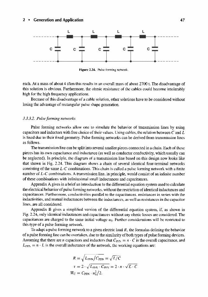
I IFigure 2.24. Pulse forming network.
each. At a mass of about 4 tJkm this results in an overall mass of about 2700 1. The disadvantage ofthis solution is obvious. Furthermore, the ohmic resistance of the cables could become intolerablyhigh for the high frequency applications.
Because of this disadvantage of a cable solution, other solutions have to be considered withoutlosing the advantage of rectangular pulse shape generation.
3.3.3.2. Pulse fanning networks
Pulse forming networks allow one to simulate the behavior of transmission lines by usingcapacitors and inductors with free choice of their values. Using cables, the relation between C and Lis fixed due to their fixed geometry. Pulse forming networks can bederived from transmis sion linesas follows.
The transmission line can be split into several smaller pieces connected in a chain . Each of thesepieces has its own capacitance and inductance (as well as conductor conductivity, which usually canbe neglected). In principle, the diagram of a transmission line based on this design now looks likethat shown in Fig. 2.24. This diagram shows a chain of several identical four-termin al network sconsisting of the same L-C combin ations. This chain is called a pulse forming network with a finitenumber of L-C combinations. A transmission line, in principle, would consist of an infinite numberof these combinations with infinitesimal small inductances and capacitances.
Appendix A gives in a brief an introduction to the differenti al equation system used to calculatethe electrical behavior of pulse forming networks, without the restriction of identical inductances andcapacitances. Furthermore, conductivities parallel to the cap acit ances, resistances in series with theinductivities, and mutual inductances between the inductances, as well as resistances in the capacitorlines, are all considered.
Appendix B gives a simplified version of the differential equation system, if, as shown inFig. 2.24, only identical inductances and capacitances without any ohmic losses are considered. Thecapacitances are charged to the same initial voltage U Q. Further considerations will be restricted tothis type of a pulse forming network .
To adapt a pulse forming network to a given electric load R , the formulas defining the behaviorof a pulse forming line can be overtaken , due to the similarity of both types of pulse forming devices.Assuming that there are n capacitors and inductors that CPFN = n . C is the overall capacitance, andLpFN = n . L is the overall inductance of the network , the working equations are:
R = .jLPFN /CPFN = J L / C
r = 2· J L pFN ' C PFN = 2 · n · J£. C
We = C PFN • uU2.

48
From these equations, L, C, and r can be calculated as
WeC=2--2n· Uo
2 WeL=2·R '--2
n· UoR· We
r=4·-u2o
Markus J. Loeffler
The pulse duration r is fixed by the values of R, uo, and We.Figure 2.25 shows some basic pulse forming networks, together with their voltage waveforms for
different numbers, n, of network elements. The networks differ slightly with respect to the switchesand to the transition from the network to the load. The networks in subfigures (a) and (b) simulatethe behavior of the pulse forming line shown in Fig. 2.23, top. Networks in subfigures (c) and (d)simulate the pulse forming line shown in Fig. 2.22, center. And the network in subfigure (e) relatesto the pulse forming line in Fig. 2.23, bottom. The calculation of the load voltage was performedby varying the number network elements between 1 and 10 (a-d), respectively, between 2 and14 (e).
The load voltage waveforms shown in Fig. 2.25 are normalized with the initial capacitancevoltage uo. The time is normalized with the time constant To The dashed lines represent the voltagebehavior of an ideal pulse forming line; that is, the behavior of a pulse forming network (PFN)with n --+ 00. The voltages in subfigure (a) are calculated by using the formulas given in AppendixB, whereas the voltages in subfigures (b)-(d), with to some minor modifications, are calculatedby using the formulas given in Appendix A. In all cases, the load resistance was chosen to beR = JL/C.
In detail the figures show:
Figure 2.25a: Initially, switch S2 is opened and the current source io charges the n capacitorsC via the inductors L. After charging is completed, switch S, is opened and switch S2 isclosed. Closing switch S3 initiates discharge via the load R.
For n = 1, the network represents a well-damped ringing circuit with the respective loadvoltage (light-gray curve). Increasing n leads more and more to an approximation of thevoltage waveform of a pulse forming line (dashed curve; compare to Fig. 2.23, top). Thevoltage keeps at about 50% of the initial voltage of the capacitors.
Figure 2.25b: The PFN differs from the PFN in Fig. 2.25a by the lack of an inductance betweenthe last capacitor and the load. Charging and initialization of the discharge is the same aswith the previous network.
For n = 1, the network represents a capacitive circuit with a respective load voltage (lightgray curve). The fact that the voltage does not yield the capacitance's initial voltage is due toa small inductance between the capacitance and the load, which is not shown in the diagram,but is included the calculation. Increasing n leads more and more to an approximation of thevoltage waveform of a pulse forming line (dashed curve). Beside the unavoidable voltagepeak at the beginning, the voltage remains at about 50% of the initial voltage of the capacitorsnearly throughout the entire pulse duration.
Figure 2.25c: Initially, SI is open and the current source io charges the n capacitors C via theinductors L. After charging is completed, switches S, and S2 are closed simultaneously toinitiate discharge via the load R.

2 • Generation and Application 49
For n = 1, the load voltage is ringing (light-gray curve). Increasing n leads more and moreto an approximation of the bipolar rectangular voltage waveform of a pulse forming lineshort-circuited at one end (dashed curve; compare to Fig. 2.23, center). The voltage amplitudekeeps at about 50% of the initial voltage of the capacitances. The ringing period is r ,
Figure 2.25d: The PFN differs from the PFN in Fig. 2.25c due to the lack of an inductancebetween the last capacitance and the load. Charging and initialization of the discharge is thesame as that with the previous network.
(a)
1/ = I ... 10
1/ = I : light-gray curve
1/ =10: black curve
1.0
R
S, L L L
...----r-L-r---j- - - --.--c e - e - cT -/,
- 0.5
0.0 0 .5 1.0 1.5II'
(b)
1/ = I ... 10 1.0
1/ = I : light-gray curve
black curve0.5
1/ = 10:oS
s, L L L S, J-----[JI 00
I. e= c=_____~_= RI- 0.5
0.0 0.2 0.4 0.6 0.8 1.0 1.2 1.4II'
(c)
1/ = I ... 10
1/ = I: light-gray curve
1/ = 10: black curve
1.0
I, R
II·
Figure 2.25. Basic pulse forming networks and related load voltage waveforms.
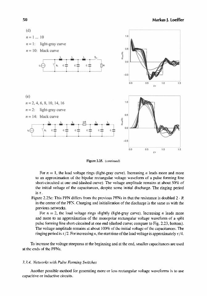
50 Markus J. Loeffler
(d)
/I = I ... 10 1.0
Lr---r-.-~~-. - - ~ - - j
Ie - e - R
L---+._-+- '- - --l
/I = I : light-gray curve
/I =10: black curve
1/ ,
L
1-- - --1e - e -
~-_<~_+_--+- J
L L L 2,R-- --- II, e= e- e=
(e)
/1 =2,4,6,8,10, 14,16
/I = 2: light-gray curve
/I = 14: black curve
- 0,5
0,0 0,5 1,0 1.5
Figure 2.25. (continued)
For n = 1, the load voltage rings (light-gray curve). Increasing n leads more and moreto an approximation of the bipolar rectangular voltage waveform of a pulse forming lineshort-circuited at one end (dashed curve). The voltage amplitude remains at about 50% ofthe initial voltage of the capacitances, despite some initial discharge. The ringing periodIS To
Figure 2.25e: This PFN differs from the previous PFNs in that the resistance is doubled 2 . Rin the center of the PFN. Charging and initialization of the discharge is the same as with theprevious networks.
For n = 2, the load voltage rings slightly (light-gray curve). Increasing n leads moreand more to an approximation of the monopolar rectangular voltage waveform of a splitpulse forming line short-circuited at one end (dashed curve; compare to Fig. 2.23, bottom).The voltage amplitude remains at about 100% of the initial voltage of the capacitances. Theringing period is T /2. For increasing n, the start time of the load voltage is approximately T /4.
To increase the voltage steepness at the beginning and at the end, smaller capacitances are usedat the ends of the PFNs.
3.3.4. Networks with Pulse Forming Switches
Another possible method for generating more or less rectangular voltage waveforms is to usecapacitive or inductive circuits.
2 • Generation and Application 51
Load(processing unit)
Lseries
Lseries
Solidstateswitch(120 kV, 750 A peak)
Rseries
1 IlF
Cstorage
Cstorage
Solidstate switch(120kV, 750 A peak)
Rseries
Solidstatepower
supplies
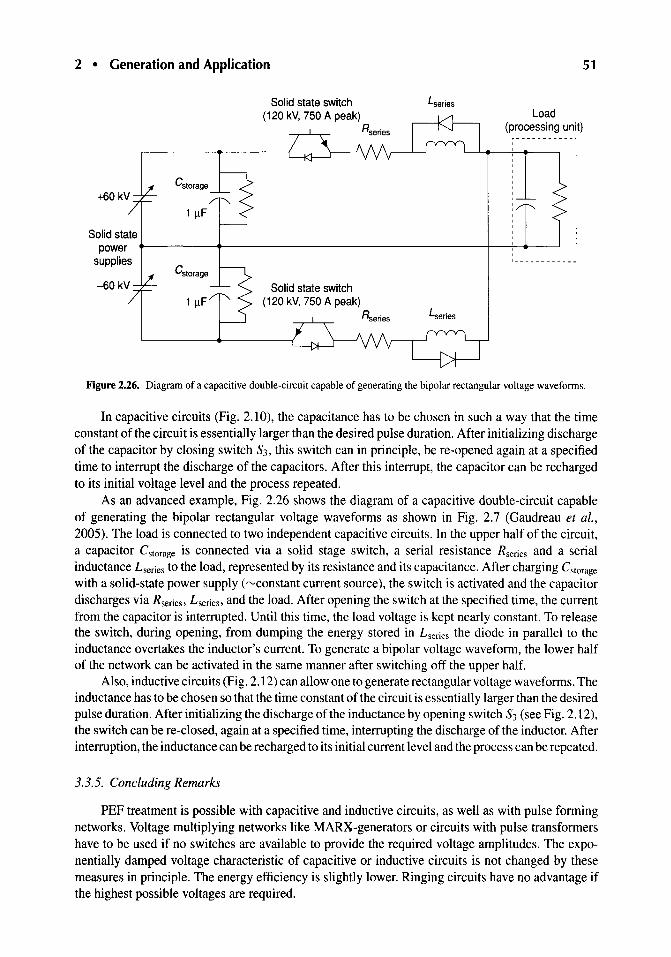
Figure 2.26. Diagram of a capacitive double-circuit capable of generating the bipolar rectangular voltage waveforms.
In capacitive circuits (Fig. 2.10), the capacitance has to be chosen in such a way that the timeconstant of the circuit is essentially larger than the desired pulse duration. After initializing dischargeof the capacitor by closing switch 53, this switch can in principle, be re-opened again at a specifiedtime to interrupt the discharge of the capacitors. After this interrupt, the capacitor can be rechargedto its initial voltage level and the process repeated.
As an advanced example, Fig. 2.26 shows the diagram of a capacitive double-circuit capableof generating the bipolar rectangular voltage waveforms as shown in Fig. 2.7 (Gaudreau et al.,2005). The load is connected to two independent capacitive circuits. In the upper half of the circuit,a capacitor Cstorage is connected via a solid stage switch, a serial resistance Rseries and a serialinductance Lseries to the load, represented by its resistance and its capacitance. After charging Cstorage
with a solid-state power supply (r-constant current source), the switch is activated and the capacitordischarges via Rseries, Lseries, and the load. After opening the switch at the specified time, the currentfrom the capacitor is interrupted. Until this time, the load voltage is kept nearly constant. To releasethe switch, during opening, from dumping the energy stored in Lserics the diode in parallel to theinductance overtakes the inductor's current. To generate a bipolar voltage waveform, the lower halfof the network can be activated in the same manner after switching off the upper half.
Also, inductive circuits (Fig. 2.12) can allow one to generate rectangular voltage waveforms. Theinductance has to be chosen so that the time constant of the circuit is essentially larger than the desiredpulse duration. After initializing the discharge of the inductance by opening switch 53(see Fig. 2.12),the switch can be re-closed, again at a specified time, interrupting the discharge of the inductor. Afterinterruption, the inductance can be recharged to its initial current level and the process can be repeated.
3.3.5. Concluding Remarks
PEF treatment is possible with capacitive and inductive circuits, as well as with pulse formingnetworks. Voltage multiplying networks like MARX-generators or circuits with pulse transformershave to be used if no switches are available to provide the required voltage amplitudes. The exponentially damped voltage characteristic of capacitive or inductive circuits is not changed by thesemeasures in principle. The energy efficiency is slightly lower. Ringing circuits have no advantage ifthe highest possible voltages are required.

52 Markus J. Loeffler
Rectangular voltage waveforms can be generated by either applying pulse forming networks orcapacitive or inductive circuits with "oversized" time constants and with switches that are able tointerrupt the current across the load at a specified time.
In all networks or circuits, the overall power demand of the switches remains independent ofthe number and the arrangement of the switches as well as the type of circuit. The same is true for
the energy content of the capacitors or inductors.
3.4. Components of HighPower Sources
The main components of high-power sources are storage capacitors and on- and off-switches.
Because of their relatively high ohmic power consumption, inductors in comparison to capacitorsplaya minor role.
Depending on the application, different capacitor types with different specific prices are on themarket. One of the main requirements of capacitors is a long lifetime at the specified voltage andenergy content. Based on a common design, the construction of different types of capacitors dependson the discharge current.
Many variants of fast switches are available: spark gaps, electron tubes (thyratrons), and semiconducting switches (diodes, thyristors). Depending on the technical specifications, these switcheshave specific merits and limitations. Mechanical switches are too slow for high repetition rate PEF
generation.
3.4.1. High-Power Capacitors
In principle high-power capacitors consist of a couple of thin sandwich-like metallic-dielectricmetallic-dielectric strips of "-'100 urn thickness. The dielectrics are made, for example, from Kraftpaper, polypropylene, mixtures of Kraft paper with polypropylene, or PVDF. The electrodes aremade from aluminum, either as a foil or sprayed onto the dielectric. Each sandwich strip is rolledup. The resulting windings are flattened. Each flat winding represents an elementary capacitor. Theycan be switched in series or in parallel to construct the final capacitor. Further information about theconstruction of capacitors is given in MacDougall (1996).
Together with some basic data about commercially available capacitors, Fig. 2.27-1 lists somedifferent types of capacitors of different sizes in metallic or in plastic casings.
Figure 2.27-2, left, top, gives an overview of the range of voltage and capacitance of capacitorsprovided by a large capacitor supplier (Ennis et al., 2003). At voltages of about 1 kV, the highestcapacitances are nearly 100 mF, whereas at voltages in the MV range the capacitances have valuesin the 100-pF range. The figure shows that, in general, the realized capacitance of single capacitorshas smaller values at higher voltages.
Figure 2.27-2, right, top, gives an overview of the range of energy densities and design lifeof capacitors (Ennis et al., 2003). For a design life of about 1000 charge/discharge cycles, energydensities up to about 2 kl/L were achieved. To achieve very high lifetimes, that is, on the order of
1013 charge/discharge cycles, the energy density has to be reduced to about 0.1 kl/L, Increasing thelifetime of capacitors is possible by decreasing the energy stored per unit volume. The lifetime ofcapacitors also depends on other factors like voltage, dielectric stress, voltage reversal, stressed areaof the dielectric, and ringing frequency (Smith et al., 2004): "A traditional power scaling guidelinehas been used by capacitor manufacturers to predict actual component lifetimes based on knownsensitivities to these important parameters. One of its most general forms is given by
L = La. (~) -4. (El~])-3.5. (gJ -1.6. (:J- 1/P
. (~) -0.5

2 • Generation and Application
• capacitance:
• voltage:
• energy:
• lifetime:• specific cost:
up to -0.1 F
up to -MV
<2.5 kJ/Lup to _1014 cld cycles
>0.05 US$/J
53
Figure2.27-1. Capacitors. Left: different types of capacitors (source: Maxwell Laboratories Inc.), right: general data (taken
from Fig. 2.26-2).
~
== 10'g
.~
"[10 '.."
10' .--,--.,---,---,-----,.--,
lri'
~ 10-' 1-- +--'~
.~:; 10" f--j- - I'."
~~ 10- 3 1--+--+--+-+-''---t~1-l
10 • I--- ,-- f-
10-5 '-:--"-:---'---...i...:'---'-,--'-::::----'-:."...---'lri' 1 ~ 10' 10" 10" 10'0 10" 10"
design life IC/O cyclesI
10-2 '-;--"-;--"-;--"-;--"-:---'-:---'.,.,.- """'--'10' lOS lOe 107 10& 109 10' 0 1011 10' 2
design life (C/O cycles]
~VJ 10'2ino"o!t
8....
10'" 10"energy (kJI
lit'efiN".
Figure2.27-2. Typical data of capacitors; Left, top: voltage and capacitance (MacDougall, 1996); right, top: range of energydensity and rated voltage (MacDougall, 1996); left. bottom: relative cost per Joule versus life of different high energy capacitortechnologies; right, bottom: specific cost versus energy (Maxwell Laboratories Inc.lAMS Electronic GmbH, 1997).
54 Markus J. Loeffler
In this expression, L represents the expected short life after scaling; V is the capacitor operatingterminal voltage; E is the dielectric electric field stress; A is the stressed dielectric area of theoperating unit; f3 is the Weibull slope or shape factor; f is the ringing frequency of the operatingunit; Q = (n /2)/ In(1/R) is the operating circuit quality factor; and R is the actual operating reversal(%). The symbols La, Va, Eo, Ao, fa, Ro, and Qo are the baseline rated design parameters." Theexponents in the scaling law vary depending on the materials used. Increasing/decreasing each ofthese parameters compared to the baseline-rated parameters decreases/increases the expected lifetimeof capacitors remarkably.
Figure 2.27-2, left, bottom, shows the relation between the relative cost per Joule and the designlife. The curves relate to different types of materials and technologies:
1. self-healing metallized electrodes, Kraft paper with film2. self-healing metallized electrodes, metallized film dielectrics, high-resistance electrode3. combined metallized electrodes with foil electrodes4. self-healing metallized electrodes, metallized film dielectrics, segmented electrode5. extended foil electrodes/tabbed foil; "single-shot," up to 100 kV, up to 1 MA, more than 20%
voltage reversal; paper dielectric/mixed dielectric/all-film combined metallized electrodeswith foil electrodes.
"Hybrid electrode," types 3 and 6, are especially useful in long-life industrial applications, suchas water and food sterilization. In the case of type 5, a cost increase by a factor of ~6 can be expectedif the design life increases by a factor of ~106.
Figure 2.27-2, right, bottom, shows the specific cost of capacitors relative to the stored energyfor different capacitors in general and for different lifetimes (price base: year 1997). As a general rule,the specific cost decreases with increasing energy. At energies of "'-100 kJ/capacitor, the decrease inthe cost reaches its minimum at "'-0.05 US$/J.
3.4.2. Switches
The following specific high-power switches will now be taken into consideration below:
1. Trigatrons (three-electrode spark gaps)2. Ignitrons3. Thyratrons and pseudospark switches4. Thyristors and IGCTs.
In the following, some typical electrical values of the respective switches will be given.
3.4.2.1. Trigatrons
Trigatrons or spark gaps are the workhorse in laboratories. In principle, they consist of twoelectrodes with an additional trigger electrode between the main electrodes or implemented intoone of the electrodes. The gap between the electrodes is filled with air, synthetic air, sulfur hexafluoride, SF6-Argon, or oxygen-argon at different pressures ranging down to vacuum pressures.Because of their simple construction, trigatrons are cheap if no demands are imposed on theirlifetimes.
Figure 2.28-1 shows a selection of trigatrons of different size for different purposes togetherwith some fundamental data.
Figure 2.28-2, left, top, shows the typical operating voltage and peak current ranges and, onthe right, top, peak powers and energy transfer rates that can be handled by trigatrons in single-shot

• peak current:• voltage:• energy:• peak power:• lifetime:• specific cost:
up to -MAup to - 500 kV<3 MJ/pu\se<0.4 TVAup to _109 discharges>400US$/GYA
Figure 2.28-1. Trigatrons. Left: different types of trigatrons (source : Maxwell Laboratories Inc.); right: general data (takenfrom Fig. 2.28-2).
* c.NJ. lI B.• • wo. en..
• CAlli0 C0 Cu
~ '" Cu- tb,.o. 0 IU
~o. • 6.
• • o.
• o. t -o. ." o.L>
b 0
:(~c.. 0.1§o~
III
8-0.01
loS
en lOT..:; loSs:o~ Hi
.§ 10'
~llY
Hi
5 10 50 100voltage [kV\
10' Hipeak curren t (kA]
,.~..III 0.1:;Co
8-0.01
~III<:g
0.001>-!!'..<:..
0.0001
0.000015001000 0.001
llY
0.1 10peak power IGVA\
10-2 10-1 100peak power [GVA \
1000
10'
Figure 2.28-2. Typical data of trigatrons. Left. top: range of trigatron voltage and peak current; right, top: range of trigatronenergy transfer and peak power; left, bottom: peak current and lifetime expectancies (from (Donaldson, 1990), modified);right, bottom: peak power and specific cost (source: Richardson Electrics Ltd., 2005).
56 Markus J. Loeffler
operation. Trigatrons can work at voltages up to "-'500 kV, at peak currents up to "-'3 MA, at peakpowersup to "-'300GVA, andatenergytransferratesup to "-'2 MJ/discharge. Here,as in thefollowingsections, the peak poweris definedto be the productof the hold-offvoltageand the peak current.Thepeak currentsdecrease to 10--30% as the repetitionrate increases(up to 100Hz). Nonetheless, thesevaluesare impressive and imply that trigatronscan be used for nearlyanyon-switch tasks in pulsedpower technology. The drawback is the relatively short trigatron lifetime of "-'106 discharge cyclesat currents of 10 kA or more (Fig. 2.28-2, left, bottom). At repetition rates of "-' 10 Hz, the lifetimeis on the order of only "-'30 h, thus hinderingthe industrialapplications for trigatrons. The prices oftrigatronsare shownin Fig. 2.28-2, right, bottom. In addition, the price of trigger generators has tobe taken into account with prices of about 3-4 thousandUS$ per single switch (source: RichardsonElectronicsInc., 2005).
3.4.2.2. Ignitrons
Ignitronsconsistof an anode (usuallygraphite)and a mercurypool cathode.A semiconductingtrigger electrode which dips into the mercury pool cathode and initiates the discharge. An electronemitting source is formed at the point where the trigger contacts the pool. This initiates an arcingbetween the anode and the cathode. As long as there is a significant current flow, the ignitron willremainconducting. Continuously operatingignitronsmustbe cooled to a well-defined temperatures.Ignitronsmust be placed in a verticalposition so that the mercurypool is in the right position in thetube.
Figure 2.29-1 showsan ignitronwith a surroundingcoolingcoil togetherwith some basic data.Figure 2.29-2, left, top, shows typical trigger voltage and peak current data for a ignitron.
Ignitrons can withstand voltages up to 50 kV and peak currents up to 700 kA. They can switchpeak powersup to "-' 10GVA (Fig. 2.29-2, right, top). The averagepower, shownin Fig. 2.29-2, left,bottom, is on the order of 0.1% of the peak power. The specific power cost of ignitrons decreaseswith increasingswitchingpower. They vary between 400 and 2000 US$IGVA peak power.
Although, in general, ignitrons do not cause trouble, they have an increasing negative imagedue to the mercury inside the ignitrons. For the most applications, they can be replaced by otherswitchdevices, so their use should be avoidedwhen possible.
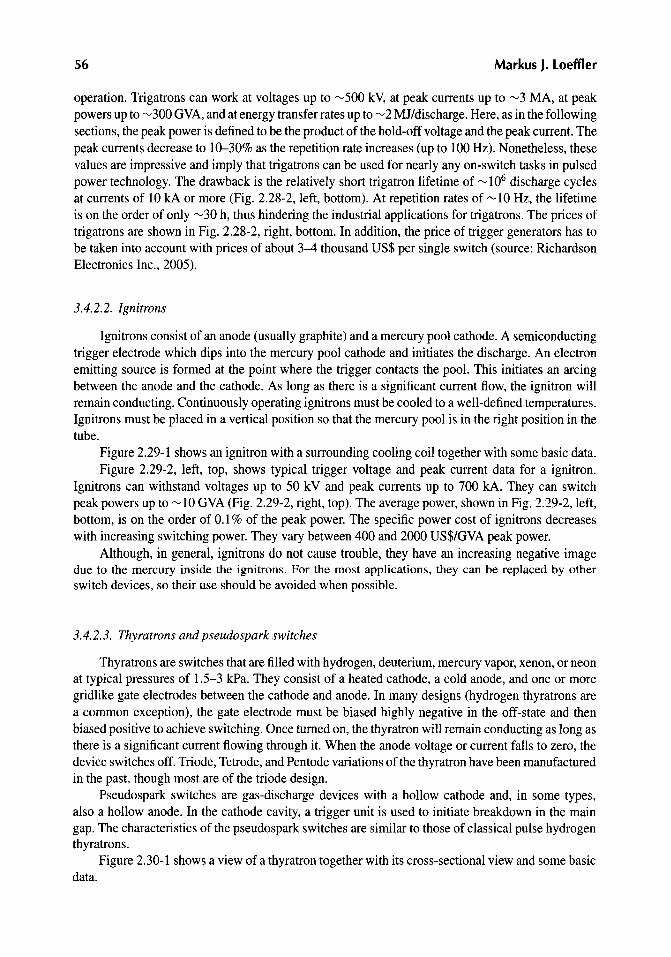
3.4.2.3. Thyratrons and pseudospark switches
Thyratrons are switchesthat are filledwithhydrogen, deuterium, mercuryvapor, xenon,or neonat typical pressures of 1.5-3 kPa. They consist of a heated cathode, a cold anode, and one or moregridlike gate electrodes between the cathode and anode. In many designs (hydrogen thyratrons area common exception), the gate electrode must be biased highly negative in the off-state and thenbiasedpositiveto achieveswitching. Once turnedon, the thyratronwill remainconductingas long asthere is a significant current flowing through it. When the anode voltageor current falls to zero, thedeviceswitchesoff.Triode,Tetrode, andPentodevariations of the thyratronhavebeenmanufacturedin the past, though most are of the triode design.
Pseudospark switches are gas-discharge devices with a hollow cathode and, in some types,also a hollow anode. In the cathode cavity, a trigger unit is used to initiate breakdownin the maingap.The characteristics of the pseudospark switchesare similar to those of classicalpulsehydrogenthyratrons.
Figure 2.30-1 showsa viewof a thyratrontogetherwith its cross-sectional viewand somebasicdata.

2 • Generation and Application 57
• peak current:• voltage:• average power:• peak power:• specific cost:
:5:700 leA:5:50kV<IMVA<IOGVA>400 US$/GVA
Figure 2.29-1. Ignitrons. Left: ignitron; right: general data (taken from Fig. 2.29-2).
1000
500
~ 200
20
-I
I •I -•
- -- -, •I" ,
I
• ••
10
5
~ 2
G;:=a
.><
'"8. 0.5
0 .2
- - :I• •
•-• •- --
•
1010 15 20 30 50 70 100
voltage IkVI
0.110 15 20 30 50 70 100
voltage IkVI
~ 100
1000
500
3000.2
f-- •
•
.-- •• •
20100.5 1 2 5peak power [GVA j
3000
500
2000
;;ou
~ 700'u..c-O'
~ 1500Q...so21000
1.5 2 3 5 7 10 15 20peak power IGVAI
I • -•
J-I- -I • I,
• , ,I
I
I I
II I
50
10
5
~a'"'"'"G;>
'"
Figure 2.29-2. Typical data of ignitrons. Left. top: Voltage and peak current; right. top: voltage and peak power; left, bottom:peak power and average power; right, bottom: peak power and specific cost (source: Richardson Electronis Ltd., 2005)
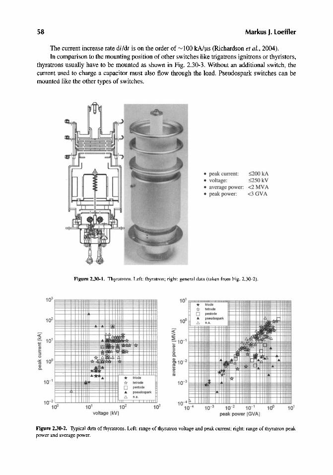
Figure 2.30-2, left, shows typical ranges of thyratron voltage and peak current data. Thyratronsand pseudospark switches can handle voltages up to ""200 kV and peak currents up to ""200 kA.These switches allow energy transfers with peak powers up to ""2 GVA and average powers up to""I MVA (Fig. 2.30-2, right).
58 Markus J. Loeffler
The current increase rate di/dt is on the order of '"100 kA/llS (Richardson et al., 2004).In comparison to the mounting position of other switches like trigatrons ignitrons or thyristors,
thyratrons usually have to be mounted as shown in Fig. 2.30-3. Without an additional switch, thecurrent used to charge a capacitor must also flow through the load. Pseudo spark switches can bemounted like the other types of switches.
• peak curre nt:• voltage :• average power:• peak power:
$200 kA$250 kV<2 MVA<3GVA
Figure 2.30-1. Thyratrons. Left: thyratron; right: general data (taken from Fig. 2.30-2).
103 101
1<i 100
~<'>
10' ~1O- ''E coe ;::; au.:.: 10° 8,10-2coa '"iii
>co1-10-1I~rodt
pontoclopslW:lolp arkn.e.
10-2 10-' I100 101 102 103 10-' 10-2 10- ' 10'
voltage [kVI peak power [GVAI
Figure 2.30-2. Typical data of thyratrons. Left: range of thyratron voltage and peak current; right: range of thyratron peakpower and average power.

2 • Generation and Application
C
)------+----1 t--o
Thyratron
Thyristor
c
59
Figure 2.30-3. Mounting position of thyratrons compared to thyristors or other switches.
The average lifetime of thyratrons is on the order of 11/2 for 3 years of continuous operation(Richardson et al., 2004; Welleman et al., 2004). A thyratron system that operates at a voltage of9 kV, a pulse current of 2.5 kA, a pulse length of 10 I-!S, a dUdt of 5 kAl1-!S, and a pulse repetitionrate of 400 Hz usually costs 4000 US$, whereas the tube itself costs 2300 US$ (Welleman et al.,2004).
3.4.2.4. Thyristors, diodes, and IGCT switches
In principle, thyristors (=thyratron + transistor) are four-layer semiconducting devices, witheach layer consisting of an alternately N- or P-endowed material, for example, N-P-N-P. The outerlayers represent the cathode (N) and the anode (P). The control terminal, or "gate," is attached toone of the middle layers. After ignition, thyristors remain conducting as long as the current does notreverse. Some thyristors are optically triggered.
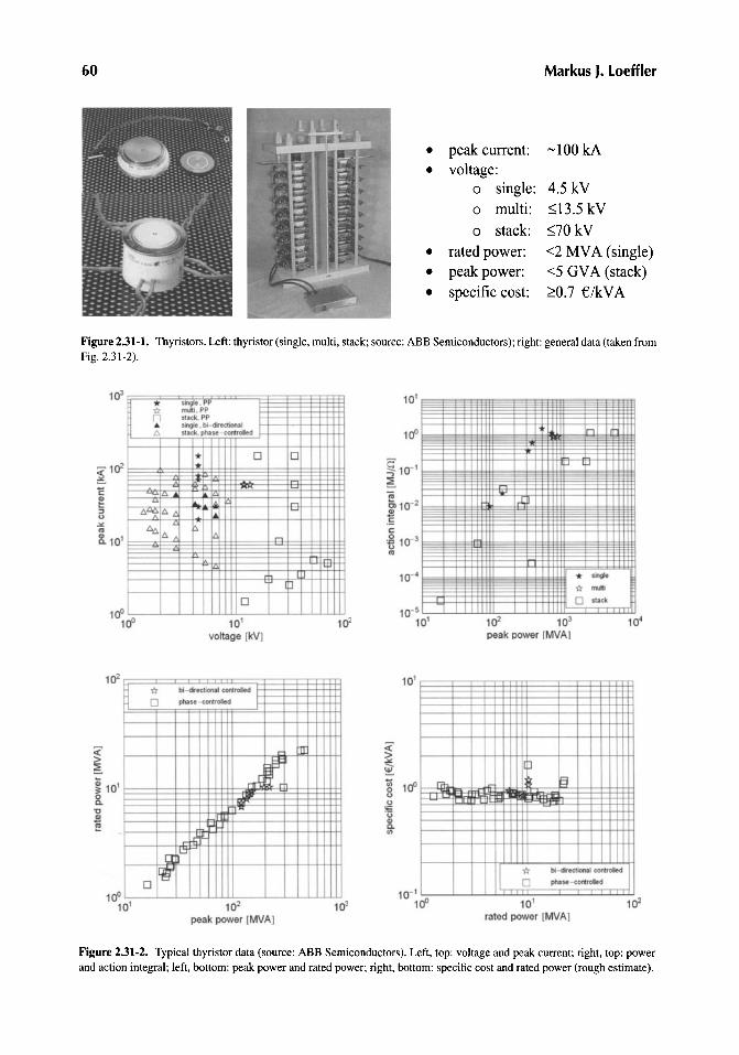
Figure 2.31-1 shows some types of thyristors with either a single semiconducting wafer in aceramic housing, multiple wafers in a ceramic housing, or combined in a stack. Their key parametersare also given.
Figure 2.31-2 shows some typical characteristics of single thyristor disks, multi-layer thyristors,and stacked thyristors. Single thyristor disks can be stressed by voltages of 4.5 kV at peak currentsup to more than 100 kA (Fig. 2.31-2, left, top). Multi-layer thyristors can be stressed by voltages of~ 15 kV at peak currents up to 50 kA, whereas thyristor stacks are available for voltages up to 70 kVand for peak currents up to more than 100 kA. Note that for continuous operation, the currents andthe power are a factor of 10-20 less than the peak currents and the peak powers, respectively.
The action integral
A = 100
i2dt ,
which is proportional to the energy deposit in the thyristor and the load during one discharge atpeak current, can reach values up to ~l MJ/Q at power levels up to 5 GVA (Fig. 2.31-2, right,top) for a single-shot. Current increase rates dUdt are limited to ~20 kAll-!s. Repetition rates can
60 Markus J. Loeffler
• peak current: ~100 kA
• voltage:0 single: 4.5 kV
0 multi: $13.5 kV
0 stack: $70kV
• rated power: <2 MVA (single)
• peak power: <5 GVA (stack)
• specific cost: :?O.7 €/kVA
Figure 2.31-1. Thyristors. Left: thyristor (single. multi, stack; source: ABB Semiconductors); right: general data (taken fromFig. 2.31-2).
,I .nLJ rtilllJ
I II Iii-' CJiitHffi-
I ~ I II-
J. ,
- * ..0« """0 \.tack
I II I I
.,:I~pp~n stack. PP r f-I-.. ... bI·dlre<t.....1
l:> Jlack. phue -cortr*d
* 0 01<
-
~
"';. I ~
l:>~ l:> /J I I ~
".
~A C.
::::::::::=:..
,'J
0
10'voltage [kVI
10'
100
l eY 103
peak power [MVAJ10'
leY10'rated power [MVA]
.J ImI
E~
:::0: - ,I I
I
II
III0« bi-drect ional cortrolM
0 phaM - corcroll'd
1
10'
loJ102
peak power [MVAj
~~ bl~OrKhonal conlrohd
0 phil,. - ( odroled
J hr l
~~
~I!-
I--If0 I
leY
Figure 2.31-2. Typical thyristor data (source: ABB Semiconductors). Left, top: voltage and peak current; right, top: powerand action integral; left, bottom: peak power and rated power; right, bottom: specific cost and rated power (rough estimate).
2 • Generation and Application 61
be up to 100 Hz at rated power. Typical values of the rated power (or average power) normalizedby the peak power are shown in Fig. 2.31-2, left, bottom. As shown in Fig. 2.31-2, right, bottom,the specific cost of thyristors (single) are in the range of 0.7-1.5 €lkVA rated power. For continuous operation, the lifetime of thyristors is on the order of 10 years and more (Welleman et al.,2004).
At a voltage of 9 kV, a pulse current of 2.5 kA, a pulse length of 10 IlS, a di/dt of 5 kNlls, anda pulse repetition rate of 400 Hz, the typical cost of a thyristor stack is 8700 US$ (Welleman et al.,2004).
Thyristors switch-off if the current reverses, but are not able to switch-off the current beforezeroing. Integrated Gate Controlled Thyristors (IGCT) have the capability to switch-off currents actively. As the IGCT is the improved version of GTOs (Gate Turn-Off Thyristor), the GTO technologyis not used anymore for pulsed applications (Welleman et al., 2004). Although their turn-on behaviorand di/dt is reduced compared to the discharge switches mentioned earlier, they offer the possibilityto drive circuits with pulse forming switches. Single GTO switches are designed to switch-on and toswitch-off currents up to 4 kA. Blocking voltage per device is 4.5 kV or 6 kv. They are usually usedin medium- and high-power drivers and frequency converters. The switches can be stacked so that,with a reverse blocking IGCT device consisting of seven 4.5-kV IGCTs, forward/reverse blockingvoltages of 31 kV at nominal 1600-lls pulse currents of 2.5 kA can be switched at repetition rates of15 Hz (Welleman et al., 2004). Frequencies up to 400 Hz are possible.
As a perspective optically triggered Emitter Turn-Off Thyristors (ETO) can operate at currentsup to 4 kA and at voltages of 6 kV at frequencies of more than 1 kHz with less power consumption.The maximum current increase rate di/dt is 1 kNIlS.
Diodes are passive switches, that switch on automatically at negative voltages. Figure 2.32, left,shows the peak current and voltage of several types of diodes with a single wafer. Peak currents upto 90 kA can be switched for blocking voltages up to 6 kv. The rated power over the peak power isshown in Fig. 2.32, right. The rated power (average power) has values up to 25 MVA at peak powerlevels up to 400 MVA. As a rule of thumb, the specific power cost of diodes relative to their averagepower can be estimated as 3/4 of the cost of comparable thyristors.
'* '*'*a-
D ~..ii... A
;::;... ........ -
~
'" wekU1g'-
0 fJ~ ' KOV«)' I... \I.nd.lrdrecO'tel)'
I10°
voltage IkVj
102* wolck>g
0 fu t recOVfl)'
... standilrd recO'/eryI 1.0.c--
I -r>'...
...,. ... I
... ~ I
I10' 102
peak power [MVA JloJ
Figure 2.32. Typical data of diodes (source: ABB Semiconductors). Left: voltage and peak current; right: peak power andoperational power.

62
3.4.2.5. Concluding remarks
Markus J. Loeffler
For PEF applications, thyratrons and semiconducting switches offer the most promising possibilities. Trigatrons suffer from relatively short lifetimes, whereas ignitrons are more and more out offavor due to the mercury inside the tube. The choice between thyristors and thyratrons depends onthe specific requirements of the load. At voltages of r- 100 kY, there are clear advantages for usingthyratrons, especially with respect to the investment cost. At voltages lower than 30 kY, thyristorswitches may yield lower operation cost than thyristors due to their comparably higher lifetime.
3.5. Low-Power Source
3.5.1. Basic Considerations
The low-power source (AC/DC converters) converts an alternating voltage into a constantcurrent, constant voltage, or constant power to charge the capacitors or inductors of the highpower source. The term "low power" means low power compared to the power of the high-powersources. Several types of such converters exist. Their technical details are discussed, for example, in[48]. Figure 2.33 shows typical values of the power and output frequencies of commercially available converters (Brosch et al., 2000). Power levels up to '"100 MYA have been realized in largefacilities.
In high repetition rate circuits, like PEF circuits, the converter is the most expansive part. Thecost depends on the maximum current and the maximum voltage, which defines the rated power ofthe device, that the converter can handle. For cost-effectiveness, the power utilization factor shouldbe as high as possible to achieve high energetic efficiency.
It is well known that the charging of capacitors with constant voltage via a resistor yieldsan energetic efficiency of not more than 50% and a power utilization not more than 25%.On the other hand, charging with constant currents yields energetic efficiencies of more than90% at comparably high-power utilization factors. Charging with constant power is in between
102 103 10~
operation frequency 1Hz]
Figure 2.33. Converters. range of frequency and power (from (Brosch et ai., 2000, Mitsubishi), modified in the low frequencyregion with values from ABB Semiconductors).

2 • Generation andApplication 63
these two types. From this, it clearly turns out that capacitors should be charged by a constant currentsource.
For constant charging current io, the power in the capacitor is
Pc = Uc . io.
The capacitor voltage increases according to the following formula
ioUc = -. t,
C
so that the power can be calculated with
·210
Pc = C· t.
The power increases linearly with time. If the charging voltage Uo is attained, the peak powerat the capacitor is
Pc = Uo . io.
This power, plus some additional power to account for ohmic losses, has to be installed in theconstant current power supply. The minimum cost of this device can be calculated by applying therule of thumb that define the specific cost to be 0.5 €/W.
The average power is half the peak power. So, as an example, a device with an average power of300 kW (compare Fig. 2.6) would need an installed power of 600 kW. The cost would be in minimum300k€.
3.5.2. Typical Devices
To close this chapter, some typical systems that have already been constructed and that are inuse will be briefly described.
Figure 2.34 shows a power supply for PEF applications that allows one to charge capacitorsup to 18 kV at an average power of 35 kJ/s and at repetition rates up to 100 Hz. On the left side ofthe figure, the power supply is shown as a customer usually sees it. The cost of a device is about
Figure 2.34. 35 kJ/s/l8 kV power supply (source: BARMAG, Propuls).

64 Markus J. Loeffler
storage vessel
water line
manual control
automatic control •••
power supply
mains (230/400 V)~
-.
2.0m
2.1 m
cable
-a m
Figure 2.35. 20 kJ/s120 kV monopolar solid-state PEF pulser (source: AMS ElectronicslPropuls).
30 k€ according to the specific cost per unit power estimate given above. Doubling the power wouldincrease the cost by ~50% (Neumann, 1. personal communication, 2005).
Figure 2.35 shows a solid-state pulser delivering monopolar exponentially damped pulse voltages of 20 kv, The 50-Hz pulser has an average power demand of 20 kW. Its purpose is the treatmentof potatoes with PEF for the starch industry (see Fig. 2.35, top). The potatoes are positioned by asteady flow of water between two electrodes. After the PEF treatment, a conveyor screw transportsthe potatoes to the next stage where the softened potatoes are treated mechanically. A low-voltagepower and the electronic controls are located on the left side of the pulser (see Fig. 2.35 right, bottom).

2 • Generation and Application 65
Figure 2.36. 75 kJ/s/60 kV bipolar solid-state PEF pulser (Gaudreau et aI., 2004, 2005) (source: Diversified Technologies).
A 20-kJ/s average power supply is positioned below a capacitor and a solid-state switch part on theright side. The cost of the complete system was about 150 k€.
Figure 2.36 shows a solid-state PEF pulser with an average power of 75 kJ/s (Jin et aI., 2002;Gaudreau et al., 2004, 2005). Its high-power circuit is shown in Fig. 2.26. The pulser generatesbipolar or monopolar square waveform voltages with 60 kV amplitude at currents up to 750 A. Thepulse repetition rate is between 500 and 2000 pps. The pulse width varies between 2 and 8 us. Eachpulse delivers 10-100 J of energy. The system is nominally sized to process orange juice at a rate of2000 L/h. For highly resistive foods, like apple juice, the unit can process up to 5000 L/h. The totalcost of the system, including pulse generator, aseptic drink processing unit, PEF treatment chamberunit, and aseptic packaging machine, was about 700 k€.
APPENDIX A: DIFFERENTIAL EQUATION SYSTEM OF INHOMOGENEOUSPULSE FORMING NETWORKS
Figure A-I shows the most generalized form of a pulse forming network replacing pulse forminglines. Different admittances Ck II Gk connected in parallel are connected with different resistances Wk
and with switches S in serial. Different impedances Li-R; are connected in series. The capacitancesCi are charged to different charging voltages Uk,D. Switches S simultaneously switch on and initiatea current via the load R. The n2 - n mutual inductances Mk,l between the single inductances arerepresented by the collective letter M.
To define the linear differential equation system of the circuit the following matrices and vectorsare introduced:

66 Markus J. Loeffler
m
,.---I...- --+--__u-----.t--I...- -..- - .-J- --..--l~}__-----,
s s
G3 II
.-- .......-~~-.......- ---41>--+_- _+ - -- ..--- .......- ---41>-- - - - - ----1
Figure A·1. Inhomogeneous pulse forming network
Matrix ofcapacitances:
C1 0 0 0 00 C2 0 0 00 0 C3 0 0
c=
0 0 0 Co-1 00 0 0 0 Co
i-Matrix:
1 0 0 0 0 0-1 1 0 0 0 00 -1 1 0 0 0
E=
0 0 0 -1 1 00 0 0 0 -1 1
Matrix of conductivities:
G1 0 0 0 00 G2 0 0 00 0 G3 0 0
G=
0 0 0 GO- 1 00 0 0 0 Go
R

2 • Generation and Application
Matrix of inductances and mutual inductances:
67
LI M1,2 M1,3M1,2 Lz MZ,3M1,3 MZ,3 L3
L=
MI,n-1 MZ,n-1 MZ,n-1MI,n Mz,n M3,n
Matrix ofZeroes (n x n-matrix):
0 0 00 0 00 0 0
0=
0 0 00 0 0
Ml,n-lMZ,n-1M3,n-1
Mn-I,n-IMn,n-l
o 0o 0o 0
o 0o 0
Matrix of resistances:
-(WI + RI + W2 ) W2 0 0 0W2 -(W2 + R2 + W3) W3 0 0
0 W3 -(W3 + R3 + W4 ) 0 0w=
0 0 0 -(Wn- 1 + Rn- I + Wn ) Wn
0 0 0 Wn -(R+ Rn)
Vector ofcapacitance voltages and initial capacitance voltages:
UI [t] UI,OUz [t] UZ,OU3 [t] u3,O
U [t] = uo =
Un-I [t] Un-I,OUn lrl Un,O
Vector of inductance currents and initial inductance currents:
il [t] 0iz [t1 0h [t] 0
I [t] = io =
in-I [t] 0in [t] 0
Applying these matrices and vectors the differential equation system is defined with:

68
with the block matrices
and
and with the block vectors
and
d 1-v[t] = A- . B· v[t], v[O] = Vodt
A= (~ ~)
- (-9 -E)B- £T W
(U[t ])
v[t] = i[t]
Markus J. Loeffler
APPENDIX B: DIFFERENTIAL EQUATION SYSTEM DESCRIBINGHOMOGENEOUS PULSE FORMING NETWORKS
Figure B-1 shows the most popular form of a pulse forming network. Here all capacitances andinductances are identical: C, = C, L, = L. Resistances Rk and Wb conductivities Gk and mutualinductances Mk,l are neglected. The initial capacity voltages are now identical: Uk,O = Uo. Hence theswitches S now can be combined in a single switch at the load R.
To define the linear differential equation system of the circuit the matrices and vectors of theinhomogeneous pulse forming network can be simplified as follows:
Matrix ofcapacitances:
C1 0 0 0 00 C2 0 0 00 0 C3 0 0
C=
0 0 0 Cn- 1 00 0 0 0 Cn
l~~~-lco/
L2 L3 Ln S
R
1-------Figure B-t. Homogeneous pulse forming network without losses.

2 • Generation and Application
I-Matrix:
1 0 0 0 0 0-1 1 0 0 0 00 - 1 1 0 0 0
E =
0 0 0 - 1 1 00 0 0 0 -1 1
Matrix of inductances:
L, 0 0 0 00 L2 0 0 00 0 L3 0 0
L=
0 0 0 0 00 0 0 0 Ln
Matrix ofZeroes (n x n-matrix):
0 0 0 0 00 0 0 0 00 0 0 0 0
0=
0 0 0 0 00 0 0 0 0
Matrix of resistances:
0 0 0 0 00 0 0 0 00 0 0 0 0
w=
0 0 0 0 00 0 0 0 -R
69

70 Markus J. Loeffler
Vector of capacitance voltages and initial capacitance voltages:
Ul [t] UoU2 [t] UoU3 [t] Uo
U [t] = Uo =
Un-l [t] UoUn [t] Uo
Vector of inductance currents and initial inductance currents:
i1 [t] 0i2 [t] 0i3 [t] 0
I [t] = io =
in- 1 [t] 0in [t] 0
Applying these matrices and vectors the differential equation system is defined with:
d 1-V[t] = A- . B· V[t], V[O] = Vodt
with the block matrices
A _ (C 0)- 0 .c
and
and with the block vectors
(u[t ])
vlrl = i[t]
and
ACKNOWLEDGMENT
The author of this chapter would like to express his thanks to Dr. Larry Altgilbers who significantly improved the readability of the text.

2 • Generation and Application
REFERENCES
71
Barbosa-Canovas, G. v., Pierson, M. D., Zhang, Q. H., and Schaffner, D. W, 2000, Pulsed electric fields, 1. Food Sci. 65(8):65-79.
Bazhal, M. I., 2001, Etude du mecanisme d'electropermeabilisation des tissus vegetux. Application ii l'extraction du jus des
pommes, These de Doctorat, Universite de Technologie de Compiegne, France.Bodecker, v., 1985, Zum Technologiepotential der Plasmaphysik (About the Technological Potential of Plasma Physics),
VDI-Verlag, DUsseldorf.Brosch, P. E, Landrath, J., and Wehberg, J., 2000, Leistungselektronik, Braunschweig, Wiesbaden, VIEWEG Verlag.Donaldson, A. L., 1990, Lifetime considerations, In: Gas Discharge Closing Switches (G. Schaefer, M. Kristiansen, and A.
Guenther, eds.), Plenum Press, New York, pp. 325-344.Ennis, J. B., Song, B. M., Bushnell, A. H., Cooper, R. A., Jichetti, J., MacDougall, E, McDowell, R., Andermatt, B., and
Bates, J., 2003, Custom design of components and power supplies for pulsed power systems, General Atomics EnergyProducts, Engineering Bulletin, Presented at IEEE Industrial Electronics Conference (IECON 2003).
Gaudreau, M. P. J., Hawkey, T, Petry, J., and Kempkes, M., 2004, Design considerations for pulsed electric field processing,In: Proceedings of2nd European Pulsed Power Symposium, Hamburg, Germany, pp. 58-61.
Gaudreau, M. P.J., Hawkey, T., Petry, J., and Kempkes, M., 2005, Pulsed Power Systemsfor Food and Wastewater Processing,Diversified Technologies, Bedford, MA, www.divtecs.com.
Greinacher, H., 1919, Hochspannungsanlage zur Erzeugung von hochgespanntem Gleichstrom aus Wechselstrom unter Verwendung von elektrolytischen Ventilzellen und Kondensatoren, Swiss Patent No. 80289.
Heinz, v., Alvarez, I., Angersbach, A., and Knorr, D., 2002, Preservation of liquid foods by high intensity pulsed electricfields-basic concepts for process design, Trends Food Sci. Techno!. 12: 103-111.
Heinz, v., Angersbach, A., and Knorr, D., 2001, Membrane permeabilization in biological materials in response to pulsedelectric fields-a highly efficient process for biotechnology, In: Proceedings of International Conference on PulsedPower Applications, Gelsenkirchen, Germany, pp. B.03/1-B.0317.
Heinz, v., ToepfI, S., and Knorr, D., 2003, Impact of temperature on lethality and energy efficiency of apple juice pasteurizationby pulsed electric fields treatment, Innov. Food Sci. Emerg. Techno!. 4(2.2): 167-175.
Jemai, A. B., and Vorobiev, W, 2002, Effect of moderate electric field pulse (MFEP) on the diffusion coefficient of solublesubstances from apple slices, Int. J. Food Sci. Techno!. 37: 73-86.
Jin, Z. T, and Zhang Q. H., 2002, Commercial scale integrated PEF processing system and its operation cost, 2002 1FTTechnical Paper Presentation 91E-21.
Johnstone, P. T, and Bodger, P. S., 1997, High voltage disinfection of liquids, IPENZ Trans. 24: 30-35.Kotnik, T, Miklavcic, D., and Mir, L. M., 2001a, Cell membrane electropermeabilization by symmetrical bipolar rectangular
pulses: Part II. Reduced electrolytic contamination, Bioelectrochemistry 54: 91-95.Kotnik, T., Mir, L. M., Flisar, K., Puc, M., and Miklavcic, D., 200 Ib, Cell membrane electropermeabilization by symmetrical
bipolar rectangular pulses: Part I. Increased efficiency of permeabilization, Bioelectrochemistry 54: 83-90.Kotnik, T, Pucihar, G., Rebersek, M., Miklavcic, D., and Mir, L. M., 2003, Role of pulse shape in cell membrane electrop
ermeabilization. Biochim. Biophys. Acta 1614: 193-200.Lazarenko, B. R., Fursov, S. P., Scheglov, Y. A., Bordiyan, V. v., and Chebanu, V. G., 1977, Electroplasmolysis, Karta
Moldovenaske, Kishinev.Loeffler, M., Schmidt, W., Schuhmann, R., Rottering, A., Neumann, J., and Dreesen C; 2001, Treatment of sewage
sludge with pulsed electric fields, In: Proceedings of International Conference on Pulsed Power Applications,Gelsenkirchen.
MacDougall, E W., 1996, Capacitors for the pulsed power industry, Technical Paper Aerovox Div. PPC, 167 John VertenteBoulevard, New Bedford, MA 02745-1221.
Marx, E., 1923, Verfahren zur Schlagpriifung von Isolatoren und anderen elektrischen Vorrichtungen, German PatentNo. 455933, 12.
Marx, E., and Koch, W, 1970, Induktiver StoBstromgenerator, Offenlegungsschrift 1488941, Deutsches Patentamt, 19.McLellan, M. R., Kime, R. L., and Lind, L. R., 1991, Electroplasmolysis and other treatments to improve apple juice yield,
J. Sci. Food Agric. 57: 77-90.Min, S., Jin, Z. T, Min, S. K., Yeom, H., and Zhang, Q. H, 2003a, Commercial-scale pulsed electric field processing of orange
juice,J. Food Sci. 68: 1265-1271.Min, S., Min, S. K., and Zhang, Q. H., 2003b, Inactivation kinetics of tomato juice lipoxygenase by pulsed electric fields, 1.
Food Sci. 68: 1995-2001.Ngadi, M., Bazhal, M., and Raghavan, G. S. v., 2003, Engineering aspects of pulsed electroplasmolysis of vegetable tissues,
Agric. Eng. Int. 5: 1-10.

72 Markus J. Loeffler
Papchenko, A. Y, Bologa, M. K., and Berzoi, S. E., 1988a, Apparatus for processing vegetable raw material, US PatentNo. 4787303.
Papchenko,A. Y., Bologa, M. K., Berzoi, S. E., Paukov, 1. N., Rudkovskaya, G. v., and Chebanu,V.G., 1988b,Electroplasmolyzer for processing vegetablestock, US Patent No. 4723483.
Puc,M., Corovic,S., Flisar,K.,Petkovsek,M., Nastran,J., and Miklavcic,D., 2004,Techniquesof signalgenerationrequiredfor electropenneabilization.Surveyof electropenneabilizationdevices,Bioelectrochemistry 64: 113-124.
Qin, B. L., Zhang, Q., Barbosa-Canovas, G. v.. Swanson, B., and Pedrow, P. D., 1994, Inactivation of microorganisms bypulsed electric fieldof different voltage waveforms, IEEE Trans. Dielectr. Insul. 1: 1047-1057.
Reitler,W, 1990, Conductive heating offoods, PhD Thesis, TU Munich,Munich.Richardson,B., Pirrie,c.,Clarke, K., and Dunlop,A., 2004,Thyratronor solid state? Switchingtechnologyoptions for pulse
powerapplications.In: Proceedings of2nd European Pulsed Power Symposium, Hamburg,pp. 8-13.San Martin, M. E, Barbosa-Canovas, G. v., and Swanson, B. G., 2003, Innovations in Food Processing, CEP
(www.cepmaganzine.org), March, pp. 54-60.Smith,D. L., Savage,M. E., Ziska, G. R., and Starnbird,R. L, 2004,ZR MARXcapacitorlifetimetest results, In Proceedings
of the 2004 Power Modulator Conference, San Francisco, CA, May 2004 (paper number P-HPG&HCL I-I).Toepfl, S., Heinz, v., and Knorr, D., 2004, Optimizationof pulsed electric field treatment for liquid food pasteurization,In:
Proceedings of2nd European Pulsed Power Symposium, Hamburg,Germany, pp. 68-72.Ulmer, H. M., Heinz, v., Ganzle, M. G., Knorr, D., and Vogel, R. E, 2002, Effects of pulsed electric fieldson inactivation
and metabolicactivityof Lactobacillus plantarum in model beer,J. Appl. Microbiol. 92: 326-335.U.S. Food and Drug Administration 2000, Center for Food Safety and Applied Nutrition:Kineticsof Microbial Inactivation
for AlternativeFood ProcessingTechnologies; Pulsed Electric Fields. June 2.Weise,Th. H. G. G., and Loeffler, M. J., 2001, Overviewon pulsed powerapplications, In: Proceedings of the International
Conference on Pulsed Power Applications, Gelsenkirchen,Germany,pp. A.0I/I-A.01/8.Welleman, A.,Fleischmann,W, andWaldmeyer, J., 2004,Solidstateswitchesforrepetitivepulseapplications.In: Proceedings
of 2nd European Pulsed Power Symposium, Hamburg,pp. 176-180.Zhang, Q., Barbosa-Canovas, G. v., and Swanson,B. G., 1995,Engineeringaspects of pulsed electric fieldpasteurization,1.
Food Eng. 25: 261-281.