GENERAL DESCRIPTION packages. FEATURES - 2.6V to 5.5V operating input voltage range - Adjustable...
16
TOP BEST IC CO., LTD. TB3050 1 / 16 Version: 1.0 2013.01.03 680K/1.2MHZ, HIGH VOLTAGE, BOOST CONVERTER GENERAL DESCRIPTION The TB3050 is a high performance, high efficiency step up DC-DC Converter with integrated 3A. The TB3050 converter input voltage ranging from 2.6 to 5.5V. The Output voltage can be set up to 27V. The selectable frequency of 680 kHz and 1.2 MHz allows the use of small external inductors and capacitors and provides fast transient response. Current mode control with external compensation network makes it easy to stabilize the system and keep maximum flexibility. Programmable soft start function minimizes impact on the input power system. Internal power MOSFET with very low RDS (ON) provides high efficiency. The TB3050 automatically transits from PWM to PFM during light load condition further increasing efficiency. The converter also provides protection functions such as Current Limit and Thermal shutdown. The TB3050 is available in space-saving MSOP-10L-EP, MOSP-8L-EP, TDFN-10L and SOP-8L-EP packages. FEATURES - 2.6V to 5.5V operating input voltage range - Adjustable output voltage range up to 27V - Up to 3A output switch current - 680K/1.2MHz Selectable Switching Frequency - Programmable soft-start function - External Compensation Network - Current limit and Thermal shutdown protection - Under voltage Lockout - ≤ 1μA Shutdown Current - Available in the Pb-Free MSOP-10L-EP, MSOP-8L-EP ,TDFN-10L and SOP-8L-EP Packages
Transcript of GENERAL DESCRIPTION packages. FEATURES - 2.6V to 5.5V operating input voltage range - Adjustable...
TOP BEST IC CO., LTD. TB3050
1 / 16 Version: 1.0 2013.01.03
680K/1.2MHZ, HIGH VOLTAGE, BOOST CONVERTER
GENERAL DESCRIPTION
The TB3050 is a high performance, high efficiency step up DC-DC Converter with integrated
3A. The TB3050 converter input voltage ranging from 2.6 to 5.5V. The Output voltage can be
set up to 27V. The selectable frequency of 680 kHz and 1.2 MHz allows the use of small
external inductors and capacitors and provides fast transient response. Current mode control
with external compensation network makes it easy to stabilize the system and keep maximum
flexibility. Programmable soft start function minimizes impact on the input power system.
Internal power MOSFET with very low RDS (ON) provides high efficiency. The TB3050
automatically transits from PWM to PFM during light load condition further increasing efficiency.
The converter also provides protection functions such as Current Limit and Thermal shutdown.
The TB3050 is available in space-saving MSOP-10L-EP, MOSP-8L-EP, TDFN-10L and
SOP-8L-EP packages.
FEATURES
- 2.6V to 5.5V operating input voltage range
- Adjustable output voltage range up to 27V
- Up to 3A output switch current
- 680K/1.2MHz Selectable Switching Frequency
- Programmable soft-start function
- External Compensation Network
- Current limit and Thermal shutdown protection
- Under voltage Lockout
- ≤ 1µA Shutdown Current
- Available in the Pb-Free MSOP-10L-EP, MSOP-8L-EP ,TDFN-10L and SOP-8L-EP
Packages

TOP BEST IC CO., LTD. TB3050
2 / 16 Version: 1.0 2013.01.03
BLOCK DIAGRAM
VCC
SS
LX
SGND
Control and Driver Logic
EN
COMP
1.238V Reference
Soft Start
Current Sense
Slope Compensation
Oscillator
FB
Error Amplifier
Summing Comparator
Thermal Shutdown
7uA
Enable/ Disable
PGND
N-MOS
FREQ
PIN ASSIGNMENT
The packages of TB3050 are MSOP-10L-EP, TDFN-10L, SOP-8L-EP and MSOP-8L-EP;
the pin assignment is given by:
( Top view )
MSOP-10L-EP
LX
SGND
VCC
COMP
PGND
SS
FREQ
EN
1
2
3
4
5 6
7
8
9
10
FB
LX
Exposed Pad
(SGND)
( Top View )
1
2
3
4
8
7
6
5
EN
GND
SOP/MSOP-8L-EP
AX5913
COMP
FB
SS
FREQ
LX
VCC
ExposedPad
(GND)
TDFN-10L (3*3)
COMP
LX
1
PGND
10
2
3
4
5 6
7
8
9FB
EN
SGND
LX
VCC
FREQ
SS
Exposed
Pad(SGND)
TOP View
Name Description
VCC Power Input pin
EN Enable Pin
COMP Compensation Pin
FB Feedback Pin
SS Soft start Pin. Connect a capacitor to GND
GND Ground Pin
SGND Signal Ground
PGND Power Ground
LX Switch Output Pin
FREQ
Frequency select pin. The power switch operates at 680kHz if FREQ is connected to GND and at 1.2MHz if FREQ is connected to VCC

TOP BEST IC CO., LTD. TB3050
3 / 16 Version: 1.0 2013.01.03
ORDER/MARKING INFORMATION
Order Information
TB3050 XXX X
Package Type PackingBlank : TubeA: TapingEU: MSOP-10L-EP
J10: TDFN-10L (3*3)
ES: SOP-8L-EP
EU8: MSOP-8L-EP
Top Marking (MSOP/SOP) Top Marking (TDFN)
Logo
YTB 3 Part number
ID code:internal
WW:01~52
Year: 10=2010
11=2011
0 5 0Y WWX
3 Part number
ID code: internal
WW: 01~52
Year: 10=2010
11=2011
Y Y W WX
0 5 0
ABSOLUTE MAXIMUM RATINGS (at TA=25°C)
Characteristics Symbol Rating Unit
VCC Pin Voltage VCC GND - 0.3 to GND + 6 V
EN, FREQ,COMP,FB,SS, Pin Voltage GND - 0.3 to VCC + 0.3 V
LX Pin Voltage VLX 30 V
Power Dissipation PD ( TJ-TA ) / θJA mW
Storage Temperature Range TST -65 to +150 °C
Operating Junction Temperature Range TOP -40 to +125 °C
Thermal Resistance from Junction
to case
MSOP-8/10L-EP
θJC
30
°C/W TDFN-10L 20
SOP-8L-EP 15
Thermal Resistance from Junction
to ambient
MSOP-8/10L-EP
θJA
80
°C/W TDFN-10L 55
SOP-8L-EP 40
Note: θJA is measured with the PCB copper area of approximately 1.5 in2(Multi-layer). That copper area needs connect to exposed pad.

TOP BEST IC CO., LTD. TB3050
4 / 16 Version: 1.0 2013.01.03
ELECTRICAL CHARACTERISTICS
(VIN=5V, VOUT=12V, VEN=VIN, TA=25°C, unless otherwise noted)
Characteristics Symbol Conditions Min Typ Max Units
Input Voltage range VCC 2.6 - 5.5 V
Under Voltage Lockout UVLO Rising - 2.35 2.6 V
UVLO Hysteresis - -150 - mV
Step-Up Voltage Adjust Range VOUT VCC+0.5 - 27 V
Operating quiescent current ICCQ IOUT= 0mA, VFB=1.5V - 150 250 μA
Shutdown current ISD VEN=0V - 0.1 1 μA
Feedback Voltage VFB 1.219 1.238 1.257 V
FB Input Leakage Current IFB-LKG VFB = 1.5V -100 0.01 +100 nA
Line Regulation VIN=2.6 to 5.5V IOUT=20mA
- 0.2 - %
Load Regulation VIN=5V IOUT= 1mA to 0.7A
- 0.3 - %
Oscillator frequency FOSC FREQ=High 900 1200 1500
KHz FREQ=Low 500 680 850
FREQ high-level input voltage VFQ-IH 2 - - V
FREQ low-level input voltage VFQ-IL - - 0.5
FREQ input leakage current IFQ-LKG FREQ=GND - - 0.1 uA
Soft Start Current ISS 4 7 13 μA
N-channel MOSFET current limit ILIM Duty=40% 3 3.8 4.5 A
MOSFET on-resistance
(Note1) RDS(on)
VIN=3V, ISW=2A - 200 280 mΩ
VIN=5V, ISW=2A - 160 220
EN high-level input voltage VIH 1.0 - - V
EN low-level input voltage VIL - - 0.4 V
EN Hysteresis hys - 200 - mV
EN input leakage current IEN-LKG VEN=GND or VIN - 0.01 0.1 μA
Maximum Duty Cycle Duty VFB=0V 85 90 - %
LX Leakage Current ILXL VLX = 25V, VFB=1.5V - - 10 µA
Thermal Shutdown TDS - 150 - °C
Thermal Shutdown Hysteresis TSH - 35 -
Note:Guaranteed by design.
TOP BEST IC CO., LTD. TB3050
5 / 16 Version: 1.0 2013.01.03
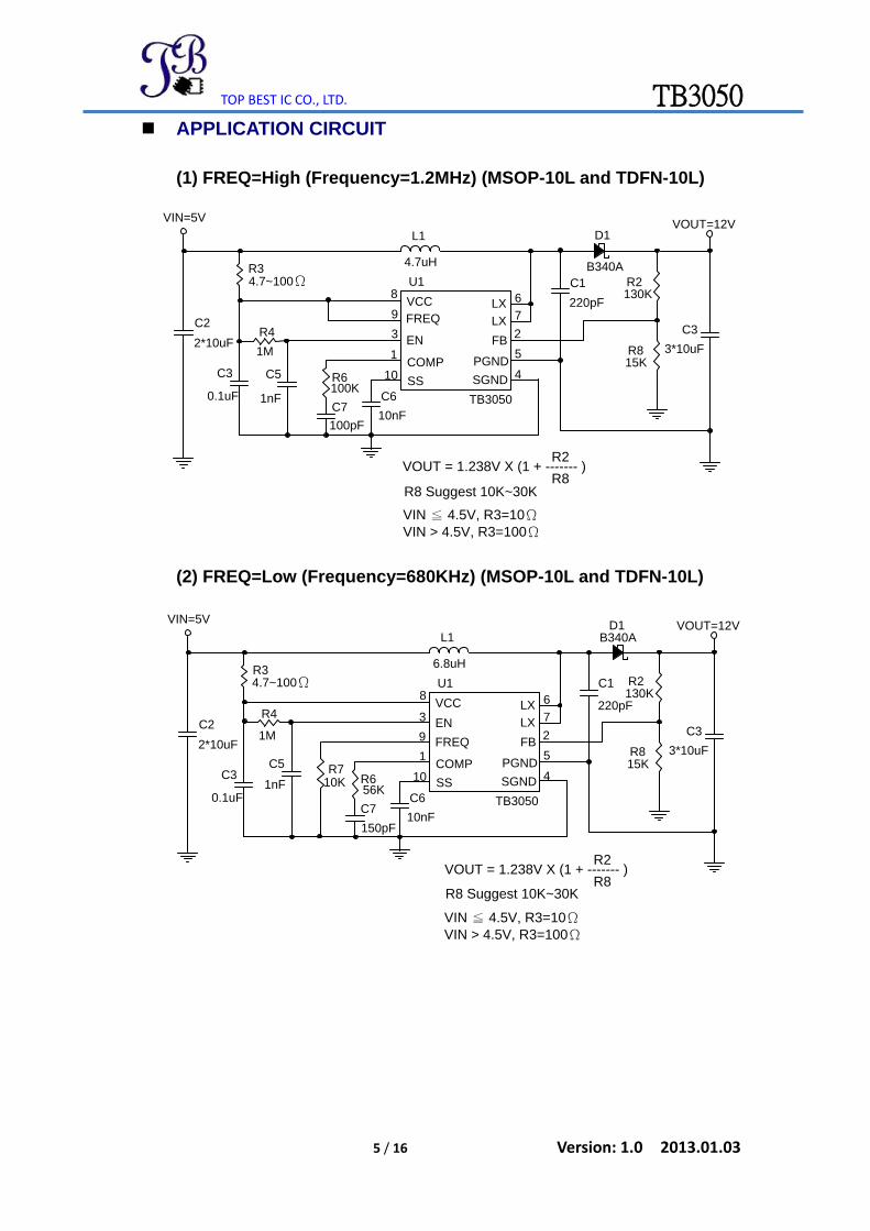
APPLICATION CIRCUIT
(1) FREQ=High (Frequency=1.2MHz) (MSOP-10L and TDFN-10L)
R815K
VIN=5V
C2
2*10uF
L1
4.7uH
R2130K
VOUT=12V
C7
100pF
U1
TB3050
9
3
1
8
10 4
5
2
6VCC
EN
COMP
FB
SS SGND
PGND
FREQ
LX
C3
0.1uF
C3
3*10uF
R6100K
C6
10nF
D1
B340A
LX 7
4.7~100ΩR3
R4
1M
C5
1nF
R8
R2 VOUT = 1.238V X (1 + ------- )
R8 Suggest 10K~30K
VIN ≦ 4.5V, R3=10ΩVIN > 4.5V, R3=100Ω
C1
220pF
(2) FREQ=Low (Frequency=680KHz) (MSOP-10L and TDFN-10L)
R815K
VIN=5V
C2
2*10uF
L1
6.8uH
R2130K
VOUT=12V
C7
150pF
U1
TB3050
9
3
1
8
10 4
5
2
6VCC
EN
COMP
FB
SS SGND
PGND
FREQ
LX
C3
0.1uF
C3
3*10uF
R656K
C6
10nF
D1B340A
LX 7
R3
R4
1M
C5
1nF
R8
R2 VOUT = 1.238V X (1 + ------- )
R8 Suggest 10K~30K
R710K
C1
220pF
VIN ≦ 4.5V, R3=10ΩVIN > 4.5V, R3=100Ω
4.7~100Ω

TOP BEST IC CO., LTD. TB3050
6 / 16 Version: 1.0 2013.01.03
(3) FREQ=High (Frequency=1.2MHz) (SOP-8L/MSOP-8L)
R815K
VIN=5V
C2
2*10uF
L1
4.7uH
R2130K
VOUT=12V
C7100pF
U1
TB3050
7
3
1
6
8
4
2
5VCC
EN
COMP
FB
SS
GND
FREQ
LX
C4
0.1uF
C3
3*10uF
R6100K C6
10nF
D1
B340AR3
R4
1M
C8
1nF
R8
R2 VOUT = 1.238V X (1 + ------- )
R8 Suggest 10K~30K
C1
220pF
VIN ≦ 4.5V, R3=10ΩVIN > 4.5V, R3=100Ω
4.7~100Ω
(4) FREQ=Low (Frequency=680KHz) (SOP-8L/MSOP-8L)
R815K
VIN=5V
C2
2*10uF
L1
6.8uHR2
130K
VOUT=12V
C7
100pF
U1
TB3050
7
3
1
6
8
4
2
5VCC
EN
COMP
FB
SS
GND
FREQ
LX
C4
0.1uF
C3
3*10uF
R6100K C6
10nF
D1B340A
R3
R4
1M
C8
1nF
R8
R2 VOUT = 1.238V X (1 + ------- )
R8 Suggest 10K~30K
R710K
C1
220pF
VIN ≦ 4.5V, R3=10ΩVIN > 4.5V, R3=100Ω
4.7~100Ω

TOP BEST IC CO., LTD. TB3050
7 / 16 Version: 1.0 2013.01.03
COMPENSATION TABLE
Frequency(Hz) L1 (H) VIN (V) VOUT (V) R6 (Ω) C7 (F)
680K
(FREQ=Low) 6.8u
2.5~4.4 5 10K 1.2n
2.5~5.5 7 15K 470p
2.5~5.5 9 27K 270p
2.5~5.5 12 56K 150p
2.5~5.5 15 150K 120p
2.5~5.5 18 110K 100p
2.5~5.5 21 150K 82p
2.5~5.5 24 100K 47p
1.2M
(FREQ=High) 4.7u
2.5~4.0 5 33K 1n
2.5~5.5 7 39K 390p
2.5~5.5 9 39K 220p
2.5~5.5 12 100K 100p
2.5~5.5 15 130K 68p
2.5~5.5 18 150K 56p
2.5~5.5 21 220K 47p
2.5~5.5 24 390K 39p
APPLICATION INFORMATION
Setting the Output Voltage
Application circuit item shows the basic application circuit with TB3050 adjustable output
version. The external resistor sets the output voltage according to the following equation:
812381
R
RVVOUT
2.
For most applications, R8 is a suggested a value by 10~30KΩ. Place the resistor-divider
as close to the IC as possible to reduce the noise sensitivity.
Soft Start Capacitor
The soft-start function begins from SS pin Voltage=0V to VCC with a 7uA (typ.) constant
current charging to the soft-start capacitor, so the capacitor should be large enough to let the
output voltage reach regulation inside the soft-start cycle. Typical value of soft-start
capacitor range is from 4.7nF to 100nF. After the cycle finished, the load can start to draw
maximum current as required.

TOP BEST IC CO., LTD. TB3050
8 / 16 Version: 1.0 2013.01.03
Frequency Select Pin (FREQ)
The frequency select pin FREQ allows to set the switching frequency of the device to
680 KHz (FREQ = low) or 1.2 MHz (FREQ = high). Higher switching frequency improves
load transient response but reduces slightly the efficiency. The other benefits of higher
switching frequency are a lower output ripple voltage. Usually, it is recommended to use 1.2
MHz switching frequency unless light load efficiency is a major concern.
Under Voltage Lockout (UVLO)
To avoid mis-operation of the device at low input voltages an under voltage lockout is
included that disables the device, if the input voltage falls below (2.35V-150mV).
Input Capacitor Selection
For better input bypassing, low-ESR ceramic capacitors are recommended for
performance. Two parallel 10uF (or one 22uF) input capacitor is sufficient for most
applications. For a lower output power requirement application, this value can be decreased.
Output Capacitor Selection
For lower output voltage ripple, low-ESR output capacitor like ceramic capacitor is
recommended. Three parallel 10uF ceramic capacitors work for most of the applications.
Higher capacitor values can be used to improve the load transient response and reduce
output ripple.

TOP BEST IC CO., LTD. TB3050
9 / 16 Version: 1.0 2013.01.03
Layout Guide
(1) MSOP-10L-EP/TDFN-10L
C2 must be placed between VIN and PGND as closer as possible, VIN trace should be wide and short. The PGND trace can not directly connect to SGND, the trace take a via to ground area of bottom.
LX should connected to lnductor by wide and short trace, keep sensitive components away from this trace.
R2 and C8 should be connected to FB pin by short trace.
TB3050EU/TB3050J10
VIN
C2
L1
GND
VOUT
LX
SGND
VCC
PGND
SS
FREQ
EN
1
2
3
4
5 6
7
8
9
10
LX
FB
COMP
Expose
Pad
VCC
C4R3
C6
C7
R6R8R2
C5
R4
D1
C3
R7
GND
C4 must be placed between VCC pin and SGND as closer as possible. The SGND must connect to exposed pad directly.
Frequency Selection, if FREQ connect to VCC, the frequency is 1.2MHz, else connect R7 to GND, the frequency is 680KHz.
C1
(2) MSOP/SOP-8L-EP
TB3050ES/TB3050EU8
GND
VCC
SS
FREQ
EN
LX
FB
COMP
Exposed
Pad
C3 must be placed between VOUT trace and GND pin as closer as possible.
LX should connected to lnductor by wide and short trace, keep sensitive components away from this trace.
R2 and C8 should be connected to FB pin by short trace.
VIN
C2
L1
GND
VOUT
C4
R3
C6
C7
R6
R8
R2
C5
R4
D1
C3
R7GND
C4 must be placed between VCC pin and GND pin as closer as possible. The GND must connect to exposed pad directly.
Frequency Selection, if FREQ connect to VCC, the frequency is 1.2MHz, else connect R7 to GND, the frequency is 680KHz.
VCC
VCC
VOUT
C1

TOP BEST IC CO., LTD. TB3050
10 / 16 Version: 1.0 2013.01.03
TYPICAL CHARACTERISTICS

TOP BEST IC CO., LTD. TB3050
11 / 16 Version: 1.0 2013.01.03
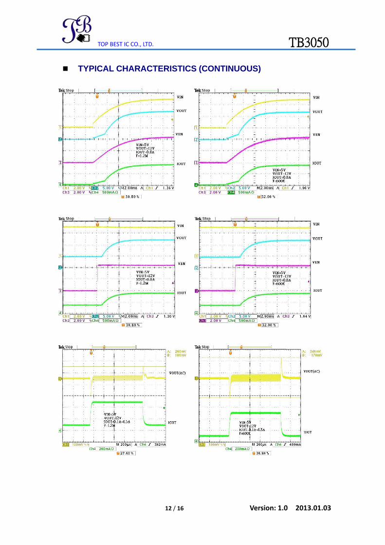
TYPICAL CHARACTERISTICS (CONTINUOUS)
TOP BEST IC CO., LTD. TB3050
12 / 16 Version: 1.0 2013.01.03
TYPICAL CHARACTERISTICS (CONTINUOUS)

TOP BEST IC CO., LTD. TB3050
13 / 16 Version: 1.0 2013.01.03
PACKAGE OUTLINES
(1) MSOP-10L-EP
b e
E1 E
1 5
610
"A"
E2
1 5
610
D1
THERMALLY ENHANCED VARIATIONS ONLY
AA2
A1
D
C
0.05
H
0.25
LL1 θ
GAUGE PLANE
SEATING PLANE
DETAIL A
Symbol Dimensions in Millimeters Dimensions in Inches
Min. Nom. Max. Min. Nom. Max.
A - - 1.1 - - 0.043
A1 0 0.08 0.15 0 0.003 0.006
A2 0.75 0.85 0.95 0.03 0.034 0.038
C 0.08 0.15 0.23 0.003 0.006 0.009
D 2.9 3 3.1 0.114 0.118 0.122
D1 0.75 1.63 2.5 0.03 0.064 0.098
E 4.8 4.9 5 0.189 0.193 0.197
E1 2.9 3 3.1 0.114 0.118 0.122
E2 0.75 1.63 2.5 0.03 0.064 0.098
L 0.4 0.6 0.8 0.016 0.024 0.031
b 0.22 0.3 0.38 0.009 0.012 0.015
e 0.50 BSC 0.020 BSC
y - - 0.1 - - 0.004
0O - 8O 0O - 8O
JEDEC outline: MO-187 BA-T

TOP BEST IC CO., LTD. TB3050
14 / 16 Version: 1.0 2013.01.03
(2) MSOP-8L-EP
DETAIL A
L
EE1
AA2
A1e
D
7 (4X)
b
y
C
DETAIL A
E2
D1
Expose
Pad
1 4
58
Symbol Dimensions in Millimeters Dimensions in Inches
Min. Nom. Max. Min. Nom. Max.
A - - 1.1 - - 0.043
A1 0 0.08 0.15 0 0.003 0.006
A2 0.75 0.85 0.95 0.03 0.034 0.038
C 0.08 0.15 0.23 0.003 0.006 0.009
D 2.9 3 3.1 0.114 0.118 0.122
D1 0.75 1.63 2.5 0.03 0.064 0.098
E 4.8 4.9 5 0.189 0.193 0.197
E1 2.9 3 3.1 0.114 0.118 0.122
E2 0.75 1.63 2.5 0.03 0.064 0.098
L 0.4 0.6 0.8 0.016 0.024 0.031
b 0.22 0.3 0.38 0.009 0.012 0.015
e 0.65 BSC 0.026 BSC
y - - 0.1 - - 0.004
0O - 8O 0O - 8O
JEDEC outline: MO-187 AA-T

TOP BEST IC CO., LTD. TB3050
15 / 16 Version: 1.0 2013.01.03
(3) SOP-8L-EP
DETAIL A
L
HE
AA2
A1e
D
7 (4X)
b
y
C
DETAIL A
Y
X
Expose Pad θ
Symbol Dimensions in Millimeters Dimensions in Inches
Min. Nom. Max. Min. Nom. Max.
A - - 1.75 - - 0.069
A1 0 - 0.15 0 - 0.06
A2 1.25 - - 0.049 - -
C 0.1 0.2 0.25 0.0075 0.008 0.01
D 4.7 4.9 5.1 0.185 0.193 0.2
E 3.7 3.9 4.1 0.146 0.154 0.161
H 5.8 6 6.2 0.228 0.236 0.244
L 0.4 - 1.27 0.015 - 0.05
b 0.31 0.41 0.51 0.012 0.016 0.02
e 1.27 BSC 0.050 BSC
y - - 0.1 - - 0.004
X - 2.34 - - 0.092 -
Y - 2.34 - - 0.092 -
θ 0O - 8O 0O - 8O
Mold flash shall not exceed 0.25mm per side JEDEC outline: MS-012 BA

TOP BEST IC CO., LTD. TB3050
16 / 16 Version: 1.0 2013.01.03
(4) TDFN-10L (3*3 0.75mm)
E
D
A
A1
A3
D2
e
E2
L
(Top View)(Bottom View)
b
Pin1
SEATING PLANE
(SIDE View)
Symbol Dimensions in Millimeters Dimensions in Inches
Min. Nom. Max. Min. Nom. Max.
A 0.70 0.75 0.80 0.028 0.030 0.031
A1 0.00 0.02 0.05 0.000 0.001 0.002
A3 0.20 REF. 0.008 REF.
b 0.18 0.25 0.30 0.007 0.010 0.012
D 2.90 3.00 3.10 0.114 0.118 0.122
D2 2.20 2.40 2.50 0.087 0.094 0.098
E 2.90 3.00 3.10 0.114 0.118 0.122
E2 1.50 1.60 1.70 0.059 0.063 0.070
e 0.50 BSC. 0.020 BSC.
L 0.30 0.40 0.50 0.012 0.016 0.020


![AJOAA05U UH M MH UHC MHC-899 - Wing On Traveltoursimagery.wingontravel.com/Site/Upload/GroupTour/danzhang/... · ` 27v ,NAP 60:ax1+,; x1+,; w~_I_XZ`nn ... SoG|Hf]Dv|55Di5kM](https://static.fdocuments.us/doc/165x107/5ab557987f8b9a1a048cb941/ajoaa05u-uh-m-mh-uhc-mhc-899-wing-on-27v-nap-60ax1-x1-wixznn-soghfdv55di5kmiev.jpg)