GENERAL DESCRIPTION FEATURES - 虹冠電子 Device/CM6805.pdfCM6805(A;B)/CM6806A 10-PIN Green-Mode...
16
CM6805(A;B)/CM6806A 10-PIN Green-Mode PFC/PWM Combo CONTROLLER for High Density AC Adapter 2006/10/11 Rev1.0 Champion Microelectronic Corporation Page 1 GENERAL DESCRIPTION FEATURES The CM6805A and CM6806A are the Green-Mode PFC/PWM Combo controller for High Density AC Adapter. For the power supply, its input current shaping PFC performance could be very close to the performance of the CM6800 or ML4800 leading edge modulation average current topology. Both PFC and PWM have the Green Mode to meet blue angel and energy star spec. 10-Pin SOIC package PWM pulse skipping for the green mode Use RAC as the Startup resistor around 5 Mega Ohm at IAC pin It can use the HV bipolar to start up the chip and it helps green mode. Easy to configure into Boost Follower Enable lowest BOM for power supply with PFC Internally synchronized PFC and PWM in one IC Patented slew rate enhanced voltage error amplifier with advanced input current shaping technique Universal Line Input Voltage CCM boost or DCM boost with leading edge modulation PFC using Input Current Shaping Technique Feedforward IAC pin to do the automatic slope compensation PFCOVP, VCCOVP, Precision -1V PFC ILIMIT, PFC Tri-Fault Detect comparator to meet UL1950 Low supply currents; start-up: 100uA typical, operating current: 2mA typical. Synchronized leading PFC and trailing edge modulation PWM to reduce ripple current in the storage capacitor between the PFC and PWM sections and to reduce switching noise in the system VINOK Comparator to guarantee to enable PWM when PFC reach steady state High efficiency trailing-edge current mode PWM Exact 50% PWM maximum duty cycle UVLO, REFOK, and brownout protection Digital PFC and PWM soft start, ~10mS Precision PWM 1.5V current limit for current mode operation PWMtrifault to sense DC to DC short and Turn off PFC at GMth PWMtrifault also can be programmed to do the Thermal Protection CM6805A/CM6806A offers the use of smaller, lower cost bulk capacitors, reduces power line loading and stress on the switching FETs, and results in a power supply fully compliant to IEC1000-3-2 specifications. The CM6805A / CM6806A includes circuits for the implementation of a leading edge, input current shaping technique “boost” type PFC and a trailing edge, PWM. The CM6805A’s PFC and PWM operate at the same frequency, 67.5kHz. A PFC OVP comparator shuts down the PFC section in the event of a sudden decrease in load. The PFC section also includes peak current limiting for enhanced system reliability. Both PFC and PWM have the Green Mode Functions. When the load is below GMth, Green Mode Threshold, PFCOUT is turned off. The GMth can be programmed by the designer. PWM Green Mode will happen when the PWMCMP (PWM Comparator) Duty Cycle is less than ~ 6%, in the next cycle, the PWMOUT pulse will be removed until PWMCMP Duty Cycle is greater than 6%, then the next cycle, PWMOUT pulse appears. PWM has a PWMtrifault pin which can sense the PWM short and determine the GMth to turn off PFC.
Transcript of GENERAL DESCRIPTION FEATURES - 虹冠電子 Device/CM6805.pdfCM6805(A;B)/CM6806A 10-PIN Green-Mode...
CM6805(A;B)/CM6806A 10-PIN Green-Mode PFC/PWM Combo CONTROLLER for High Density AC Adapter
2006/10/11 Rev1.0 Champion Microelectronic Corporation Page 1
GENERAL DESCRIPTION
FEATURES
The CM6805A and CM6806A are the Green-Mode PFC/PWM Combo controller for High Density AC Adapter. For the power supply, its input current shaping PFC performance could be very close to the performance of the CM6800 or ML4800 leading edge modulation average current topology.
Both PFC and PWM have the Green Mode to meet blue angel and energy star spec.
10-Pin SOIC package PWM pulse skipping for the green mode Use RAC as the Startup resistor around 5 Mega Ohm at
IAC pin It can use the HV bipolar to start up the chip and it helps
green mode. Easy to configure into Boost Follower Enable lowest BOM for power supply with PFC Internally synchronized PFC and PWM in one IC Patented slew rate enhanced voltage error amplifier with
advanced input current shaping technique Universal Line Input Voltage CCM boost or DCM boost with leading edge modulation
PFC using Input Current Shaping Technique Feedforward IAC pin to do the automatic slope
compensation PFCOVP, VCCOVP, Precision -1V PFC ILIMIT, PFC
Tri-Fault Detect comparator to meet UL1950 Low supply currents; start-up: 100uA typical, operating
current: 2mA typical. Synchronized leading PFC and trailing edge modulation
PWM to reduce ripple current in the storage capacitor between the PFC and PWM sections and to reduce switching noise in the system
VINOK Comparator to guarantee to enable PWM when PFC reach steady state
High efficiency trailing-edge current mode PWM Exact 50% PWM maximum duty cycle UVLO, REFOK, and brownout protection Digital PFC and PWM soft start, ~10mS Precision PWM 1.5V current limit for current mode
operation PWMtrifault to sense DC to DC short and Turn off PFC at
GMth PWMtrifault also can be programmed to do the Thermal
Protection
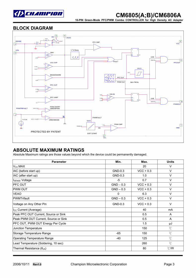
CM6805A/CM6806A offers the use of smaller, lower cost bulk capacitors, reduces power line loading and stress on the switching FETs, and results in a power supply fully compliant to IEC1000-3-2 specifications. The CM6805A / CM6806A includes circuits for the implementation of a leading edge, input current shaping technique “boost” type PFC and a trailing edge, PWM. The CM6805A’s PFC and PWM operate at the same frequency, 67.5kHz. A PFC OVP comparator shuts down the PFC section in the event of a sudden decrease in load. The PFC section also includes peak current limiting for enhanced system reliability. Both PFC and PWM have the Green Mode Functions. When the load is below GMth, Green Mode Threshold, PFCOUT is turned off. The GMth can be programmed by the designer. PWM Green Mode will happen when the PWMCMP (PWM Comparator) Duty Cycle is less than ~ 6%, in the next cycle, the PWMOUT pulse will be removed until PWMCMP Duty Cycle is greater than 6%, then the next cycle, PWMOUT pulse appears. PWM has a PWMtrifault pin which can sense the PWM short and determine the GMth to turn off PFC.

CM6805(A;B)/CM6806A 10-PIN Green-Mode PFC/PWM Combo CONTROLLER for High Density AC Adapter
APPLICATIONS
PIN CONFIGURATION
AC Adaptor
Open Frame
10 Pin SSOP (R10) Top View
7
6
10
9
8
1
2
3
4
GND
IAC
ISENSE
VEAO PWMTRIFAULT
PWM OUT
PFC OUT
VCC
5 VFB V + I
PIN DESCRIPTION Operating Voltage Pin No. Symbol Description Min. Typ. Max. Unit
1 GND Ground
2 IAC Feedforward input to do slope compensation and to start up the system. During the start up, IAC is connected to VCC until VCC is greater than 13V.
0 1 V
3 ISENSE Current sense input to the PFC current limit comparator -5 0.7 V
4 VEAO PFC transconductance voltage error amplifier output 0 6 V
5 VFB PFC transconductance voltage error amplifier input 0 2.5 3 V
6 V + I PWM current limit comparator input 0 1.5 V
7 PWMTRIFAULT PWMTRIFAULT input; it can sense PWM Short or OVP 0 VCC V
8 VCC Positive supply 10 5 18 V
9 PFC OUT PFC driver output 0 VCC V
10 PWM OUT PWM driver output 0 VCC V
ORDERING INFORMATION
Initial Accuracy (KHz) Part Number Operation Frequency
Min Typ Max
Temperature Range Package
CM6805AIR/AGIR* Fpwm = Fpfc = 67.5Khz 60 67 74 -40 to 125 10 Pin SSOP(R10)
CM6805BIR/BGIR* Fpwm = Fpfc = 95Khz 85 95 106 -40 to 125 10 Pin SSOP(R10)
CM6806AIR/AGIR* Fpwm = 2Fpfc = 110Khz 98 110 120 -40 to 125 10 Pin SSOP(R10)
Note: 1.G : Suffix for Pb Free Product 2.Initial Accuracy : TA=25
2006/10/11 Rev1.0 Champion Microelectronic Corporation Page 2
CM6805(A;B)/CM6806A 10-PIN Green-Mode PFC/PWM Combo CONTROLLER for High Density AC Adapter
BLOCK DIAGRAM
VFB
5
UVB
PFCOUT
9
IAC2
GREENMODE
-1V
VCC
2.5V
VREFDK
PWM CLK
-
+
.
.VEAO4
PFC OVP+
-
.-
(VCC-1.4V)/2
PWM CMP
10mS
. .
BROKENWIRE
V=17uA
+
-
.
. .
PROTECTED BY PATENT
+
-
PFCCLK
PWMCLK.
.
PFC ILIMIT
.
.
V To Ramp
VCC OVP+
-
.-
S
R2
Q
Q
R1
R1A.21
fpfc=70KHz
IAC
1.5VGND
R1C.
2
1
VREFDK
PFC CLK
PWMFAULT
+
-
.-
FAULT
UVB
+
-
.
VCC-0.7V
PFC CMP
16.4V
S
R
Q
Q
R
GREENPWM
PWMOUT
10
17.9V
PWMCLK
2.75V
VIN-OK+
-
.-
PWM SHORT
V+I6
VCC
VCC8
GMV
0.5V
2.45V
UVLO
. .
GND
+
-
.
+
-
+
-
UVB
PWMTRIFAULT
7
VFB
R1B.21
GND
1
ISENSE
3
0.75V
SS
2.5V
SOFT START
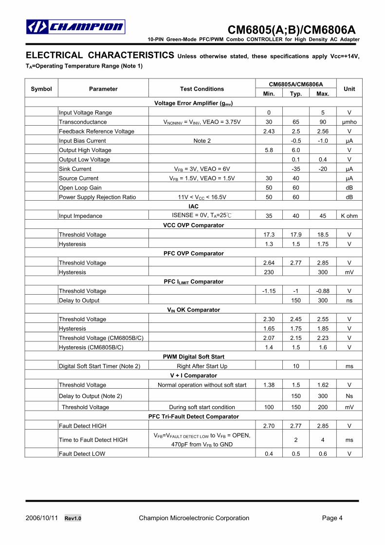
ABSOLUTE MAXIMUM RATINGS Absolute Maximum ratings are those values beyond which the device could be permanently damaged.
Parameter Min. Max. Units VCC MAX 20 V IAC (before start up) GND-0.3 VCC + 0.3 V IAC (after start up) GND-0.3 1.0 V ISENSE Voltage -5 0.7 V PFC OUT GND – 0.3 VCC + 0.3 V PWM OUT GND – 0.3 VCC + 0.3 V VEAO 0 6.3 V PWMTrifault GND – 0.3 VCC + 0.3 V
Voltage on Any Other Pin GND-0.3 VCC + 0.3 V
ICC Current (Average) 40 mA Peak PFC OUT Current, Source or Sink 0.5 A Peak PWM OUT Current, Source or Sink 0.5 A PFC OUT, PWM OUT Energy Per Cycle 1.5 μJ Junction Temperature 150
Storage Temperature Range -65 150
Operating Temperature Range -40 125
Lead Temperature (Soldering, 10 sec) 260
Thermal Resistance (θJA) 80 /W
2006/10/11 Rev1.0 Champion Microelectronic Corporation Page 3
CM6805(A;B)/CM6806A 10-PIN Green-Mode PFC/PWM Combo CONTROLLER for High Density AC Adapter
2006/10/11 Rev1.0 Champion Microelectronic Corporation Page 4
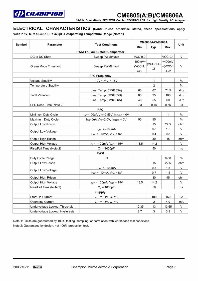
ELECTRICAL CHARACTERISTICS Unless otherwise stated, these specifications apply Vcc=+14V, TA=Operating Temperature Range (Note 1)
CM6805A/CM6806A Symbol Parameter Test Conditions
Min. Typ. Max. Unit
Voltage Error Amplifier (gmv) Input Voltage Range 0 5 V Transconductance VNONINV = VINV, VEAO = 3.75V 30 65 90 μmho Feedback Reference Voltage 2.43 2.5 2.56 V Input Bias Current Note 2 -0.5 -1.0 μA Output High Voltage 5.8 6.0 V Output Low Voltage 0.1 0.4 V Sink Current VFB = 3V, VEAO = 6V -35 -20 μA Source Current VFB = 1.5V, VEAO = 1.5V 30 40 μA Open Loop Gain 50 60 dB Power Supply Rejection Ratio 11V < VCC < 16.5V 50 60 dB
IAC Input Impedance ISENSE = 0V, TA=25 35 40 45 K ohm
VCC OVP Comparator Threshold Voltage 17.3 17.9 18.5 V Hysteresis 1.3 1.5 1.75 V
PFC OVP Comparator Threshold Voltage 2.64 2.77 2.85 V Hysteresis 230 300 mV
PFC ILIMIT Comparator Threshold Voltage -1.15 -1 -0.88 V Delay to Output 150 300 ns
VIN OK Comparator Threshold Voltage 2.30 2.45 2.55 V Hysteresis 1.65 1.75 1.85 V Threshold Voltage (CM6805B/C) 2.07 2.15 2.23 V Hysteresis (CM6805B/C) 1.4 1.5 1.6 V
PWM Digital Soft Start Digital Soft Start Timer (Note 2) Right After Start Up 10 ms
V + I Comparator Threshold Voltage Normal operation without soft start 1.38 1.5 1.62 V
Delay to Output (Note 2) 150 300 Ns
Threshold Voltage During soft start condition 100 150 200 mV PFC Tri-Fault Detect Comparator
Fault Detect HIGH 2.70 2.77 2.85 V
Time to Fault Detect HIGH VFB=VFAULT DETECT LOW to VFB = OPEN,
470pF from VFB to GND 2 4 ms
Fault Detect LOW 0.4 0.5 0.6 V
CM6805(A;B)/CM6806A 10-PIN Green-Mode PFC/PWM Combo CONTROLLER for High Density AC Adapter
2006/10/11 Rev1.0 Champion Microelectronic Corporation Page 5
ELECTRICAL CHARACTERISTICS (Conti.)Unless otherwise stated, these specifications apply Vcc=+15V, RT = 52.3kΩ, CT = 470pF,TA=Operating Temperature Range (Note 1)
CM6805A/CM6806A Symbol Parameter Test Conditions
Min. Typ. Max. Unit
PWM Tri-Fault Detect Comparator DC to DC Short Sweep PWMtrifault VCC-0.9 VCC-0.1 V
Green Mode Threshold Sweep PWMtrifault -400mV+(VCC-1.
4)/2
(VCC-1.4)/2
+400mV+(VCC-1
.4)/2 V
PFC Frequency Voltage Stability 10V < VCC < 15V 1 % Temperature Stability 2 %
Line, Temp (CM6805A) 60 67 74.5 kHz Line, Temp (CM6805B) 85 95 106 kHz Total Variation Line, Temp (CM6806A) 49 55 60 kHz
PFC Dead Time (Note 2) 0.3 0.45 0.65 us PFC
Minimum Duty Cycle IAC=100uA,VFB=2.55V, ISENSE = 0V 1 % Maximum Duty Cycle IAC=0uA,VFB=2.0V, ISENSE = 0V 90 95 % Output Low Rdson 15 22.5 ohm
IOUT = -100mA 0.8 1.5 V Output Low Voltage
IOUT = -10mA, VCC = 8V 0.4 0.8 V Output High Rdson 30 45 ohm Output High Voltage IOUT = 100mA, VCC = 15V 13.5 14.2 V Rise/Fall Time (Note 2) CL = 1000pF 50 ns
PWM Duty Cycle Range IC 0-50 % Output Low Rdson 15 22.5 ohm
IOUT = -100mA 0.8 1.5 V Output Low Voltage
IOUT = -10mA, VCC = 8V 0.7 1.5 V Output High Rdson 30 45 ohm Output High Voltage IOUT = 100mA, VCC = 15V 13.5 14.2 V Rise/Fall Time (Note 2) CL = 1000pF 50 ns
Supply Start-Up Current VCC = 11V, CL = 0 100 150 uA Operating Current VCC = 15V, CL = 0 2 4.0 mA Undervoltage Lockout Threshold 12.35 13 13.65 V Undervoltage Lockout Hysteresis 2.7 3 3.3 V
Note 1: Limits are guaranteed by 100% testing, sampling, or correlation with worst-case test conditions. Note 2: Guaranteed by design, not 100% production test.
CM6805(A;B)/CM6806A 10-PIN Green-Mode PFC/PWM Combo CONTROLLER for High Density AC Adapter
TYPICAL PERFORMANCE CHARACTERISTIC
57
64
71
78
85
92
99
106
113
120
127
2 2.1 2.2 2.3 2.4 2.5 2.6 2.7 2.8 2.9 3
VFB (V)
Tran
scon
duct
ance
(um
ho)
Voltage Error Amplifier (gmv) Transconductance
2006/10/11 Rev1.0 Champion Microelectronic Corporation Page 6
CM6805(A;B)/CM6806A 10-PIN Green-Mode PFC/PWM Combo CONTROLLER for High Density AC Adapter
2006/10/11 Rev1.0 Champion Microelectronic Corporation Page 7
Functional Description The CM6805A/CM6806A consists of an ICST (Input Current Shaping Technique), CCM (Continuous Conduction Mode) or DCM (Discontinuous Conduction Mode) boost PFC (Power Factor Correction) front end and a synchronized PWM (Pulse Width Modulator) back end. The CM6805A /CM6806A is designed to replace FAN6803 (8pin SOP package), which is the second generation of the ML4803 with 8 pin package. It is distinguished from earlier combo controllers by its low count, innovative input current shaping technique, and very low start-up and operating currents. The PWM section is dedicated to peak current mode operation. It uses conventional trailing-edge modulation, while the PFC uses leading-edge modulation. This patented Leading Edge/Trailing Edge (LETE) modulation technique helps to minimize ripple current in the PFC DC buss capacitor.
The main improvements from ML4803 are: 1. Add Green Mode Functions for both PFC and PWM 2. Remove the one pin error amplifier and add back the
slew rate enhancement gmv, which is using voltage input instead of current input. This transconductance amplifier will increase the transient response 5 to 10 times from the conventional OP
3. VFB PFC OVP comparator 4. PFC Tri-Fault Detect for UL1950 compliance and
enhanced safety 5. A feedforward signal from IAC pin is added to do the
automatic slope compensation. This increases the signal to noise ratio during the light load; therefore, THD is improved at light load and high input line voltage.
6. CM6805A/CM6806A does not require the bleed resistor and it uses the more than 800k ohm resistor between IAC pin and rectified line voltage to feed the initial current before the chip wakes up.
7. VINOK comparator is added to guaranteed PWM cannot turn on until VFB reaches 2.5V in which PFC boost output is about steady state, typical 380V.
8. A 10mS digital PWM soft start circuit is added 9. 10 pin SOP package 10. No internal Zener but with VCCOVP comparator The CM6805A/CM6806A operates both PFC and PWM sections at 67kHz. This allows the use of smaller PWM magnetic and output filter components, while minimizingswitching losses in the PFC stage. Several protection features have been built into the CM6805A/CM6806A. These include soft-start, redundant PFC overvoltage protection, PFC Tri-Fault Detect, VINOK, peak current limiting, duty cycle limiting, under-voltage lockout, reference ok comparator and VCCOVP.
Detailed Pin Descriptions IAC (Pin 2) Typically, it has a feedforward resistor, RAC, 800K~5KK ohm resistor connected between this pin and rectified line input voltage. This pin serves 2 purposes:
1.) During the startup condition, it supplies the startup current; therefore, the system does not requires additional bleed resistor to start up the chip.
2.) The current of RAC will program the automatic slope compensation for the system. This feedforward signal can increase the signal to noise ratio for the light load condition or the high input line voltage condition.
ISENSE (Pin 3) This pin ties to a resistor which senses the PFC input current. This signal should be negative with respect to the IC ground. It internally feeds the pulse-by-pulse current limit comparator and the current sense feedback signal. The ILIMIT trip level is –1V. The ISENSE feedback is internally multiplied by a gain of four and compared against the internal programmed ramp to set the PFC duty cycle. The intersection of the boost inductor current downslope with theinternal programming ramp determines the boost off-time. It requires a RC filter between ISENSE and PFC boost sensing resistor. VEAO (Pin 4) This is the PFC slew rate enhanced transconductance amplifier output which needs to connected with a compensation network Ground. VFB (Pin 5) Besides this is the PFC slew rate enhanced transconductance input, it also tie to a couple of protectioncomparators, PFCOVP, and PFC Tri-Fault Detect V + I (Pin 6) This pin is tied to the primary side PWM current sense resistor or transformer. It provides the internal pulse-by-pulse current limit for the PWM stage (which occurs at 1.5V) and the peak current mode feedback path for the current mode control of the PWM stage. Besides current information, the optocouple also goes into V + I pin. Therefore, it is the SUM Amplifier input. Soft Start can be triggered by the following conditions: 1.) During the startup (VCC is less than 10V) 2.) DC to DC short (PWMtrifault is greater thanVCC-0.7V)
CM6805(A;B)/CM6806A 10-PIN Green-Mode PFC/PWM Combo CONTROLLER for High Density AC Adapter
PWMtrifault (Pin 7) This pin is to monitor the DC to DC faults. PWMtrifault monitors the voltage which is translated by the photocouple output current. When the output is short, photocouple and TL431 will not draw any current and PWMtrifault will go toward VCC. When PWMtrifault is above VCC-0.7V, the soft start will be triggered and PWMOUT is turned off. When the load is lighter, the TL431 will increase the Photocouple current. When PWMtrifault is below (VCC-1.4)/2, which means it is below GMth, Green Mode Threshold. PFCOUT will be turned off due the load is below GMth. The GMth can be programmed by the user. Typical the GMth is 20% of the full load. VCC (Pin 8) VCC is the power input connection to the IC. The VCC start-up current is 100uA. The no-load ICC current is 2mA. VCC quiescent current will include both the IC biasing currents and the PFC and PWM output currents. Given the operating frequency and the MOSFET gate charge (Qg), average PFC and PWM output currents can be calculated as IOUT = Qg x F. The average magnetizing current required for any gate drive transformers must also be included. The VCC pin is also assumed to be proportional to the PFC output voltage. Internally it is tied to the VCC OVP comparator (17.9V) providing redundant high-speed over-voltage protection (OVP) of the PFC stage. VCC also ties internally to the UVLO circuitry and VREFOK comparator, enabling the IC at 13V and disabling it at 10V. VCC must be bypassed with a high quality ceramic bypass capacitor placed as close as possible to the IC. Good bypassing is critical to the proper operation of the CM6805A/CM6806A. VCC is typically produced by an additional winding off the boost inductor or PFC Choke, providing a voltage that is proportional to the PFC output voltage. Since the VCC OVP max voltage is 17.9V, an internal shunt limits VCC overvoltage to an acceptable value. An external clamp, such as shown in Figure 1, is desirable but not necessary.
VCC
GND
1N5250B
Figure 1. Optional VCC Clamp This limits the maximum VCC that can be applied to the IC while allowing a VCC which is high enough to trip the VCC OVP. An RC filter at VCC is required between boost trap winding and VCC.
PFCOUT (Pin 9) and PWM OUT (Pin 10) PFC OUT and PWM OUT are the high-current power driver capable of directly driving the gate of a power MOSFET with peak currents up to -1A and +0.5A. Both outputs are actively held low when VCC is below the UVLO threshold level which is 15V or VREFOK comparator is low. Power Factor Correction Power factor correction makes a nonlinear load look like a resistive load to the AC line. For a resistor, the current drawn from the line is in phase with and proportional to the line voltage, so the power factor is unity (one). A common class of nonlinear load is the input of most power supplies, which use a bridge rectifier and capacitive input filter fed from the line. The peak-charging effect, which occurs on the input filter capacitor in these supplies, causes brief high-amplitude pulses of current to flow from the power line, rather than a sinusoidal current in phase with the line voltage. Such supplies present a power factor to the line of less than one (i.e. they cause significant current harmonics of the power line frequency to appear at their input). If the input current drawn by such a supply (or any other nonlinear load) can be made to follow the input voltage in instantaneous amplitude, it will appear resistive to the AC line and a unity power factor will be achieved. To hold the input current draw of a device drawing power from the AC line in phase with and proportional to the input voltage, a way must be found to prevent that device from loading the line except in proportion to the instantaneous line voltage. The PFC section of the CM6805A/CM6806A uses a boost-mode DC-DC converter to accomplish this. The input to the converter is the full wave rectified AC line voltage. No bulk filtering is applied following the bridge rectifier, so the input voltage to the boost converter ranges (at twice line frequency) from zero volts to the peak value of the AC input and back to zero. By forcing the boost converter to meet two simultaneous conditions, it is possible to ensure that the current draws from the power line matches the instantaneous line voltage. One of these conditions is that the output voltage of the boost converter must be set higher than the peak value of the line voltage. A commonly used value is 385VFB, to allow for a high line of 270VACrms. The other condition is that the current that the converter is allowed to draw from the line at any given instant must be proportional to the line voltage.
2006/10/11 Rev1.0 Champion Microelectronic Corporation Page 8
CM6805(A;B)/CM6806A 10-PIN Green-Mode PFC/PWM Combo CONTROLLER for High Density AC Adapter
PFC Control: Leading Edge Modulation with Input Current Shaping Technique (I.C.S.T.) The only differences between the conventional PFC control topology and I.C.S.T. is: the current loop of the conventional control method is a close loop method and it requires a detail understanding about the system loop gain to design. With I.C.S.T., since the current loop is an open loop, it is very straightforward to implement it. The end result of the any PFC system, the power supply is like a pure resistor at low frequency. Therefore, current is in phase with voltage. In the conventional control, it forces the input current tofollow the input voltage. In CM6805A/CM6806A, the chip thinks if a boost converter needs to behave like a low frequency resistor, what the duty cycle should be. The following equations is CM6805A/CM6806A try to achieve:
in
ine I
VR = (1)
inl II = (2)
Equation 2 means: average boost inductor current equals to input current.
doutlin IVIV ×≈×∴ (3)
Therefore, input instantaneous power is about to equal to the output instantaneous power. For steady state and for the each phase angle, boost converter DC equation at continuous conduction mode is:
)1(1
dVV
in
out−= (4)
Rearrange above equations, (1), (2),(3), and (4) in term of Vout and d, boost converter duty cycle and we can getaverage boost diode current equation (5):
e
outd R
VdI ×−=2)1( (5)
Also, the average diode current can be expressed as:
dttIT
I offT
dsw
d ⋅= ∫ )(10
(6)
If the value of the boost inductor is large enough, we can assume . It means during each cycle or we
can say during the sampling, the diode current is a constant.
dd ItI ~)(
Therefore, equation (6) becomes:
)1(' dIdITtII dd
sw
offdd −×=×=
×= (7)
Combine equation (7) and equation (5), and we get:
sw
off
e
outd
e
outd
e
outd
Tt
RVI
RVdI
RVddI
×=∴
×=∴
×=×
'
2'' )(
(8)
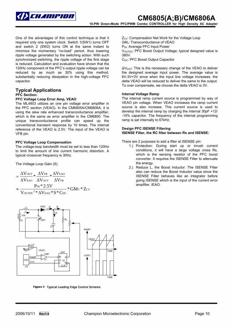
From this simple equation (8), we implement the PFC control section of the CM6805A/CM6806A. Leading/Trailing Modulation Conventional Pulse Width Modulation (PWM) techniques employ trailing edge modulation in which the switch will turn ON right after the trailing edge of the system clock. The error amplifier output is then compared with the modulating ramp. When the modulating ramp reaches the level of the error amplifier output voltage, the switch will be turned OFF. When the switch is ON, the inductor current will ramp up. The effective duty cycle of the trailing edge modulation is determined during the ON time of the switch. Figure 2 shows a typical trailing edge control scheme. In case of leading edge modulation, the switch is turned OFF right at the leading edge of the system clock. When the modulating ramp reaches the level of the error amplifier output voltage, the switch will be turned ON. The effective duty-cycle of the leading edge modulation is determined during OFF time of the switch. Figure 3 shows a leading edge control scheme.
2006/10/11 Rev1.0 Champion Microelectronic Corporation Page 9
CM6805(A;B)/CM6806A 10-PIN Green-Mode PFC/PWM Combo CONTROLLER for High Density AC Adapter
One of the advantages of this control technique is that it required only one system clock. Switch 1(SW1) turns OFF and switch 2 (SW2) turns ON at the same instant to minimize the momentary “no-load” period, thus lowering ripple voltage generated by the switching action. With such synchronized switching, the ripple voltage of the first stage is reduced. Calculation and evaluation have shown that the 120Hz component of the PFC’s output ripple voltage can be reduced by as much as 30% using this method, substantially reducing dissipation in the high-voltage PFC capacitor. Typical Applications PFC Section: PFC Voltage Loop Error Amp, VEAO The ML4803 utilizes an one pin voltage error amplifier in the PFC section (VEAO). In the CM6805A/CM6806A, it is using the slew rate enhanced transconductance amplifier, which is the same as error amplifier in the CM6800. The unique transconductance profile can speed up the conventional transient response by 10 times. The internal reference of the VEAO is 2.5V. The input of the VEAO is VFB pin. PFC Voltage Loop Compensation The voltage-loop bandwidth must be set to less than 120Hz to limit the amount of line current harmonic distortion. A typical crossover frequency is 30Hz. The Voltage Loop Gain (S)
CVVDCEAO
2OUTDC
IN
FB
EAO
OUT
FB
EAO
OUT
Z*GM*C*S*V*V
V5.2*PV
V*VV*
VV
Δ≈
ΔΔ
ΔΔ
ΔΔ
=
ZCV: Compensation Net Work for the Voltage Loop GMv: Transconductance of VEAO PIN: Average PFC Input Power VOUTDC: PFC Boost Output Voltage; typical designed value is 380V. CDC: PFC Boost Output Capacitor ΔVEAO: This is the necessary change of the VEAO to deliver the designed average input power. The average value is6V-3V=3V since when the input line voltage increases, the delta VEAO will be reduced to deliver the same to the output. To over compensate, we choose the delta VEAO is 3V. Internal Voltage Ramp The internal ramp current source is programmed by way of VEAO pin voltage. When VEAO increases the ramp current source is also increase. This current source is used to develop the internal ramp by charging the internal 30pF +12/ -10% capacitor. The frequency of the internal programming ramp is set internally to 67kHz. Design PFC ISENSE Filtering ISENSE Filter, the RC filter between Rs and ISENSE: There are 2 purposes to add a filter at ISENSE pin:
1.) Protection: During start up or inrush current conditions, it will have a large voltage cross Rs,which is the sensing resistor of the PFC boost converter. It requires the ISENSE Filter to attenuate the energy.
2.) Reduce L, the Boost Inductor: The ISENSE Filter also can reduce the Boost Inductor value since the ISENSE Filter behaves like an integrator before going ISENSE which is the input of the current error amplifier, IEAO.
2006/10/11 Rev1.0 Champion Microelectronic Corporation Page 10

CM6805(A;B)/CM6806A 10-PIN Green-Mode PFC/PWM Combo CONTROLLER for High Density AC Adapter
2006/10/11 Rev1.0 Champion Microelectronic Corporation Page 11
The ISENSE Filter is a RC filter. The resistor value of the ISENSE Filter is between 100 ohm and 50 ohm. By selecting RFILTER equal to 50 ohm will keep the offset of the IEAO less than 5mV. Usually, we design the pole of ISENSE Filter at fpfc/6, one sixth of the PFC switching frequency. Therefore, the boost inductor can be reduced 6 times without disturbing the stability. Therefore, the capacitor of the ISENSE
Filter, CFILTER, will be around 283nF. IAC, RAC, Automatic Slope Compensation, DCM at high line and light load, and Startup current There are 4 purposes for IAC pin:
1.) For the leading edge modulation, when the duty cycle is less than 50%, it requires the similar slope compensation, as the duty cycle of the trailing edge modulation is greater than 50%. In the CM6805A/CM6806A, it is a relatively easy thing to design. Use an more than 800K ohm resistor, RAC
to connect IAC pin and the rectified line voltage. It will do the automatic slope compensation. If the input boost inductor is too small, the RAC may need to be reduced more.
2.) During the startup period, Rac also provides the initial startup current, 100uA;therefore, the bleed resistor is not needed.
3.) Since IAC pin with RAC behaves as a feedforward signal, it also enhances the signal to noise ratioand the THD of the input current.
4.) It also will try to keep the maximum input power to be constant. However, the maximum input power will still go up when the input line voltage goes up.
Start Up of the system, UVLO, VREFOK and Soft Start During the Start-up period, RAC resistor will provide the start up current~100uA from the rectified line voltage to IAC pin. Inside of CM6805A/CM6806A during the start-up period, IAC is connected to VCC until the VCC reaches UVLO voltage which is 15V and internal reference voltage is stable, it will disconnect itself from VCC. During the Start up, the soft start function is triggered and the duration of the soft start will last around 10mS. PFC section wakes up after Start up period After Start up period, PFC section will softly start since VEAO is zero before the start-up period. Since VEAO is a slew rate enhanced transconductance amplifier (see figure3), VEAO has a high impedance output like a current source and it will slowly charge the compensation net work which needs to be designed by using the voltage loop gain equation. Before PFC boost output reaches its design voltage, it isaround 380V and VFB reaches 2.5V, PWM section is off.
PWM section wakes up after PFC reaches steady state PWM section is off all the time before PFC VFB reaches 2.45V. Then internal 10mS digital PWM soft start circuit slowly ramps up the soft-start voltage. PFC OVP Comparator PFC OVP Comparator sense VFB pin which is the same the voltage loop input. The good thing is the compensationnetwork is connected to VEAO. The PFC OVP function is a relative fast OVP. It is not like the conventional error amplifier which is an operational amplifier and it requires a local feedback and it make the OVP action becomes very slow. The threshold of the PFC OVP is 2.5V+10% =2.75V with 250mV hysteresis. PFC Tri-Fault Detect Comparator To improve power supply reliability, reduce system component count, and simplify compliance to UL1950 safety standards, the CM6805A/CM6806A includes PFC Tri-Fault Detect. This feature monitors VFB (Pin 5) for certain PFC fault conditions. In case of a feedback path failure, the output of the PFC could go out of safe operating limits. With such a failure, VFB will go outside of its normal operating area. Should VFB go too low, too high, or open, PFC Tri-Fault Detect senses the error and terminates the PFC output drive. PFC Tri-Fault detect is an entirely internal circuit. It requires no external components to serve its protective function. VCC OVP and generate VCC For the CM6805A/CM6806A system, if VCC is generated from a source that is proportional to the PFC output voltageand once that source reaches 17.9V, PFCOUT, PFC driver will be off. The VCC OVP resets once the VCC discharges below16.4V, PFC output driver is enabled. It serves as redundant PFC OVP function. Typically, there is a bootstrap winding off the boost inductor. The VCC OVP comparator senses when this voltage exceeds 17.9V, and terminates the PFC output drive. Once the VCC rail has decreased to below 16.4V the PFC output drive be enabled. Given that 16V on VCC corresponds to 380V on the PFC output, 17.9V on VCC corresponds to an OVP level of 460V. It is a necessary to put RC filter between bootstrap winding and VCC. For VCC=15V, it is sufficient to drive either a power MOSFET or a IGBT.
CM6805(A;B)/CM6806A 10-PIN Green-Mode PFC/PWM Combo CONTROLLER for High Density AC Adapter
2006/10/11 Rev1.0 Champion Microelectronic Corporation Page 12
UVLO The UVLO threshold is 13V providing 3V hysteresis. PFCOUT and PWMOUT Both PFCOUT and PWMOUT are CMOS drivers. They both have adaptive anti-shoot through to reduce the switching loss. Its pull-up is a 30ohm PMOS driver and its pull-downis a 15ohm NMOS driver. It can source 0.5A and sink 1A if the VCC is above 15V. PWM Section Green Mode CM6805A/CM6806A has the green mode function to improve the light load efficiency. PWM Green Mode will happen when the PWMCMP (PWM Comparator) Duty Cycle is less than ~ 6%, in the next cycle, the PWMOUT pulse will be removed until PWMCMP Duty Cycle is greater than 6%, then the next cycle, PWMOUT pulse appears. In other words, during the green mode, PWM switching frequency will reduce to improve the efficiency. With the proper external components, CM6805A/CM6806A can easily meet energy star and blue angel specification. After 10mS digital soft start, CM6805A/CM6806A’s PWM is operating as a typical current mode. It requires a secondary feedback, typically, it is configured with CM431, and photo couple. Since PWM Section is different from CM6800 family, it needs the emitter of the photo couple to connected with V + I instead of the collector. The PWM current information also goes into V + I. Usually, the PWM current informationrequires a RC filter before goes into the V + I. Therefore, V + I actually is a summing node from voltage information which is from photo couple and CM431 and current information which is from one end of PWM sensing resistor and the signal goes through a single pole, RC filterthen enter the V + I pin. This RC filter at DCILMIT also serves several functions:
1.) It protects IC. 2.) It provides level shift for voltage information. 3.) It filters the switching noise from current
information.
At normal operation, the threshold voltage of the V + I pin is 1.5V. When the V + I is greater than 1.5V, PWM output driver will turn off the PWM Power MOSfet. When the Soft Start is triggered, the V+I threshold is around 150mV. Soft Start Can be triggered by the following conditions: 1.) During the startup (VCC is less than 10V) 2.) DC to DC short (PWMtrifault is greater than VCC-0.7V)During above 3 conditions, the V + I threshold is around 150mV until the conditions have been removed. After above 3 conditions have been removed, the internal Soft Start D to A will ramp up the voltage from ~150mV to 2V. Each Soft Start Ramp can last around 10mS. Short (PWMtrifault) When PWMtrifault is greater VCC-0.7V, PWMOUT will be turned off. It can be used to detected the following 2 things: 1.) Short Protection 2.) Thermal Shut Down To achieve above item, it requires a negative temperature coefficient Resistor. The following figure shows the typical circuit for PWMtrifault and V + I pins. Turn off PFC(PWMtrifault) When PWMtrifault is less than (VCC-1.4V)/2, CM6805A/CM6806A will turn off PFC. Usually; it means load has been reduced to a level, which is the level of the Green Mode threshold. Usually, we set the Green Mode threshold around 20% of the full load. After turning off PFC, the efficiency will be increased due to the input voltage is higher and less switching events. Component Reduction Components associated with the VRMS and IEAO pins of a typical PFC controller such as the CM6800 have been eliminated. The PFC power limit and bandwidth does vary with line voltage.

CM6805(A;B)/CM6806A 10-PIN Green-Mode PFC/PWM Combo CONTROLLER for High Density AC Adapter
2006/10/11 Rev1.0 Champion Microelectronic Corporation Page 13
CM6805(A;B)/CM6806A 10-PIN Green-Mode PFC/PWM Combo CONTROLLER for High Density AC Adapter
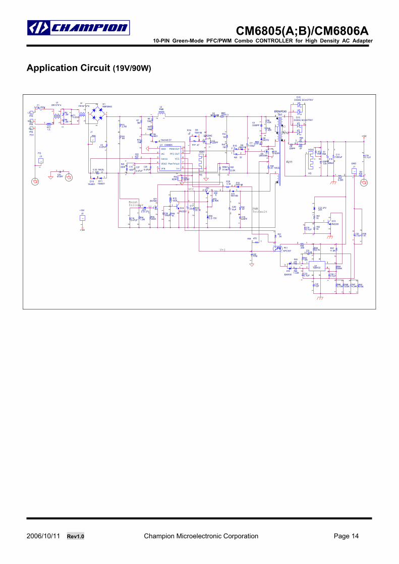
Application Circuit (19V/90W)
3.5*9*1.3D15
DIODE SCHOTTKY
1 2
3
R008-131.6K
12
R474.24K
12
L5RM8
2 1
J1
PIN
1
R2047
1 2
HSA2
HS
11
R112.7M
12
R21 33
1 2
D14
BAW56
23
1
R44205K
12
C15470PF
1 2
R32M
12
C50.47UF
12
L2FR16*12*8
41
32
R190 12
+19V
R5150K
12
PWMTrifault
R843K
12
V+I
D16DIODE SCHOTTKY
1 2
3
Q92SK3569
32
1
FG1PIN
1FG
Q132N2222
3
1
2
Q142N2222
3
1
2
C310.1UF
12
R373K
12
R5847
12
R35205K
12
R5647 12
RT11.5
1 2R62M
12
C22100p
12
Q1015V2 3
1
R281M
12
R181M
12
R462.15K
12
D71N41481 2
C18220PF
12
+19VJ2
11
Q54401
1
23
R341.2M
12
C1722uF
1
2
R312.49K
12
R511K
12
R4843K
12
D82A07G
12 +19V
C160.1UF
12
C251UF
12
C32104pF
12
R5747
12
C8100PF
12
R2522.6K
12
R23330K
12
N1PIN
1N
B002
ZD5Z.D 15V
13
TA1ER39/PC40
3
4 7
5
2
1
9
R160
12 FLY2
U2TSM103
1
2
46
7
3
8
5
R541K
12
VCC
HSA1
HS
1
2
1
2
C230.1UF
12
R50515K
12
D111N4001
12
R451.33K
12
C7100uF
1
2
Q112N7002
23
1
FLY1
D2MUR4601 2
C13105P
12
R17 47
1 2
R260.33 1W(S)1 2
C33300PF
12
C10
680uF
1
2
R431K 12
Q7
2SK2842
32
1
ZD4Z.D 27V
13
R4210K
12
U1 CM6805
2
1
3
4
5 6
7
8
9
10
IAC
GND
Isense
VEAO
VFB V+I
PwmTrif ault
VCC
PFC OUT
PWM OUT
C30220PF
12
R300
1 2
R38 47012
C9220PF
1 2
C33220PF
12
R4111.5K
12
D131N4148
12
C27
0.47UF
12
D61N4148
12
C2810uF
1
2
R3330.1K
12
L1PIN
1L
C190.47UF
12
R3651
12
R55820K
12
R39200
121
2
4
3
PC1KPC357
C240.1UF
12
R240.47 1W(S)
12
F13.15A,250V1 2
C4220PF
12
RT2100K
12
R521K
12
R224701 2
Boostfollower
C200.1UF
12
D101N4001
12
R49255K
12
D121N414812
D91N414812
C10.22UF
12
R4028.7K
12
3.5*6*1.2
FGJ3
11
ZD6Z.D 27V
13
- +
D1KBP206G
2
1
3
4
R3222
12
C210.1UF1 2
C111000uF
1
2
R53150K
12 R14
1M
12
R151M
12
B001
R1375K
12
R270.005
1 2
C260.47UF
12 GND
J1
11
L3OR12*6*4
41
32
R293.3K
1 2
R73M
12
2006/10/11 Rev1.0 Champion Microelectronic Corporation Page 14
CM6805(A;B)/CM6806A 10-PIN Green-Mode PFC/PWM Combo CONTROLLER for High Density AC Adapter
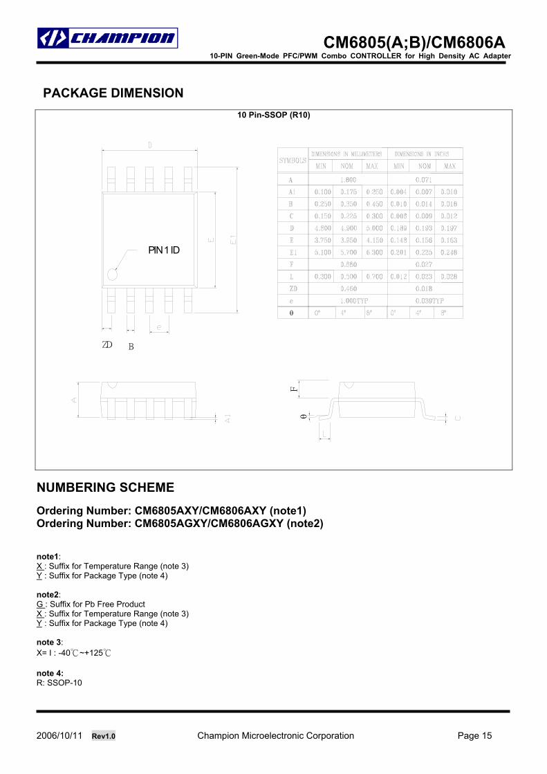
PACKAGE DIMENSION
10 Pin-SSOP (R10)
PIN 1 IDθ
ZD B
F
θ
NUMBERING SCHEME Ordering Number: CM6805AXY/CM6806AXY (note1) Ordering Number: CM6805AGXY/CM6806AGXY (note2) note1: X : Suffix for Temperature Range (note 3) Y : Suffix for Package Type (note 4) note2: G : Suffix for Pb Free Product X : Suffix for Temperature Range (note 3) Y : Suffix for Package Type (note 4) note 3: X= I : -40~+125 note 4: R: SSOP-10
2006/10/11 Rev1.0 Champion Microelectronic Corporation Page 15
CM6805(A;B)/CM6806A 10-PIN Green-Mode PFC/PWM Combo CONTROLLER for High Density AC Adapter
2006/10/11 Rev1.0 Champion Microelectronic Corporation Page 16
IMPORTANT NOTICE Champion Microelectronic Corporation (CMC) reserves the right to make changes to its products or to discontinue any integrated
circuit product or service without notice, and advises its customers to obtain the latest version of relevant information to verify,
before placing orders, that the information being relied on is current.
A few applications using integrated circuit products may involve potential risks of death, personal injury, or severe property or
environmental damage. CMC integrated circuit products are not designed, intended, authorized, or warranted to be suitable for
use in life-support applications, devices or systems or other critical applications. Use of CMC products in such applications is
understood to be fully at the risk of the customer. In order to minimize risks associated with the customer’s applications, the
customer should provide adequate design and operating safeguards.
HsinChu Headquarter Sales & Marketing
5F, No. 11, Park Avenue II, Science-Based Industrial Park, HsinChu City, Taiwan
7F-6, No.32, Sec. 1, Chenggong Rd., Nangang District, Taipei City 115, Taiwan R.O.C.
T E L : +886-3-567 9979 T E L : +886-2-2788 0558 F A X : +886-3-567 9909 F A X : +886-2-2788 2985 http://www.champion-micro.com