Gallium nanoparticles colloids synt hesis for UV bio ...
7
Gallium nanoparticles colloids synthesis for UV bio-optical sensors Flavio Nucciarelli a , Iria Bravo b , Luis Vázquez c , Encarnación Lorenzo b , Jose Luis Pau a a Grupo de Electrónica y Semiconductores, Departamento de Física Aplicada, Universidad Autónoma de Madrid, E-28049 Madrid, Spain b Departamento de Química Analítica y Análisis Instrumental, Universidad Autónoma de Madrid, E- 28049 Madrid, Spain c Instituto de Ciencia de Materiales de Madrid, CSIC, E-28049 Madrid, Spain ABSTRACT A new method for the synthesis of colloidal gallium nanoparticles (Ga NPs) based on the thermal evaporation of Ga on an expendable aluminum zinc oxide (AZO) layer is presented here. The growth of AZO layers was investigated on different substrates at room temperature and 300 ºC. By means of physical evaporation process, nanoparticles were deposited with a distribution ranging from 10 nm to 80 nm in diameter. A study of their endurance in acidic environment was carried out in order to assure the NPs shape and size stability during the etching process. Smaller particles start to disappear between 1h and 2h immersion time in a pH=1 solution, while bigger particles reduce their dimension. The NPs were dispersed in tetrahydrofuran (THF) organic solvent and optically characterized, showing strong UV absorption with a band centered at 280 nm. The colloids size distribution of as-evaporated samples was compared with the distribution obtained in droplets of the solution after drop-casting. By Dipole Discrete Approximation simulations, a close relationship between the UV absorption and the NPs with diameter smaller than ~40 nm was found. Because of the gallium oxide (Ga 1-x O x ) outer shell that surrounds the Ga NPs, an enhancement of their hydrophobicity occurs. Hence, the low agglomeration state between NPs in tetrahydrofuran allows to obtain narrow absorption band in the optical spectrum. Keywords: gallium; nanoparticle; tetrahydrofuran; colloid; bio-sensor; evaporation; zin oxide; 1. INTRODUCTION The use of nanoparticles made of metals or oxide materials has been employed in many of applications such as drug delivery 1 , disinfection 2 and biosensing 3,4 . The key of their success lies on the unique chemical and physical properties of the NPs due to the large surface-to-volume ratio in comparison to the same bulk material. Typically, colloidal NPs are synthetized by chemical process, where the metal salt reacts with further additive in aqueous or organic media. The addition of surfactants for the stability of the colloidal solution is needed, in order to avoid agglomeration. Other fabrication based on physical process are also possible 5,6,7 but the use of toxic reagent makes them less eligible for health-care applications 8 . Recently, the use of gallium nanoparticles has had a main role on cutting edge investigation due to their unique plasmonic characteristic in the UV part of the spectrum 9,10 . Here we propose a new method for the colloidal Ga NPs synthesis. The process involves the physical vapor deposition (PVD) of nanoparticles under vacuum condition on an aluminum zinc oxide expendable layer. The Ga NPs distribution can be modified by changing deposition parameters such as the gallium weight or the evaporation time and power. The use of PVD process reduces the cost, improves the reproducibility of the NP preparation, and enables pre- functionalization and size tuning separately from the selected solvent. The method can be easily scaled to large coverage areas to increase the Ga NP concentration in the colloidal solution. Moreover, in comparison to other methods, it produces a minimum amount of contaminant wastes. Optical Sensors 2017, edited by Francesco Baldini, Jiri Homola, Robert A. Lieberman, Proc. of SPIE Vol. 10231, 1023127 · © 2017 SPIE · CCC code: 0277-786X/17/$18 doi: 10.1117/12.2265883 Proc. of SPIE Vol. 10231 1023127-1
Transcript of Gallium nanoparticles colloids synt hesis for UV bio ...
Gallium nanoparticles colloids synthesis for UV bio-optical sensors
Flavio Nucciarellia, Iria Bravob, Luis Vázquezc, Encarnación Lorenzob, Jose Luis Paua
aGrupo de Electrónica y Semiconductores, Departamento de Física Aplicada, Universidad Autónoma de Madrid, E-28049 Madrid, Spain
bDepartamento de Química Analítica y Análisis Instrumental, Universidad Autónoma de Madrid, E-28049 Madrid, Spain
cInstituto de Ciencia de Materiales de Madrid, CSIC, E-28049 Madrid, Spain
ABSTRACT
A new method for the synthesis of colloidal gallium nanoparticles (Ga NPs) based on the thermal evaporation of Ga on an expendable aluminum zinc oxide (AZO) layer is presented here. The growth of AZO layers was investigated on different substrates at room temperature and 300 ºC. By means of physical evaporation process, nanoparticles were deposited with a distribution ranging from 10 nm to 80 nm in diameter. A study of their endurance in acidic environment was carried out in order to assure the NPs shape and size stability during the etching process. Smaller particles start to disappear between 1h and 2h immersion time in a pH=1 solution, while bigger particles reduce their dimension. The NPs were dispersed in tetrahydrofuran (THF) organic solvent and optically characterized, showing strong UV absorption with a band centered at 280 nm. The colloids size distribution of as-evaporated samples was compared with the distribution obtained in droplets of the solution after drop-casting. By Dipole Discrete Approximation simulations, a close relationship between the UV absorption and the NPs with diameter smaller than ~40 nm was found. Because of the gallium oxide (Ga1-xOx) outer shell that surrounds the Ga NPs, an enhancement of their hydrophobicity occurs. Hence, the low agglomeration state between NPs in tetrahydrofuran allows to obtain narrow absorption band in the optical spectrum.
Keywords: gallium; nanoparticle; tetrahydrofuran; colloid; bio-sensor; evaporation; zin oxide;
1. INTRODUCTION The use of nanoparticles made of metals or oxide materials has been employed in many of applications such as drug delivery1, disinfection2 and biosensing3,4. The key of their success lies on the unique chemical and physical properties of the NPs due to the large surface-to-volume ratio in comparison to the same bulk material. Typically, colloidal NPs are synthetized by chemical process, where the metal salt reacts with further additive in aqueous or organic media. The addition of surfactants for the stability of the colloidal solution is needed, in order to avoid agglomeration. Other fabrication based on physical process are also possible5,6,7 but the use of toxic reagent makes them less eligible for health-care applications8. Recently, the use of gallium nanoparticles has had a main role on cutting edge investigation due to their unique plasmonic characteristic in the UV part of the spectrum9,10.
Here we propose a new method for the colloidal Ga NPs synthesis. The process involves the physical vapor deposition (PVD) of nanoparticles under vacuum condition on an aluminum zinc oxide expendable layer. The Ga NPs distribution can be modified by changing deposition parameters such as the gallium weight or the evaporation time and power. The use of PVD process reduces the cost, improves the reproducibility of the NP preparation, and enables pre-functionalization and size tuning separately from the selected solvent. The method can be easily scaled to large coverage areas to increase the Ga NP concentration in the colloidal solution. Moreover, in comparison to other methods, it produces a minimum amount of contaminant wastes.
Optical Sensors 2017, edited by Francesco Baldini, Jiri Homola, Robert A. Lieberman,Proc. of SPIE Vol. 10231, 1023127 · © 2017 SPIE · CCC code: 0277-786X/17/$18
doi: 10.1117/12.2265883
Proc. of SPIE Vol. 10231 1023127-1
90.0 nm
60.0
40.0
20.0
0.0
50.0 nm
40.0
30.0
20.0
10.0
0.0
Optical characterization was carried out in tetrahydrofuran (THF) organic solvent to investigate the NPs behavior especially in the UV range, where they show high absorbance characteristic.
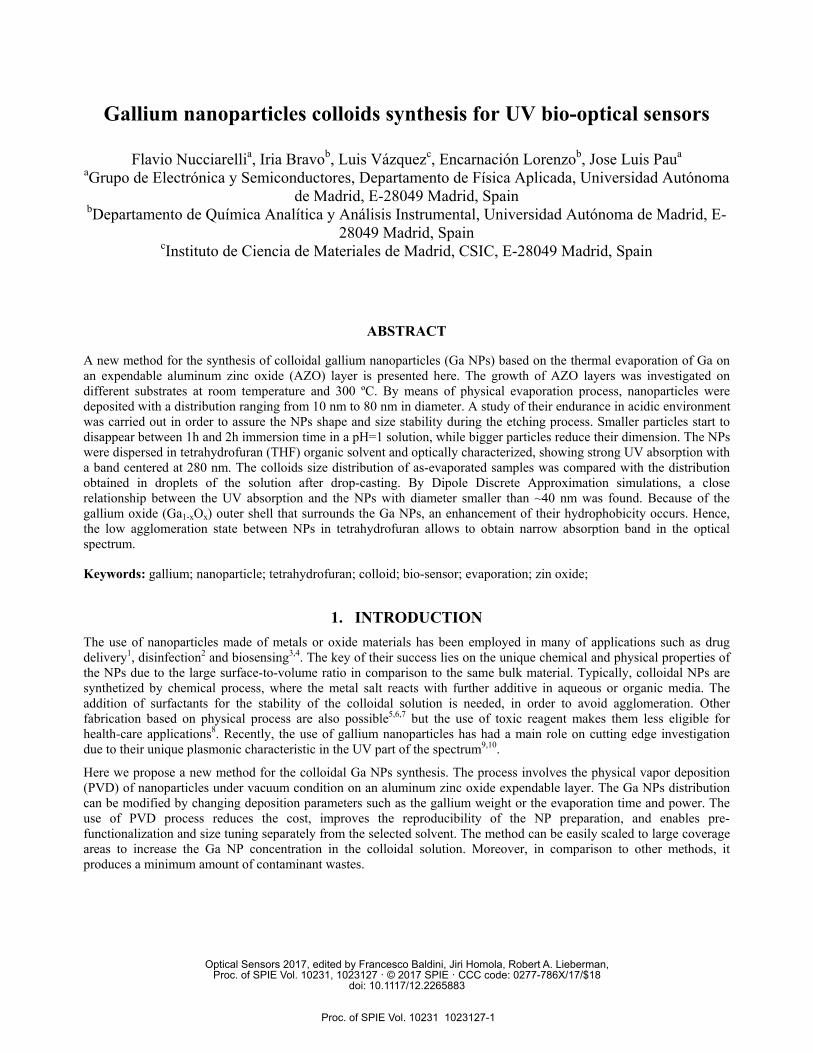
2. EXPERIMENTAL The substrates, Si (100) and glass, with an area of 1 cm2, were cleaned by immersion for 1 minute in an aqueous solution of 40 % fluorhydric acid and acetone respectively. The aluminum zinc oxide expendable layer was deposited on both substrates by an Alcatel A450 RF sputtering equipment. The growth conditions were RF 150 W power, in a 50 sccm Ar flow (10-2 mbar) to sputter the AZO target (ZnO / Al2O3, 2% standard doping) during 10 minutes, both at 300 ºC. Prior to the deposition, the target was sputtered for 1 minute to remove impurities. The thickness of the layer, determined by profilometry, was 300 nm. Atomic force microscopy images show that the grain size depends on the substrate used (figure 1). The expendable layer material was chosen taking into account the following consideration: fast etching in moderately acidic solutions compatible with Ga and a reasonable roughness that does not inhibit the self-assembled mechanism of Ga NPs.
Figure 1. AFM images of the AZO layer at 300 oC grown on (a) silicon and (b) glass
Gallium NPs were evaporated on the sample with the use of a Joule-effect Edwards E306 evaporation system. For our process, 0.28 g of solid Ga (99.999999% purity) was heated for 30 seconds with a 50 W DC power under 10-6 Torr vacuum pressure. The sample were positioned 20 cm far from the Ga crucible and an ice cooling system was used. It helped to keep the substrate temperature as low as possible to limit the metal surface mobility during the nucleation process. The lower the mobility the smaller the NPs can grow without coarsening.
To prepare the colloidal solutions, several vials of 3 ml volume were filled with tetrahydrofuran organic solvent. The THF was chosen because of its peculiar chemical properties, in order to study the colloidal optical absorption. After Ga deposition and extraction from the evaporation system, the sample was immersed in a phosphoric acid/acetic acid/deionized water (1:1:75) bath to etch the AZO layer and weaken the NPs bonds with the substrate, rinsed in water and promptly inserted into the selected solvent. Finally, an ultrasound treatment for 90 seconds was used to release NPs from the hard support and let them be dispersed into the liquid.
In order to characterize the sputtered AZO layer surface, it was used an Agilent PicoPlus 5500 atomic force microscopy (AFM) operating in dynamic mode. To obtain the microscopy images of the sample instead, it was used a Philips XL30 S-FEG scanning electron microscope under a 10-3 bar vacuum pressure at room temperature. The colloidal solution was drop casted on a clean silicon substrate inside a clean room of class 1000 and promptly analyzed in order to avoid possible contamination effects. The images were analyzed by Gwyddion software to estimate nanoparticles size and distribution14. Regard to the UV/visible colloidal absorption spectra, they were acquired by a Thermo Scientific GO spectrophotometer. For the analysis, colloidal solution was poured in a quartz cuvette using the same colloidal solvent as
(a) (b)
Proc. of SPIE Vol. 10231 1023127-2
.
0 6 ® re.: . ..i .. og . .0004r^,b,*AL
,,¡ilk
4 0*. . ,`@:.. ,
reference. By means of the equipment, temperature was fixed at 25 oC and exposed to a light ranging from 200 nm to 1000 nm in wavelength, with a system resolution of 1 nm.
3. OPTIMIZATION OF GA NANOPARTICLES SYNTHESIS A study of the expendable layer was carried out in order to identify the most appropriate growth conditions for our synthesis. Previous comparison between AZO layer grown on Si and glass substrate was investigated, both at room and 300 oC growth temperature. By the atomic force measurement resulted that the high temperature process allowed bigger grain size for both substrates, yielding a more uniform etching of the expendable layer. Figure 1 shows the AFM images of the AZO layer grown on Si and glass at 300 oC. The silicon sample exhibits bigger grain size compared to the glass one and the measured average roughness were 13.6 nm and 9.2 nm, respectively. The higher the roughness, the bigger the surface area on which the Ga NPs may grow leading to higher yield.
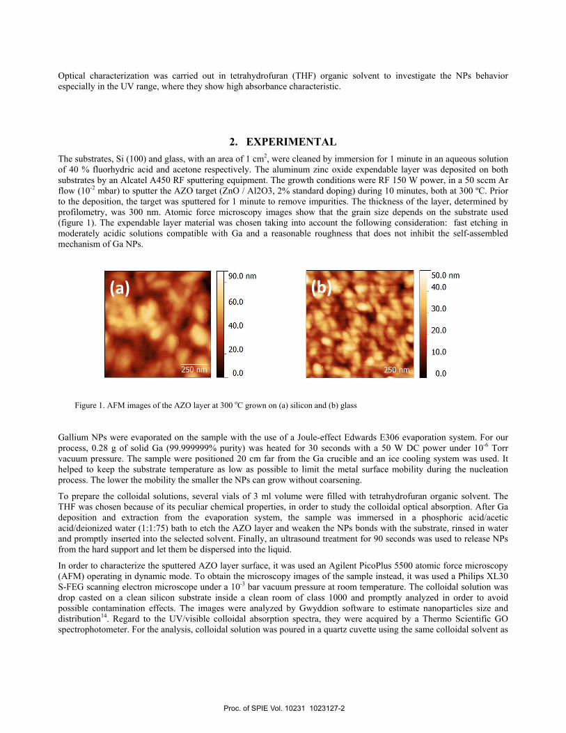
In addition, the effect of acidic environment on Ga NPs was investigated for 1 minute, 1h, 2h and 8h etching times. The NPs were evaporated on a bare glass substrate without AZO layer and immersed in phosphoric acid/acetic acid/deionized water solution (pH=1). The NPs size distribution did not change for etching times shorter than a few minutes and remain the same of the un-etched case (figure 2.a). For longer times instead (figure2.b), particles with smaller radius start to disappear and bigger particles reduce their size. Since the Ga NPs are surrounded by a thin (1-3 nm) oxide shell13, their endurance depends of the chemical stability of the gallium oxide and the metal gallium under acidic environment. The outer oxide may dissolve in a few minutes11, while metal gallium is supposed to be slightly affected by the acids. But a new oxide shell constantly replaces the preexisting dissolved layer and as time passes the inner metal gallium reduces its volume until it totally disappears. For this reason, the etching process in our synthesis has been kept under 1 minute, in order to avoid possible damages or changes in the NPs morphology.
Figure 2. SEM images of Ga NPs evaporated on bare glass: (a) un-etched and (b) 2 h etched. Most of the small NPs disappear after etching creating a different size distribution. Images bars are 1 µm long.
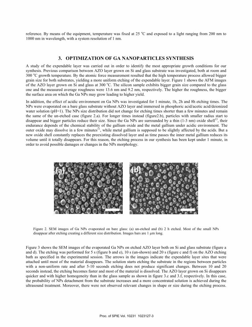
Figure 3 shows the SEM images of the evaporated Ga NPs on etched AZO layer both on Si and glass substrate (figure a and d). The etching was performed for 5 s (figure b and e), 10 s (un-shown) and 20 s (figure c and f) on the AZO etching bath as specified in the experimental session. The arrows in the images indicate the expendable layer sites that were attached until most of the material disappears. The solution starts etching the substrate in the regions between particles with a non-uniform rate and after 5-10 seconds etching does not produce significant changes. Between 10 and 20 seconds instead, the etching becomes faster and most of the material is dissolved. The AZO layer grown on Si disappears quicker and with higher homogeneity than in the glass sample as shown in figure 3.c and 3.f, respectively. In this case, the probability of NPs detachment from the substrate increases and a more concentrated solution is achieved during the ultrasound treatment. Moreover, there were not observed relevant changes in shape or size during the etching process.
(a) (b)
Proc. of SPIE Vol. 10231 1023127-3
Notably, as both images c and f show, the particle have a hemispherical shape. Considering these results, the sample with NPs on AZO layer grown on Si substrate has been demonstrated the most suitable choice to assure higher yield and reproducibility of our colloidal synthesis.
Figure 3. SEM images of Ga NPs on etched AZO layer for different times and substrates. On Si: (a) as-grown, (b) 5 s etched, (c) 20 s etched. On glass: (d) as-grown, (e) 5 s etched, (f) 20 s etched. Arrows mark the etched regions of the AZO layer. Images bars are 200 nm long.
4. OPTICAL ABSORPTION OF GA NANOPARTICLES After the process optimization, Ga NPs colloids in THF solution were prepared and optically characterized. The stability of dispersed particles in a solution is influenced by their agglomeration state, which is mainly related to two factors: the NP/liquid interface and the specific chemical properties of the used solvent. In order to compare the size distribution of the as-grown Ga/AZO/Si sample and a drop-casted sample taken from the colloidal solution, SEM images were taken in both cases. As shown in Figure 4.a and b both samples have similar shape and dimension. Indeed, the NPs size is mostly preserved and higher occurrence of particles between 50 and 100 nm has been found. The reason of the increase for that specific range can be related to possible NPs breaking, while they separate from the substrate. During the detachment, the broken particles divide in smaller ones causing a reduction of the bigger NPs in the drop-casted distribution (bigger than 100 nm). Furthermore, SEM investigation reveals that, in the case of gallium on AZO, the NPs have a hemi-spherical structure similar to the one shown in Figure 2.f. Depending on the growth surface wettability of the evaporated material, nucleation process can change and give different NP shape14. When the NPs get in contact with oxygen, an outer oxide shell covers the metal core and preserves the obtained geometry.
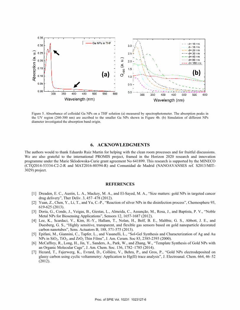
Optical characterization on THF colloidal Ga NPs sample was carried out in the UV/visible range. Because of the high absorption of THF solvent at wavelengths smaller than 220 nm, only the data for values above of 250 nm were considered reliable. The colloid absorption (figure 5.a) shows a well-defined band between 260-300 nm with two peaks centered at 273 nm and 285 nm likely related to the broadening of the NPs size distribution. The narrow absorption of the colloidal solution suggests that nanoparticles are in a low agglomeration state. Their stability may depend on the hydrophobic oxide shell which allows good stability in THF solvent, as other groups have already investigated12. In order to correlate the absorption band with the colloidal Ga NPs distribution, samples with different evaporation time were synthetized. As expected, an enhancement of the absorption was obtained for higher NPs concentration in the solution.
On Si
On Glass
d
ba b c
d e f f
a
d e
cb
Proc. of SPIE Vol. 10231 1023127-4

55 , . , ,
50 {
45
40
2F
,c_i, 30
n 25
Z 2015
10
5
0 50 100 150 200 250 300 350
Diameter (nm)
55
50 Drop -casted Ga NPs
45
40
\°iZ 20
15
10
50 100 150 200 250 300 350
Diameter (nm)
The contribution of the different NPs sizes on the light absorption was theoretically studied through discrete-dipole approximation made with DDSCAT software15. The simulated structures were liquid gallium hemispheres surrounded by 1 nm native oxide shell in THF solvent. The optical constants of the metal and oxide were taken from Knight et al.13 and Rebiena et al.16. The NPs diameter ranged between 10 to 160 nm in order to reproduce the physical properties of the NPs found in the drop-casted sample. The studied wavelength range spans from 255 nm to 800 nm. The simulation considers a circular polarized light beam impinging on the particle. Interaction cutoff parameter was set as high as possible with a value of 3*103, with an error tolerance of 10-4. Figure 5.b shows the absorption efficiency (QABS) which depends of the target cross sectional area. Interestingly, the 30 nm diameter structure shows the highest absorption compared to the rest of structures. This is because QABS is directly proportional to the particle radius while QSCAT is proportional to the forth power of it. This behavior makes possible to obtain an optimum NP size to achieve high absorption and low scattering. The NPs smaller than 40 nm exhibit a well-defined single peak resonance located in the UV region, while, for bigger particles, absorption bands are present along the whole range. Hence, the bigger the structure the less it absorbs in the IR range, due to an increase of scattered light. For this reason, the measured colloidal absorption band was ascribed to NPs smaller than 40 nm and bigger particles do not play a primary role in shaping the absorption. It is possible that NPs larger than 40 nm may be responsible of the bumped absorption area between 300 and 500 nm showed in the experimental colloidal spectrum.
Figure 4. SEM images and the corresponding histograms of (a) as-grown Ga NPs and (b) drop-casted NPs on Si. Images bars are 1 µm long.
5. CONCLUSION In this work, we have proposed a new method to synthetize colloidal Ga NPs in THF solution. The inner metal makes the nanoparticles endure up to some hours before to completely dissolve due to oxidation process between the nanoparticle and the surrounding medium. Notable strong absorption in the UV range was measured for the colloidal in THF solution, which makes our sample eligible for a wide range of application in the (bio)sensors field. The measured absorption band was correlated with the obtained gallium nanoparticle distribution using DDA simulations. It was observed that nanoparticles with diameters smaller than 40 nm may be responsible of the characteristic absorption of our colloids. With this particular colloidal preparation method, most of the chemical processing drawbacks such as low process success and additive contamination are overcome. Nonetheless, the nanoparticles transferred from a hard substrate to the chosen solvent allows their previous functionalization by ion implantation or chemical and thermal treatments. Finally, as demonstrated in previous works, it is possible to functionalize the solution with thiols through the formation of S-Ga bonds, which opens the possibility of developing high sensitivity systems for molecular imaging in combination with DNA and biological sensor in a broad range of applications.
(a) (b)
Proc. of SPIE Vol. 10231 1023127-5
035
Ga NPs in THE
0.25
1.5
1 . 0 - - ---- --------------_ _ _
""
0.0300 350 400 450 500 550 600
Wavelength (nm)
cd020
o0.15
ñ
o.oU.US
0 .00300 350 400 450 500 550 600
Wavelength (nm)
3.0d=10nm
1
2.5
a= io nm-- d= 20 nm-- - - - d= 30 nm
A,2.0 d= 80 nm
d= 160 nm
Figure 5. Absorbance of colloidal Ga NPs on a THF solution (a) measured by spectrophotometer. The absorption peaks in the UV region (260-300 nm) are ascribed to the smaller Ga NPs shown in Figure 4b. (b) Simulation of different NPs diameter investigated the absorption band origin.
6. ACKNOWLEDGMENTSThe authors would to thank Eduardo Ruiz Martin for helping with the clean room processes and for fruitful discussions. We are also grateful to the international PROMIS project, framed in the Horizon 2020 research and innovation programme under the Marie Sklodowska-Curie grant agreement No 641899. This research is supported by the MINECO (CTQ2014-53334-C2-2-R and MAT2016-80394-R) and Comunidad de Madrid (NANOAVANSES ref. S2013/MIT-3029) project.
REFERENCES
[1] Dreaden, E. C., Austin, L. A., Mackey, M. A., and El-Sayed, M. A., “Size matters: gold NPs in targeted cancerdrug delivery”, Ther Deliv. 3, 457–478 (2012).
[2] Yuan, Z., Chen, Y., Li, T., and Yu, C.-P., “Reaction of silver NPs in the disinfection process”, Chemosphere 93,619-625 (2013).
[3] Doria, G., Conde, J., Veigas, B., Giestas, L., Almeida, C., Assunção, M., Rosa, J., and Baptista, P. V., “NobleMetal NPs for Biosensing Applications”, Sensors 12, 1657-1687 (2012).
[4] Lee, K., Scardaci, V., Kim, H.-Y., Hallam, T., Nolan, H., Bolf, B. E., Maltbie, G. S., Abbott, J. E., andDuesberg, G. S., “Highly sensitive, transparent, and flexible gas sensors based on gold nanoparticle decoratedcarbon nanotubes”, Sens. Actuators B, 188, 571-575 (2013).
[5] Epifani, M., Giannini, C., Tapfer, L., and Vasanelli, L., “Sol-Gel Synthesis and Characterization of Ag and AuNPs in SiO2, TiO2, and ZrO2 Thin Films”, J. Am. Ceram. Soc 83, 2385-2393 (2000).
[6] McCaffrey, R., Long, H., Jin, Y., Sanders, A., Park, W., and Zhang, W., “Template Synthesis of Gold NPs withan Organic Molecular Cage”, J. Am. Chem. Soc. 136, 1782–1785 (2014).
[7] Hezard, T., Fajerwerg, K., Evrard, D., Collière, V., Behra, P., and Gros, P., “Gold NPs electrodeposited onglassy carbon using cyclic voltammetry: Application to Hg(II) trace analysis”, J. Electroanal. Chem. 664, 46–52(2012).
(a) (b)
Proc. of SPIE Vol. 10231 1023127-6
[8] Bhau, B. S., Ghosh, S., Puri, S., Borah, B., Sarmah, D. K., and Khan, R., “Green synthesis of gold NPs from the leaf extract of Nepenthes khasiana and antimicrobial assay”, Adv. Mater. Lett. 6, 55-58 (2015).
[9] Meléndrez, M. F., Cárdenas, G., and Arbiol, J., “Synthesis and characterization of gallium colloidal NPs”, J. Colloid Interface Sci. 346, 279–287 (2010).
[10] Yarema, M., Wörle, M., Rossell, M. D., Erni, R., Caputo, R., Protesescu, L., Kravchyk, K. V., Dirin, D. N., Lienau, K., Rohr, F., Schilling, A., Nachtegaal, M., and Kovalenko, M. V., “Monodisperse Colloidal Gallium NPs: Synthesis, Low Temperature Crystallization, Surface Plasmon Resonance and Li-Ion Storage”, J. Am. Chem. Soc. 136, 12422−12430 (2014).
[11] Ohira, S. and Arai, N., “Wet chemical etching behavior of β-Ga2O3 single crystal”, phys. stat. sol. (c) 5 No. 9 3116–3118 (2008)
[12] Vasiliev, A. N., Gulliver, E. A., Khinast, J. G., Riman, R. E., “Highly dispersible polymer-coated silver Nanoparticle”, SURF COAT TECH 203 2841–2844 (2009)
[13] Knight, M.W. et al., “Gallium Plasmonics: Deep Subwavelength Spectroscopic Imaging of Single and Interacting Gallium Nanoparticles”, ACS Nano VOL. 9 NO. 2 2049–2060 (2015)
[14] Necas, D., Klapetek, P., “Gwyddion: an open-source software for SPM data analysis”, Cent. Eur. J. Phys. 10(1) 181-188 (2012)
[15] Draine, B.T. and Flatau, P.J., “Discrete dipole approximation for scattering calculations”, J. Opt. Soc. Am. A, 11, 1491-1499 (1994)
[16] Rebiena, M., Henrion, W., Hong, M., Mannaerts, J. P., and Fleischer, M., “Optical properties of gallium oxide thin films”, Appl. Phys. Lett. Vol. 81, No. 2, 8 July (2002)
Proc. of SPIE Vol. 10231 1023127-7