Gain/loss characterisation of optical waveguide and semiconductor laser structures
6
Gain/loss characterisation of optical waveguide and semiconductor laser structures C.Themistos A. Hadjicharalambous B.M.A. Rahman K.T.V. Grattan F.A. Fernandez Indexing terms: Modal gain analysis, Finite eketnmt method, Perturbation techniques, MQ W lasers ... Abstract: Finite element analysis, employing the H-field vector and scalar formulations, has been used with the aid of perturbation techniques to determine the modal gain and loss characteristics of optical waveguides and semiconductor laser structures. The accuracy and the applicability limits of the perturbation method are examined, and compared to the more accurate but more computer intensive transverse magnetic field formulation for an embedded-channel waveguide. Further, the method is applied to a rib-waveguide laser structure, where the imaginary part of the refractive index of the InGaAsP active layer is seen to vary according to the carrier concentration profile. Finally, the accuracy of a widely used but simpler method for determining the modal gain for QW and MQW laser structures, in terms of the optical mode confinement, is determined. 1 Introduction The use of the finite element method for the analysis of optical waveguide characteristics is widely recognised as a very powerful technique, particularly for structures with arbitrary shapes, index profiles, nonlinearities and anisotropies. Most of the formulations used in the finite element method (FEM), such as the scalar [l], EJH, [2] and H- field formulations [3], are restricted in their applica- tions to structures without modal loss or gain. Due to the necessity for the analysis of practical optical waveguides which suffer small or medium modal loss or gain, various different techniques have been devel- oped. The approaches applicable to the use of the FEM are to yield the vector solution in terms of the transverse magnetic field vector (H, formulation) as ~~ ~ 0 IEE, 1998 IEE Proceedings online no. 19981674 Paper first received 23rd April and in revised form 25th September 1997 C. Themistos. A. Hadjicharalambous, B.M.A. Rahman and K.T.V. Grat- tan are with the Measurement and Instrumentation Centre, Department of Electrical, Electronic and Information Engineering, City University, Northampton Square, London ECI OHB, UK F.A. Femandez is with the University College, London WClE 7JE, UK reported in previous work by several authors [4-61, and the use of the perturbation technique which has been successfully applied to scalar [7, 81 and full vector H- field formulations [9]. In the H, formulation, the modal loss or gain is directly calculated from the solution of the complex eigenvalue equation and does not yield spurious solutions. In this case there are two unknown field components instead of three, and the size of the original global matrices is thereby reduced as compared to the full H-field formulation. This efficient H, formulation does not sacrifice the sparsity of the resultant matrices and is supported by an efficient sparse matrix solver which can solve large problems on a medium-sized workstation. The above method is compared with the full vector H formulation with perturbation, in terms of mesh size, the modal gain/loss accuracy limit and field distribution, consid- ered in order to examine the validity of the perturba- tion approximation. 2 effects Finite element method including perturbation In using the FEM method, the cross section of the optical waveguide in the transverse x-y plane is divided into a patchwork of triangular elements of different sizes, shapes, refractive indices and anisotropies. The field distribution in the transverse plane is obtained by the application of the variational formulation in the region. The usual time and axial dependencies are given by expQwt) and exp(-y), respectively, for angular fre- quency w and time t, where y= a + jj3, is the complex propagation constant in the z direction, and /3 and a are the phase and attenuation constants, respectively. Previously, perturbation techniques have been applied to the estimation of losdgain parameters of the optical waveguides, in conjunction with the scalar finite element method for both the TE and TM modes [8] and the H-field formulation [9], in applications to problems with small loss/gain. In such cases the per- turbed fields were approximated by those fields obtained by solving the variational formulation using only the real part of the dielectric constant. The attenu- ation constant was then calculated from the results obtained from the loss-free system by using simple matrix multiplication. The detailed calculations for the scalar and the vector H-field variational formulation with perturbation, used in the present work, are given in the [8] and [9], respectively. 93 IEE Proc.-Oproelr~tron.. Vol. 145, No. 2, April 199X
Transcript of Gain/loss characterisation of optical waveguide and semiconductor laser structures
Gain/loss characterisation of optical waveguide and semiconductor laser structures
C.Themistos A. Hadjicharalambous B.M.A. Rahman K.T.V. Grattan F.A. Fernandez
Indexing terms: Modal gain analysis, Finite eketnmt method, Perturbation techniques, MQ W lasers ...
Abstract: Finite element analysis, employing the H-field vector and scalar formulations, has been used with the aid of perturbation techniques to determine the modal gain and loss characteristics of optical waveguides and semiconductor laser structures. The accuracy and the applicability limits of the perturbation method are examined, and compared to the more accurate but more computer intensive transverse magnetic field formulation for an embedded-channel waveguide. Further, the method is applied to a rib-waveguide laser structure, where the imaginary part of the refractive index of the InGaAsP active layer is seen to vary according to the carrier concentration profile. Finally, the accuracy of a widely used but simpler method for determining the modal gain for QW and MQW laser structures, in terms of the optical mode confinement, is determined.
1 Introduction
The use of the finite element method for the analysis of optical waveguide characteristics is widely recognised as a very powerful technique, particularly for structures with arbitrary shapes, index profiles, nonlinearities and anisotropies.
Most of the formulations used in the finite element method (FEM), such as the scalar [l], EJH, [2] and H- field formulations [3], are restricted in their applica- tions to structures without modal loss or gain. Due to the necessity for the analysis of practical optical waveguides which suffer small or medium modal loss or gain, various different techniques have been devel- oped. The approaches applicable to the use of the FEM are to yield the vector solution in terms of the transverse magnetic field vector (H, formulation) as
~~ ~
0 IEE, 1998 IEE Proceedings online no. 19981674 Paper first received 23rd April and in revised form 25th September 1997 C. Themistos. A. Hadjicharalambous, B.M.A. Rahman and K.T.V. Grat- tan are with the Measurement and Instrumentation Centre, Department of Electrical, Electronic and Information Engineering, City University, Northampton Square, London ECI OHB, UK F.A. Femandez is with the University College, London WClE 7JE, UK
reported in previous work by several authors [4-61, and the use of the perturbation technique which has been successfully applied to scalar [7, 81 and full vector H- field formulations [9]. In the H, formulation, the modal loss or gain is directly calculated from the solution of the complex eigenvalue equation and does not yield spurious solutions. In this case there are two unknown field components instead of three, and the size of the original global matrices is thereby reduced as compared to the full H-field formulation.
This efficient H, formulation does not sacrifice the sparsity of the resultant matrices and is supported by an efficient sparse matrix solver which can solve large problems on a medium-sized workstation. The above method is compared with the full vector H formulation with perturbation, in terms of mesh size, the modal gain/loss accuracy limit and field distribution, consid- ered in order to examine the validity of the perturba- tion approximation.
2 effects
Finite element method including perturbation
In using the FEM method, the cross section of the optical waveguide in the transverse x-y plane is divided into a patchwork of triangular elements of different sizes, shapes, refractive indices and anisotropies. The field distribution in the transverse plane is obtained by the application of the variational formulation in the region. The usual time and axial dependencies are given by expQwt) and exp(-y), respectively, for angular fre- quency w and time t , where y = a + jj3, is the complex propagation constant in the z direction, and /3 and a are the phase and attenuation constants, respectively.
Previously, perturbation techniques have been applied to the estimation of losdgain parameters of the optical waveguides, in conjunction with the scalar finite element method for both the TE and TM modes [8] and the H-field formulation [9], in applications to problems with small loss/gain. In such cases the per- turbed fields were approximated by those fields obtained by solving the variational formulation using only the real part of the dielectric constant. The attenu- ation constant was then calculated from the results obtained from the loss-free system by using simple matrix multiplication. The detailed calculations for the scalar and the vector H-field variational formulation with perturbation, used in the present work, are given in the [8] and [9], respectively.
93 IEE Proc.-Oproelr~tron.. Vol. 145, No. 2, April 199X

3 Dependence of refractive index on carrier concentration
A knowledge of the device material properties is funda- mental to modelling semiconductor optoelectronic components. The measured data for the device material in semiconductor lasers and laser amplifiers, such as the gain, carrier lifetime and refractive index and their dependence on the injected carrier density, are very important in predicting the associated laser properties. The carrier concentration profile N(x, y ) in a laser material, which is dependent on the injected current, determines the change of the complex refractive index profile n(x, y) .
InGaAsP lasers enable the exploitation of the mini- mum loss in silica-based optical communication sys- tems at their operating wavelength of il = 1.55pm. A rib waveguide with an active layer of InGaAsP laser material at the above operating wavelength has been examined in order to calculate the gain properties of the structure. Since the small loss condition is exam- ined, the effect of the carrier concentration on the real part of the refractive index has been neglected. The variation of the imaginary part of the refractive index n" along the transverse direction x is related to the car- rier variation N(x) and is given by
dn dN
n y x ) = -N(z )
where dnidN is the rate of-change of the refractive index with carrier concentration, and N(x) the carrier concentration profile given by [lo]:
(2) X l S i No sinh(s/ l ) exp(-z/L) n: > s
cosh(z/L) No (1 - w) N ( x ) =
No is the carrier concentration at threshold, s is the half rib width and L the diffusion length.
The average carrier concentration within the active layer, which represents an active layer with uniform carrier concentration, can be approximated by averag- ing the carrier profile along the x-axis as
1 hw Na, = LJ, N(x)dn: = (s/hw)No ( 3 )
where h, is the half-guide width, which is assumed large compared to the half-rib width s, as shown in Fig. 1.
I S
! * .................., I I 4
! I t ! n=3.17+jO
active region
...... n =3.38+jn", InGaAsP ,-
substrate
! ...........................................................
I hw 'X
I
A
/ t
i
Fig. 1 tive index in the active layer varies according to the carrier profie
Rib waveguide structure where the imaginary part of the refiac-
4 Approximate relationship between modal gain and confinement factor
It can be shown that the modal gain g, for a well con- fined mode in a simple optical waveguide structure incorporating an active region can be approxiinated by
gm = n//lcor (4) where n" is the imaginary part of the refractive index in the active region, k , is the wavenumber and r is the power confinement factor given by
r = Pactzae l a y e r l p g u i d e (5) P above is the power in a given region Q, and defined by
P = Re x H;)2dfl ( 6 )
where E,, Ho* and Q are the electric field, the conjugate of the magnetic field and the cross-section of the guide region respectively.
Eqn. 4 provides a relatively easy way of estimating the gainiloss properties of a waveguide in terms of the confinement factor. It can also be extended to struc- tures with many active layers, each having a different imaginary part of the refractive index, as follows:
L
gm = ko x Cn:rz (7 ) 7,=1
where L is the number of active layers, nl" is the imagi- nary part of the refractive index which can take posi- tive or negative values depending on whether there is gain or loss and Ti is the confinement factor of each layer.
The accuracy of this approach can also be examined by applying it in different types of optical waveguides.
5 Results of simulation
The validity of the scalar and vector FEM, with respect to the H, formulation and the complex Effective Index Method (EIM), has been tested for a GaInAsPAnP embedded rectangular channel (of width w = 5d, where d is the height of the core), with core and substrate refractive indices respectively given by n1 = 3.5 + jO.001 and n2 = 3.2 - J O (lossless substrate), where the wave- number ko is normalised to 1.
The variation of the effective indices and modal gain (or loss) for the fundamental quasi TE (Hy,,) mode with the total element number is shown in Fig. 2, for various numerical approaches used in this work. In the H, approach, Maxwell's equations are solved with finite elements in terms of the transverse field compo- nents, with the use of an efficient complex sparse matrix solver, yielding no spurious solutions. In the vector H-field (H) and the Scalar (S) approaches, the solutions obtained, with the aid of an efficient sparse,
junction with the perturbation technique (P) to calcu- late the modal gain (or loss) properties. In the effective index method (EIM), the solution of the complex tran- scendental equation is obtained iteratively [9] to calcu- late the complex propagation constant.
It can be observed that as the number of elements is increased, the modal solution is seen to converge. When the number of elements is 1800, the effective index values (n,) obtained by the H, and vector (V + P) approaches, agree well. For the above mesh representa-
real matrix solver for the lossless case, are used in con-
IEE Proc -0ptoelectron.. Vol. 145. No. 2, April 1998 94

’ tion, the Scalar approach (S + P) and the EIM, which is analytical and does not depend on the mesh size, overestimate the effective index ne by about 0.001, com- pared to the more accurate H, and the vector (V + P) approaches. Since a lossless substrate is assumed in the above case, the normalised attenuation constant, a/ko can take negative values, indicating modal gain in the waveguide, and can be expressed in terms of the nor- malised gain constant glk,, where g = -a. The modal gain characteristics, also shown in Fig. 2, demonstrate similar behaviour with the effective index curves for the above methods. In this case, with 1800 elements, the EIM and the scalar (S + P) methods overestimate the factor g/ko, by 0.005 (about 434dB/cm), compared to the H t and the vector (V + P) approaches.
1 0.77 3.35 I I , I I0.75
200 400 600 800 1000 1200 1400 1600 1800
elements
Fig.2 Variation ofthe effective index (n ) and the normalizedgain con- stant ( &) with the mesh division of an‘embedded channel waveguide, using tt& Ht, the vector H-jkld with perturbation ( V + P) and the scalar H-field with perturbation ( S i P ) finite element formulations and the com- plex ejjective index method ( E I M ) - H , ; . . . V + P ; - - - - S + P ; - . - E I M
The Ht program was executed on a remote worksta- tion using object code and appeared to take much longer in execution. It can be noted that for 1800 ele- ments, the execution time is about 25s on a Sun Classic Sparcstation for the vector (V + P) solution. It can also be noted from Fig. 2, that to obtain satisfactory modal solutions at least 1000 first order elements need to be used.
3.40 I j 100000
3.38
3.36
3.34
3.32
ca 3.30
3.28
3.26
3.22 3’24 1
10000
5 $ m
1000
1 n;=0
3.20 I 4 1 1 1 100 0.01 0.1 1
n,“
~ H . . . . . . v+p; ~ - - - EIM
Next, the modal gain is varied by changing the imag- inary part of the core refractive index nnl to check the limit of the perturbation technique, while the substrate was again considered lossless (nn2 = 0). Fig. 3 shows the comparison of the EIM, the vector H method with perturbation (V + P) and the H, method, for the varia- tion of the imaginary part of the refractive index nr” as far as the effective index and the modal gain are con- cerned. In this particular case, 1800 first order elements were used to represent the waveguide structure. The gain constant g curves agree well for the V + P and H, approach and slowly diverge only when the value of g is larger than 10000dB/cm. The EIM fails to converge [SI for values of n l” above 0.06 and the numerical pro- cedure becomes unstable. The vector H method and the H , method begin to diverge, for both the effective index and modal gain, at a value of n l” = 0.1.
An integrated laser rib waveguide with an lnGaAsP active layer, at an operating wavelength of A = 1.5pm, has been examined, as shown in Fig. 1. The imaginary part of the refractive index in the active region is con- sidered to vary according to the carrier concentration profile along the x-axis (eqn. 2). The carrier concentra- tion at threshold is assumed to be No = 1.0 * 10’8cm-3, and dnidN is -2.8 * 10-20cm3 [lo]. For this example, the rib width is considered to be 5 p n and the existing one- fold symmetry has been exploited in the numerical sim- ulation. From the above data, the carrier distribution in the active layer is plotted in Fig. 4, for two different diffusion lengths, L = 1 . 2 ~ and L = 1.7pn. For the smaller diffusion length L = 1.2pn, the carrier concen- tration is higher in the centre rib region, and lower out- side, and for both distributions the carrier values are identical at the end of the rib. The average carrier dis- tribution N,, (eqn. 3) is plotted in the same figure, and it has a value of about 25% of the maximum carrier concentration ( 10i8cm-?). This value corresponds to the ratio of the rib half width (s = 2 . 5 ~ ) to the guide half width (h , = 2 0 p ) , as defined by (eqn. 3) .
0.8
h m
0
? 0.6 25
E 0.4 -
2
0.2
I I I I
- 0 1 2 3 4 5 x, pm
Fig. 4 Currier projik along the x-axis iri the active layer of’ the rib sem- iconductor laser optical waveguide, for diflerent values oj the dflusion length L of the carrier
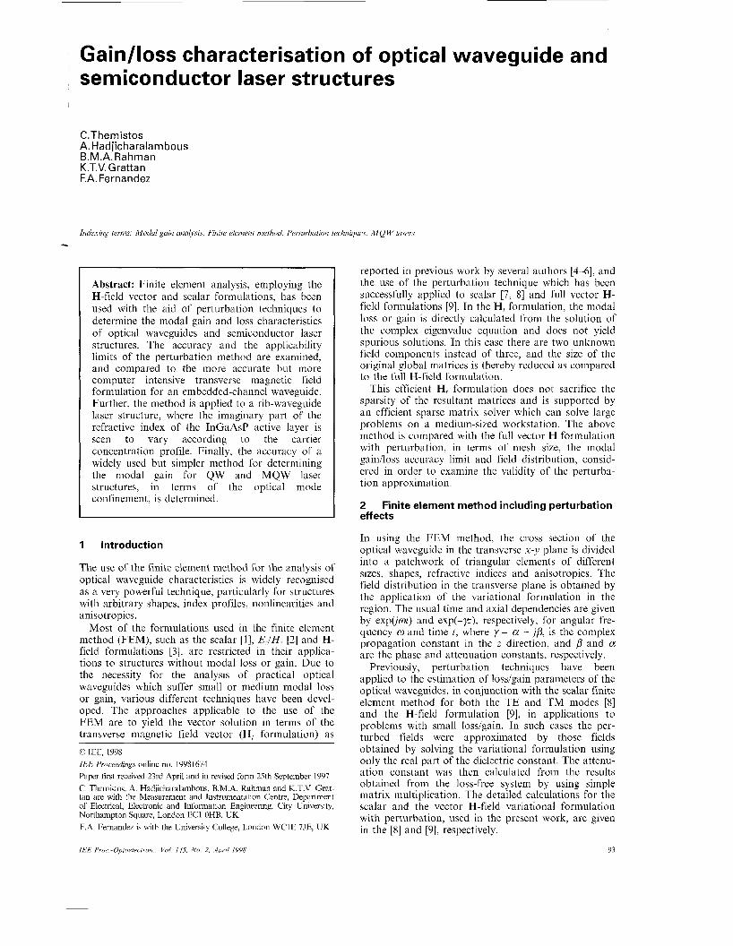
In addition, the modal gain for the two diffusion lengths is shown in Fig. 5 with respect to the threshold carrier concentration No. As No increases the modal gain is seen to increase. For a smaller diffusion length, the modal gain is higher than that of the larger dlffu- sion length, since in the former case the carriers are more concentrated near the guide centre where the optical field intensity is also higher. In the EIM model
95 IEE Proc.-Optoelectron., Vol. 145, No. 2, April 1998
it may not be possible to consider the spatial variation of the carrier or the local gain, so a comparison is made considering uniform concentration of the carrier. The modal gain for the average carrier concentration is lower, and is independent of the diffusion length.
1000 L I
10 1.0 1.2 1.4 1.6 1.8 2.0 2.2 2.4 2.6 2.8 3.0
No, cm (x10 ) -3 18
Fig.5 Viiriation of the niodal gain constant for the rib semiconductor luser waveguide with the carrier concentration at threshold No of the active layer, ,for dijjerent values of the @fusion length of the carrier
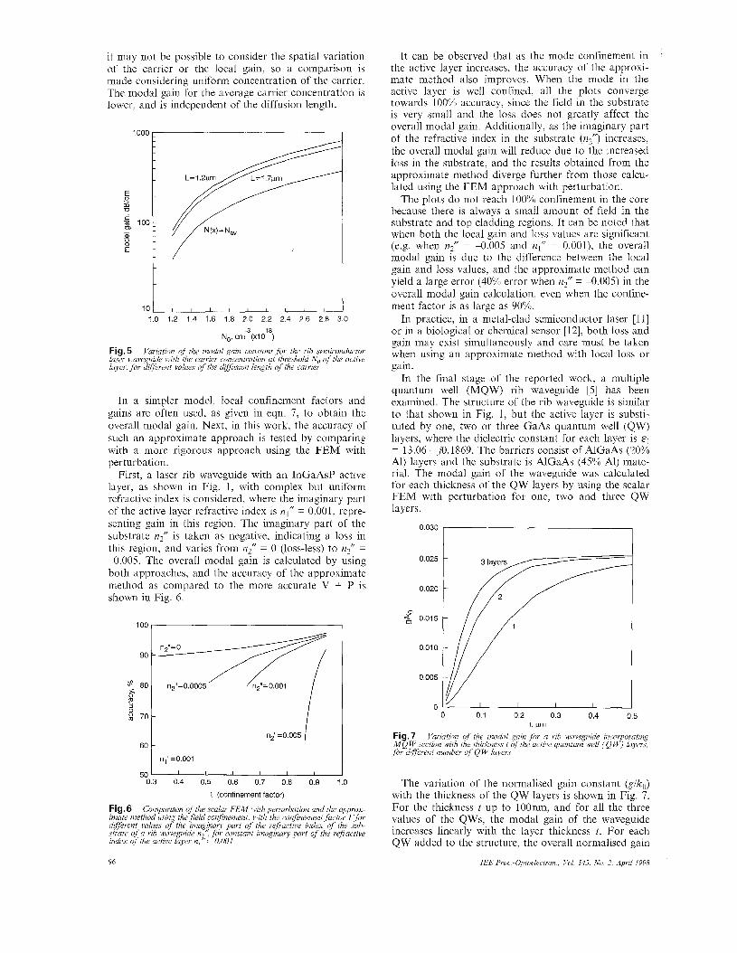
In a simpler model, local confinement factors and gains are often used, as given in eqn. 7, to obtain the overall modal gain. Next, in this work, the accuracy of such an approximate approach is tested by comparing with a more rigorous approach using the FEM with perturbation.
First, a laser rib waveguide with an InGaAsP active layer, as shown in Fig. 1, with complex but uniform refractive index is considered, where the imaginary part of the active layer refractive index is nl” = 0.001, repre- senting gain in this region. The imaginary part of the substrate n; is taken as negative, indicating a loss in this region, and varies from yl; = 0 (loss-less) to n; = -0.005. The overall modal gain is calculated by using both approaches, and the accuracy of the approximate method as compared to the more accurate V + P is shown in Fig. 6.
100,
n2”= 0.00 1
90
2 80 - n;=0.0005
n;=0.005 I
I I I I I I
0.3 0.4 0.5 0.6 0.7 0.8 0.9 1.0
r (confinement factor)
Fig. 6 Comparison of the scalar FEM with perturbation cind the approx- imate nzethod using the field confinement, with the confinement factor l- for dqjerent values of the imagginary part of the refractive index of the sub- strate of U rib wuveguide n ’( for constant imaginary part of the rejiactive index ofthe active layer 0.001
It can be observed that as the mode confinement in the active layer increases, the accuracy of the approxi- mate method also improves. When the mode in the active layer is well confined, all the plots converge towards 100% accuracy, since the field in the substrate is very small and the loss does not greatly affect the overall modal gain. Additionally, as the imaginary part of the refractive index in the substrate (n;) increases, the overall modal gain will reduce due to the increased loss in the substrate, and the results obtained from the approximate method diverge further from those calcu- lated using the FEM approach with perturbation.
The plots do not reach 100% confinement in the core because there is always a small amount of field in the substrate and top cladding regions. It can be noted that when both the local gain and loss values are significant (e.g. when Q” = -0.005 and n,” = 0.001), the overall modal gain is due to the difference between the local gain and loss values, and the approximate method can yield a large error (40% error when n: = -0.005) in the overall modal gain calculation, even when the confine- ment factor is as large as 90%.
In practice, in a metal-clad semiconductor laser [ l l ] or in a biological or chemical sensor [12], both loss and gain may exist simultaneously and care must be taken when using an approximate method with local loss or gain.
In the final stage of the reported work, a multiple quantum well (MQW) rib waveguide [SI has been examined. The structure of the rib waveguide is similar to that shown in Fig. 1, but the active layer is substi- tuted by one, two or three GaAs quantum well (QW) layers, where the dielectric constant for each layer is E, = 13.06 -j0.1869. The barriers consist of AlGaAs (20% Al) layers and the substrate is AlGaAs (4%” AI) mate- rial. The modal gain of the waveguide was calculated for each thickness of the QW layers by using the scalar FEM with perturbation for one, two and three QW layers.
0.030
0.025
0.020
0 0.015
0.010
0.005
0 0 0.1 0.2 0.3 0.4 0.5
t, prn
Fig.7 Variation of the modal gain for a rib waveguide incorporating MQ W section with the tliiclcness t of the active quantum well ( Q W ) layers, .for dgjerent number of Q W layers
The variation of the normalised gain constant (g/ko) with the thickness of the QW layers is shown in Fig. 7. For the thickness t up to 100nm, and for all the three values of the QWs, the modal gain of the waveguide increases linearly with the layer thickness t. For each QW added to the structure, the overall normalised gain
IEE Proc -0ptoelectron , Vol 145, No 2 April 1998 96

constant increases by one above that of the normalised gain constant of the single QW structure, and therefore by adding N QWs, the overall modal gain will be N times the modal gain of the single QW structure. In practical applications, the optimum number of QWs required for a particular structure is determined by the threshold current of the device in order to achieve opti- mum efficiency. The normalised gain constant obtained for a thickness of t = l00nm was compared with the value obtained by Cheung et ul. [6] and found to be in very good agreement.
Additionally, a result for the same thickness was obtained by using the Field Confinement Method, and a comparison shows that this was 93.1% of the previ- ous value, although in this case the field confinement in the active region is much lower (7.5%) than in the rib structure examined earlier using the same method. As the thickness increases above a value of t = l00nm there is a rapid rise in the normalised gain constant, while for the two and three layer structures the rate of increase is higher. At about t = 0 . 3 , ~ ~ all the modal gains begin to saturate and converge to a value of 0.025, with the normalised gain constant of the single layer structure converging more slowly.
The increase of the normalised gain constant can be related to the increase of the confinement factor, which for very large thickness is almost loo%, and therefore
*r saturation of the gain occurs. Of course, when the thickness of the active layers is increased very consider- ably the waveguide no longer exhibits the properties of the MQW structure, especially the low threshold cur- rent, and therefore the structure becomes inefficient since a considerable increase of injection current is required to produce stimulated emission.
,
100, I
90 0 0.02 0.04 0.06 0.08 0.1
t, pm Fi 8 Comparison of the accuracy o j the normalised gain constant cul- cu%ions, by using Scalar FEM with perturbation and the a proximate method in terms o con$nement juctor r with the variation of t/e quantum layer ( Q W ) thicLe,m t for dijjerent numbers of qumtum layers of a rib waveguide incorporating a MQ W section
Next, the modal gain for the MQW lasing structure studied above was also calculated using the approxi- mate method, in terms of the mode confinement factor. The two methods were compared for different numbers of active layers in the MQW region for a typical range of QW thickness, as shown in Fig. 8. In this structure the confinement in the active layers is small (of the order of 10’31) as compared to the previous structure examined. However, as the number of the layers and the modal confinement decreases, the agreement
IEE Proc.-Optoelectron.. Vol. 145, N o . 2, April 1998
between the two methods seems to deteriorate. In a practical lasing structure with optical absorption in other regions, the accuracy of the approximate method will deteriorate even further.
6 Conclusions
Results for the complex propagation characteristics of optical waveguides, using the finite element analysis with vector and scalar H-field formulations and the perturbation technique, were obtained and found to agree well for both the effective index (n,), and the gain constant (g ) , for small to medium modal lossigain val- ues, with similar results obtained by using the more rig- orous H, formulation. The limit of the perturbation approach has been investigated, and it has been shown that the accuracy of the complex propagation constant is quite satisfactory for modal gain ranges up to 2000dB/cm, which is acceptable for most practical opti- cal waveguide structures where modal loss or gain is not excessive. The perturbation approach, being com- putationally more efficient, has been used in the subse- quent simulations.
Modal gain was calculated for semiconductor laser structures, where the loss in the active layer was con- sidered to vary according to the carrier profile for dif- ferent diffusion lengths. Carrier density is one of the most important device parameters in a semiconductor laser and the determination of its effect on the optical properties of an optical waveguide is very important, rather than the use of average carrier and homogene- ous active region.
The validity of a widely used but approximate approach has been discussed in the calculation of the attenuationigain constant for several optical waveguides with elements that exhibit loss or gain in their material properties. This was done by using the imaginary part of the refractive index in these regions and the field confinement factor. The approach is quite satisfactory in cases where the field is well confined in the area where there is either gain or loss, but not both. However, when the confinement factor is smaller, or gain and loss exist simultaneously in different regions of the structure, the results obtained using the approxi- mate approach can be unacceptable. Also, this approach is not suitable and becomes difficult to use where gain values are not piecewise constant, but vary continuously in the transverse directions.
7 Acknowledgments
We would like to express our thanks to Dr. H. Hernan- dez for his assistance in using the program for the H, formulation.
8 References
1 MABAYA, N., LAGGASE, P.E., and VANDENBULCKE, P.: ‘Finite element analysis of optical waveguides’, IEEE Trans. M ~ ~ Y o w . Theory Tech., 1981, 29, (6), pp. 600-605
2 YEH, C., HA, K., DONG, S.B., and BROWN, W.P.: ‘Single- mode optical waveguides’, Appl. Opt., 1979, 18, pp. 1490-1504
3 RAHMAN, B.M.A., and DAVIES, J.B.: ‘Finite-element solution of integrated optical waveguides’, J. Lightn.uve Technol., 1984, 2, ( 5 ) , pp. 682-688 LU, Y . , and FERNANDEZ, F.A.: ‘An efficient finite element method of inhomogeneous anisotropic and lossy dielectric waveguides’, IEEE Truns. Microw. Theory Tech., 1993, 41, pp. 1215-1223
5 FERNANDEZ, F.A., and LU, Y.: ‘Microwave and optical waveguide analysis by the finite element method’ (Research Study Press, 1996)
4
97

6 CHEUNG, P., SILVEIRA, M., and GOPINATH, A.: ‘Analysis of lossy dielectric guides by transverse magnetic field’, J. Light- wave Technol., 1995, 13, (9), pp. 1873-1875
7 HAYATA, K., KOSHIBA, M., and SUZUKI, M.: ‘Lateral mode analysis of buried heterostructure diode lasers by the finite- element method’, IEEE J. Quantum Electron., 1986, 22, (6), pp. 781-788
8 THEMISTOS, C,., RAHMAN, B.M.A., and GRAT- TAN, K.T.V.: Finite element analysis for lossy optical waveguides by using perturbation techniques’, IEEE Photonics Technol. Lett., 1994, 6, (4), pp. 537-539
9 THEMISTOS, C., RAHMAN, B.M.A., HADJICHARALAM- BOUS, A., and GRATTAN, K.T.V.: ‘Losdgain characterization of optical waveguides’, J. Lightwave Technol., 1995, 13, (8), pp. 1760-1765
10 WESTBROOK, L.D.: ‘Measurements of dg/dN and dn/dN and their dependence on photon energy in /z = 1.5” InGaAsP laser diodes’, IEE Proc. J , Optoelectron., 1996, 143, ( 2 ) , pp. 135-142
11 BORCHERT, B., and STEGMULLER, G.: ‘Yield analysis of distributed-feedback metal-clad ridge-waveguide laser diodes for coherent system applications’, IEE Proc. J , Optoelectron., 1990, 137, (4), pp. 265-272
12 QING, D.K., CHEN, X.M., ITOH, K., and MURABA- YASHI, M.: ‘A theoretical evaluation of the absorption coeffi- cient of the optical waveguide chemical or biological sensors by group index method’, J Lightwave Technol., 1996, 14, (8), pp. 1907-1 9 17
98 IEE Puoc.-Optorlectron.. Vol. 145, No. 2, April 1998