
G703E1 Installation & Operation · PDF fileG.703 E1 Installation and Operation Manual Version...
62
INSTALLATION and OPERATION MANUAL
Transcript of G703E1 Installation & Operation · PDF fileG.703 E1 Installation and Operation Manual Version...

INSTALLAT ION and
OPERATION MANUAL


CTC Union Technologies Co., Ltd. Far Eastern Edison Science and Technology Center 6F-3, No. 15, Lane 360 NeiHu Rd., Section 1 NeiHu, Taipei, 114 Taiwan G703 Pack Series G.703 E1 Installation and Operation Manual Version 2.0 February 2000 Printing Version 2.1 September 2002 Added Pin 8&10 definitions page 43 V2.0 upgraded model addendum added, page 54 This manual supports the following models: G703E1 G703FE1 G703FE1-A G703E1-U G703FE1 V2.0 G703FE1-A V2.0
The information contained in this document is subject to change without prior notice.


Table of Contents
i
Chapter 1. Introduction ………………….......................... 1
1.0 Introduction ……………………………………............. 1 1.1 Functional Description ………………..…….................. 2 1.2 System Timing Considerations …………….................... 5 1.3 Typical System Applications …………………............... 10 1.4 E1 Signal Structure …………………………….............. 12 1.5 Technical Specifications ………………..……................ 14
Chapter 2. Configuration and Operation ………..….... 19
2.0 Slide Switch Functions….......…………………………... 19 2.1 DIP Switch Functions ………………………………...... 19 2.2 Examples of DIP Switch Settings ................................... 29 2.3 G.703 Pack Factory Settings ……………………..…..... 34 2.4 Application Notes ……………………............................ 35
Chapter 3. Troubleshooting ………………………........... 39
3.0 General ……………………………………………......... 39 3.1 Connections ................................................................... 40 3.2 Configuration ................................................................. 40 3.3 Unit Testing ..............................……………………...... 41
Appendix A. Cable Definitions ........................................ 43
A.1 Pack Series DB25F Definition ……………………….... 43 A.2 RS-530 Cable Definition ............................................... 44 A.3 V.35 Cable Definition ................................................... 45 A.4 RS-449 Cable Definition ............................................... 46 A.5 X.21 (DTE) Cable Definition ........................................ 47 A.6 X.21 (DCE) Cable Definition ........................................ 48 A.7 G.703 Port, RJ-45 Pin Assignment ............................... 49 A.8 G.703 E1 Cable (RJ-45) Pinout .................................... 49 A.9 Cable Ordering Information .......................................... 50 Technical Inquiry Card ........................................................ 52

Table of Contents
ii
Blank Page

Chapter 1: Introduction
1 G703E1 Feb. 2000
1.0 Introduction
The G.703 E1 Pack Series provides an economical digital access solution for E1 and Fractional E1 network services. A flexible selection of replaceable adapter cables provides a wide range of industry standard interfaces for both DTE or DCE devices, which may be linked to a G.703 E1 Pack Series at data rates (depending on model) of 64Kbps to 2048Kbps. User data is placed into the E1 frame, using only the required number of timeslots. Timeslot assignment is accomplished according to the Data Port speed and manual setting of DIP switches. The main E1 link may be clocked from the recovered receive clock (LBT), from the Data Port clock, or from an internal oscillator.
Features
• LTU (Line Terminating Unit) built in unit. • Single port access to E1 & Fractional E1 services. • Interface conversion between G.703 E1 and RS-530, RS-449
(V.36), X.21, or V.35. • Data rate: DIP selectable Sync Nx64Kbps - 2048Kbps. (G703E1
& G703E1-U excluded) • Fully transparent signal conversion under unframed mode. • Clock Regeneration from incoming HDB3 Data. • Diagnostics Loopbacks both for G.703 (Recovery) and Data port
sides. • All 1's monitor. • Decoded data in NRZ form. • Cascadable, multiplexer function (G703FE1-A only) • DC +9V input power.

Chapter 1: Introduction
2 G703E1 Feb. 2000
1.1 Functional Description
The G.703 E1 Pack Series are single port access units which, depending on model, provide E1 (G703E1 & G703E1-U), Fractional E1 (G703FE1), or Fractional cascade (multiplexing) E1 (G703FE1-A) access services. The G.703E1 & G703FE1 operate on a line attenuation of up to 30 dB on twisted pair or coax cable, providing an approximate operating range of up to 1.5Km (using 22AWG wire). The G.703FE1-A & G703E1-U operate on a line attenuation of up to 43 dB on twisted pair or coax cable, providing an approximate operating range of up to 2Km (using 22AWG wire).
The G.703 E1 Pack Series supports local control and diagnostics via DIP Switch settings and a simple slide switch all located on the front panel. These features enable users to easily configure the unit, execute the loopback functions and monitor the network status locally.
The G.703 E1 Pack Series all operate from DC 9 volts, using a supplied AC adapter. The adapters are available with either a 110VAC (North America) or a 220VAC (Europe) input rating and with various plug configurations for world regions. The units are built in either a small compact aluminum or plastic case (G703E1-U uses a plastic case) that may be placed conveniently anywhere on a desktop or shelf.
The Small Pack Series sports four specific models with various functional differences as outlined below.
Model: G703E1 (unframed E1) This model provides G.703 E1 access at the full unframed
rate of 2.048Mbps only. The unit is housed in a metal case.
Chapter 1: Introduction
3 G703E1 Feb. 2000
Model: G703FE1 (unframed / framed / fractional E1) This model provides fractional G.703 E1 access at rates of
64Kbps up to a maximum of 2.048Mbps in 64K multiples. The unit is housed in a metal case.
Model:G703FE1-A (cascaded E1) This model provides the same functions as the G703FE1
model with the addition of a cascade mode. In cascade mode, the unused timeslots may pass through the received E1 data transparently, allowing stacking of units in a multiplexer fashion. The unit is housed in a metal case.
Model: G703E1-U (unframed E1) This model provides identical functions as the G703E1
model in a slightly more compact and lighter weight plastic case. The unit operates in full unframed E1 (2.048Mbps) mode only.
The G.703 E1 Pack Series pack the data channel into user
defined E1 link time slots (except for unframed models). The unused time slots may have IDLE code inserted (in fractional models) or have the receive side time slots' data inserted (in the cascade model).
The G.703 E1 Pack Series user data channel is RS-530 standard. Adapter cables provide interfaces for V.35, X.21, and RS-449. The desired interface may be set to either DCE or DTE mode via DIP switch settings, making it convenient to connect to a wide variety of terminal or communication equipment. For maximum flexibility, all framed models of the G.703 E1 Pack Series support data rates in multiples of 64Kbps up to 2.048Mbps and flexible time slot assignment, allowing the user to specify the selection of time slots carrying the data payload.

Chapter 1: Introduction
4 G703E1 Feb. 2000
The G.703 E1 Pack Series fully meet all of the E1
specifications including ITU recommendations G.703, G.704, G.706, G.732, and G.823.
The G.703 E1 Pack Series all have the ability to perform local loopback of either the G.703 signals or Data Port signals via a front panel slide switch. When used with a PCM transmission analyzer, the loopback function allows progressive BERT testing of the E1 link. Please refer to Chapter 3, Troubleshooting, for details.
Multiple clock source selection provides maximum flexibility in connecting both the E1 and user data interface. The E1 link may be clocked from the recovered E1 receive clock, from the user data port or from the internal oscillator. The next section will explain the timing modes available in detail.
Chapter 1: Introduction
5 G703E1 Feb. 2000
1.2 System Timing Considerations
The G.703 E1 Pack Series have the flexibility to meet the timing requirements of various system configurations. The timing mode for the E1 link and the user channel is selected by DIP switch settings.
The G.703 E1 Pack Series E1 link receive path always operates on the receive clock. The G.703 E1 Pack Series recovers the receive clock from the received E1 link data signal. The source of the G.703 E1 Pack Series E1 link transmit clock may be selected by the user. The following E1 link transmit timing modes and Data port transmit / receive modes are available:
• Recovery Timing • Transparent Timing • Data Port Timing • Internal Oscillator
The following pages will explain each of the timing modes in more detail.
Chapter 1: Introduction
6 G703E1 Feb. 2000
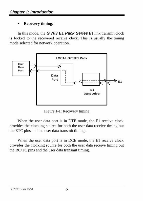
• Recovery timing:
In this mode, the G.703 E1 Pack Series E1 link transmit clock
is locked to the recovered receive clock. This is usually the timing mode selected for network operation.
Figure 1-1: Recovery timing
When the user data port is in DTE mode, the E1 receive clock provides the clocking source for both the user data receive timing out the ETC pins and the user data transmit timing.
When the user data port is in DCE mode, the E1 receive clock provides the clocking source for both the user data receive timing out the RC/TC pins and the user data transmit timing.
User Data Port
Data Port
E1
E1 transceiver
LOCAL G703E1 Pack
Chapter 1: Introduction
7 G703E1 Feb. 2000
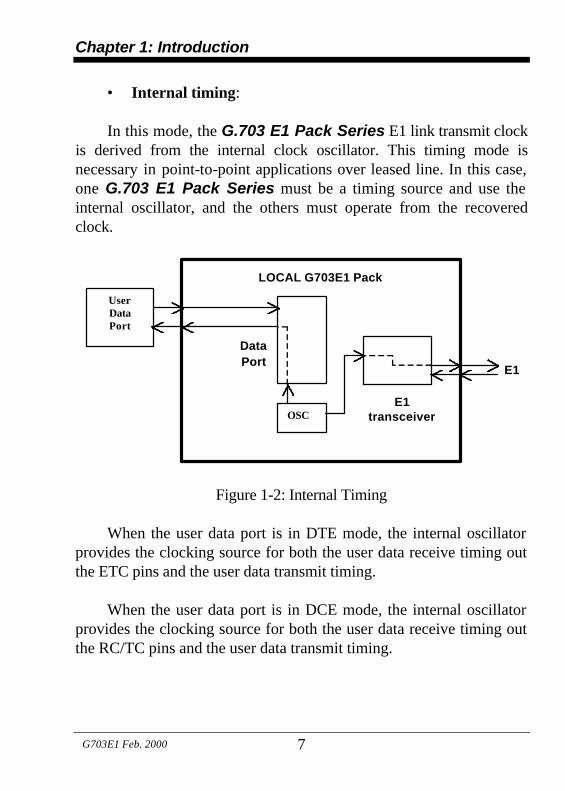
• Internal timing:
In this mode, the G.703 E1 Pack Series E1 link transmit clock
is derived from the internal clock oscillator. This timing mode is necessary in point-to-point applications over leased line. In this case, one G.703 E1 Pack Series must be a timing source and use the internal oscillator, and the others must operate from the recovered clock.
Figure 1-2: Internal Timing
When the user data port is in DTE mode, the internal oscillator provides the clocking source for both the user data receive timing out the ETC pins and the user data transmit timing.
When the user data port is in DCE mode, the internal oscillator
provides the clocking source for both the user data receive timing out the RC/TC pins and the user data transmit timing.
User Data Port
Data Port
E1
E1 transceiver
LOCAL G703E1 Pack
OSC
Chapter 1: Introduction
8 G703E1 Feb. 2000
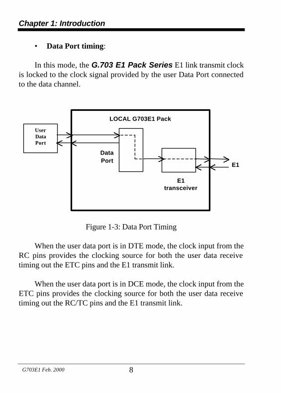
• Data Port timing:
In this mode, the G.703 E1 Pack Series E1 link transmit clock
is locked to the clock signal provided by the user Data Port connected to the data channel.
Figure 1-3: Data Port Timing
When the user data port is in DTE mode, the clock input from the RC pins provides the clocking source for both the user data receive timing out the ETC pins and the E1 transmit link.
When the user data port is in DCE mode, the clock input from the ETC pins provides the clocking source for both the user data receive timing out the RC/TC pins and the E1 transmit link.
User Data Port
Data Port
E1
E1 transceiver
LOCAL G703E1 Pack

Chapter 1: Introduction
9 G703E1 Feb. 2000
• Transparent timing:
In this mode, the G.703 E1 Pack Series E1 link receive clock
is the source for the data port receive clock while the E1 link transmit clock is locked to the clock signal provided by the user Data Port connected to the data channel.
Figure 1-4: Transparent Timing
When the user data port is in DTE mode, the E1 receive clock provides the clocking source for the user data receive timing out the ETC pins. The user data transmit timing is input from the RC pins and provides the clock for the E1 transmit link.
When the user data port is in DCE mode, the E1 receive clock provides the clocking source for the user data receive timing out the RC/TC pins. The user data transmit timing is input from the ETC pins and provides the clock for the E1 transmit link.
User Data Port
Data Port
E1
E1 transceiver
LOCAL G703E1 Pack

Chapter 1: Introduction
10 G703E1 Feb. 2000
1.3 Typical System Applications
General In a typical application (Figure 1-5), the G.703 E1 Pack Series
is used in a point-to-point connection. The synchronous data channels of each router are connected over an E1 network connection.
Figure 1-5: Point-to-Point Application using G703E1-U.
Fractional E1 data service is based on the assumption that the user data rate is a fraction of the available E1 bandwidth, in multiples of 64K.
Figure 1-6: Fractional E1 Application using G703FE1.
In the next figure, the available E1 Time Slots are divided (Fractional E1) and cascaded (multiplexed). Various data interfaces may be employed in each G.703 E1 Pack Series to provide connections between hosts, clients or PBXs across the E1 transmission facility.
Figure 1-7: Cascaded application using G703FE1-A.

Chapter 1: Introduction
11 G703E1 Feb. 2000
In the previous example, the two hosts are connected with
960Kbps bandwidth using fifteen timeslots (TS1 ~ TS15). The PBXs are also using 960Kbps on fifteen timeslots (TS17 ~ TS31).
The framing mode used above is commonly referred to as PCM30. In this framing mode, timeslot zero is used for frame alignment (FAS) and timeslot 16 is used for signaling (CAS). Of the 32 timeslots available in the E1 frame, 30 are available for carrying the data payload. The next section will describe in more detail, the framing modes for E1 transmissions.
Chapter 1: Introduction
12 G703E1 Feb. 2000
1.4 E1 signal structure
The data transferred over the E1 line is organized into frames,
with each E1 frame containing 256 bits. The 256 bits are comprised of a total of 32 time slots, each containing eight bits, that carry the data payload. The E1 line operates at a nominal rate of 2.048Mbps. If we divide that line rate by 32, the number of time slots, we find that the rate of each timeslot is 64Kbps
E1 transmission utilizes two main types of framing: Frame Alignment Signal (FAS) and Multi-Frame Alignment Signal (MFAS). Framing is necessary in order for equipment receiving the E1 signal to be able to identify and extract the individual channels. PCM-30 (CAS) transmission systems use MFAS framing along with the FAS framing. PCM-31 (CCS) transmission systems use only FAS framing. Frame Alignment Signal (FAS)
The 2.048 Mbps frame consists of 32 individual time slots (numbered 0-31). As described previously, each time slot consists of an individual 64Kbps channel of data. In the FAS format, time slot 0 of every other frame is reserved for the frame alignment signal pattern. Alternate frames contain the FAS Distant Alarm indication bit and others bits reserved for national and international use. Multi-Frame Alignment Signal (MFAS)
MFAS framing uses Channel Associated Signaling (CAS) to transmit A/B/C/D bit signaling information for each of 30 channels. This method uses the 32 time slot frame format with time slot 0 for the FAS and time slot 16 for the Multi-Frame Alignment Signal and the Channel Associated Signaling. This mode of framing is commonly used when connecting to PABX equipment.

Chapter 1: Introduction
13 G703E1 Feb. 2000
E1 line signal
The basic E1 line signal is coded using the Alternate Mark Inversion (AMI) or HDB3 rule.
In AMI coding, “ones” are alternately transmitted as positive and negative pulses, whereas “zeros” are transmitted as a zero voltage level. AMI is not used in most 2.048Mbps transmissions because synchronization loss occurs during long strings of data zeros.
In HDB3 coding, a string of four consecutive zeros is replaced with a substitute string of pulses containing an intentional bipolar violation. The HDB3 code substitutions provide high pulse density so that the receiving equipment is able to maintain synchronization with the received signal. E1 link line coding
The G703E1-U model of the G.703 E1 Pack Series supports two E1 line codes:
AMI coding. HDB3 coding.
All other models support only HDB3 coding. E1 framing formats
The G.703 E1 Pack Series supports three frame formats depending upon the model type: Models: G703E1 and G703E1-U Unframed format only! (no FAS or CAS) Models: G703FE1 and G703FE1-A Unframed format. FAS (CCS, PCM-31) format. MFAS (CAS, PCM-30) format.

Chapter 1: Introduction
14 G703E1 Feb. 2000
1.5 Technical Specifications
E1 link Framing -Unframed/Framed (G703E1 & E1-U)
-CCS (PCM31)/CAS (PCM30) -CRC4 ON/OFF
Bit Rate 2.048 Mbps Line Code -AMI (G703E1-U ONLY)
-HDB3 Line Impedance -75 ohms
-120 ohms Relative Receive Level 0 to -30dB (G703E1 &G703FE1)
0 to -43dB (G703FE1-A &G703E1-U) “Pulse” Amplitude -Nominal 2.37V±±10% for 75 ohms
-Nominal 3.00V±±10% for 120 ohms “Zero” Amplitude ±±0.1V Transmit Frequency Tracking
Internal Timing Loopback Timing External Timing
±±30 ppm ±±50 ppm ±±100 ppm
Jitter Performance According to ITU G.823 Complies With ITU G.703, G.704, G.706 and G.732 Interface Connectors -shielded RJ-45
-BNC (x2)

Chapter 1: Introduction
15 G703E1 Feb. 2000
User Data Port Channel
Interface Types -RS-530 Standard, adapter cables for
V.35, X.21, and RS-449 I/F Connectors
RS-530 Adapter Cables
V.35 I/F X.21 I/F RS-449 I/F
25 pin, D-type Female (on unit) 34 pin, M-block Female or Male available 15 pin, D-type Female or Male available 37 pin, D-type Female or Male available
Line Code NRZ Data Rate G703E1/E1-U: 2048kbps unframed only
G703FE1/FE1-A: n××64kbps where n equal 1 to 31 in CCS (PCM31) and n equal 1 to 30 in CAS (PCM30)
Clock Modes RECOVERY Receive and transmit clock (recovered) to
the synchronous Data Port INT OSC Receive and transmit clock (internal
oscillator) to the synchronous Data Port Transparent Receive clock to the synchronous, and
transmit clock from the synchronous device Data Port Receive and transmit clock from the
synchronous Data Port. Control Signals -CTS constantly ON
-DSR constantly ON, except during test loops -DCD constantly ON, except during signal loss
Time slot allocation Not Available in G703E1 or G703E1-U User defined for G703FE1 and G703FE1-A
Note for G703FE1-A: CTS is internally connected to RTS. DSR is internally connected to DTR.

Chapter 1: Introduction
16 G703E1 Feb. 2000
LED indicators (G703E1/FE1/FE1-A metal case)
DTE Green Data Port set to DTE mode DCE Green Data Port set to DCE mode Rx Sig Loss Red E1 link signal loss Tx Clk Loss Red E1 link Tx Clock loss Alarm Red E1 link alarm, include: BPV error /
CRC4 error / Frame slip / All ones(AIS) / Remote alarm
TD Yellow Transmit data (data port) RD Yellow Receive data (data port) Test Red Loopback active
LED indicators (G703E1-U plastic case)
PWR green DC applied, power switch ON Signal Loss Red E1 link signal loss Timing Loss Red E1 link Tx Clock loss TD Yellow Transmit data (data port) RD Yellow Receive data (data port) Test Red Loopback active
Physical
Metal Case type Plastic Case type Height: 30 mm 28 mm Width: 99 mm 79 mm Length: (excluding connectors) 170 mm 135 mm Weight: 360 g 180 g
Power supply
Voltage DC 9V AC Adapter for 110VAC or 220VAC
Power consumption less than 4 Watts (DC9V)
Environment
Temperature 0-60C / 32-140F Humidity 0 to 90% non-condensing

Chapter 1: Introduction
17 G703E1 Feb. 2000
Config. DIP
Switches
User Data Port DB25 Female LED Status
Indicators
Power Switch
Loopback Switch
DC Input Jack
E1 75 ohm Coaxial BNC
E1 120 ohm Twisted pair
Interface Mode LEDs
Model Sticker
G.703 Pack Series Metal Case

Chapter 1: Introduction
18 G703E1 Feb. 2000
Config. DIP Switch
User Data Port DB25 Female
LED Status Indicators
Power Switch
Loopback Switch
DC Input Jack
E1 75 ohm Coaxial BNC
E1 120 ohm Twisted pair
G.703 Pack Series Plastic Case
Chapter 2: Configuration and Operation
19 G703E1 Feb. 2000
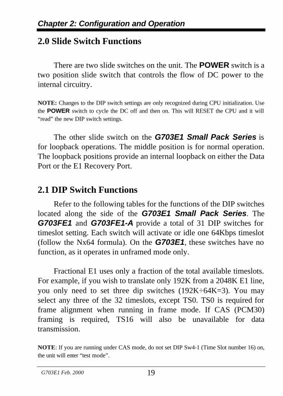
2.0 Slide Switch Functions
There are two slide switches on the unit. The POWER switch is a two position slide switch that controls the flow of DC power to the internal circuitry. NOTE: Changes to the DIP switch settings are only recognized during CPU initialization. Use the POWER switch to cycle the DC off and then on. This will RESET the CPU and it will “read” the new DIP switch settings.
The other slide switch on the G703E1 Small Pack Series is for loopback operations. The middle position is for normal operation. The loopback positions provide an internal loopback on either the Data Port or the E1 Recovery Port.
2.1 DIP Switch Functions
Refer to the following tables for the functions of the DIP switches located along the side of the G703E1 Small Pack Series. The G703FE1 and G703FE1-A provide a total of 31 DIP switches for timeslot setting. Each switch will activate or idle one 64Kbps timeslot (follow the Nx64 formula). On the G703E1, these switches have no function, as it operates in unframed mode only. Fractional E1 uses only a fraction of the total available timeslots. For example, if you wish to translate only 192K from a 2048K E1 line, you only need to set three dip switches (192K÷64K=3). You may select any three of the 32 timeslots, except TS0. TS0 is required for frame alignment when running in frame mode. If CAS (PCM30) framing is required, TS16 will also be unavailable for data transmission. NOTE: If you are running under CAS mode, do not set DIP Sw4-1 (Time Slot number 16) on, the unit will enter “test mode”.

Chapter 2: Configuration and Operation
20 G703E1 Feb. 2000
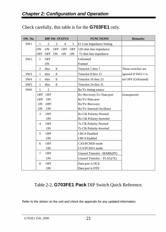
Check carefully, this table is for the G703E1 only. SW. No. DIP SW. STATUS FUNCTIONS Remarks
SW1 1 2 3 4 5 E1 Line Impedance Setting
ON ON OFF OFF OFF 120 ohm line impedance
OFF OFF ON ON ON 75 ohm line impedance
SW2 1 OFF NA (Not Applicable)
ON NA
2 thru 8 NA The G703E1
SW3 1 thru 8 NA does not support
SW4 1 thru 8 NA fractional E1 services.
SW5 1 thru 8 NA
SW6 1 2 Rx/Tx timing source
OFF OFF Rx<Recovery,Tx<Data port (transparent)
OFF
ON
ON
ON
OFF
ON
Rx/Tx<Data port
Rx/Tx<Recovery
Rx/Tx<Internal Oscillator
3 OFF Rx Clk Polarity-Normal
ON Rx Clk Polarity-Inverted
4 OFF Tx Clk Polarity-Normal
ON Tx Clk Polarity-Inverted
5 OFF NA
ON NA
6 OFF NA
ON NA
7 OFF NA
ON NA
8 OFF Data port is DCE
ON Data port is DTE
Table 2-1, G703E1 Pack DIP Switch Quick Reference. Refer to the sticker on the unit and check the appendix for any updated information.
Chapter 2: Configuration and Operation
21 G703E1 Feb. 2000
Check carefully, this table is for the G703FE1 only. SW. No. DIP SW. STATUS FUNCTIONS Remarks
SW1 1 2 3 4 5 E1 Line Impedance Setting
ON ON OFF OFF OFF 120 ohm line impedance
OFF OFF ON ON ON 75 ohm line impedance
SW2 1 OFF Unframed
ON Framed
2 thru 8 Timeslot 1 thru 7 These switches are
SW3 1 thru 8 Timeslot 8 thru 15 ignored if SW2-1 is
SW4 1 thru 8 Timeslot 16 thru 23 set OFF (Unframed)
SW5 1 thru 8 Timeslot 24 thru 31
SW6 1 2 Rx/Tx timing source
OFF OFF Rx<Recovery,Tx<Data port (transparent)
OFF
ON
ON
ON
OFF
ON
Rx/Tx<Data port
Rx/Tx<Recovery
Rx/Tx<Internal Oscillator
3 OFF Rx Clk Polarity-Normal
ON Rx Clk Polarity-Inverted
4 OFF Tx Clk Polarity-Normal
ON Tx Clk Polarity-Inverted
5 OFF CRC4 Disabled
ON CRC4 Enabled
6 OFF CAS/PCM30 mode
ON CCS/PCM31 mode
7 OFF Unused Timeslot - MARK(FF)
ON Unused Timeslot – FLAG(7E)
8 OFF Data port is DCE
ON Data port is DTE
Table 2-2, G703FE1 Pack DIP Switch Quick Reference.
Refer to the sticker on the unit and check the appendix for any updated information.

Chapter 2: Configuration and Operation
22 G703E1 Feb. 2000
Check carefully, this table is for the G703FE1-A only. SW. No. DIP SW. STATUS FUNCTIONS Remarks
SW1 1 2 3 4 5 E1 Line Impedance Setting
OFF OFF OFF OFF OFF 120 ohm line impedance Note 1
ON ON ON ON ON 75 ohm line impedance
SW2 1 OFF Unframe Note 2
ON Frame
2 thru 8 Timeslot 1 thru 7 Cascaded units MUST
SW3 1 thru 8 Timeslot 8 thru 15 NOT be assigned
SW4 1 thru 8 Timeslot 16 thru 23 identical or overlapping
SW5 1 thru 8 Timeslot 24 thru 31 timeslots.
SW6 1 2 Rx/Tx timing source
OFF OFF Rx<Recovery,Tx<Data port Cannot be used while sw6-7 ON
OFF
ON
ON
ON
OFF
ON
Rx/Tx<Data port
Rx/Tx<Recovery
Rx/Tx<Internal Oscillator
3 OFF Rx Clk Polarity-Normal
ON Rx Clk Polarity-Inverted
4 OFF Tx Clk Polarity-Normal
ON Tx Clk Polarity-Inverted
5 OFF CRC4 Disabled
ON CRC4 Enabled
6 OFF CAS/PCM30 mode
ON CCS/PCM31 mode
7 OFF Unused Timeslot - MARK(FF) When cascading, you
ON Unused Timeslot - PASS THRU MUST set this switch ON
8 OFF Data port is DCE
ON Data port is DTE
Note 1: Version prior to "0101" set termination as per G703FE1
Note 2: When set to Unframed, timeslot switches are ignored.
Table 2-3, G703FE1-A Pack DIP Switch Quick Reference.
Refer to the sticker on the unit and check the appendix for any updated information.

Chapter 2: Configuration and Operation
23 G703E1 Feb. 2000
Check carefully, this table is for the G703E1-U only. SW. No. Switch Status FUNCTIONS Remarks
1 OFF 120 ohm E1 line impedance (RJ-45 connection)
ON 75 ohm E1 line impedance (BNC connection)
2 OFF Data Port is DCE (connect to DTE)
ON Data Port is DTE (connect to DCE)
3 OFF Line Code is HDB3
ON Line Code is AMI
4 5 6 7 LBO (Line Build Out)
ON OFF ON OFF Long Haul
ON ON ON OFF Short Haul
8 9 Timing
OFF OFF Rx<Recovery, Tx<Data Port (Transparent)
ON OFF Rx/Tx<Recovery
OFF ON Rx/Tx<Data Port
ON ON Rx/Tx<Internal Oscillator
Table 2-4, G703E1-U Pack DIP Switch Quick Reference. Refer to the sticker on the unit and check the appendix for any updated information.

Chapter 2: Configuration and Operation
24 G703E1 Feb. 2000
G703E1 Pack Series DIP setting details (metal case).
DIP SW2: SETTING FRAME/UNFRAME & TIME SLOT 1-7 DIPSW NO. SW STATE FUNCTION REMARK
1 OFF UNFRAME MODE NOTE 1,3 ON FRAME MODE NOTE 2,3
2 OFF TIME SLOT 1 IDLE ON TIME SLOT 1 ACTIVE
3 OFF TIME SLOT 2 IDLE ON TIME SLOT 2 ACTIVE
4 OFF TIME SLOT 3 IDLE ON TIME SLOT 3 ACTIVE
5 OFF TIME SLOT 4 IDLE ON TIME SLOT 4 ACTIVE
6 OFF TIME SLOT 5 IDLE ON TIME SLOT 5 ACTIVE
7 OFF TIME SLOT 6 IDLE ON TIME SLOT 6 ACTIVE
8 OFF TIME SLOT 7 IDLE ON TIME SLOT 7 ACTIVE
Table 2-5, G703FE1, FE1-A Pack Setting Time Slot 1-7.
NOTE 1: In UNFRAMED MODE, the Clock Rate is FIXED at 2048KHz, therefore the settings of TIME SLOT 1-31 DIP settings do not matter. NOTE2: In FRAMED MODE, the Clock Rate = 64KxN (N = NUMBER OF TIME SLOTS active). NOTE3: In the G703E1 unit, DIP SW2-SW5 are completely ignored.
Chapter 2: Configuration and Operation
25 G703E1 Feb. 2000
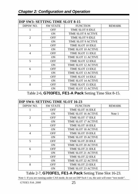
DIP SW3: SETTING TIME SLOT 8-15 DIPSW NO. SW STATE FUNCTION REMARK
1 OFF TIME SLOT 8 IDLE ON TIME SLOT 8 ACTIVE
2 OFF TIME SLOT 9 IDLE ON TIME SLOT 9 ACTIVE
3 OFF TIME SLOT 10 IDLE ON TIME SLOT 10 ACTIVE
4 OFF TIME SLOT 11 IDLE ON TIME SLOT 11 ACTIVE
5 OFF TIME SLOT 12 IDLE ON TIME SLOT 12 ACTIVE
6 OFF TIME SLOT 13 IDLE ON TIME SLOT 13 ACTIVE
7 OFF TIME SLOT 14 IDLE ON TIME SLOT 14 ACTIVE
8 OFF TIME SLOT 15 IDLE ON TIME SLOT 15 ACTIVE
Table 2-6, G703FE1, FE1-A Pack Setting Time Slot 8-15.
DIP SW4: SETTING TIME SLOT 16-23 DIPSW NO. SW STATE FUNCTION REMARK
1 OFF TIME SLOT 16 IDLE ON TIME SLOT 16 ACTIVE Note 1
2 OFF TIME SLOT 17 IDLE ON TIME SLOT 17 ACTIVE
3 OFF TIME SLOT 18 IDLE ON TIME SLOT 18 ACTIVE
4 OFF TIME SLOT 19 IDLE ON TIME SLOT 19 ACTIVE
5 OFF TIME SLOT 20 IDLE ON TIME SLOT 20 ACTIVE
6 OFF TIME SLOT 21 IDLE ON TIME SLOT 21 ACTIVE
7 OFF TIME SLOT 22 IDLE ON TIME SLOT 22 ACTIVE
8 OFF TIME SLOT 23 IDLE ON TIME SLOT 23 ACTIVE
Table 2-7, G703FE1, FE1-A Pack Setting Time Slot 16-23. Note 1: If you are running under CAS mode, do not set DIP Sw4-1 on, the unit will enter “test mode”.

Chapter 2: Configuration and Operation
26 G703E1 Feb. 2000
DIP SW5: SETTING TIME SLOT 24-31 DIPSW NO. SW STATE FUNCTION REMARK
1 OFF TIME SLOT 24 IDLE ON TIME SLOT 24 ACTIVE
2 OFF TIME SLOT 25 IDLE ON TIME SLOT 25 ACTIVE
3 OFF TIME SLOT 26 IDLE ON TIME SLOT 26 ACTIVE
4 OFF TIME SLOT 27 IDLE ON TIME SLOT 27 ACTIVE
5 OFF TIME SLOT 28 IDLE ON TIME SLOT 28 ACTIVE
6 OFF TIME SLOT 29 IDLE ON TIME SLOT 29 ACTIVE
7 OFF TIME SLOT 30 IDLE ON TIME SLOT 30 ACTIVE
8 OFF TIME SLOT 31 IDLE ON TIME SLOT 31 ACTIVE
Table 2-8, G703FE1, FE1-A Pack Setting Time Slot 24-31.
DIP SW6: FUNCTIONS DIP SW NO. SW STATE FUNCTION REMARK
1 2 OFF OFF RX timing from recovery, TX timing from data port.
Reference
OFF ON RX and TX timing all from data port. DTE/DCE timing
ON OFF RX and TX timing all from recovery.
ON ON RX and TX timing all from int. osc. Source select Table 2-11.
3 OFF RX clock polarity: NORMAL
ON RX clock polarity: INVERT
4 OFF TX clock polarity: NORMAL
ON TX clock polarity: INVERT
5 OFF CRC4 select: DISABLE NO USE ON-G703E1
ON CRC4 select: ENABLE NO USE ON-G703E1
6 OFF SIGNALING mode select: CAS NO USE ON-G703E1
ON SIGNALING mode select: CCS NO USE ON-G703E1
7 OFF IDLE code select: MARK(0xFF) NO USE ON-G703E1
ON IDLE code select: FLAG(0x7E) NO USE ON-G703E1
8 OFF DATA PORT set to DCE
ON DATA PORT set to DTE
Table 2-9, G703E1/FE1 DIP SW6 Functions.

Chapter 2: Configuration and Operation
27 G703E1 Feb. 2000
DIP SW6: FUNCTIONS DIP SW NO. SW STATE FUNCTION COMMENT
1 2 OFF OFF RX timing from recovery, TX timing from data port.
Reference
OFF ON RX and TX timing all from data port. DTE/DCE timing
ON OFF RX and TX timing all from recovery.
ON ON RX and TX timing all from int. osc. Source select Table 2-11.
3 OFF RX clock polarity: NORMAL
ON RX clock polarity: INVERT
4 OFF TX clock polarity: NORMAL
ON TX clock polarity: INVERT
5 OFF CRC4 select: DISABLE
ON CRC4 select: ENABLE
6 OFF SIGNALING mode select: CAS
ON SIGNALING mode select: CCS
7 OFF IDLE code select: MARK(0xFF) Normal
ON IDLE code select: Pass Through Cascade
8 OFF DATA PORT set to DCE
ON DATA PORT set to DTE
Table 2-10, G703FE1-A DIP SW6 Functions.
DTE/DCE TIMING SOURCE SELECT TABLE DIP SW6 SETTING
DTE MODE DCE MODE
1 2 RX TIMING TX TIMING RX TIMING TX TIMING OFF OFF Recover from E1
port Output to ETC
pins.
Source from data port.
Input from RC pins.
Recover from E1 port.
Output to RC/TC pins.
Source from data port.
Input from ETC pins.
OFF ON Source from data port.
Input from RC pins.
Output to ETC pins.
Source from data port.
Input from RC pins.
Source from data port.
Input from ETC pins.
Output to RC/TC pins.
Source from data port.
Input from ETC pins.
ON OFF Recover from E1 port
Output to ETC pins.
Source from E1 port.
Recover from E1 port.
Output to RC/TC pins.
Source from E1 port.
ON ON From internal oscillator.
Output to ETC pins.
From internal oscillator.
From internal oscillator.
Output to RC/TC pins.
From internal oscillator.
Table 2-11, G703E1 Pack Series Timing Source.
Chapter 2: Configuration and Operation
28 G703E1 Feb. 2000
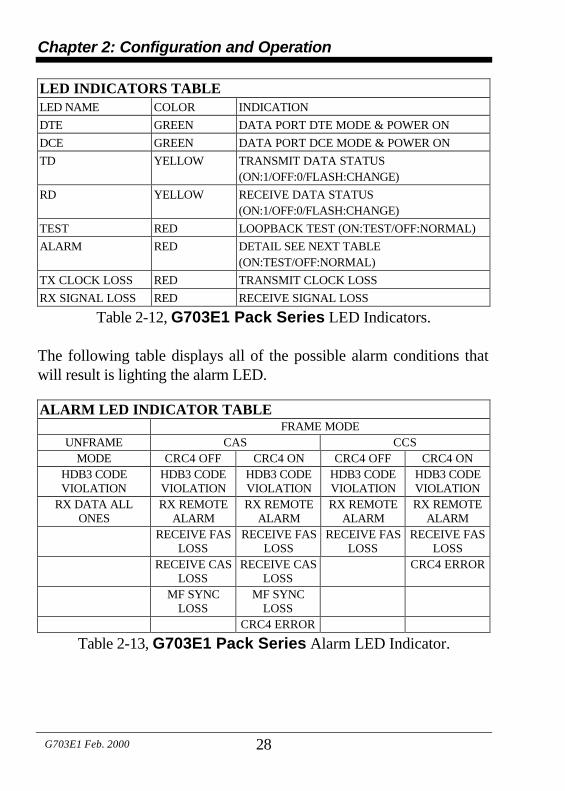
LED INDICATORS TABLE LED NAME COLOR INDICATION
DTE GREEN DATA PORT DTE MODE & POWER ON
DCE GREEN DATA PORT DCE MODE & POWER ON
TD YELLOW TRANSMIT DATA STATUS (ON:1/OFF:0/FLASH:CHANGE)
RD YELLOW RECEIVE DATA STATUS (ON:1/OFF:0/FLASH:CHANGE)
TEST RED LOOPBACK TEST (ON:TEST/OFF:NORMAL)
ALARM RED DETAIL SEE NEXT TABLE (ON:TEST/OFF:NORMAL)
TX CLOCK LOSS RED TRANSMIT CLOCK LOSS
RX SIGNAL LOSS RED RECEIVE SIGNAL LOSS
Table 2-12, G703E1 Pack Series LED Indicators. The following table displays all of the possible alarm conditions that will result is lighting the alarm LED.
ALARM LED INDICATOR TABLE FRAME MODE
UNFRAME CAS CCS MODE CRC4 OFF CRC4 ON CRC4 OFF CRC4 ON
HDB3 CODE VIOLATION
HDB3 CODE VIOLATION
HDB3 CODE VIOLATION
HDB3 CODE VIOLATION
HDB3 CODE VIOLATION
RX DATA ALL ONES
RX REMOTE ALARM
RX REMOTE ALARM
RX REMOTE ALARM
RX REMOTE ALARM
RECEIVE FAS LOSS
RECEIVE FAS LOSS
RECEIVE FAS LOSS
RECEIVE FAS LOSS
RECEIVE CAS LOSS
RECEIVE CAS LOSS
CRC4 ERROR
MF SYNC LOSS
MF SYNC LOSS
CRC4 ERROR
Table 2-13, G703E1 Pack Series Alarm LED Indicator.

Chapter 2: Configuration and Operation
29 G703E1 Feb. 2000
2.2 Examples of DIP Switch Settings
(G703FE1-A version 0101 or later) Example 1: Set line impedance to 75 ohms.
DIP SW1 1 2 3 4 5
ON ON ON ON ON Example 2a: Set line impedance to 120 ohms.
DIP SW1 1 2 3 4 5
OFF OFF OFF OFF OFF
Example 2b: Set line impedance to 120 ohms. (G703E1 / FE1)
DIP SW1 1 2 3 4 5 OFF OFF OFF
ON ON
Chapter 2: Configuration and Operation
30 G703E1 Feb. 2000
Example 3: UNFRAME mode, Clock rate fixed 2048Khz, DIPSW2-1 OFF. (G703FE1 and G703FE1-A only)
Receive timing from E1 RX recovery, Transmit timing from data port, DIP SW6-1&2 OFF.
Data port set to DCE mode, DIP SW6-8 OFF. Data port receive clock polarity: NORMAL, DIP SW6-3 OFF. Data port transmit clock polarity: NORMAL, DIP SW6-4
OFF.
NOTE: X means “Don’t Care” DIP SW2 DIP SW3
1 2 3 4 5 6 7 8 1 2 3 4 5 6 7 8
OF X X X X X X X X X X X X X X X
X X X X X X X X X X X X X X X
DIP SW4 DIP SW5 1 2 3 4 5 6 7 8 1 2 3 4 5 6 7 8
X X X X X X X X X X X X X X X X
X X X X X X X X X X X X X X X X
DIP SW6 1 2 3 4 5 6 7 8
OF OF OF OF X X X OF
X X X
Chapter 2: Configuration and Operation
31 G703E1 Feb. 2000
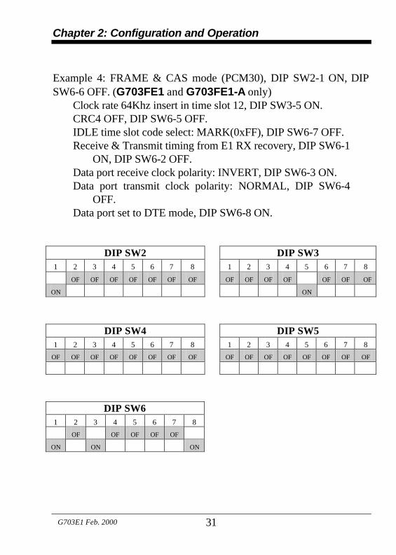
Example 4: FRAME & CAS mode (PCM30), DIP SW2-1 ON, DIP SW6-6 OFF. (G703FE1 and G703FE1-A only)
Clock rate 64Khz insert in time slot 12, DIP SW3-5 ON. CRC4 OFF, DIP SW6-5 OFF. IDLE time slot code select: MARK(0xFF), DIP SW6-7 OFF. Receive & Transmit timing from E1 RX recovery, DIP SW6-1
ON, DIP SW6-2 OFF. Data port receive clock polarity: INVERT, DIP SW6-3 ON. Data port transmit clock polarity: NORMAL, DIP SW6-4
OFF. Data port set to DTE mode, DIP SW6-8 ON.
DIP SW2 DIP SW3 1 2 3 4 5 6 7 8 1 2 3 4 5 6 7 8
OF OF OF OF OF OF OF OF OF OF OF OF OF OF
ON ON
DIP SW4 DIP SW5 1 2 3 4 5 6 7 8 1 2 3 4 5 6 7 8
OF OF OF OF OF OF OF OF OF OF OF OF OF OF OF OF
DIP SW6 1 2 3 4 5 6 7 8
OF OF OF OF OF
ON ON ON

Chapter 2: Configuration and Operation
32 G703E1 Feb. 2000
Example 5: FRAME & CCS mode (PCM31), DIP SW2-1 ON, DIP SW6-6 ON.
Clock rate 1024Khz insert in time slot 1, 2, 3, 4, 6, 8, 10, 12, 16, 18, 24, 25, 26, 27, 30, 31. (G703FE1 and G703FE1-A only)
CRC4 ON, DIP SW6-5 ON. IDLE time slot code select: FLAG(0x7E), DIP SW6-7 ON. Receive & Transmit timing from DATA PORT, DIP SW6-1
OFF, DIP SW6-2 ON. Data port receive clock polarity: NORMAL, DIP SW6-3 OFF. Data port transmit clock polarity: INVERT, DIP SW6-4 ON. Data port set to DTE mode, DIP SW6-8 ON.
DIP SW2 DIP SW3 1 2 3 4 5 6 7 8 1 2 3 4 5 6 7 8
OF OF OF OF OF OF OF
ON ON ON ON ON ON ON ON ON
DIP SW4 DIP SW5 1 2 3 4 5 6 7 8 1 2 3 4 5 6 7 8
OF OF OF OF OF OF OF OF
ON ON ON ON ON ON ON ON
DIP SW6 1 2 3 4 5 6 7 8
OF OF OF
ON ON ON ON ON
Chapter 2: Configuration and Operation
33 G703E1 Feb. 2000
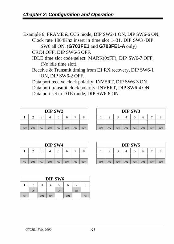
Example 6: FRAME & CCS mode, DIP SW2-1 ON, DIP SW6-6 ON.
Clock rate 1984Khz insert in time slot 1~31, DIP SW3~DIP SW6 all ON. (G703FE1 and G703FE1-A only)
CRC4 OFF, DIP SW6-5 OFF. IDLE time slot code select: MARK(0xFF), DIP SW6-7 OFF,
(No idle time slot). Receive & Transmit timing from E1 RX recovery, DIP SW6-1
ON, DIP SW6-2 OFF. Data port receive clock polarity: INVERT, DIP SW6-3 ON. Data port transmit clock polarity: INVERT, DIP SW6-4 ON. Data port set to DTE mode, DIP SW6-8 ON.
DIP SW2 DIP SW3 1 2 3 4 5 6 7 8 1 2 3 4 5 6 7 8
ON ON ON ON ON ON ON ON ON ON ON ON ON ON ON ON
DIP SW4 DIP SW5 1 2 3 4 5 6 7 8 1 2 3 4 5 6 7 8
ON ON ON ON ON ON ON ON ON ON ON ON ON ON ON ON
DIP SW6 1 2 3 4 5 6 7 8
OF OF OF
ON ON ON ON ON
Chapter 2: Configuration and Operation
34 G703E1 Feb. 2000
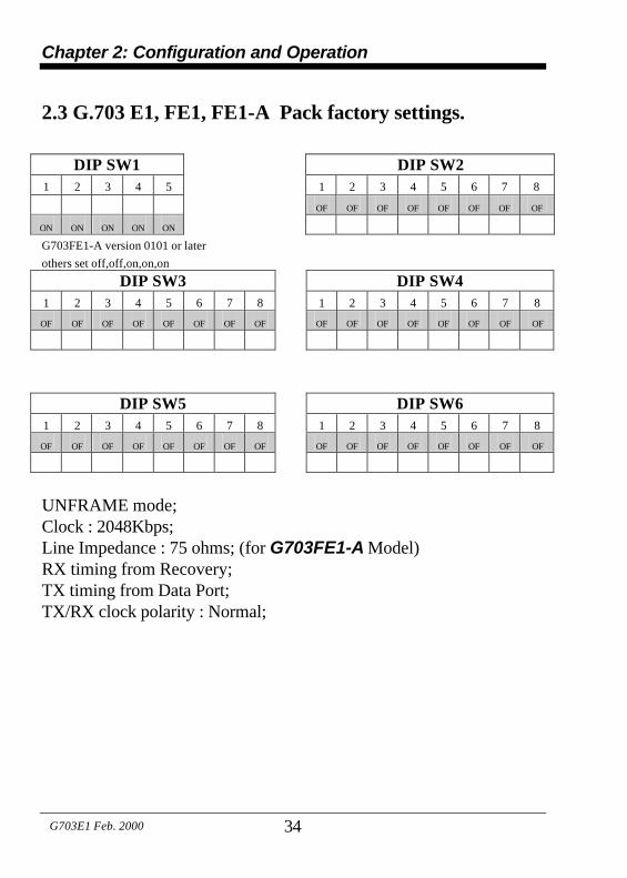
2.3 G.703 E1, FE1, FE1-A Pack factory settings.
DIP SW1 DIP SW2
1 2 3 4 5 1 2 3 4 5 6 7 8
OF OF OF OF OF OF OF OF
ON ON ON ON ON
G703FE1-A version 0101 or later
others set off,off,on,on,on
DIP SW3 DIP SW4 1 2 3 4 5 6 7 8 1 2 3 4 5 6 7 8
OF OF OF OF OF OF OF OF OF OF OF OF OF OF OF OF
DIP SW5 DIP SW6 1 2 3 4 5 6 7 8 1 2 3 4 5 6 7 8
OF OF OF OF OF OF OF OF OF OF OF OF OF OF OF OF
UNFRAME mode; Clock : 2048Kbps; Line Impedance : 75 ohms; (for G703FE1-A Model) RX timing from Recovery; TX timing from Data Port; TX/RX clock polarity : Normal;
Chapter 2: Configuration and Operation
35 G703E1 Feb. 2000
2.4 Application Notes
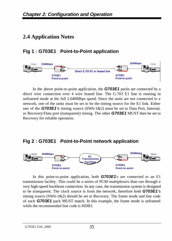
Fig 1 : G703E1 Point-to-Point application
In the above point-to-point application, the G703E1 packs are connected by a
direct wire connection over 4 wire leased line. The G.703 E1 line is running in unframed mode at the full 2.048Mbps speed. Since the units are not connected to a network, one of the units must be set to be the timing source for the E1 link. Either one of the G703E1’s timing source (SW6-1&2) must be set to Data Port, Internal, or Recovery/Data port (transparent) timing. The other G703E1 MUST then be set to Recovery for reliable operation. Fig 2 : G703E1 Point-to-Point network application
In this point-to-point application, both G703E1's are connected to an E1
transmission facility. This could be a series of PCM multiplexers than run through a very high-speed backbone connection. In any case, the transmission system is designed to be transparent. The clock source is from the network, therefore both G703E1’s timing source (SW6-1&2) should be set to Recovery. The frame mode and line code of each G703E1 pack MUST match. In this example, the frame mode is unframed while the recommended line code is HDB3.
2048kbps HostHost 2048kbps
G703E1Point-to-point
E1Transmission
Facilities
RxTx
TxRx
G703E1 Point-to-point
Chapter 2: Configuration and Operation
36 G703E1 Feb. 2000
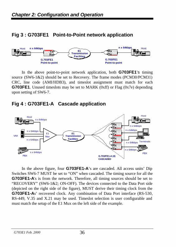
Fig 3 : G703FE1 Point-to-Point network application
In the above point-to-point network application, both G703FE1’s timing
source (SW6-1&2) should be set to Recovery. The frame modes (PCM30/PCM31) CRC, line code (AMI/HDB3), and timeslot assignment must match for each G703FE1. Unused timeslots may be set to MARK (0xff) or Flag (0x7e) depending upon setting of SW6-7. Fig 4 : G703FE1-A Cascade application
In the above figure, four G703FE1-A’s are cascaded. All access units’ Dip
Switches SW6-7 MUST be set to “ON” when cascaded. The timing source for all the G703FE1-A's is from the network. Therefore, all timing sources should be set to “RECOVERY” (SW6-1&2; ON-OFF). The devices connected to the Data Port side (depicted on the right side of the figure), MUST derive their timing clock from the G703FE1-As’ recovered clock. Any combination of Data Port interface (RS-530, RS-449, V.35 and X.21 may be used. Timeslot selection is user configurable and must match the setup of the E1 Mux on the left side of the example.
n x 64kbps HostHost n x 64kbps
G.703/FE1Point-to-point
E1Transmission
Facilities
RxTx
TxRx
G.703/FE1 Point-to-point
E1Mux
n x 64kbps
n x 64kbps
n x 64kbps
n x 64kbps
Host
Terminals
PBX
Host
VAX
PBX
n x 64kbps
n x 64kbps
n x 64kbps
n x 64kbps
G.703/FE1-A (4)CASCADED
E1Transmission
Facilities
RxTx
RxTx
RxTx
RxTx

Chapter 2: Configuration and Operation
37 G703E1 Feb. 2000
Fig 5 : G703FE1-A Cascade application
In this figure, the G703FE1-A’s are cascaded on both sides of the E1
transmission medium. The host-to-host connections are using the two timeslots 2 and 3 (SW2-3&4;ON-ON), for a combined bandwidth of 128kbps. If the cascaded pairs were directly connected, then one of the four G703FE1-A’s would have its timing source set either to the “DATA PORT” (SW6-1&2;OFF-ON) or to “Internal Oscillator” (SW6-1&2;ON-ON). The other three access units would be set to “RECOVERY” (SW6-1&2;ON-OFF). In the above network application, all units would be set to "Recovery" (SW6-1&2; ON-OFF). All access units’ Dip Switches SW6-7 MUST be set to “ON” when cascading.
Host
PBX
TS2~3 (128kbps)
G.703/FE1-A (2)CASCADED
E1Transmission
FacilitiesRxTx
RxTx
TS5~6 (128kbps)
Host
PBX
TS2~3 (128kbps)
TS5~6 (128kbps)
TxRxTxRx
G.703/FE1-A (2)CASCADED

Chapter 2: Configuration and Operation
38 G703E1 Feb. 2000
Chapter 3: Troubleshooting
39 G703E1 Feb. 2000
3.0 General
As in troubleshooting any type of computer, network, or communication problem, it is very important to follow a very logical procedure. During any troubleshooting session, the importance of taking notes cannot be overstated. It is very easy to forget connections or settings when troubleshooting a large network. Notes will help in logically checking all items and will also serve as a valuable aid in writing a system log or other report to your supervisor or your customer following successful completion of work. Notes also serve as important tools for future troubleshooting or for training of new personnel or just simply as a memory refresher.
When dealing with troubleshooting of first time installation problems, the best place to start is with double-checking of configuration settings and connections. It is very easy to misinterpret a DIP switch setting and cause the failure of a link. Initial configuration problems will also cause either immediate failure or inconsistent operations. Although the G703E1 Pack Series all comply with ITU G.703 recommendations, it is very important to understand the differences in terminology between different equipment manufactures. A thorough understanding of the settings and configuration of related equipment is mandatory when integrating many vendors' equipment.
Having the proper tools is also important in any troubleshooting endeavor. When troubleshooting E1 connections a transmission analyzer is an invaluable tool in isolating configuration, line or hardware problems. CTC Union's BTM-10 E1 Transmission Analyzer is an excellent choice. The unit is very portable, battery operated, with built-in keyboard and LCD display. The tester is designed to do BERT (Bit Error Rate) testing via E1 connection or via Data Port connection at speeds up to 2.048Mbps.

Chapter 3: Troubleshooting
40 G703E1 Feb. 2000
3.1 Connections
When checking for connection related problems, start by looking for physical defects in the connectors themselves. Check for broken or bent pins, corrosion and mis-wiring. Check cables for pinching that could indicate a broken or shorted wiring. For twisted pair wiring, confirm that a wire pair actually goes to the proper transmit or receive signal pairs. Build yourself an RJ-45 break-out-box from a pigtail converter. Loop back the pairs in the BOB and confirm continuity with a multi-meter. 3.2 Configuration
When physical connections have been confirmed, start looking for configuration problems. Confirm that the proper line code is being used. The PACK Series all support AMI and HDB3 line codes. In almost all instances, the line code will be HDB3. Confirm settings.
Framing errors can result if setting errors are made. Confirm the
mode, whether unframed, framed PCM31 or framed PCM30 and whether CRC is enabled or not. If both sides of the E1 link are using different framing, there will be alarm indications.
Data errors may result if the timeslot assignments in fractional
mode do not match. Check the settings carefully. For reduced monthly charges, a customer may only request a fraction of the E1 bandwidth. In this instance, an ISP may provide a fraction of the full 2.048Mbps bandwidth to a customer by utilizing Fractional E1. If only 512Kbps is requested, only eight (8) timeslots are required to carry the data payload. Carefully check the settings at the central site and confirm that the same eight timeslots are active on each end of the link.
Chapter 3: Troubleshooting
41 G703E1 Feb. 2000
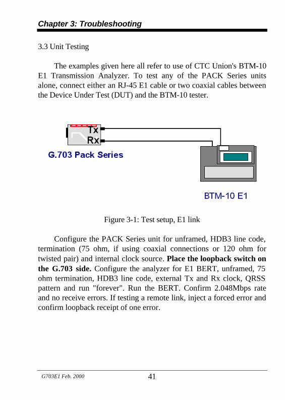
3.3 Unit Testing
The examples given here all refer to use of CTC Union's BTM-10 E1 Transmission Analyzer. To test any of the PACK Series units alone, connect either an RJ-45 E1 cable or two coaxial cables between the Device Under Test (DUT) and the BTM-10 tester.
Figure 3-1: Test setup, E1 link
Configure the PACK Series unit for unframed, HDB3 line code,
termination (75 ohm, if using coaxial connections or 120 ohm for twisted pair) and internal clock source. Place the loopback switch on the G.703 side. Configure the analyzer for E1 BERT, unframed, 75 ohm termination, HDB3 line code, external Tx and Rx clock, QRSS pattern and run "forever". Run the BERT. Confirm 2.048Mbps rate and no receive errors. If testing a remote link, inject a forced error and confirm loopback receipt of one error.

Chapter 3: Troubleshooting
42 G703E1 Feb. 2000
The BTM-10 may also be configured to do high-speed BERT
from its data port. Alternatively, our HCT-6000 or HCT-BERT 2M analyzers may be configured to connect to the data port side of the DUT. In this setup, the unit and the link may be tested.
Figure 3-2: Link testing with BTM-10 or HCT-6000
In this example, the E1 units are connected to a network and derive their timing from the network (recovery). The tester is connected directly to the RS-530 interface of the data port. The clock on the tester is set to "external". Set up for BERT test and run a pattern to the data port. Place the loopback switch of the local unit to "Data Port". The receive data will be OK if the cabling and interface are functioning properly. Remove the local data port loopback. To test the local unit and the E1 link, place the remote unit in "G.703" loopback. Now the BERT pattern should be sent to the remote unit and looped back to the local side. To test end-to-end, apply a loop at the remote host using a loopback connector.

Appendix A: Cable Definitions
43 G703E1 Feb. 2000
A.1 Pin Definitions of G703E1 Pack Series Data Port G703E1 Pack Series DB25 Data Port PIN DEFINITIONS DB25 FEMALE PIN NUMBER
PIN NAME
DTE MODE
DCE MODE
COMMENT
1 SHIELD
2 TD(A) OUTPUT INPUT
3 RD(A) INPUT OUTPUT
4 RTS(A) NOTE 1
5 CTS(A) NOTE 1
6 DSR(A) NOTE 2
7 GROUND
8 DCD(A) OUTPUT
9 RC(B) INPUT OUTPUT
10 DCD(B) OUTPUT
11 ETC(B) OUTPUT INPUT
12 TC(B) INPUT OUTPUT
13 CTS(B) NOTE 3
14 TD(B) OUTPUT INPUT
15 TC(A) INPUT OUTPUT
16 RD(B) INPUT OUTPUT
17 RC(A) INPUT OUTPUT
18 POWER IN
19 RTS(B) NOTE 3
20 DTR(A) NOTE 2
22 DSR(B) NOTE 4
23 DTR(B) NOTE 4
24 ETC(A) OUTPUT INPUT
25 GROUND NOTE 5
Table A-1, Pin Definitions of G703E1 Pack Series Data Port NOTE 1: RTS(A) AND CTS(A) INTERNALLY CONNECTED TOGETHER. NOTE 2: DSR(A) AND DTR(A) INTERNALLY CONNECTED TOGETHER. NOTE 3: RTS(B) AND CTS(B) INTERNALLY CONNECTED TOGETHER. NOTE 4: DSR(B) AND DTR(B) INTERNALLY CONNECTED TOGETHER. NOTE 5: This pin is used by the HCT-6000 and HCT-BERT/2M to determine the presence of the G703E1 Pack Series Access Unit.
G703E1 Sep. 2002

Appendix A: Cable Definitions
44 G703E1 Feb. 2000
A.2 RS-530 Cables,
25 conductor round, 1 to 1, 100cm.
Male DB25 Male(or Female) DB25 PIN PIN 1 <� � � � � � � � � � � > 1 2 <� � � � � � � � � � � > 2 3 <� � � � � � � � � � � > 3 4 <� � � � � � � � � � � > 4 5 <� � � � � � � � � � � > 5 6 <� � � � � � � � � � � > 6 7 <� � � � � � � � � � � > 7 8 <� � � � � � � � � � � > 8 9 <� � � � � � � � � � � > 9 10 <� � � � � � � � � � � > 10 11 <� � � � � � � � � � � > 11 12 <� � � � � � � � � � � > 12 13 <� � � � � � � � � � � > 13 14 <� � � � � � � � � � � > 14 15 <� � � � � � � � � � � > 15 16 <� � � � � � � � � � � > 16 17 <� � � � � � � � � � � > 17 18 <� � � � � � � � � � � > 18 19 <� � � � � � � � � � � > 19 20 <� � � � � � � � � � � > 20 21 <� � � � � � � � � � � > 21 22 <� � � � � � � � � � � > 22 23 <� � � � � � � � � � � > 23 24 <� � � � � � � � � � � > 24 25 <� � � � � � � � � � � > 25
Appendix A: Cable Definitions
45 G703E1 Feb. 2000
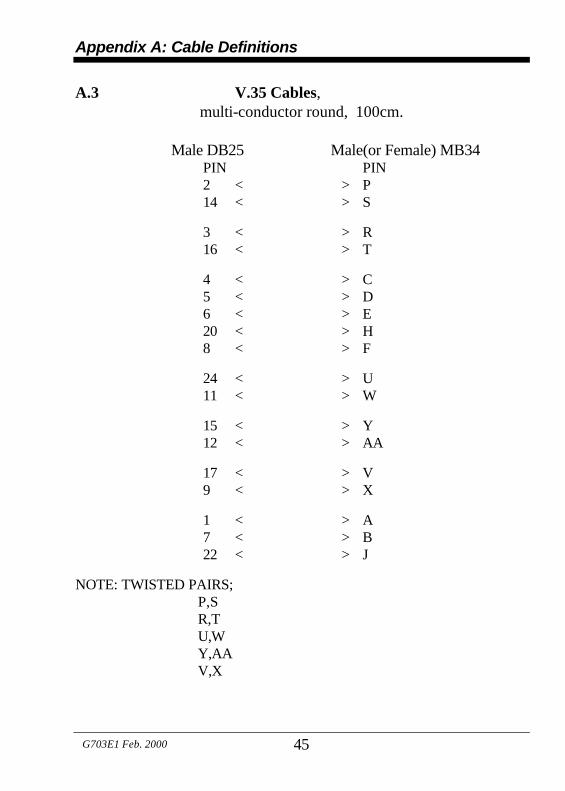
A.3 V.35 Cables,
multi-conductor round, 100cm. Male DB25 Male(or Female) MB34 PIN PIN 2 <� � � � � � � � � � � > P 14 <� � � � � � � � � � � > S
3 <� � � � � � � � � � � > R 16 <� � � � � � � � � � � > T
4 <� � � � � � � � � � � > C 5 <� � � � � � � � � � � > D 6 <� � � � � � � � � � � > E 20 <� � � � � � � � � � � > H 8 <� � � � � � � � � � � > F
24 <� � � � � � � � � � � > U 11 <� � � � � � � � � � � > W
15 <� � � � � � � � � � � > Y 12 <� � � � � � � � � � � > AA
17 <� � � � � � � � � � � > V 9 <� � � � � � � � � � � > X
1 <� � � � � � � � � � � > A 7 <� � � � � � � � � � � > B 22 <� � � � � � � � � � � > J
NOTE: TWISTED PAIRS; P,S R,T U,W Y,AA V,X
Appendix A: Cable Definitions
46 G703E1 Feb. 2000
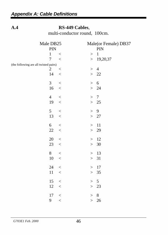
A.4 RS-449 Cables,
multi-conductor round, 100cm.
Male DB25 Male(or Female) DB37 PIN PIN 1 <� � � � � � � � � � � > 1 7 <� � � � � � � � � � � > 19,20,37 (the following are all twisted pairs)
2 <� � � � � � � � � � � > 4 14 <� � � � � � � � � � � > 22
3 <� � � � � � � � � � � > 6 16 <� � � � � � � � � � � > 24
4 <� � � � � � � � � � � > 7 19 <� � � � � � � � � � � > 25
5 <� � � � � � � � � � � > 9 13 <� � � � � � � � � � � > 27
6 <� � � � � � � � � � � > 11 22 <� � � � � � � � � � � > 29
20 <� � � � � � � � � � � > 12 23 <� � � � � � � � � � � > 30
8 <� � � � � � � � � � � > 13 10 <� � � � � � � � � � � > 31
24 <� � � � � � � � � � � > 17 11 <� � � � � � � � � � � > 35
15 <� � � � � � � � � � � > 5 12 <� � � � � � � � � � � > 23
17 <� � � � � � � � � � � > 8 9 <� � � � � � � � � � � > 26

Appendix A: Cable Definitions
47 G703E1 Feb. 2000
A.5 X.21 (DTE) Cables,
multi-conductor round, 100cm. Male DB25 Male(or Female) DB15 PIN PIN 1 <� � � � � � � � � � � > 1 7 <� � � � � � � � � � � > 8 (the following are all twisted pairs)
2 <� � � � � � � � � � � > 2 14 <� � � � � � � � � � � > 9
3 <� � � � � � � � � � � > 4 16 <� � � � � � � � � � � > 11
4 <� � � � � � � � � � � > 3 19 <� � � � � � � � � � � > 10
8 <� � � � � � � � � � � > 5 10 <� � � � � � � � � � � > 12
17 <� � � � � � � � � � � > 6 9 <� � � � � � � � � � � > 13 Note: This cable for DTE mode of Pack Series.
Appendix A: Cable Definitions
48 G703E1 Feb. 2000
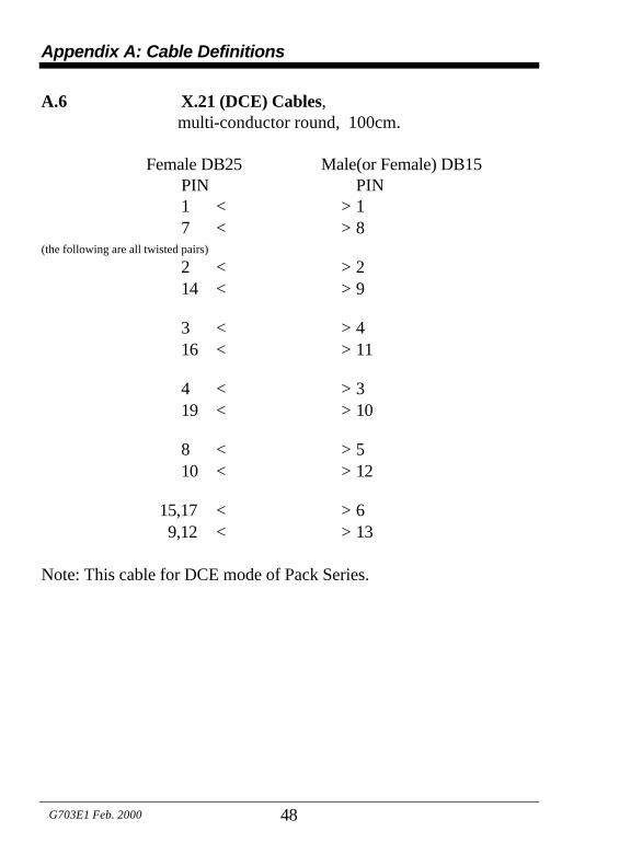
A.6 X.21 (DCE) Cables,
multi-conductor round, 100cm. Female DB25 Male(or Female) DB15 PIN PIN 1 <� � � � � � � � � � � > 1 7 <� � � � � � � � � � � > 8 (the following are all twisted pairs)
2 <� � � � � � � � � � � > 2 14 <� � � � � � � � � � � > 9
3 <� � � � � � � � � � � > 4 16 <� � � � � � � � � � � > 11
4 <� � � � � � � � � � � > 3 19 <� � � � � � � � � � � > 10
8 <� � � � � � � � � � � > 5 10 <� � � � � � � � � � � > 12
15,17 <� � � � � � � � � � � > 6 9,12 <� � � � � � � � � � � > 13 Note: This cable for DCE mode of Pack Series.
Appendix A: Cable Definitions
49 G703E1 Feb. 2000
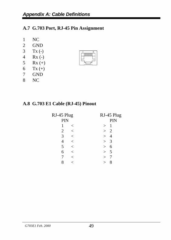
A.7 G.703 Port, RJ-45 Pin Assignment 1 NC 2 GND 3 Tx (-) 4 Rx (-) 5 Rx (+) 6 Tx (+) 7 GND 8 NC A.8 G.703 E1 Cable (RJ-45) Pinout RJ-45 Plug RJ-45 Plug PIN PIN 1 <� � � � � � � � � � � > 1 2 <� � � � � � � � � � � > 2 3 <� � � � � � � � � � � > 4 4 <� � � � � � � � � � � > 3 5 <� � � � � � � � � � � > 6 6 <� � � � � � � � � � � > 5 7 <� � � � � � � � � � � > 7 8 <� � � � � � � � � � � > 8
Appendix A: Cable Definitions
50 G703E1 Feb. 2000
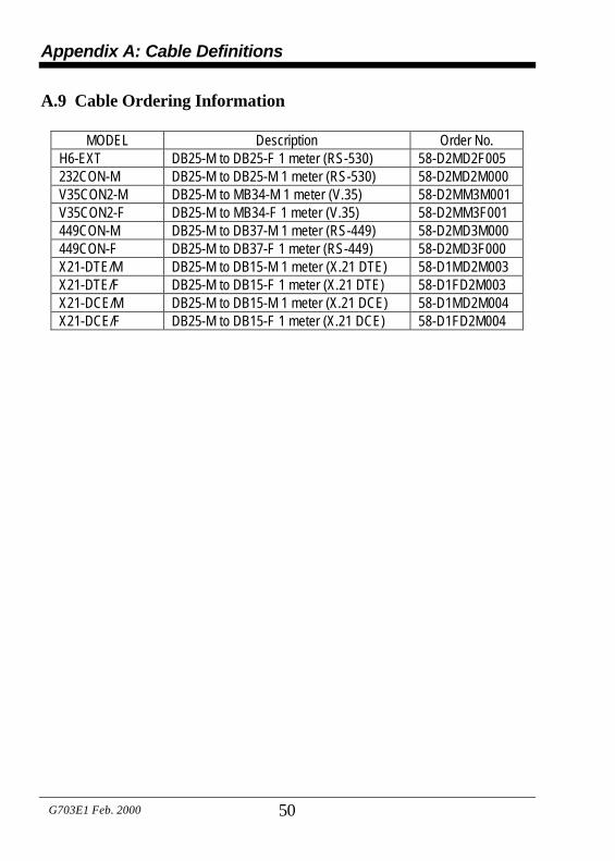
A.9 Cable Ordering Information
MODEL Description Order No. H6-EXT DB25-M to DB25-F 1 meter (RS-530) 58-D2MD2F005 232CON-M DB25-M to DB25-M 1 meter (RS-530) 58-D2MD2M000 V35CON2-M DB25-M to MB34-M 1 meter (V.35) 58-D2MM3M001 V35CON2-F DB25-M to MB34-F 1 meter (V.35) 58-D2MM3F001 449CON-M DB25-M to DB37-M 1 meter (RS-449) 58-D2MD3M000 449CON-F DB25-M to DB37-F 1 meter (RS-449) 58-D2MD3F000 X21-DTE/M DB25-M to DB15-M 1 meter (X.21 DTE) 58-D1MD2M003 X21-DTE/F DB25-M to DB15-F 1 meter (X.21 DTE) 58-D1FD2M003 X21-DCE/M DB25-M to DB15-M 1 meter (X.21 DCE) 58-D1MD2M004 X21-DCE/F DB25-M to DB15-F 1 meter (X.21 DCE) 58-D1FD2M004
51 G703E1 Feb. 2000
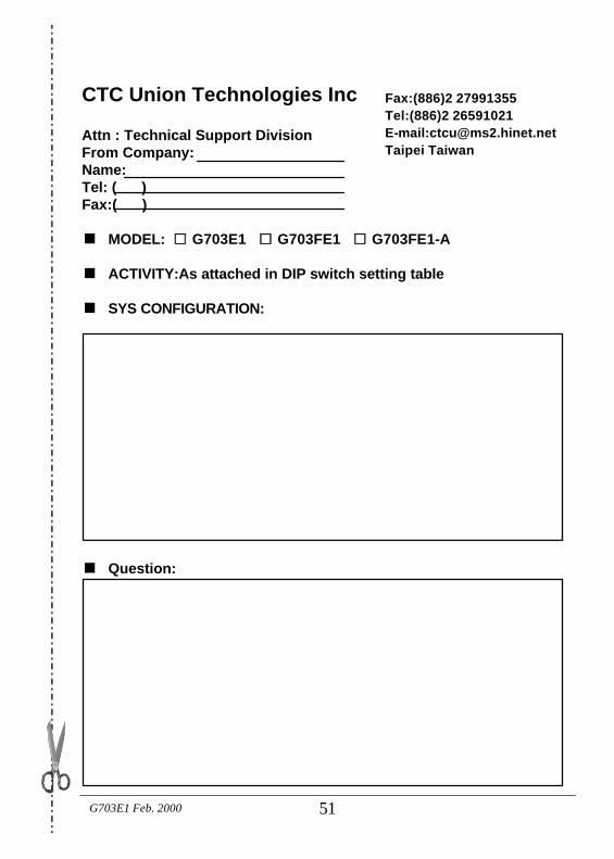
CTC Union Technologies Inc Attn : Technical Support Division From Company: Name: Tel: ( ) Fax:( )
§ MODEL: ££ G703E1 ££ G703FE1 ££ G703FE1-A
§ ACTIVITY:As attached in DIP switch setting table
§ SYS CONFIGURATION:
§ Question:
Fax:(886)2 27991355 Tel:(886)2 26591021 E-mail:[email protected] Taipei Taiwan
52 G703E1 Feb. 2000
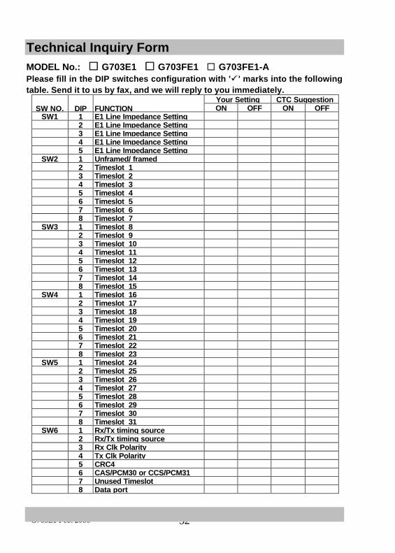
Technical Inquiry Form MODEL No.: ££ G703E1 ££ G703FE1 ££ G703FE1-A Please fill in the DIP switches configuration with 'PP ' marks into the following table. Send it to us by fax, and we will reply to you immediately.
Your Setting CTC Suggestion SW NO.
DIP
FUNCTION ON OFF ON OFF
SW1 1 E1 Line Impedance Setting 2 E1 Line Impedance Setting 3 E1 Line Impedance Setting 4 E1 Line Impedance Setting 5 E1 Line Impedance Setting
SW2 1 Unframed/ framed 2 Timeslot 1 3 Timeslot 2 4 Timeslot 3 5 Timeslot 4 6 Timeslot 5 7 Timeslot 6 8 Timeslot 7
SW3 1 Timeslot 8 2 Timeslot 9 3 Timeslot 10 4 Timeslot 11 5 Timeslot 12 6 Timeslot 13 7 Timeslot 14 8 Timeslot 15
SW4 1 Timeslot 16 2 Timeslot 17 3 Timeslot 18 4 Timeslot 19 5 Timeslot 20 6 Timeslot 21 7 Timeslot 22 8 Timeslot 23
SW5 1 Timeslot 24 2 Timeslot 25 3 Timeslot 26 4 Timeslot 27 5 Timeslot 28 6 Timeslot 29 7 Timeslot 30 8 Timeslot 31
SW6 1 Rx/Tx timing source 2 Rx/Tx timing source 3 Rx Clk Polarity 4 Tx Clk Polarity 5 CRC4 6 CAS/PCM30 or CCS/PCM31 7 Unused Timeslot 8 Data port
53 G703E1 Feb. 2000
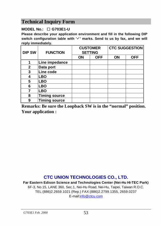
Technical Inquiry Form MODEL No.: ££ G703E1-U Please describe your application environment and fill in the following DIP switch configuration table with 'PP ' marks. Send to us by fax, and we will reply immediately.
CUSTOMER SETTING
CTC SUGGESTION DIP SW
FUNCTION
ON OFF ON OFF 1 Line impedance 2 Data port 3 Line code 4 LBO 5 LBO 6 LBO 7 LBO 8 Timing source 9 Timing source
Remarks: Be sure the Loopback SW is in the “normal” position. Your application :
CTC UNION TECHNOLOGIES CO., LTD. Far Eastern Edison Science and Technologies Center (Nei-Hu HI-TEC Park)
6F-3, No.15, LANE 360, Sec.1, Nei-Hu Road, Nei-Hu, Taipei, Taiwan R.O.C. TEL:(886)2.2659.1021 (Rep.) FAX:(886)2.2799.1355, 2659.0237
E-mail:[email protected]

54 G703E1 Feb. 2000
Commencing with the G703 Pack Series production in September 2000, the G703/FE1 and G703/FE1-A have been upgraded to version V2.0. The V2.0 units may easily be identified by their off-white color cases. The table below displays the “G703/FE1 V2.0 DIP Switch Quick Reference” table. The “G703/FE1-A V2.0 DIP Switch Quick Reference” table remains the same as the original “G703/FE1-A DIP Switch Quick Reference” table. Check carefully, this table is for the G703FE1 V2.0 only. SW. No. DIP SW. STATUS FUNCTIONS Remarks
SW1 1 2 3 4 5 E1 Line Impedance Setting OFF OFF OFF OFF OFF 120 ohm line impedance ON ON ON ON ON 75 ohm line impedance
SW2 1 OFF Unframed ON Framed 2 thru 8 Timeslot 1 thru 7 These switches are
SW3 1 thru 8 Timeslot 8 thru 15 ignored if SW2-1 is SW4 1 thru 8 Timeslot 16 thru 23 set OFF (Unframed) SW5 1 thru 8 Timeslot 24 thru 31 SW6 1 2 Rx/Tx timing source
OFF OFF Rx<Recovery,Tx<Data port (transparent) OFF
ON ON
ON OFF ON
Rx/Tx<Data port Rx/Tx<Recovery Rx/Tx<Internal Oscillator
3 OFF Rx Clk Polarity-Normal ON Rx Clk Polarity-Inverted
4 OFF Tx Clk Polarity-Normal ON Tx Clk Polarity-Inverted 5 OFF CRC4 Disabled ON CRC4 Enabled 6 OFF CAS/PCM30 mode ON CCS/PCM31 mode 7 OFF Unused Timeslot -
MARK(FF)
ON Unused Timeslot – FLAG(7E) 8 OFF Data port is DCE ON Data port is DTE
Adden. 1-1, G703FE1 V2.0 Pack DIP Switch Quick Reference.
G703E1 Sep. 2002


CTC Union Technologies Co., Ltd. Far Eastern Vienna Technology Center (Neihu HI-TEC Park) 8F, No. 60, Zhouai St., Neihu, 114, Taipei, Taiwan Phone:(886) 2.2659.1021 (Rep) Fax:(886) 2.2799.1355 E-mail: [email protected] http://www.ctcu.com