Fundamentals of DDR in QorIQ Processing...
60
External Use TM Fundamentals of DDR in QorIQ Processing Platforms FTF-NET-F0149 APR.2014 Mazyar Razzaz | Applications Engineer
-
Upload
hoangnguyet -
Category
Documents
-
view
231 -
download
1
Transcript of Fundamentals of DDR in QorIQ Processing...

External Use
TM
Fundamentals of DDR in
QorIQ Processing Platforms
FTF-NET-F0149
A P R . 2 0 1 4
Mazyar Razzaz | Applications Engineer
TM
External Use 1
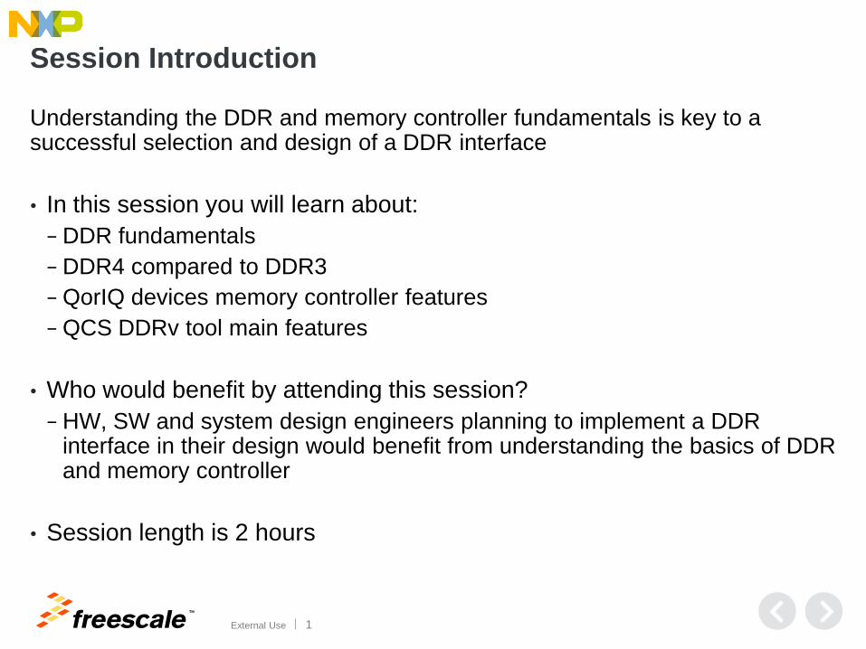
Session Introduction
Understanding the DDR and memory controller fundamentals is key to a successful selection and design of a DDR interface
• In this session you will learn about:
− DDR fundamentals
− DDR4 compared to DDR3
− QorIQ devices memory controller features
− QCS DDRv tool main features
• Who would benefit by attending this session?
− HW, SW and system design engineers planning to implement a DDR interface in their design would benefit from understanding the basics of DDR and memory controller
• Session length is 2 hours

TM
External Use 2
Learning Objectives
• By completing this training, you will be able to:
− Configure and run operate the memory controller in QorIQ devices
− Decide whether to include DDR4 or DDR3 in your board design
− Apply the DDR operational information in optimizing your SW application
− Apply the DDR4 information on your board design
− Feel more at ease with the DDR interface

TM
External Use 3
Agenda
• Industry trends
• Basic DDR SDRAM structure
• DDR3 vs. DDR4 SDRAM differences
• QorIQ DDR4 controller features
• Configurations and validation via QCS DDRv tool
TM
External Use 4
Industry Trend
• The current industry mainstream DRAM product is DDR3/3L. This
trend is expected to continue until 2015 when the pricing cross-over
is expected to occur
• Almost all Freescale networking devices offer and support
DDR3/3L
• DDR4 has been introduced and DRAM vendors are expected to
ramp production in 2014
• The first Freescale device with DDR4 support, T104x product,
taped out in Q4 2013 and has been available for sampling. All
future QorIQ products including LS1 parts will support DDR4.

TM
External Use 5
DDR3 and DDR4 – Major Vendors
• Supported by all major memory vendors

TM
External Use 6
DRAM Migration Roadmap
0%
20%
40%
60%
80%
100%
2011 2012 2013 2014 2015
DDR4
DDR3
DDR2
DDR
2011 2012 2013 2014 2015
DDR 7% 5% 2% 1% 1%
DDR2 23% 18% 13% 9% 7%
DDR3 70% 75% 75% 70% 45%
DDR4 0% 2% 10% 20% 47%
TM
External Use 7
Agenda
• Industry trends
• Basic DDR SDRAM structure
• DDR3 vs. DDR4 SDRAM differences
• QorIQ DDR4 controller features
• Configurations and validation via QCS DDRv tool
TM
External Use 8
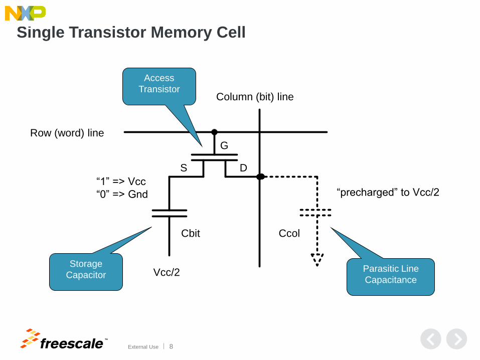
Single Transistor Memory Cell
S D
G
Cbit Ccol
Row (word) line
Column (bit) line
“1” => Vcc
“0” => Gnd
Vcc/2
“precharged” to Vcc/2
Storage
Capacitor Parasitic Line
Capacitance
Access
Transistor

TM
External Use 9
Memory Arrays
RO
W A
DD
RE
SS
DE
CO
DE
R
SENSE AMPS & WRITE DRIVERS
COLUMN ADDRESS DECODER
W0
B0
W1
W2
B1 B2 B3 B4 B5 B6 B7
TM
External Use 10
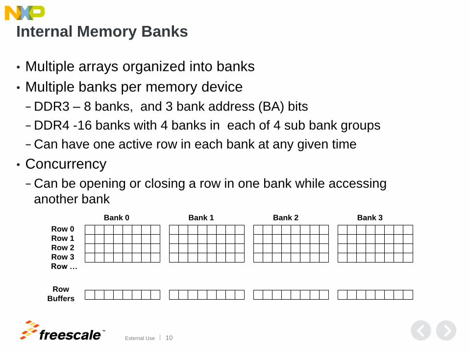
Internal Memory Banks
• Multiple arrays organized into banks
• Multiple banks per memory device
− DDR3 – 8 banks, and 3 bank address (BA) bits
− DDR4 -16 banks with 4 banks in each of 4 sub bank groups
− Can have one active row in each bank at any given time
• Concurrency
− Can be opening or closing a row in one bank while accessing
another bank
Bank 0
Row 0
Row 1
Row 3
Row 2
Bank 1 Bank 2 Bank 3
Row
Buffers
Row …

TM
External Use 11
Memory Access
• A requested row is
ACTIVATED and made
accessible through the
bank’s row buffers
• READ and/or WRITE are
issued to the active row in
the row buffers
• The row is
PRECHARGED and
is no longer accessible
through the bank’s
row buffers
Bank 0 Bank 1 Bank 2 Bank 3
Row 0
Row 1
Row 3
Row 2
Row
Buffers
Row …
Bank 0 Bank 1 Bank 2 Bank 3
Row 0
Row 1
Row 3
Row 2
Row
Buffers
Row …
Bank 0 Bank 1 Bank 2 Bank 3
Row 0
Row 1
Row 3
Row 2
Row
Buffers
Row …
TM
External Use 12
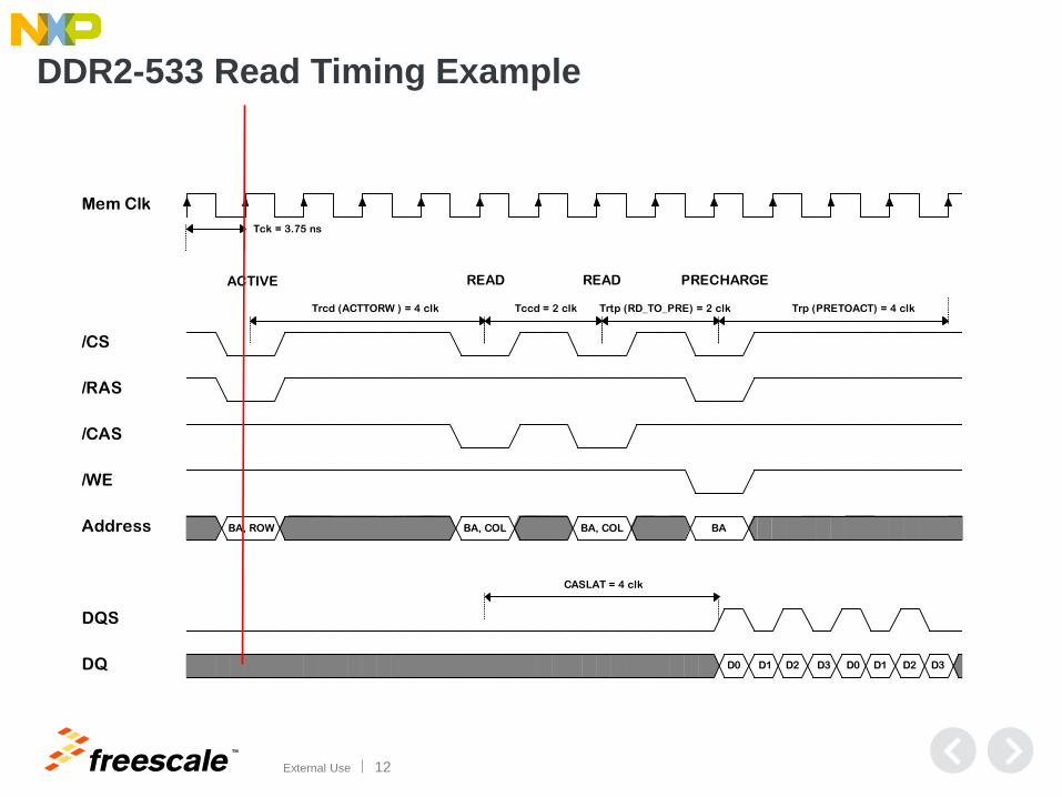
DDR2-533 Read Timing Example
Trcd (ACTTORW ) = 4 clk
Tck = 3.75 ns
Tccd = 2 clk Trtp (RD_TO_PRE) = 2 clk
BA, ROW BA, COL BA, COL BA
ACTIVE READ READ PRECHARGE
CASLAT = 4 clk
D0 D1 D2 D3 D0 D1 D2 D3
Trp (PRETOACT) = 4 clk
Mem Clk
/CS
/RAS
/CAS
/WE
Address
DQS
DQ

TM
External Use 13
Memory Interconnects
(Ideal Condition)
Controller
Differential
Strobe
Data
Data Write Cycle
TM
External Use 14
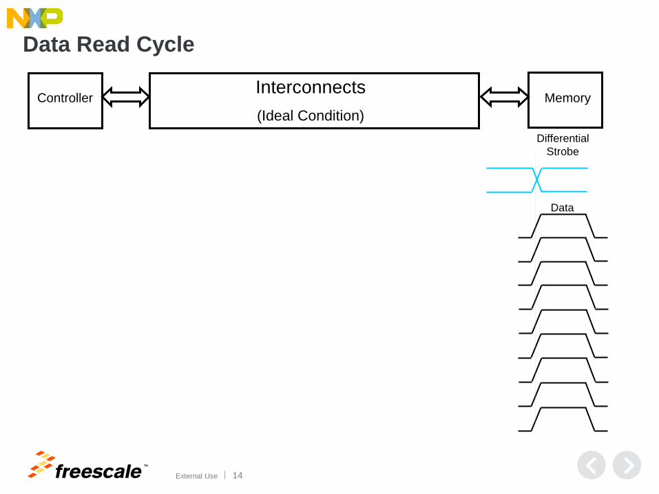
Controller Interconnects
(Ideal Condition)
Memory
Differential
Strobe
Data
Data Read Cycle

TM
External Use 15
Example – DDR2/3/4 SDRAM
• Micron MT47H32M8
• 32M x 8 (8M x 8 x 4 banks)
• 256 MB total
• 13-bit row address
− 8K rows
• 10-bit column address
− 1K bits/row (1KB in x8 data with DRAM)
• 2-bit bank address
• Data bus: DQ, DQS, /DQS, DM
• ADD bus: A, BA, /CS, /RAS, /CAS,
/WE, ODT, CKE, CK, /CK
32M x 8
256 Mb13
2
8ADDR
BANK ADDR
DATA
DATA
STROBE(S)
DATA
MASK
ODT
/CS
/RAS
/CAS
/WE
CKE
CK
/CK
A[12:0]
BA[1:0]
Command
Bus
CK
DQ[7:0]
DQS
/DQS
DM
ODT
DATA bus
ADD bus

TM
External Use 16
Example – DDR2/3/4 DIMM
• Micron MT9HTF3272A
• 9 each 32M x 8 memory devices
• 32M x 72 overall
• 256 MB total, single “rank”
• 9 “byte lanes”
Two Signal Bus
• 1- Address, command, control, and
clock signals are shared among all 9
DRAM devices
• 2- Data, strobe, data mask not shared
32M x 8
/CS
/RAS
/CAS
/WE
CKE
CK
/CK
A[12:0]
BA[1:0]
DQ[7:0]
DQS
/DQS
DM
ODT
32M x 8
/CS
/RAS
/CAS
/WE
CKE
CK
/CK
A[12:0]
BA[1:0]
DQ[7:0]
DQS
/DQS
ODT
MDQ[0:7], MDQS0, MDM0
MDQ[48:55], MDQS6, MDM6
MDQ[8:15], MDQS1, MDM1
MDQ[16:23], MDQS2, MDM2
MDQ[24:31 MDQS3, MDM3
MDQ[32:39], MDQS4, MDM4
MDQ[40:47], MDQS5, MDM5
MDQ[56:31], MDQS7, MDM7
ECC[0:7], MDQS8, MDM8
/CSn ODTn
DM
TM
External Use 17
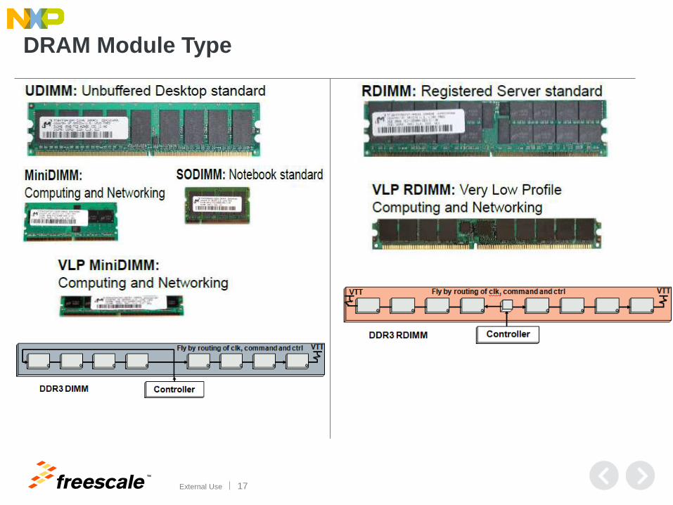
DRAM Module Type

TM
External Use 18
Agenda
• Industry trends
• Basic DDR SDRAM structure
• DDR3 vs. DDR4 SDRAM differences
• QorIQ DDR4 controller features
• Configurations and validation via QCS DDRv tool

TM
External Use 19
DDR SDRAM Highlights and Comparison
Feature/Category DDR3 DDR4
Package BGA only BGA only
Densities 512Mb -8Gb 2Gb -16Gb
Voltage DDR3L:1.35V Core & I/O
DDR3: 1.5V Core & I/O
1.2V Core
1.2V I/O, also 2.5V external VPP
Data I/O
CMD, ADDR I/O
Center Tab Termination (CTT)
CTT
Pseudo Open Drain (POD)
CTT
Internal Memory Banks 8 16 for x4/x8
8 for x16
Data Rate 800 DDR3/3L:2133/1866 Mbps 1600–3200 Mbps
VREF VREFCA & VREFDQ external VREFCA external
VREFDQ internal
Data Strobes/Prefetch/Burst
Length/Burst Type
Differential/8-bits/BC4, BL8/ Fixed,
OTF
Same as DDR3
Additive/read/write Latency 0, CL-1, CL-2/ AL+CL/ AL +CWL Same as DDR3

TM
External Use 20
DDR SDRAM Highlights and Comparison (continued)
Feature/Category DDR3 DDR4
CRC Data Bus No Yes
Boundary Scan/Connectivity
test (TEN pin) No Yes
Bank Grouping No Yes
Data Bus Inversion
(DBI_n pin) No Yes
Write Leveling / ZQ Yes Yes
ACT_n new pin & command No Yes
Low power auto self-refresh No Yes

TM
External Use 21
DDR3/DDR3L/DDR4 Power Saving
• DDR3 DRAM provides 20%
power savings over DDR2
• DDR3L DRAM provides 10%
power saving over DDR3
• DDR4 DRAM provides 37%
power saving over DDR3L
TM
External Use 22
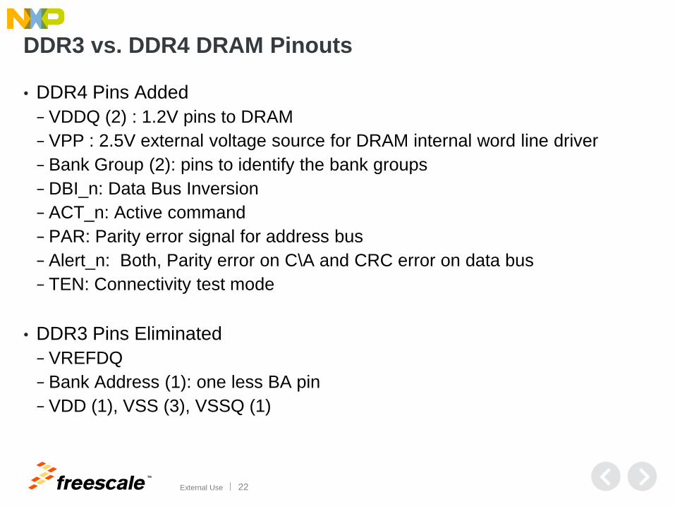
DDR3 vs. DDR4 DRAM Pinouts
• DDR4 Pins Added
− VDDQ (2) : 1.2V pins to DRAM
− VPP : 2.5V external voltage source for DRAM internal word line driver
− Bank Group (2): pins to identify the bank groups
− DBI_n: Data Bus Inversion
− ACT_n: Active command
− PAR: Parity error signal for address bus
− Alert_n: Both, Parity error on C\A and CRC error on data bus
− TEN: Connectivity test mode
• DDR3 Pins Eliminated
− VREFDQ
− Bank Address (1): one less BA pin
− VDD (1), VSS (3), VSSQ (1)

TM
External Use 23
DRAM Densities DDR3 VS. DDR4
• 16 Banks for x4 and x8 DRAM DDR4, 8 Banks for x16
• 4Gb is DRAM’s vendors choice for starting DDR4 density.
• Larger memory size is one reasons to use x4 vs. x8 vs. x16 DRAM
• Data mask or Data bus inversion (DBI), not available in x4 DRAM
Density 1Gb 2Gb 4Gb 8Gb 16 Gb Width x4 x8 x16 x4 x8 x16 x4 x8 x16 x4 x8 x16 x4 x8 x16
DD
R3
Banks 8 8 8 8 8 8 8 8 8 8 8 8
Rows 14 14 13 15 15 14 16 16 15 16 16 16
Columns 11 10 10 11 10 10 11 10 10 12 11 11
Row Size (KB) 1 1 2 1 1 2 1 1 2 2 2 2
DD
R4
Banks 16 16 8 16 16 8 16 16 8 16 16 8
Rows 15 14 14 16 15 15 17 16 16 18 17 17
Columns 10 10 10 10 10 10 10 10 10 10 10 10
Row Size (KB) 0.5 1 2 0.5 1 2 0.5 1 2 0.5 1 2

TM
External Use 24
Modules DDR3 vs. DDR4
• U/RDIMM Pin count of 240 vs. 288, Pin pitch of 1.0mm vs. 0.85mm
• Bottom edge step ramp vs. flat. Height & width increased by ~1mm
• DRAM ball count and ball pitch not changed
• DIMM topology of fly-by for address/command bus not changed
• SoDIMM Pin count of 204 vs. 260
• SoDIMM will have native ECC support vs. non compatible pinout in
DDR3

TM
External Use 25
Agenda
• Industry trends
• Basic DDR SDRAM structure
• DDR3 vs. DDR4 SDRAM differences
• QorIQ DDR4 controller features
• Configurations and validation via QCS DDRv tool

TM
External Use 26
Common DDR3 and DDR4 Controller Features
• Supports most JEDEC standard x8, x16 DDR3L & DDR4 devices
• Memory device densities from 1Gb – through 8Gb
• Data rates up to: 1600 MT/s DDR3L and DDR4
• Devices with 12-16 row address bits, 8-11 column address bits, 2-3 logical bank address bits
• Data mask signals for sub-double word writes
• Up to four physical banks (ranks / chip selects)
• Physical bank (rank) sizes up to 8GB/16GB for DDR3L/DDR4
• Physical bank interleaving between 2 or 4 chip selects
• Memory controller interleaving when more than 1 controller is available
• Un-buffered or registered DIMMs

TM
External Use 27
Common DDR3 and DDR4 Controller Features (continued)
• Up to 32 / 64 open pages for DDR3L / DDR4
− Amount of time rows stay open is programmable
• Auto pre-charge, globally or by chip select
• Self refresh
• Up to 8 posted refreshes
• Automatic or software-controlled memory device initialization
• ECC: 1-bit error correction, 2-bit error detection, detection of all errors within a nibble
• ECC error injection
• Read-modify-write for sub-double word writes when using ECC
• Automatic data initialization for ECC
• Dynamic power management
TM
External Use 28
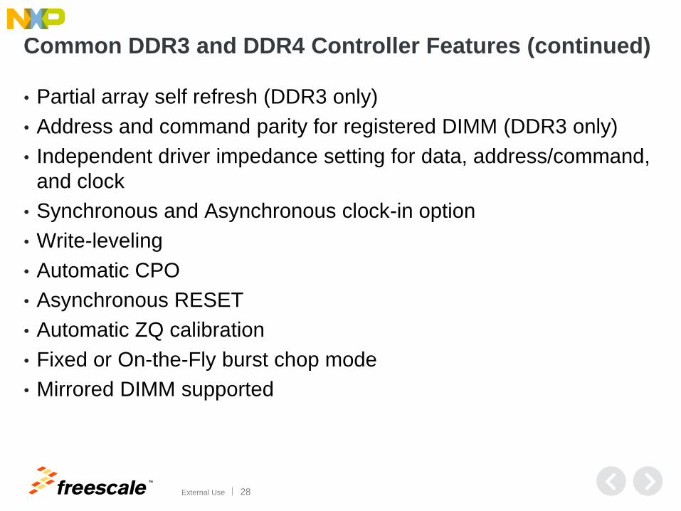
Common DDR3 and DDR4 Controller Features (continued)
• Partial array self refresh (DDR3 only)
• Address and command parity for registered DIMM (DDR3 only)
• Independent driver impedance setting for data, address/command,
and clock
• Synchronous and Asynchronous clock-in option
• Write-leveling
• Automatic CPO
• Asynchronous RESET
• Automatic ZQ calibration
• Fixed or On-the-Fly burst chop mode
• Mirrored DIMM supported

TM
External Use 29
DDR4-only Controller Features
• Internal DQa Vref supply and calibration, both controller and DRAM
• Data write CRC
• Data inversion bus
• Address bus parity error
• 16 banks for higher concurrency
• Connectivity test mode
• ODT park and buffer disable
• DRAM mode register readout capability
• Low power auto self refresh
• Temp controlled auto refresh
• Pseudo open drain (POD) driver and termination
• Command Address latency (CAL)

TM
External Use 30
Fly By Routing Topology
• Introduction of “Fly-by” architecture
− Address, command, control & clocks
− Improved signal integrity…enabling higher speeds
− On module termination
Controller
VTT Fly by routing of clk, command and ctrl
Controller
Matched tree routing of clk command and ctrl
DDR2 DIMM
DDR3 & DDR4 DIMM

TM
External Use 31
Write Adjustment
Freescale
Chip
Address,
Command
& Clock Bus
Data Lanes
Write leveling sequence during the initialization process will determine the
appropriate delays to each strobe/data byte lane and add this delay for every write
cycle.
• Write leveling used to add delay
to each strobe/data line.
TM
External Use 32
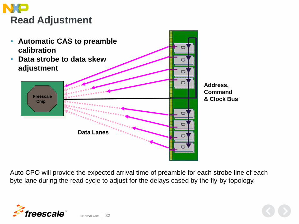
Read Adjustment
Freescale
Chip
Address,
Command
& Clock Bus
Data Lanes
Auto CPO will provide the expected arrival time of preamble for each strobe line of each
byte lane during the read cycle to adjust for the delays cased by the fly-by topology.
• Automatic CAS to preamble
calibration
• Data strobe to data skew
adjustment
TM
External Use 33
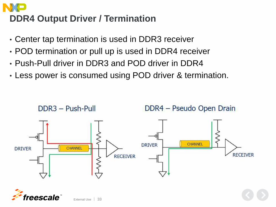
DDR4 Output Driver / Termination
• Center tap termination is used in DDR3 receiver
• POD termination or pull up is used in DDR4 receiver
• Push-Pull driver in DDR3 and POD driver in DDR4
• Less power is consumed using POD driver & termination.
TM
External Use 34
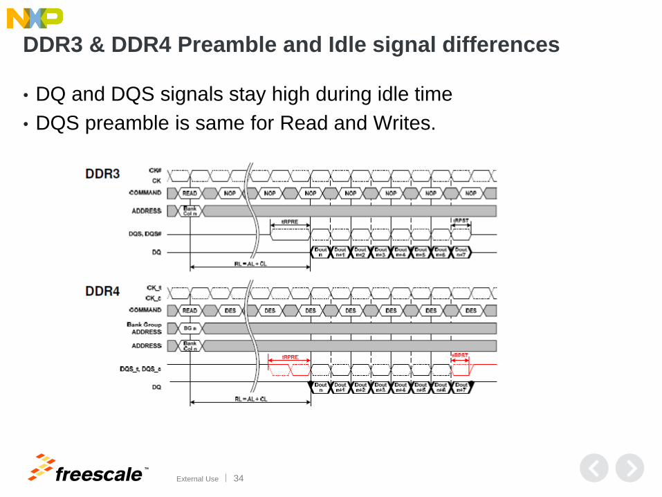
DDR3 & DDR4 Preamble and Idle signal differences
• DQ and DQS signals stay high during idle time
• DQS preamble is same for Read and Writes.
TM
External Use 35
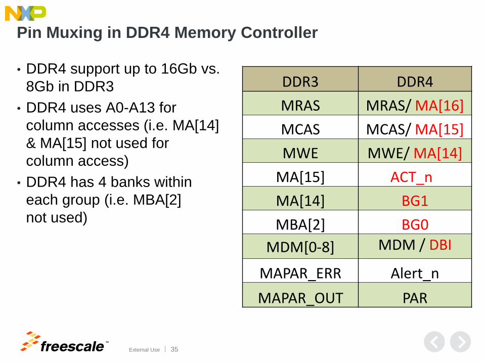
Pin Muxing in DDR4 Memory Controller
• DDR4 support up to 16Gb vs.
8Gb in DDR3
• DDR4 uses A0-A13 for
column accesses (i.e. MA[14]
& MA[15] not used for
column access)
• DDR4 has 4 banks within
each group (i.e. MBA[2]
not used)
DDR3 DDR4
MRAS MRAS/ MA[16]
MCAS MCAS/ MA[15]
MWE MWE/ MA[14]
MA[15] ACT_n
MA[14] BG1
MBA[2] BG0
MDM[0-8] MDM / DBI
MAPAR_ERR Alert_n
MAPAR_OUT PAR

TM
External Use 36
New pin: ACT_n
• ACT_n is a single pin for Active command input
• When ACT_n is low:
− ACT Command is asserted
− WE/CAS/RAS pins will be treated as address pins (A14:A16)
• When ACT_n is high
− WE/CAS/RAS pins will be treated as command pins

TM
External Use 37
New pin: DBI_n
• Active low input/output for data bus inversion mode
• As an input to DRAM, a low on DBI_n indicates that the DRAM
inverts write data received on the DQ inputs
• As an output from the DRAM, a low on DBI_n indicates that the
DRAM has inverted the data on its DQ outputs.
• Maximum of half of the bits driven low including DBI_n pin
• Available only on x8 and x 16 DRAM
• PROs: Fewer bits driven low means less noise, better data eye and
lower power consumption
• CONs: Data mask is not available, performance is affected with
read-modify-writes when writes are not multiples of 8 bytes or not
aligned to 0 or 8 address. CAS_LAT is increased by 2 clocks.

TM
External Use 38
Data Bus Inversion - DBI
• If more than 4 bits of a byte lane are low, invert the data and drive
the DBI_n pin low
• If 4 or less bits of a byte lane are low, do not invert the data and
drive the DBI_n pin high
Controller Data Bus Memory
DQ0 0 1 0 0 1 1 0 1 0 1 0 0
DQ1 1 1 0 0 0 1 0 1 1 1 0 0
DQ2 0 0 0 0 1 0 0 1 0 0 0 0
DQ3 0 1 1 0 1 1 1 1 0 1 1 0
DQ4 0 1 0 0 1 1 0 1 0 1 0 0
DQ5 1 0 1 0 0 0 1 1 1 0 1 0
DQ6 1 1 1 0 0 1 1 1 1 1 1 0
DQ7 0 0 1 0 1 0 1 1 0 0 1 0
DBI_n 0 1 1 0
# low bits 5 3 4 8 4 3 4 1
TM
External Use 39
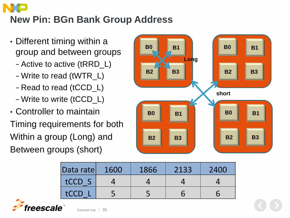
New Pin: BGn Bank Group Address
• Different timing within a
group and between groups
− Active to active (tRRD_L)
− Write to read (tWTR_L)
− Read to read (tCCD_L)
− Write to write (tCCD_L)
• Controller to maintain
Timing requirements for both
Within a group (Long) and
Between groups (short)
B0 B1
B2 B3
B0 B1
B2 B3
B0 B1
B2 B3
B0 B1
B2 B3
short
Long
Data rate 1600 1866 2133 2400
tCCD_S 4 4 4 4
tCCD_L 5 5 6 6
TM
External Use 40
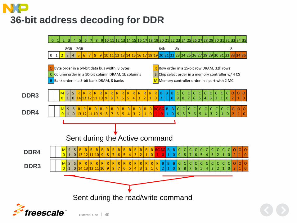
36-bit address decoding for DDR
0 1 2 3 4 5 6 7 8 9 10 11 12 13 14 15 16 17 18 19 20 21 22 23 24 25 26 27 28 29 30 31 32 33 34 35
Sent during the Active command
Sent during the read/write command
8GB 2GB 64k 8k 8
0 1 2 3 4 5 6 7 8 9 10 11 12 13 14 15 16 17 18 19 20 21 22 23 24 25 26 27 28 29 30 31 32 33 34 35
O Byte order in a 64-bit data bus width, 8 bytes R Row order in a 15-bit row DRAM, 32k rows
C Column order in a 10-bit column DRAM, 1k columns S Chip select order in a memory controller w/ 4 CS
B Bank order in a 3-bit bank DRAM, 8 banks M Memory controller order in a part with 2 MC
M 0
S 1
S 0
R 14
R 13
R 12
R 11
R 10
R 9
R 8
R 7
R 6
R 5
R 4
R 3
R 2
R 1
R 0
B 2
B 1
B 0
C 9
C 8
C 7
C 6
C 5
C 4
C 3
C 2
C 1
C 0
O 2
O 1
O 0
M 0
S 1
S 0
R 14
R 13
R 12
R 11
R 10
R 9
R 8
R 7
R 6
R 5
R 4
R 3
R 2
R 1
R 0
B 2
B 1
B 0
C 9
C 8
C 7
C 6
C 5
C 4
C 3
C 2
C 1
C 0
O 2
O 1
O 0
M 0
S 1
S 0
R 13
R 12
R 11
R 10
R 9
R 8
R 7
R 6
R 5
R 4
R 3
R 2
R 1
R 0
BG 1
BG 0
B 1
B 0
C 9
C 8
C 7
C 6
C 5
C 4
C 3
C 2
C 1
C 0
O 2
O 1
O 0
M 0
S 1
S 0
R 13
R 12
R 11
R 10
R 9
R 8
R 7
R 6
R 5
R 4
R 3
R 2
R 1
R 0
BG 1
BG 0
B 1
B 0
C 9
C 8
C 7
C 6
C 5
C 4
C 3
C 2
C 1
C 0
O 2
O 1
O 0
DDR4
DDR4
DDR3
DDR3
TM
External Use 41
New Pin: Parity
• C/A Parity signal (PAR) covers ACT_n, RAS_n, CAS_n, WE_n and
the address bus. Control signals CKE, ODT, CS_n are not included
• Even parity, i.e. valid parity is defined as an even number of ones
across the inputs used for parity computation combined with the
parity signal. The parity bit is chosen so that the total number of ‘1’s
in the transmitted signal, including the parity bit is even
• Commands must be qualified by CS_n
• Alert_n used to flag error to memory controller
• PROs: Better reliability
• CONs: PL (4clk for 2133, 5clk for 2400) is added to read latency

TM
External Use 42
New Pin Alert_n & Cyclic Redundancy Check (CRC)
• Alert_n – Active low output signal that indicates an error event for
both the C/A Parity Mode and the CRC Data Mode
• CRC Data mode:
− To detect data errors during write cycles .
− Polynomial encoding is used to generate the CRC for every 8-bit
− Two beats added to the write burst to transfer the CRC header
− DRAM generates a CRC checksum per each write burst and DQS lane
− DRM compares the generated checksum to controllers checksum
− If Data Mask is disabled, corrupt data is written, with the Alert_n flag sent
to controller to retry the write.
− If Data Mask is enabled, corrupt data is not written, with the Alert_n flag
sent to controller to retry the write.

TM
External Use 43
Low Power Auto Self Refresh
• While DRAM is in self-refresh mode, four refresh mode options
available:
− Manual mode, normal temperature (45C – 85C)
− Manual mode, extended temperature (85C – 95C)
− Manual mode, reduced temperature (0C – 45C)
− Automatic mode: automatically switches between modes based on
temperature sensor measurements
• Power savings by reducing refresh rate when possible
Auto Self Refresh DDR4 DDR3
Extended Range 85˚C-95˚C 85˚C-95˚C
Normal Range 45˚C-85˚C 0˚C-85˚C
Reduced Range 0˚C-45˚C
TM
External Use 44
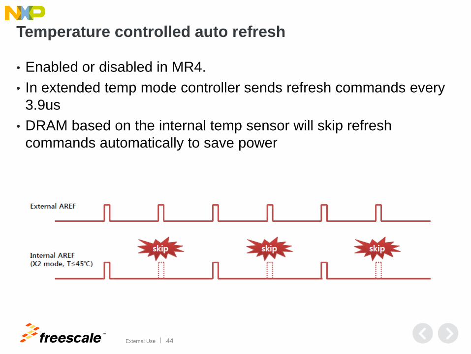
Temperature controlled auto refresh
• Enabled or disabled in MR4.
• In extended temp mode controller sends refresh commands every
3.9us
• DRAM based on the internal temp sensor will skip refresh
commands automatically to save power

TM
External Use 45
ADDR/CMD RCVR
Is switched OFF
Command Address Latency (CAL)
• DDR4 supports CAL as a power savings feature.
• In default mode, DRAM C/A input receivers are always on
• In CAL mode, only CS receiver is always on. all remaining
C/A input receivers are kept in a low power state while not in
use. CS signal is sent N number of cycles earlier to allow
DRAM time to wake up C/A input receivers.

TM
External Use 46
DRAM Receiver Data Eye Mask and BER
• Bit error rate (BER) – similar to SerDes – is defined for DRAM
receiver measurement
• DRAM receiver data mask is defined for random and deterministic
Jitter as data rates approaching 3GT/s
• For LS1, and T1 (i.e. data rates of 1600MT/s or less) we will
continue with the conventional setup and hold time measurements

TM
External Use 47
Agenda
• Industry trends
• Basic DDR SDRAM structure
• DDR3L vs. DDR4 SDRAM differences
• QorIQ DDR4 controller features
• Configurations and validation via QCS DDRv tool

TM
External Use 48
DDR3 and DDR4 Initialization Flow
Power-up
DDR
Reset
DDR
CTRL
INIT
Chip selects
enabled and
DDR clocks
begin
Asserted at
least 200us
Stable
CLKS CKE = HIGH
DRAMs
Initialized Mode Register
Commands Issued
ZQ
Calibration
Write
Leveling
Read
Adjust
Controller
Started
MEM_EN =1
Automatic CAS-to-Preamble
(aka Read Leveling)….
Plus Data-to-Strobe adjustment
ZQCL Issued (512 clocks)
Also DLL lock time is
occurring
Init
Complete Ready for User
accesses
Automatically handled
By the controller
Need at
least 500us
from reset
de-assertion
to the
controller
being
enabled.
Timed loop
may be
needed.
Write
Adjust Data-to-Strobe adjustment for write
cycles. Only DDR4: DRAM Data
bus VREF calibration
TM
External Use 49
Register configuration
Two general type of registers to be configured in the memory controller
• First register type are set to the DRAM related parameter values, that are provided via SPD or DRAM datasheet. Over 100 register fields fall under this category.
• Second register type are the Non-SPD values that are set based on customer’s application. For example:
− On-die-termination (ODT) settings for DRAM and controller
− driver impedance setting for DRAM and controller
− Clock adjust value selection
− Write-leveling start value (WRLVL_START)
TM
External Use 50
Using QCS DDRv Tool
• Configure, and optimize your DDR interface in matter of hours.
1. Use the tool to generate the DDR register settings • Use the latest revision
• Select the SPD option in configuration wizard when DIMM is used
• Select Auto Configuration when Discrete DRAM is used
2. Optimize the DDR register setting on your QorIQ board • Run the clock centering test
• Optimize the ODT and drive strength for read and write
• DDRv DEMO: http://www.freescale.com/webapp/sps/site/prod_summary.jsp?code=PE_QORIQ_DDRV
TM
External Use 51
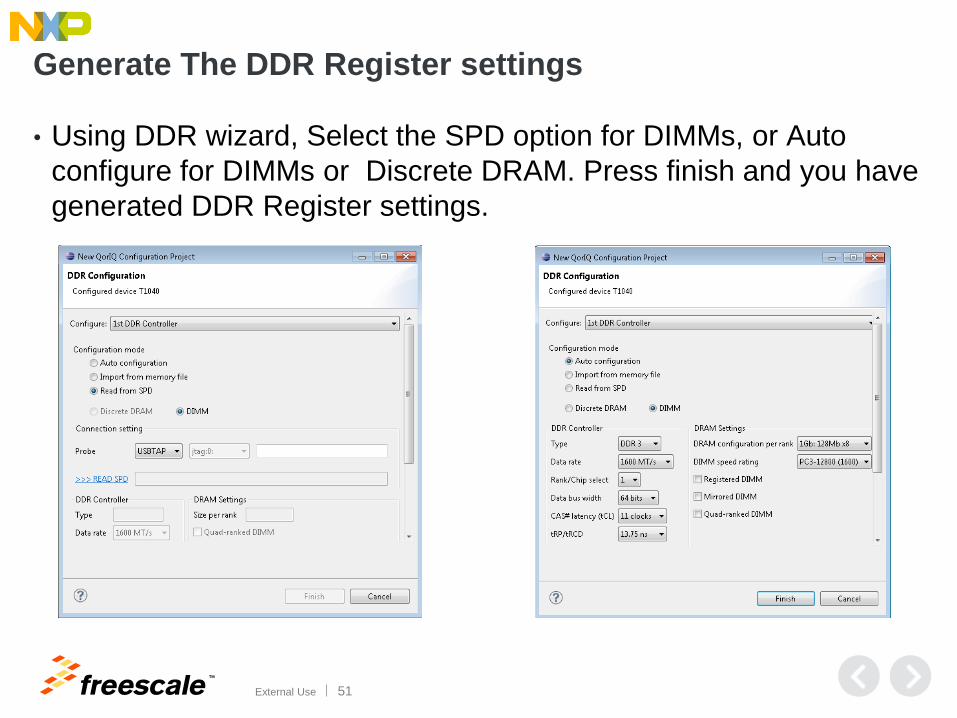
Generate The DDR Register settings
• Using DDR wizard, Select the SPD option for DIMMs, or Auto
configure for DIMMs or Discrete DRAM. Press finish and you have
generated DDR Register settings.

TM
External Use 52
Optimize/validate the DDR interface on your board
• The board dependent parameters are optimized by connecting to
your board and running targeted tests. After this stage, the DDR
interface in your board is optimized/validated.

TM
External Use 53
Summary

TM
External Use 54
Summary
• DDR3/3L is mainstream now.
• DDR4 is expected to gain market share in 2014 and become
mainstream by end of 2015
• T1 and LS1 devices support DDR3L and DDR4
• Most features of DDR3L and DDR4, such as write leveling,
ZQ calibration, ODT, DBI, C/A Parity, etc., are supported by the
memory controller in T1 & LS1 devices
• DDR4 offers higher densities, better reliability and low power
consumption in comparison to DDR3/3L.
• Follow JEDEC recommended topologies for discrete DRAM
• Using QCS DDRv tool configuration and initialization of memory
controller is easily achieved
TM
External Use 55
Useful References
• Books: − DRAM Circuit Design: A Tutorial, Brent Keeth and R. Jacob Baker, IEEE Press, 2001
• Freescale AppNotes: − AN2582 Hardware and Layout Design Considerations for DDR Memory Interfaces
− AN2910 Hardware and Layout Design Considerations for DDR2 Memory Interfaces
− AN2583 Programming the PowerQUICCIII / PowerQUICCII Pro DDR SDRAM Controller
− AN3369 PowerQUICC DDR2 SDRAM Controller Register Setting Considerations
− AN3939 PQ & QorIQ Interleaving
− AN3940 Layout Design Considerations for DDR3 Memory Interface
− AN4039 PowerQUICC DDR3 SDRAM Controller Register Setting Considerations
• Micron AppNotes: − TN-46-05 General DDR SDRAM Functionality
− TN-47-02 DDR2 Offers New Features and Functionality
− TN-47-01 DDR2 Design Guide
− TN-41-07 DDR3 Power-Up, Initialization, and Reset
− TN-41-08 DDR3 Design Guide
• JEDEC Specs: − JESD79E Double Data Rate (DDR) SDRAM Specification
− JESD79-2F DDR2 SDRAM Specification
− JESD79-3F DDR3 SDRAM Specification
− JESD79-4A DDR4 SDRAM Specification
• Tools − QCS DDRV tool
− http://www.freescale.com/webapp/sps/site/prod_summary.jsp?code=PE_QORIQ_DDRV
TM
External Use 56
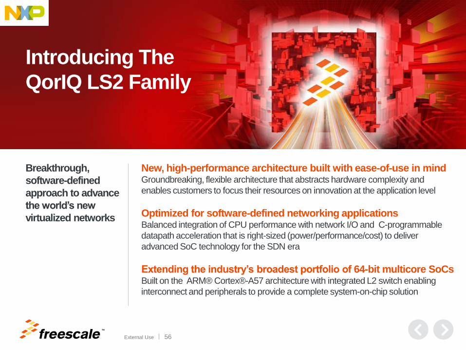
Introducing The
QorIQ LS2 Family
Breakthrough,
software-defined
approach to advance
the world’s new
virtualized networks
New, high-performance architecture built with ease-of-use in mind Groundbreaking, flexible architecture that abstracts hardware complexity and
enables customers to focus their resources on innovation at the application level
Optimized for software-defined networking applications Balanced integration of CPU performance with network I/O and C-programmable
datapath acceleration that is right-sized (power/performance/cost) to deliver
advanced SoC technology for the SDN era
Extending the industry’s broadest portfolio of 64-bit multicore SoCs Built on the ARM® Cortex®-A57 architecture with integrated L2 switch enabling
interconnect and peripherals to provide a complete system-on-chip solution

TM
External Use 57
QorIQ LS2 Family Key Features
Unprecedented performance and
ease of use for smarter, more
capable networks
High performance cores with leading
interconnect and memory bandwidth
• 8x ARM Cortex-A57 cores, 2.0GHz, 4MB L2
cache, w Neon SIMD
• 1MB L3 platform cache w/ECC
• 2x 64b DDR4 up to 2.4GT/s
A high performance datapath designed
with software developers in mind
• New datapath hardware and abstracted
acceleration that is called via standard Linux
objects
• 40 Gbps Packet processing performance with
20Gbps acceleration (crypto, Pattern
Match/RegEx, Data Compression)
• Management complex provides all
init/setup/teardown tasks
Leading network I/O integration
• 8x1/10GbE + 8x1G, MACSec on up to 4x 1/10GbE
• Integrated L2 switching capability for cost savings
• 4 PCIe Gen3 controllers, 1 with SR-IOV support
• 2 x SATA 3.0, 2 x USB 3.0 with PHY
SDN/NFV
Switching
Data
Center
Wireless
Access

TM
External Use 58
See the LS2 Family First in the Tech Lab!
4 new demos built on QorIQ LS2 processors:
Performance Analysis Made Easy
Leave the Packet Processing To Us
Combining Ease of Use with Performance
Tools for Every Step of Your Design

TM
© 2014 Freescale Semiconductor, Inc. | External Use
www.Freescale.com