Fundamental studies of titanium oxide–Pt(100) … · I. Stable high temperature structures formed...
19
Fundamental studies of titanium oxide–Pt(1 0 0) interfaces I. Stable high temperature structures formed by annealing TiO x films on Pt(1 0 0) Taketoshi Matsumoto 1 , Matthias Batzill 2 , Shuchen Hsieh 3 , Bruce E. Koel * Department of Chemistry, University of Southern California, Los Angeles, CA 90089-0482, United States Received 6 February 2004; accepted for publication 7 August 2004 Available online 25 August 2004 Abstract Surface structures formed by titanium oxide thin films at a Pt(1 0 0) surface have been studied by STM (scanning tunneling microscopy), LEED (low energy electron diffraction), AES (Auger electron spectroscopy), XPS (X-ray pho- toelectron spectroscopy), XPD (X-ray photoelectron diffraction) and He + -ISS (He + ion scattering spectrometry) in order to explore and elucidate stable high-temperature structures that may be formed at titania–Pt interfaces and pro- vide a basis for characterizing the chemistry of titania thin films on Pt(1 0 0). Titanium oxide films were produced by two different methods. First, titanium oxide films on Pt(1 0 0) were produced by oxidation using ozone (O 3 ) of a Pt 3 Ti sur- face alloy at 300 K and annealing at 1000 K. Smooth thin films with a (3 · 5) structure were observed at 1 ML (mono- layer) using this procedure, and we propose that the (3 · 5) structure is due to one layer of a Ti 2 O 3 film that is similar to the (1 · 2) strands formed on reduced TiO 2 (1 1 0) surfaces. Structures prepared by this method showed particularly ‘‘flat’’ terraces without islands. Second, TiO x films were formed by Ti evaporation and deposition on Pt(1 0 0) in 6.7 · 10 5 Pa O 2 and annealing the substrate above 750 K in vacuum. A (35) structure was produced also for these films below 1ML. A (4 · 3 p 5R60°) structure, referred to as the ‘‘24-structure’’, was observed after deposition of 2ML and after annealing at 850–1000 K. We propose a model for this structure composed of TiO 2 tetragonal nets with some O atoms in the second layer. The (4 · 3 p 5R60°) film changed to one with a (3 · 5) structure after annealing above 960 K in vacuum. TiO 2 clusters were observed in our investigations, but mainly after Ti deposition sufficient to form several monolayers and after annealing at 1000 K. Under those conditions, a small number of (3 · 5) domains were observed also, but it was surprising that clean (1 · 1)- and (5 · 20)-Pt(1 0 0) domains still existed over 2% of the surface. TiO 2 clusters decomposed to form a (2 p 2 · 2 p 2)R45° structure, which we propose to be Ti 5 O 8 , and (3 · 5) domains after annealing at 1300 K. Within our models, the composition of all titanium oxide ultrathin films on a Pt(1 0 0) surface are TiO 21.5 after 0039-6028/$ - see front matter Ó 2004 Elsevier B.V. All rights reserved. doi:10.1016/j.susc.2004.08.006 * Corresponding author. Tel.: +213 740 4126; fax: +213 740 3972. E-mail address: [email protected] (B.E. Koel). 1 Present address: Laboratory for Entrepreneurship, University of Tsukuba, Ibaraki 305-8573, Japan. 2 Present address: Department of Physics, Tulane University, New Orleans, LA 70118, United States. 3 Present address: NIST, Gaithersburg, MD 20899, Unites States. Surface Science 572 (2004) 127–145 www.elsevier.com/locate/susc
Transcript of Fundamental studies of titanium oxide–Pt(100) … · I. Stable high temperature structures formed...

Surface Science 572 (2004) 127–145
www.elsevier.com/locate/susc
Fundamental studies of titanium oxide–Pt(100) interfacesI. Stable high temperature structures formed by annealing
TiOx films on Pt(100)
Taketoshi Matsumoto 1, Matthias Batzill 2, Shuchen Hsieh 3, Bruce E. Koel *
Department of Chemistry, University of Southern California, Los Angeles, CA 90089-0482, United States
Received 6 February 2004; accepted for publication 7 August 2004
Available online 25 August 2004
Abstract
Surface structures formed by titanium oxide thin films at a Pt(100) surface have been studied by STM (scanning
tunneling microscopy), LEED (low energy electron diffraction), AES (Auger electron spectroscopy), XPS (X-ray pho-
toelectron spectroscopy), XPD (X-ray photoelectron diffraction) and He+-ISS (He+ ion scattering spectrometry) in
order to explore and elucidate stable high-temperature structures that may be formed at titania–Pt interfaces and pro-
vide a basis for characterizing the chemistry of titania thin films on Pt(100). Titanium oxide films were produced by two
different methods. First, titanium oxide films on Pt(100) were produced by oxidation using ozone (O3) of a Pt3Ti sur-
face alloy at 300K and annealing at 1000K. Smooth thin films with a (3 · 5) structure were observed at 1ML (mono-
layer) using this procedure, and we propose that the (3 · 5) structure is due to one layer of a Ti2O3 film that is similar to
the (1 · 2) strands formed on reduced TiO2(110) surfaces. Structures prepared by this method showed particularly
‘‘flat’’ terraces without islands. Second, TiOx films were formed by Ti evaporation and deposition on Pt(100) in
6.7 · 10�5Pa O2 and annealing the substrate above 750K in vacuum. A (35) structure was produced also for these films
below �1ML. A (4 · 3p5R60�) structure, referred to as the ‘‘24-structure’’, was observed after deposition of �2ML
and after annealing at 850–1000K. We propose a model for this structure composed of TiO2 tetragonal nets with some
O atoms in the second layer. The (4 · 3p5R60�) film changed to one with a (3 · 5) structure after annealing above 960K
in vacuum. TiO2 clusters were observed in our investigations, but mainly after Ti deposition sufficient to form several
monolayers and after annealing at 1000K. Under those conditions, a small number of (3 · 5) domains were observed also,
but it was surprising that clean (1 · 1)- and (5 · 20)-Pt(100) domains still existed over �2% of the surface. TiO2 clusters
decomposed to form a (2p2 · 2
p2)R45� structure, which we propose to be Ti5O8, and (3 · 5) domains after annealing at
1300K. Within our models, the composition of all titanium oxide ultrathin films on a Pt(100) surface are TiO2�1.5 after
0039-6028/$ - see front matter � 2004 Elsevier B.V. All rights reserved.
doi:10.1016/j.susc.2004.08.006
* Corresponding author. Tel.: +213 740 4126; fax: +213 740 3972.
E-mail address: [email protected] (B.E. Koel).1 Present address: Laboratory for Entrepreneurship, University of Tsukuba, Ibaraki 305-8573, Japan.2 Present address: Department of Physics, Tulane University, New Orleans, LA 70118, United States.3 Present address: NIST, Gaithersburg, MD 20899, Unites States.

128 T. Matsumoto et al. / Surface Science 572 (2004) 127–145
annealing at 850–1300K. Chemical changes occurring during annealing of titanium oxide films include Ti dissolution
(alloying) into the bulk of the Pt(100) crystal. We suggest that these results will have important consequences for the
understanding and modeling of catalysis of related systems.
� 2004 Elsevier B.V. All rights reserved.
Keywords: Low energy electron diffraction (LEED); Low energy ion scattering (LEIS); Scanning tunneling microscopy; X-ray
photoelectron spectroscopy; Epitaxy; Platinum; Titanium oxide
1. Introduction
Many metal catalysts are dispersed on oxide
supports, and SMSI (strong metal support interac-
tion) has been reported as an important effect to
alter their catalytic behavior [1]. Pt/TiO2 catalysts
are typical systems exhibiting SMSI for CO hydro-
genation after high temperature reduction. Re-
duced Pt/TiO2 surfaces have been investigated
using many techniques, including XPS (X-ray pho-toelectron spectroscopy), AES (Auger electron
spectroscopy), XRD (X-ray diffraction), NMR
(nuclear magnetic resonance), IR (infrared spectr-
oscopy), ISS (ion scattering spectrometry), and
EXAFS (extended X-ray absorption fine structure)
[1–6]. These studies lead to the conclusion that a
reduced titania (TiO1.5�0.9) film covers Pt surfaces
and this suppresses CO and H2 chemisorption.SMSI has also been reported for Pt/TiO2 catalysts
used for the selective hydrogenation of crotonalde-
hyde [7,8].
Some researchers have also been concerned
with Ti diffusion into the Pt clusters on the cata-
lysts. The possibility of Pt–Ti alloy formation
was suggested by Pt 4f peak shifts or narrowing
in XPS spectra or characteristic EXAFS peaks.These results were observed for Pt clusters pro-
duced from Pt films deposited on TiO2 [3,9,10],
Pt clusters on carbon black impregnated with
TiO2 [11], a Pt + TiO2 co-sputtered sample [10],
and Pt clusters formed on TiO2/Ti(0001) [12],
but not for 2% Pt clusters supported on TiO2 pow-
der [13]. Investigations of polycrystalline Pt sur-
faces containing TiOx films have produced mixedresults [6,14]. Theoretical analysis has also sug-
gested Pt–Ti alloy formation [15,16], but experi-
ments have not yet provided a decisive answer to
questions about the conditions required for
alloying.
A few STM (scanning tunneling microscopy)
experiments have been attempted to observe thinfilms of titanium oxide on Pt surfaces and Pt active
sites with SMSI at atomic resolution. Two ordered
structures of TiO2 and Ti4O7 were found on
Pt(111) that were similar to the rutile TiO2(110)
surface [2]. Deposition of Pt on TiO2(110) and
annealing in vacuum formed TiO1.1 films on flat
(111) tops of Pt clusters [17,18]. It was also sug-
gested that active Pt sites might be the sides ofPt clusters floating on TiO2-like ‘‘icebergs’’. How-
ever, titanium oxide thin films on Pt(100) or
Pt(110) have not been studied. In related studies,
AES and LEED (low electron energy diffraction)
experiments have indicated TiO, TiO1.2, and
TiO2 thin films on Pt3Ti(111) and (100) bulk alloy
surfaces after annealing in O2 [19]. Another study
on Pt3Ti(111) using XPS indicated formation ofTiO2 following O2 oxidation below 673K and
Ti2O3 after oxidation above 723K [20].
The clean Pt(100) surface is known to recon-
struct to a hexagonal (5 · 20) structure after
annealing to 1000K [21]. The first layer of the
(5 · 20)-Pt(100) surface contains an excess atomic
density of �20% over that of the second layer in
the (1 · 1) structure [22]. This reconstruction islifted, with the excess Pt atoms incorporated into
the adlayer, with the adsorption of CO, H, O
[23–25] and C2H4 [26] at 300K or the deposition
of other materials such as Sn [27], Ag [28], Sm
[29], Ge [30], Ti [31] and FeO [32]. Such deposition
can give islands, ‘‘flat’’ alloys with square struc-
tures, or a flat (1 · 1)-Pt(100) substrate.
In this study, oxidation of a Pt3Ti surface alloyand deposition of Ti in an O2 ambient were used to
create ultrathin films of titanium oxide on a
Pt(100) crystal substrate. These surfaces were
characterized by STM, LEED, AES, XPS, XPD
(X-ray photoelectron diffraction) and He+-ISS

T. Matsumoto et al. / Surface Science 572 (2004) 127–145 129
(He+ ion scattering spectrometry) under varying
conditions of film thickness and annealing temper-
ature. While speculative, we have proposed some
reasonable structural models for these films. Ther-
mal stability of the titanium oxide films is alsodiscussed.
2. Experimental
Experiments were carried out by using the same
single crystal in two UHV (ultra high vacuum)
chambers. One chamber was equipped withSTM, LEED and AES [33], and the other with
LEED, ISS, XPS, and XPD [34]. The clean
Pt(100) surface was prepared by many cycles of
Ar+-ion sputtering and annealing in O2 and flash-
ing to 1000K in vacuum. The clean surface was
checked by STM, LEED, AES, and/or XPS. Tita-
nium was evaporated from a Ti rod by electron
bombardment after outgassing for 10min, andAES and XPS subsequent to the deposition
showed a clean Ti film with good reproducibility.
AES ratios of Pt, Ti, and O were obtained by
using the peak-to-peak heights of the Pt(237eV),
Ti(387eV) and O(510eV) transitions obtained in
dN/dE spectra. Sensitivity ratios for these peaks
is estimated to be 1:2:2.4 for Pt:Ti:O [35]. All
STM images were acquired in constant-currentmode with the sample at 300K. The coverage
where one layer of a TiOx film effectively covers
the Pt(100) substrate, as determined by STM is
defined to be 1ML. As discussed later, this condi-
tion is also where TiO2 assigned to the second
layer starts to be detected in XPS.
Fig. 1. LEED pattern and STM topographs of the c(2 · 2)-
Pt3Ti surface alloy on Pt(100). The Pt3Ti surface alloy was
produced by Ti deposition on Pt(100) at 300K and annealing
at 900K: (a) LEED pattern and (b) STM topograph
(Vs = 0.04V, It = 2.4 nA). The inset shows an area scanned at
an expanded scale (Vs = 0.33V, It = 1.3 nA). The superimposed
rectangle indicates one unit cell.
3. Results
3.1. Oxidation of a Pt3Ti surface alloy on Pt(100)
Oxide thin films with a coverage near 1ML
were easily produced by 6L O3 (ozone) oxidation
of a Pt3Ti surface alloy on Pt(100), denoted as
Pt3Ti/Pt(100), at 300K. The clean Pt3Ti surface
alloy was produced before oxidation by Ti evapo-
ration on Pt(100) and annealing to 900K in vac-
uum. The AES ratio of Pt/Ti was 1/2. LEED
showed a c(2 · 2) pattern (Fig. 1(a)), and STM
images (Fig. 1(b)) reveal homogeneous c(2 · 2) ter-
races with sizes smaller than �30nm. Some small
pits and bumps (possibly due to TiC [36]) can also
be observed.After annealing such an oxide film to 800–900K,
LEED showed a (4 · 3p5)R60� pattern as seen in
Fig. 2(a) and simulated in Fig. 2(b). This unit cell
is 24 times larger than that of (1 · 1)-Pt(100),
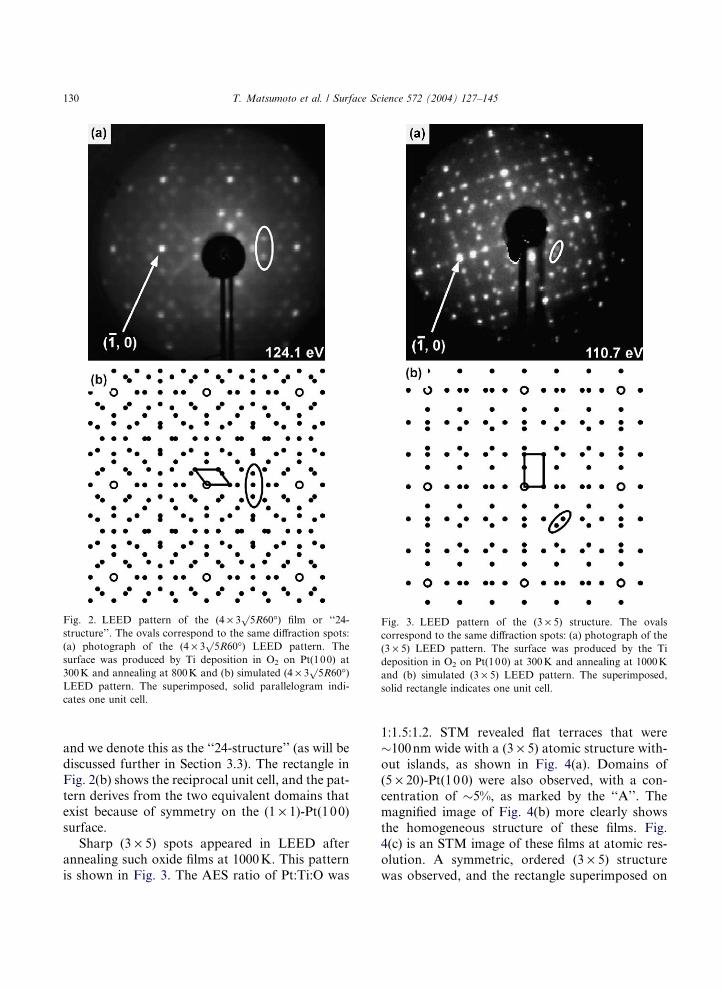
Fig. 2. LEED pattern of the (4 · 3p5R60�) film or ‘‘24-
structure’’. The ovals correspond to the same diffraction spots:
(a) photograph of the (4 · 3p5R60�) LEED pattern. The
surface was produced by Ti deposition in O2 on Pt(100) at
300K and annealing at 800K and (b) simulated (4 · 3p5R60�)
LEED pattern. The superimposed, solid parallelogram indi-
cates one unit cell.
Fig. 3. LEED pattern of the (3 · 5) structure. The ovals
correspond to the same diffraction spots: (a) photograph of the
(3 · 5) LEED pattern. The surface was produced by the Ti
deposition in O2 on Pt(100) at 300K and annealing at 1000K
and (b) simulated (3 · 5) LEED pattern. The superimposed,
solid rectangle indicates one unit cell.
130 T. Matsumoto et al. / Surface Science 572 (2004) 127–145
and we denote this as the ‘‘24-structure’’ (as will be
discussed further in Section 3.3). The rectangle in
Fig. 2(b) shows the reciprocal unit cell, and the pat-tern derives from the two equivalent domains that
exist because of symmetry on the (1 · 1)-Pt(100)
surface.
Sharp (3 · 5) spots appeared in LEED after
annealing such oxide films at 1000K. This pattern
is shown in Fig. 3. The AES ratio of Pt:Ti:O was
1:1.5:1.2. STM revealed flat terraces that were
�100nm wide with a (3 · 5) atomic structure with-
out islands, as shown in Fig. 4(a). Domains of
(5 · 20)-Pt(100) were also observed, with a con-
centration of �5%, as marked by the ‘‘A’’. Themagnified image of Fig. 4(b) more clearly shows
the homogeneous structure of these films. Fig.
4(c) is an STM image of these films at atomic res-
olution. A symmetric, ordered (3 · 5) structure
was observed, and the rectangle superimposed on

Fig. 4. STM topographs of a flat (3 · 5) oxide film surface. The surface was prepared by a 6L O3 exposure on the Pt3Ti surface alloy at
300K and annealing at 1000K. The superimposed rectangles indicate one unit cell: (a) large (3 · 5) terrace (B) and bare-Pt(100)
domain (A). (Vs = 0.46V, It = 1.1 nA); (b) homogeneous terrace (Vs = 0.06V, It = 2.1 nA); (c) (3 · 5) structure at atomic resolution.
(Vs = 0.7V, It = 0.63nA).
T. Matsumoto et al. / Surface Science 572 (2004) 127–145 131
the image shows this unit cell. The apparent corru-
gation of this structure was small, only 0.03nm.Oxidation with 1000L O2 rather than O3 resulted
in a similar LEED pattern but many spots were
broad or missing.
3.2. TiOx deposition on Pt(100) to form a (3 · 5)
structure
Titanium oxide films with a (3 · 5) structurewere produced by deposition of Ti on Pt(100) at
300K in an O2 ambient of 6.7 · 10�5Pa and
annealing in vacuum. After deposition and anneal-
ing below 750K, a (1 · 1) LEED pattern appeared
with diffuse spots. Annealing at 750–850K pro-
duced additional LEED spots which became shar-
per by heating above 900K. An STM topographof such a (3 · 5) film with a coverage of 0.3ML
is shown in Fig. 5(a). The Pt:Ti:O AES ratio of this
surface was 1:1:1. The LEED pattern showed a
mixture of (3 · 5) and (5 · 20) spots. STM images
revealed patches of oxide wider than 50nm on flat
terraces. A line scan shown in Fig. 5(a) is given
below the STM image and a model is provided
to interpret this cross-section of the surface. Fig.5(b) provides an expanded view of the highlighted
square area in Fig. 5(a). A rectangle indicating the
(3 · 5) unit cell is superimposed on this image. In
Fig. 5(a), domains B1, B2, and B3 are assigned
to the (3 · 5) oxide film and the region A1 is
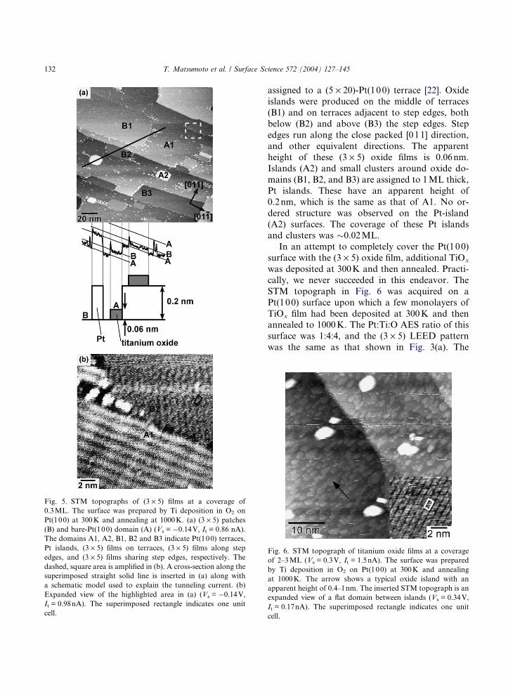
Fig. 5. STM topographs of (3 · 5) films at a coverage of
0.3ML. The surface was prepared by Ti deposition in O2 on
Pt(100) at 300K and annealing at 1000K. (a) (3 · 5) patches
(B) and bare-Pt(100) domain (A) (Vs = �0.14V, It = 0.86 nA).
The domains A1, A2, B1, B2 and B3 indicate Pt(100) terraces,
Pt islands, (3 · 5) films on terraces, (3 · 5) films along step
edges, and (3 · 5) films sharing step edges, respectively. The
dashed, square area is amplified in (b). A cross-section along the
superimposed straight solid line is inserted in (a) along with
a schematic model used to explain the tunneling current. (b)
Expanded view of the highlighted area in (a) (Vs = �0.14V,
It = 0.98nA). The superimposed rectangle indicates one unit
cell.
132 T. Matsumoto et al. / Surface Science 572 (2004) 127–145
assigned to a (5 · 20)-Pt(100) terrace [22]. Oxide
islands were produced on the middle of terraces
(B1) and on terraces adjacent to step edges, both
below (B2) and above (B3) the step edges. Step
edges run along the close packed [011] direction,and other equivalent directions. The apparent
height of these (3 · 5) oxide films is 0.06nm.
Islands (A2) and small clusters around oxide do-
mains (B1, B2, and B3) are assigned to 1ML thick,
Pt islands. These have an apparent height of
0.2nm, which is the same as that of A1. No or-
dered structure was observed on the Pt-island
(A2) surfaces. The coverage of these Pt islandsand clusters was �0.02ML.
In an attempt to completely cover the Pt(100)
surface with the (3 · 5) oxide film, additional TiOx
was deposited at 300K and then annealed. Practi-
cally, we never succeeded in this endeavor. The
STM topograph in Fig. 6 was acquired on a
Pt(100) surface upon which a few monolayers of
TiOx film had been deposited at 300K and thenannealed to 1000K. The Pt:Ti:O AES ratio of this
surface was 1:4:4, and the (3 · 5) LEED pattern
was the same as that shown in Fig. 3(a). The
Fig. 6. STM topograph of titanium oxide films at a coverage
of 2–3ML (Vs = 0.3V, It = 1.5nA). The surface was prepared
by Ti deposition in O2 on Pt(100) at 300K and annealing
at 1000K. The arrow shows a typical oxide island with an
apparent height of 0.4–1nm. The inserted STM topograph is an
expanded view of a flat domain between islands (Vs = 0.34V,
It = 0.17nA). The superimposed rectangle indicates one unit
cell.

Fig. 8. XPD spectra of a (3 · 5) oxide film with a coverage near
1.2ML. Angle-resolved Pt 4f7/2, Ti 2p3/2 and O 1s photoelectron
intensities were observed along the (a) [011] and (b) [001]
azimuths.
T. Matsumoto et al. / Surface Science 572 (2004) 127–145 133
STM image of this surface (Fig. 6) showed many
islands which had disordered structures. The
apparent height of these islands was 0.4 to 1nm
higher than that of the (3 · 5) oxide surface, indi-
cating that the islands have a thickness of severallayers of titanium oxide. The inset in Fig. 6 reveals
a (3 · 5) terrace between islands. The superim-
posed rectangle indicates a (3 · 5) unit cell. If the
surface was only annealed to 850K, in contrast
to the behavior for lower coverage oxide films,
we observed the 24-structure.
We used He+-ISS to characterize a titanium
oxide film that just covered the Pt substrate.He+-ISS reveals uniquely the composition of
the outermost layer of the substrate. The TiOx
coverage after deposition and annealing to
1000K was determined to be �1.2ML from XP
spectra (as discussed in Section 3.4). LEED
showed a sharp (3 · 5) pattern. Fig. 7 shows that
the Pt peak at E/E0 � 0.9 is completely elimi-
nated for the oxide-covered surface and only Ti
Fig. 7. He+-ion scattering spectra from (top) a (3 · 5) oxide
film with a coverage near 1.2ML and (bottom) clean Pt(100)
surface.
(E/E0 � 0.7) and O (E/E0 � 0.35) peaks were ob-
served. This establishes that the outmost layer of
the (3 · 5) oxide surface consists of only Ti and
O atoms.
For the identical oxide surface, XPD spectra
were also obtained along the [011], [032], [031]
and [010] azimuths. Fig. 8(a) and (b) provide theXPD spectra for the [011] and [010] azimuths.
No forward scattering peaks for Ti(2p) or O(1s)
photoelectrons were observed, and the Pt(4f) for-
ward scattering peaks were similar to those for
the clean Pt(100) surface (not shown). Data ac-
quired for the [032] and [031] azimuths were con-
sistent with these observations. Because we know
that the oxide surface has an ordered structure,these results indicate that the (3 · 5) oxide film is
only one layer thick [37]. These data also eliminate
any substantial concentration of Ti in the near-
subsurface region, due to appreciable alloying with
Pt [31], under these conditions.
Heating any coverage of the (3 · 5) oxide film in
an ambient of 6.7 · 10�5Pa O2 to give a 100L O2
exposure with the surface at 300–1000K made nosignificant difference in either the LEED or STM
results.
134 T. Matsumoto et al. / Surface Science 572 (2004) 127–145
3.3. TiOx deposition on Pt(100) to form a
(4 · 3p5R60�) structure
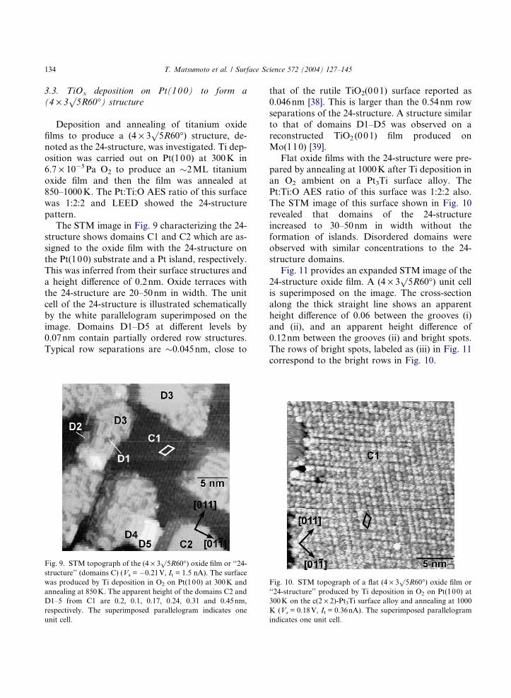
Deposition and annealing of titanium oxide
films to produce a (4 · 3p5R60�) structure, de-
noted as the 24-structure, was investigated. Ti dep-
osition was carried out on Pt(100) at 300K in
6.7 · 10�5Pa O2 to produce an �2ML titanium
oxide film and then the film was annealed at
850–1000K. The Pt:Ti:O AES ratio of this surface
was 1:2:2 and LEED showed the 24-structure
pattern.
The STM image in Fig. 9 characterizing the 24-structure shows domains C1 and C2 which are as-
signed to the oxide film with the 24-structure on
the Pt(100) substrate and a Pt island, respectively.
This was inferred from their surface structures and
a height difference of 0.2nm. Oxide terraces with
the 24-structure are 20–50nm in width. The unit
cell of the 24-structure is illustrated schematically
by the white parallelogram superimposed on theimage. Domains D1–D5 at different levels by
0.07nm contain partially ordered row structures.
Typical row separations are �0.045nm, close to
Fig. 9. STM topograph of the (4 · 3p5R60�) oxide film or ‘‘24-
structure’’ (domains C) (Vs = �0.21V, It = 1.5 nA). The surface
was produced by Ti deposition in O2 on Pt(100) at 300K and
annealing at 850K. The apparent height of the domains C2 and
D1–5 from C1 are 0.2, 0.1, 0.17, 0.24, 0.31 and 0.45nm,
respectively. The superimposed parallelogram indicates one
unit cell.
that of the rutile TiO2(001) surface reported as
0.046nm [38]. This is larger than the 0.54nm row
separations of the 24-structure. A structure similar
to that of domains D1–D5 was observed on a
reconstructed TiO2(001) film produced onMo(110) [39].
Flat oxide films with the 24-structure were pre-
pared by annealing at 1000K after Ti deposition in
an O2 ambient on a Pt3Ti surface alloy. The
Pt:Ti:O AES ratio of this surface was 1:2:2 also.
The STM image of this surface shown in Fig. 10
revealed that domains of the 24-structure
increased to 30–50nm in width without theformation of islands. Disordered domains were
observed with similar concentrations to the 24-
structure domains.
Fig. 11 provides an expanded STM image of the
24-structure oxide film. A (4 · 3p5R60�) unit cell
is superimposed on the image. The cross-section
along the thick straight line shows an apparent
height difference of 0.06 between the grooves (i)and (ii), and an apparent height difference of
0.12nm between the grooves (ii) and bright spots.
The rows of bright spots, labeled as (iii) in Fig. 11
correspond to the bright rows in Fig. 10.
Fig. 10. STM topograph of a flat (4 · 3p5R60�) oxide film or
‘‘24-structure’’ produced by Ti deposition in O2 on Pt(100) at
300K on the c(2 · 2)-Pt3Ti surface alloy and annealing at 1000
K (Vs = 0.18V, It = 0.36nA). The superimposed parallelogram
indicates one unit cell.
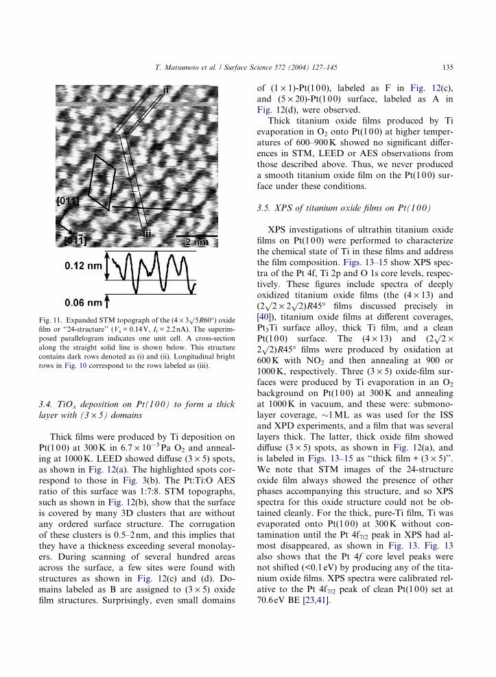
Fig. 11. Expanded STM topograph of the (4 · 3p5R60�) oxide
film or ‘‘24-structure’’ (Vs = 0.14V, It = 2.2nA). The superim-
posed parallelogram indicates one unit cell. A cross-section
along the straight solid line is shown below. This structure
contains dark rows denoted as (i) and (ii). Longitudinal bright
rows in Fig. 10 correspond to the rows labeled as (iii).
T. Matsumoto et al. / Surface Science 572 (2004) 127–145 135
3.4. TiOx deposition on Pt(100) to form a thick
layer with (3 · 5) domains
Thick films were produced by Ti deposition on
Pt(100) at 300K in 6.7 · 10�5Pa O2 and anneal-
ing at 1000K. LEED showed diffuse (3 · 5) spots,
as shown in Fig. 12(a). The highlighted spots cor-
respond to those in Fig. 3(b). The Pt:Ti:O AES
ratio of this surface was 1:7:8. STM topographs,
such as shown in Fig. 12(b), show that the surfaceis covered by many 3D clusters that are without
any ordered surface structure. The corrugation
of these clusters is 0.5–2nm, and this implies that
they have a thickness exceeding several monolay-
ers. During scanning of several hundred areas
across the surface, a few sites were found with
structures as shown in Fig. 12(c) and (d). Do-
mains labeled as B are assigned to (3 · 5) oxidefilm structures. Surprisingly, even small domains
of (1 · 1)-Pt(100), labeled as F in Fig. 12(c),
and (5 · 20)-Pt(100) surface, labeled as A in
Fig. 12(d), were observed.
Thick titanium oxide films produced by Ti
evaporation in O2 onto Pt(100) at higher temper-atures of 600–900K showed no significant differ-
ences in STM, LEED or AES observations from
those described above. Thus, we never produced
a smooth titanium oxide film on the Pt(100) sur-
face under these conditions.
3.5. XPS of titanium oxide films on Pt(100)
XPS investigations of ultrathin titanium oxide
films on Pt(100) were performed to characterize
the chemical state of Ti in these films and address
the film composition. Figs. 13–15 show XPS spec-
tra of the Pt 4f, Ti 2p and O 1s core levels, respec-
tively. These figures include spectra of deeply
oxidized titanium oxide films (the (4 · 13) and
(2p2 · 2
p2)R45� films discussed precisely in
[40]), titanium oxide films at different coverages,
Pt3Ti surface alloy, thick Ti film, and a clean
Pt(100) surface. The (4 · 13) and (2p2 ·
2p2)R45� films were produced by oxidation at
600K with NO2 and then annealing at 900 or
1000K, respectively. Three (3 · 5) oxide-film sur-
faces were produced by Ti evaporation in an O2
background on Pt(100) at 300K and annealingat 1000K in vacuum, and these were: submono-
layer coverage, �1ML as was used for the ISS
and XPD experiments, and a film that was several
layers thick. The latter, thick oxide film showed
diffuse (3 · 5) spots, as shown in Fig. 12(a), and
is labeled in Figs. 13–15 as ‘‘thick film + (3 · 5)’’.
We note that STM images of the 24-structure
oxide film always showed the presence of otherphases accompanying this structure, and so XPS
spectra for this oxide structure could not be ob-
tained cleanly. For the thick, pure-Ti film, Ti was
evaporated onto Pt(100) at 300K without con-
tamination until the Pt 4f7/2 peak in XPS had al-
most disappeared, as shown in Fig. 13. Fig. 13
also shows that the Pt 4f core level peaks were
not shifted (<0.1eV) by producing any of the tita-nium oxide films. XPS spectra were calibrated rel-
ative to the Pt 4f7/2 peak of clean Pt(100) set at
70.6eV BE [23,41].

Fig. 12. LEED pattern and STM topographs of a Pt(100) surface covered with titanium oxide films at 3–10ML: (a) observed (3 · 5)
LEED pattern. The highlighted spots correspond to those in Fig. 3; (b) STM topograph of TiOx clusters (Vs = 0.08V, It = 2.1 nA); (c)
STM topograph of the (3 · 5) (B) and (1 · 1) (F) domains (Vs = 0.34V, It = 0.41 nA); (d) STM topograph of the (5 · 20)-Pt(100)
domain (Vs = 0.34V, It = 0.46nA).
136 T. Matsumoto et al. / Surface Science 572 (2004) 127–145
Fig. 14 provides information on the Ti 2p corelevels for a number of surfaces, and this data is
summarized in Table 1. The Ti 2p3/2 peak at
453.6eV BE for the thick, pure-Ti film was within
0.1eV of that reported previously for thick, heter-
ogeneous Ti metal films [43]. The (4 · 13) oxide
film showed a broad Ti 2p3/2 peak at 457.6eV
BE, and this is assignable to Ti4+ based on previ-
ous studies as indicated by the dark band at thetop of the figure. Two peaks at 457.8 and
455.7eV BE were observed for the (2p2 ·
2p2)R45� structure which we assign to Ti4+ and
Ti3+, respectively. Peaks from Ti3+ were found at
455.9–455.6eV BE for all of the (3 · 5) oxide films,
and peaks from Ti4+ appeared at 458.7–458.1eVBE with increasing coverage. Thus, we assign the
(4 · 13) structure to TiO2, (2p2 · 2
p2)R45� struc-
ture to TiO2�1.5, (3 · 5) structure to Ti2O3 and
thick oxide islands to TiO2 with possibly some
Ti2O3. The coverage of the (3 · 5) oxide film that
was used for the ISS and XPD experiments can
be estimated to be �1.2ML from the Ti4+ to
Ti3+ peak ratio in the middle curve of Fig. 14.The O 1s spectra shown in Fig. 15 from four
different oxide films, i.e., (4 · 13), (2p2 ·
2p2)R45�, submonolayer (3 · 5) and thick oxide
film, gave peaks at 529.9–529.1eV BE, with widths
of 1.4, 1.5, 2.0 and 1.1eV FWHM, respectively.

Fig. 13. Pt 4f XPS spectra of several titanium oxide films, thick
Ti film, and clean (5 · 20)-Pt(100) surface. The (4 · 13) and
(2p2 · 2
p2)R45� films were produced by NO2 oxidation of the
(3 · 5) surface at 300K, and then annealing at 900 and 1000K,
respectively. Titanium oxide films were produced by Ti evap-
oration in O2 on Pt(100) at 300K and annealing at 1000K. The
thick Ti film was evaporated onto Pt(100) at 300K.
T. Matsumoto et al. / Surface Science 572 (2004) 127–145 137
Both of the Ti4+ 2p and O 1s peaks shifted to
higher binding energy for the thick film by 0.6–
0.9eV.
Fig. 14. Ti 2p XPS spectra of several titanium oxide films,
c(2 · 2)-Pt3 Ti/Pt(100) surface alloy, thick Ti film, and clean
(5 · 20)-Pt(100) surface. The Pt3Ti surface alloy was prepared
by Ti evaporation on Pt(100) at 300K and annealing at 900K.
3.6. Thermal stability of titanium oxide films
The thermal stability of an ultrathin titanium
oxide film on a Pt(100) substrate was studied with
AES, LEED and STM. This involved a titanium
oxide film with a coverage of �2ML produced
by Ti deposition in an O2 ambient on Pt(100)and annealing in vacuum. Following deposition,
only a disordered structure was observed in
LEED. The LEED pattern of the 24-structure
was observed after annealing at 850K. Fig. 16
summarizes changes observed in the AES ratios
of Ti/Pt, O/Pt and O/Ti after annealing. Heating
to 850K only changed the Ti/Pt ratio, indicating
that excess Ti dissolved into the bulk [45]. Anneal-ing at 1000 and 1200K caused the appearance of
the (3 · 5) LEED pattern and disordered TiO2
clusters (as shown in the STM images in Fig. 6).

Fig. 15. O 1s XPS spectra of several titanium oxide films, thick
Ti film and clean (5 · 20)-Pt(100) surface.
138 T. Matsumoto et al. / Surface Science 572 (2004) 127–145
This further decreases the Ti/Pt AES ratio, and
also now a large change in the O/Pt AES ratio.
Heating to 1300K formed the (2p2 · 2
p2)R45�
LEED pattern [38]. STM topographs showed
Table 1
Ti 2p3/2 core level binding energies in XPS
Species Material
Ti4+ (4 · 13)-TiO2/Pt(100)
(2p2 · 2
p2)R45�-Ti5O8/Pt(100)
Thick TiO2 islands/Pt(100)
TiO2/Pt(111)
TiO2/Pt foil
TiO2 (bulk)
Ti3+ (3 · 5)-Ti2O3/Pt(100)
Ti4O7/Pt(111)
TiOx/Pt foil
Ti2O3 (bulk)
Ti2+ TiO (bulk)
Pt3Ti surface alloy Pt3Ti/Pt(100)
Pt3Ti/Pt(111)
Pt3Ti alloy Pt3Ti (bulk)
Ti Thick Ti film/Pt(100)
Ti (bulk)
fewer TiO2 clusters and more (5 · 20)-Pt(100) area
along with (3 · 5) and (2p2 · 2
p2)R45� domains.
This behavior was also observed for the thick
films, as seen in Figs. 6 and 12. However,
(2p2 · 2
p2)R45� domains were not observed after
annealing the flat 24-structure to 1300K, as shown
in Fig. 10.
We attempted to perform TPD on these sam-
ples, but no clear O2 or Ti desorption peak was
observed prior to 1300K was seen, although a
large increase in the background signals occurred
near 1200K and this could possibly indicate
some desorption from the sample. This differsfrom O2 TPD results from SnOx/Pt(111) [44]
where O2 desorption peaks were observed prior
to 1200K.
4. Discussion
Our goals include identifying the stable, high-temperature structures that are formed by heating
TiOx films at Pt(100) surfaces. Elucidation of the
chemical state of Ti in these films is essential in this
regard. We begin our discussion of the characteri-
zation and structure of these films by considering
the results from XPS.
Binding energy (eV) Reference
457.6 This work
457.8 This work
458.7–458.1 This work
458.4 [2]
458.6–457.9 [6]
459.0 [42]
455.9–455.6 This work
456.2 [2]
456.6 [6]
457.5 [42]
455.3 [42]
454.5 [31]
455.2, 455.6 [41]
455.0 [42]
453.6 This work
453.7 [42]

Fig. 16. Influence of temperature on the AES ratios for Ti/Pt,
O/Pt and O/Ti of a titanium oxide film on Pt(100). The
observed LEED patterns are also indicated.
T. Matsumoto et al. / Surface Science 572 (2004) 127–145 139
4.1. Chemical state identification from XPS
4.1.1. Ti binding energies in alloy and oxide films on
Pt
Alloying Ti with Pt causes an increase in the Ti
2p3/2 peak binding energy compared to that in Ti
metal, apparently due to an increase in oxidation
state of the Ti. Pt–Ti alloys are formed with elec-
tron transfer from Ti to Pt [36,56].
Reactions of Ti with oxygen to form titaniumoxides increase the Ti oxidation state to Ti2+,
Ti3+ and Ti4+, and further increase the Ti 2p3/2peak binding energy. Identification of small
amounts of Ti2+, or TiO, is difficult in Pt–Ti bime-
tallic systems because of the difficulty in distin-
guishing this phase from the Pt–Ti alloy phase on
the basis of the Ti 2p3/2 peak binding energy. How-
ever, TiO is not a major species in any of the TiOx
films that we prepared and investigated on Pt(100).
Based on XPS, we conclude that Ti3+, or Ti2O3,
comprises most of the (3 · 5) structure on Pt(100).
Also, XPS indicates that that Ti4+, or TiO2, com-
prises most of the (4 · 13) structure on Pt(100).
Spectra from the (2p2 · 2
p2)R45� structure
showed two peaks, both Ti3+ and Ti4+, and this
oxide film is assigned to TiO2�1.5. Thick oxide is-lands are assigned to TiO2 with possibly some
Ti2O3.
The Ti 2p peaks for the (4 · 13), (2p2 ·
2p2)R45� and submonolayer (3 · 5) films showed
lower binding energies by 0.2–0.6eV than those of
TiO2 and Ti4O7 films on Pt(111) [2]. The O 1s XPS
peaks also appeared at 530.6eV for TiO2(110) [57]
and 530.2–529.6eV for thin TiOx films on a Pt
polycrystalline sample [6], and at 529.9–529.1eVfor TiO2�1.5/Pt(100). The titanium oxide films on
Pt(111) were two-layer films, and the lower bind-
ing energies that we observed for monolayer oxide
films on Pt(100) implies either that the oxide films
on Pt(100) are more reduced oxide phases or in-
creased final-state screening effect occur in the
monolayer films.
We note that the Pt 4f peaks did not shift forany of titanium oxide films studied. This phenom-
enon was also observed for 2% Pt catalysts sup-
ported on TiO2 powder [12].
4.1.2. Peak shifts with increasing oxide film
thickness
Simultaneous positive shifts (to higher binding
energies) of Ti 2p and O 1s peaks were observedfor thick titanium oxide films on Pt(100). The
same shifts were reported for Al2O3/Ru(001) [46]
and Al2O3/Al/Re(0001) [47], and this is explaina-
ble by two effects [46]. One effect, the screening ef-
fect, is that holes formed in photoemission are
compensated by free electrons in the metal sub-
strates to stabilize the final state and lower the
photoelectron binding energy. More electronscan be supplied from the metal into thinner oxide
films which have better conductivity. The other ef-
fect, the band-bending effect, is that phenomena
that occurs for semiconductors on metals. N-type
semiconductors have higher Fermi levels than
those of most transition metals. Their contact re-
sults in electron transfer from the semiconductor
to the metal to achieve thermal equilibrium andthis causes downward band bending in the
semiconductor. This in turn causes an apparent
increase in binding energy of emitted photoelec-
trons. This effect produces simultaneous positive
shifts of all of the XPS peaks from thicker films.
(Simultaneous negative shifts for thicker oxide
films have been reported on MgO/Mg/Ru(001)
[48] and MgO/Mg/Mo(100) [49], and those are ex-plained by upward band bending because the
Fermi level of Mg is higher than that of MgO.)

140 T. Matsumoto et al. / Surface Science 572 (2004) 127–145
For the TiO2/Pt(100), the work functions of
Pt(100) and TiO2(001) are 5.75eV [50] and 5.5
eV [51], respectively. Ti2O3 surfaces or slightly re-
duced TiO2 are known as n-type semiconductors
and show smaller work functions of 4eV [52–54]and 4.6eV [55], respectively. The higher Fermi lev-
els of TiOx compounds than that of Pt(100) sup-
port the downward band-bending model [28] and
can explain the observed simultaneous positive
shifts of Ti 2p and O 1s peaks for thick titanium
oxide films on Pt(100). Note that Ti 2p and O 1s
peaks assigned to the same chemical species can
occur over a fairly wide range of binding energiesbecause of band bending and screening effects.
Broadening occurs in thick films also if these films
are not homogeneous.
Fig. 17. Proposed model for the (3 · 5) structure. The super-
imposed solid rectangle indicates the unit cell, and the super-
imposed small circles and big circles indicate a Ti and O atoms,
respectively: (a) STM topograph with a superimposed unit cell
and (b) schematic model of the (3 · 5) structure composed of
pairs of Ti2O3 rows.
4.2. A proposed model of the (3 · 5) oxide film
structure
The most difficult aspect of this work involvesdetermining the atomic structure of the oxide
films. The hazards of proposing structures of
oxide films on metals, even with the support of
theoretical calculations, is generally appreciated.
However, to stimulate discussion and calcula-
tions, we propose several reasonable models for
the ordered titanium oxide films that at least
are consistent with all of our characterizationdata.
A proposed model of the (3 · 5) structure is de-
picted in Fig. 17(a) and (b). The composition of
this film is Ti2O3 as indicated by XPS. Typical val-
ues of 0.134, 0.28 and 0.277nm are used for the
diameters of Ti3+, O2� and Pt, respectively [58].
This structure consists of pairs of Ti2O3 rows, as
marked with a bracket at the top of the drawing,that are similar to the (1 · 2) strands found on re-
duced TiO2(110) [45,59] and SrTiO3(001) [60] sur-
faces. Most Ti and O atoms are placed near
fourfold Pt sites at similar heights. The darkest
and brightest points in the STM image are assign-
able to O 1 and T 1, respectively, which corre-
spond to oxygen adatoms located in the deepest
hollow sites and titanium adatoms located at thetopmost sites. This assignment is possible because
Ti atoms are observed brighter than O atoms in
the same level [46] and the corrugation of this sur-
face is only 0.03nm. The densities of Ti and O
atoms relative to the (1 · 1)-Pt(100) unit cell are
8/15 = 0.53 and 12/15 = 0.8, respectively. Thus,
O3 oxidation of the Pt3Ti/Pt(100) surface alloy,
which has 0.5ML Ti atoms in the second layer, re-
quires complete dealloying, or abstraction of al-
loyed Ti into the adlayer, to form a monolayeroxide film of the (3 · 5) structure.

T. Matsumoto et al. / Surface Science 572 (2004) 127–145 141
4.3. A proposed model of the (4 · 3p5R60�) oxide
film structure
The 24-structure is proposed to correspond to a
two-layer TiO2 film, as depicted in Fig. 18(a) and(b). This model is much less certain because
STM does not clearly reveal information on the
first-layer structure in contact with the Pt(100)
surface. The diameters of Ti4+ and O2� ions are
0.12 and 0.28nm, respectively [58]. Parallelograms
show the unit cells in both of the first and second
layers. Dark lines in the STM image correspond to
the grooves (i) and (ii) in the schematic drawing.These are proposed to be O atoms near fourfold
sites and near on-top sites, respectively. Their
height difference of �0.06nm is reasonable mor-
phologically. 4 One bright spot in the bright rows
marked as (iii) is assignable to two O atoms (O1
and O2) sitting on top of Ti atoms (T1 and T2)
in the first layer since the height difference of
0.12nm between (ii) and (iii) is equal to the dia-meter of Ti4+ ions. These on-top O atoms take
similar positions to sulfur adatoms on fivefold Ti
at the TiO2(110) surface which was produced by
sulfur deposition at 300K [61] without diffusion
of interstitial Ti atoms [62]. The O adatoms (O3)
in the second layer bonding to two Ti atoms (T3
and T4) in the first layer are observed as gray rows
in the STM image. The O atoms (O4–O8) are ar-ranged tetragonally with two Ti atoms (T1 and
T2).
The 24-structure could also be produced by Ti
deposition in O3 at 900K. This procedure, but
with less Ti deposition, gives the (4 · 13)-TiO2 film
at submonolayer coverages [40] and implies that
the composition of the 24-structure is also TiO2.
This is useful information because XPS spectrafor this oxide structure could not be obtained
cleanly since STM images of the 24-structure oxide
film always showed the presence of other phases
accompanying this structure. The densities of Ti
4 The morphological height difference between O atoms on
an on-top site and fourfold site can be estimated by noting that
the diameter of O2� ions (0.28nm) is the same as that of Pt
atoms (0.277nm). In this case, the answer is equal to the height
difference between Pt atoms at on-top sites and in a nearest
upper layer, i.e., 0.28nm · (1 � sin45�) = 0.08nm.
and O atoms relative to the (1 · 1)-Pt(100) unit
cell are 16/24 = 0.67 and 32/24 = 1.33, respectively.
Ti atoms are packed 26% more densely than those
in the (3 · 5) structure.
Our model for the 24-structure is different fromthe polar trilayers of TiO2/Cu(100) [63] and also
TiO2(001)/Mo(100) [39]. This indicates a strong
influence of the substrate on the TiO2 film struc-
ture, and clearly theoretical analysis is essential
to determine the exact structure formed on a given
substrate.
4.4. Comparisons of the structure and reactivity of
titanium oxide films on Pt
The (3 · 5)-Ti2O3 film on Pt(100) is more stable
in O2 than the Ti4O7 film on Pt(111). While these
films have similar structures, the surface structure
of Ti4O7/Pt(111) at 773–973K in 1.33 · 10�4Pa
O2 changed [2], but the surface structure of
(3 · 5)Ti2O3/Pt(100) did not change under similarconditions. This additional stability may arise be-
cause the (3 · 5) structure is a monolayer film
and the Ti4O7 film is two layers thick. If the oxida-
tion mechanism is similar to that on reduced
TiO2(110), where interstitial Ti atoms [62] are con-
sidered to migrate around (1 · 2)-Ti2O3 strands to
form the (1 · 1)-TiO2 surface in 1 · 10�5Pa O2 on
TiO2(110) at 800K [59], Ti2O3 strands at the two-layer Ti4O7/Pt(111) surface provide mobility of Ti
atoms in the layer below to reconstruct the surface
and stabilize a TiO2 surface.
Our results for TiOx ultrathin films on a bulk,
Pt single crystal, and the differences with previous
studies on Pt clusters deposited on the TiO2(110)
and bulk crystals of Pt3Ti(111) and (100), high-
light the importance of Ti and Pt interdiffusionand the overall concentration of Ti in Pt–Ti alloy
phases. Changes such as these will occur in TiO2-
supported Pt catalysts as a function of Pt-particle
size and number of oxidation and reduction cycles
or time on-stream. Films of mostly TiO2�1.5 were
formed on Pt(100) single crystal surfaces after
annealing at and above 850K, with dissolution
of excess Ti into the bulk of the Pt crystal. How-ever, more reduced titanium oxides such as TiO,
TiO1.1 and TiO1.2 were formed on Pt clusters
deposited on TiO2(110) crystals and oxidized bulk

Fig. 18. Proposed model of the (4 · 3p5R60�) oxide film or ‘‘24-structure’’. The superimposed solid parallelogram indicates the unit
cell, and the superimposed small circles and big circles indicate a Ti and O atoms, respectively: (a) STM topograph with a
superimposed unit cell and (b) schematic model of the 24-structure on Pt(100). The left half of the drawing shows only the first layer.
This structure consists of O atoms in the second layer (O1–O3), and Ti (T1–T3) and O (O4–O8) atoms in the first layer.
142 T. Matsumoto et al. / Surface Science 572 (2004) 127–145
crystals of Pt3Ti(111) and (100) surfaces
[17,18,64]. The more reduced oxides are formed
because of the increased concentration of Ti near
the surface in these latter systems and the lower
propensity to have Ti dissolve into the Pt phase.
4.5. Formation of homogeneous titanium oxide films
on Pt(100)
It was surprising to us to observe how difficult it
was to prepare flat, homogeneous, titanium oxide
films that completely covered the Pt(100) surface
at near monolayer coverages. Homogeneous films
were not produced by Ti deposition in O2 on
Pt(100) and annealing in our studies. Also, we
could find bare-Pt sites surrounded by titanium-
oxide islands even for multilayer titanium oxide
films. CO TPD, which probes only adsorption atPt sites indicated concentrations of 0.02ML [40].
These bare-Pt sites were rarely found to be
(1 · 1)-Pt(100) domains from the STM images.
These domains are considered to be too small to
undergo the hex-reconstruction to the (5 · 20)-
Pt(100) structure. These bare-Pt sites, especially
the irregular (1 · 1)-Pt(100) domains, that are
not covered by the oxide film could be important
T. Matsumoto et al. / Surface Science 572 (2004) 127–145 143
as active sites in catalysts exhibiting SMSI, and
these could now be studied at atomic resolution.
Another surprise was the observation that
many straight step edges are shared between Pt
and (3 · 5)-Ti2O3 domains, as can be seen in Fig.5(a). The Pt patches on the terraces correspond
to one-third of the excess Pt from the first layer
of the (5 · 20)-Pt(100) hex-reconstructed surface
[22–32], but these patches might also include some
atoms evaporated from step edges [65,66]. This
observation indicates that Ti, O and Pt atoms stop
diffusing at a similar temperature during cooling
from 1000K. The Pt patches produced in thismechanism are stable under the oxide film (see
C2 in Fig. 9) even after annealing at 850K. When
we heated the oxide film at 1000K to remove the
Pt patches, more than 15% of the Ti dissolved into
the bulk of the Pt crystal, as shown in Fig. 16.
Thus, some excess Ti deposition is necessary to
create a flat and homogeneous oxide film, but this
of course can always be accompanied by the for-mation of TiO2 islands, as shown in Fig. 6 or
Fig. 9. Thermal decomposition and reduction of
these TiO2 clusters resulted in formation of local
(2p2 · 2
p2)R45� domains. More details about
the thermal reduction mechanism are discussed
elsewhere [40]. Thick titanium oxide films grow
as clusters after annealing at 1000K. This is differ-
ent from the thick TiO2(001) films produced onthe Mo(100) surface [39].
The morphology of oxide films is expected to
sensitively control chemical reactions at their sur-
faces. Step edges are often reported as being more
active [36,67–81], and flat homogeneous films
without defects might be catalytically uninteresting
(unreactive), or in contrast, free from undesirable
side reactions. We expect that the interfacesprobed in these studies are important to under-
stand in order to control surface reactions in sys-
tems having TiOx/Pt interfaces.
5. Conclusion
We have investigated the thermally stable, or-dered surface structures that were formed for
ultrathin titanium-oxide films on a Pt(100) surface
produced by either O2 or O3 oxidation of Pt–Ti
alloys and/or deposition of Ti in O2 or O3 back-
ground gas. The focus was on morphological and
structural characterization of the ordered nano-
structures formed. In particular, Ti evaporation
in 6.7 · 10�5Pa O2 on Pt(100) at 300K and subse-quent annealing at 750–1300K in vacuum pro-
duced several different interfaces characterized as:
(3 · 5)-Ti2O3, (4 · 3p5R60�)-TiO2, and TiO2
clusters.
A (3 · 5) monolayer oxide-film structure, identi-
fied as Ti2O3, was produced from deposited TiOx
films after annealing at 750–1300K. O3 oxidation
of Pt3Ti surface alloy at 300K and annealing at1000K in vacuum produced the same (3 · 5) struc-
ture, with the special property that this was a
smooth film, ‘‘flat’’ over relatively large areas of
100 · 100nm2. O3 oxidation leads to more ordered
oxide films that did O2 oxidation, highlighting the
importance of the oxygen potential. A model was
proposed for the (3 · 5) structure that is similar
to the (1 · 2) strands on the TiO2(110). The Ti3+
sites in this Ti2O3/Pt(100) structure were not oxi-
dized by O2, exhibiting a greater stability than that
of a reduced TiO2(110) surface or the Ti4O7/
Pt(111) film structure.
A (4 · 3p5R60�) oxide-film structure, identified
as TiO2 with a thickness of �2ML was produced
from deposited TiOx films on Pt(100) after anneal-
ing at 850–1000K. This film transformed to the(3 · 5) oxide structure above �960K. We pro-
posed a tentative model for the (4 · 3p5R60�)
structure in which the first layer is considered as
tetragonal –Ti–O– nets with some O adatoms ar-
rayed in the second layer. Ti deposition in O2 on
the Pt3Ti surface alloy and annealing resulted in
‘‘flatter’’ films with the (4 · 3p5R60�) structure.
TiO2 clusters that were more than several layersthick were mainly produced following deposition
of several layers of Ti in an oxidizing background
gas on Pt(100). Surprisingly, under these condi-
tions and after annealing to 1000K, bare-Pt
(1 · 1)- and (5 · 20)-Pt(100) domains were ob-
served at concentrations of �2% of a monolayer,
along with (3 · 5) oxide monolayer films between
the TiO2 clusters. The TiO2 clusters decomposednear 1300K to form (3 · 5)-Ti2O3 islands and
other reduced, ordered oxide phases. The composi-
tion of the titanium oxide film was always TiO2�1.5

144 T. Matsumoto et al. / Surface Science 572 (2004) 127–145
after annealing at 850–1300K, with dissolution of
excess Ti into the bulk of the Pt(100) crystal.
These stable, high-temperature structures
formed for ultrathin titania thin films on Pt(100)
have important consequences for the understand-ing and modeling of catalysis of related systems.
We observed that thermal decomposition of tita-
nia films lead to irreversible dissolution (alloying)
of Ti in the Pt(100) crystal. However, no trace
of a Pt–Ti alloy was found at interfaces between
titania thin films and the Pt(100) substrate. Char-
acterization of these oxide-film structures also
provides important benchmarks for theoreticalcalculations and a basis for understanding the
chemistry of titania thin films on Pt(100).
Acknowledgment
This work was partially supported by the Ana-
lytical and Surface Chemistry Program in the Divi-sion of Chemistry, National Science Foundation.
References
[1] G.A. Somorjai, Surface Chemistry and Catalysis, John
Wiley and Sons, Inc., CRC Press, New York, 1994, and
reference therein.
[2] A.B. Boffa, H.C. Galloway, P.W. Jacobs, J.J. Benitez, J.T.
Batteas, M. Salmeron, A.T. Bell, G.A. Somorjai, Surf. Sci.
326 (1995) 80, and reference therein.
[3] F. Pesty, H.-P. Steimllok, T.E. Maday, Surf. Sci. 339
(1995) 83.
[4] M.C. Asensio, M. Kerkar, D.P. Woodruff, A.V. de
Carvalho, A. Fernandez, A.R. Gonzalez-Elipe, M. Fernan-
dez-Garcia, J.C. Conesa, Surf. Sci. 273 (1992) 31, and
reference therein.
[5] R.J. Gorte, E. Altman, G.R. Corallo, M.R. Davidson,
D.A. Asbury, G.B. Hoflund, Surf. Sci. 188 (1987) 327, and
reference therein.
[6] D.F. Dwyer, S.D. Cameron, F. Gland, Surf. Sci. 159
(1985) 430.
[7] M.A. Vannice, B. Sen, J. Catal. 115 (1989) 65.
[8] J.C. Jesus, F. Zaera, Surf. Sci. 430 (1999) 99.
[9] Y.-M. Sun, D.N. Belton, J.M. White, J. Phys. Chem. 90
(1986) 5178.
[10] T. Sheng, X. Guoxing, W. Hongli, J. Catal. 111 (1988)
136.
[11] B.C. Beard, P.N. Ross, J. Phys. Chem. 90 (1986).
[12] C. Ocal, S. Ferrer, J. Chem. Phys. 84 (1986) 6474.
[13] S.C. Fung, J. Catal. 76 (1982) 225.
[14] C.M. Greenlief, J.M. White, C.S. Ko, R.J. Gorte, J. Phys.
Chem. 89 (1985) 5025.
[15] W. Chen, E. Chulkov, J. Paul, Phys. Scrip. 54 (1996) 392.
[16] S.J. Tauster, S.C. Fung, R.L. Garten, J. Am. Chem. Soc.
100 (1978) 170, and reference therein.
[17] O. Dulub, W. Hebenstreit, U. Diebold, Phys. Rev. Lett. 84
(2000) 3646.
[18] D.R. Jennison, O. Dulub, W. Hebenstreit, U. Diebold,
Surf. Sci. Lett. 492 (2001) 677.
[19] U. Bardi, P.N. Ross, J. Vac. Sci. Tech. A2 4 (1984) 1461.
[20] W. Chen, S. Cameron, M. Gothelid, M. Hammar, J. Paul,
J. Phys. Chem. 99 (1995) 12892.
[21] G. Ritz, M. Schmid, P. Varga, A. Borg, M. Rønning,
Phys. Rev. B 61 (2000) 4926.
[22] G. Ritz, M. Schmid, P. Varga, A. Borg, M. Rønning,
Phys. Rev. B 56 (1997) 10518.
[23] M.A. Barteau, E.I. Ko, R.J. Madix, Surf. Sci. 102 (1981)
99.
[24] P.R. Norton, J.A. Davis, D.K. Creber, C.W. Sitter, T.E.
Jackman, Surf. Sci. 108 (1981) 205.
[25] M. Batzill, S. Banerjee, B. Koel, in preparation.
[26] M. Rønning, E. Bergene, A. Borg, S. Ausen, A. Holmen,
Surf. Sci. 477 (2001) 191.
[27] D. Beck, M. Batzill, B.E. Koel, in preparation.
[28] M. Batzill, B.E. Koel, Surf. Sci. 498 (2002) L85.
[29] H.J. Venvik, C. Berg, A. Borg, S. Raaen, Phys. Rev. B. 53
(1996) 16587.
[30] M. Batzill, T. Matsumoto, C. Ho, B.E. Koel, in
preparation.
[31] S. Hsieh, T. Matsumoto, M. Batzill, B.E. Koel, in
preparation.
[32] S. Shaikhutdinov, M. Ritter, W. Weiss, Phys. Rev. B. 62
(2000) 7535.
[33] D. Beck, M. Batzill, C. Baur, K. Jooho, B.E. Koel, Rev.
Sci. Instrum. 73 (2002) 1267.
[34] Y. Li, M.R. Voss, N. Swami, Y. Tsai, B.E. Koel, Phys.
Rev. B 56 (1997) 15982.
[35] L.E. Davis, N.C. McDonald, P.W. Palmberg, G.E. Riach,
R.E. Weber, Handbook of Auger Electron Spectroscopy,
Physical Electronics Industries Inc., Minnesota, 1976.
[36] W. Chen, L. Severin, M. Goster, M. Hammer, S. Cameron,
J. Paul, Phys. Rev. B 50 (1994) 5620.
[37] J.A.C. Bland, B. Heinrich, Ultrathin Magnetic Structures
I, Springer-Verlag, Berlin, 1994, p. 220.
[38] K.S. Kim, B.A. Barteau, J. Catal. 125 (1990) 353.
[39] W.S. Oh, C. Xu, D.Y. Kim, D.W. Goodman, J. Vac. Sci.
Technol. A 15 (1997) 1710.
[40] T. Matsumoto, M. Batzill, S. Hsieh, B.E. Koel, Surf. Sci.
(2004), in press. doi:10.1016/j.susc.2004.08.005.
[41] S. Ringer, E. Janin, M. Boutonnet-Kizling, M. Gothelid,
Appl. Surf. Sci. 162–163 (2000) 190.
[42] U. Bradi, Catal. Lett. 5 (1990) 81.
[43] J.A. Rodoriguez, R.A. Campbell, D.W. Goodman, J. Vac.
Sci. Technol. A 9 (1991) 1698.
[44] N.A. Saliba, Y.L. Tsai, B.E. Koel, J. Phys. Chem. B 103
(1999) 1532.
[45] C.S. Ko, J. Catal. 90 (1984) 59.

T. Matsumoto et al. / Surface Science 572 (2004) 127–145 145
[46] Y. Wu, E. Garfunkel, T.E. Maydey, Surf. Sci. 365 (1996)
337.
[47] Y. Wu, H.-S. Tao, E. Garfunkel, T.E. Madey, N.D.
Shinn, Surf. Sci. 336 (1995) 123.
[48] H.H. Huang, X. Jiang, H.L. Siew, W.S. Chin, W.S. Sim,
G.Q. Xu, Surf. Sci. 436 (1999) 167.
[49] J.S. Corneille, J. He, D.W. Goodman, Surf. Sci. 306 (1994)
269.
[50] B. Pennemann, K. Oster, K. Wandelt, Surf. Sci. 251–252
(1991) 877.
[51] Y.W. Chung, W.J. Lo, G.A. Somorjai, Surf. Sci. 64 (1977)
588.
[52] R.L. Kurtz, V.E. Hendrich, Phy. Rev. B 25 (1982) 3563.
[53] K.E. Smith, V.E. Hendrich, Phys. Rev. B 32 (1985)
5384.
[54] J.M. McKay, V.E. Hendrich, Surf. Sci. 137 (1984) 463.
[55] U. Diebold, J.F. Anderson, K. Ng, D. Vanderbilt, Phys.
Rev. B 77 (1996) 1322.
[56] W. Chen, E. Chulkov, J. Paul, Phys. Scrip. B 54 (1996)
392.
[57] L.-Q. Wang, K.F. Ferris, A.N. Shultz, D.R. Baer, M.H.
Engelhard, Surf. Sci. 380 (1997) 352.
[58] D.R. Lide, Handbook of Chemistry and Physics, CRC
Press, New York, 1995.
[59] H. Ohnishi, Y. Iwasawa, Phys. Rev. Lett. 76 (1996) 791.
[60] M.R. Castell, Surf. Sci. 505 (2002) 1.
[61] E.L.D. Hebenstreit, W. Hebenstreit, U. Diebold, Surf. Sci.
505 (2002) 1.
[62] P. Stone, R.A. Bennett, M. Bowker, New J. Phys. 1 (1999)
1.
[63] T. Maeda, Y. Kobayashi, K. Kishi, Surf. Sci. 436 (1999)
249.
[64] P.J. Meschter, W.L. Worrel, Metall. Trans. A 7A (1976)
299.
[65] D.J. Coulman, J. Wintterlin, R.J. Behm, G. Ertl, Surf. Sci.
Phys. Rev. Lett. 64 (1990) 1761.
[66] F. Jenses, F. Besenbacher, E. Lægsgard, I. Stensgaard,
Phys. Rev. B 41 (1990) 10233.
[67] E.L. Goff, I. Arfaoui, L. Barbier, A. Loiseau, B. Salano,
Surf. Sci. 481 (2001) 215.
[68] S. Goapper, I. Arfaoui, L. Barbier, B. Salano, Surf. Sci.
481 (2001) 215.
[69] G.W. Anderson, T.D. Pope, K.O. Jensen, K. Griffiths,
P.R. Norton, P.S. Schultz, Phys. Rev. B 48 (1993) 15283.
[70] A.B. Aaen, E. Lægsgaard, A.V. Ruban, I. Stensgaard,
Surf. Sci. 408 (1998) 43.
[71] S. Goapper, L. Barbie, B. Salanon, A. Loiseau, X.
Torrelles, Phys. Rev. B 57 (2002) 12497.
[72] J.M. Herrman, M. Gravelle-Rumeau-Maillot, P.C. Gra-
velle, J. Catal. 104 (1987) 136.
[73] H. Ohnishi, T. Aruga, Y. Iwasawa, J. Catal. 146 (1994)
557.
[74] M.A. Henderson, S. Otero-Tapia, M.E. Castro, Faraday
Discuss. 114 (1999) 313.
[75] A. Linsebigler, G. Lu, J.T. Yates Jr., J. Chem. Phys. 103
(1995) 9438.
[76] W. Gopel, G. Rocker, R. Feierabend, Phys. Rev. B 28
(1983) 3427.
[77] J. Leconte, A. Markovits, M.K. Skalli, C. Monot, A.
Belmajdoub, Surf. Sci. 497 (2002) 194, and reference
therein.
[78] M.A. Henderson, Langmuir 12 (1996) 5093.
[79] M.B. Hugenschmidt, L. Gamble, C.T. Campbell, Surf. Sci.
302 (1994) 329.
[80] G. Lu, A. Linsebigler, J.T. Yates Jr., J. Phys. Chem. 98
(1994) 11733.
[81] M.A. Henderson, W.S. Epling, C.L. Perkins, C.H.F.
Peden, U. Diebold, J. Phys. Chem. B 103 (1999) 5328.