
Fundamental limitations: Sampling and Quantization ... · 5 Sampling example t 200 Hz tone Tsamp t...
10
Embedding A/D Conversion in SoC applications Martin Anderson Dept. of Electrical and Information Technology Lund University, Sweden System-On-Chip System-On-Chip Embedding A/D Converters in SoC Applications 2 Overview • Fundamental limitations: Sampling and Quantization • Practical limitations: Sampling noise and clock jitter • Mixed Signal Noise and Distortion • CMOS Scaling Aspects 3 Nyquist Rate Converters • A/D Converter • D/A Converter AAF Analog anti alias fitler Sampling with frequency f s ) (t x ) (t x LP ] [nT x Quantizer with R bit resolution ] [k x R bits @ f s Digital to analog interpreter Analog low pass filter ) (t x ] [nT x ] [k x R bits @ f s Continous time Continous time System-On-Chip Embedding A/D Converters in SoC Applications 4 ADC Fundamentals Operations () t x Sampling Quantization ] [k x ] [k x q From continuous time to discrete time From infinite precision to finite precision Conversion from analog to digital signals involves sampling and quantization both producing errors and noise, nonlinear distortions or look-a-likes Bandwidth limitation Aliasing, aliasing, ALIASING Sampling time uncertainty Sampling noise Quantization error or noise ? Equivalent noise power System-On-Chip Embedding A/D Converters in SoC Applications
Transcript of Fundamental limitations: Sampling and Quantization ... · 5 Sampling example t 200 Hz tone Tsamp t...

Embedding A/D Conversion in SoC applications
Martin AndersonDept. of Electrical and Information Technology
Lund University, Sweden
System-On-Chip
System-On-Chip Embedding A/D Converters in SoC Applications 2
Overview
• Fundamental limitations: Sampling and Quantization
• Practical limitations: Sampling noise and clock jitter
• Mixed Signal Noise and Distortion
• CMOS Scaling Aspects
3
Nyquist Rate Converters
• A/D Converter
• D/A Converter
AAFAnalog
anti aliasfitler
Samplingwith
frequencyfs
)(tx )(txLP ][nTx QuantizerwithR bit
resolution
][kx
R bits @ fs
Digital toanalog
interpreter
Analoglow pass
filter
)(tx][nTx][kx
R bits @ fs
Continous time
Continous time
System-On-Chip Embedding A/D Converters in SoC Applications 4
ADC Fundamentals Operations
( )txSampling Quantization
][kx ][kxq
From continuous timeto discrete time
From infinite precisionto finite precision
Conversion from analog to digital signals involves sampling and quantization bothproducing errors and noise, nonlinear distortions or look-a-likes
Bandwidth limitationAliasing, aliasing, ALIASINGSampling time uncertainty
Sampling noise
Quantization erroror noise ?
Equivalent noise power
System-On-Chip Embedding A/D Converters in SoC Applications

5
Sampling example
t
200 Hz tone
sampT
t
Sampled signal1000 Hz sampling
s 001.0=sT
SPECTRUM OFORIGINAL SIGNAL
Freq.
200-200
Freq.
200-200
SPECTRUM OFSAMPLED SIGNAL
1000 2000-2000 -1000
When the signal i sampled, copies of the original spectrum show up at every integer multiple of the sampling frequency.
System-On-Chip Embedding A/D Converters in SoC Applications 6
Bandwidth limitation (time domain)
t
sT
t
200 Hz tone 1000 Hz sampling Sampled signal
t
1200 Hz tone
s 001.0=sT
1000 Hz sampling
sT
t
Sampled signal
s 001.0=sT
!!!!
The samesampled
signal, withdifferentoriginalsignals!
This effect, where a high frequencysignal appear as a low frequency one
after sampling is called ALIASING.
System-On-Chip Embedding A/D Converters in SoC Applications
7
Bandwidth Limitation (frequency domain)
To avoid aliasing, the sampling frequency must be at least TWICE as high as the highest frequency component of the original signal.
System-On-Chip Embedding A/D Converters in SoC Applications 8
Sampling Quiz
At what frequency / frequencies will a sinusoidal signal close to 2fs, that is sampled with the sampling rate fs, be after sampling ?
System-On-Chip Embedding A/D Converters in SoC Applications
9
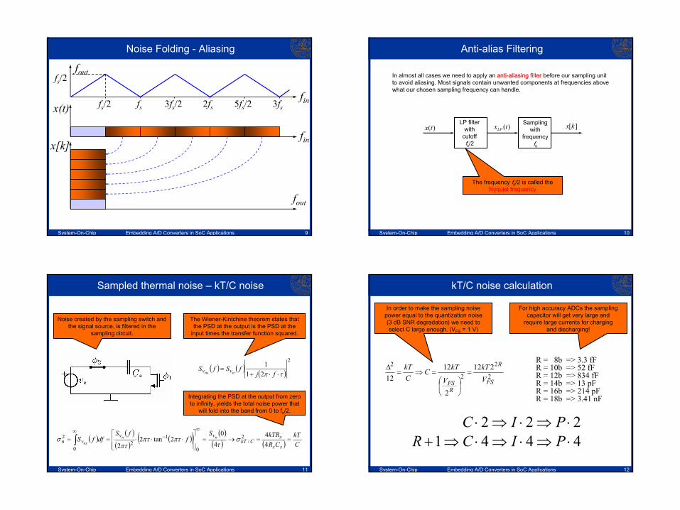
Noise Folding - Aliasing
fin
fout
fs/2 fs 3fs/2 2fs 5fs/2 3fs
fs/2
fin
x(t)
fout
x[k]
System-On-Chip Embedding A/D Converters in SoC Applications 10
Anti-alias Filtering
In almost all cases we need to apply an anti-aliasing filter before our sampling unitto avoid aliasing. Most signals contain unwanted components at frequencies abovewhat our chosen sampling frequency can handle.
LP filterwith
cutofffs/2
Samplingwith
frequencyfs
)(tx )(txLP ][kx
The frequency fs/2 is called the Nyquist frequency
System-On-Chip Embedding A/D Converters in SoC Applications
11
Sampled thermal noise – kT/C noise
( ) ( ) ( )
2
211
τπ ⋅⋅+=
fjfSfS
nns vv
Noise created by the sampling switch and the signal source, is filtered in the
sampling circuit.
The Wiener-Kintchine theorem states that the PSD at the output is the PSD at the
input times the transfer function squared.
Integrating the PSD at the output from zero to infinity, yields the total noise power that
will fold into the band from 0 to fs/2.
( )( )
( )( )( ) ( )
( ) ( ) CkT
CRkTRS
ffS
dffSss
sCkT
vvvn
nnny
==→=
⋅⋅⋅==
∞∞−∫ 4
44
02tan2
22
/00
12
2 στ
πτπτπτ
σ
System-On-Chip Embedding A/D Converters in SoC Applications 12
kT/C noise calculation
2
2
2
2 212
2
1212 FS
R
RFS V
kT
V
kTCCkT
=
=⇒=
∆
In order to make the sampling noise power equal to the quantization noise (3 dB SNR degradation) we need to select C large enough. (VFS = 1 V)
For high accuracy ADCs the sampling capacitor will get very large and
require large currents for charging and discharging!
R = 8b => 3.3 fFR = 10b => 52 fFR = 12b => 834 fFR = 14b => 13 pFR = 16b => 214 pFR = 18b => 3.41 nF
222 ⋅⇒⋅⇒⋅ PIC4441 ⋅⇒⋅⇒⋅⇒+ PICR
System-On-Chip Embedding A/D Converters in SoC Applications

13
Sampling-time jitter
• Any clock signal is affected by jitter (noise on the “zero crossings”)
• Large errors with steep signal slopes
System-On-Chip Embedding A/D Converters in SoC Applications 14
Sampling error caused by jitter
For a sine wave , the jitter-induced error is ( ) ( )sinin inx t A tω= ( )x nT∆
( ) ( ) ( )cosin inx nT A nT nTω δ ω∆ =
Assume that is the sampling of a random variable ; we obtain:
( )nTδ ( )ji tδ
( ) ( ) ( ) ( )2 2
22 2 2cos2in
ji in inAx t A nT nT nTωω ω δ δ = =
The jitter-limited SNR is therefore:
( )( )10log 20log inSSNR nTN
ω δ= = −
Jitter may be the limiting factor in data conversion: if SNR=90dB and fin=100MHz, then the clock jitter must be below 50fs
REMARK: If the SNR does not change with
signal amplitude SUSPECT CLOCK
JITTER !
System-On-Chip Embedding A/D Converters in SoC Applications
15
Maximum jitter vs. input frequency and SNR
SNR
System-On-Chip Embedding A/D Converters in SoC Applications 16
Clock Jitter - Random and Systematic
Second order harmonics likely to appear already for
quite modest signal-to-clock crosstalk !
System-On-Chip Embedding A/D Converters in SoC Applications

17
Clock Jitter Summary
• Not dependent on sampling rate
• SNR due to other distortion is normally dependent on signal amplitude, the jitter limited SNR is not.
• Systematic clock skew creates distortion, random variations in sampling instant generates noise.
• Strong dependence on input frequency (be careful when using low IF conversion)
• Jitter performance can often be improved by careful design
System-On-Chip Embedding A/D Converters in SoC Applications 18
Amplitude quantization - quantization error
( )
max min
12 2
# of quantization levels
in Q
in
Q
FS
FS
Y X
n X n
XM
X X XM
ε
ε
= +
∆ < < + ∆
−∆ ≤ ≤ ∆
∆ =
= −=
The quantization error is a form of data corruption fundamentally unavoidable in data conversion (unless N is infinite)
2# of bits
NMN
==
System-On-Chip Embedding A/D Converters in SoC Applications
19
Quantization error – Ramp input
System-On-Chip Embedding A/D Converters in SoC Applications
This is NOTa random signal !
20
Quantization error – Sinusoidal input
System-On-Chip Embedding A/D Converters in SoC Applications
This is also not a random signal.
Quantization errors are functions of the
input signal !
21
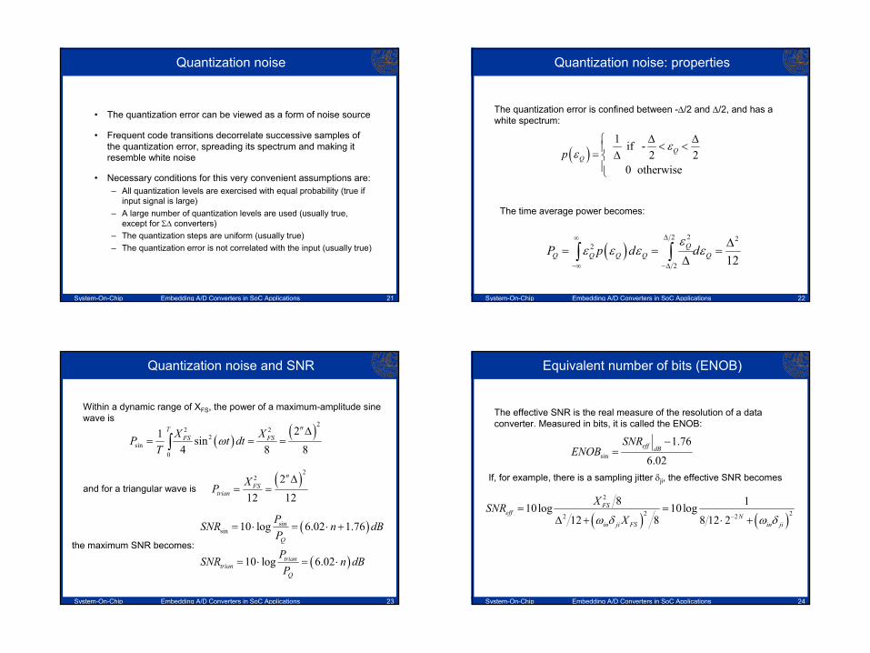
Quantization noise
• The quantization error can be viewed as a form of noise source
• Frequent code transitions decorrelate successive samples of the quantization error, spreading its spectrum and making it resemble white noise
• Necessary conditions for this very convenient assumptions are:– All quantization levels are exercised with equal probability (true if
input signal is large)– A large number of quantization levels are used (usually true,
except for Σ∆ converters)– The quantization steps are uniform (usually true)– The quantization error is not correlated with the input (usually true)
System-On-Chip Embedding A/D Converters in SoC Applications 22
Quantization noise: properties
The quantization error is confined between -∆/2 and ∆/2, and has a white spectrum:
( )1 if -
2 20 otherwise
QQp
εε
∆ ∆ < <= ∆
The time average power becomes:
( )22 2
2
2 12Q
Q Q Q Q QP p d dε
ε ε ε ε∆∞
−∞ −∆
∆= = =
∆∫ ∫
System-On-Chip Embedding A/D Converters in SoC Applications
23
Quantization noise and SNR
Within a dynamic range of XFS, the power of a maximum-amplitude sine wave is
and for a triangular wave is
( ) ( )22 2
2sin
0
21 sin4 8 8
nTFS FSX XP t dt
Tω
∆= = =∫
( )22 2
12 12
nFS
trianXP
∆= =
( )
( )
sinsin 10 log 6.02 1.76
10 log 6.02
Q
triantrian
Q
PSNR n dBP
PSNR n dBP
= ⋅ = ⋅ +
= ⋅ = ⋅the maximum SNR becomes:
System-On-Chip Embedding A/D Converters in SoC Applications 24
Equivalent number of bits (ENOB)
The effective SNR is the real measure of the resolution of a data converter. Measured in bits, it is called the ENOB:
sin
1.76
6.02eff dB
SNRENOB
−=
If, for example, there is a sampling jitter δji, the effective SNR becomes
( ) ( )2
2 22 2
8 110log 10log12 8 8 12 2
FSeff N
in ji FS in ji
XSNRXω δ ω δ−
= =∆ + ⋅ +
System-On-Chip Embedding A/D Converters in SoC Applications

25
Mixed Signal Noise and Distortion (1)
Input to reference crosstalk
Analog input Digital output
Reference signal
Clock signalRout
ref
in Dvv
2=
REMARK: The quality of all input signals are of great importance
for the quality of the output
DC/LF/IF
RF
DCDC
VDD
DC/LF/IF/RFADC
I/O crosstalk
Input to clock crosstalk
Pow
er s
uupl
y in
duce
d jit
ter
System-On-Chip Embedding A/D Converters in SoC Applications 26
Mixed signal Noise and Distortion (2) – Jitter Again!!
10 % power supply variation ~ 10 % timing
edge variation
Use separate power connections for both
digital and analog clocks
Carefully decouple sampling clock
circuits!
System-On-Chip Embedding A/D Converters in SoC Applications
27
Mixed Signal Noise and Distortion (3) - Crosstalk
Clean analog supply for inverters driving switches to avoid
digital power supply noise coupling to
sensitive analog nodes
System-On-Chip Embedding A/D Converters in SoC Applications 28
MS Noise and Distortion (4) – Output signal scrambling
XOR
XOR
XOR
XOR
PRBS
D0
D1
D2
D3
Scrambled data
Systematic output signal
Pseudo random binary sequence with long repetition interval
By scrambling the digital output, the
input/output correlation can be removed.
System-On-Chip Embedding A/D Converters in SoC Applications

29
MS Noise and Distortion (5) – Bondwire inductance
Number (multiple pads for supplies and DCs) and orientation of currents
Increased number of bond wires =
lower inductance = less ringing !
Putting VDD and GND on every second pad decreases the effective inductance by
as much as 30 %
VDD
GND
VDD
GND
Iin
Iout
Iin
Iout
System-On-Chip Embedding A/D Converters in SoC Applications 30
MS Noise and Distortion (6) – Careful Floorplanning
Floorplanning and pad frame
planning
Sensitive analog
Mixedanalogand
digital
Noisydigital
Digital outputs
Quietdigital
Quietdigital
Analog reference
Analog input
Analog supply and
bias
Clock input
Unsensitive analog
System-On-Chip Embedding A/D Converters in SoC Applications
31
MS Noise and Distortion (7) – Differential signals
Differential signalVin = Vin,p-Vin,n
In a well balanced design, disturbances
are sensed as common mode variations and
therefore rejected
System-On-Chip Embedding A/D Converters in SoC Applications
Common modeVcm = (Vin,p+Vin,n)/2
32
Mitigating Mixed Signal Noise and Distortion -Summary
System-On-Chip Embedding A/D Converters in SoC Applications
• Differential signals
• Multiple bondwires
• Careful floorplanning
• Symmetric layout of differential signals
• Decoupling, decoupling, decoupling ...

33
Speed – Accuracy of ADCs
15
10
20
5
1k 10k 100k 1M 10M 100M 1G
INTE
GRAT
ING
DELTA SIGMACONVERTERS
SUCCESSIVE APPROXIMATIONALGORITHMIC
FLASH, TWO-STEPFOLDING, INTERPOLATING
PIPELINEDTIME INTERLEAVING
R
fS
1 level / Tclk
1 word / (OSR Tclk)
1 bit / Tclk
1 word / Tclk
System-On-Chip Embedding A/D Converters in SoC Applications 34
CMOS Scaling Aspects - Opportunities
15
10
20
5
1k 10k 100k 1M 10M 100M 1G
INTE
GRAT
ING
DELTA SIGMACONVERTERS
SUCCESSIVE APPROXIMATIONALGORITHMIC
FLASH, TWO-STEPFOLDING, INTERPOLATING
PIPELINEDTIME INTERLEAVING
R
fS
Increased fT
Digitalcalibration
System-On-Chip Embedding A/D Converters in SoC Applications
35
CMOS Scaling Aspects - Challenges
• Reduced supply voltage -> Reduced signal swings
• Reduced intrinsic gain -> More complex feedback amplifiers
• Poor linearity due to short-channel effects
• Complex switch implementations
System-On-Chip Embedding A/D Converters in SoC Applications 36
Summary and Conclusions
System-On-Chip Embedding A/D Converters in SoC Applications
• Sampling fundamentally limits the bandwidth of ADCs.• Amplitude quantization limits the resolution.
• The sampling circuit accuracy is limited by kT/C thermal noise at low input frequencies and by clock jitter at high frequencies.
• The sampling circuit is very sensitive to mixed signal noise anddistortion.
• Increased speed of deep submicron CMOS enables faster A/D conveters and digital error correction methods that may improve accuracy and power consumption where matching is the limit.
• Low supply voltage is bad for analog design and leads to SNR reduction, reduced DC gain and linearity problems, or increased power consumption....

37
Next lecture – Noise shaping ADCs
How to achieve 80 dB SNR from a 1 bit quantizer....
How to increase the SNR exponentially by increasing the clock rate....
System-On-Chip Embedding A/D Converters in SoC Applications


![International Journal of Innovative Research in Advanced ... · PDF fileMaternal ECG signal generated for mothers heart assuming a 4000 Hz sampling rate[6]. ... M. R. Spiegel, Theory](https://static.fdocuments.us/doc/165x107/5aa31bf37f8b9a436d8dcd30/international-journal-of-innovative-research-in-advanced-ecg-signal-generated.jpg)


