FUNCTIONAL BLOCK DIAGRAM - Digi-Key Sheets/IDT/IDT72V3686,96,106.pdf · 2 commercial temperature...
39
IDT72V3686 IDT72V3696 IDT72V36106 3.3 VOLT CMOS TRIPLE BUS SyncFIFO TM WITH BUS-MATCHING 16,384 x 36 x 2 32,768 x 36 x 2 65,536 x 36 x 2 1 2009 Integrated Device Technology, Inc. All rights reserved. Product specifications subject to change without notice. © IDT and the IDT logo are registered trademarks of Integrated Device Technology, Inc. The SyncFIFO™ is a trademark of Integrated Device Technology, nc. COMMERICAL TEMPERATURE RANGE FEBRUARY 2009 DSC-4676/7 FUNCTIONAL BLOCK DIAGRAM FEATURES • Memory storage capacity: IDT72V3686 – 16,384 x 36 x 2 IDT72V3696 – 32,768 x 36 x 2 IDT72V36106 – 65,536 x 36 x 2 • Clock frequencies up to 100 MHz (6.5ns access time) • Two independent FIFOs buffer data between one bidirectional 36-bit port and two unidirectional 18-bit ports (Port C receives and Port B transmits) • 18-bit (word) and 9-bit (byte) bus sizing of 18 bits (word) on Ports B and C • Select IDT Standard timing (using EFA , EFB , FFA , and FFC flag functions) or First Word Fall Through Timing (using ORA, ORB, IRA, and IRC flag functions) • Programmable Almost-Empty and Almost-Full flags; each has five default offsets (8, 16, 64, 256 and 1024) • Serial or parallel programming of partial flags • Big- or Little-Endian format for word and byte bus sizes • Loopback mode on Port A • Retransmit Capability • Master Reset clears data and configures FIFO, Partial Reset clears data but retains configuration settings • Mailbox bypass registers for each FIFO • Free-running CLKA, CLKB and CLKC may be asynchronous or coincident (simultaneous reading and writing of data on a single clock edge is permitted) • Auto power down minimizes power dissipation • Available in a space-saving 128-pin Thin Quad Flatpack (TQFP) • Pin compatible to the lower density parts, IDT72V3626/72V3636/ 72V3646/72V3656/72V3666/72V3676 • Industrial temperature range (–40°C to +85°C) is available • Green parts available, see ordering information Mail 1 Register Programmable Flag Offset Registers Input Register RAM ARRAY 16,384 x 36 32,768 x 36 65,536 x 36 Write Pointer Read Pointer Status Flag Logic Input Register Output Register RAM ARRAY 16,384 x 36 32,768 x 36 65,536 x 36 Write Pointer Read Pointer Status Flag Logic CLKA CSA W/ RA ENA MBA LOOP Port-A Control Logic FIFO1, Mail1 Reset Logic MRS1 Mail 2 Register MBF2 WENC Port-C Control Logic FIFO2, Mail2 Reset Logic MRS2 MBF1 FIFO1 FIFO2 16 EFB/ORB AEB 18 18 FFC/IRC AFC B0-B17 FFA/IRA AFA FS2 FS0/SD FS1/SEN A0-A35 EFA/ORA AEA 4676 drw01 36 36 Output Bus- Matching Output Register PRS2 PRS1 Timing Mode FWFT C0-C17 CLKB RENB CSB MBB Port-B Control Logic Common Port Control Logic (B and C) BE SIZEB SIZEC CLKC MBC 36 36 36 36 Input Bus- Matching FIFO1 and FIFO2 Retransmit Logic RT1 RT2 RTM
Transcript of FUNCTIONAL BLOCK DIAGRAM - Digi-Key Sheets/IDT/IDT72V3686,96,106.pdf · 2 commercial temperature...

IDT72V3686IDT72V3696
IDT72V36106
3.3 VOLT CMOS TRIPLE BUS SyncFIFOTM WITH BUS-MATCHING
16,384 x 36 x 232,768 x 36 x 265,536 x 36 x 2
12009 Integrated Device Technology, Inc. All rights reserved. Product specifications subject to change without notice.©
IDT and the IDT logo are registered trademarks of Integrated Device Technology, Inc. The SyncFIFO™ is a trademark of Integrated Device Technology, nc.
COMMERICAL TEMPERATURE RANGE FEBRUARY 2009
DSC-4676/7
FUNCTIONAL BLOCK DIAGRAM
FEATURES••••• Memory storage capacity:
IDT72V3686 – 16,384 x 36 x 2IDT72V3696 – 32,768 x 36 x 2IDT72V36106 – 65,536 x 36 x 2
••••• Clock frequencies up to 100 MHz (6.5ns access time)••••• Two independent FIFOs buffer data between one bidirectional
36-bit port and two unidirectional 18-bit ports (Port C receivesand Port B transmits)
••••• 18-bit (word) and 9-bit (byte) bus sizing of 18 bits (word) onPorts B and C
••••• Select IDT Standard timing (using EFA , EFB , FFA , and FFC flagfunctions) or First Word Fall Through Timing (using ORA, ORB,IRA, and IRC flag functions)
••••• Programmable Almost-Empty and Almost-Full flags; each hasfive default offsets (8, 16, 64, 256 and 1024)
••••• Serial or parallel programming of partial flags••••• Big- or Little-Endian format for word and byte bus sizes••••• Loopback mode on Port A••••• Retransmit Capability••••• Master Reset clears data and configures FIFO, Partial Reset
clears data but retains configuration settings••••• Mailbox bypass registers for each FIFO••••• Free-running CLKA, CLKB and CLKC may be asynchronous or
coincident (simultaneous reading and writing of data on a singleclock edge is permitted)
••••• Auto power down minimizes power dissipation••••• Available in a space-saving 128-pin Thin Quad Flatpack (TQFP)••••• Pin compatible to the lower density parts, IDT72V3626/72V3636/
72V3646/72V3656/72V3666/72V3676••••• Industrial temperature range (–40°°°°°C to +85°°°°°C) is available••••• Green parts available, see ordering information
Mail 1Register
Programmable FlagOffset Registers
Inpu
tR
egis
ter
RAM ARRAY16,384 x 3632,768 x 3665,536 x 36
WritePointer
ReadPointer
Status FlagLogic
Inpu
tR
egis
ter
Out
put
Reg
iste
r RAM ARRAY16,384 x 3632,768 x 3665,536 x 36
WritePointer
ReadPointer
Status FlagLogic
CLKACSA
W/RAENA
MBALOOP
Port-AControlLogic
FIFO1,Mail1ResetLogic
MRS1
Mail 2Register
MBF2
WENCPort-CControlLogic
FIFO2,Mail2ResetLogic
MRS2
MBF1
FIFO1
FIFO216
EFB/ORBAEB
18
18
FFC/IRCAFC
B0-B17
FFA/IRAAFA
FS2FS0/SD
FS1/SENA0-A35
EFA/ORAAEA
4676 drw01
36
36
Out
put B
us-
Mat
chin
g
Out
put
Reg
iste
r
PRS2
PRS1
TimingMode
FWFT
C0-C17
CLKBRENBCSBMBB
Port-BControlLogic
CommonPort
ControlLogic
(B and C)
BE
SIZEB
SIZEC
CLKC
MBC
36 36
36 36
Inpu
t Bus
-M
atch
ing
FIFO1 andFIFO2RetransmitLogic
RT1
RT2
RTM

2
COMMERCIAL TEMPERATURE RANGEIDT72V3686/72V3696/72V36106 3.3V CMOS TRIPLE BUS SyncFIFOTM
WITH BUS-MATCHING 16,384 x 36 x 2, 32,768 x 36 x 2, 65, 536 x 36
(Port A) and two unidirectional 18-bit buses (Port B transmits data, Port Creceives data.) FIFO data can be read out of Port B and written into Port C usingeither 18-bit or 9-bit formats with a choice of Big- or Little-Endian configurations.
These devices are a synchronous (clocked) FIFO, meaning each portemploys a synchronous interface. All data transfers through a port are gatedto the LOW-to-HIGH transition of a port clock by enable signals. The clocks foreach port are independent of one another and can be asynchronous or
DESCRIPTIONThe IDT72V3686/72V3696/72V36106 are designed to run off a 3.3V supply
for exceptionally low-power consumption. These devices are a monolithic,high-speed, low-power, CMOS Triple Bus synchronous (clocked) FIFOmemory which supports clock frequencies up to 100 MHz and has read accesstimes as fast as 6.5ns. Two independent 16,384/32,768/65,536 x 36 dual-portSRAM FIFOs on board each chip buffer data between a bidirectional 36-bit bus
PIN CONFIGURATION
TQFP (PK128-1, order code: PF)TOP VIEW
W/RA CLKB
4676 drw02
1234567891011121314151617181920212223242526272829303132333435363738
ENA CLKA
GND A35 A34 A33 A32
VccA31
A30 GND
A29 A28 A27 A26 A25A24A23
BE/FWFTGNDA22Vcc
A21A20 A19A18
GND A17
A16A15A14A13VccA12
GNDA11A10
39 40 41 42 43 44 45 46 47 48 49 50 51 52 53 54 55 56 57 58 59 60 61 62 63 64
6566676869707172737475767778798081828384858687888990919293949596979899
100
102101
128
127
126
125
124
123
122
121
120
119
118
117
116
115
114
113
112
111
110
109
108
107
106
105
PRS2/RT2
C17C16C15C14
MBCRTM
C13C12C11C10C9C8
C7C6SIZEBGNDC5C4C3C2C1C0GNDB17B16
B15B14B13B12GNDB11B10
CS
AF
FA
/IRA
EF
A/O
RA
PR
S1/
RT
1
AF
AA
EA
MB
F2
MB
AM
RS
1
FS
0/S
DC
LKC
GN
DF
S1/
SE
NM
RS
2M
BB
MB
F1
AE
BA
FC
EF
B/O
RB
FF
C/IR
CG
ND
CS
BW
EN
CR
EN
B
A9
A8
A7
A
6
GN
D
A5
A4
A3
A2 A1
A0
GN
D B0
B1
B2
B3
B4
B
5 G
ND
B
6
B7
B
9
104
103
INDEX
SIZEC
B8
VCC
VCCV
CC
VC
C
VC
C
VC
C
LOOP
FS
2
3
COMMERCIAL TEMPERATURE RANGEIDT72V3686/72V3696/72V36106 3.3V CMOS TRIPLE BUS SyncFIFOTM
WITH BUS-MATCHING 16,384 x 36 x 2, 32,768 x 36 x 2, 65, 536 x 36
coincident. The enables for each port are arranged to provide a simplebidirectional interface between microprocessors and/or buses with synchro-nous control.
Communication between each port may bypass the FIFOs via two mailboxregisters. The mailbox registers' width matches the selected bus width of portsB and C. Each mailbox register has a flag (MBF1 and MBF2) to signal whennew mail has been stored.
Two kinds of reset are available on these FIFOs: Master Reset and PartialReset. Master Reset initializes the read and write pointers to the first locationof the memory array and selects serial flag programming, parallel flag program-ming, or one of five possible default flag offset settings, 8, 16, 64, 256 or 1,024.Each FIFO has its own, independent Master Reset pin, MRS1 and MRS2.
Partial Reset also sets the read and write pointers to the first location of thememory. Unlike Master Reset, any settings existing prior to Partial Reset (i.e.,programming method and partial flag default offsets) are retained. Partial Resetis useful since it permits flushing of the FIFO memory without changing anyconfiguration settings. Each FIFO has its own, independent Partial Reset pin,PRS1 and PRS2. Note that the Retransmit Mode, RTM pin must be LOW at thepoint a partial reset is performed.
Both FIFO's have Retramsmit capability, when a Retransmit is performed ona respective FIFO only the read pointer is reset to the first memory location. ARetransmit is performed by using the Retransmit Mode, RTM pin in conjunctionwith the Retransmit pins RT1 or RT2, for each respective FIFO. Note that thetwo Retransmit pins RT1 and RT2 are muxed with the Partial Reset pins.
These devices have two modes of operation: In the IDT Standard mode, thefirst word written to an empty FIFO is deposited into the memory array. A readoperation is required to access that word (along with all other words residingin memory). In the First Word Fall Through mode (FWFT), the first word writtento an empty FIFO appears automatically on the outputs, no read operationrequired (Nevertheless, accessing subsequent words does necessitate aformal read request). The state of the BE/FWFT pin during Master Resetdetermines the mode in use.
Each FIFO has a combined Empty/Output Ready Flag (EFA/ORA and EFB/ORB) and a combined Full/Input Ready Flag (FFA/IRA and FFC/IRC). TheEF and FF functions are selected in the IDT Standard mode. EF indicateswhether or not the FIFO memory is empty. FF shows whether the memory isfull or not. The IR and OR functions are selected in the First Word Fall Throughmode. IR indicates whether or not the FIFO has available memory locations.OR shows whether the FIFO has data available for reading or not. It marks thepresence of valid data on the outputs.
Each FIFO has a programmable Almost-Empty flag (AEA and AEB) and aprogrammable Almost-Full flag (AFA and AFC). AEA and AEB indicate when
a selected number of words remain in the FIFO memory. AFA and AFC indicatewhen the FIFO contains more than a selected number of words.
FFA/IRA, FFC/IRC, AFA and AFC are two-stage synchronized to the PortClock that writes data into its array. EFA/ORA, EFB/ORB, AEA, and AEB aretwo-stage synchronized to the Port Clock that reads data from its array.Programmable offsets for AEA, AEB, AFA, AFC are loaded in parallel usingPort A or in serial via the SD input. Five default offset settings are also provided.The AEA and AEB threshold can be set at 8, 16, 64, 256, and 1,024 locationsfrom the empty boundary and the AFA and AFC threshold can be set at 8, 16,64, 256 or 1,024 locations from the full boundary. All these choices are madeusing the FS0, FS1 and FS2 inputs during Master Reset.
Interspersed Parity can also be selected during a Master Reset of the FIFO.If Interspersed Parity is selected then during parallel programming of the flagoffset values, the device will ignore data line A8. If Non-Interspersed Parity isselected then data line A8 will become a valid bit.
A Loopback function is provided on Port A. When the Loop feature is selectedvia the LOOP pin, the data output from FIFO2 will be directed to the data inputof FIFO1. If Loop is selected and Port A is set-up for write operation via W/RApin, then data output from FIFO2 will be written to FIFO1, but will not be placedon the output Port A (A0-A35). If Port A is set-up for read operation via W/RAthen data output from FIFO2 will be written into FIFO1 and placed onto Port A(A0-A35). The Loop will continue to happen provided that FIFO1 is not full andFIFO2 is not empty. If during a Loop sequence FIFO1 becomes full then anydata that continues to be read out from FIFO2 will only be placed on the PortA (A0-A35) lines, provided that Port A is set-up for read operation. If during aLoop sequence the FIFO2 becomes empty, then the last word from FIFO2 willcontinue to be clocked into FIFO1 until FIFO1 becomes full or until the Loopfunction is stopped. The Loop feature can be useful when performing systemdebugging and remote loopbacks.
Two or more FIFOs may be used in parallel to create wider data paths. Sucha width expansion requires no additional, external components. Furthermore,two IDT72V3686/72V3696/72V36106 FIFOs can be combined with unidirec-tional FIFOs capable of First Word Fall Through timing (i.e. the SuperSync FIFOfamily) to form a depth expansion.
If, at any time, the FIFO is not actively performing a function, the chip willautomatically power down. During the power down state, supply currentconsumption (ICC) is at a minimum. Initiating any operation (by activating controlinputs) will immediately take the device out of the power down state.
The IDT72V3686/72V3696/72V36106 are characterized for operation from0°C to 70°C. Industrial temperature range (-40°C to +85°C) is available byspecial order. They are fabricated using IDT’s high speed, submicron CMOStechnology.

4
COMMERCIAL TEMPERATURE RANGEIDT72V3686/72V3696/72V36106 3.3V CMOS TRIPLE BUS SyncFIFOTM
WITH BUS-MATCHING 16,384 x 36 x 2, 32,768 x 36 x 2, 65, 536 x 36
PIN DESCRIPTIONSSymbol Name I/O Description
A0-A35 Port A Data I/O 36-bit bidirectional data port for side A.
AEA Port A Almost- O Programmable Almost-Empty flag synchronized to CLKA. It is LOW when the number of words in FIFO2Empty Flag is less than or equal to the value in the Almost-Empty A Offset register, X2.
AEB Port B Almost- O Programmable Almost-Empty flag synchronized to CLKB. It is LOW when the number of words in FIFO1Empty Flag is less than or equal to the value in the Almost-Empty B Offset register, X1.
AFA Port A Almost- O Programmable Almost-Full flag synchronized to CLKA. It is LOW when the number of empty locationsFull Flag in FIFO1 is less than or equal to the value in the Almost-Full A Offset register, Y1.
AFC Port C Almost- O Programmable Almost-Full flag synchronized to CLKC. It is LOW when the number of empty locationsFull Flag in FIFO2 is less than or equal to the value in the Almost-Full C Offset register, Y2.
B0-B17 Port B Data O 18-bit output data port for side B.
BE/FWFT Big-Endian/ I This is a dual purpose pin. During Master Reset, a HIGH on BE will select Big-Endian operation.First Word Fall In this case, depending on the bus size, the most significant byte or word on Port A is read fromThrough Select Port B first (A-to-B data flow) or is written to Port C first (C-to-A data flow). A LOW on BE will select
Little-Endian operation. In this case, the least significant byte or word on Port A is read from Port B first(A-to-B data flow) or is written to Port C first (C-to-A data flow).
After Master Reset, this pin selects the timing mode. A HIGH on FWFT selects IDT Standard mode, aLOW selects First Word Fall Through mode. Once the timing mode has been selected, the level onFWFT must be static throughout device operation.
C0-C17 Port C Data I 18-bit input data port for side C.
CLKA Port A Clock I CLKA is a continuous clock that synchronizes all data transfers through Port A and can beasynchronous or coincident to CLKB. FFA/IRA, EFA/ORA, AFA, and AEA are all synchronized tothe LOW-to-HIGH transition of CLKA.
CLKB Port B Clock I CLKB is a continuous clock that synchronizes all data transfers through Port B and can be asynchronousor coincident to CLKA. EFB/ORB and AEB are synchronized to the LOW-to-HIGH transition of CLKB.
CLKC Port C Clock I CLKC is a continuous clock that synchronizes all data transfers through Port C and can be asynchronousor coincident to CLKA. FFC/IRC and AFC are synchronized to the LOW-to-HIGH transition of CLKC.
CSA Port A Chip I CSA must be LOW to enable to LOW-to-HIGH transition of CLKA to read or write on Port A. The A0-A35Select outputs are in the high-impedance state when CSA is HIGH.
CSB Port B Chip I CSB must be LOW to enable a LOW-to-HIGH transition of CLKB to read data on Port B. The B0-B17Select outputs are in the high-impedance state when CSB is HIGH.
EFA/ORA Port A Empty/ O This is a dual function pin. In the IDT Standard mode, the EFA function is selected. EFA indicatesOutput Ready whether or not the FIFO2 memory is empty. In the FWFT mode, the ORA function is selected. ORAFlag indicates the presence of valid data on the A0-A35 outputs, available for reading. EFA/ORA is
synchronized to the LOW-to-HIGH transition of CLKA.
EFB/ORB Port B Empty/ O This is a dual function pin. In the IDT Standard mode, the EFB function is selected. EFB indicatesOutput Ready Flag whether or not the FIFO1 memory is empty. In the FWFT mode, the ORB function is selected. ORB
indicates the presence of valid data on the B0-B17 outputs, available for reading. EFB/ORB is synchronizedto the LOW-to-HIGH transition of CLKB.
ENA Port A Enable I ENA must be HIGH to enable a LOW-to-HIGH transition of CLKA to read or write data on Port A.
FFA/IRA Port A Full/ O This is a dual function pin. In the IDT Standard mode, the FFA function is selected. FFA indicatesInput Ready Flag whether or not the FIFO1 memory is full. In the FWFT mode, the IRA function is selected. IRA
indicates whether or not there is space available for writing to the FIFO1 memory. FFA/IRA issynchronized to the LOW-to-HIGH transition of CLKA.
FFC/IRC Port C Full/ O This is a dual function pin. In the IDT Standard mode, the FFC function is selected. FFC indicatesInput Ready Flag whether or not the FIFO2 memory is full. In the FWFT mode, the IRC function is selected. IRC
indicates whether or not there is space available for writing to the FIFO2 memory. FFC/IRC issynchronized to the LOW-to-HIGH transition of CLKC.

5
COMMERCIAL TEMPERATURE RANGEIDT72V3686/72V3696/72V36106 3.3V CMOS TRIPLE BUS SyncFIFOTM
WITH BUS-MATCHING 16,384 x 36 x 2, 32,768 x 36 x 2, 65, 536 x 36
PIN DESCRIPTIONS (CONTINUED)Symbol Name I/O Description
FS0/SD Flag Offset Select 0/ I FS1/SEN and FS0/SD are dual-purpose inputs used for flag Offset register programming. During Master Reset,Serial Data FS1/SEN and FS0/SD, together with FS2, select the flag offset programming method. Three Offset register
programming methods are available: automatically load one of five preset values (8, 16, 64, 256 or 1,024),FS1/SEN Flag Offset Select 1/ I parallel load from Port A, and serial load.
Serial EnableWhen serial load is selected for flag Offset register programming, FS1/SEN is used as an enable synchronous to
FS2(1) Flag Offset Select 2 I the LOW-to-HIGH transition of CLKA. When FS1/SEN is LOW, a rising edge on CLKA load the bit present onFS0/SD into the X and Y registers. The number of bit writes required to program the Offset registers is 56 for the72V3686, 60 for the 72V3696, and 64 for the 72V36106. The first bit write stores the Y-register (Y1) MSB andthe last bit write stores the X-register (X2) LSB.
LOOP Loopback Select I This pin selects the loopback feature for Port A. During Loopback data from FIFO2 will be directed to the input ofFIFO1. to initiate a Loop the LOOP pin must be held LOW and the ENA pin must be HIGH.
MBA Port A Mailbox I A HIGH level on MBA chooses a mailbox register for a Port A read or write operation. When the A0-A35Select outputs are active, a HIGH level on MBA selects data from the mail2 register for output and a LOW level selects
FIFO2 output-register data for output.
MBB Port B Mailbox I A HIGH level on MBB chooses a mailbox register for a Port B read operation. When the B0-B17 outputs areSelect active, a HIGH level on MBB selects data from the mail1 register for output and a LOW level selects FIFO1 output
register data for output.
MBC Port C Mailbox I A HIGH level on MBC chooses the mail2 register for a Port C write operation. This pin must be HIGH duringSelect Master Reset.
MBF1 Mail1 Register O MBF1 is set LOW by a LOW-to-HIGH transition of CLKA that writes data to the mail1 register. Writes to the mail1Flag register are inhibited while MBF1 is LOW. MBF1 is set HIGH by a LOW-to-HIGH transition of CLKB when a
Port B read is selected and MBB is HIGH. MBF1 is set HIGH following either a Master or Partial Reset of FIFO1.
MBF2 Mail2 Register O MBF2 is set LOW by a LOW-to-HIGH transition of CLKC that writes data to the mail2 register. Writes to the mail2Flag register are inhibited while MBF2 is LOW. MBF2 is set HIGH by a LOW-to-HIGH transition of CLKA when a
Port A read is selected and MBA is HIGH. MBF2 is set HIGH following either a Master or Partial Reset of FIFO2.
MRS1 Master Reset I A LOW on this pin initializes the FIFO1 read and write pointers to the first location of memory and sets the Port Boutput register to all zeroes. A LOW-to-HIGH transition on MRS1 selects the programming method (serial orparallel) and one of five programmable flag default offsets for FIFO1 and FIFO2. It also configures ports B andC for bus size and endian arrangement. Four LOW-to-HIGH transitions of CLKA and four LOW-to-HIGHtransitions of CLKB must occur while MRS1 is LOW.
MRS2 Master Reset I A LOW on this pin initializes the FIFO2 read and write pointers to the first location of memory and sets the Port Aoutput register to all zeroes. A LOW-to-HIGH transition on MRS2, toggled simultaneously with MRS1, selectsthe programming method (serial or parallel) and one of the five flag default offsets for FIFO2. Four LOW-to-HIGHtransitions of CLKA and four LOW-to-HIGH transitions of CLKC must occur while MRS2 is LOW.
PRS1/ Partial Reset/ I This pin is muxed for both Partial Reset and Retransmit operations, it is used in conjunction with the RTM pin. If RTMRT1 Retransmit FIFO1 is in a LOW condition, a LOW on this pin performs a Partial Reset on FIFO1 and initializes the FIFO1 read and write
pointers to the first location of memory and sets the Port B output register to all zeroes. During Partial Reset, the currentlyselected bus size, endian arrangement, programming method (serial or parallel), and programmable flag settings areall retained. If RTM is HIGH, a LOW on this pin performs a Retransmit and initializes the FIFO1 read pointer only tothe first memory location.
PRS2/ Partial Reset/ I This pin is muxed for both Partial Reset and Retransmit operations, it is used in conjunction with the RTM pin. If RTM
RT2 Retransmit FIFO2 is in a LOW condition, a LOW on this pin performs a Partial Reset on FIFO2 and initializes the FIFO2 read and writeselected bus size, endian arrangement, programming method (serial or parallel), and programmable flag settings areall retained. If RTM is HIGH, a LOW on this pin performs a Retransmit and initializes the FIFO2 read pointer only tothe first memory location.
RENB Port B Read Enable I RENB must be HIGH to enable a LOW-to-HIGH transition of CLKB to read data on Port B.
RTM Retransmit Mode I This pin is used in conjunction with the RT1 and RT2 pins. When RTM is HIGH a Retransmit is performed on FIFO1or FIFO2 respectively.
6
COMMERCIAL TEMPERATURE RANGEIDT72V3686/72V3696/72V36106 3.3V CMOS TRIPLE BUS SyncFIFOTM
WITH BUS-MATCHING 16,384 x 36 x 2, 32,768 x 36 x 2, 65, 536 x 36
SIZEB(1) Port B I SIZEB determines the bus width of Port B. A HIGH on this pin selects byte (9-bit) bus size. A LOW on this pinBus Size Select selects word (18-bit) bus size. SIZEB works with SIZEC and BE to select the bus size and endian arrangement
for ports B and C. The level of SIZEB must be static throughout device operation.
SIZEC(1) Port C I SIZEC determines the bus width of Port C. A HIGH on this pin selects byte (9-bit) bus size. A LOW on this pinBus Size Select selects word (18-bit) bus size. SIZEC works with SIZEB and BE to select the bus size and endian arrangement
for ports B and C. The level of SIZEC must be static throughout device operation.
WENC Port C Write Enable I WENC must be HIGH to enable a LOW-to-HIGH transition of CLKC to write data on Port C.
W/RA Port A Write/ I A HIGH selects a write operation and a LOW selects a read operation on Port A for a LOW-to-HIGH transition ofRead Select CLKA. The A0-A35 outputs are in the HIGH impedance state when W/RA is HIGH.
PIN DESCRIPTIONS (CONTINUED) Symbol Name I/O Description
NOTE:1. FS2, SIZEB and SIZEC inputs are not TTL compatible. These inputs should be tied to GND or VCC.

7
COMMERCIAL TEMPERATURE RANGEIDT72V3686/72V3696/72V36106 3.3V CMOS TRIPLE BUS SyncFIFOTM
WITH BUS-MATCHING 16,384 x 36 x 2, 32,768 x 36 x 2, 65, 536 x 36
Symbol Rating Commercial Unit
VCC Supply Voltage Range –0.5 to +4.6 V
VI(2) Input Voltage Range –0.5 to VCC+0.5 V
VO(2) Output Voltage Range –0.5 to VCC+0.5 V
IIK Input Clamp Current (VI < 0 or VI > VCC) ±20 mA
IOK Output Clamp Current (VO = < 0 or VO > VCC) ±50 mA
IOUT Continuous Output Current (VO = 0 to VCC) ±50 mA
ICC Continuous Current Through VCC or GND ±400 mA
TSTG Storage Temperature Range –65 to 150 °C
NOTES:1. Stresses beyond those listed under "Absolute Maximum Ratings" may cause permanent damage to the device. These are stress ratings only and functional operation of the device at these
or any other conditions beyond those indicated under "recommended operating conditions" is not implied. Exposure to absolute-maximum-rated conditions for extended periods may affectdevice reliability.
2. The input and output voltage ratings may be exceeded provided the input and output current ratings are observed.
ABSOLUTE MAXIMUM RATINGS OVER OPERATING FREE-AIRTEMPERATURE RANGE (Unless otherwise noted)(1)
NOTES:1. All typical values are at VCC = 3.3V, TA = 25°C.2. Vcc = 3.3V ± 0.15V, TA = 0° to +70°; JEDEC JESD8-A compliant.3. For additional ICC information, see Figure 1, Typical Characteristics: Supply Current (ICC) vs. Clock Frequency (fS).4. Characterized values, not currently tested.
ELECTRICAL CHARACTERISTICS OVER RECOMMENDED OPERATINGFREE-AIR TEMPERATURE RANGE (Unless otherwise noted)
RECOMMENDED OPERATING CONDITIONS
NOTE:1. Vcc = 3.3V ± 0.15V, JEDEC JESD8-A compliant
Symbol Parameter Min. Typ. Max. Unit
VCC Supply Voltage 3.15 3.3 3.45 V
VIH High-Level Input Voltage 2 — VCC+0.5 V
VIL Low-Level Input Voltage — — 0.8 V
IOH High-Level Output Current — — –4 mA
IOL Low-Level Output Current — — 8 mA
TA Operating Temperature 0 — 70 °C
IDT72V3686IDT72V3696IDT72V36106Commercial
tCLK = 10, 15 ns(2)
Symbol Parameter Test Conditions Min. Typ. Max. UnitVOH Output Logic "1" Voltage VCC = 3.0V, IOH = –4 mA 2.4 — — V
VOL Output Logic "0" Voltage VCC = 3.0V, IOL = 8 mA — — 0.5 V
ILI Input Leakage Current (Any Input) VCC = 3.6V, VI = VCC or 0 — — ±5 µA
ILO Output Leakage Current VCC = 3.6V, VO = VCC or 0 — — ±5 µA
ICC2(3) Standby Current (with CLKA, CLKB and CLKC running) VCC = 3.6V, VI = VCC - 0.2V or 0 — — 15 mA
ICC3(3) Standby Current (no clocks running) VCC = 3.6V, VI = VCC - 0.2V or 0 — — 5 mA
CIN(4) Input Capacitance VI = 0, f = 1 MHz — 4 — pF
COUT(4) Output Capacitance VO = 0, f = 1 MHZ — 8 — pF

8
COMMERCIAL TEMPERATURE RANGEIDT72V3686/72V3696/72V36106 3.3V CMOS TRIPLE BUS SyncFIFOTM
WITH BUS-MATCHING 16,384 x 36 x 2, 32,768 x 36 x 2, 65, 536 x 36
DETERMINING ACTIVE CURRENT CONSUMPTION AND POWER DISSIPATIONThe ICC(f) current for the graph in Figure 1 was taken while simultaneously reading and writing a FIFO on the IDT72V3686/72V3696/72V36106 with CLKA,
CLKB and CLKC set to fS. All data inputs and data outputs change state during each clock cycle to consume the highest supply current. Data outputs weredisconnected to normalize the graph to a zero capacitance load. Once the capacitance load per data-output channel and the number of these device's inputsdriven by TTL HIGH levels are known, the power dissipation can be calculated with the equation below.
CALCULATING POWER DISSIPATIONWith ICC(f) taken from Figure 1, the maximum power dissipation (PT) of these FIFOs may be calculated by:
PT = VCC x ICC(f) + Σ(CL x VCC2 x fo)N
where:N = number of used outputs (36-bit (long word), 18-bit (word) or 9-bit (byte) bus size)CL = output capacitance loadfo = switching frequency of an output
Figure 1. Typical Characteristics: Supply Current (ICC) vs. Clock Frequency (fS)
0 10 20 30 40 50 60 70
0
10
20
30
40
50
60
fS ⎯ Clock Frequency ⎯ MHz
ICC
(f)
Sup
ply
Cur
rent
m
A
fdata = 1/2 fS
TA = 25°C
CL = 0 pF
4676 drw03
70
90
80
100
80 90 100
VCC = 3.3V
VCC = 3.6V
VCC = 3.0V

9
COMMERCIAL TEMPERATURE RANGEIDT72V3686/72V3696/72V36106 3.3V CMOS TRIPLE BUS SyncFIFOTM
WITH BUS-MATCHING 16,384 x 36 x 2, 32,768 x 36 x 2, 65, 536 x 36
TIMING REQUIREMENTS OVER RECOMMENDED RANGES OF SUPPLYVOLTAGE AND OPERATING FREE-AIR TEMPERATURE
IDT72V3686L10 IDT72V3686L15IDT72V3696L10 IDT72V3696L15IDT72V36106L10 IDT72V36106L15
Symbol Parameter Min. Max. Min. Max. Unit
fS Clock Frequency, CLKA, CLKB, or CLKC — 100 — 66.7 MHz
tCLK Clock Cycle Time, CLKA, CLKB, or CLKC 10 — 15 — ns
tCLKH Pulse Duration, CLKA, CLKB, or CLKC HIGH 4.5 — 6 — ns
tCLKL Pulse Duration, CLKA, CLKB, OR CLKC LOW 4.5 — 6 — ns
tDS Setup Time, A0-A35 before CLKA↑ and C0-C17 before CLKC↑ 3 — 4 — ns
tENS1 Setup Time, CSA and W/RA before CLKA↑; CSB 4 — 4.5 — ns before CLKB↑
tENS2 Setup Time, ENA, and MBA before CLKA↑; RENB 3 — 4.5 — nsand MBB before CLKB↑; WENC and MBC before CLKC↑
tRSTS Setup Time, MRS1, MRS2, PRS1, PRS2, RT1 or RT2 5 — 5 — nsLOW before CLKA↑ or CLKB↑(1)
tFSS Setup Time, FS0, FS1, FS2 before MRS1 and MRS2 HIGH 7.5 — 8.5 — ns
tBES Setup Time, BE/FWFT before MRS1 and MRS2 HIGH 7.5 — 7.5 — ns
tSDS Setup Time, FS0/SD before CLKA↑ 3 — 4 — ns
tSENS Setup Time, FS1/SEN before CLKA↑ 3 — 4 — ns
tFWS Setup Time, BE/FWFT before CLKA↑ 0 — 0 — ns
tRTMS Setup Time, RTM before RT1; RTM before RT2 5 — 5 — ns
tDH Hold Time, A0-A35 after CLKA↑ and C0-C17 after CLKC↑ 0.5 — 1 — ns
tENH Hold Time, CSA, W/RA, ENA, and MBA after CLKA↑; CSB, 0.5 — 1 — nsRENB, and MBB after CLKB↑; WENC and MBC after CLKC↑
tRSTH Hold Time, MRS1, MRS2, PRS1, PRS2, RT1 or RT2 4 — 4 — nsLOW after CLKA↑ or CLKB↑ (1)
tFSH Hold Time, FS0, FS1, FS2 after MRS1 and MRS2 HIGH 2 — 2 — ns
tBEH Hold Time, BE/FWFT after MRS1 and MRS2 HIGH 2 — 2 — ns
tSDH Hold Time, FS0/SD after CLKA↑ 0.5 — 1 — ns
tSENH Hold Time, FS1/SEN HIGH after CLKA↑ 0.5 — 1 — ns
tSPH Hold Time, FS1/SEN HIGH after MRS1 and MRS2 HIGH 2 — 2 — ns
tRTMH Hold Time, RTM after RT1; RTM after RT2 5 — 5 — ns
tSKEW1(2) Skew Time, between CLKA↑ and CLKB↑ for EFB/ORB and 5 — 7.5 — nsFFA/IRA; between CLKA↑ and CLKC↑ for EFA/ORA andFFC/IRC
tSKEW2(2,3) Skew Time, between CLKA↑ and CLKB↑ for AEB and AFA; 12 — 12 — nsbetween CLKA↑ and CLKC↑ for AEA and AFC
NOTES:1. Requirement to count the clock edge as one of at least four needed to reset a FIFO.2. Skew time is not a timing constraint for proper device operation and is only included to illustrate the timing relationship among CLKA cycle, CLKB cycle, and CLKC cycle.3. Design simulated, not tested.
(Vcc = 3.3V ± 0.15V; TA = 0ο C to +70ο C; JEDEC JESD8-A compliant)

10
COMMERCIAL TEMPERATURE RANGEIDT72V3686/72V3696/72V36106 3.3V CMOS TRIPLE BUS SyncFIFOTM
WITH BUS-MATCHING 16,384 x 36 x 2, 32,768 x 36 x 2, 65, 536 x 36
SWITCHING CHARACTERISTICS OVER RECOMMENDED RANGES OF SUPPLYVOLTAGE AND OPERATING FREE-AIR TEMPERATURE, CL = 30PF
IDT72V3686L10 IDT72V3686L15IDT72V3696L10 IDT72V3696L15IDT72V36106L10 IDT72V36106L15
Symbol Parameter Min. Max. Min. Max. Unit
tA Access Time, CLKA↑ to A0-A35 and CLKB↑ to B0-B17 2 6.5 2 10 ns
tWFF Propagation Delay Time, CLKA↑ to FFA/IRA and CLKC↑ to 2 6.5 2 8 nsFFC/IRC
tREF Propagation Delay Time, CLKA↑ to EFA/ORA and CLKB↑ to 1 6.5 1 8 nsEFB/ORB
tPAE Propagation Delay Time, CLKA↑ to AEA and CLKB↑ to AEB 1 6.5 1 8 ns
tPAF Propagation Delay Time, CLKA↑ to AFA and CLKC↑ to AFC 1 6.5 1 8 ns
tPMF Propagation Delay Time, CLKA↑ to MBF1 LOW or MBF2 0 6.5 0 8 nsHIGH, CLKB↑ to MBF1 HIGH, and CLKC↑ to MBF2 LOW
tPMR Propagation Delay Time, CLKA↑ to B0-B17(1) and CLKC↑ 2 6.5 2 10 nsto A0-A35(2)
tMDV Propagation Delay Time, MBA to A0-A35 valid and MBB to 2 8 2 10 nsB0-B17 valid
tRSF Propagation Delay Time, MRS1 or PRS1 LOW to AEB 1 10 1 15 nsLOW, AFA HIGH, and MBF1 HIGH and MRS2 or PRS2LOW to AEA LOW, AFC HIGH, and MBF2 HIGH
tEN Enable Time, CSA or W/RA LOW to A0-A35 Active and 2 6 2 10 nsCSB LOW to B0-B17 Active
tDIS Disable Time, CSA or W/RA HIGH to A0-A35 at high 1 6 1 8 nsimpedance and CSB HIGH to B0-B17 at HIGH impedance
NOTES:1. Writing data to the mail1 register when the B0-B17 outputs are active and MBB is HIGH.2. Writing data to the mail2 register when the A0-A35 outputs are active and MBA is HIGH.3. Vcc = 3.3V ± 0.15V; TA = 0° to +70°.
(Vcc = 3.3V ± 0.15V; TA = 0ο C to +70ο C; JEDEC JESD8-A compliant)
11
COMMERCIAL TEMPERATURE RANGEIDT72V3686/72V3696/72V36106 3.3V CMOS TRIPLE BUS SyncFIFOTM
WITH BUS-MATCHING 16,384 x 36 x 2, 32,768 x 36 x 2, 65, 536 x 36
SIGNAL DESCRIPTIONMASTER RESET (MRS1, MRS2)
After power up, a Master Reset operation must be performed by providinga LOW pulse to MRS1 and MRS2 simultaneously. Afterwards, the FIFO1memory of the IDT72V3686/72V3696/72V36106 undergoes a complete resetby taking its associated Master Reset (MRS1) input LOW for at least four PortA Clock (CLKA) and four Port B Clock (CLKB) LOW-to-HIGH transitions. TheFIFO2 memory undergoes a complete reset by taking its associated MasterReset (MRS2) input LOW for at least four Port A Clock (CLKA) and four PortC Clock (CLKC) LOW-to-HIGH transitions. The Master Reset inputs can switchasynchronously to the clocks. A Master Reset initializes the associated read andwrite pointers to the first location of the memory and forces the Full/Input Readyflag (FFA/IRA, FFC/IRC) LOW, the Empty/Output Ready flag (EFA/ORA, EFB/ORB) LOW, the Almost-Empty flag (AEA, AEB) LOW and the Almost-Full flag(AFA, AFC) HIGH. A Master Reset also forces the associated Mailbox Flag(MBF1, MBF2) of the parallel mailbox register HIGH. After a Master Reset, theFIFO's Full/Input Ready flag is set HIGH after two Write Clock cycles. Then theFIFO is ready to be written to.
A LOW-to-HIGH transition on the FIFO1 Master Reset (MRS1) input latchesthe value of the Big-Endian (BE) input for determining the order by which bytesare transferred through Ports B and C. It also latches the values of the Flag Select(FS0, FS1 and FS2) inputs for choosing the Almost-Full and Almost-Emptyoffsets and programming method.
A LOW-to-HIGH transition on the FIFO2 Master Reset (MRS2) clears the flagoffset registers of FIFO2 (X2, Y2). A LOW-to-HIGH transition on the FIFO2Master Reset (MRS2) together with the FIFO1 Master Reset input (MRS1)latches the value of the Big-Endian (BE) input for Ports B and C and also latchesthe values of the Flag Select (FS0, FS1 and FS2) inputs for choosing the Almost-Full and Almost-Empty offsets and programming method (for details see Table1, Flag Programming, and Almost-Empty and Almost-Full flag offset program-ming section). The relevant Master Reset timing diagrams can be found inFigure 4 and 5.
Note that MBC must be HIGH during Master Reset (until FFA/IRA and FFC/IRC go HIGH). MBA and MBB are "don't care" inputs1 during Master Reset.
PARTIAL RESET (PRS1, PRS2)The FIFO1 memory of these devices undergoes a limited reset by taking its
associated Partial Reset (PRS1) input LOW for at least four Port A Clock (CLKA)and four Port B Clock (CLKB) LOW-to-HIGH transitions. The FIFO2 memoryundergoes a limited reset by taking its associated Partial Reset (PRS2) inputLOW for at least four Port A Clock (CLKA) and four Port C Clock (CLKC) LOW-to-HIGH transitions. The RTM pin must be LOW during the time of partial reset.The Partial Reset inputs can switch asynchronously to the clocks. A Partial Resetinitializes the internal read and write pointers and forces the Full/Input Readyflag (FFA/IRA, FFC/IRC) LOW, the Empty/Output Ready flag (EFA/ORA, EFB/ORB) LOW, the Almost-Empty flag (AEA, AEB) LOW, and the Almost-Full flag(AFA, AFC) HIGH. A Partial Reset also forces the Mailbox Flag (MBF1, MBF2)of the parallel mailbox register HIGH. After a Partial Reset, the FIFO’s Full/InputReady flag is set HIGH after two Write Clock cycles.
Whatever flag offsets, programming method (parallel or serial), and timingmode (FWFT or IDT Standard mode) are currently selected at the time a PartialReset is initiated, those settings will remain unchanged upon completion of thereset operation. A Partial Reset may be useful in the case where reprogramminga FIFO following a Master Reset would be inconvenient. See Figure 6 and 7for Partial Reset timing diagrams.
RETRANSMIT (RT1, RT2)The FIFO1 memory of these devices undergoes a Retransmit by taking its
associated Retransmit (RT1) input LOW for at least four Port A Clock (CLKA)and four Port B Clock (CLKB) LOW-to-HIGH transitions. The Retransmitinitializes the read pointer of FIFO1 to the first memory location.
The FIFO2 memory undergoes a Retransmit by taking its associatedRetransmit (RT2) input LOW for at least four Port A Clock (CLKA) and four PortC Clock (CLKC) LOW-to-HIGH transitions. The Retransmit initializes the readpointer of FIFO1 to the first memory location.
The RTM pin must be HIGH during the time of Retransmit. Note that theRT1input is muxed with the PRS1 input, the state of the RTM pin determiningwhether this pin performs a Retransmit or Partial Reset. Also, the RT2 input ismuxed with the PRS2 input, the state of the RTM pin determining whether thispin performs a Retransmit or Partial Reset. See Figures 30, 31, 32 and 33 forRetransmit timing diagrams.
BIG-ENDIAN/FIRST WORD FALL THROUGH (BE/FWFT)
— ENDIAN SELECTIONThis is a dual purpose pin. At the time of Master Reset, the BE select function
is active, permitting a choice of Big- or Little-Endian byte arrangement for datawritten to Port C or read from Port B. This selection determines the order by whichbytes (or words) of data are transferred through those ports. For the followingillustrations, note that both ports B and C are configured to have a byte (or aword) bus size.
A HIGH on the BE/FWFT input when the Master Reset (MRS1, MRS2) inputsgo from LOW to HIGH will select a Big-Endian arrangement. When data ismoving in the direction from Port A to Port B, the most significant byte (word) ofthe long word written to Port A will be read from Port B first; the least significantbyte (word) of the long word written to Port A will be read from Port B last. Whendata is moving in the direction from Port C to Port A, the byte (word) written toPort C first will be read from Port A as the most significant byte (word) of the longword; the byte (word) written to Port C last will be read from Port A as the leastsignificant byte (word) of the long word.
A LOW on the BE/FWFT input when the Master Reset (MRS1, MRS2) inputsgo from LOW to HIGH will select a Little-Endian arrangement. When data ismoving in the direction from Port A to Port B, the least significant byte (word) ofthe long word written to Port A will be read from Port B first; the most significantbyte (word) of the long word written to Port A will be read from Port B last. Whendata is moving in the direction from Port C to Port A, the byte (word) written toPort C first will be read from Port A as the least significant byte (word) of the longword; the byte (word) written to Port C last will be read from Port A as the mostsignificant byte (word) of the long word. Refer to Figure 2 and 3 for illustrationsof the BE function. See Figure 4 (FIFO1 Master Reset) and 5 (FIFO2 MasterReset) for Endian Select timing diagrams.
— TIMING MODE SELECTIONAfter Master Reset, the FWFT select function is available, permitting a choice
between two possible timing modes: IDT Standard mode or First Word FallThrough (FWFT) mode. Once the Master Reset (MRS1, MRS2) input is HIGH,a HIGH on the BE/FWFT input during the next LOW-to-HIGH transition of CLKA(for FIFO1) and CLKC (for FIFO2) will select IDT Standard mode. This modeuses the Empty Flag function (EFA, EFB) to indicate whether or not there areany words present in the FIFO memory. It uses the Full Flag function (FFA,FFC) to indicate whether or not the FIFO memory has any free space for writing.
NOTE:1. Either a HIGH or LOW can be applied to a "don't care" input with no change to the logical operation of the FIFO. Nevertheless, inputs that are temporarily "don't care" (along with unused
inputs) must not be left open, rather they must be either HIGH or LOW.

12
COMMERCIAL TEMPERATURE RANGEIDT72V3686/72V3696/72V36106 3.3V CMOS TRIPLE BUS SyncFIFOTM
WITH BUS-MATCHING 16,384 x 36 x 2, 32,768 x 36 x 2, 65, 536 x 36
FS2 FS1/SEN FS0/SD MRS1 MRS2 X1 AND Y1 REGlSTERS(1) X2 AND Y2 REGlSTERS(2)
H H H ↑ X 64 X
H H H X ↑ X 64
H H L ↑ X 16 X
H H L X ↑ X 16
H L H ↑ X 8 X
H L H X ↑ X 8
L H H ↑ X 256 X
L H H X ↑ X 256
L L H ↑ X 1,024 X
L L H X ↑ X 1,024
L H L ↑ ↑ Serial programming via SD Serial programming via SD
H L L ↑ ↑ Parallel programming via Port A(3, 5) Parallel programming via Port A(3, 5)
L L L ↑ ↑ IP Mode(4, 5) IP Mode(4, 5)
In IDT Standard mode, every word read from the FIFO, including the first, mustbe requested using a formal read operation.
Once the Master Reset (MRS1, MRS2) input is HIGH, a LOW on the BE/FWFT input during the next LOW-to-HIGH transition of CLKA (for FIFO1) andCLKC (for FIFO2) will select FWFT mode. This mode uses the Output Readyfunction (ORA, ORB) to indicate whether or not there is valid data at the dataoutputs (A0-A35 or B0-B17). It also uses the Input Ready function (IRA, IRC)to indicate whether or not the FIFO memory has any free space for writing. Inthe FWFT mode, the first word written to an empty FIFO goes directly to the dataoutputs, no read request necessary. Subsequent words must be accessed byperforming a formal read operation.
Following Master Reset, the level applied to the BE/FWFT input to choosethe desired timing mode must remain static throughout FIFO operation. Referto Figure 4 (FIFO1 Master Reset) and Figure 5 (FIFO2 Master Reset) for FirstWord Fall Through select timing diagrams.
PROGRAMMING THE ALMOST-EMPTY AND ALMOST-FULL FLAGSFour registers in these FIFOs are used to hold the offset values for the Almost-
Empty and Almost-Full flags. The Port B Almost-Empty flag (AEB) Offset registeris labeled X1 and the Port A Almost-Empty flag (AEA) Offset register is labeledX2. The Port A Almost-Full flag (AFA) Offset register is labeled Y1 and the PortC Almost-Full flag (AFC) Offset register is labeled Y2. The index of each registername corresponds to its FIFO number. The Offset registers can be loaded withpreset values during the reset of a FIFO, programmed in parallel using theFIFO’s Port A data inputs, or programmed in serial using the Serial Data (SD)input (see Table 1).
FS0/SD, FS1/SEN and FS2 function the same way in both IDT Standard andFWFT modes.
— PRESET VALUESTo load a FIFO’s Almost-Empty flag and Almost-Full flag Offset registers with
one of the five preset values listed in Table 1, the flag select inputs must be HIGHor LOW during a master reset. For example, to load the preset value of 64 intoX1 and Y1, FS0, FS1 and FS2 must be HIGH when FlFO1 reset (MRS1)
returns HIGH. Flag Offset registers associated with FIFO2 are loaded with oneof the preset values in the same way with FIFO2 Master Reset (MRS2) toggledsimultaneously with FIFO1 Master Reset (MRS1). For relevant Preset valueloading timing diagrams, see Figure 4 and 5.
— PARALLEL LOAD FROM PORT ATo program the X1, X2, Y1, and Y2 registers from Port A, perform a Master
Reset on both FlFOs simultaneously with FS2 HIGH or LOW, FS0 and FS1LOW during the LOW-to-HIGH transition of MRS1 and MRS2. The state of FS2at this point of reset will determine whether the parallel programming method hasInterspersed Parity or Non-Interspersed Parity. Refer to Table 1 for FlagProgramming Flag Offset setup . It is important to note that once parallelprogramming has been selected during a Master Reset by holding both FS0& FS1 LOW, these inputs must remain LOW during all subsequent FIFOoperation. They can only be toggled HIGH when future Master Resets areperformed and other programming methods are desired.
After this reset is complete, the first four writes to FIFO1 do not store data inRAM but load the Offset registers in the order Y1, X1, Y2, X2. For Non-Interspersed Parity mode the Port A data inputs used by the Offset registers are(A13-A0), (A14-A0), or (A15-A0) for the IDT72V3686, IDT72V3696, orIDT72V36106, respectively. For Interspersed Parity mode the Port A datainputs used by the Offset registers are (A14-A9, A7-A0), (A15-A9, A7-A0), or(A16-A9, A7-A0) for the IDT72V3686, IDT72V3696, or IDT72V36106,respectively. The highest numbered input is used as the most significant bit ofthe binary number in each case. Valid programming values for the registersrange from 1 to 16,380 for the IDT72V3686; 1 to 32,764 for the IDT72V3696;and 1 to 65,532 for the IDT72V36106. After all the Offset registers areprogrammed from Port A, the Port C Full/Input Ready flag (FFC/IRC) is setHIGH, and both FIFOs begin normal operation. Refer to Figure 8 for a timingdiagram illustration for parallel programming of the flag offset values.
INTERSPERSED PARITYInterspersed Parity is selected during a Master Reset of the FIFO. Refer to
Table 1 for the set-up configuration of Interspersed Parity. The Interspersed
TABLE 1 ⎯⎯⎯⎯⎯ FLAG PROGRAMMING
NOTES:1. X1 register holds the offset for AEB; Y1 register holds the offset for AFA.2. X2 register holds the offset for AEA; Y2 register holds the offset for AFC.3. When this method of parallel programming is selected, Port A will assume Non-Interspersed Parity.4. When IP Mode is selected, only parallel programming of the offset values via Port A, can be performed and Port A will assume Interspersed Parity.5. IF parallel programming is selected during a Master Reset, then FS0 & FS1 must remain LOW during FIFO operation.
13
COMMERCIAL TEMPERATURE RANGEIDT72V3686/72V3696/72V36106 3.3V CMOS TRIPLE BUS SyncFIFOTM
WITH BUS-MATCHING 16,384 x 36 x 2, 32,768 x 36 x 2, 65, 536 x 36
CSA W/RA ENA MBA CLKA LOOP Data A(A0-A35) I/O PORT FUNCTION
H X X X X H High-Impedance None
L H L X X H Input None
L H H L ↑ H Input FIFO1 write
L H H H ↑ H Input Mail1 write
L L L L X H Output None
L L H L ↑ H Output FIFO2 read
L L L H X H Output None
L L H H ↑ H Output Mail2 read (set MBF2 HIGH)
L H H L ↑ L Output Loop the data output of FIFO2 to inputof FIFO1 only
L L H L ↑ L Output Loop the data output of FIFO2 to inputof FIFO1 and put data on Port A
CSB RENB MBB CLKB Data B (B0-B17) Outputs PORT FUNCTION
H X X X High-Impedance None
L L L X Output None
L H L ↑ Output FIFO1 read
L L H X Output None
L H H ↑ Output Mail1 read (set MBF1 HIGH)
TABLE 4 ⎯⎯⎯⎯⎯ PORT C ENABLE FUNCTION TABLE
TABLE 3 ⎯⎯⎯⎯⎯ PORT B ENABLE FUNCTION TABLE
WENC MBC CLKC Data C (C0-C17) Inputs PORT FUNCTION
H L ↑ Input FIFO2 write
H H ↑ Input Mail2 write
L L X Input None
L H X Input None
Parity function allows the user to select the location of the parity bits in the wordloaded into the parallel port (A0-An) during programming of the flag offset values.If Interspersed Parity is selected then during parallel programming of the flagoffset values, the device will ignore data line A8. If Non-Interspersed Parity isselected then data line A8 will become a valid bit. If Interspersed Parity is selectedserial programming of the offset values is not permitted, only parallel program-ming can be done.
— SERIAL LOADTo program the X1, X2, Y1, and Y2 registers serially, initiate a Master Reset
with FS2 LOW, FS0/SD LOW and FS1/SEN HIGH during the LOW-to-HIGHtransition of MRS1 and MRS2. After this reset is complete, the X and Y registervalues are loaded bit-wise through the FS0/SD input on each LOW-to-HIGHtransition of CLKA that the FS1/SEN input is LOW. There are 56-, 60-, or 64-bit writes needed to complete the programming for the IDT72V3686,IDT72V3696, or IDT72V36106, respectively. The four registers are written inthe order Y1, X1, Y2 and finally, X2. The first-bit write stores the most significantbit of the Y1 register and the last-bit write stores the least significant bit of the X2register. Each register value can be programmed from 1 to 16,380(IDT72V3686), 1 to 32,764 (IDT72V3696), or 1 to 65,532 (IDT72V36106).
When the option to program the Offset registers serially is chosen, the PortA Full/Input Ready (FFA/IRA) flag remains LOW until all register bits are written.FFA/IRA is set HIGH by the LOW-to-HIGH transition of CLKA after the last bitis loaded to allow normal FIFO1 operation. The Port B Full/Input Ready (FFC/
IRC) flag also remains LOW throughout the serial programming process, untilall register bits are written. FFC/IRC is set HIGH by the LOW-to-HIGH transitionof CLKC after the last bit is loaded to allow normal FIFO2 operation.
See Figure 9 timing diagram, Serial Programming of the Almost-Full Flagand Almost-Empty Flag Offset Values after Reset (IDT Standard and FWFTModes).
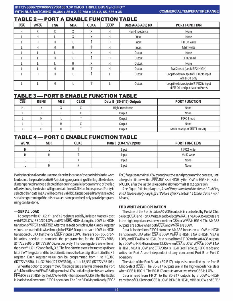
FIFO WRITE/READ OPERATIONThe state of the Port A data (A0-A35) outputs is controlled by Port A Chip
Select (CSA) and Port A Write/Read Select (W/RA). The A0-A35 outputs arein the high-impedance state when either CSA or W/RA is HIGH. The A0-A35outputs are active when both CSA and W/RA are LOW.
Data is loaded into FIFO1 from the A0-A35 inputs on a LOW-to-HIGHtransition of CLKA when CSA is LOW, W/RA is HIGH, ENA is HIGH, MBA isLOW, and FFA/IRA is HIGH. Data is read from FIFO2 to the A0-A35 outputsby a LOW-to-HIGH transition of CLKA when CSA is LOW, W/RA is LOW, ENAis HIGH, MBA is LOW, and EFA/ORA is HIGH (see Table 2). FIFO reads andwrites on Port A are independent of any concurrent Port B or Port Coperation.
The state of the Port B data (B0-B17) outputs is controlled by the Port BChip Select (CSB). The B0-B17 outputs are in the high-impedance statewhen CSB is HIGH. The B0-B17 outputs are active when CSB is LOW.
Data is read from FIFO1 to the B0-B17 outputs by a LOW-to-HIGHtransition of CLKB when CSB is LOW, RENB is HIGH, MBB is LOW and EFB/
TABLE 2 ⎯⎯⎯⎯⎯ PORT A ENABLE FUNCTION TABLE

14
COMMERCIAL TEMPERATURE RANGEIDT72V3686/72V3696/72V36106 3.3V CMOS TRIPLE BUS SyncFIFOTM
WITH BUS-MATCHING 16,384 x 36 x 2, 32,768 x 36 x 2, 65, 536 x 36
TABLE 5 ⎯⎯⎯⎯⎯ FIFO1 FLAG OPERATION (IDT Standard and FWFT modes)
TABLE 6 ⎯⎯⎯⎯⎯ FIFO2 FLAG OPERATION (IDT Standard and FWFT modes)
Synchronized SynchronizedNumber of Words in FIFO Memory(1,2) to CLKB to CLKA
IDT72V3686(3) IDT72V3696(3) IDT72V36106(3) EFB/ORB AEB AFA FFA/IRA
0 0 0 L L H H
1 to X1 1 to X1 1 to X1 H L H H
(X1+1) to [16,384-(Y1+1)] (X1+1) to [32,768-(Y1+1)] (X1+1) to [65,536-(Y1+1)] H H H H
(16,384-Y1) to 16,383 (32,768-Y1) to 32,767 (65,536-Y1) to 65,535 H H L H
16,384 32,768 65,536 H H L L
NOTES:1. When a word loaded to an empty FIFO is shifted to the output register, its previous FIFO memory location is free.2. Data in the output register does not count as a "word in FIFO memory". Since in FWFT mode, the first word written to an empty FIFO goes unrequested to the output register (no read operation
necessary), it is not included in the FIFO memory count.3. X1 is the almost-empty offset for FIFO1 used by AEB. Y1 is the almost-full offset for FIFO1 used by AFA. Both X1 and Y1 are selected during a FIFO1 reset or port A programming.4. The ORB and IRA functions are active during FWFT mode; the EFB and FFA functions are active in IDT Standard mode.
NOTES:1. When a word loaded to an empty FIFO is shifted to the output register, its previous FIFO memory location is free.2. Data in the output register does not count as a "word in FIFO memory". Since in FWFT mode, the first word written to an empty FIFO goes unrequested to the output register (no read operation
necessary), it is not included in the FIFO memory count.3. X2 is the almost-empty offset for FIFO2 used by AEA. Y2 is the almost-full offset for FIFO2 used by AFC. Both X2 and Y2 are selected during a FIFO2 reset or port A programming.4. The ORA and IRC functions are active during FWFT mode; the EFA and FFC functions are active in IDT Standard mode.
Synchronized SynchronizedNumber of Words in FIFO Memory(1,2) to CLKA to CLKC
IDT72V3686(3) IDT72V3696(3) IDT72V36106(3) EFA/ORA AEA AFC FFC/IRC
0 0 0 L L H H
1 to X2 1 to X2 1 to X2 H L H H
(X2+1) to [16,384-(Y2+1)] (X2+1) to [32,768-(Y2+1)] (X2+1) to [65,536-(Y2+1)] H H H H
(16,384-Y2) to 16,383 (32,768-Y2) to 32,767 (65,536-Y2) to 65,535 H H L H
16,384 32,768 65,536 H H L L
ORB is HIGH (see Table 3). FIFO reads on Port B are independent of anyconcurrent Port A and Port C operations.
Data is loaded into FIFO2 from the C0-C17 inputs on a LOW-to-HIGHtransition of CLKC when WENB is HIGH, MBC is LOW, and FFC/IRC is HIGH(see Table 4). FIFO writes on Port C are independent of any concurrent PortA and Port B operation.
The setup and hold time constraints for CSA and W/RA with regard to CLKAas well as CSB with regard to CLKB are only for enabling write and readoperations and are not related to high-impedance control of the data outputs.If ENA is LOW during a clock cycle, either CSA or W/RA may change statesduring the setup and hold time window of the cycle. This is also true for CSBwhen RENB is LOW.
When operating the FIFO in FWFT mode and the Output Ready flag is LOW,the next word written is automatically sent to the FIFO’s output register by theLOW-to-HIGH transition of the port clock that sets the Output Ready flag HIGH.When the Output Ready flag is HIGH, subsequent data is clocked to the outputregisters only when a read is selected using CSA, W/RA, ENA and MBA at PortA or using CSB, RENB and MBB at Port B.
When operating the FIFO in IDT Standard mode, the first word will cause theEmpty Flag to change state on the second LOW-to-HIGH transition of the ReadClock. The data word will not be automatically sent to the output register. Instead,data residing in the FIFO’s memory array is clocked to the output register onlywhen a read is selected using CSA, W/RA, ENA and MBA at Port A or usingCSB, RENB and MBB at Port B. Relevant write and read timing diagrams forPort A can be found in Figure 10 and 15. Relevant read and write timing
diagrams for Port B and Port C, together with Bus-Matching and Endian selectoperation, can be found in Figure 11 to 14.
LOOPBACK (LOOP)A Loopback function is provided on Port A and is selected by setting the LOOP
pin LOW. When the Loop feature is selected, the data output from FIFO2 will bedirected to the data input of FIFO1. If Loop is selected and Port A is set-up forwrite operation via the W/RA pin being HIGH, then data output from FIFO2 willbe written to FIFO1, on every LOW-to-HIGH transition of CLKA, provided CSAis LOW and ENA is HIGH. However, FIFO2 data output will not be placed onthe output Port A (A0-A35). If Port A is set-up for read operation via the W/RApin being LOW, then data output from FIFO2 will be written into FIFO1 on everyLOW-to-HIGH transition of CLKA, provided CSA is LOW and ENA is HIGH. AlsoFIFO2 data will be output to Port A (A0-A35). When the LOOP pin is HIGH thenPort A operates in the normal manner. Refer to Table 2 for the input set-up ofthe Loop feature.
The Loop operation will continue to happen provided that FIFO1 is not fulland FIFO2 is not empty. If during a Loop sequence FIFO1 becomes full thenany data that continues to be read out from FIFO2 will only be placed on thePort A (A0-A35) lines, (provided that Port A is set-up for read operation). Ifduring a Loop sequence the FIFO2 becomes empty, then the last word fromFIFO2 will continue to be clocked into FIFO1 until FIFO1 becomes full or untilthe Loop function is stopped. The Loop feature can be useful when performingsystem debugging and remote loopbacks. See Figures 34 and 35 for Loopbacktiming diagrams.

15
COMMERCIAL TEMPERATURE RANGEIDT72V3686/72V3696/72V36106 3.3V CMOS TRIPLE BUS SyncFIFOTM
WITH BUS-MATCHING 16,384 x 36 x 2, 32,768 x 36 x 2, 65, 536 x 36
SYNCHRONIZED FIFO FLAGSEach FIFO is synchronized to its port clock through at least two flip-flop stages.
This is done to improve flag signal reliability by reducing the probability ofmetastable events when CLKA operates asynchronously with respect to eitherCLKB or CLKC. EFA/ORA, AEA, FFA/IRA, and AFA are synchronized toCLKA. EFB/ORB and AEB are synchronized to CLKB. FFC/IRC and AFC aresynchronized to CLKC. Tables 5 and 6 show the relationship of each port flagto FIFO1 and FIFO2.
EMPTY/OUTPUT READY FLAGS (EFA/ORA, EFB/ORB)These are dual purpose flags. In the FWFT mode, the Output Ready (ORA,
ORB) function is selected. When the Output Ready flag is HIGH, new data ispresent in the FIFO output register. When the Output Ready flag is LOW, theprevious data word is present in the FIFO output register and attempted FIFOreads are ignored.
In the IDT Standard mode, the Empty Flag (EFA, EFB) function is selected.When the Empty Flag is HIGH, data is available in the FIFO’s RAM memory forreading to the output register. When the Empty Flag is LOW, the previous dataword is present in the FIFO output register and attempted FIFO reads areignored.
The Empty/Output Ready flag of a FIFO is synchronized to the port clock thatreads data from its array. For both the FWFT and IDT Standard modes, the FIFOread pointer is incremented each time a new word is clocked to its output register.The state machine that controls an Output Ready flag monitors a write pointerand read pointer comparator that indicates when the FIFO memory status isempty, empty+1, or empty+2.
In FWFT mode, from the time a word is written to a FIFO, it can be shifted tothe FIFO output register in a minimum of three cycles of the Output Ready flagsynchronizing clock. Therefore, an Output Ready flag is LOW if a word inmemory is the next data to be sent to the FlFO output register and three cyclesof the port clock that reads data from the FIFO have not elapsed since the timethe word was written. The Output Ready flag of the FIFO remains LOW until thethird LOW-to-HIGH transition of the synchronizing clock occurs, simultaneouslyforcing the Output Ready flag HIGH and shifting the word to the FIFO outputregister.
In IDT Standard mode, from the time a word is written to a FIFO, the EmptyFlag will indicate the presence of data available for reading in a minimum of twocycles of the Empty Flag synchronizing clock. Therefore, an Empty Flag is LOWif a word in memory is the next data to be sent to the FlFO output register andtwo cycles of the port Clock that reads data from the FIFO have not elapsed sincethe time the word was written. The Empty Flag of the FIFO remains LOW untilthe second LOW-to-HIGH transition of the synchronizing clock occurs, forcingthe Empty Flag HIGH; only then can data be read.
A LOW-to-HIGH transition on an Empty/Output Ready flag synchronizingclock begins the first synchronization cycle of a write if the clock transition occursat time tSKEW1 or greater after the write. Otherwise, the subsequent clock cyclecan be the first synchronization cycle (see Figure 16, 17, 18 and 19).
FULL/INPUT READY FLAGS (FFA/IRA, FFC/IRC)These are dual purpose flags. In FWFT mode, the Input Ready (IRA and
IRC) function is selected. In IDT Standard mode, the Full Flag (FFA and FFC)function is selected. For both timing modes, when the Full/Input Ready flag isHIGH, a memory location is free in the FIFO to receive new data. No memorylocations are free when the Full/Input Ready flag is LOW and attempted writesto the FIFO are ignored.
The Full/Input Ready flag of a FlFO is synchronized to the port clock that writesdata to its array. For both FWFT and IDT Standard modes, each time a wordis written to a FIFO, its write pointer is incremented. The state machine that
controls a Full/Input Ready flag monitors a write pointer and read pointercomparator that indicates when the FlFO memory status is full, full-1, or full-2.From the time a word is read from a FIFO, its previous memory location is readyto be written to in a minimum of two cycles of the Full/Input Ready flagsynchronizing clock. Therefore, an Full/Input Ready flag is LOW if less than twocycles of the Full/Input Ready flag synchronizing clock have elapsed since thenext memory write location has been read. The second LOW-to-HIGH transitionon the Full/Input Ready flag synchronizing clock after the read sets the Full/InputReady flag HIGH.
A LOW-to-HIGH transition on a Full/Input Ready flag synchronizing clockbegins the first synchronization cycle of a read if the clock transition occurs attime tSKEW1 or greater after the read. Otherwise, the subsequent clock cyclecan be the first synchronization cycle (see Figure 20, 21, 22, and 23).
ALMOST-EMPTY FLAGS (AEA, AEB)The Almost-Empty flag of a FIFO is synchronized to the port clock that reads
data from its array. The state machine that controls an Almost-Empty flag monitorsa write pointer and read pointer comparator that indicates when the FIFOmemory status is almost-empty, almost-empty+1, or almost-empty+2. Thealmost-empty state is defined by the contents of register X1 for AEB and registerX2 for AEA. These registers are loaded with preset values during a FIFO reset,programmed from Port A, or programmed serially (see the Almost-Empty flagand Almost-Full flag offset programming section). An Almost-Empty flag is LOWwhen its FIFO contains X or less words and is HIGH when its FIFO contains(X+1) or more words. A data word present in the FIFO output register has beenread from memory.
Two LOW-to-HIGH transitions of the Almost-Empty flag synchronizing clockare required after a FIFO write for its Almost-Empty flag to reflect the new levelof fill. Therefore, the Almost-Full flag of a FIFO containing (X+1) or more wordsremains LOW if two cycles of its synchronizing clock have not elapsed since thewrite that filled the memory to the (X+1) level. An Almost-Empty flag is set HIGHby the second LOW-to-HIGH transition of its synchronizing clock after the FIFOwrite that fills memory to the (X+1) level. A LOW-to-HIGH transition of an Almost-Empty flag synchronizing clock begins the first synchronization cycle if it occursat time tSKEW2 or greater after the write that fills the FIFO to (X+1) words.Otherwise, the subsequent synchronizing clock cycle may be the first synchro-nization cycle. (See Figure 24 and 25).
ALMOST-FULL FLAGS (AFA, AFC)The Almost-Full flag of a FIFO is synchronized to the port clock that writes
data to its array. The state machine that controls an Almost-Full flag monitors awrite pointer and read pointer comparator that indicates when the FIFO memorystatus is almost-full, almost-full-1, or almost-full-2. The almost-full state is definedby the contents of register Y1 for AFA and register Y2 for AFC. These registersare loaded with preset values during a FlFO reset, programmed from Port A,or programmed serially (see Almost-Empty flag and Almost-Full flag offsetprogramming section). An Almost-Full flag is LOW when the number of wordsin its FIFO is greater than or equal to (16,384-Y), (32,768-Y), or (65,536-Y)for the IDT72V3686, IDT72V3696, or IDT72V36106 respectively. An Almost-Full flag is HIGH when the number of words in its FIFO is less than or equal to[16,384-(Y+1)], [32,768-(Y+1)], or [65,536-(Y+1)] for the IDT72V3686,IDT72V3696, or IDT72V36106 respectively. Note that a data word present inthe FIFO output register has been read from memory.
Two LOW-to-HIGH transitions of the Almost-Full flag synchronizing clock arerequired after a FIFO read for its Almost-Full flag to reflect the new level of fill.Therefore, the Almost-Full flag of a FIFO containing [16,384/32,768/65,536-(Y+1)] or less words remains LOW if two cycles of its synchronizing clock havenot elapsed since the read that reduced the number of words in memory to

16
COMMERCIAL TEMPERATURE RANGEIDT72V3686/72V3696/72V36106 3.3V CMOS TRIPLE BUS SyncFIFOTM
WITH BUS-MATCHING 16,384 x 36 x 2, 32,768 x 36 x 2, 65, 536 x 36
[16,384/32,768/65,536-(Y+1)]. An Almost-Full flag is set HIGH by the secondLOW-to-HIGH transition of its synchronizing clock after the FIFO read thatreduces the number of words in memory to [16,384/32,768/65,536-(Y+1)]. ALOW-to-HIGH transition of an Almost-Full flag synchronizing clock begins thefirst synchronization cycle if it occurs at time tSKEW2 or greater after the read thatreduces the number of words in memory to [16,384/32,768/65,536-(Y+1)].Otherwise, the subsequent synchronizing clock cycle may be the first synchro-nization cycle (see Figure 26 and 27).
MAILBOX REGISTERSEach FIFO has an 18-bit bypass register allowing the passage of command
and control information from Port A to Port B or from Port C to Port A without puttingit in queue. The Mailbox Select (MBA, MBB and MBC) inputs choose betweena mail register and a FIFO for a port data transfer operation. The usable widthof both the Mail1 and Mail2 registers matches the selected bus size for ports Band C.
When sending data from Port A to Port B via the Mail1 Register, the followingis the case: A LOW-to-HIGH transition on CLKA writes data to the Mail1 Registerwhen a Port A write is selected by CSA, W/RA, and ENA with MBA HIGH. Ifthe selected Port B bus size is 18 bits, then the usable width of the Mail1 Registeremploys data lines A0-A17. (In this case, A18-A35 are don’t care inputs.) Ifthe selected Port B bus size is 9 bits, then the usable width of the Mail1 Registeremploys data lines A0-A8. (In this case, A9-A35 are don’t care inputs.)
When sending data from Port C to Port A via the Mail2 Register, the followingis the case: A LOW-to-HIGH transition on CLKC writes data to the Mail2 Registerwhen a Port C write is selected by WENC with MBC HIGH. If the selected PortC bus size is 18 bits, then the usable width of the Mail2 Register employs datalines C0-C17. If the selected Port C bus size is 9 bits, then the usable width ofthe Mail2 Register employs data lines C0-C8. (In this case, C9-C17 are don’tcare inputs.)
Writing data to a mail register sets its corresponding flag (MBF1 or MBF2)LOW. Attempted writes to a mail register are ignored while the mail flag is LOW.
When data outputs of a port are active, the data on the bus comes from theFIFO output register when the port Mailbox select input is LOW and from themail register when the port mailbox select input is HIGH.
The Mail1 Register Flag (MBF1) is set HIGH by a LOW-to-HIGH transitionon CLKB when a Port B read is selected by CSB, and RENB with MBB HIGH.For an 18-bit bus size, 18 bits of mailbox data are placed on B0-B17. For the9-bit bus size, 9 bits of mailbox data are placed on B0-B8. (In this case, B9-B17are indeterminate.)
The Mail2 Register Flag (MBF2) is set HIGH by a LOW-to-HIGH transitionon CLKA when a Port A read is selected by CSA, W/RA, and ENA with MBAHIGH. The data in a mail register remains intact after it is read and changes onlywhen new data is written to the register. For an 18-bit bus size, 18 bits of mailboxdata appear on A18-A35. (In this case, A0-A17 are indeterminate.) For a 9-bit bus size, 9 bits of mailbox data appear on A18-A26. (In this case, A0-A17and A27-A35 are indeterminate.)
The data in a mail register remains intact after it is read and changes onlywhen new data is written to the register. The Endian Select feature has no effecton mailbox data.
Note that MBC must be HIGH during Master Reset (until FFA/IRA and FFC/IRC go HIGH. MBA and MBB are don't care inputs during Master Reset. Formail register and mail register flag timing diagrams, see Figure 28 and 29.
BUS SIZINGPort B may be configured in either an 18-bit word or a 9-bit byte format for
data read from FIFO1. Port C may be configured in either an 18-bit word ora 9-bit byte format for data written to FIFO2. The bus size can be selectedindependently for Ports B and C. The level applied to the Port B Size Select(SIZEB) input determines the Port B bus size and the level applied to the PortC Size Select (SIZEC) input determines the Port C bus size. These levels shouldbe static throughout FIFO operation. Both bus size selections are implementedat the completion of Master Reset, by the time the Full/Input Ready flag is setHIGH, as shown in Figure 2 and 3.
Two different methods for sequencing data transfer are available for PortsB and C regardless of whether the bus size selection is byte- or word-size. Theyare referred to as Big-Endian (most significant byte first) and Little-Endian (leastsignificant byte first). The level applied to the Big-Endian Select (BE) input duringthe LOW-to-HIGH transition of MRS1 and MRS2 selects the endian method thatwill be active during FIFO operation. This selection applies to both ports B andC. The endian method is implemented at the completion of Master Reset, bythe time the Full/Input Ready flag is set HIGH, as shown in Figure 2 and 3 (seeEndian Selection section).
Only 36-bit long word data is written to or read from the two FIFO memorieson these devices. Bus-Matching operations are done after data is read fromthe FIFO1 RAM (Port B) and before data is written to the FIFO2 RAM (PortC). The Endian select operations are not available when transferring data viamailbox registers. Furthermore, both the word- and byte-size bus selectionslimit the width of the data bus that can be used for mail register operations. Inthis case, only those byte lanes belonging to the selected word- or byte-sizebus can carry mailbox data. The remaining data outputs will be indeterminate.The remaining data inputs will be don’t care inputs. For example, when a word-size bus is selected on Port B, then mailbox data can be transmitted only fromA0-A17 to B0-B17. When a byte-size bus is selected on Port B, then mailboxdata can be transmitted only from A0-A8 to B0-B8. Similarly, when a word-sizebus is selected on Port C, then mailbox data can be transmitted only from C0-C17 to A18-A35. When a byte-size bus is selected on Port C, then mailbox datacan be transmitted only from C0-C8 to A18-A26.
BUS-MATCHING FIFO1 READSData is read from the FIFO1 RAM in 36-bit long word increments. Since Port
B can have a byte or word size, only the first one or two bytes appear on theselected portion of the FIFO1 output register, with the rest of the long word storedin auxiliary registers. In this case, subsequent FIFO1 reads output the rest ofthe long word to the FIFO1 output register in the order shown by Figure 2.
When reading data from FIFO1 in byte format, the unused B9-B17 outputsare indeterminate.
BUS-MATCHING FIFO2 WRITESData is written to the FIFO2 RAM in 36-bit long word increments. Data written
to FIFO2 with a byte or word bus size stores the initial bytes or words in auxiliaryregisters. The CLKC rising edge that writes the fourth byte or the second wordof long word to FIFO2 also stores the entire long word in the FIFO2 memory.The bytes are arranged in the manner shown in Figure 3.
When writing data to FIFO2 in byte format, the unused C9-C17 inputs aredon't care inputs.

17
COMMERCIAL TEMPERATURE RANGEIDT72V3686/72V3696/72V36106 3.3V CMOS TRIPLE BUS SyncFIFOTM
WITH BUS-MATCHING 16,384 x 36 x 2, 32,768 x 36 x 2, 65, 536 x 36
Figure 2. Port B Bus Sizing
A
A
D
A
C
B
B
C
B
D
C
C
A
D
D
B
Write to FIFO1
1st: Read from FIFO1
L L
BYTE ORDER ON PORT A:
BE SIZEB
2nd: Read from FIFO1
3rd: Read from FIFO1
4th: Read from FIFO1
1st: Read from FIFO1
1st: Read from FIFO1
2nd: Read from FIFO1
2nd: Read from FIFO1
H H
BE SIZEB
H L
BE SIZEB
D
C
1st: Read from FIFO1
A
B
BE SIZEBL H
2nd: Read from FIFO1
3rd: Read from FIFO1
4th: Read from FIFO1
4676 drw04
BYTE ORDER ON PORT B:
A35⎯A27 A26⎯A18 A17⎯A9 A8 ⎯A0
B17⎯B9 B8 ⎯B0
B17⎯B9 B8 ⎯B0
B17⎯B9 B8 ⎯B0
B17⎯B9 B8 ⎯B0
B17⎯B9 B8 ⎯B0
B17⎯B9 B8 ⎯B0
B17⎯B9 B8 ⎯B0
B17⎯B9 B8 ⎯B0
B17⎯B9 B8 ⎯B0
B17⎯B9 B8 ⎯B0
B17⎯B9 B8 ⎯B0
B17⎯B9 B8 ⎯B0
(b) WORD SIZE ⎯ BIG ENDIAN
(c) WORD SIZE ⎯ LITTLE ENDIAN
(d) BYTE SIZE ⎯ BIG ENDIAN
(e) BYTE SIZE ⎯ LITTLE ENDIAN

18
COMMERCIAL TEMPERATURE RANGEIDT72V3686/72V3696/72V36106 3.3V CMOS TRIPLE BUS SyncFIFOTM
WITH BUS-MATCHING 16,384 x 36 x 2, 32,768 x 36 x 2, 65, 536 x 36
Figure 3. Port C Bus Sizing
A
A
D
A
C
B
B
C
B
D
C
C
A
D
D
B
Read from FIFO2
1st: Write to FIFO2
L L
BYTE ORDER ON PORT A:
BE SIZEC
2nd: Write to FIFO2
3rd: Write to FIFO2
4th: Write to FIFO2
1st: Write to FIFO2
1st: Write to FIFO2
2nd: Write to FIFO2
2nd: Write to FIFO2
H H
BE SIZEC
H L
BE SIZEC
D
C
1st: Write to FIFO2
A
B
BE SIZECL H
2nd: Write to FIFO2
3rd: Write to FIFO2
4th: Write to FIFO2
4676 drw05
BYTE ORDER ON PORT C:
A35⎯A27 A26⎯A18 A17⎯A9 A8 ⎯A0
C17⎯C9 C8 ⎯C0
(b) WORD SIZE ⎯ BIG ENDIAN
(c) WORD SIZE ⎯ LITTLE ENDIAN
(d) BYTE SIZE ⎯ BIG ENDIAN
(e) BYTE SIZE ⎯ LITTLE ENDIAN
C17⎯C9 C8 ⎯C0
C17⎯C9 C8 ⎯C0
C17⎯C9 C8 ⎯C0
C17⎯C9 C8 ⎯C0
C17⎯C9 C8 ⎯C0
C17⎯C9 C8 ⎯C0
C17⎯C9 C8 ⎯C0
C17⎯C9 C8 ⎯C0
C8 ⎯C0C17⎯C9
C8 ⎯C0C17⎯C9
C8 ⎯C0C17⎯C9

19
COMMERCIAL TEMPERATURE RANGEIDT72V3686/72V3696/72V36106 3.3V CMOS TRIPLE BUS SyncFIFOTM
WITH BUS-MATCHING 16,384 x 36 x 2, 32,768 x 36 x 2, 65, 536 x 36
NOTES:1. PRS2 and MBC must be HIGH during Master Reset until the rising edge of FFC/IRC goes HIGH.2. If BE/FWFT is HIGH, then EFA/ORA will go LOW one CLKA cycle earlier than in this case where BE/FWFT is LOW.3. MRS2 must toggle simultaneously with MRS1.
Figure 5. FIFO2 Master Reset and Loading X2 and Y2 with a Preset Value of Eight (IDT Standard and FWFT Modes)
Figure 4. FIFO1 Master Reset and Loading X1 and Y1 with a Preset Value of Eight (IDT Standard and FWFT Modes)
NOTES:1. PRS1 and MBC must be HIGH during Master Reset until the rising edge of FFA/IRA goes HIGH.2. If BE/FWFT is HIGH, then EFB/ORB will go LOW one CLKB cycle earlier than in this case where BE/FWFT is LOW.
CLKA
MRS1
FFA/IRA
AEB
AFA
MBF1
CLKB
EFB/ORB
FS2,FS1,FS0
4676 drw06
tRSTS tRSTH
tFSHtFSS
tWFF tWFF
tREF
tRSF
0,1
tRSF
tRSF
BEBE/FWFT FWFT
tBES tBEH
1 2
tFWS
(2)
LOOP
RTM LOW
HIGH
CLKC
MRS2(3)
FFC/IRC
AEA
AFC
MBF2
CLKA
EFA/ORA
FS2,FS1,FS0
4676 drw07
tRSTS tRSTH
tFSHtFSS
tWFF tWFF
tREF
tRSF
0,1
tRSF
tRSF
BEBE/FWFT FWFT
tBES tBEH
1 2
tFWS
(2)
LOOP
RTM LOW
HIGH

20
COMMERCIAL TEMPERATURE RANGEIDT72V3686/72V3696/72V36106 3.3V CMOS TRIPLE BUS SyncFIFOTM
WITH BUS-MATCHING 16,384 x 36 x 2, 32,768 x 36 x 2, 65, 536 x 36
NOTES:1. MRS1 must be HIGH during Partial Reset.2. If BE/FWFT is HIGH, then EFB/ORB will go LOW one CLKB cycle earlier than in this case where BE/FWFT is LOW.
Figure 6. FIFO1 Partial Reset (IDT Standard and FWFT Modes)
Figure 7. FIFO2 Partial Reset (IDT Standard and FWFT Modes)
NOTES:1. MRS2 must be HIGH during Partial Reset.2. If BE/FWFT is HIGH, then EFA/ORA will go LOW one CLKA cycle earlier than in this case where BE/FWFT is LOW.
CLKA
PRS1
FFA/IRA
AEB
AFA
MBF1
CLKB
EFB/ORB
4676 drw08
tRSTS tRSTH
tWFFtWFF
tREF
tRSF
tRSF
tRSF
1 2
(2)
RTM LOW
CLKC
PRS2
FFC/IRC
AEA
AFC
MBF1
CLKA
EFA/ORA
4676 drw09
tRSTS tRSTH
tWFFtWFF
tREF
tRSF
tRSF
tRSF
(2)

21
COMMERCIAL TEMPERATURE RANGEIDT72V3686/72V3696/72V36106 3.3V CMOS TRIPLE BUS SyncFIFOTM
WITH BUS-MATCHING 16,384 x 36 x 2, 32,768 x 36 x 2, 65, 536 x 36
Figure 9. Serial Programming of the Almost-Full Flag and Almost-Empty Flag Offset Values after Reset (IDT Standard and FWFT Modes)
NOTES:1. tSKEW1 is the minimum time between the rising CLKA edge and a rising CLKC edge for FFC/IRC to transition HIGH in the next cycle. If the time between the rising edge of CLKA and rising
edge of CLKC is less than tSKEW1, then FFC/IRC may transition HIGH one CLKC cycle later than shown.2. It is not necessary to program Offset register bits on consecutive clock cycles. FIFO write attempts are ignored until FFA/IRA, FFC/IRC is set HIGH.3. Programmable offsets are written serially to the SD input in the order AFA offset (Y1), AEB offset (X1), AFC offset (Y2), and AEA offset (X2).
NOTES:1. tSKEW1 is the minimum time between the rising CLKA edge and a rising CLKC edge for FFC/IRC to transition HIGH in the next cycle. If the time between the rising edge of CLKA and rising
edge of CLKC is less than tSKEW1, then FFC/IRC may transition HIGH one CLKC cycle later than shown.2. CSA = LOW, W/RA = HIGH, MBA = LOW. It is not necessary to program Offset register on consecutive clock cycles.
Figure 8. Parallel Programming of the Almost-Full Flag and Almost-Empty Flag Offset Values after Reset (IDT Standard and FWFT Modes)
4676 drw10
CLKA
MRS1,MRS2
FFA/IRA
CLKC
FFC/IRC
A0-A35
FS1,FS0
ENA
tFSH
tWFF
tENHtENS2 tSKEW1
tDStDH
tWFF
4
0,0
AFA Offset(Y1)
AEB Offset(X1)
AFC Offset(Y2)
AEA Offset(X2)
First Word to FIFO1
1 2
(1)
tFSHtFSS
tFSS
FS2
CLKA
FFA/IRA
tSENS tSENH
FS0/SD(3)
tSPH tSENS tSENHtFSS
tWFF
FS1/SEN
AEA Offset(X2) LSB
tSDS tSDH tSDS tSDH
AFA Offset(Y1) MSB
MRS1,MRS2
4
4676 drw11
tFSS tFSH
CLKC 4
FS2
FFC/IRC
tWFF
tSKEW(1)

22
COMMERCIAL TEMPERATURE RANGEIDT72V3686/72V3696/72V36106 3.3V CMOS TRIPLE BUS SyncFIFOTM
WITH BUS-MATCHING 16,384 x 36 x 2, 32,768 x 36 x 2, 65, 536 x 36
NOTE:1. Written to FIFO1.
Figure 10. Port A Write Cycle Timing for FIFO1 (IDT Standard and FWFT Modes)
Figure 11. Port C Word Write Cycle Timing for FIFO2 (IDT Standard and FWFT Modes)
DATA SIZE TABLE FOR WORD WRITES TO FIFO2
NOTE:1. BE is selected at Master Reset; SIZEB and SIZEC must be static throughout device operation.
SIZE MODE(1) WRITE DATA WRITTEN DATA READ FROM FIFO2
NO. TO FIFO2
SIZEC BE C17-C9 C8-C0 A35-A27 A26-A18 A17-A9 A8-A0
L H 1 A B A B C D2 C D
L L 1 C D A B C D2 A B
4676 drw12
CLKA
FFA/IRA
ENA
A0-A35
MBA
CSA
W/RA
tCLK
tCLKH tCLKL
tENH
tENH
tENH
tENH
tDH
W1(1) W2(1)
tENS2
tDS
tENS2
tENS2
tENS1
tENS1
tENHtENH tENS2
No Operation
HIGH
CLKC
WENC
tENH tENH
FFC/IRC HIGH
4676 drw13
C0-C17
tENHtENH
MBC
tDHtDS
tENS2
tENS2 tENS2
tENS2

23
COMMERCIAL TEMPERATURE RANGEIDT72V3686/72V3696/72V36106 3.3V CMOS TRIPLE BUS SyncFIFOTM
WITH BUS-MATCHING 16,384 x 36 x 2, 32,768 x 36 x 2, 65, 536 x 36
DATA SIZE TABLE FOR WORD READS FROM FIFO1SIZE MODE(1) DATA WRITTEN TO FIFO1 READ DATA READ FROM FIFO1
NO.
Figure 13. Port B Word Read Cycle Timing for FIFO1 (IDT Standard and FWFT Modes)
Figure 12. Port C Byte Write Cycle Timing for FIFO2 (IDT Standard and FWFT Modes)
NOTE:1. BE is selected at Master Reset; SIZEB and SIZEC must be static throughout device operation.
SIZE MODE(1) WRITE DATA WRITTEN DATA READ FROM FIFO2NO. TO FIFO2
SIZEC BE C8-C0 A35-A27 A26-A18 A17-A9 A8-A0
H H A B C D
H L A B C D
1 A2 B3 C4 D1 D2 C3 B4 A
DATA SIZE TABLE FOR BYTE WRITES TO FIFO2
NOTE:1. BE is selected at Master Reset; SIZEB and SIZEC must be static throughout device operation.
FFC/IRC
CLKC
tENHtENS2
WENC
4676 drw14
HIGH
C0-C8
tENS2 tENH
tENS2
tENH
tDS tDH
tENH
MBC
CLKB
RENB
EFB/ORB
CSB
HIGH
4676 drw15
B0-B17 Previous Data
tDIStAtA
tENS2 tENH
No Operation
Read 1B0-B17tA tA
Read 1
Read 2
Read 2
Read 3
tDIS
MBB
(Standard Mode)
(FWFT Mode)
OR
tENtMDV
tMDVtEN
SIZEB BE A35-A27 A26-A18 A17-A9 A8-A0 B17-B9 B8-B0H H A B C D 1 A B
2 C D
H L A B C D 1 C D
2 A B
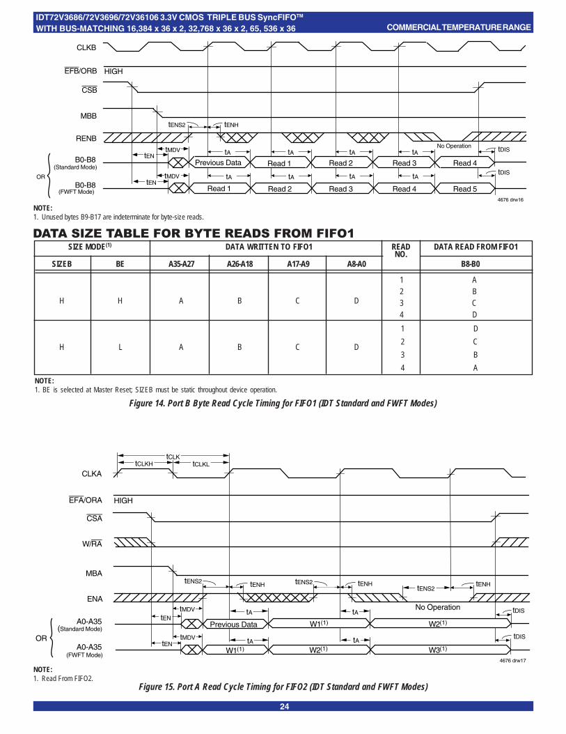
24
COMMERCIAL TEMPERATURE RANGEIDT72V3686/72V3696/72V36106 3.3V CMOS TRIPLE BUS SyncFIFOTM
WITH BUS-MATCHING 16,384 x 36 x 2, 32,768 x 36 x 2, 65, 536 x 36
DATA SIZE TABLE FOR BYTE READS FROM FIFO1SIZE MODE(1) DATA WRITTEN TO FIFO1 READ DATA READ FROM FIFO1
NO.SIZEB BE A35-A27 A26-A18 A17-A9 A8-A0 B8-B0
H H A B C D
H L A B C D
1 A2 B3 C4 D
1 D
2 C
3 B
4 A
NOTE:1. Unused bytes B9-B17 are indeterminate for byte-size reads.
NOTE:1. BE is selected at Master Reset; SIZEB must be static throughout device operation.
Figure 14. Port B Byte Read Cycle Timing for FIFO1 (IDT Standard and FWFT Modes)
NOTE:1. Read From FIFO2.
Figure 15. Port A Read Cycle Timing for FIFO2 (IDT Standard and FWFT Modes)
EFB/ORB
MBB
CSB
RENB
CLKB
4676 drw16
HIGH
B0-B8
B0-B8 Read 5Read 2 Read 3
Read 4Read 1 Read 3
Read 4
Previous Data Read 2
No Operation tDIS
tDIS
tA
tAtA
tAtA
tA
tENS2 tENH
tA
tA
Read 1
(Standard Mode)
(FWFT Mode)
tENtMDV
tMDVtEN
OR
4676 drw17
CLKA
EFA/ORA
ENA
MBA
CSA
W/RA
tCLKtCLKH tCLKL
tENS2
tAtMDVtEN
tA
tENS2 tENHtENS2
tENH
W1(1)
tENH
tDISNo Operation
A0-A35 tENtDIS
Previous Data
tMDV tAOR tAW2(1)
W1(1) W2(1)
W3(1)(FWFT Mode)
(Standard Mode)A0-A35
HIGH

25
COMMERCIAL TEMPERATURE RANGEIDT72V3686/72V3696/72V36106 3.3V CMOS TRIPLE BUS SyncFIFOTM
WITH BUS-MATCHING 16,384 x 36 x 2, 32,768 x 36 x 2, 65, 536 x 36
NOTES:1. tSKEW1 is the minimum time between a rising CLKA edge and a rising CLKB edge for ORB to transition HIGH and to clock the next word to the FIFO1 output register in three CLKB cycles.
If the time between the rising CLKA edge and rising CLKB edge is less than tSKEW1, then the transition of ORB HIGH and load of the first word to the output register may occur one CLKBcycle later than shown.
2. If Port B size is word or byte, ORB is set LOW by the last word or byte read from FIFO1, respectively (the word-size case is shown).
Figure 16. ORB Flag Timing and First Data Word Fall Through when FIFO1 is Empty (FWFT Mode)
CSA
WRA
MBA
A0-A35
CLKB
ORB
CSB
MBB
ENA
RENB
B0-B17
CLKA
1 2
4676 drw18
tCLKH tCLKLtCLK
tENS2
tENS2
tENH
tENH
tDS tDH
tSKEW1tCLK
tCLKL
tENS2
tARead 1
FIFO1 Empty
LOW
HIGH
LOW
LOW
tCLKH
W1
HIGH
(1)
tREF tREF
Read 2
tENH
tA
IRA
3

26
COMMERCIAL TEMPERATURE RANGEIDT72V3686/72V3696/72V36106 3.3V CMOS TRIPLE BUS SyncFIFOTM
WITH BUS-MATCHING 16,384 x 36 x 2, 32,768 x 36 x 2, 65, 536 x 36
NOTES:1. tSKEW1 is the minimum time between a rising CLKA edge and a rising CLKB edge for EFB to transition HIGH in the next CLKB cycle. If the time between the rising CLKA edge and rising
CLKB edge is less than tSKEW1, then the transition of EFB HIGH may occur one CLKB cycle later than shown.2. If Port B size is word or byte, EFB is set LOW by the last word or byte read from FIFO1, respectively (the word-size case is shown).
Figure 17. EFBEFBEFBEFBEFB Flag Timing and First Data Read Fall Through when FIFO1 is Empty (IDT Standard Mode)
CSA
WRA
MBA
FFA
A0-A35
CLKB
CSB
MBB
ENA
RENB
B0-B17
CLKA
1 2
4676 drw 19
tCLKH tCLKLtCLK
tENS2
tENS2
tENH
tENH
tDS tDH
tSKEW1tCLK
tCLKL
tENS2
tARead 1
FIFO1 Empty
LOW
HIGH
LOW
LOW
tCLKH
W1
HIGH
(1)
tREF tREF
Read 2
tENH
tA
EFB

27
COMMERCIAL TEMPERATURE RANGEIDT72V3686/72V3696/72V36106 3.3V CMOS TRIPLE BUS SyncFIFOTM
WITH BUS-MATCHING 16,384 x 36 x 2, 32,768 x 36 x 2, 65, 536 x 36
NOTES:1. tSKEW1 is the minimum time between a rising CLKC edge and a rising CLKA edge for ORA to transition HIGH and to clock the next word to the FIFO2 output register in three CLKA cycles.
If the time between the CLKC edge and the rising CLKA edge is less than tSKEW1, then the transition of ORA HIGH and load of the first word to the output register may occur one CLKAcycle later than shown.
2. If Port C size is word or byte, tSKEW1 is referenced to the rising CLKC edge that writes the last word or byte write of the long word, respectively.
Figure 18. ORA Flag Timing and First Data Word Fall through when FIFO2 is Empty (FWFT Mode)
MBC
C0-C17
CLKA
CSA
W/RA
MBA
WENC
ENA
A0-A35
CLKC
1 2
4676 drw 20
tCLKH tCLKLtCLK
tENS2
tENS2
tENH
tENH
tDS tDH
tSKEW1tCLK
tCLKL
tENS2 tENH
tAW1
FIFO2 Empty
LOW
LOW
LOW
tCLKH
HIGH
(1)
tREF
tDHtDS
Write 1 Write 2
ORA
IRC
3
Old Data in FIFO2 Output Register
tREF

28
COMMERCIAL TEMPERATURE RANGEIDT72V3686/72V3696/72V36106 3.3V CMOS TRIPLE BUS SyncFIFOTM
WITH BUS-MATCHING 16,384 x 36 x 2, 32,768 x 36 x 2, 65, 536 x 36
NOTES:1. tSKEW1 is the minimum time between a rising CLKC edge and a rising CLKA edge for EFA to transition HIGH in the next CLKA cycle. If the time between the rising CLKC edge and rising
CLKA edge is less than tSKEW1, then the transition of EFA HIGH may occur one CLKA cycle later than shown.2. If Port C size is word or byte, tSKEW1 is referenced to the rising CLKC edge that writes the last word or byte of the long word, respectively.
Figure 19. EFAEFAEFAEFAEFA Flag Timing and First Data Read when FIFO2 is Empty (IDT Standard Mode)
MBC
FFC
C0-C17
CLKA
EFA
CSA
W/RA
MBA
WENC
ENA
A0-A35
CLKC
1 2
4676 drw 21
tCLKH tCLKLtCLK
tENS2
tENS2
tENH
tENH
tDS tDH
tSKEW1 tCLKL
tENS2 tENH
tAW1
FIFO2 Empty
LOW
LOW
LOW
tCLKH
HIGH
(1)
tREFtREF
tDHtDS
Write 1 Write 2
tCLK
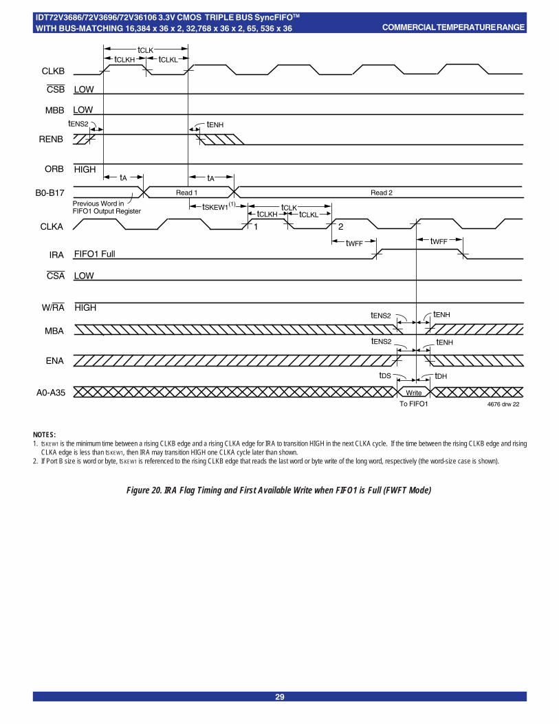
29
COMMERCIAL TEMPERATURE RANGEIDT72V3686/72V3696/72V36106 3.3V CMOS TRIPLE BUS SyncFIFOTM
WITH BUS-MATCHING 16,384 x 36 x 2, 32,768 x 36 x 2, 65, 536 x 36
NOTES:1. tSKEW1 is the minimum time between a rising CLKB edge and a rising CLKA edge for IRA to transition HIGH in the next CLKA cycle. If the time between the rising CLKB edge and rising
CLKA edge is less than tSKEW1, then IRA may transition HIGH one CLKA cycle later than shown.2. If Port B size is word or byte, tSKEW1 is referenced to the rising CLKB edge that reads the last word or byte write of the long word, respectively (the word-size case is shown).
Figure 20. IRA Flag Timing and First Available Write when FIFO1 is Full (FWFT Mode)
CSB
MBB
RENB
B0-B17
CLKB
CLKA
CSA
4676 drw 22
W/RA
1 2
A0-A35
MBA
ENA
tCLKtCLKH tCLKL
tENS2 tENH
tA
tSKEW1 tCLKtCLKH tCLKL
tENS2
tENS2
tDS
tENH
tENH
tDH
To FIFO1
Read 2
LOW
LOW
HIGH
LOW
HIGH
(1)
FIFO1 FulltWFF tWFF
Read 1
tA
Previous Word inFIFO1 Output Register
ORB
IRA
Write

30
COMMERCIAL TEMPERATURE RANGEIDT72V3686/72V3696/72V36106 3.3V CMOS TRIPLE BUS SyncFIFOTM
WITH BUS-MATCHING 16,384 x 36 x 2, 32,768 x 36 x 2, 65, 536 x 36
NOTES:1. tSKEW1 is the minimum time between a rising CLKB edge and a rising CLKA edge for FFA to transition HIGH in the next CLKA cycle. If the time between the rising CLKB edge and rising
CLKA edge is less than tSKEW1, then FFA may transition HIGH one CLKA cycle later than shown.2. If Port B size is word or byte, tSKEW1 is referenced from the rising CLKB edge that reads the last word or byte of the long word, respectively (the word-size case is shown).
Figure 21. FFAFFAFFAFFAFFA Flag Timing and First Available Write when FIFO1 is Full (IDT Standard Mode)
CSB
EFB
MBB
RENB
B0-B17
CLKB
FFA
CLKA
CSA
4676 drw 23
W/RA
1 2
A0-A35
MBA
ENA
tCLKtCLKH tCLKL
tENS2 tENH
tA
tSKEW1 tCLKtCLKH tCLKL
tENS2
tENS2
tDS
tENH
tENH
tDH
To FIFO1
Read 2
LOW
LOW
HIGH
LOW
HIGH
(1)
FIFO1 FulltWFF tWFF
Read 1
tA
Previous Word inFIFO1 Output Register
Write

31
COMMERCIAL TEMPERATURE RANGEIDT72V3686/72V3696/72V36106 3.3V CMOS TRIPLE BUS SyncFIFOTM
WITH BUS-MATCHING 16,384 x 36 x 2, 32,768 x 36 x 2, 65, 536 x 36
NOTES:1. tSKEW1 is the minimum time between a rising CLKC edge and a rising CLKC edge for IRC to transition HIGH in the next CLKC cycle. If the time between the rising CLKA edge and rising
CLKC edge is less than tSKEW1, then IRC may transition HIGH one CLKC cycle later than shown.2. If Port C size is word or byte, IRC is set LOW by the last word or byte write of the long word, respectively (the word-size case is shown).
Figure 22. IRC Flag Timing and First Available Write when FIFO2 is Full (FWFT Mode)
CSA
ORA
MBA
ENA
A0-A35
CLKA
IRC
CLKC
4676 drw 24
1 2
C0-C17
MBC
WENC
tCLKtCLKH tCLKL
tENS2 tENH
tA
tSKEW1 tCLKtCLKH tCLKL
tENS2
tENS2
tDS
tENH
tENH
tDH
To FIFO2
Previous Word in FIFO2 Output Register Next Word From FIFO2
LOW
W/RA LOW
LOW
HIGH
(1)
FIFO2 FulltWFF
tDH tDS
tWFF
Write

32
COMMERCIAL TEMPERATURE RANGEIDT72V3686/72V3696/72V36106 3.3V CMOS TRIPLE BUS SyncFIFOTM
WITH BUS-MATCHING 16,384 x 36 x 2, 32,768 x 36 x 2, 65, 536 x 36
NOTES:1. tSKEW2 is the minimum time between a rising CLKA edge and a rising CLKB edge for AEB to transition HIGH in the next CLKB cycle. If the time between the rising CLKA edge and rising
CLKB edge is less than tSKEW2, then AEB may transition HIGH one CLKB cycle later than shown.2. FIFO1 Write (CSA = LOW, W/RA = LOW, MBA = LOW), FIFO1 read (CSB = LOW, MBB = LOW). Data in the FIFO1 output register has been read from the FIFO.3. If Port B size is word or byte, AEB is set LOW by the last word or byte read from FIFO1, respectively.
Figure 24. Timing for AEBAEBAEBAEBAEB when FIFO1 is Almost-Empty (IDT Standard and FWFT Modes)
Figure 23. FFCFFCFFCFFCFFC Flag Timing and First Available Write when FIFO2 is Full (IDT Standard Mode)
NOTES:1. tSKEW1 is the minimum time between a rising CLKA edge and a rising CLKC edge for FFC to transition HIGH in the next CLKC cycle. If the time between the rising CLKA edge and rising
CLKC edge is less than tSKEW1, then FFC may transition HIGH one CLKC cycle later than shown.2. If Port C size is word or byte, FFC is set LOW by the last word or byte write of the long word, respectively (the word-size case is shown).
CSA
EFA
MBA
ENA
A0-A35
CLKA
FFC
CLKC
4676 drw 25
1 2
C0-C17
MBC
ENC
tCLKtCLKH tCLKL
tENS2 tENH
tA
tSKEW1 tCLKtCLKH tCLKL
tENS2
tENS2
tDS
tENH
tENH
tDH
To FIFO2
Previous Word in FIFO2 Output Register Next Word From FIFO2
LOW
W/RA LOW
LOW
HIGH
(1)
FIFO2 FulltWFF tWFF
tDH tDS
Write
AEB
CLKA
RENB4676 drw 26
ENA
CLKB 21
tENS2 tENH
tSKEW2
tPAE tPAE
tENS2 tENH
X1 Word in FIFO1 (X1+1) Words in FIFO1
(1)

33
COMMERCIAL TEMPERATURE RANGEIDT72V3686/72V3696/72V36106 3.3V CMOS TRIPLE BUS SyncFIFOTM
WITH BUS-MATCHING 16,384 x 36 x 2, 32,768 x 36 x 2, 65, 536 x 36
NOTES:1. tSKEW2 is the minimum time between a rising CLKC edge and a rising CLKA edge for AFC to transition HIGH in the next CLKC cycle. If the time between the rising CLKC edge and rising
CLKA edge is less than tSKEW2, then AFC may transition HIGH one CLKC cycle later than shown.2. FIFO2 write (MBC = LOW), FIFO2 read (CSA = LOW, W/RA = LOW, MBA = LOW). Data in the FIFO2 output register has been read from the FIFO.3. D = Maximum FIFO Depth = 16,384 for the IDT72V3686, 32,768 for the IDT72V3696, 65,536 for the IDT72V36106.4. Port C size is word or byte, AFC is set LOW by the last word or byte write of the long word, respectively.
Figure 27. Timing for AFCAFCAFCAFCAFC when FIFO2 is Almost-Full (IDT Standard and FWFT Modes)
Figure 25. Timing for AEAAEAAEAAEAAEA when FIFO2 is Almost-Empty (IDT Standard and FWFT Modes)
Figure 26. Timing for AFAAFAAFAAFAAFA when FIFO1 is Almost-Full (IDT Standard and FWFT Modes)
NOTES:1. tSKEW2 is the minimum time between a rising CLKC edge and a rising CLKA edge for AEA to transition HIGH in the next CLKA cycle. If the time between the rising CLKC edge and rising
CLKA edge is less than tSKEW2, then AEA may transition HIGH one CLKA cycle later than shown.2. FIFO2 Write (MBC = LOW), FIFO2 read (CSA = LOW, W/RA = LOW, MBA = LOW). Data in the FIFO2 output register has been read from the FIFO.3. If Port C size is word or byte, tSKEW2 is referenced to the rising CLKC edge that writes the last word or byte of the long word, respectively.
NOTES:1. tSKEW2 is the minimum time between a rising CLKA edge and a rising CLKB edge for AFA to transition HIGH in the next CLKA cycle. If the time between the rising CLKA edge and rising
CLKB edge is less than tSKEW2, then AFA may transition HIGH one CLKA cycle later than shown.2. FIFO1 Write (CSA = LOW, W/RA = HIGH, MBA = LOW), FIFO1 read (CSB = LOW, MBB = LOW). Data in the FIFO1 output register has been read from the FIFO.3. D = Maximum FIFO Depth = 16,384 for the IDT72V3686, 32,768 for the IDT72V3696, 65,536 for the IDT72V36106.4. If Port B size is word or byte, tSKEW2 is referenced from the rising CLKB edge that reads the last word or byte of the long word, respectively.
AEA
CLKC
ENA4676 drw 27
WENC
CLKA 21
tENS2 tENH
tSKEW2
tPAE tPAE
tENS2 tENH
(X2+1) Words in FIFO2X2 Words in FIFO2
(1)
AFA
CLKA
RENB4676 drw 28
ENA
CLKB
1 2tSKEW2
tENS2 tENH
tPAF
tENS2 tENH
tPAF
[D-(Y1+1)] Words in FIFO1 (D-Y1) Words in FIFO1
(1)
AFC
CLKC
ENA4676 drw 29
WENC
CLKA
1 2tSKEW2
tENS2 tENH
tPAF
tENS2 tENH
tPAF
[D-(Y2+1)] Words in FIFO2 (D-Y2) Words in FIFO2
(1)
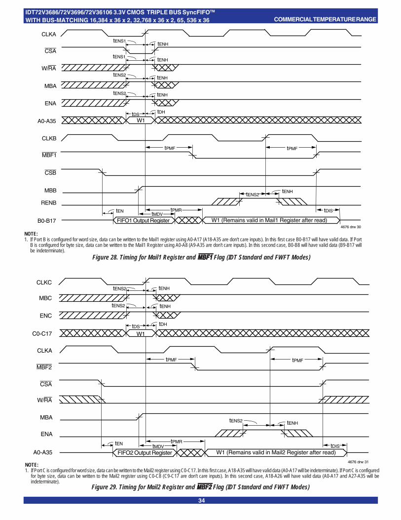
34
COMMERCIAL TEMPERATURE RANGEIDT72V3686/72V3696/72V36106 3.3V CMOS TRIPLE BUS SyncFIFOTM
WITH BUS-MATCHING 16,384 x 36 x 2, 32,768 x 36 x 2, 65, 536 x 36
Figure 28. Timing for Mail1 Register and MBF1MBF1MBF1MBF1MBF1 Flag (IDT Standard and FWFT Modes)
Figure 29. Timing for Mail2 Register and MBF2MBF2MBF2MBF2MBF2 Flag (IDT Standard and FWFT Modes)
4676 drw 30
CLKA
ENA
A0-A35
MBA
CSA
W/RA
CLKB
MBF1
CSB
MBB
RENB
B0-B17
W1
tENS1 tENH
tDS tDH
tPMF tPMF
tENS2tENH
tDIStEN tMDVtPMR
FIFO1 Output Register W1 (Remains valid in Mail1 Register after read)
tENS1 tENH
tENS2 tENH
tENS2 tENH
4676 drw 31
CLKC
ENC
C0-C17
MBC
CLKA
MBF2
CSA
MBA
ENA
A0-A35
W/RA
W1tDS tDH
tPMF tPMF
tENS2 tENH
tDIStEN tMDVtPMR
FIFO2 Output Register W1 (Remains valid in Mail2 Register after read)
tENS2 tENH
tENS2 tENH
NOTE:1. If Port C is configured for word size, data can be written to the Mail2 register using C0-C17. In this first case, A18-A35 will have valid data (A0-A17 will be indeterminate). If Port C is configured
for byte size, data can be written to the Mail2 register using C0-C8 (C9-C17 are don't care inputs). In this second case, A18-A26 will have valid data (A0-A17 and A27-A35 will beindeterminate).
NOTE:1. If Port B is configured for word size, data can be written to the Mail1 register using A0-A17 (A18-A35 are don't care inputs). In this first case B0-B17 will have valid data. If Port
B is configured for byte size, data can be written to the Mail1 Register using A0-A8 (A9-A35 are don't care inputs). In this second case, B0-B8 will have valid data (B9-B17 willbe indeterminate).
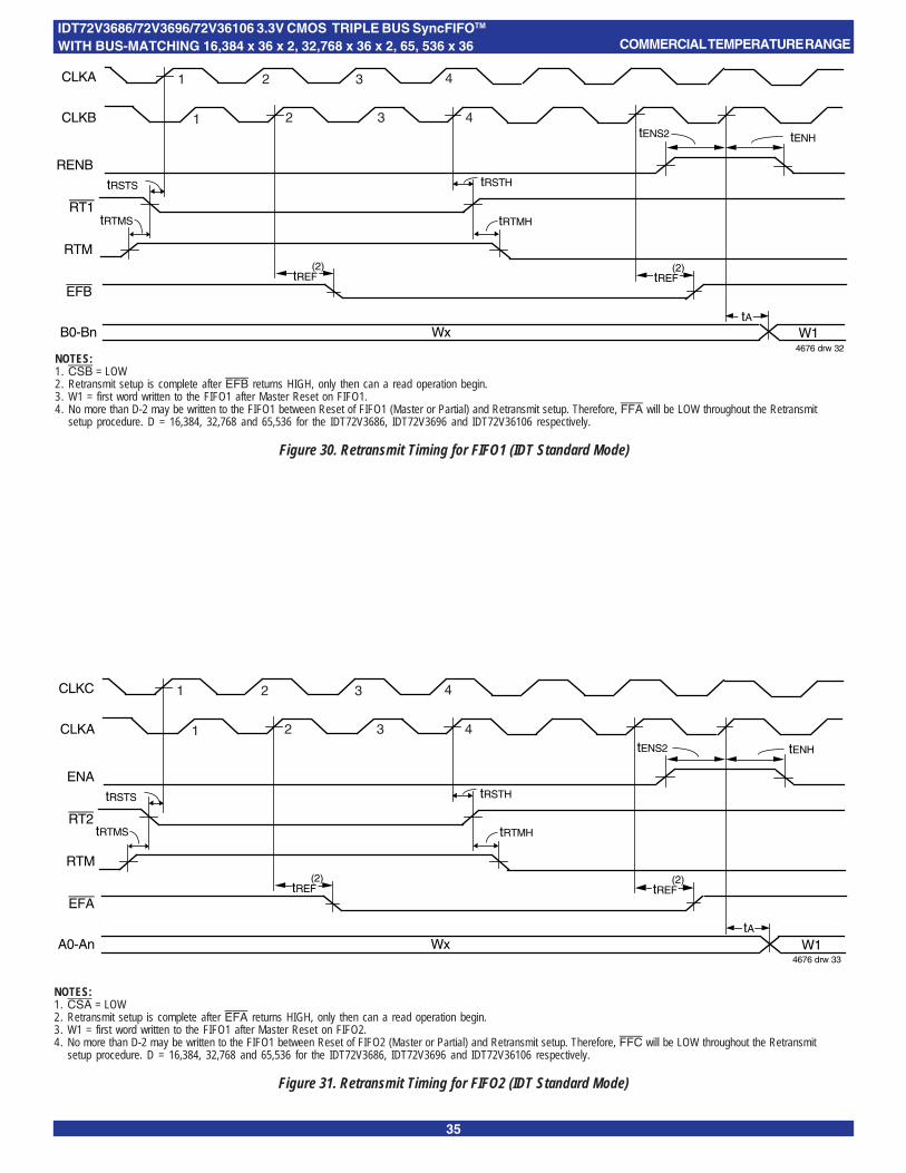
35
COMMERCIAL TEMPERATURE RANGEIDT72V3686/72V3696/72V36106 3.3V CMOS TRIPLE BUS SyncFIFOTM
WITH BUS-MATCHING 16,384 x 36 x 2, 32,768 x 36 x 2, 65, 536 x 36
CLKA
RENB
CLKB
RT1
4676 drw 32
tRSTS tRSTH
tREF(2)
B0-Bn
RTM
EFBtREF
(2)
W1WxtA
tENS2 tENH
1 3 42
1 3 42
tRTMS tRTMH
NOTES:1. CSB = LOW2. Retransmit setup is complete after EFB returns HIGH, only then can a read operation begin.3. W1 = first word written to the FIFO1 after Master Reset on FIFO1.4. No more than D-2 may be written to the FIFO1 between Reset of FIFO1 (Master or Partial) and Retransmit setup. Therefore, FFA will be LOW throughout the Retransmit
setup procedure. D = 16,384, 32,768 and 65,536 for the IDT72V3686, IDT72V3696 and IDT72V36106 respectively.
Figure 30. Retransmit Timing for FIFO1 (IDT Standard Mode)
NOTES:1. CSA = LOW2. Retransmit setup is complete after EFA returns HIGH, only then can a read operation begin.3. W1 = first word written to the FIFO1 after Master Reset on FIFO2.4. No more than D-2 may be written to the FIFO1 between Reset of FIFO2 (Master or Partial) and Retransmit setup. Therefore, FFC will be LOW throughout the Retransmit
setup procedure. D = 16,384, 32,768 and 65,536 for the IDT72V3686, IDT72V3696 and IDT72V36106 respectively.
Figure 31. Retransmit Timing for FIFO2 (IDT Standard Mode)
CLKC
ENA
CLKA
RT2
4676 drw 33
tRSTS tRSTH
tREF(2)
A0-An
RTM
EFAtREF
(2)
W1WxtA
tENS2 tENH
1 3 42
1 3 42
tRTMS tRTMH

36
COMMERCIAL TEMPERATURE RANGEIDT72V3686/72V3696/72V36106 3.3V CMOS TRIPLE BUS SyncFIFOTM
WITH BUS-MATCHING 16,384 x 36 x 2, 32,768 x 36 x 2, 65, 536 x 36
CLKA
RENB
CLKB
RT1
4676 drw 34
tRSTS tRSTH
tREF(2)
B0-Bn
RTM
ORBtREF
(2)
W1WxtA
1 3 42
1 3 42
tRTMS tRTMH
LOW
NOTES:1. CSB = LOW2. Retransmit setup is complete after ORB returns HIGH, only then can a read operation begin.3. W1 = first word written to the FIFO1 after Master Reset on FIFO1.4. No more than D-2 may be written to the FIFO1 between Reset of FIFO1 (Master or Partial) and Retransmit setup. Therefore, IRA will be LOW throughout the Retransmit
setup procedure. D = 16,385, 32,769 and 65,537 for the IDT72V3686, IDT72V3696 and IDT72V36106 respectively.
Figure 32. Retransmit Timing for FIFO1 (FWFT Mode)
CLKC
ENA
CLKA
RT2
4676 drw 35
tRSTS tRSTH
tREF(2)
A0-An
RTM
ORAtREF
(2)
W1WxtA
1 3 42
1 3 42
tRTMS tRTMH
LOW
NOTES:1. CSA = LOW2. Retransmit setup is complete after ORA returns HIGH, only then can a read operation begin.3. W1 = first word written to the FIFO2 after Master Reset on FIFO2.4. No more than D-2 may be written to the FIFO2 between Reset of FIFO2 (Master or Partial) and Retransmit setup. Therefore, IRC will be LOW throughout the Retransmit
setup procedure. D = 16,385, 32,769 and 65,537 for the IDT72V3686, IDT72V3696 and IDT72V36106 respectively.
Figure 33. Retransmit Timing for FIFO2 (FWFT Mode)

37
COMMERCIAL TEMPERATURE RANGEIDT72V3686/72V3696/72V36106 3.3V CMOS TRIPLE BUS SyncFIFOTM
WITH BUS-MATCHING 16,384 x 36 x 2, 32,768 x 36 x 2, 65, 536 x 36
4676 drw 36
CLKA
ENA
MBA
CSA
W/RA
tCLKtCLKH tCLKL
tENS2
tAtMDVtEN
tA
tENS2 tENHtENS2
tENHtENH
tDISNo Operation
Wn(1) Wn+1
LOOP
Wn-1(1)A0-A35Write to FIFO 1Write to FIFO 1
NOTES:1. Data is read from FIFO2 and written into FIFO1 & placed on Port A simultaneously. The first data word written into FIFO1 is the Previous Data Word (Wn-1)2. All FIFO status flags operate as normal, based on the contents of respective FIFO's.3. Loopback is available in both Standard IDT and FWFT modes. The diagram above is for both.
Figure 34. Loopback Operation (FIFO2 data transfer to FIFO1 and Port A)
4676 drw 37
CLKA
ENA
MBA
CSA
W/RA
tCLKtCLKH tCLKL
tENS2
tAtMDVtEN
tA
tENS2 tENHtENS2
tENHtENH
tDISNo Operation
Wn(1) Wn+1
A0-A35
LOOP
(4) WRITEto FIFO 1
HIGH-Z
Wn-1(1)
Write to FIFO 1Write to FIFO 1
NOTES:1. Data is read from FIFO2 and written into FIFO1 only. The data from FIFO2 is NOT placed on Port A. Port A is held in the high impedance state.2. All FIFO status flags operate as normal, based on the contents of respective FIFO's.3. Loopback is available in both Standard IDT and FWFT modes. The diagram above is for both.4. Write operations to FIFO1 cannot be accessed via Port A.
Figure 35. Loopback Operation (FIFO2 data transfer to FIFO1)

38
COMMERCIAL TEMPERATURE RANGEIDT72V3686/72V3696/72V36106 3.3V CMOS TRIPLE BUS SyncFIFOTM
WITH BUS-MATCHING 16,384 x 36 x 2, 32,768 x 36 x 2, 65, 536 x 36
NOTE:1. Includes probe and jig capacitance.
Figure 36. Load Circuit and Voltage Waveforms
4676 drw 38
PARAMETER MEASUREMENT INFORMATION
From OutputUnder Test
30 pF
330Ω
3.3V
510Ω
PROPAGATION DELAYLOAD CIRCUIT
3V
GND
TimingInput
Data,Enable
Input
GND
3V1.5V1.5V
VOLTAGE WAVEFORMSSETUP AND HOLD TIMES
VOLTAGE WAVEFORMSPULSE DURATIONS
VOLTAGE WAVEFORMSENABLE AND DISABLE TIMES
VOLTAGE WAVEFORMSPROPAGATION DELAY TIMES
3V
GND
GND
3V
1.5V
1.5V
1.5V
1.5V
tW
OutputEnable
Low-LevelOutput
High-LevelOutput
3V
OL
GND
3V
1.5V 1.5V
1.5V
1.5VOH
OV
GND
OH
OL
1.5V 1.5V
1.5V 1.5V
Input
In-PhaseOutput
High-LevelInput
Low-LevelInput
V
V
V
V
1.5V
3V
tS th
tPLZ
tPHZ
tPZL
tPZH tPD tPD
(1)

39
CORPORATE HEADQUARTERS for SALES: for Tech Support:6024 Silver Creek Valley Road 800-345-7015 or 408-284-8200 408-360-1753San Jose, CA 95138 fax: 408-284-2775 email: [email protected]
www.idt.com
ORDERING INFORMATION
BLANK
G
PF
1015
L
72V368672V369672V36106
Commercial (0oC to +70oC)
Green
Thin Quad Flat Pack (TQFP, PK128-1)
Low Power
16,384 x 36 x 2 ⎯ 3.3V Triple Bus SyncFIFO with Bus-Matching32,768 x 36 x 2 ⎯ 3.3V Triple Bus SyncFIFO with Bus-Matching65,536 x 36 x 2 ⎯ 3.3V Triple Bus SyncFIFO with Bus-Matching
XXXXXXDevice Type
X XX XPower Speed Package
X
Clock Cycle Time (tCLK)Speed in NanosecondsCommercial Only
Process/Temperature
Range
X
4676 drw 39
DATASHEET DOCUMENT HISTORY11/08/2000 pgs. 1, 7, 9, 10, 13, 22 and 3912/14/2000 pgs. 5 and 6.03/27/2001 pgs. 7 and 8.11/04/2003 pg. 1.05/23/2008 pgs. 1, 7, and 39.02/05/2009 pg. 39.
NOTES:1. Industrial temperature range is available by special order.2. Green parts available. For specific speeds and packages contact your sales office.