Fully Integrated, 8-ChannelUltrasound Analog Front … · fully integrated, 8-channelultrasound...
52
AFE5803 www.ti.com SLOS763A – JANUARY 2012 – REVISED JANUARY 2012 Fully Integrated, 8-Channel Ultrasound Analog Front End, 0.75 nV/rtHz, 14/12-Bit, 65 MSPS, 158 mW/CH Check for Samples: AFE5803 1FEATURES DESCRIPTION The AFE5803 is a highly integrated Analog Front-End • 8-Channel Complete Analog Front-End (AFE) solution specifically designed for ultrasound – LNA, VCAT, PGA, LPF, ADC systems in which high performance and small size • Programmable Gain Low-Noise Amplifier are required. The AFE5803 integrates a complete (LNA) time-gain-control (TGC) imaging path. It also enables users to select one of various power/noise – 24/18/12 dB Gain combinations to optimize system performance. – 0.25/0.5/1 V PP Linear Input Range Therefore, the AFE5803 is a suitable ultrasound – 0.63/0.7/0.9 nV/rtHz Input Referred Noise analog front end solution for portable systems. – Programmable Active Termination The AFE5803 contains eight channels of voltage • 40 dB Low Noise Voltage Controlled controlled amplifier (VCA), 14/12-bit Analog-to-Digital Converter (ADC). The VCA includes Low noise Attenuator (VCAT) Amplifier (LNA), Voltage controlled Attenuator • 24/30 dB Programmable Gain Amplifier (PGA) (VCAT), Programmable Gain Amplifier (PGA), and • 3 rd Order Linear Phase Low-Pass Filter (LPF) Low-Pass Filter (LPF). The LNA gain is – 10, 15, 20, 30 MHz programmable to support 250 mV PP to 1 V PP input signals. Programmable active termination is also • 14-bit Analog to Digital Converter (ADC) supported by the LNA. The ultra-low noise VCAT – 77 dBFS SNR at 65 MSPS provides an attenuation control range of 40 dB and – LVDS Outputs improves overall low gain SNR which benefits harmonic imaging and near field imaging. The PGA • Noise/Power Optimizations (Full Chain) provides gain options of 24 dB and 30 dB. Before the – 158 mW/CH at 0.75 nV/rtHz, 65 MSPS ADC, a LPF can be configured as 10 MHz, 15 MHz, – 101 mW/CH at 1.1 nV/rtHz, 40 MSPS 20 MHz or 30 MHz to support ultrasound applications with different frequencies. The high-performance • Excellent Device-to-Device Gain Matching 14bit/65 MSPS ADC in the AFE5803 achieves – ±0.5 dB (Typical) and ±0.9 dB (Max) 77dBFS SNR. It ensures excellent SNR at low chain • Low Harmonic Distortion gain. The ADC’s LVDS outputs enable flexible system integration desired for miniaturized systems. • Fast and Consistent Overload Recovery • Small Package: 15 mm x 9 mm, 135-BGA The AFE5803 is available in a 15mm × 9mm, 135-pin BGA package and it is specified for operation from 0°C to 85°C. It is also pin-to-pin compatible to the APPLICATIONS AFE5807, AFE5808 and AFE5808A. • Medical Ultrasound Imaging • Nondestructive Evaluation Equipments 1 Please be aware that an important notice concerning availability, standard warranty, and use in critical applications of Texas Instruments semiconductor products and disclaimers thereto appears at the end of this data sheet. PRODUCTION DATA information is current as of publication date. Copyright © 2012, Texas Instruments Incorporated Products conform to specifications per the terms of the Texas Instruments standard warranty. Production processing does not necessarily include testing of all parameters.
Transcript of Fully Integrated, 8-ChannelUltrasound Analog Front … · fully integrated, 8-channelultrasound...
AFE5803
www.ti.com SLOS763A –JANUARY 2012–REVISED JANUARY 2012
Fully Integrated, 8-Channel Ultrasound Analog Front End,0.75 nV/rtHz, 14/12-Bit, 65 MSPS, 158 mW/CH
Check for Samples: AFE5803
1FEATURES DESCRIPTIONThe AFE5803 is a highly integrated Analog Front-End• 8-Channel Complete Analog Front-End(AFE) solution specifically designed for ultrasound– LNA, VCAT, PGA, LPF, ADC systems in which high performance and small size
• Programmable Gain Low-Noise Amplifier are required. The AFE5803 integrates a complete(LNA) time-gain-control (TGC) imaging path. It also enables
users to select one of various power/noise– 24/18/12 dB Gaincombinations to optimize system performance.– 0.25/0.5/1 VPP Linear Input Range Therefore, the AFE5803 is a suitable ultrasound
– 0.63/0.7/0.9 nV/rtHz Input Referred Noise analog front end solution for portable systems.– Programmable Active Termination The AFE5803 contains eight channels of voltage
• 40 dB Low Noise Voltage Controlled controlled amplifier (VCA), 14/12-bit Analog-to-DigitalConverter (ADC). The VCA includes Low noiseAttenuator (VCAT)Amplifier (LNA), Voltage controlled Attenuator• 24/30 dB Programmable Gain Amplifier (PGA)(VCAT), Programmable Gain Amplifier (PGA), and
• 3rd Order Linear Phase Low-Pass Filter (LPF) Low-Pass Filter (LPF). The LNA gain is– 10, 15, 20, 30 MHz programmable to support 250 mVPP to 1 VPP input
signals. Programmable active termination is also• 14-bit Analog to Digital Converter (ADC)supported by the LNA. The ultra-low noise VCAT– 77 dBFS SNR at 65 MSPS provides an attenuation control range of 40 dB and
– LVDS Outputs improves overall low gain SNR which benefitsharmonic imaging and near field imaging. The PGA• Noise/Power Optimizations (Full Chain)provides gain options of 24 dB and 30 dB. Before the– 158 mW/CH at 0.75 nV/rtHz, 65 MSPS ADC, a LPF can be configured as 10 MHz, 15 MHz,
– 101 mW/CH at 1.1 nV/rtHz, 40 MSPS 20 MHz or 30 MHz to support ultrasound applicationswith different frequencies. The high-performance• Excellent Device-to-Device Gain Matching14bit/65 MSPS ADC in the AFE5803 achieves– ±0.5 dB (Typical) and ±0.9 dB (Max)77dBFS SNR. It ensures excellent SNR at low chain
• Low Harmonic Distortion gain. The ADC’s LVDS outputs enable flexible systemintegration desired for miniaturized systems.• Fast and Consistent Overload Recovery
• Small Package: 15 mm x 9 mm, 135-BGA The AFE5803 is available in a 15mm × 9mm, 135-pinBGA package and it is specified for operation from0°C to 85°C. It is also pin-to-pin compatible to theAPPLICATIONSAFE5807, AFE5808 and AFE5808A.• Medical Ultrasound Imaging
• Nondestructive Evaluation Equipments
1
Please be aware that an important notice concerning availability, standard warranty, and use in critical applications of TexasInstruments semiconductor products and disclaimers thereto appears at the end of this data sheet.
PRODUCTION DATA information is current as of publication date. Copyright © 2012, Texas Instruments IncorporatedProducts conform to specifications per the terms of the TexasInstruments standard warranty. Production processing does notnecessarily include testing of all parameters.
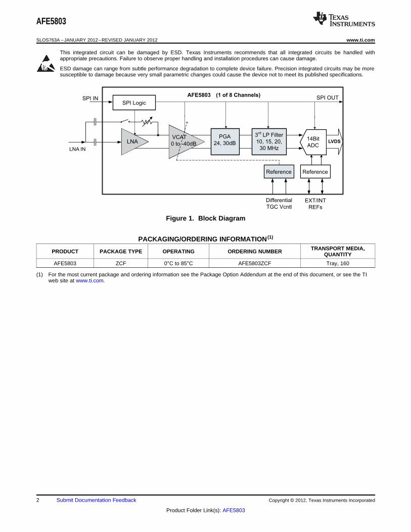
SPI IN
LNA 0 to -40dB
SPI Logic
LNA IN
PGA
24, 30dB
3rd
LP Filter
10, 15, 20,
30 MHz
AFE5803 (1 of 8 Channels)
14Bit
ADCLVDS
ReferenceReference
Differential
TGC VcntlEXT/INT
REFs
SPI OUT
VCAT
AFE5803
SLOS763A –JANUARY 2012–REVISED JANUARY 2012 www.ti.com
This integrated circuit can be damaged by ESD. Texas Instruments recommends that all integrated circuits be handled withappropriate precautions. Failure to observe proper handling and installation procedures can cause damage.
ESD damage can range from subtle performance degradation to complete device failure. Precision integrated circuits may be moresusceptible to damage because very small parametric changes could cause the device not to meet its published specifications.
Figure 1. Block Diagram
PACKAGING/ORDERING INFORMATION (1)
TRANSPORT MEDIA,PRODUCT PACKAGE TYPE OPERATING ORDERING NUMBER QUANTITY
AFE5803 ZCF 0°C to 85°C AFE5803ZCF Tray, 160
(1) For the most current package and ordering information see the Package Option Addendum at the end of this document, or see the TIweb site at www.ti.com.
2 Submit Documentation Feedback Copyright © 2012, Texas Instruments Incorporated
Product Folder Link(s): AFE5803

AFE5803
www.ti.com SLOS763A –JANUARY 2012–REVISED JANUARY 2012
ABSOLUTE MAXIMUM RATINGSover operating free-air temperature range (unless otherwise noted) (1)
VALUE UNIT
MIN MAX
AVDD –0.3 3.9 V
AVDD_ADC –0.3 2.2 VSupply voltagerange AVDD_5V –0.3 6 V
DVDD –0.3 2.2 V
Voltage between AVSS and LVSS –0.3 0.3 V
Voltage at analog inputs and digital inputs –0.3 min [3.6,AVDD+0.3] V
Peak solder temperature (2) 260 °CMaximum junction temperature (TJ), any condition 105 °CStorage temperature range –55 150 °COperating temperature range 0 85 °C
Human Body Model (HBM) 2000 VESD Ratings
Charged Device Model (CDM) 500 V
(1) Stresses above those listed under absolute maximum ratings may cause permanent damage to the device. These are stress ratingsonly and functional operation of the device at these or any other conditions beyond those indicated under "recommended operatingconditions" is not implied Exposure to absolute maximum rated conditions for extended periods may degrade device reliability.
(2) Device complies with JSTD-020D.
THERMAL INFORMATIONAFE5803
THERMAL METRIC (1) BGA UNITS
135 PINS
θJA Junction-to-ambient thermal resistance 34.1
θJCtop Junction-to-case (top) thermal resistance 5
θJB Junction-to-board thermal resistance 11.5°C/W
ψJT Junction-to-top characterization parameter 0.2
ψJB Junction-to-board characterization parameter 10.8
θJCbot Junction-to-case (bottom) thermal resistance n/a
(1) For more information about traditional and new thermal metrics, see the IC Package Thermal Metrics application report, SPRA953.
RECOMMENDED OPERATING CONDITIONSPARAMETER MIN MAX UNIT
AVDD 3.15 3.6 V
AVDD_ADC 1.7 1.9 V
DVDD 1.7 1.9 V
AVDD_5V 4.75 5.5 V
Ambient Temperature, TA 0 85 °C
Copyright © 2012, Texas Instruments Incorporated Submit Documentation Feedback 3
Product Folder Link(s): AFE5803

AFE5803
SLOS763A –JANUARY 2012–REVISED JANUARY 2012 www.ti.com
DEVICE INFORMATION
PIN CONFIGURATIONTop View
ZCF (BGA-135)1 2 3 4 5 6 7 8 9
A AVDD INP8 INP7 INP6 INP5 INP4 INP3 INP2 INP1
B CM_BYP ACT8 ACT7 ACT6 ACT5 ACT4 ACT3 ACT2 ACT1
C AVSS INM8 INM7 INM6 INM5 INM4 INM3 INM2 INM1
D AVSS AVSS AVSS AVSS AVSS AVSS AVSS AVDD AVDD
E CH7_TEST_OUTP CH7_TEST_OUTM AVSS AVSS AVSS AVSS AVSS AVDD AVDD
F CH7_BUFFER_OUTM CH7_BUFFER_OUTP AVSS AVSS AVSS AVSS AVSS DNC DNC
G AVSS AVSS AVSS AVSS AVSS AVSS AVSS DNC DNC
H CH8_BUFFER_OUTM CH8_BUFFER_OUTP AVSS AVSS AVSS AVSS AVSS PDN_GLOBAL RESET
J CH8_TEST_OUTP CH8_TEST_OUTM AVSS AVSS AVSS AVDD_ADC AVDD_ADC PDN_VCA SCLK
K AVDD AVDD_5V VCNTLP VCNTLM VHIGH AVSS DNC AVDD_ADC SDATA
L CLKP_ADC CLKM_ADC AVDD_ADC REFM DNC DNC DNC PDN_ADC SEN
M AVDD_ADC AVDD_ADC VREF_IN REFP DNC DNC DNC DNC SDOUT
N D8P D8M DVDD DNC DVSS DNC DVDD D1M D1P
P D7M D6M D5M FCLKM DVSS DCLKM D4M D3M D2M
R D7P D6P D5P FCLKP DVSS DCLKP D4P D3P D2P
PIN FUNCTIONSPIN
DESCRIPTIONNO. NAME
B9~ B2 ACT1...ACT8 Active termination input pins for CH1~8. 1 μF capacitors are recommended. See the ApplicaitonInformation section.
A1, D8, D9, E8, AVDD 3.3 V Analog supply for LNA, VCAT, PGA, LPF blocks.E9, K1
K2 AVDD_5V 5 V Analog supply for LNA, VCAT, PGA, LPF blocks.
J6, J7, K8, L3, AVDD_ADC 1.8 V Analog power supply for ADC.M1, M2
C1, D1~D7,E3~E7, F3~F7,G1~G7, AVSS Analog ground.H3~H7,J3~J5,K6
Negative input of differential ADC clock. In the single-end clock mode, it can be tied to GND directly orL2 CLKM_ADC through a 0.1 µF capacitor.
Positive input of differential ADC clock. In the single-end clock mode, it can be tied to clock signalL1 CLKP_ADC directly or through a 0.1 µF capacitor.
Bias voltage and bypass to ground. ≥1µF is recommended. To suppress the ultra low frequency noise,B1 CM_BYP 10µF can be used.
E2 CH7_TEST_OUTM CH7 PGA negative output when PGA test mode is enabled. Can be floated if not used.
E1 CH7_TEST_OUTP CH7 PGA positive output when PGA test mode is enabled. Can be floated if not used.
Negative differential output for the buffer amplifier when PGA test mode is enabled. Can be floated if notF1 CH7_BUFFER_OUTM used. See the TEST MODES in the application information section.
Positive differential output for the buffer amplifier when PGA test mode is enabled. Can be floated if notF2 CH7_BUFFER_OUTP used. See the TEST MODES in the application information section.
J2 CH8_TEST_OUTM CH8 PGA negative output when PGA test mode is enabled. Can be floated if not used.
J1 CH8_TEST_OUTP CH8 PGA positive output when PGA test mode is enabled. Can be floated if not used.
Negative differential output for the buffer amplifier when PGA test mode is enabled. Can be floated if notH1 CH8_BUFFER_OUTM used. See the TEST MODES in the application information section.
Positive differential output for the buffer amplifier when PGA test mode is enabled. Can be floated if notH2 CH8_BUFFER_OUTP used. See the TEST MODES in the application information section.
N8, P9~P7, D1M~D8M ADC CH1~8 LVDS negative outputsP3~P1, N2
N9, R9~R7, D1P~D8P ADC CH1~8 LVDS positive outputsR3~R1, N1
P6 DCLKM LVDS bit clock (7x) negative output
4 Submit Documentation Feedback Copyright © 2012, Texas Instruments Incorporated
Product Folder Link(s): AFE5803
AFE5803
www.ti.com SLOS763A –JANUARY 2012–REVISED JANUARY 2012
PIN FUNCTIONS (continued)PIN
DESCRIPTIONNO. NAME
R6 DCLKP LVDS bit clock (7x) positive output
F8, F9, G8, G9,K7, DNC Do not connect. Must leave floatedL5~L7,M5~M8,N4, N6
N3, N7 DVDD ADC digital and I/O power supply, 1.8 V
N5, P5, R5 DVSS ADC digital ground
P4 FCLKM LVDS frame clock (1X) negative output
R4 FCLKP LVDS frame clock (1X) positive output
CH1~8 complimentary analog inputs. Bypass to ground with ≥ 0.015 µF capacitors. The HPF responseC9~C2 INM1…INM8 of the LNA depends on the capacitors.
A9~A2 INP1...INP8 CH1~8 analog inputs. AC couple to inputs with ≥ 0.1µF capacitors.
L8 PDN_ADC ADC partial (fast) power down control pin with an internal pull down resistor of 100 kΩ. Active High.
J8 PDN_VCA VCA partial (fast) power down control pin with an internal pull down resistor of 20 kΩ. Active High.
Global (complete) power-down control pin for the entire chip with an internal pull down resistor of 20kΩ.H8 PDN_GLOBAL Active High.
0.5 V reference output in the internal reference mode. Must leave floated in the internal reference mode.L4 REFM Adding test point on PCB is recommended for monitoring the reference output.
1.5 V reference output in the internal reference mode. Must leave floated in the internal reference mode.M4 REFP Adding test point on PCB is recommended for monitoring the reference output.
H9 RESET Hardware reset pin with an internal pull-down resistor of 20 kΩ. Active high.
J9 SCLK Serial interface clock input with an internal pull-down resistor of 2 0kΩ
K9 SDATA Serial interface data input with an internal pull-down resistor of 20 kΩ
M9 SDOUT Serial interface data readout. High impedance when readout is disabled.
L9 SEN Serial interface enable with an internal pull up resistor of 20 kΩ. Active low.
K4 VCNTLM Negative differential attenuation control pin.
K3 VCNTLP Positive differential attenuation control pin
K5 VHIGH Bias voltage; bypass to ground with ≥1µF.
M3 VREF_IN ADC 1.4 V reference input in the external reference mode; bypass to ground with 0. 1 µF.
F8, F9, G8, G9,K7, L5~L7, DNC Do not connect. Must leave floatedM5~M8, N4,N6
Copyright © 2012, Texas Instruments Incorporated Submit Documentation Feedback 5
Product Folder Link(s): AFE5803
u
8CH_SNR-
10N 10 1 1C= x -
1CH_SNRN + N 56 7-C
1010
AFE5803
SLOS763A –JANUARY 2012–REVISED JANUARY 2012 www.ti.com
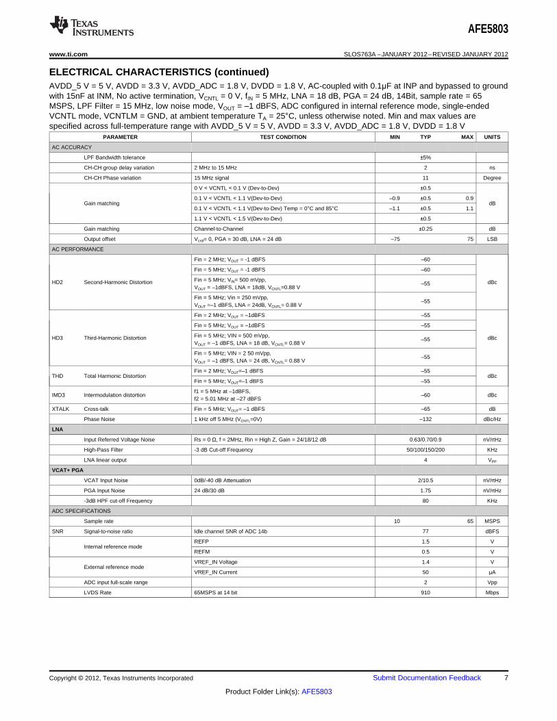
ELECTRICAL CHARACTERISTICSAVDD_5 V = 5 V, AVDD = 3.3 V, AVDD_ADC = 1.8 V, DVDD = 1.8 V, AC-coupled with 0.1µF at INP and bypassed to groundwith 15nF at INM, No active termination, VCNTL = 0 V, fIN = 5 MHz, LNA = 18 dB, PGA = 24 dB, 14Bit, sample rate = 65MSPS, LPF Filter = 15 MHz, low noise mode, VOUT = –1 dBFS, ADC configured in internal reference mode, single-endedVCNTL mode, VCNTLM = GND, at ambient temperature TA = 25°C, unless otherwise noted. Min and max values arespecified across full-temperature range with AVDD_5 V = 5 V, AVDD = 3.3 V, AVDD_ADC = 1.8 V, DVDD = 1.8 V
PARAMETER TEST CONDITION MIN TYP MAX UNITS
TGC FULL SIGNAL CHANNEL (LNA+VCAT+LPF+ADC)
Rs = 0 Ω, f = 2 MHz, LNA =24/18/12 dB, PGA = 2 4dB 0.76/0.83/1.16Input voltage noise over LNA Gain(lownV/rtHz
noise mode) Rs = 0 Ω, f = 2 MHz,LNA =24/18/12 dB, PGA = 30 dB 0.75/0.86/1.12
Rs = 0 Ω, f = 2 MHz,LNA =24/18/12 dB, PGA = 24 dB 1.1/1.2/1.45Input voltage noise over LNA Gain(lowen (RTI) nV/rtHz
power mode) Rs = 0 Ω, f = 2 MHz, LNA =24/18/12 dB, PGA = 30 dB 1.1/1.2/1.45
Rs = 0 Ω, f = 2 MHz,LNA = 24/18/12 dB, PGA = 24 dB 1/1.05/1.25Input Voltage Noise over LNAnV/rtHz
Gain(Medium Power Mode) Rs = 0 Ω, f = 2 MHz, LNA = 24/18/12 dB, PGA = 30 dB 0.95/1.0/1.2
Input referred current noise Low Noise Mode/Medium Power Mode/Low Power Mode 2.7/2.1/2 pA/rtHz
Rs = 200 Ω, 200 Ω active termination, PGA = 24dB,LNA = 12/18/24 dB 3.85/2.4/1.8 dBNF Noise figure
Rs = 100 Ω, 100 Ω active termination, PGA = 24dB,LNA = 12/18/24 dB 5.3/3.1/2.3 dB
VMAX Maximum Linear Input Voltage LNA gain = 24/18/12 dB 250/500/1000mVPP
VCLAMP Clamp Voltage Reg52[10:9] = 0, LNA = 24/18/12 dB 350/600/1150
Low noise mode 24/30PGA Gain dB
Medium/Low power mode 24/28.5
LNA = 24 dB, PGA = 30 dB, Low noise mode 54
Total gain LNA = 2 4dB, PGA = 30 dB, Med power mode 52.5 dB
LNA = 24 dB, PGA = 30 dB, Low power mode 52.5
Ch-CH Noise Correlation Factor withoutSumming of 8 channels 0
Signal (1)
Full band (VCNTL = 0/0.8) 0.15/0.17Ch-CH Noise Correlation Factor withSignal (1)
1MHz band over carrier (VCNTL= 0/0.8) 0.18/0.75
VCNTL = 0.6V(22 dB total channel gain) 68 70
Signal to Noise Ratio (SNR) VCNTL = 0, LNA = 18 dB, PGA =24 dB 59.3 63 dBFS
VCNTL = 0, LNA = 24 dB, PGA = 24 dB 58
SNR over 2 MHz band around carrier at VCNTL = 0.6 V ( 22 dB totalNarrow Band SNR 75 77 dBFS
gain)
Input Common-mode Voltage At INP and INM pins 2.4 V
8 kΩInput resistance
Preset active termination enabled 50/100/200/400 Ω
Input capacitance 20 pF
Input Control Voltage VCNTLP - VCNTLM 0 1.5 V
Common-mode voltage VCNTLP and VCNTLM 0.75 V
Gain Range -40 dB
Gain Slope VCNTL= 0.1 V to 1.1 V 35 dB/V
Input Resistance Between VCNTLP and VCNTLM 200 KΩ
Input Capacitance Between VCNTLP and VCNTLM 1 pF
TGC Response Time VCNT L= 0 V to 1.5 V step function 1.5 µs
3rd order-Low-pass Filter 10, 15, 20, 30 MHz
Settling time for change in LNA gain 14 µs
Settling time for change in active1 µs
termination setting
(1) Noise correlation factor is defined as Nc/(Nu+Nc), where Nc is the correlated noise power in single channel; and Nu is the uncorrelatednoise power in single channel. Its measurement follows the below equation, in which the SNR of single channel signal and the SNR ofsummed eight channel signal are measured.
6 Submit Documentation Feedback Copyright © 2012, Texas Instruments Incorporated
Product Folder Link(s): AFE5803
AFE5803
www.ti.com SLOS763A –JANUARY 2012–REVISED JANUARY 2012
ELECTRICAL CHARACTERISTICS (continued)AVDD_5 V = 5 V, AVDD = 3.3 V, AVDD_ADC = 1.8 V, DVDD = 1.8 V, AC-coupled with 0.1µF at INP and bypassed to groundwith 15nF at INM, No active termination, VCNTL = 0 V, fIN = 5 MHz, LNA = 18 dB, PGA = 24 dB, 14Bit, sample rate = 65MSPS, LPF Filter = 15 MHz, low noise mode, VOUT = –1 dBFS, ADC configured in internal reference mode, single-endedVCNTL mode, VCNTLM = GND, at ambient temperature TA = 25°C, unless otherwise noted. Min and max values arespecified across full-temperature range with AVDD_5 V = 5 V, AVDD = 3.3 V, AVDD_ADC = 1.8 V, DVDD = 1.8 V
PARAMETER TEST CONDITION MIN TYP MAX UNITS
AC ACCURACY
LPF Bandwidth tolerance ±5%
CH-CH group delay variation 2 MHz to 15 MHz 2 ns
CH-CH Phase variation 15 MHz signal 11 Degree
0 V < VCNTL < 0.1 V (Dev-to-Dev) ±0.5
0.1 V < VCNTL < 1.1 V(Dev-to-Dev) –0.9 ±0.5 0.9Gain matching dB
0.1 V < VCNTL < 1.1 V(Dev-to-Dev) Temp = 0°C and 85°C –1.1 ±0.5 1.1
1.1 V < VCNTL < 1.5 V(Dev-to-Dev) ±0.5
Gain matching Channel-to-Channel ±0.25 dB
Output offset Vcntl= 0, PGA = 30 dB, LNA = 24 dB –75 75 LSB
AC PERFORMANCE
Fin = 2 MHz; VOUT = -1 dBFS –60
Fin = 5 MHz; VOUT = -1 dBFS –60
Fin = 5 MHz; VIN= 500 mVpp,HD2 Second-Harmonic Distortion dBc–55VOUT = –1dBFS, LNA = 18dB, VCNTL=0.88 V
Fin = 5 MHz; Vin = 250 mVpp,–55
VOUT =–1 dBFS, LNA = 24dB, VCNTL= 0.88 V
Fin = 2 MHz; VOUT = –1dBFS –55
Fin = 5 MHz; VOUT = –1dBFS –55
Fin = 5 MHz; VIN = 500 mVpp,HD3 Third-Harmonic Distortion dBc–55VOUT = –1 dBFS, LNA = 18 dB, VCNTL= 0.88 V
Fin = 5 MHz; VIN = 2 50 mVpp,–55
VOUT = –1 dBFS, LNA = 24 dB, VCNTL= 0.88 V
Fin = 2 MHz; VOUT=–1 dBFS –55THD Total Harmonic Distortion dBc
Fin = 5 MHz; VOUT=–1 dBFS –55
f1 = 5 MHz at –1dBFS,IMD3 Intermodulation distortion –60 dBc
f2 = 5.01 MHz at –27 dBFS
XTALK Cross-talk Fin = 5 MHz; VOUT= –1 dBFS –65 dB
Phase Noise 1 kHz off 5 MHz (VCNTL=0V) –132 dBc/Hz
LNA
Input Referred Voltage Noise Rs = 0 Ω, f = 2MHz, Rin = High Z, Gain = 24/18/12 dB 0.63/0.70/0.9 nV/rtHz
High-Pass Filter -3 dB Cut-off Frequency 50/100/150/200 KHz
LNA linear output 4 VPP
VCAT+ PGA
VCAT Input Noise 0dB/-40 dB Attenuation 2/10.5 nV/rtHz
PGA Input Noise 24 dB/30 dB 1.75 nV/rtHz
-3dB HPF cut-off Frequency 80 KHz
ADC SPECIFICATIONS
Sample rate 10 65 MSPS
SNR Signal-to-noise ratio Idle channel SNR of ADC 14b 77 dBFS
REFP 1.5 VInternal reference mode
REFM 0.5 V
VREF_IN Voltage 1.4 VExternal reference mode
VREF_IN Current 50 µA
ADC input full-scale range 2 Vpp
LVDS Rate 65MSPS at 14 bit 910 Mbps
Copyright © 2012, Texas Instruments Incorporated Submit Documentation Feedback 7
Product Folder Link(s): AFE5803

AFE5803
SLOS763A –JANUARY 2012–REVISED JANUARY 2012 www.ti.com
ELECTRICAL CHARACTERISTICS (continued)AVDD_5 V = 5 V, AVDD = 3.3 V, AVDD_ADC = 1.8 V, DVDD = 1.8 V, AC-coupled with 0.1µF at INP and bypassed to groundwith 15nF at INM, No active termination, VCNTL = 0 V, fIN = 5 MHz, LNA = 18 dB, PGA = 24 dB, 14Bit, sample rate = 65MSPS, LPF Filter = 15 MHz, low noise mode, VOUT = –1 dBFS, ADC configured in internal reference mode, single-endedVCNTL mode, VCNTLM = GND, at ambient temperature TA = 25°C, unless otherwise noted. Min and max values arespecified across full-temperature range with AVDD_5 V = 5 V, AVDD = 3.3 V, AVDD_ADC = 1.8 V, DVDD = 1.8 V
PARAMETER TEST CONDITION MIN TYP MAX UNITS
POWER DISSIPATION
AVDD Voltage 3.15 3.3 3.6 V
AVDD_ADC Voltage 1.7 1.8 1.9 V
AVDD_5V Voltage 4.75 5 5.5 V
DVDD Voltage 1.7 1.8 1.9 V
TGC low noise mode, 65 MSPS 158 190
TGC low noise mode, 40 MSPS 145Total power dissipation per channel mW/CH
TGC medium power mode, 40 MSPS 114
TGC low power mode, 40 MSPS 101.5
TGC low noise mode, no signal 202 240
TGC medium power mode, no signal 126
TGC low power mode, no signal 99AVDD (3.3V) Current mA
TGC low noise mode, 500 mVPP Input,1% duty cycle 210
TGC medium power mode, 500 mVPP Input, 1% duty cycle 133
TGC low power, 500 mVPP Input, 1% duty cycle 105
TGC mode no signal 25.5 35AVDD_5V Current mA
TGC mode, 500 mVPP Input,1% duty cycle 16.5
TGC low noise mode, no signal 99 121
TGC medium power mode, no signal 68
TGC low power mode, no signal 55.5VCA Power dissipation mW/CH
TGC low noise mode, 500 mVPP input,1% duty cycle 102.5
TGC medium power mode, 500 mVPP Input, 1% duty cycle 71
TGC low power mode, 500 mVPP input,1% duty cycle 59.5
AVDD_ADC(1.8V) Current 65 MSPS 187 205 mA
DVDD(1.8V) Current 65 MSPS 77 110 mA
65 MSPS 59 69
50 MSPS 51ADC Power dissipation/CH mW/CH
40 MSPS 46
20 MSPS 35
Power dissipation in power down mode PDN_VCA = High, PDN_ADC = High 25 mW/CH
Complete power-down PDN_Global=High 0.6
Power-down response time Time taken to enter power down 1 µs
Power-up response time VCA power down 2µs+1% of PDNtime µs
ADC power down 1
Complete power down 2.5 ms
fin = 5 MHz, at 50 mVpp noise at 1 KHz on supply (2) –65 dBcPower supply modulation ratio, AVDD andAVDD_5V fin = 5 MHz, at 50 mVpp noise at 50 KHz on supply(2) –65 dBc
Power supply rejection ratio f = 10 kHz,VCNTL = 0 V (high gain), AVDD –40 dBc
f = 10 kHz,VCNTL = 0 V(high gain), AVDD_5V –55 dBc
f = 10 kHz,VCNTL = 1 V (low gain), AVDD –50 dBc
(2) PSMR specification is with respect to input signal amplitude.
8 Submit Documentation Feedback Copyright © 2012, Texas Instruments Incorporated
Product Folder Link(s): AFE5803
AFE5803
www.ti.com SLOS763A –JANUARY 2012–REVISED JANUARY 2012
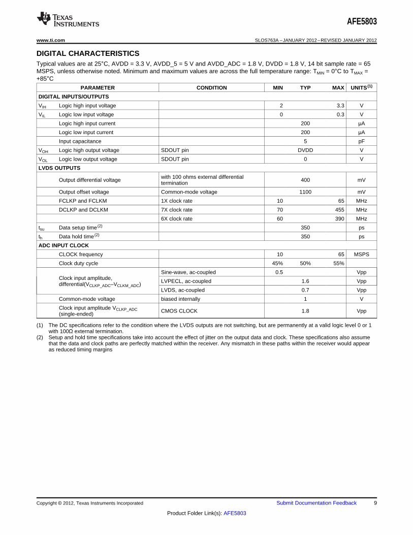
DIGITAL CHARACTERISTICSTypical values are at 25°C, AVDD = 3.3 V, AVDD_5 = 5 V and AVDD_ADC = 1.8 V, DVDD = 1.8 V, 14 bit sample rate = 65MSPS, unless otherwise noted. Minimum and maximum values are across the full temperature range: TMIN = 0°C to TMAX =+85°C
PARAMETER CONDITION MIN TYP MAX UNITS (1)
DIGITAL INPUTS/OUTPUTS
VIH Logic high input voltage 2 3.3 V
VIL Logic low input voltage 0 0.3 V
Logic high input current 200 µA
Logic low input current 200 µA
Input capacitance 5 pF
VOH Logic high output voltage SDOUT pin DVDD V
VOL Logic low output voltage SDOUT pin 0 V
LVDS OUTPUTS
with 100 ohms external differentialOutput differential voltage 400 mVtermination
Output offset voltage Common-mode voltage 1100 mV
FCLKP and FCLKM 1X clock rate 10 65 MHz
DCLKP and DCLKM 7X clock rate 70 455 MHz
6X clock rate 60 390 MHz
tsu Data setup time (2) 350 ps
th Data hold time (2) 350 ps
ADC INPUT CLOCK
CLOCK frequency 10 65 MSPS
Clock duty cycle 45% 50% 55%
Sine-wave, ac-coupled 0.5 VppClock input amplitude, LVPECL, ac-coupled 1.6 Vppdifferential(VCLKP_ADC–VCLKM_ADC)
LVDS, ac-coupled 0.7 Vpp
Common-mode voltage biased internally 1 V
Clock input amplitude VCLKP_ADC CMOS CLOCK 1.8 Vpp(single-ended)
(1) The DC specifications refer to the condition where the LVDS outputs are not switching, but are permanently at a valid logic level 0 or 1with 100Ω external termination.
(2) Setup and hold time specifications take into account the effect of jitter on the output data and clock. These specifications also assumethat the data and clock paths are perfectly matched within the receiver. Any mismatch in these paths within the receiver would appearas reduced timing margins
Copyright © 2012, Texas Instruments Incorporated Submit Documentation Feedback 9
Product Folder Link(s): AFE5803

0
5
10
15
20
25
30
35
40
45
0.0 0.1 0.2 0.3 0.4 0.5 0.6 0.7 0.8 0.9 1.0 1.1 1.2 1.3 1.4 1.5Vcntl (V)
Gai
n (d
B)
Low noiseMedium powerLow power
0
5
10
15
20
25
30
35
40
45
0.0 0.1 0.2 0.3 0.4 0.5 0.6 0.7 0.8 0.9 1.0 1.1 1.2Vcntl (V)
Gai
n (d
B)
−40 deg C25 deg C85 deg C
−0.
9
−0.
8
−0.
7
−0.
6
−0.
5
−0.
4
−0.
3
−0.
2
−0.
1 0
0.1
0.2
0.3
0.4
0.5
−0.
9
−0.
8
−0.
7
−0.
6
−0.
5
−0.
4
−0.
3
−0.
2
−0.
1 0
0.1
0.2
0.3
0.4
0.5
0
1000
2000
3000
4000
5000
6000
7000
8000
9000
Gain (dB)
Num
ber
of O
ccur
renc
es
G004
−0.
7
−0.
6
−0.
5
−0.
4
−0.
3
−0.
2
−0.
1 0
0.1
0.2
0.3
0.4
0.5
0.6
−0.
7
−0.
6
−0.
5
−0.
4
−0.
3
−0.
2
−0.
1 0
0.1
0.2
0.3
0.4
0.5
0.6
0
1000
2000
3000
4000
5000
6000
7000
8000
9000
Gain (dB)
Num
ber
of O
ccur
renc
es
G005
−0.
7
−0.
6
−0.
5
−0.
4
−0.
3
−0.
2
−0.
1 0
0.1
0.2
0.3
0.4
0.5
0.6
0.7
−0.
7
−0.
6
−0.
5
−0.
4
−0.
3
−0.
2
−0.
1 0
0.1
0.2
0.3
0.4
0.5
0.6
0.7
0
1000
2000
3000
4000
5000
6000
7000
8000
Gain (dB)
Num
ber
of O
ccur
renc
es
G005
−72
−68
−64
−60
−56
−52
−48
−44
−40
−36
−32
−28
−24
−20
−16
−12 −
8−
4 0 4 8 12 16 20 24 28 32 36 40 44 48 52 56 60 64 68
−72
−68
−64
−60
−56
−52
−48
−44
−40
−36
−32
−28
−24
−20
−16
−12 −
8−
4 0 4 8 12 16 20 24 28 32 36 40 44 48 52 56 60 64 68
0
10
20
30
40
50
60
70
80
90
100
110
120
ADC Output
Num
ber
of O
ccur
renc
es
G058
AFE5803
SLOS763A –JANUARY 2012–REVISED JANUARY 2012 www.ti.com
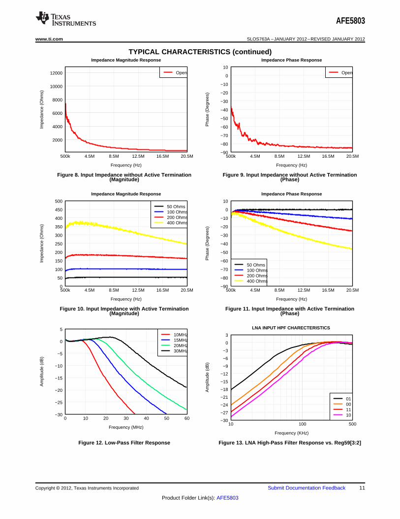
TYPICAL CHARACTERISTICS
AVDD_5 V = 5 V, AVDD = 3.3 V, AVDD_ADC = 1.8 V, DVDD = 1.8 V, ac-coupled with 0.1µF caps at INP and 15nF caps at INM, No active termination, VCNTL = 0 V, FIN = 5 MHz, LNA = 18 dB, PGA = 24 dB, 14 Bit, samplerate = 65 MSPS, LPF Filter = 15 MHz, low noise mode, VOUT = -1dBFS, ADC is configured in internal referencemode, single-ended VCNTL mode, VCNTLM = GND, at ambient temperature TA = 25°C, unless otherwise noted.
Figure 2. Gain vs. VCNTL, LNA = 18 dB and PGA = 24 dB Figure 3. Gain Variation vs. Temperature, LNA = 18 dB andPGA = 24 dB
Figure 4. Gain Matching Histogram, Figure 5. Gain Matching Histogram,VCNTL= 0.3V (34951 channels) VCNTL = 0.6V (34951 channels)
Figure 6. Gain Matching Histogram, Figure 7. Output Offset Histogram, VCNTL = 0V (1247channels)VCNTL = 0.9V (34951 channels)
10 Submit Documentation Feedback Copyright © 2012, Texas Instruments Incorporated
Product Folder Link(s): AFE5803
2000
4000
6000
8000
10000
12000
500k 4.5M 8.5M 12.5M 16.5M 20.5M
Impedance Magnitude Response
Frequency (Hz)
Impe
danc
e (O
hms)
Open
−90
−80
−70
−60
−50
−40
−30
−20
−10
0
10
500k 4.5M 8.5M 12.5M 16.5M 20.5M
Impedance Phase Response
Frequency (Hz)
Pha
se (
Deg
rees
)
Open
0
50
100
150
200
250
300
350
400
450
500
500k 4.5M 8.5M 12.5M 16.5M 20.5M
Impedance Magnitude Response
Frequency (Hz)
Impe
danc
e (O
hms)
50 Ohms100 Ohms200 Ohms400 Ohms
−90
−80
−70
−60
−50
−40
−30
−20
−10
0
10
500k 4.5M 8.5M 12.5M 16.5M 20.5M
Impedance Phase Response
Frequency (Hz)
Pha
se (
Deg
rees
)
50 Ohms100 Ohms200 Ohms400 Ohms
−30
−25
−20
−15
−10
−5
0
5
0 10 20 30 40 50 60
Frequency (MHz)
Am
plitu
de (
dB)
10MHz15MHz20MHz30MHz
−30
−27
−24
−21
−18
−15
−12
−9
−6
−3
0
3
10 100 500
LNA INPUT HPF CHARECTERISTICS
Frequency (KHz)
Am
plitu
de (
dB)
01001110
AFE5803
www.ti.com SLOS763A –JANUARY 2012–REVISED JANUARY 2012
TYPICAL CHARACTERISTICS (continued)
Figure 8. Input Impedance without Active Termination Figure 9. Input Impedance without Active Termination(Magnitude) (Phase)
Figure 10. Input Impedance with Active Termination Figure 11. Input Impedance with Active Termination(Magnitude) (Phase)
Figure 12. Low-Pass Filter Response Figure 13. LNA High-Pass Filter Response vs. Reg59[3:2]
Copyright © 2012, Texas Instruments Incorporated Submit Documentation Feedback 11
Product Folder Link(s): AFE5803
0
10
20
30
40
50
60
0.0 0.1 0.2 0.3 0.4 0.5 0.6 0.7 0.8 0.9 1.0 1.1 1.2Vcntl (V)
Inpu
t ref
fere
d no
ise
(nV
Hz
)
LNA 12 dBLNA 18 dBLNA 24 dB
−40
−35
−30
−25
−20
−15
−10
−5
0
5
10 100 500
HPF CHARECTERISTICS (LNA+VCA+PGA+ADC)
Frequency (KHz)
Am
plitu
de (
dB)
0.0
0.5
1.0
1.5
2.0
2.5
3.0
3.5
0.0 0.1 0.2 0.3 0.4Vcntl (V)
Inpu
t ref
fere
d no
ise
(nV
Hz
)
LNA 12 dBLNA 18 dBLNA 24 dB
0
10
20
30
40
50
60
70
0.0 0.1 0.2 0.3 0.4 0.5 0.6 0.7 0.8 0.9 1.0 1.1 1.2Vcntl (V)
Inpu
t ref
fere
d no
ise
(nV
Hz
)
LNA 12 dBLNA 18 dBLNA 24 dB
0.5
1.0
1.5
2.0
2.5
3.0
3.5
4.0
0.0 0.1 0.2 0.3 0.4Vcntl (V)
Inpu
t ref
fere
d no
ise
(nV
Hz
)
LNA 12 dBLNA 18 dBLNA 24 dB
0
10
20
30
40
50
60
70
0.0 0.1 0.2 0.3 0.4 0.5 0.6 0.7 0.8 0.9 1.0 1.1 1.2Vcntl (V)
Inpu
t ref
fere
d no
ise
(nV
Hz
)
LNA 12 dBLNA 18 dBLNA 24 dB
AFE5803
SLOS763A –JANUARY 2012–REVISED JANUARY 2012 www.ti.com
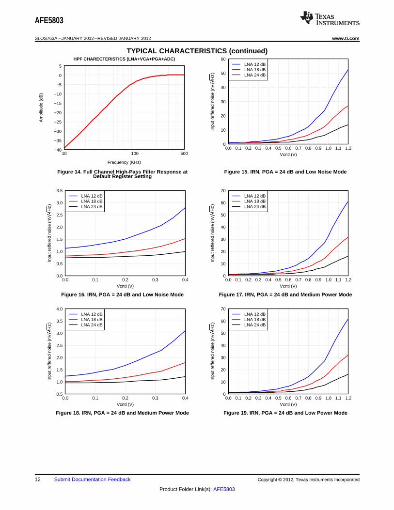
TYPICAL CHARACTERISTICS (continued)
Figure 14. Full Channel High-Pass Filter Response at Figure 15. IRN, PGA = 24 dB and Low Noise ModeDefault Register Setting
Figure 16. IRN, PGA = 24 dB and Low Noise Mode Figure 17. IRN, PGA = 24 dB and Medium Power Mode
Figure 18. IRN, PGA = 24 dB and Medium Power Mode Figure 19. IRN, PGA = 24 dB and Low Power Mode
12 Submit Documentation Feedback Copyright © 2012, Texas Instruments Incorporated
Product Folder Link(s): AFE5803
0.5
1.0
1.5
2.0
2.5
3.0
3.5
4.0
0.0 0.1 0.2 0.3 0.4Vcntl (V)
Inpu
t ref
fere
d no
ise
(nV
Hz
)
LNA 12 dBLNA 18 dBLNA 24 dB
30
50
70
90
110
130
150
170
190
210220
0.0 0.1 0.2 0.3 0.4 0.5 0.6 0.7 0.8 0.9 1.0 1.1 1.2Vcntl (V)
Out
put r
effe
red
nois
e (n
VH
z)
LNA 12 dBLNA 18 dBLNA 24 dB
40
60
80
100
120
140
160
180
200
220
240
260
280
300
0.0 0.1 0.2 0.3 0.4 0.5 0.6 0.7 0.8 0.9 1.0 1.1 1.2Vcntl (V)
Out
put r
effe
red
nois
e (n
VH
z)
LNA 12 dBLNA 18 dBLNA 24 dB
406080
100120140160180200220240260280300320340
0 0.1 0.2 0.3 0.4 0.5 0.6 0.7 0.8 0.9 1 1.1 1.2Vcntl (V)
Out
put r
effe
red
nois
e (n
VH
z)
LNA 12 dBLNA 18 dBLNA 24 dB
0.3
0.4
0.5
0.6
0.7
0.8
0.9
1.0
1.1
1.2
1.3
1.4
1.5
1.0 2.0 3.0 4.0 5.0 6.0 7.0 8.0 9.0 10.0 11.0 12.0Frequency (MHz)
Am
plitu
de (
nVH
z)
40.0
60.0
80.0
100.0
120.0
140.0
160.0
180.0
1.0 3.0 5.0 7.0 9.0 11.0 12.0Frequency (MHz)
Am
plitu
de (
nVH
z)
AFE5803
www.ti.com SLOS763A –JANUARY 2012–REVISED JANUARY 2012
TYPICAL CHARACTERISTICS (continued)
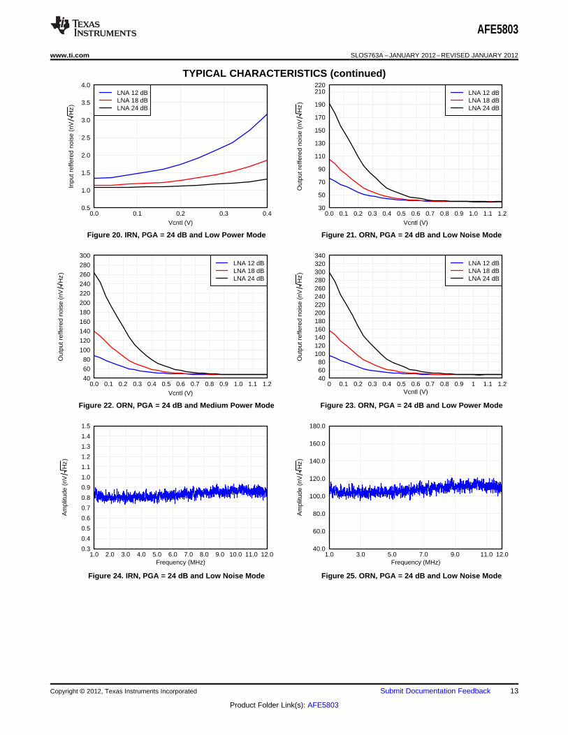
Figure 20. IRN, PGA = 24 dB and Low Power Mode Figure 21. ORN, PGA = 24 dB and Low Noise Mode
Figure 22. ORN, PGA = 24 dB and Medium Power Mode Figure 23. ORN, PGA = 24 dB and Low Power Mode
Figure 24. IRN, PGA = 24 dB and Low Noise Mode Figure 25. ORN, PGA = 24 dB and Low Noise Mode
Copyright © 2012, Texas Instruments Incorporated Submit Documentation Feedback 13
Product Folder Link(s): AFE5803

55
60
65
70
75
0.0 0.1 0.2 0.3 0.4 0.5 0.6 0.7 0.8 0.9 1.0 1.1 1.2Vcntl (V)
SN
R (
dBF
S)
24 dB PGA gain30 dB PGA gain
55
60
65
70
75
0.0 0.1 0.2 0.3 0.4 0.5 0.6 0.7 0.8 0.9 1.0 1.1 1.2Vcntl (V)
SN
R (
dBF
S)
24 dB PGA gain30 dB PGA gain
57
59
61
63
65
67
69
71
73
0 3 6 9 12 15 18 21 24 27 30 33 36 39 42Gain (dB)
SN
R (
dBF
S)
Low noiseLow power
0
1
2
3
4
5
6
7
8
9
50 100 150 200 250 300 350 400
Source Impedence (Ω)
Noi
se F
igur
e (d
B)
100 ohm act term200 ohm act term400 ohm act termWithout Termination
0
1
2
3
4
5
6
7
8
9
10
50 100 150 200 250 300 350 400
Source Impedence (Ω)
Noi
se F
igur
e (d
B)
50 ohm act term100 ohm act term200 ohm act term400 ohm act termWithout Termination
0
1
2
3
4
5
6
7
8
50 100 150 200 250 300 350 400
Source Impedence (Ω)
Noi
se F
igur
e (d
B)
50 ohm act term100 ohm act term200 ohm act term400 ohm act termNo Termination
AFE5803
SLOS763A –JANUARY 2012–REVISED JANUARY 2012 www.ti.com
TYPICAL CHARACTERISTICS (continued)
Figure 26. SNR, LNA = 18 dB and Low Noise Mode Figure 27. SNR, LNA = 18 dB and Low Power Mode
Figure 28. SNR vs. Different Power Modes Figure 29. Noise Figure, LNA = 12 dB and Low Noise Mode
Figure 30. Noise Figure, LNA = 18 dB and Low Noise Mode Figure 31. Noise Figure, LNA = 24 dB and Low Noise Mode
14 Submit Documentation Feedback Copyright © 2012, Texas Instruments Incorporated
Product Folder Link(s): AFE5803

1.5
2.5
3.5
4.5
50 100 150 200 250 300 350 400
Source Impedence (Ω)
Noi
se F
igur
e (d
B)
Low noiseLow powerMedium power
1
2
3
4
50 100 150 200 250 300 350 400
Source Impedence (Ω)
Noi
se F
igur
e (d
B)
Low noiseLow powerMedium power
−80.0
−75.0
−70.0
−65.0
−60.0
−55.0
−50.0
1 2 3 4 5 6 7 8 9 10Frequency (MHz)
HD
2 (d
B)
Low noiseLow powerMedium power
−75
−70
−65
−60
−55
−50
−45
1 2 3 4 5 6 7 8 9 10Frequency (MHz)
HD
3 (d
Bc)
Low noiseLow powerMedium power
−90
−85
−80
−75
−70
−65
−60
−55
−50
−45
−40
6 12 18 24 30 36Gain (dB)
HD
2 (d
Bc)
Low noiseLow powerMedium power
−90
−80
−70
−60
−50
−40
6 12 18 24 30 36Gain (dB)
HD
3 (d
Bc)
Low noiseLow powerMedium power
AFE5803
www.ti.com SLOS763A –JANUARY 2012–REVISED JANUARY 2012
TYPICAL CHARACTERISTICS (continued)
Figure 32. Noise Figure vs. Power Modes with 400 Ω Figure 33. Noise Figure vs. Power Modes withoutTermination Termination
Figure 34. HD2 vs. Frequency, Vin = 500 mVPP and Figure 35. HD3 vs. Frequency, Vin = 500 mVpp andVOUT = -1 dBFS VOUT = -1 dBFS
Figure 36. HD2 vs. Gain, LNA = 12 dB and Figure 37. HD3 vs. Gain, LNA = 12 dB and PGA = 24 dBand VOUT = -1 dBFSPGA = 24 dB and VOUT = -1 dBFS
Copyright © 2012, Texas Instruments Incorporated Submit Documentation Feedback 15
Product Folder Link(s): AFE5803
−90
−80
−70
−60
−50
−40
12 18 24 30 36 42Gain (dB)
HD
2 (d
Bc)
Low noiseLow powerMedium power
−90
−80
−70
−60
−50
−40
12 18 24 30 36 42Gain (dB)
HD
3 (d
Bc)
Low noiseLow powerMedium power
−90
−85
−80
−75
−70
−65
−60
−55
−50
−45
−40
18 24 30 36 42 48Gain (dB)
HD
2 (d
Bc)
Low noiseLow powerMedium power
−90
−80
−70
−60
−50
−40
18 21 24 27 30 33 36 39 42 45 48Gain (dB)
HD
3 (d
B)
Low noiseLow powerMedium power
−70
−66
−62
−58
−54
−50
14 18 22 26 30 34 38 42Gain (dB)
IMD
3 (d
BF
S)
Fin1=2MHz, Fin2=2.01MHzFin1=5MHz, Fin2=5.01MHz
G001
−70
−66
−62
−58
−54
−50
14 18 22 26 30 34 38 42Gain (dB)
IMD
3 (d
BF
S)
Fin1=2MHz, Fin2=2.01MHzFin1=5MHz, Fin2=5.01MHz
G001
AFE5803
SLOS763A –JANUARY 2012–REVISED JANUARY 2012 www.ti.com
TYPICAL CHARACTERISTICS (continued)
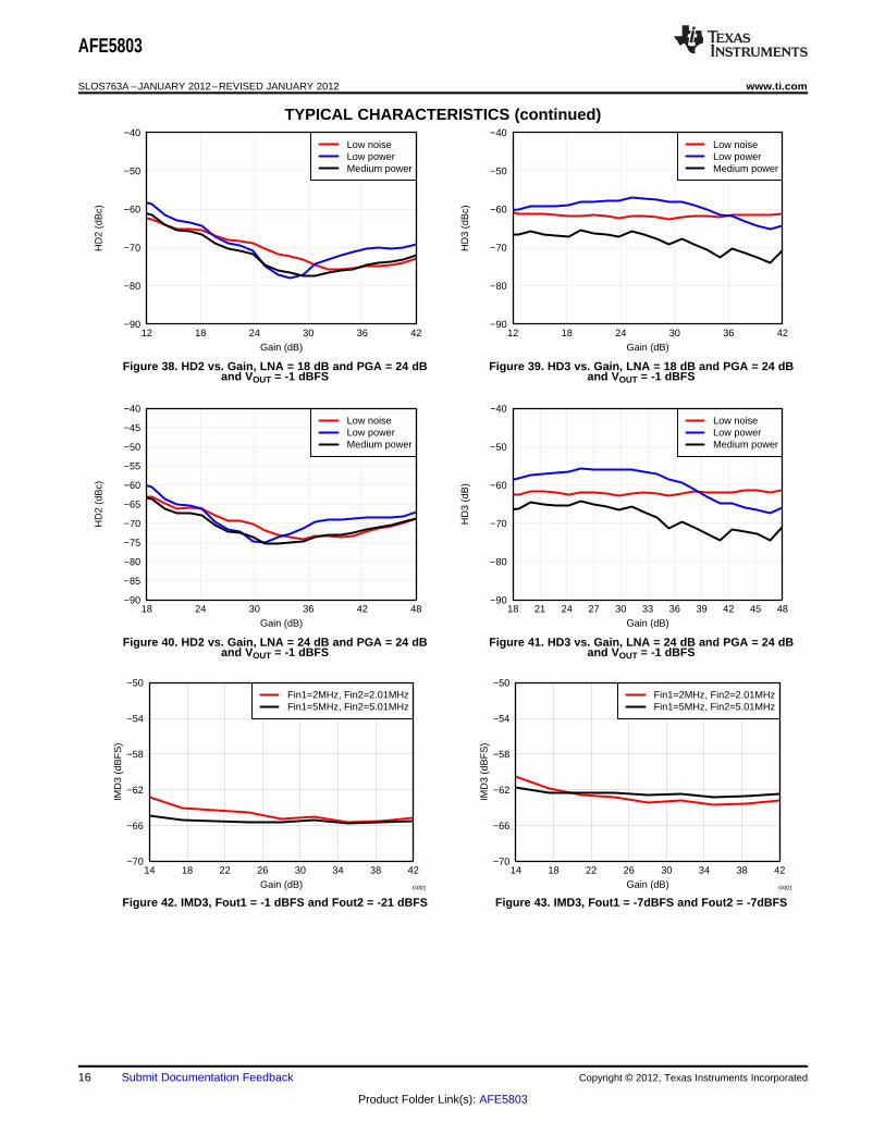
Figure 38. HD2 vs. Gain, LNA = 18 dB and PGA = 24 dB Figure 39. HD3 vs. Gain, LNA = 18 dB and PGA = 24 dBand VOUT = -1 dBFS and VOUT = -1 dBFS
Figure 40. HD2 vs. Gain, LNA = 24 dB and PGA = 24 dB Figure 41. HD3 vs. Gain, LNA = 24 dB and PGA = 24 dBand VOUT = -1 dBFS and VOUT = -1 dBFS
Figure 42. IMD3, Fout1 = -1 dBFS and Fout2 = -21 dBFS Figure 43. IMD3, Fout1 = -7dBFS and Fout2 = -7dBFS
16 Submit Documentation Feedback Copyright © 2012, Texas Instruments Incorporated
Product Folder Link(s): AFE5803

−75
−70
−65
−60
5 10 100 1000 2000
PSMR vs SUPPLY FREQUENCY
Supply frequency (kHz)
PS
MR
(dB
c)
Vcntl = 0Vcntl = 0.3Vcntl = 0.6Vcntl = 0.9
−80
−75
−70
−65
−60
−55
5 10 100 1000 2000
PSMR vs SUPPLY FREQUENCY
Supply frequency (kHz)
PS
MR
(dB
c)
Vcntl = 0Vcntl = 0.3Vcntl = 0.6Vcntl = 0.9
−90
−80
−70
−60
−50
−40
−30
−20
5 10 100 1000 2000
3V PSRR vs SUPPLY FREQUENCY
Supply frequency (kHz)
PS
RR
wrt
sup
ply
tone
(dB
)
Vcntl = 0Vcntl = 0.3Vcntl = 0.6Vcntl = 0.9
−90
−80
−70
−60
−50
−40
−30
−20
5 10 100 1000 2000
5V PSRR vs SUPPLY FREQUENCY
Supply frequency (kHz)
PS
RR
wrt
sup
ply
tone
(dB
)Vcntl = 0Vcntl = 0.3Vcntl = 0.6Vcntl = 0.9
0.0 0.5 1.0 1.5 2.0 2.5 3.00.0
2000.0
4000.0
6000.0
8000.0
10000.0
12000.0
14000.0
16000.0
18000.0
20000.0
−0.10.00.10.20.30.40.50.60.70.80.91.01.11.21.3
Time (µs)
Out
put C
ode
Vcn
tl (V
)
Output CodeVcntl
0.0 0.2 0.5 0.8 1.0 1.2 1.5 1.8 2.0 2.2 2.50.0
2000.0
4000.0
6000.0
8000.0
10000.0
12000.0
14000.0
16000.0
18000.0
20000.0
−0.10.00.10.20.30.40.50.60.70.80.91.01.11.21.3
Time (µs)
Out
put C
ode
Vcn
tl (V
)
Output CodeVcntl
AFE5803
www.ti.com SLOS763A –JANUARY 2012–REVISED JANUARY 2012
TYPICAL CHARACTERISTICS (continued)
Figure 44. AVDD Power Supply Modulation Ratio, Figure 45. AVDD_5V Power Supply Modulation Ratio,100mVPP Supply Noise with Different Frequencies100 mVPP Supply Noise with Different Frequencies
Figure 46. AVDD Power Supply Rejection Ratio, 100mVPP Figure 47. AVDD_5 V Power Supply Rejection Ratio,Supply Noise with Different Frequencies 100mVPP Supply Noise with Different Frequencies
Figure 48. VCNTL Response Time, LNA = 18 dB Figure 49. VCNTL Response Time, LNA = 18 dBand PGA = 24 dB and PGA = 24 dB
Copyright © 2012, Texas Instruments Incorporated Submit Documentation Feedback 17
Product Folder Link(s): AFE5803

−1.2
−1.0
−0.8
−0.6
−0.4
−0.2
0.0
0.2
0.4
0.6
0.8
1.0
1.2
0.0 2.0 4.0 6.0 8.0 10.0 12.0 14.0 16.0 18.0 20.0Time (µs)
Inpu
t (V
)
−1.2
−1.0
−0.8
−0.6
−0.4
−0.2
0.0
0.2
0.4
0.6
0.8
1.0
1.2
0.0 2.0 4.0 6.0 8.0 10.0 12.0 14.0 16.0 18.0 20.0Time (µs)
Inpu
t (V
)
−10000.0
−8000.0
−6000.0
−4000.0
−2000.0
0.0
2000.0
4000.0
6000.0
8000.0
10000.0
0.0 1.0 2.0 3.0 4.0 5.0 6.0Time (µs)
Out
put C
ode
Positive overloadNegative overloadAverage
−10000
−8000
−6000
−4000
−2000
0
2000
4000
6000
8000
10000
0 0.5 1 1.5 2 2.5 3 3.5 4 4.5 5Time (µs)
Out
put C
ode
47nF15nF
−40
−35
−30
−25
−20
−15
−10
−5
0
5
10
0 0.2 0.4 0.6 0.8 1 1.2 1.4 1.6 1.8 2Frequency (MHz)
Gai
n (d
B) k=2
k=3k=4k=5k=6k=7k=8k=9k=10
G000
−2000
−1600
−1200
−800
−400
0
400
800
1200
1600
2000
1 1.5 2 2.5 3 3.5 4 4.5 5Time (µs)
Out
put C
ode
47nF15nF
AFE5803
SLOS763A –JANUARY 2012–REVISED JANUARY 2012 www.ti.com
TYPICAL CHARACTERISTICS (continued)
Figure 50. Pulse Inversion Asymmetrical Positive Input Figure 51. Pulse Inversion Asymmetrical Negative Input
Figure 52. Pulse Inversion, VIN = 2 VPP, PRF = 1 KHz, Gain Figure 53. Overload Recovery Response vs. INM= 21 dB Capacitor, VIN = 50 mVPP/100 µVPP, Max Gain
Figure 54. Overload Recovery Response vs. INM Capacitor Figure 55. Digital High-Pass Filter Response(Zoomed), VIN = 50 mVPP/100 µVPP, Max Gain
18 Submit Documentation Feedback Copyright © 2012, Texas Instruments Incorporated
Product Folder Link(s): AFE5803

AFE5803
www.ti.com SLOS763A –JANUARY 2012–REVISED JANUARY 2012
TIMING CHARACTERISTICS (1)
Typical values are at 25°C, AVDD_5V = 5 V, AVDD = 3.3 V, AVDD_ADC = 1.8 V, DVDD = 1.8 V, Differential clock, CLOAD =5pF, RLOAD = 100 Ω, 14Bit, sample rate = 65MSPS, unless otherwise noted. Minimum and maximum values are across thefull temperature range TMIN = 0°C to TMAX = 85°C with AVDD_5V = 5 V, AVDD = 3.3 V, AVDD_ADC = 1.8 V, DVDD = 1.8 V
PARAMETER TEST CONDITIONS MIN TYP MAX UNIT
The delay in time between the rising edge of the input samplingta Aperture delay 0.7 3 nsclock and the actual time at which the sampling occurs
Aperture delay Across channels within the same device ±150 psmatching
tj Aperture jitter 450 Fs rms
InputADC latency Default, after reset, or / 0 x 2 [12] = 1, LOW_LATENCY = 1 11/8 clock
cycles
Data and frame clock Input clock rising edge (zero cross) to frame clock rising edge (zerotdelay 3 5.4 7 nsdelay cross) minus 3/7 of the input clock period (T).
Δtdelay Delay variation At fixed supply and 20°C T difference. Device to device –1 1 ns
tRISE Rise time measured from –100 mV to 100 mV Fall time measured 0.14 nsData rise time Data fallfrom 100 mV to –100 mV 10 MHz < fCLKIN < 65 MHztimetFALL 0.15
tFCLKRISE Frame clock rise time Rise time measured from –100mV to 100mV Fall time measured 0.14 nsFrame clock fall time from 100 mV to –100 mV 10 MHz < fCLKIN < 65MHztFCLKFALL 0.15
Frame clock duty cycle Zero crossing of the rising edge to zero crossing of the falling edge 48% 50% 52%
tDCLKRISE Rise time measured from –100mV to 100mV Fall time measured 0.13 nsBit clock rise time Bitfrom 100 mV to –100 mV 10 MHz < fCLKIN < 65MHzclock fall timetDCLKFALL 0.12
Zero crossing of the rising edge to zero crossing of the falling edgeBit clock duty cycle 46% 54%10 MHz < fCLKIN < 65 MHz
(1) Timing parameters are ensured by design and characterization; not production tested.
OUTPUT INTERFACE TIMING (1) (2) (3)
Setup Time (tsu), ns Hold Time (th), ns tPROG = (3/7)x T + tdelay, ns(for output data and frame clock) (for output data and frame clock)fCLKIN,Input Clock Input Clock Zero-Cross (rising edge)Data Valid to Input Clock Input Clock Zero-Crossing to DataFrequency to Frame Clock Zero-Cross (risingZero-Crossing Invalid edge)
MHz MIN TYP MAX MIN TYP MAX MIN TYP MAX
65/14bit 0.24 0.37 0.24 0.38 11 12 12.5
50/14bit 0.41 0.54 0.46 0.57 13 13.9 14.4
40/14bit 0.55 0.70 0.61 0.73 15 16 16.7
30/14bit 0.87 1.10 0.94 1.1 18.5 19.5 20.1
20/14bit 1.30 1.56 1.46 1.6 25.7 26.7 27.3
(1) FCLK timing is the same as for the output data lines. It has the same relation to DCLK as the data pins. Setup and hold are the samefor the data and the frame clock.
(2) Data valid is logic HIGH = +100mV and logic LOW = -100mV(3) Timing parameters are ensured by design and characterization; not production tested.
Copyright © 2012, Texas Instruments Incorporated Submit Documentation Feedback 19
Product Folder Link(s): AFE5803
T0434-0
1
Bit C
lock
DC
LK
P
Outp
ut D
ata
Pair
t su
CH
iout
t h
t ht s
u
DC
LK
M
Dn +
1D
n
12-Bit 6x serialization mode 14-Bit 7x serialization mode
LVDS Setup and Hold Timing
t PR
OG
Fram
e C
lock
FCLK
Freq
=f C
LKIN
Inpu
t Clo
ck
CLK
INFr
eq=
f CLK
IN
SA
MP
LE N
-1
D13
(D0)
Dat
a bi
t in
MS
B F
irst
mod
e
Dat
a bi
t in
LSB
Fir
st m
ode
Bit
Clo
ck
DC
LKFr
eq=
7x
f CLK
IN
Out
put D
ata
CH
nOU
T
Dat
a ra
te=
14x
f CLK
IN
D11
(D0)
D10
(D1)
SA
MP
LE N
t PR
OG
T
Inpu
t Sig
nal
t a
Sam
ple
NS
ampl
eN
+Cd
Cd
cloc
k cy
cles
late
ncy
D0
(D13
)
D13
(D0)
D12
(D1)
D11
(D2)
D10
(D3)
D9
(D4)
D8
(D5)
D7
(D6)
D6
(D7)
D5
(D8)
D4
(D9)
D3
(D10
)
D2
(D11
)
SA
MP
LE N
-Cd
D1
(D12
)
Sam
ple
N+C
d+1
D1
(D12
)D
0(D
13)
D13
(D0)
D12
(D1)
D11
(D2)
D10
(D3)
D9
(D4)
D8
(D5)
D7
(D6)
D6
(D7)
D5
(D8)
D4
(D9)
D3
(D10
)
D2
(D11
)D
1(D
12)
D0
(D13
)
D13
(D0)
D12
(D1)
D11
(D2)
D10
(D3)
D9
(D4)
D8
(D5)
D7
(D6)
D6
(D7)
D5
(D8)
D4
(D9)
D3
(D10
)
D2
(D11
)
D1
(D12
)
D0
(D13
)
t a
AFE5803
SLOS763A –JANUARY 2012–REVISED JANUARY 2012 www.ti.com
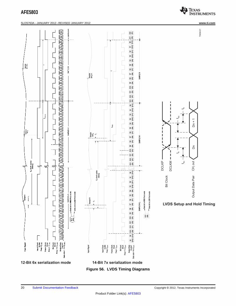
Figure 56. LVDS Timing Diagrams
20 Submit Documentation Feedback Copyright © 2012, Texas Instruments Incorporated
Product Folder Link(s): AFE5803

D15 D14 D13 D12 D11 D10 D9 D8 D7 D6 D5 D4 D3 D2 D1 D0A7 A6 A5 A4 A3 A2 A1 A0
SEN
SCLK
SDATA
RESET
Data Latched On Rising Edge of SCLK
Start Sequence
Start Sequence
End Sequence
End Sequence
t7
t6
t2
t4
t1
t5
t3
T0384-01
AFE5803
www.ti.com SLOS763A –JANUARY 2012–REVISED JANUARY 2012
LVDS Output Interface Description
AFE5803 has LVDS output interface which supports multiple output formats. The ADC resolutions can beconfigured as 12bit or 14bit as shown in the LVDS timing diagrams Figure 56. The ADCs in the AFE5803 arerunning at 14bit; 2 LSBs are removed when 12-bit output is selected; and two 0s are added at LSBs when 16-bitoutput is selected. Appropriate ADC resolutions can be selected for optimizing system performance-costeffectiveness. When the devices run at 16bit mode, higher end FPGAs are required to process higher rate ofLVDS data. Corresponding register settings are listed in Table 1.
Table 1. Corresponding Register Settings
LVDS Rate 12 bit (6X DCLK) 14 bit (7X DCLK) 16 bit (8X DCLK)
Reg 3 [14:13] 11 00 01
Reg 4 [2:0] 010 000 000
Description 2 LSBs removed N/A 2 0s added at LSBs
SERIAL REGISTER TIMING
Serial Register Write Description
Programming of different modes can be done through the serial interface formed by pins SEN (serial interfaceenable), SCLK (serial interface clock), SDATA (serial interface data) and RESET. All these pins have a pull-downresistor to GND of 100kΩ. Serial shift of bits into the device is enabled when SEN is low. Serial data SDATA islatched at every rising edge of SCLK when SEN is active (low). The serial data is loaded into the register atevery 24th SCLK rising edge when SEN is low. If the word length exceeds a multiple of 24 bits, the excess bitsare ignored. Data can be loaded in multiple of 24-bit words within a single active SEN pulse (there is an internalcounter that counts groups of 24 clocks after the falling edge of SEN). The interface can work with the SCLKfrequency from 20 MHz down to low speeds (few Hertz) and even with non-50% duty cycle SCLK. The data isdivided into two main portions: a register address (8 bits) and the data itself (16 bits), to load on the addressedregister. When writing to a register with unused bits, these should be set to 0. Figure 57 illustrates this process.
Figure 57. SPI Timing
Copyright © 2012, Texas Instruments Incorporated Submit Documentation Feedback 21
Product Folder Link(s): AFE5803

x x x x x x x x x x x x x x x xA7 A6 A5 A4 A3 A2 A1 A0
SEN
SCLK
SDATA
SDOUT
Start Sequence End Sequence
t7
t6
t2
t4
t1
t5
t3
D15 D14 D13 D12 D11 D10 D9 D8 D7 D6 D5 D4 D3 D2 D1 D0
t8
AFE5803
SLOS763A –JANUARY 2012–REVISED JANUARY 2012 www.ti.com
SPI Timing Characteristics
Minimum values across full temperature range TMIN = 0°C to TMAX = 85°C, AVDD_5V =5.0V, AVDD=3.3V,AVDD_ADC=1.8V, DVDD=1.8V
PARAMETER DESCRIPTION MIN TYP MAX UNIT
t1 SCLK period 50 ns
t2 SCLK high time 20 ns
t3 SCLK low time 20 ns
t4 Data setup time 5 ns
t5 Data hold time 5 ns
t6 SEN fall to SCLK rise 8 ns
t7 Time between last SCLK rising edge to SEN rising edge 8 ns
t8 SDOUT delay 12 20 28 ns
Register Readout
The device includes an option where the contents of the internal registers can be read back. This may be usefulas a diagnostic test to verify the serial interface communication between the external controller and the AFE.First, the <REGISTER READOUT ENABLE> bit (Reg0[1]) needs to be set to '1'. Then user should initiate aserial interface cycle specifying the address of the register (A7-A0) whose content has to be read. The data bitsare "don’t care". The device will output the contents (D15-D0) of the selected register on the SDOUT pin.SDOUT has a typical delay t8 of 20nS from the falling edge of the SCLK. For lower speed SCLK, SDOUT can belatched on the rising edge of SCLK. For higher speed SCLK,e.g. the SCLK period lesser than 60nS, it would bebetter to latch the SDOUT at the next falling edge of SCLK. The following timing diagram shows this operation(the time specifications follow the same information provided. In the readout mode, users still can access the<REGISTER READOUT ENABLE> through SDATA/SCLK/SEN. To enable serial register writes, set the<REGISTER READOUT ENABLE> bit back to '0'.
Figure 58. Serial Interface Register Read
The AFE5803 SDOUT buffer is tri-stated and will get enabled only when 0[1] (REGISTER READOUT ENABLE)is enabled. SDOUT pins from multiple AFE5803s can be tied together without any pull-up resistors. Level shifterSN74AUP1T04 can be used to convert 1.8V logic to 2.5V/3.3V logics if needed.
22 Submit Documentation Feedback Copyright © 2012, Texas Instruments Incorporated
Product Folder Link(s): AFE5803
t1
t2
t3
Device Ready forSerial Register Write
Device Ready for
Data ConversionStart of Clock
AVDDAVDD_5V
AVDD_ADC
DVDD
RESET
SEN
CLKP_ADC
t4 t7
t8
t6
t5
AFE5803
www.ti.com SLOS763A –JANUARY 2012–REVISED JANUARY 2012
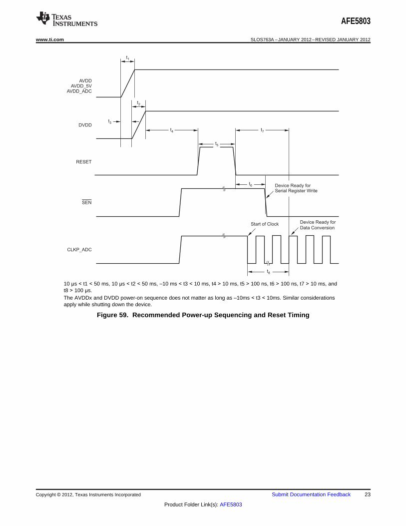
10 µs < t1 < 50 ms, 10 µs < t2 < 50 ms, –10 ms < t3 < 10 ms, t4 > 10 ms, t5 > 100 ns, t6 > 100 ns, t7 > 10 ms, andt8 > 100 µs.The AVDDx and DVDD power-on sequence does not matter as long as –10ms < t3 < 10ms. Similar considerationsapply while shutting down the device.
Figure 59. Recommended Power-up Sequencing and Reset Timing
Copyright © 2012, Texas Instruments Incorporated Submit Documentation Feedback 23
Product Folder Link(s): AFE5803

AFE5803
SLOS763A –JANUARY 2012–REVISED JANUARY 2012 www.ti.com
REGISTER MAP
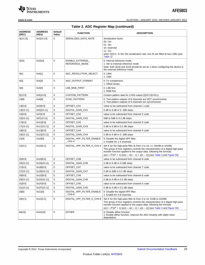
ADC Register Map
A reset process is required at the AFE5803 initialization stage. Initialization can be done in one of two ways:1. Through a hardware reset, by applying a positive pulse at the RESET pin2. Through a software reset, using the serial interface, by setting the SOFTWARE RESET bit to high. Setting
this bit initializes the internal registers to the respective default values (all zeros) and then self-resets theSOFTWARE RESET bit to low. In this case, the RESET pin can stay low (inactive).
After reset, all ADC and VCA registers are set to ‘0’, i.e. default settings. During register programming, allreserved/unlisted register bits need to be set as ‘0’. Register settings are maintained when the AFE5803 is ineither partial power down mode or complete power down mode.
Table 2. ADC Register Map
ADDRESS ADDRESS Default FUNCTION DESCRIPTION(DEC) (HEX) Value
0[0] 0x0[0] 0 SOFTWARE_RESET 0: Normal operation;1: Resets the device and self-clears the bit to '0'
0[1] 0x0[1] 0 REGISTER_READOUT_ENABLE 0:Disables readout;1: enables readout of register at SDOUT Pin
1[0] 0x1[0] 0 ADC_COMPLETE_PDN 0: Normal1: Complete Power down
1[1] 0x1[1] 0 LVDS_OUTPUT_DISABLE 0: Output Enabled;1: Output disabled
1[9:2] 0x1[9:2] 0 ADC_PDN_CH<7:0> 0: Normal operation;1: Power down. Power down Individual ADC channels.1[9]→CH8…1[2]→CH1
1[10] 0x1[10] 0 PARTIAL_PDN 0: Normal Operation;1: Partial Power Down ADC
1[11] 0x1[11] 0 LOW_FREQUENCY_ 0: No suppression;NOISE_SUPPRESSION 1: Suppression Enabled
1[13] 0x1[13] 0 EXT_REF 0: Internal Reference;1: External Reference. VREF_IN is used. Both 3[15] and 1[13] should be setas 1 in the external reference mode
1[14] 0x1[14] 0 LVDS_OUTPUT_RATE_2X 0: 1x rate;1: 2x rate. Combines data from 2 channels on 1 LVDS pair. When ADC clockrate is low, this feature can be used
1[15] 0x1[15] 0 SINGLE-ENDED_CLK_MODE 0: Differential clock input;1: Single-ended clock input
2[2:0] 0x2[2:0] 0 RESERVED Set to 0
2[10:3] 0x2[10:3] 0 POWER-DOWN_LVDS 0: Normal operation;1: PDN Individual LVDS outputs. 2[10]→CH8…2[3]→CH1
2[11] 0x2[11] 0 AVERAGING_ENABLE 0: No averaging;1: Average 2 channels to increase SNR
2[12] 0x2[12] 0 LOW_LATENCY 0: Default Latency with digital features supported, 11 cycle latency1: Low Latency with digital features bypassed, 8 cycle latency
2[15:13] 0x2[15:3] 0 TEST_PATTERN_MODES 000: Normal operation;001: Sync;010: De-skew;011: Custom;100:All 1's;101: Toggle;110: All 0's;111: Ramp
3[7:0] 0x3[7:0] 0 INVERT_CHANNELS 0: No inverting;1:Invert channel digital output. 3[7]→CH8;3[0]→CH1
3[8] 0x3[8] 0 CHANNEL_OFFSET_ 0: No offset subtraction;SUBSTRACTION_ENABLE 1: Offset value Subtract Enabled
3[9:11] 0x3[9:11] 0 RESERVED Set to 0
3[12] 0x3[12] 0 DIGITAL_GAIN_ENABLE 0: No digital gain;1: Digital gain Enabled
24 Submit Documentation Feedback Copyright © 2012, Texas Instruments Incorporated
Product Folder Link(s): AFE5803
AFE5803
www.ti.com SLOS763A –JANUARY 2012–REVISED JANUARY 2012
Table 2. ADC Register Map (continued)ADDRESS ADDRESS Default FUNCTION DESCRIPTION(DEC) (HEX) Value
3[14:13] 0x3[14:13] 0 SERIALIZED_DATA_RATE Serialization factor00: 14x01: 16x10: reserved11: 12xwhen 4[1]=1. In the 16x serialization rate, two 0s are filled at two LSBs (seeTable 1)
3[15] 0x3[15] 0 ENABLE_EXTERNAL_ 0: Internal reference mode;REFERENCE_MODE 1: Set to external reference mode
Note: both 3[15] and 1[13] should be set as 1 when configuring the device inthe external reference mode
4[1] 0x4[1] 0 ADC_RESOLUTION_SELECT 0: 14bit;1: 12bit
4[3] 0x4[3] 0 ADC_OUTPUT_FORMAT 0: 2's complement;1: Offset binary
4[4] 0x4[4] 0 LSB_MSB_FIRST 0: LSB first;1: MSB first
5[13:0] 0x5[13:0] 0 CUSTOM_PATTERN Custom pattern data for LVDS output (2[15:13]=011)
10[8] 0xA[8] 0 SYNC_PATTERN 0: Test pattern outputs of 8 channels are NOT synchronized.1: Test pattern outputs of 8 channels are synchronized.
13[9:0] 0xD[9:0] 0 OFFSET_CH1 Value to be subtracted from channel 1 code
13[15:11] 0xD[15:11] 0 DIGITAL_GAIN_CH1 0 dB to 6 dB in 0. 2dB steps
15[9:0] 0xF[9:0] 0 OFFSET_CH2 value to be subtracted from channel 2 code
15[15:11] 0xF[15:11] 0 DIGITAL_GAIN_CH2 0dB to 6dB in 0.2 dB steps
17[9:0] 0x11[9:0] 0 OFFSET_CH3 value to be subtracted from channel 3 code
17[15:11] 0x11[15:11] 0 DIGITAL_GAIN_CH3 0 dB to 6 dB in 0.2 dB steps
19[9:0] 0x13[9:0] 0 OFFSET_CH4 value to be subtracted from channel 4 code
19[15:11] 0x13[15:11] 0 DIGITAL_GAIN_CH4 0 dB to 6 dB in 0. 2dB steps
21[0] 0x15[0] 0 DIGITAL_HPF_FILTER_ENABLE 0: Disable the digital HPF filter;_ CH1-4 1: Enable for 1-4 channels
21[4:1] 0x15[4:1] 0 DIGITAL_HPF_FILTER_K_CH1-4 Set K for the high-pass filter (k from 2 to 10, i.e. 0010B to 1010B).This group of four registers controls the characteristics of a digital high-passtransfer function applied to the output data, following the formula:
y(n) = 2k/(2k + 1) [x(n) – x(n – 1) + y(n – 1)] (see Table 3 and Figure 55)
25[9:0] 0x19[9:0] 0 OFFSET_CH8 value to be subtracted from channel 8 code
25[15:11] 0x19[15:11] 0 DIGITAL_GAIN_CH8 0 dB to 6 dB in 0.2dB steps
27[9:0] 0x1B[9:0] 0 OFFSET_CH7 value to be subtracted from channel 7 code
27[15:11] 0x1B[15:11] 0 DIGITAL_GAIN_CH7 0 dB to 6dB in 0.2 dB steps
29[9:0] 0x1D[9:0] 0 OFFSET_CH6 value to be subtracted from channel 6 code
29[15:11] 0x1D[15:11] 0 DIGITAL_GAIN_CH6 0 dB to 6 dB in 0.2 dB steps
31[9:0] 0x1F[9:0] 0 OFFSET_CH5 value to be subtracted from channel 5 code
31[15:11] 0x1F[15:11] 0 DIGITAL_GAIN_CH5 0 dB to 6 dB in 0.2 dB steps
33[0] 0x21[0] 0 DIGITAL_HPF_FILTER_ENABLE 0: Disable the digital HPF filter;_ CH5-8 1: Enable for 5-8 channels
33[4:1] 0x21[4:1] 0 DIGITAL_HPF_FILTER_K_CH5-8 Set K for the high-pass filter (k from 2 to 10, 010B to 1010B)This group of four registers controls the characteristics of a digital high-passtransfer function applied to the output data, following the formula:
y(n) = 2k/(2k + 1) [x(n) – x(n – 1) + y(n – 1)] (see Table 3 and Figure 55)
66[15] 0x42[15] 0 DITHER 0: Disable dither function.1: Enable dither function. Improve the ADC linearity with slight noisedegradation.
Copyright © 2012, Texas Instruments Incorporated Submit Documentation Feedback 25
Product Folder Link(s): AFE5803

Digital OffsetDefault=No
ADCOutput 12/14b
FinalDigitalOutput12/14b
DigitalGain
Default=0
ChannelAverage
Default=No
Digital HPFDefault = No
( ) ( ) ( ) ( )2
k
k
2y n = x n x n 1 y n 1
1é ù- - + -ë û+
AFE5803
SLOS763A –JANUARY 2012–REVISED JANUARY 2012 www.ti.com
ADC Register/Digital Processing Description
The ADC in the AFE5803 has extensive digital processing functionalities which can be used to enhanceultrasound system performance. The digital processing blocks are arranged as in Figure 60.
Figure 60. ADC Digital Block Diagram
AVERAGING_ENABLE: Address: 2[11]
When set to 1, two samples, corresponding to two consecutive channels, are averaged (channel 1 with 2, 3 with4, 5 with 6, and 7 with 8). If both channels receive the same input, the net effect is an improvement in SNR. Theaveraging is performed as:• Channel 1 + channel 2 comes out on channel 3• Channel 3 + channel 4 comes out on channel 4• Channel 5 + channel 6 comes out on channel 5• Channel 7 + channel 8 comes out on channel 6
ADC_OUTPUT_FORMAT: Address: 4[3]
The ADC output, by default, is in 2’s-complement mode. Programming the ADC_OUTPUT_FORMAT bit to 1inverts the MSB, and the output becomes straight-offset binary mode.
DIGITAL_GAIN_ENABLE: Address: 3[12]
Setting this bit to 1 applies to each channel i the corresponding gain given by DIGTAL_GAIN_CHi <15:11>. Thegain is given as 0dB + 0.2dB × DIGTAL_GAIN_CHi<15:11>. For instance, if DIGTAL_GAIN_CH5<15:11> = 3,channel 5 is increased by 0.6dB gain. DIGTAL_GAIN_CHi <15:11> = 31 produces the same effect asDIGTAL_GAIN_CHi <15:11> = 30, setting the gain of channel i to 6dB.
DIGITAL_HPF_ENABLE• CH1-4: Address 21[0]• CH5-8: Address 33[0]
DIGITAL_HPF_FILTER_K_CHX• CH1-4: Address 21[4:1]• CH5-8: Address 3[4:1]
This group of registers controls the characteristics of a digital high-pass transfer function applied to the outputdata, following Equation 1.
(1)
These digital HPF registers (one for the first four channels and one for the second group of four channels)describe the setting of K. The digital high pass filter can be used to suppress low frequency noise whichcommonly exists in ultrasound echo signals. The digital filter can significantly benefit near field recovery time dueto T/R switch low frequency response. Table 3 shows the cut-off frequency vs K, also see Figure 55.
26 Submit Documentation Feedback Copyright © 2012, Texas Instruments Incorporated
Product Folder Link(s): AFE5803

AFE5803
www.ti.com SLOS763A –JANUARY 2012–REVISED JANUARY 2012
Table 3. Digital HPF –1dB Corner Frequency vs K and Fs
k 40 MSPS 50 MSPS 65 MSPS
2 2780 KHz 3480 KHz 4520 KHz
3 1490 KHz 1860 KHz 2420 KHz
4 770 KHz 960 KHz 1250 KHz
LOW_FREQUENCY_NOISE_SUPPRESSION: Address: 1[11]
The low-frequency noise suppression mode is especially useful in applications where good noise performance isdesired in the frequency band of 0MHz to 1MHz (around dc). Setting this mode shifts the low-frequency noise ofthe AFE5803 to approximately Fs/2, thereby moving the noise floor around dc to a much lower value. Register bit1[11] is used for enabling or disabling this feature. When this feature is enabled, power consumption of thedevice will be increased by approximate 1 mW/CH.
LVDS_OUTPUT_RATE_2X: Address: 1[14]
The output data always uses a DDR format, with valid/different bits on the positive as well as the negative edgesof the LVDS bit clock, DCLK. The output rate is set by default to 1X (LVDS_OUTPUT_RATE_2X = 0), whereeach ADC has one LVDS stream associated with it. If the sampling rate is low enough, two ADCs can share oneLVDS stream, in this way lowering the power consumption devoted to the interface. The unused outputs willoutput zero. To avoid consumption from those outputs, no termination should be connected to them. Thedistribution on the used output pairs is done in the following way:• Channel 1 and channel 2 come out on channel 3. Channel 1 comes out first.• Channel 3 and channel 4 come out on channel 4. Channel 3 comes out first.• Channel 5 and channel 6 come out on channel 5. Channel 5 comes out first.• Channel 7 and channel 8 come out on channel 6. Channel 7 comes out first
CHANNEL_OFFSET_SUBSTRACTION_ENABLE: Address: 3[8]
Setting this bit to 1 enables the subtraction of the value on the corresponding OFFSET_CHx<9:0> (offset forchannel i) from the ADC output. The number is specified in 2s-complement format. For example,OFFSET_CHx<9:0> = 11 1000 0000 means subtract –128. For OFFSET_CHx<9:0> = 00 0111 1111 the effect isto subtract 127. In effect, both addition and subtraction can be performed. Note that the offset is applied beforethe digital gain (see DIGITAL_GAIN_ENABLE). The whole data path is 2s-complement throughout internally, withdigital gain being the last step. Only when ADC_OUTPUT_FORMAT=1 (straight binary output format) is the2s-complement word translated into offset binary at the end.
SERIALIZED_DATA_RATE: Address: 3[14:13]
See Table 1 for detail description.
TEST_PATTERN_MODES: Address: 2[15:13]
The AFE5803 can output a variety of test patterns on the LVDS outputs. These test patterns replace the normalADC data output. The device may also be made to output 6 preset patterns:1. Ramp: Setting Register 2[15:13]=111causes all the channels to output a repeating full-scale ramp pattern.
The ramp increments from zero code to full-scale code in steps of 1LSB every clock cycle. After hitting thefull-scale code, it returns back to zero code and ramps again.
2. Zeros: The device can be programmed to output all zeros by setting Register 2[15:13]=110;3. Ones: The device can be programmed to output all 1s by setting Register 2[15:13]=100;4. Deskew Patten: When 2[15:13]=010; this mode replaces the 14-bit ADC output with the 01010101010101
word.5. Sync Pattern: When 2[15:13]=001, the normal ADC output is replaced by a fixed 11111110000000 word.6. Toggle: When 2[15:13]=101, the normal ADC output is alternating between 1's and 0's. The start state of
ADC word can be either 1's or 0's.7. Custom Pattern: It can be enabled when 2[15:13]= 011;. Users can write the required VALUE into register
bits <CUSTOM PATTERN> which is Register 5[13:0]. Then the device will output VALUE at its outputs,about 3 to 4 ADC clock cycles after the 24th rising edge of SCLK. So, the time taken to write one value is 24
Copyright © 2012, Texas Instruments Incorporated Submit Documentation Feedback 27
Product Folder Link(s): AFE5803

AFE5803
SLOS763A –JANUARY 2012–REVISED JANUARY 2012 www.ti.com
SCLK clock cycles + 4 ADC clock cycles. To change the customer pattern value, users can repeat writingRegister 5[13:0] with a new value. Due to the speed limit of SPI, the refresh rate of the custom pattern maynot be high. For example, 128 points custom pattern will take approximately 128 x (24 SCLK clock cycles + 4ADC clock cycles).
NOTEonly one of the above patterns can be active at any given instant.
SYNC_PATTERN: Address: 10[8]
By enabling this bit, all channels' test pattern outputs are synchronized. When 10[8] is set as 1, the ramppatterns of all 8 channels start simultaneously.
28 Submit Documentation Feedback Copyright © 2012, Texas Instruments Incorporated
Product Folder Link(s): AFE5803

AFE5803
www.ti.com SLOS763A –JANUARY 2012–REVISED JANUARY 2012
VCA Register Map
Table 4. VCA Register Map
ADDRESS ADDRESS Default FUNCTION DESCRIPTION(DEC) (HEX) Value
51[0] 0x33[0] 0 RESERVED 0
51[3:1] 0x33[3:1] 0 LPF_PROGRAMMABILITY 000: 15MHz,010: 20MHz,011: 30MHz,100: 10MHz
51[4] 0x33[4] 0 PGA_INTEGRATOR_DISABLE 0: Enable(PGA_HPF_DISABLE) 1: Disables offset integrator for PGA. See explanation for the PGA
integrator function in APPLICATION INFORMATION section
51[6:5] 0x33[6:5] 0 PGA_CURRENT_CLAMP_LEVEL 00: –2dBFS;10: 0dBFS;01:–4dBFS when 51[7]=0Note: the current clamp circuit makes sure that PGA output is in linearrange. For example, at 00 setting, PGA output HD3 will be worsen by3dB at –2dBFS ADC input. In normal operation, the current clampfunction can be set as 00
51[7] 0x33[7] 0 PGA_CURRENT_CLAMP_DISABLE 0:Enables the PGA current clamp circuit;1:Disables the PGA current clamp circuit before the PGA outputs.51[6:5] determines the current clamp level
51[13] 0x33[13] 0 PGA_GAIN_CONTROL 0:24dB;1:30dB.
52[4:0] 0x34[4:0] 0 ACTIVE_TERMINATION_ See Table 6 Reg 52[5] should be set as '1' to access these bitsINDIVIDUAL_RESISTOR_CNTL
52[5] 0x34[5] 0 ACTIVE_TERMINATION_ 0: Disables;INDIVIDUAL_RESISTOR_ENABLE 1: Enables internal active termination individual resistor control
52[7:6] 0x34[7:6] 0 PRESET_ACTIVE_ TERMINATIONS 00: 50ohm,01: 100ohm,10: 200ohm,11: 400ohm.(Note: the device will adjust resistor mapping (52[4:0]) automatically.50ohm active termination is NOT supported in 12dB LNA setting.Instead, '00' represents high impedance mode when LNA gain is 12dB)
52[8] 0x34[8] 0 ACTIVE TERMINATION ENABLE 0: Disables;1: Enables active termination
52[10:9] 0x34[10:9] 0 LNA_INPUT_CLAMP_SETTING 00: Auto setting,01: 1.5Vpp,10: 1.15Vpp and11: 0.6Vpp
52[11] 0x34[11] 0 RESERVED Set to 0
52[12] 0x34[12] 0 LNA_INTEGRATOR_DISABLE 0: Enables;(LNA_HPF_DISABLE) 1: Disables offset integrator for LNA. See the explanation for this
function in the following section
52[14:13] 0x34[14:13] 0 LNA_GAIN 00: 18dB;01: 24dB;10: 12dB;11: Reserved
52[15] 0x34[15] 0 LNA_INDIVIDUAL_CH_CNTL 0: Disable;1: Enable LNA individual channel control. See Register 57 for details
53[7:0] 0x35[7:0] 0 PDN_CH<7:0> 0: Normal operation;1: Powers down corresponding channels. Bit7→CH8,Bit6→CH7…Bit0→CH1. PDN_CH will shut down whichever blocks areactive
53[8] 0x35[8] 0 RESERVED Set to 0
53[9] 0x35[9] 0 RESERVED Set to 0
53[10] 0x35[10] 0 LOW_POWER 0: Low noise mode;1: Sets to low power mode (53[11]=0). At 30dB PGA, total chain gainmay slightly change.See typical characteristics
Copyright © 2012, Texas Instruments Incorporated Submit Documentation Feedback 29
Product Folder Link(s): AFE5803

AFE5803
SLOS763A –JANUARY 2012–REVISED JANUARY 2012 www.ti.com
Table 4. VCA Register Map (continued)ADDRESS ADDRESS Default FUNCTION DESCRIPTION(DEC) (HEX) Value
53[11] 0x35[11] 0 MED_POWER 0: Low noise mode;1: Sets to medium power mode(53[10]=0). At 30dB PGA, total chaingain may slightly change.See typical characteristics
53[12] 0x35[12] 0 PDN_VCAT_PGA 0: Normal operation;1: Powers down VCAT (voltage-controlled-attenuator) and PGA
53[13] 0x35[13] 0 PDN_LNA 0: Normal operation;1: Powers down LNA only
53[14] 0x35[14] 0 VCA_PARTIAL_PDN 0: Normal operation;1: Powers down LNA, VCAT, and PGA partially(fast wake response)
53[15] 0x35[15] 0 VCA_COMPLETE_PDN 0: Normal operation;1: Powers down LNA, VCAT, and PGA completely (slow wakeresponse). This bit can overwrite 53[14].
54[4:0] 0x36[4:0] 0 BUFFER_AMP_GAIN_CNTL Selects Feedback resistor for the buffer amplifier see Table 7
54[7] 0x36[7] 0 RESERVED Set to 0
54[8] 0x36[8] 0 RESERVED Set to 0
54[9] 0x36[9] 0 RESERVED Set to 0
57[1:0] 0x39[1:0] 0 CH1_LNA_GAIN_CNTL 00: 18dB;01: 24dB;
57[3:2] 0x39[3:2] 0 10: 12dB;CH2_LNA_GAIN_CNTL 11: Reserved
REG52[15] should be set as '1'
57[5:4] 0x39[5:4] 0 CH3_LNA_GAIN_CNTL 00: 18dB;01: 24dB;
57[7:6] 0x39[7:6] 0 CH4_LNA_GAIN_CNTL 10: 12dB;11: Reserved57[9:8] 0x39[9:8] 0 CH5_LNA_GAIN_CNTLREG52[15] should be set as '1'
57[11:10] 0x39[11:10] 0 CH6_LNA_GAIN_CNTL
57[13:12] 0x39[13:12] 0 CH7_LNA_GAIN_CNTL
57[15:14] 0x39[15:14] 0 CH8_LNA_GAIN_CNTL
59[3:2] 0x3B[3:2] 0 HPF_LNA 00: 100kHz;01: 50kHz;10: 200kHz;11: 150kHz with 0.015uF on INMx
59[6:4] 0x3B[6:4] 0 DIG_TGC_ATT_GAIN 000: 0dB attenuation;001: 6dB attenuation;N: ~N×6dB attenuation when 59[7] = 1
59[7] 0x3B[7] 0 DIG_TGC_ATT 0: disable digital TGC attenuator;1: enable digital TGC attenuator
59[8] 0x3B[8] 0 BUFFER_AMP_PDN 0: Power down;1: Normal operation
59[9] 0x3B[9] 0 PGA_TEST_MODE 0: Normal operation;1: PGA outputs appear at test outputs
30 Submit Documentation Feedback Copyright © 2012, Texas Instruments Incorporated
Product Folder Link(s): AFE5803

AFE5803
www.ti.com SLOS763A –JANUARY 2012–REVISED JANUARY 2012
AFE5803 VCA Register Description
LNA Input Impedances Configuration (Active Termination Programmability)
Different LNA input impedances can be configured through the register 52[4:0]. By enabling and disabling thefeedback resistors between LNA outputs and ACTx pins, LNA input impedance is adjustable accordingly. Table 5describes the relationship between LNA gain and 52[4:0] settings.
The AFE5803 also has 4 preset active termination impedances as described in 52[7:6]. An internal decoder isused to select appropriate resistors corresponding to different LNA gain.
Table 5. Register 52[4:0] Description
52[4:0]/0x34[4:0] FUNCTION
00000 No feedback resistor enabled
00001 Enables 450 Ω feedback resistor
00010 Enables 900 Ω feedback resistor
00100 Enables 1800 Ω feedback resistor
01000 Enables 3600 Ω feedback resistor
10000 Enables 4500 Ω feedback resistor
Table 6. Register 52[4:0] vs LNA Input Impedances
52[4:0]/0x34[4:0] 00000 00001 00010 00011 00100 00101 00110 00111
LNA:12dB High Z 150 Ω 300 Ω 100 Ω 600 Ω 120 Ω 200 Ω 86 Ω
LNA:18dB High Z 90 Ω 180 Ω 60 Ω 360 Ω 72 Ω 120 Ω 51 Ω
LNA:24dB High Z 50 Ω 100 Ω 33 Ω 200 Ω 40 Ω 66.67 Ω 29 Ω
52[4:0]/0x34[4:0] 01000 01001 01010 01011 01100 01101 01110 01111
LNA:12dB 1200 Ω 133 Ω 240 Ω 92 Ω 400 Ω 109 Ω 171 Ω 80 Ω
LNA:18dB 720 Ω 80 Ω 144 Ω 55 Ω 240 Ω 65 Ω 103 Ω 48 Ω
LNA:24dB 400 Ω 44 Ω 80 Ω 31 Ω 133 Ω 36 Ω 57 Ω 27 Ω
52[4:0]/0x34[4:0] 10000 10001 10010 10011 10100 10101 10110 10111
LNA:12dB 1500 Ω 136 Ω 250 Ω 94 Ω 429 Ω 111 Ω 176 Ω 81 Ω
LNA:18dB 900 Ω 82 Ω 150 Ω 56 Ω 257 Ω 67 Ω 106 Ω 49 Ω
LNA:24dB 500 Ω 45 Ω 83 Ω 31 Ω 143 Ω 37 Ω 59 Ω 27 Ω
52[4:0]/0x34[4:0] 11000 11001 11010 11011 11100 11101 11110 11111
LNA:12dB 667 Ω 122 Ω 207 Ω 87 Ω 316 Ω 102 Ω 154 Ω 76 Ω
LNA:18dB 400 Ω 73 Ω 124 Ω 52 Ω 189 Ω 61 Ω 92 Ω 46 Ω
LNA:24dB 222 Ω 41 Ω 69 Ω 29 Ω 105 Ω 34 Ω 51 Ω 25 Ω
Programmable Feedback Resistors for Buffer Amplifier in TGC Test Mode
Different feedback resistors can be configured for the buffer amplifier through the register 54[4:0] when TGC testmode is enabled. Therefore, certain gain can be applied to the PGA test outputs for CH7 and CH8. Table 7describes the relationship between the resistor configurations and 54[4:0] settings. Note these 5 resistor are putin parallel. When multiple bits are enabled, the resistance is reduced.
Table 7. Register 54[4:0] Description
54[4:0] FUNCTION
00000 No feedback resistor enabled
00001 Enables 250 Ω feedback resistor
00010 Enables 250 Ω feedback resistor
00100 Enables 500 Ω feedback resistor
01000 Enables 1000 Ω feedback resistor
10000 Enables 2000 Ω feedback resistor
Copyright © 2012, Texas Instruments Incorporated Submit Documentation Feedback 31
Product Folder Link(s): AFE5803
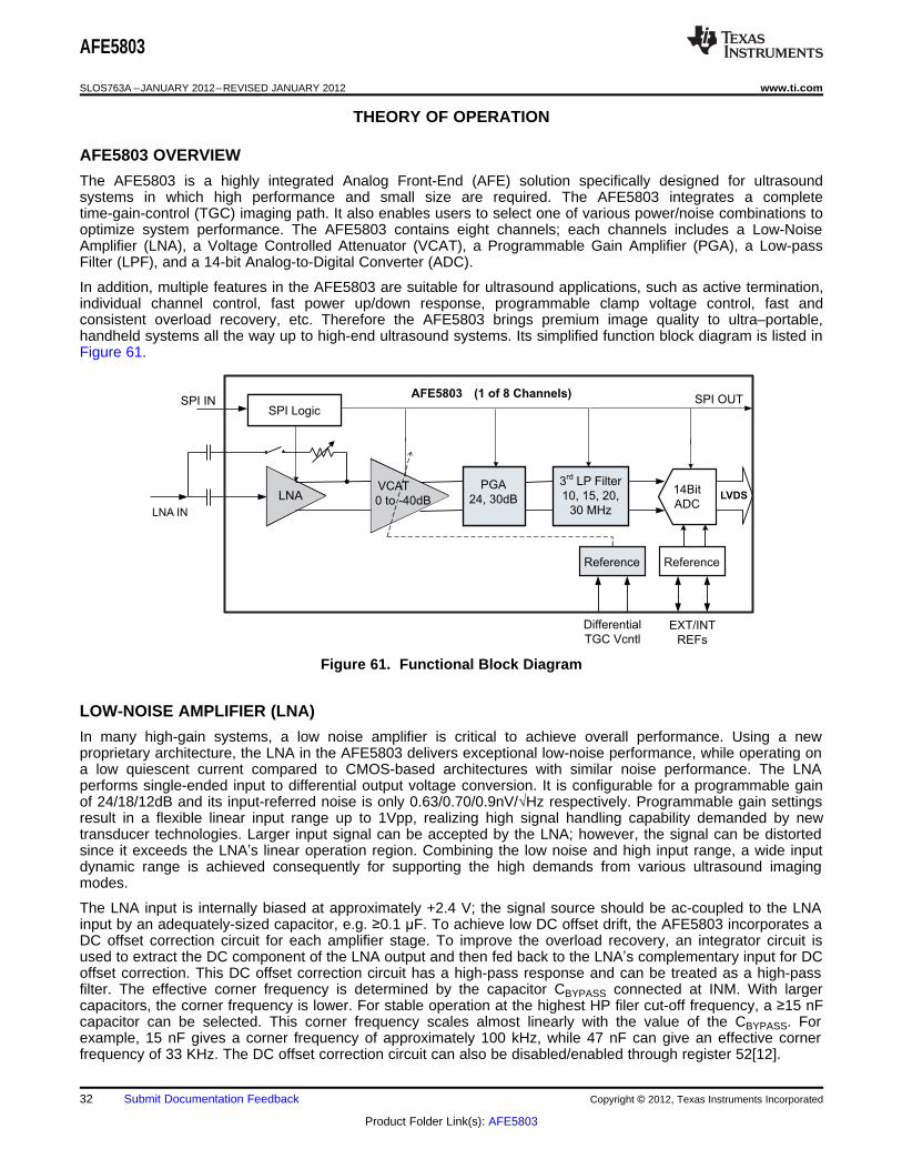
SPI IN
LNA 0 to -40dB
SPI Logic
LNA IN
PGA
24, 30dB
3rd
LP Filter
10, 15, 20,
30 MHz
AFE5803 (1 of 8 Channels)
14Bit
ADCLVDS
ReferenceReference
Differential
TGC VcntlEXT/INT
REFs
SPI OUT
VCAT
AFE5803
SLOS763A –JANUARY 2012–REVISED JANUARY 2012 www.ti.com
THEORY OF OPERATION
AFE5803 OVERVIEW
The AFE5803 is a highly integrated Analog Front-End (AFE) solution specifically designed for ultrasoundsystems in which high performance and small size are required. The AFE5803 integrates a completetime-gain-control (TGC) imaging path. It also enables users to select one of various power/noise combinations tooptimize system performance. The AFE5803 contains eight channels; each channels includes a Low-NoiseAmplifier (LNA), a Voltage Controlled Attenuator (VCAT), a Programmable Gain Amplifier (PGA), a Low-passFilter (LPF), and a 14-bit Analog-to-Digital Converter (ADC).
In addition, multiple features in the AFE5803 are suitable for ultrasound applications, such as active termination,individual channel control, fast power up/down response, programmable clamp voltage control, fast andconsistent overload recovery, etc. Therefore the AFE5803 brings premium image quality to ultra–portable,handheld systems all the way up to high-end ultrasound systems. Its simplified function block diagram is listed inFigure 61.
Figure 61. Functional Block Diagram
LOW-NOISE AMPLIFIER (LNA)
In many high-gain systems, a low noise amplifier is critical to achieve overall performance. Using a newproprietary architecture, the LNA in the AFE5803 delivers exceptional low-noise performance, while operating ona low quiescent current compared to CMOS-based architectures with similar noise performance. The LNAperforms single-ended input to differential output voltage conversion. It is configurable for a programmable gainof 24/18/12dB and its input-referred noise is only 0.63/0.70/0.9nV/√Hz respectively. Programmable gain settingsresult in a flexible linear input range up to 1Vpp, realizing high signal handling capability demanded by newtransducer technologies. Larger input signal can be accepted by the LNA; however, the signal can be distortedsince it exceeds the LNA’s linear operation region. Combining the low noise and high input range, a wide inputdynamic range is achieved consequently for supporting the high demands from various ultrasound imagingmodes.
The LNA input is internally biased at approximately +2.4 V; the signal source should be ac-coupled to the LNAinput by an adequately-sized capacitor, e.g. ≥0.1 µF. To achieve low DC offset drift, the AFE5803 incorporates aDC offset correction circuit for each amplifier stage. To improve the overload recovery, an integrator circuit isused to extract the DC component of the LNA output and then fed back to the LNA’s complementary input for DCoffset correction. This DC offset correction circuit has a high-pass response and can be treated as a high-passfilter. The effective corner frequency is determined by the capacitor CBYPASS connected at INM. With largercapacitors, the corner frequency is lower. For stable operation at the highest HP filer cut-off frequency, a ≥15 nFcapacitor can be selected. This corner frequency scales almost linearly with the value of the CBYPASS. Forexample, 15 nF gives a corner frequency of approximately 100 kHz, while 47 nF can give an effective cornerfrequency of 33 KHz. The DC offset correction circuit can also be disabled/enabled through register 52[12].
32 Submit Documentation Feedback Copyright © 2012, Texas Instruments Incorporated
Product Folder Link(s): AFE5803
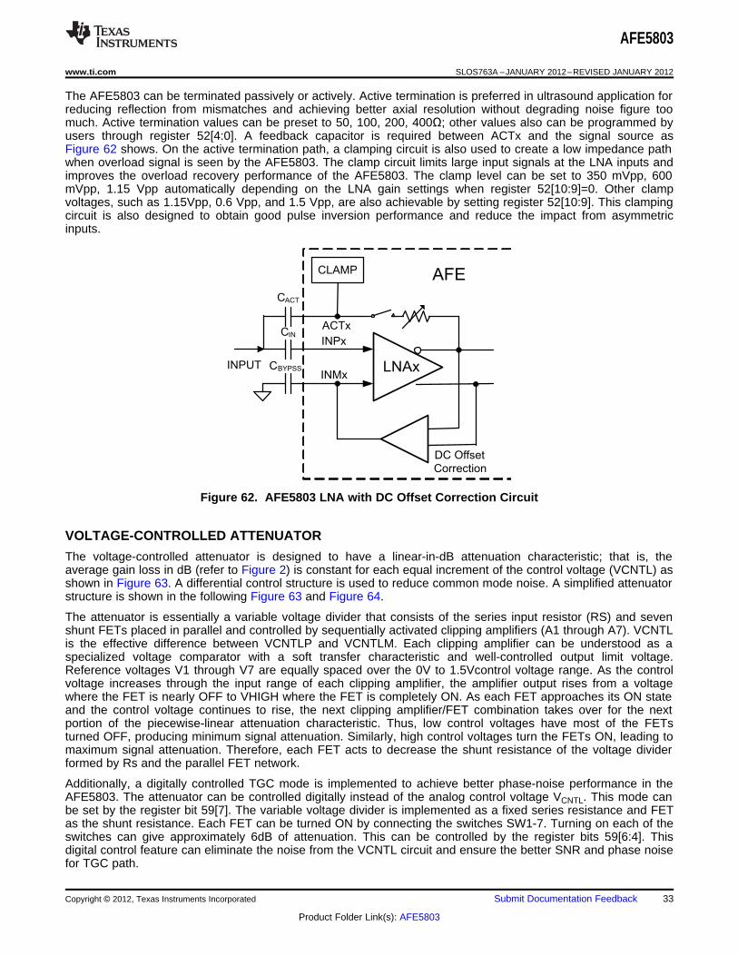
LNAx
INPx
INMx
ACTx
INPUT
AFE
CACT
CIN
CBYPSS
CLAMP
DC Offset
Correction
AFE5803
www.ti.com SLOS763A –JANUARY 2012–REVISED JANUARY 2012
The AFE5803 can be terminated passively or actively. Active termination is preferred in ultrasound application forreducing reflection from mismatches and achieving better axial resolution without degrading noise figure toomuch. Active termination values can be preset to 50, 100, 200, 400Ω; other values also can be programmed byusers through register 52[4:0]. A feedback capacitor is required between ACTx and the signal source asFigure 62 shows. On the active termination path, a clamping circuit is also used to create a low impedance pathwhen overload signal is seen by the AFE5803. The clamp circuit limits large input signals at the LNA inputs andimproves the overload recovery performance of the AFE5803. The clamp level can be set to 350 mVpp, 600mVpp, 1.15 Vpp automatically depending on the LNA gain settings when register 52[10:9]=0. Other clampvoltages, such as 1.15Vpp, 0.6 Vpp, and 1.5 Vpp, are also achievable by setting register 52[10:9]. This clampingcircuit is also designed to obtain good pulse inversion performance and reduce the impact from asymmetricinputs.
Figure 62. AFE5803 LNA with DC Offset Correction Circuit
VOLTAGE-CONTROLLED ATTENUATOR
The voltage-controlled attenuator is designed to have a linear-in-dB attenuation characteristic; that is, theaverage gain loss in dB (refer to Figure 2) is constant for each equal increment of the control voltage (VCNTL) asshown in Figure 63. A differential control structure is used to reduce common mode noise. A simplified attenuatorstructure is shown in the following Figure 63 and Figure 64.
The attenuator is essentially a variable voltage divider that consists of the series input resistor (RS) and sevenshunt FETs placed in parallel and controlled by sequentially activated clipping amplifiers (A1 through A7). VCNTLis the effective difference between VCNTLP and VCNTLM. Each clipping amplifier can be understood as aspecialized voltage comparator with a soft transfer characteristic and well-controlled output limit voltage.Reference voltages V1 through V7 are equally spaced over the 0V to 1.5Vcontrol voltage range. As the controlvoltage increases through the input range of each clipping amplifier, the amplifier output rises from a voltagewhere the FET is nearly OFF to VHIGH where the FET is completely ON. As each FET approaches its ON stateand the control voltage continues to rise, the next clipping amplifier/FET combination takes over for the nextportion of the piecewise-linear attenuation characteristic. Thus, low control voltages have most of the FETsturned OFF, producing minimum signal attenuation. Similarly, high control voltages turn the FETs ON, leading tomaximum signal attenuation. Therefore, each FET acts to decrease the shunt resistance of the voltage dividerformed by Rs and the parallel FET network.
Additionally, a digitally controlled TGC mode is implemented to achieve better phase-noise performance in theAFE5803. The attenuator can be controlled digitally instead of the analog control voltage VCNTL. This mode canbe set by the register bit 59[7]. The variable voltage divider is implemented as a fixed series resistance and FETas the shunt resistance. Each FET can be turned ON by connecting the switches SW1-7. Turning on each of theswitches can give approximately 6dB of attenuation. This can be controlled by the register bits 59[6:4]. Thisdigital control feature can eliminate the noise from the VCNTL circuit and ensure the better SNR and phase noisefor TGC path.
Copyright © 2012, Texas Instruments Incorporated Submit Documentation Feedback 33
Product Folder Link(s): AFE5803

RS
Control
Input
Q1
VB
Q2 Q3
C1
V1
Q4 Q5 Q6 Q7
C2
V2
C3
V3
C4
V4
C5
V5
C6
V6
C7
V7
A1
VCNTL
A1 A1 A1 A1 A1 A1
AttenuatorOutput
C - C Clipping Amplifiers1 8
A1 - A7 Attenuator Stages
AttenuatorInput
RS
Q1
VB
Q2 Q3 Q4 Q5 Q6 Q7
VHIGH
AttenuatorOutput
AttenuatorInput
SW1 SW2 SW3 SW4 SW5 SW6 SW7
AFE5803
SLOS763A –JANUARY 2012–REVISED JANUARY 2012 www.ti.com
Figure 63. Simplified Voltage Controlled Attenuator (Analog Structure)
Figure 64. Simplified Voltage Controlled Attenuator (Digital Structure)
The voltage controlled attenuator’s noise follows a monotonic relationship to the attenuation coefficient. At higherattenuation, the input-referred noise is higher and vice-versa. The attenuator’s noise is then amplified by the PGAand becomes the noise floor at ADC input. In the attenuator’s high attenuation operating range, i.e. VCNTL ishigh, the attenuator’s input noise may exceed the LNA’s output noise; the attenuator then becomes the dominantnoise source for the following PGA stage and ADC. Therefore the attenuator’s noise should be minimizedcompared to the LNA output noise. The AFE5803’s attenuator is designed for achieving low noise even at highattenuation (low channel gain) and realizing better SNR in near field. The input referred noise for differentattenuations is listed in the below table:
Table 8. Voltage-Controlled-Attenuator noise vs Attenuation
Attenuation (dB) Attenuator Input Referred noise (nV/rtHz)
–40 10.5
–36 10
–30 9
–24 8.5
–18 6
–12 4
–6 3
0 2
PROGRAMMABLE GAIN AMPLIFIER (PGA)
After the voltage controlled attenuator, a programmable gain amplifier can be configured as 24dB or 30dB with aconstant input referred noise of 1.75 nV/rtHz. The PGA structure consists of a differential voltage-to-currentconverter with programmable gain, current clamp( bias control) circuits, a transimpedance amplifier with aprogrammable low-pass filter, and a DC offset correction circuit. Its simplified block diagram is shown below:
34 Submit Documentation Feedback Copyright © 2012, Texas Instruments Incorporated
Product Folder Link(s): AFE5803
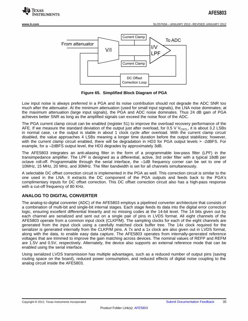
I/V
LPFV/I
Current Clamp
DC Offset
Correction Loop
From attenuatorTo ADC
Current Clamp
AFE5803
www.ti.com SLOS763A –JANUARY 2012–REVISED JANUARY 2012
Figure 65. Simplified Block Diagram of PGA
Low input noise is always preferred in a PGA and its noise contribution should not degrade the ADC SNR toomuch after the attenuator. At the minimum attenuation (used for small input signals), the LNA noise dominates; atthe maximum attenuation (large input signals), the PGA and ADC noise dominates. Thus 24 dB gain of PGAachieves better SNR as long as the amplified signals can exceed the noise floor of the ADC.
The PGA current clamp circuit can be enabled (register 51) to improve the overload recovery performance of theAFE. If we measure the standard deviation of the output just after overload, for 0.5 V VCNTL, it is about 3.2 LSBsin normal case, i.e the output is stable in about 1 clock cycle after overload. With the current clamp circuitdisabled, the value approaches 4 LSBs meaning a longer time duration before the output stabilizes; however,with the current clamp circuit enabled, there will be degradation in HD3 for PGA output levels > -2dBFS. Forexample, for a –2dBFS output level, the HD3 degrades by approximately 3dB.
The AFE5803 integrates an anti-aliasing filter in the form of a programmable low-pass filter (LPF) in thetransimpedance amplifier. The LPF is designed as a differential, active, 3rd order filter with a typical 18dB peroctave roll-off. Programmable through the serial interface, the –1dB frequency corner can be set to one of10MHz, 15 MHz, 20 MHz, and 30MHz. The filter bandwidth is set for all channels simultaneously.
A selectable DC offset correction circuit is implemented in the PGA as well. This correction circuit is similar to theone used in the LNA. It extracts the DC component of the PGA outputs and feeds back to the PGA’scomplimentary inputs for DC offset correction. This DC offset correction circuit also has a high-pass responsewith a cut-off frequency of 80 KHz.
ANALOG TO DIGITAL CONVERTER
The analog-to-digital converter (ADC) of the AFE5803 employs a pipelined converter architecture that consists ofa combination of multi-bit and single-bit internal stages. Each stage feeds its data into the digital error correctionlogic, ensuring excellent differential linearity and no missing codes at the 14-bit level. The 14 bits given out byeach channel are serialized and sent out on a single pair of pins in LVDS format. All eight channels of theAFE5803 operate from a common input clock (CLKP/M). The sampling clocks for each of the eight channels aregenerated from the input clock using a carefully matched clock buffer tree. The 14x clock required for theserializer is generated internally from the CLKP/M pins. A 7x and a 1x clock are also given out in LVDS format,along with the data, to enable easy data capture. The AFE5803 operates from internally-generated referencevoltages that are trimmed to improve the gain matching across devices. The nominal values of REFP and REFMare 1.5V and 0.5V, respectively. Alternately, the device also supports an external reference mode that can beenabled using the serial interface.
Using serialized LVDS transmission has multiple advantages, such as a reduced number of output pins (savingrouting space on the board), reduced power consumption, and reduced effects of digital noise coupling to theanalog circuit inside the AFE5803.
Copyright © 2012, Texas Instruments Incorporated Submit Documentation Feedback 35
Product Folder Link(s): AFE5803

S0492-01
(a) INP (b) INM (c) ACT
CM CM
S0493-01
ADC Input Clocks
CLKP
CLKM
5 kΩ 5 kΩ
VCM
AFE5803
SLOS763A –JANUARY 2012–REVISED JANUARY 2012 www.ti.com
EQUIVALENT CIRCUITS
Figure 66. Equivalent Circuits of LNA inputs
Figure 67. Equivalent Circuits of VCNTLP/M
Figure 68. Equivalent Circuits of Clock Inputs
36 Submit Documentation Feedback Copyright © 2012, Texas Instruments Incorporated
Product Folder Link(s): AFE5803

OUTP
OUTM
Hig
h
Hig
hL
ow
Low
AFE5803
Rout–VdiffVcommon
+Vdiff+
++
–
––
External
100- LoadW
Switch impedance is
nominally 50 ( 10%)W ±
AFE5803
www.ti.com SLOS763A –JANUARY 2012–REVISED JANUARY 2012
Figure 69. Equivalent Circuits of LVDS Outputs
Copyright © 2012, Texas Instruments Incorporated Submit Documentation Feedback 37
Product Folder Link(s): AFE5803

IN CH1
IN CH2
IN CH3
IN CH4
IN CH5
IN CH6
IN CH7
IN CH8
ACT1
ACT2
ACT3
ACT4
ACT5
ACT6
ACT7
ACT8
IN1P
IN2P
IN3P
IN4P
IN5P
IN6P
IN7P
IN8P
IN1M
IN2M
IN3M
IN4M
IN5M
IN6M
IN7M
IN8M
AFE5803
ANALOG INPUTSANALOG OUTPUTS
REF/BIAS DECOUPLINGLVDS OUTPUTS
D1P
D1M
D2P
D2M
D3P
D3M
D4P
D4M
D5P
D5M
D6P
D6M
D7P
D7M
D8P
D8M
DCLKM
DCLKP
FCLKM
FCLKP
REFM
REFP
CLKM
CLKP
AFE5803
CLOCKINPUTS
AFE5803
DIGITALINPUTS
0.1μF
0.1μF
SCLK
SDATA
RESET
SEN
SOUT
PDN_ADC
PDN_VCA
PDN_GLOBAL
AVSS DVSS
AVSS AVSS AVSS DVSS
CVCNTL
470pF
CVCNTL
470pF
CH7_TEST_OUTP
CH7_OUTP
CH7_TEST_OUTM
CH7_BUFFER_OUTM
CH7_BUFFER_OUTP
R (optional)
Clock terminationdepends on clock typesLVDS, PECL, or CMOS
5VA
AV
DD
_5
V
AV
DD
_A
DC
AV
DD
DV
DD
3.3VA 1.8VA 1.8VD10μF
1μF
1μF
1μF
1μF
1μF
1μF
1μF
1μF
>1μF
0.1μF
0.1 μF
0.1μF
0.1μF
0.1μF
0.1μF
0.1μF
0.1μF
0.1μF
15nF
15nF
15nF
15nF
15nF
15nF
15nF
15nF
10μF 10μF 10μF
0.1μF N*0.1 Fμ N*0.1 Fμ N*0.1 Fμ
CM_BYP
VHIGH
VCNTLP INVCNTLP
VCNTLM
VREF_IN
RVCNTL
200Ω
RVCNTL
200Ω
VCNTLM IN
1.4V
>1μFR (optional)
CH7_OUTM
DNCs
CH8_TEST_OUTP
CH8_OUTP
CH8_TEST_OUTM
CH8_BUFFER_OUTM
CH8_BUFFER_OUTP
R (optional)
R (optional)CH8_OUTM
AFE5803
SLOS763A –JANUARY 2012–REVISED JANUARY 2012 www.ti.com
APPLICATION INFORMATION
Figure 70. Application Circuit
38 Submit Documentation Feedback Copyright © 2012, Texas Instruments Incorporated
Product Folder Link(s): AFE5803
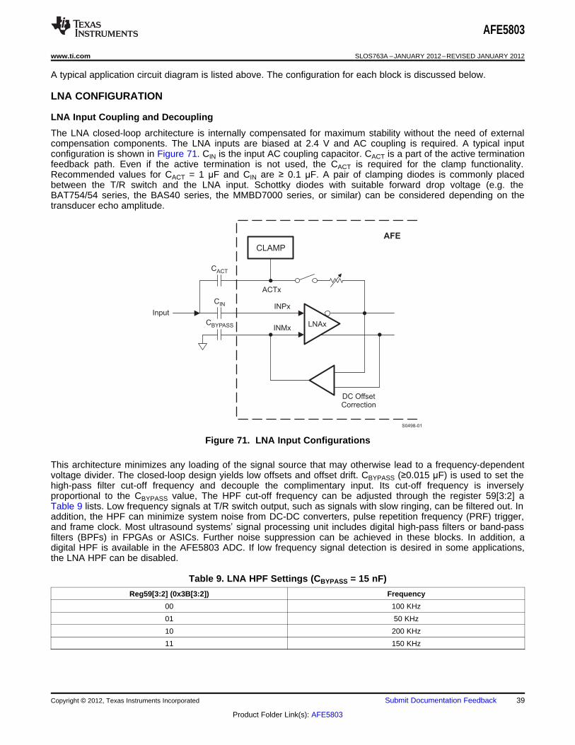
S0498-01
CLAMP
AFE
LNAx
DC OffsetCorrection
ACTx
CACT
CIN
CBYPASS
INPx
INMx
Input
AFE5803
www.ti.com SLOS763A –JANUARY 2012–REVISED JANUARY 2012
A typical application circuit diagram is listed above. The configuration for each block is discussed below.
LNA CONFIGURATION
LNA Input Coupling and Decoupling
The LNA closed-loop architecture is internally compensated for maximum stability without the need of externalcompensation components. The LNA inputs are biased at 2.4 V and AC coupling is required. A typical inputconfiguration is shown in Figure 71. CIN is the input AC coupling capacitor. CACT is a part of the active terminationfeedback path. Even if the active termination is not used, the CACT is required for the clamp functionality.Recommended values for CACT = 1 µF and CIN are ≥ 0.1 µF. A pair of clamping diodes is commonly placedbetween the T/R switch and the LNA input. Schottky diodes with suitable forward drop voltage (e.g. theBAT754/54 series, the BAS40 series, the MMBD7000 series, or similar) can be considered depending on thetransducer echo amplitude.
Figure 71. LNA Input Configurations
This architecture minimizes any loading of the signal source that may otherwise lead to a frequency-dependentvoltage divider. The closed-loop design yields low offsets and offset drift. CBYPASS (≥0.015 µF) is used to set thehigh-pass filter cut-off frequency and decouple the complimentary input. Its cut-off frequency is inverselyproportional to the CBYPASS value, The HPF cut-off frequency can be adjusted through the register 59[3:2] aTable 9 lists. Low frequency signals at T/R switch output, such as signals with slow ringing, can be filtered out. Inaddition, the HPF can minimize system noise from DC-DC converters, pulse repetition frequency (PRF) trigger,and frame clock. Most ultrasound systems’ signal processing unit includes digital high-pass filters or band-passfilters (BPFs) in FPGAs or ASICs. Further noise suppression can be achieved in these blocks. In addition, adigital HPF is available in the AFE5803 ADC. If low frequency signal detection is desired in some applications,the LNA HPF can be disabled.
Table 9. LNA HPF Settings (CBYPASS = 15 nF)
Reg59[3:2] (0x3B[3:2]) Frequency
00 100 KHz
01 50 KHz
10 200 KHz
11 150 KHz
Copyright © 2012, Texas Instruments Incorporated Submit Documentation Feedback 39
Product Folder Link(s): AFE5803
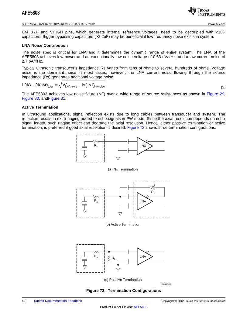
2 2 2
total LNAnoise s LNAnoiseLNA _Noise V R I= + ´
(b) Active Termination
S0499-01
LNARs
(a) No Termination
(c) Passive Termination
LNARs
Rf
LNARs Rt
AFE5803
SLOS763A –JANUARY 2012–REVISED JANUARY 2012 www.ti.com
CM_BYP and VHIGH pins, which generate internal reference voltages, need to be decoupled with ≥1uFcapacitors. Bigger bypassing capacitors (>2.2uF) may be beneficial if low frequency noise exists in system.
LNA Noise Contribution
The noise spec is critical for LNA and it determines the dynamic range of entire system. The LNA of theAFE5803 achieves low power and an exceptionally low-noise voltage of 0.63 nV/√Hz, and a low current noise of2.7 pA/√Hz.
Typical ultrasonic transducer’s impedance Rs varies from tens of ohms to several hundreds of ohms. Voltagenoise is the dominant noise in most cases; however, the LNA current noise flowing through the sourceimpedance (Rs) generates additional voltage noise.
(2)
The AFE5803 achieves low noise figure (NF) over a wide range of source resistances as shown in Figure 29,Figure 30, andFigure 31.
Active Termination
In ultrasound applications, signal reflection exists due to long cables between transducer and system. Thereflection results in extra ringing added to echo signals in PW mode. Since the axial resolution depends on echosignal length, such ringing effect can degrade the axial resolution. Hence, either passive termination or activetermination, is preferred if good axial resolution is desired. Figure 72 shows three termination configurations:
Figure 72. Termination Configurations
40 Submit Documentation Feedback Copyright © 2012, Texas Instruments Incorporated
Product Folder Link(s): AFE5803

S0500-01
AFE
LNAx
ACTx
INPx
INMx
Input
4500Ω
3600Ω
1800Ω
900Ω
450Ω
IN
LNA
RZ
A1
2
=n
+
f
IN IN IN
LNA
RZ / /C / /R
A1
2
=n
+
f
AFE5803
www.ti.com SLOS763A –JANUARY 2012–REVISED JANUARY 2012
Under the no termination configuration, the input impedance of the AFE5803 is about 6 KΩ (8 K//20 pF) at 1MHz. Passive termination requires external termination resistor Rt, which contributes to additional thermal noise.
The LNA supports active termination with programmable values, as shown in Figure 73 .
Figure 73. Active Termination Implementation
The AFE5803 has four pre-settings 50,100, 200 and 400 Ω which are configurable through the registers. Othertermination values can be realized by setting the termination switches shown in Figure 73. Register [52] is usedto enable these switches. The input impedance of the LNA under the active termination configurationapproximately follows:
(3)
Table 5 lists the LNA RINs under different LNA gains. System designers can achieve fine tuning for differentprobes.
The equivalent input impedance is given by Equation 4 where RIN (8 K) and CIN (20 pF) are the input resistanceand capacitance of the LNA.
(4)
Therefore the ZIN is frequency dependent and it decreases as frequency increases shown in Figure 10. Since 2MHz~10 MHz is the most commonly used frequency range in medical ultrasound, this rolling-off effect doesn’timpact system performance greatly. Since each ultrasound system includes multiple transducers with differentimpedances, the flexibility of impedance configuration is a great plus.
Figure 29, Figure 30, and Figure 31 shows the NF under different termination configurations. It indicates that notermination achieves the best noise figure; active termination adds less noise than passive termination. Thustermination topology should be carefully selected based on each use scenario in ultrasound.
Copyright © 2012, Texas Instruments Incorporated Submit Documentation Feedback 41
Product Folder Link(s): AFE5803

W0004-01
(a) Single-Ended Input at VCNTLP
(b) Differential Inputs at V and VCNTLP CNTLM
TGC Gain
V = 0VCNTLM
VCNTLP
1.5V
XdB
X+40dB
TGC Gain
0V
VCNTLM
VCNTLP
XdB
X+40dB
1.5V
0.75V
AFE5803
SLOS763A –JANUARY 2012–REVISED JANUARY 2012 www.ti.com
LNA Gain Switch Response
The LNA gain is programmable through SPI. The gain switching time depends on the SPI speed as well as theLNA gain response time. During the switching, glitches might occur and they can appear as artifacts in images.LNA gain switching in a single imaging line may not be preferred, although digital signal processing might beused here for glitch suppression.
VOLTAGE-CONTROLLED-ATTENUATOR
The attenuator in the AFE5803 is controlled by a pair of differential control inputs, the VCNTLM/P pins. Thedifferential control voltage spans from 0 V to 1.5 V. This control voltage varies the attenuation of the attenuatorbased on its linear-in-dB characteristic. Its maximum attenuation (minimum channel gain) appears at VCNTLP -VCNTLM = 1.5 V, and minimum attenuation (maximum channel gain) occurs at VCNTLP - VCNTLM = 0. The typicalgain range is 40 dB and remains constant, independent of the PGA setting.
When only single-ended VCNTL signal is available, this 1.5 VPP signal can be applied on the VCNTLP pin with theVCNTLM pin connected to ground. As shown in Figure 74, TGC gain curve is inversely proportional to the VCNTLP-VCNTLM.
Figure 74. VCNTLP and VCNTLM Configurations
42 Submit Documentation Feedback Copyright © 2012, Texas Instruments Incorporated
Product Folder Link(s): AFE5803
AFE5803
www.ti.com SLOS763A –JANUARY 2012–REVISED JANUARY 2012
As discussed in the theory of operation, the attenuator architecture uses seven attenuator segments that areequally spaced in order to approximate the linear-in-dB gain-control slope. This approximation results in amonotonic slope; the gain ripple is typically less than ±0.5 dB.
The control voltage input (VCNTLM/P pins) represents a high-impedance input. The VCNTLM/P pins of multipleAFE5803 devices can be connected in parallel with no significant loading effects. When the voltage level (VCNTLP- VCNTLM) is above 1.5 V or below 0 V, the attenuator continues to operate at its maximum attenuation level orminimum attenuation level respectively. It is recommended to limit the voltage from -0.3 V to 2 V.
The AFE5803 gain-control input has a –3 dB bandwidth of approximately 800KHz. This wide bandwidth, althoughuseful in many applications (e.g. fast VCNTL response), can also allow high-frequency noise to modulate the gaincontrol input and finally affect the Doppler performance. In practice, this modulation can be avoided by additionalexternal filtering (RVCNTL and CVCNTL) at VCNTLM/P pins as Figure 69 shows. However, the external filter's cutofffrequency cannot be kept too low as this results in low gain response time. Without external filtering, the gaincontrol response time is typically less than 1 μs to settle within 10% of the final signal level of 1VPP (–6 dBFS)output as indicated in Figure 48 and Figure 49.
Typical VCNTLM/P signals are generated by an 8bit to 12bit 10MSPS digital to analog converter (DAC) and adifferential operation amplifier. TI’s DACs, such as TLV5626 and DAC7821/11 (10 MSPS/12bit), could be used togenerate TGC control waveforms. Differential amplifiers with output common mode voltage control (e.g.THS4130 and OPA1632) can connect the DAC to the VCNTLM/P pins. The buffer amplifier can also be configuredas an active filter to suppress low frequency noise. More information can be found in the documents SLOS318and SBAA150. The VCNTL vs Gain curves can be found in Figure 2. The below table also shows the absolutegain vs. VCNTL, which may help program DAC correspondingly.
In PW Doppler and color Doppler modes, VCNTL noise should be minimized to achieve the best close-in phasenoise and SNR. Digital VCNTL feature is implemented to address this need in the AFE5803. In the digital VCNTLmode, no external VCNTL is needed.
Table 10. VCNTLP–VCNTLM vs Gain Under Different LNA and PGA Gain Settings (Low Noise Mode)
Gain (dB) Gain (dB) Gain (dB) Gain (dB) Gain (dB) Gain (dB)VCNTLP–VCNTLM LNA = 12 dB LNA = 18 dB LNA = 24 dB LNA = 12 dB LNA = 18 dB LNA = 24 dB(V) PGA = 24 dB PGA = 24 dB PGA = 24 dB PGA = 30 dB PGA = 30 dB PGA = 30 dB
0 36.45 42.45 48.45 42.25 48.25 54.25
0.1 33.91 39.91 45.91 39.71 45.71 51.71
0.2 30.78 36.78 42.78 36.58 42.58 48.58
0.3 27.39 33.39 39.39 33.19 39.19 45.19
0.4 23.74 29.74 35.74 29.54 35.54 41.54
0.5 20.69 26.69 32.69 26.49 32.49 38.49
0.6 17.11 23.11 29.11 22.91 28.91 34.91
0.7 13.54 19.54 25.54 19.34 25.34 31.34
0.8 10.27 16.27 22.27 16.07 22.07 28.07
0.9 6.48 12.48 18.48 12.28 18.28 24.28
1.0 3.16 9.16 15.16 8.96 14.96 20.96
1.1 –0.35 5.65 11.65 5.45 11.45 17.45
1.2 –2.48 3.52 9.52 3.32 9.32 15.32
1.3 –3.58 2.42 8.42 2.22 8.22 14.22
1.4 –4.01 1.99 7.99 1.79 7.79 13.79
1.5 –4 2 8 1.8 7.8 13.8
Copyright © 2012, Texas Instruments Incorporated Submit Documentation Feedback 43
Product Folder Link(s): AFE5803

FPGA Clock/Noisy Clock
n×(20~65)MHz
TI Jitter CleanerCDCE72010/CDCM7005
CDCLVP12081-to-8
CLK Buffer
20~65 MHzADC CLK
8 SynchronizedADC CLKs
CDCE72010 has 10outputs thus the buffermay not be needed for64CH systems
AF
E
AF
E
AF
E
AF
E
AF
E
AF
E
AF
E
AF
E
B0437-01
AFE5803
SLOS763A –JANUARY 2012–REVISED JANUARY 2012 www.ti.com
ADC OPERATION
ADC Clock Distribution
To ensure that the aperture delay and jitter are the same for all channels, the AFE5803 uses a clock treenetwork to generate individual sampling clocks for each channel. The clock, for all the channels, are matchedfrom the source point to the sampling circuit of each of the eight internal ADCs. The variation on this delay isdescribed in the aperture delay parameter of the output interface timing. Its variation is given by the aperture jitternumber of the same table.
Figure 75. ADC Clock Distribution Network
In the single-end case, it is recommended that the use of low jitter square signals (LVCMOS levels, 1.8 Vamplitude). See TI document SLYT075 for further details on the theory.
The jitter cleaner CDCM7005 or CDCE72010 is suitable to generate the AFE5803’s ADC clock and ensure theperformance for the14 bit ADC with 77 dBFS SNR. A clock distribution network is shown in Figure 75.
The AFE5803 can accept differential LVDS, LVPECL, and other differential clock inputs as well as single-endedclock. AC coupling is required between clock drivers and the AFE5803 clock inputs. When single-ended clock isused, CLKM should be tied to ground. Common clock configurations are illustrated in Figure 76. Appropriatetermination is recommended to achieve good signal integrity.
44 Submit Documentation Feedback Copyright © 2012, Texas Instruments Incorporated
Product Folder Link(s): AFE5803
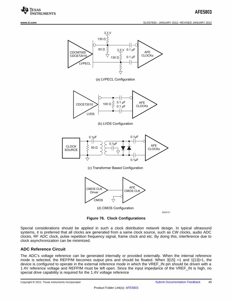
S0503-01
(a) LVPECL Configuration
(c) Transformer Based Configuration
(d) CMOS Configuration
(b) LVDS Configuration
CMOS CLKDriver
AFECMOS CLK
CMOS
AFECLOCKs
CLOCKSOURCE
50 Ω
0.1 Fμ
0.1 Fμ
0.1 Fμ
0.1 Fμ
CDCE72010AFE
CLOCKs100 Ω
LVDS
0.1 Fμ
0.1 Fμ
CDCM7005CDCE72010
AFECLOCKs
130 Ω
LVPECL
0.1 Fμ
0.1 Fμ
83 Ω 3.3 V
3.3 V
130 Ω
AFE5803
www.ti.com SLOS763A –JANUARY 2012–REVISED JANUARY 2012
Figure 76. Clock Configurations
Special considerations should be applied in such a clock distribution network design. In typical ultrasoundsystems, it is preferred that all clocks are generated from a same clock source, such as CW clocks, audio ADCclocks, RF ADC clock, pulse repetition frequency signal, frame clock and etc. By doing this, interference due toclock asynchronization can be minimized.
ADC Reference Circuit
The ADC’s voltage reference can be generated internally or provided externally. When the internal referencemode is selected, the REFP/M becomes output pins and should be floated. When 3[15] =1 and 1[13]=1, thedevice is configured to operate in the external reference mode in which the VREF_IN pin should be driven with a1.4V reference voltage and REFP/M must be left open. Since the input impedance of the VREF_IN is high, nospecial drive capability is required for the 1.4V voltage reference
Copyright © 2012, Texas Instruments Incorporated Submit Documentation Feedback 45
Product Folder Link(s): AFE5803

AFE5803
SLOS763A –JANUARY 2012–REVISED JANUARY 2012 www.ti.com
The digital beam-forming algorithm in an ultrasound system relies on gain matching across all receiver channels.A typical system would have about 12 octal AFEs on the board. In such a case, it is critical to ensure that thegain is matched, essentially requiring the reference voltages seen by all the AFEs to be the same. Matchingreferences within the eight channels of a chip is done by using a single internal reference voltage buffer.Trimming the reference voltages on each chip during production ensures that the reference voltages arewell-matched across different chips. When the external reference mode is used, a solid reference plane on aprinted circuit board can ensure minimal voltage variation across devices. More information on voltage referencedesign can be found in the document SLYT339. The dominant gain variation in the AFE5803 comes from theVCA gain variation. The gain variation contributed by the ADC reference circuit is much smaller than the VCAgain variation. Hence, in most systems, using the ADC internal reference mode is sufficient to maintain good gainmatching among multiple AFE5803s. In addition, the internal reference circuit without any external componentsachieves satisfactory thermal noise and phase noise performance.
POWER MANAGEMENT
Power/Performance Optimization
The AFE5803 has options to adjust power consumption and meet different noise performances. This featurewould be useful for portable systems operated by batteries when low power is more desired. See the electricalcharacteristics table as well as the typical characteristic plots.
Power Management Priority
Power management plays a critical role to extend battery life and ensure long operation time. The AFE5803 hasfast and flexible power down/up control which can maximize battery life. The AFE5803 can be powered down/upthrough external pins or internal registers. The following table indicates the affected circuit blocks and prioritieswhen the power management is invoked. The higher priority controls can overwrite the lower priority ones.In thedevice, all the power down controls are logically ORed to generate final power down for different blocks. Thus,the higher priority controls can cover the lower priority ones. The AFE5803 register settings are maintained whenthe AFE5803 is in either partial power down mode or complete power down mode.
Table 11. Power Management Priority
Name Blocks Priority
Pin PDN_GLOBAL All High
Pin PDN_VCA LNA + VCAT+ PGA Medium
Register VCA_PARTIAL_PDN LNA + VCAT+ PGA Low
Register VCA_COMPLETE_PDN LNA + VCAT+ PGA Medium
Pin PDN_ADC ADC Medium
Register ADC_PARTIAL_PDN ADC Low
Register ADC_COMPLETE_PDN ADC Medium
Register PDN_VCAT_PGA VCAT + PGA Lowest
Register PDN_LNA LNA Lowest
Partial Power-Up/Down Mode
The partial power up/down mode is also called as fast power up/down mode. In this mode, most amplifiers in thesignal path are powered down, while the internal reference circuits remain active as well as the LVDS clockcircuit, i.e. the LVDS circuit still generates its frame and bit clocks.
The partial power down function allows the AFE5803 to be wake up from a low-power state quickly. Thisconfiguration ensures that the external capacitors are discharged slowly; thus a minimum wake-up time isneeded as long as the charges on those capacitors are restored. The VCA wake-up response is typically about 2μs or 1% of the power down duration whichever is larger. The longest wake-up time depends on the capacitorsconnected at INP and INM, as the wake-up time is the time required to recharge the caps to the desiredoperating voltages. For 0.1μF at INP and 15nF at INM can give a wake-up time of 2.5ms. For larger capacitorsthis time will be longer. The ADC wake-up time is about 1 μs. Thus the AFE5803 wake-up time is moredependent on the VCA wake-up time. This also assumes that the ADC clock has been running for at least 50 µsbefore normal operating mode resumes. The power-down time is instantaneous, less than 1.0µs.
46 Submit Documentation Feedback Copyright © 2012, Texas Instruments Incorporated
Product Folder Link(s): AFE5803

Buffer
Amp
Rint/Rext
Rint/RextCH7/8_BUFFER_OUTM
CH7/8_BUFFER_OUTP
CH7/8_TEST_OUTM
CH7/8_TEST_OUTPPGA CH7/8P
PGA CH7/8M
5 kW
5 kW
AFE5803
www.ti.com SLOS763A –JANUARY 2012–REVISED JANUARY 2012
This fast wake-up response is desired for portable ultrasound applications in which the power saving is critical.The pulse repetition frequency of a ultrasound system could vary from 50KHz to 500Hz, while the imaging depth(i.e., the active period for a receive path) varies from 10 μs to hundreds of us. The power saving can be prettysignificant when a system’s PRF is low. In some cases, only the VCA would be powered down while the ADCkeeps running normally to ensure minimal impact to FPGAs.
In the partial power-down mode, the AFE5803 typically dissipates only 26mW/ch, representing an 80% powerreduction compared to the normal operating mode. This mode can be set using either pins (PDN_VCA andPDN_ADC) or register bits (VCA_PARTIAL_PDN and ADC_PARTIAL_PDN).
Complete Power-Down Mode
To achieve the lowest power dissipation of 0.7 mW/CH, the AFE5803 can be placed into a complete power-downmode. This mode is controlled through the registers ADC_COMPLETE_PDN, VCA_COMPLETE_PDN orPDN_GLOBAL pin. In the complete power-down mode, all circuits including reference circuits within theAFE5803 are powered down; and the capacitors connected to the AFE5803 are discharged. The wake-up timedepends on the time needed to recharge these capacitors. The wake-up time depends on the time that theAFE5803 spends in shutdown mode. 0.1μF at INP and 15 nF at INM can give a wake-up time close to 2.5ms.
VCA TEST MODES
The AFE5803 includes multiple test modes to accelerate system development. The ADC test modes have beendiscussed in the register description section.
The VCA has a test mode in which the CH7 and CH8 PGA outputs can be brought. By monitoring these PGAoutputs, the functionality of VCA operation can be verified. Some registers are related to this test mode. PGATest Mode Enable: Reg59[9]; Buffer Amplifier Power Down Reg59[8]; and Buffer Amplifier Gain ControlReg54[4:0].
The PGA outputs are connected to the virtual ground pins of the buffer amplifier through 5 kΩ resistors. The PGAoutputs can be monitored at the buffer amplifier outputs when the buffer amplifer is enabled. Note that thesignals at the buffer amplifier outputs are attenuated due to the 5KΩ resistors. The attenuation coefficient isRINT/EXT/5kΩ. See Table 7 for the RINT configuration.
An alternative way is to measure the PGA outputs directly at the CH8_TEST_OUTM/P and CH7_TEST_OUTM/Pwhen the buffer amplifier is powered down.
Based on the buffer amplifier configuration, the registers can be set in different ways:
Configuration 1:In this configuration, the test outputs can be monitored at CH7/8_TEST_OUTP/M
Reg59[9]=1 ;Test mode enabledReg59[8]=0 ;Buffer amplifier powered down
Configuration 2:In this configuration, the test outputs can be monitored at CH7/8_BUFFER_OUTP/M
Reg59[9]=1 ;Test mode enabledReg59[8]=1 ;Buffer amplifier powered onReg54[4:0]=10H; Internal feedback 2K resistor enabled. Different values can be used as well
Figure 77. AFE5803 PGA Test Mode
Copyright © 2012, Texas Instruments Incorporated Submit Documentation Feedback 47
Product Folder Link(s): AFE5803
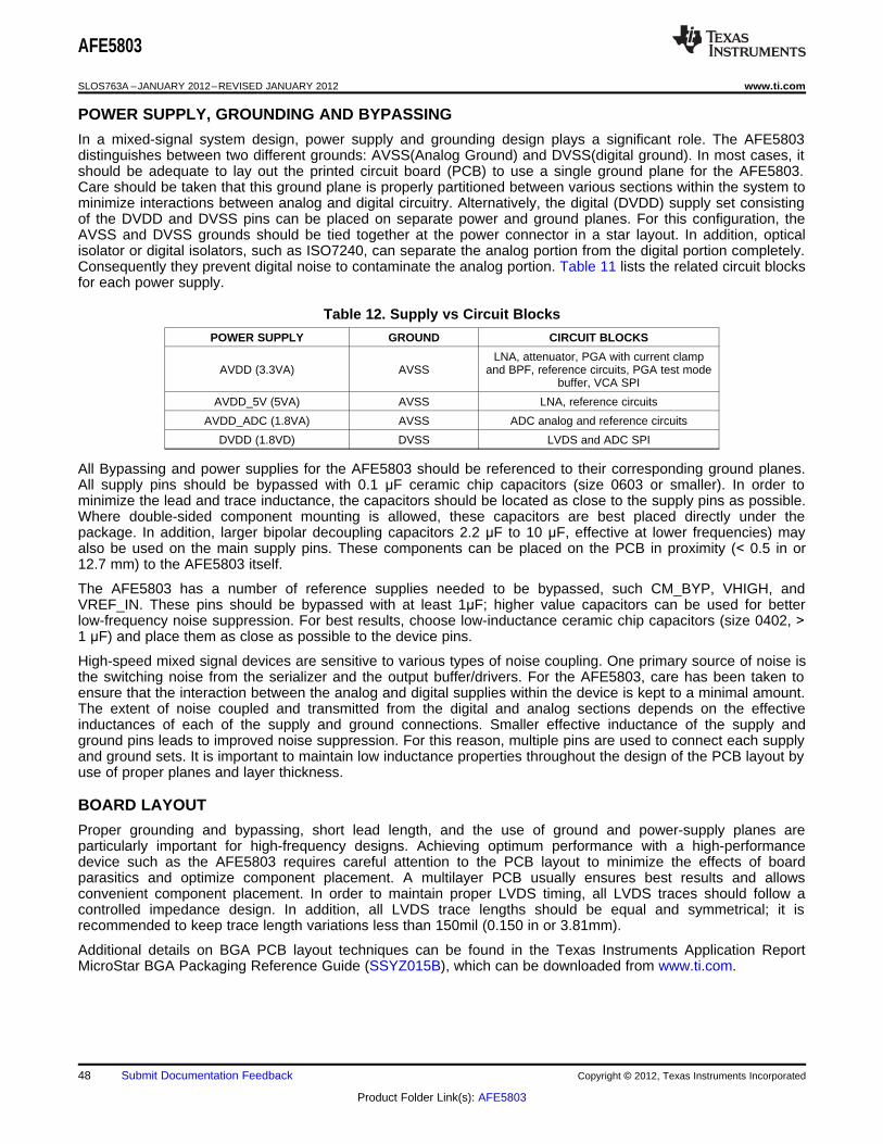
AFE5803
SLOS763A –JANUARY 2012–REVISED JANUARY 2012 www.ti.com
POWER SUPPLY, GROUNDING AND BYPASSING
In a mixed-signal system design, power supply and grounding design plays a significant role. The AFE5803distinguishes between two different grounds: AVSS(Analog Ground) and DVSS(digital ground). In most cases, itshould be adequate to lay out the printed circuit board (PCB) to use a single ground plane for the AFE5803.Care should be taken that this ground plane is properly partitioned between various sections within the system tominimize interactions between analog and digital circuitry. Alternatively, the digital (DVDD) supply set consistingof the DVDD and DVSS pins can be placed on separate power and ground planes. For this configuration, theAVSS and DVSS grounds should be tied together at the power connector in a star layout. In addition, opticalisolator or digital isolators, such as ISO7240, can separate the analog portion from the digital portion completely.Consequently they prevent digital noise to contaminate the analog portion. Table 11 lists the related circuit blocksfor each power supply.
Table 12. Supply vs Circuit Blocks
POWER SUPPLY GROUND CIRCUIT BLOCKS
LNA, attenuator, PGA with current clampAVDD (3.3VA) AVSS and BPF, reference circuits, PGA test mode
buffer, VCA SPI
AVDD_5V (5VA) AVSS LNA, reference circuits
AVDD_ADC (1.8VA) AVSS ADC analog and reference circuits
DVDD (1.8VD) DVSS LVDS and ADC SPI
All Bypassing and power supplies for the AFE5803 should be referenced to their corresponding ground planes.All supply pins should be bypassed with 0.1 µF ceramic chip capacitors (size 0603 or smaller). In order tominimize the lead and trace inductance, the capacitors should be located as close to the supply pins as possible.Where double-sided component mounting is allowed, these capacitors are best placed directly under thepackage. In addition, larger bipolar decoupling capacitors 2.2 µF to 10 µF, effective at lower frequencies) mayalso be used on the main supply pins. These components can be placed on the PCB in proximity (< 0.5 in or12.7 mm) to the AFE5803 itself.
The AFE5803 has a number of reference supplies needed to be bypassed, such CM_BYP, VHIGH, andVREF_IN. These pins should be bypassed with at least 1µF; higher value capacitors can be used for betterlow-frequency noise suppression. For best results, choose low-inductance ceramic chip capacitors (size 0402, >1 µF) and place them as close as possible to the device pins.
High-speed mixed signal devices are sensitive to various types of noise coupling. One primary source of noise isthe switching noise from the serializer and the output buffer/drivers. For the AFE5803, care has been taken toensure that the interaction between the analog and digital supplies within the device is kept to a minimal amount.The extent of noise coupled and transmitted from the digital and analog sections depends on the effectiveinductances of each of the supply and ground connections. Smaller effective inductance of the supply andground pins leads to improved noise suppression. For this reason, multiple pins are used to connect each supplyand ground sets. It is important to maintain low inductance properties throughout the design of the PCB layout byuse of proper planes and layer thickness.
BOARD LAYOUT
Proper grounding and bypassing, short lead length, and the use of ground and power-supply planes areparticularly important for high-frequency designs. Achieving optimum performance with a high-performancedevice such as the AFE5803 requires careful attention to the PCB layout to minimize the effects of boardparasitics and optimize component placement. A multilayer PCB usually ensures best results and allowsconvenient component placement. In order to maintain proper LVDS timing, all LVDS traces should follow acontrolled impedance design. In addition, all LVDS trace lengths should be equal and symmetrical; it isrecommended to keep trace length variations less than 150mil (0.150 in or 3.81mm).
Additional details on BGA PCB layout techniques can be found in the Texas Instruments Application ReportMicroStar BGA Packaging Reference Guide (SSYZ015B), which can be downloaded from www.ti.com.
48 Submit Documentation Feedback Copyright © 2012, Texas Instruments Incorporated
Product Folder Link(s): AFE5803

AFE5803
www.ti.com SLOS763A –JANUARY 2012–REVISED JANUARY 2012
REVISION HISTORY
Changes from Original (January 2012) to Revision A Page
• Changed Table 3 Digital HPF –1dB Corner Frequency vs K and Fs ................................................................................. 27
Copyright © 2012, Texas Instruments Incorporated Submit Documentation Feedback 49
Product Folder Link(s): AFE5803
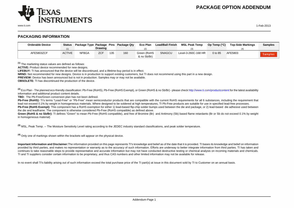
PACKAGE OPTION ADDENDUM
www.ti.com 1-Feb-2013
Addendum-Page 1
PACKAGING INFORMATION
Orderable Device Status(1)
Package Type PackageDrawing
Pins Package Qty Eco Plan(2)
Lead/Ball Finish MSL Peak Temp(3)
Op Temp (°C) Top-Side Markings(4)
Samples
AFE5803ZCF ACTIVE NFBGA ZCF 135 160 Green (RoHS& no Sb/Br)
SNAGCU Level-3-260C-168 HR 0 to 85 AFE5803
(1) The marketing status values are defined as follows:ACTIVE: Product device recommended for new designs.LIFEBUY: TI has announced that the device will be discontinued, and a lifetime-buy period is in effect.NRND: Not recommended for new designs. Device is in production to support existing customers, but TI does not recommend using this part in a new design.PREVIEW: Device has been announced but is not in production. Samples may or may not be available.OBSOLETE: TI has discontinued the production of the device.
(2) Eco Plan - The planned eco-friendly classification: Pb-Free (RoHS), Pb-Free (RoHS Exempt), or Green (RoHS & no Sb/Br) - please check http://www.ti.com/productcontent for the latest availabilityinformation and additional product content details.TBD: The Pb-Free/Green conversion plan has not been defined.Pb-Free (RoHS): TI's terms "Lead-Free" or "Pb-Free" mean semiconductor products that are compatible with the current RoHS requirements for all 6 substances, including the requirement thatlead not exceed 0.1% by weight in homogeneous materials. Where designed to be soldered at high temperatures, TI Pb-Free products are suitable for use in specified lead-free processes.Pb-Free (RoHS Exempt): This component has a RoHS exemption for either 1) lead-based flip-chip solder bumps used between the die and package, or 2) lead-based die adhesive used betweenthe die and leadframe. The component is otherwise considered Pb-Free (RoHS compatible) as defined above.Green (RoHS & no Sb/Br): TI defines "Green" to mean Pb-Free (RoHS compatible), and free of Bromine (Br) and Antimony (Sb) based flame retardants (Br or Sb do not exceed 0.1% by weightin homogeneous material)
(3) MSL, Peak Temp. -- The Moisture Sensitivity Level rating according to the JEDEC industry standard classifications, and peak solder temperature.
(4) Only one of markings shown within the brackets will appear on the physical device.
Important Information and Disclaimer:The information provided on this page represents TI's knowledge and belief as of the date that it is provided. TI bases its knowledge and belief on informationprovided by third parties, and makes no representation or warranty as to the accuracy of such information. Efforts are underway to better integrate information from third parties. TI has taken andcontinues to take reasonable steps to provide representative and accurate information but may not have conducted destructive testing or chemical analysis on incoming materials and chemicals.TI and TI suppliers consider certain information to be proprietary, and thus CAS numbers and other limited information may not be available for release.
In no event shall TI's liability arising out of such information exceed the total purchase price of the TI part(s) at issue in this document sold by TI to Customer on an annual basis.


IMPORTANT NOTICE
Texas Instruments Incorporated and its subsidiaries (TI) reserve the right to make corrections, enhancements, improvements and otherchanges to its semiconductor products and services per JESD46, latest issue, and to discontinue any product or service per JESD48, latestissue. Buyers should obtain the latest relevant information before placing orders and should verify that such information is current andcomplete. All semiconductor products (also referred to herein as “components”) are sold subject to TI’s terms and conditions of salesupplied at the time of order acknowledgment.
TI warrants performance of its components to the specifications applicable at the time of sale, in accordance with the warranty in TI’s termsand conditions of sale of semiconductor products. Testing and other quality control techniques are used to the extent TI deems necessaryto support this warranty. Except where mandated by applicable law, testing of all parameters of each component is not necessarilyperformed.
TI assumes no liability for applications assistance or the design of Buyers’ products. Buyers are responsible for their products andapplications using TI components. To minimize the risks associated with Buyers’ products and applications, Buyers should provideadequate design and operating safeguards.
TI does not warrant or represent that any license, either express or implied, is granted under any patent right, copyright, mask work right, orother intellectual property right relating to any combination, machine, or process in which TI components or services are used. Informationpublished by TI regarding third-party products or services does not constitute a license to use such products or services or a warranty orendorsement thereof. Use of such information may require a license from a third party under the patents or other intellectual property of thethird party, or a license from TI under the patents or other intellectual property of TI.
Reproduction of significant portions of TI information in TI data books or data sheets is permissible only if reproduction is without alterationand is accompanied by all associated warranties, conditions, limitations, and notices. TI is not responsible or liable for such altereddocumentation. Information of third parties may be subject to additional restrictions.
Resale of TI components or services with statements different from or beyond the parameters stated by TI for that component or servicevoids all express and any implied warranties for the associated TI component or service and is an unfair and deceptive business practice.TI is not responsible or liable for any such statements.
Buyer acknowledges and agrees that it is solely responsible for compliance with all legal, regulatory and safety-related requirementsconcerning its products, and any use of TI components in its applications, notwithstanding any applications-related information or supportthat may be provided by TI. Buyer represents and agrees that it has all the necessary expertise to create and implement safeguards whichanticipate dangerous consequences of failures, monitor failures and their consequences, lessen the likelihood of failures that might causeharm and take appropriate remedial actions. Buyer will fully indemnify TI and its representatives against any damages arising out of the useof any TI components in safety-critical applications.
In some cases, TI components may be promoted specifically to facilitate safety-related applications. With such components, TI’s goal is tohelp enable customers to design and create their own end-product solutions that meet applicable functional safety standards andrequirements. Nonetheless, such components are subject to these terms.
No TI components are authorized for use in FDA Class III (or similar life-critical medical equipment) unless authorized officers of the partieshave executed a special agreement specifically governing such use.
Only those TI components which TI has specifically designated as military grade or “enhanced plastic” are designed and intended for use inmilitary/aerospace applications or environments. Buyer acknowledges and agrees that any military or aerospace use of TI componentswhich have not been so designated is solely at the Buyer's risk, and that Buyer is solely responsible for compliance with all legal andregulatory requirements in connection with such use.
TI has specifically designated certain components as meeting ISO/TS16949 requirements, mainly for automotive use. In any case of use ofnon-designated products, TI will not be responsible for any failure to meet ISO/TS16949.
Products Applications
Audio www.ti.com/audio Automotive and Transportation www.ti.com/automotive
Amplifiers amplifier.ti.com Communications and Telecom www.ti.com/communications
Data Converters dataconverter.ti.com Computers and Peripherals www.ti.com/computers
DLP® Products www.dlp.com Consumer Electronics www.ti.com/consumer-apps
DSP dsp.ti.com Energy and Lighting www.ti.com/energy
Clocks and Timers www.ti.com/clocks Industrial www.ti.com/industrial
Interface interface.ti.com Medical www.ti.com/medical
Logic logic.ti.com Security www.ti.com/security
Power Mgmt power.ti.com Space, Avionics and Defense www.ti.com/space-avionics-defense
Microcontrollers microcontroller.ti.com Video and Imaging www.ti.com/video
RFID www.ti-rfid.com
OMAP Applications Processors www.ti.com/omap TI E2E Community e2e.ti.com
Wireless Connectivity www.ti.com/wirelessconnectivity
Mailing Address: Texas Instruments, Post Office Box 655303, Dallas, Texas 75265Copyright © 2013, Texas Instruments Incorporated