FT2232H Used in an FT245 Style Synchronous FIFO · PDF file · 2016-07-25AN_130...
20
Use of FTDI devices in life support and/or safety applications is entirely at the user’s risk, and the user agrees to defend, indemnify and hold FTDI harmless from any and all damages, claims, suits or expense resulting from such use. Future Technology Devices International Limited (FTDI) Unit 1,2 Seaward Place, Glasgow G41 1HH, United Kingdom Tel.: +44 (0) 141 429 2777 Fax: + 44 (0) 141 429 2758 E-Mail (Support): [email protected] Web: http://www.ftdichip.com Copyright © 2015 Future Technology Devices International Limited Application Note AN_130 FT2232H Used in an FT245 Style Synchronous FIFO Mode Version 1.3 Issue Date: 2015-11-17 This application note describes how to use the FT2232H device in FT245 Style Synchronous FIFO mode
Transcript of FT2232H Used in an FT245 Style Synchronous FIFO · PDF file · 2016-07-25AN_130...
Use of FTDI devices in life support and/or safety applications is entirely at the user’s risk, and the user agrees to defend, indemnify and hold FTDI harmless from any and all damages, claims, suits or expense
resulting from such use.
Future Technology Devices International Limited (FTDI)
Unit 1,2 Seaward Place, Glasgow G41 1HH, United Kingdom Tel.: +44 (0) 141 429 2777 Fax: + 44 (0) 141 429 2758
E-Mail (Support): [email protected] Web: http://www.ftdichip.com
Copyright © 2015 Future Technology Devices International Limited
Application Note
AN_130
FT2232H Used in an FT245 Style
Synchronous FIFO Mode
Version 1.3
Issue Date: 2015-11-17
This application note describes how to use the FT2232H device in FT245 Style Synchronous FIFO mode

1 P roduc t Page
Document Feedback C opyright © 2015 Future Technology Devices International Limited
Application Note
AN_130 FT2232H Used in an FT245 Style Synchronous FIFO Mode V ers ion 1 .3
Document Reference No.: FT_000186 C learance No.: FTDI# 117
Table of Contents
1 Introduction ................................................................. 2
2 Hardware Configuration ................................................ 3
2.1 Pin Assignment under Synchronous FIFO Interface ................. 4
2.2 IO Timing .............................................................................. 5
3 Software Configuration ................................................. 7
3.1 EEPROM Setting ..................................................................... 8
4 Application Development............................................... 9
4.1 Code example .......................................................................10
4.2 Getting The Best Performance ...............................................11
4.3 Write Data Mode ...................................................................14
4.4 Read Data Mode ....................................................................15
5 Contact Information .................................................... 16
Appendix A – References ................................................. 17
Document References ...................................................................17
Acronyms and Abbreviations .........................................................17
Appendix B – List of Tables & Figures ............................... 18
List of Tables ................................................................................18
List of Figures ...............................................................................18
Appendix C– Revision History........................................... 19
2 P roduc t Page
Document Feedback C opyright © 2015 Future Technology Devices International Limited
Application Note
AN_130 FT2232H Used in an FT245 Style Synchronous FIFO Mode V ers ion 1 .3
Document Reference No.: FT_000186 C learance No.: FTDI# 117
1 Introduction
This application note illustrates how to set the FT2232H into an FT245 Style Synchronous FIFO mode. If
the requirement is to transfer data at 60MHz, and the data rate must greater than 8MB per second, then
the FT245 Style Synchronous FIFO mode is the best solution.
The FT2232H only channel A can be configured as a FT245 style synchronous FIFO interface . When Configured in this mode, channel B is not available as all resources have been switched onto channel A.
Note: This mode is only available with port A of FT2232H device.

3 P roduc t Page
Document Feedback C opyright © 2015 Future Technology Devices International Limited
Application Note
AN_130 FT2232H Used in an FT245 Style Synchronous FIFO Mode V ers ion 1 .3
Document Reference No.: FT_000186 C learance No.: FTDI# 117
2 Hardware Configuration
EEPROM Configuration:
The FT2232H device requires an external 93C46 EEPROM organized in 16-bit words. It also supports the
93C56 and 93C66 EEPROMs organized in 16-bit words.
Device connection setting:
Use a USB cable to connect an FT2232H device to a PC - the pin assignment in Table 1 - Channel A
FT245 Style Synchronous FIFO Configured Pin Descriptions
give details of the required connection between the system and FT2232H.
4 P roduc t Page
Document Feedback C opyright © 2015 Future Technology Devices International Limited
Application Note
AN_130 FT2232H Used in an FT245 Style Synchronous FIFO Mode V ers ion 1 .3
Document Reference No.: FT_000186 C learance No.: FTDI# 117
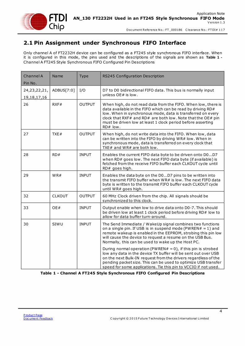
2.1 Pin Assignment under Synchronous FIFO Interface
Only channel A of FT2232H device can be configured as a FT245 style synchronous FIFO interface. When it is configured in this mode, the pins used and the descriptions of the signals are shown as Table 1 -
Channel A FT245 Style Synchronous FIFO Configured Pin Descriptions
Channel A
Pin No.
Name Type RS245 Configuration Description
24,23,22,21,
19,18,17,16
ADBUS[7:0] I/O D7 to D0 bidirectional FIFO data. This bus is normally input
unless OE# is low.
26 RXF# OUTPUT When high, do not read data from the FIFO. When low, there is
data available in the FIFO which can be read by driving RD# low. When in synchronous mode, data is transferred on every
clock that RXF# and RD# are both low. Note that the OE# pin must be driven low at least 1 clock period before asserting
RD# low.
27 TXE# OUTPUT When high, do not write data into the FIFO. When low, data
can be written into the FIFO by driving WR# low. When in synchronous mode, data is transferred on every clock that
TXE# and WR# are both low.
28 RD# INPUT Enables the current FIFO data byte to be driven onto D0...D7
when RD# goes low. The next FIFO data byte (if available) is fetched from the receive FIFO buffer each CLKOUT cycle until
RD# goes high.
29 WR# INPUT Enables the data byte on the D0...D7 pins to be written into
the transmit FIFO buffer when WR# is low. The next FIFO data byte is written to the transmit FIFO buffer each CLKOUT cycle
until WR# goes high.
32 CLKOUT OUTPUT 60 MHz Clock driven from the chip. All signals should be
synchronized to this clock.
33 OE# INPUT Output enable when low to drive data onto D0-7. This should
be driven low at least 1 clock period before driving RD# low to allow for data buffer turn-around.
30 SIWU INPUT The Send Immediate / WakeUp signal combines two functions on a single pin. If USB is in suspend mode (PWREN# = 1) and
remote wakeup is enabled in the EEPROM, strobing this pin low will cause the device to request a resume on the USB Bus.
Normally, this can be used to wake up the Host PC.
During normal operation (PWREN# = 0), if this pin is strobed
low any data in the device TX buffer will be sent out over USB
on the next Bulk-IN request from the drivers regardless of the pending packet size. This can be used to optimize USB transfer
speed for some applications. Tie this pin to VCCIO if not used.
Table 1 - Channel A FT245 Style Synchronous FIFO Configured Pin Descriptions
5 P roduc t Page
Document Feedback C opyright © 2015 Future Technology Devices International Limited
Application Note
AN_130 FT2232H Used in an FT245 Style Synchronous FIFO Mode V ers ion 1 .3
Document Reference No.: FT_000186 C learance No.: FTDI# 117
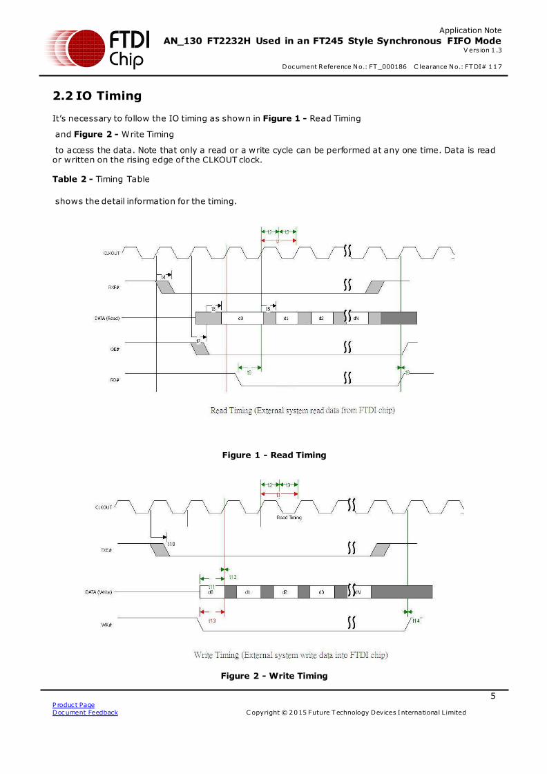
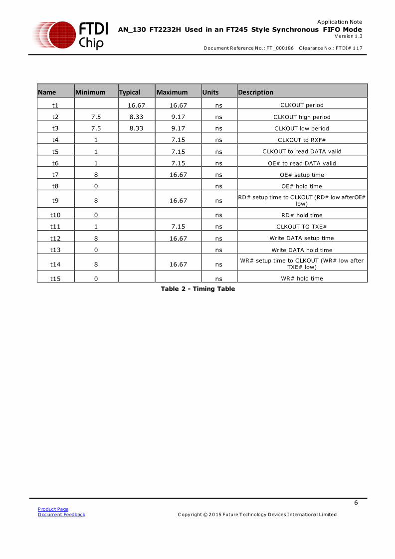
2.2 IO Timing
It’s necessary to follow the IO timing as shown in Figure 1 - Read Timing
and Figure 2 - Write Timing
to access the data. Note that only a read or a write cycle can be performed at any one time. Data is read or written on the rising edge of the CLKOUT clock.
Table 2 - Timing Table
shows the detail information for the timing.
Figure 1 - Read Timing
Figure 2 - Write Timing
6 P roduc t Page
Document Feedback C opyright © 2015 Future Technology Devices International Limited
Application Note
AN_130 FT2232H Used in an FT245 Style Synchronous FIFO Mode V ers ion 1 .3
Document Reference No.: FT_000186 C learance No.: FTDI# 117
Name Minimum Typical Maximum Units Description
t1
16.67 16.67 ns CLKOUT period
t2 7.5 8.33 9.17 ns CLKOUT high period
t3 7.5 8.33 9.17 ns CLKOUT low period
t4 1
7.15 ns CLKOUT to RXF#
t5 1
7.15 ns CLKOUT to read DATA valid
t6 1
7.15 ns OE# to read DATA valid
t7 8
16.67 ns OE# setup time
t8 0
ns OE# hold time
t9 8
16.67 ns RD# setup time to CLKOUT (RD# low afterOE#
low)
t10 0
ns RD# hold time
t11 1
7.15 ns CLKOUT TO TXE#
t12 8
16.67 ns Write DATA setup time
t13 0
ns Write DATA hold time
t14 8 16.67 ns WR# setup time to CLKOUT (WR# low after
TXE# low)
t15 0 ns WR# hold time
Table 2 - Timing Table
7 P roduc t Page
Document Feedback C opyright © 2015 Future Technology Devices International Limited
Application Note
AN_130 FT2232H Used in an FT245 Style Synchronous FIFO Mode V ers ion 1 .3
Document Reference No.: FT_000186 C learance No.: FTDI# 117
3 Software Configuration
With the FT2232H device, it is necessary to install the FTDI D2XX driver on the PC. Please visit the FTDI
Drivers page to download and install the necessary driver which matches the PC.
The table below is taken from the FT2232H datasheet. It indicates that it is necessary to set the FT245 mode by configuring the EEPROM to 245 FIFO modes before developing a software application to access
data under FT245 style Sync FIFO mode. Configuring the EEPROM is illustrated in chapter 3.1 Developing software application is illustrated in chapter4.
SYNC 245 FIFO
EEPROM configured YES
Application Software
configured YES
Table 3 - Configuration using EEPROM and Application Software
8 P roduc t Page
Document Feedback C opyright © 2015 Future Technology Devices International Limited
Application Note
AN_130 FT2232H Used in an FT245 Style Synchronous FIFO Mode V ers ion 1 .3
Document Reference No.: FT_000186 C learance No.: FTDI# 117
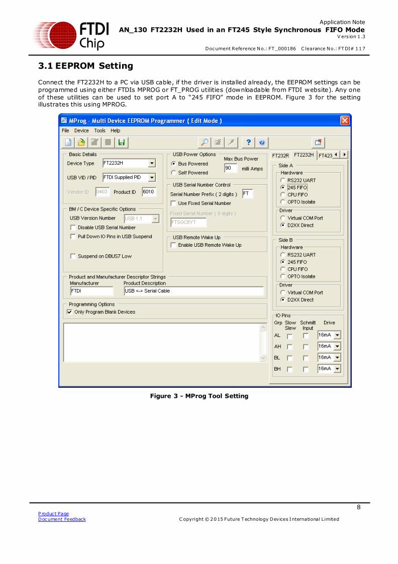
3.1 EEPROM Setting
Connect the FT2232H to a PC via USB cable, if the driver is installed already, the EEPROM settings can be
programmed using either FTDIs MPROG or FT_PROG utilities (downloadable from FTDI website). Any one
of these utilities can be used to set port A to “245 FIFO” mode in EEPROM. Figure 3 for the setting illustrates this using MPROG.
Figure 3 - MProg Tool Setting
9 P roduc t Page
Document Feedback C opyright © 2015 Future Technology Devices International Limited
Application Note
AN_130 FT2232H Used in an FT245 Style Synchronous FIFO Mode V ers ion 1 .3
Document Reference No.: FT_000186 C learance No.: FTDI# 117
4 Application Development
As shown in Table 3 - Configuration using EEPROM and Application Software, it is necessary to develop
an application to access data under FT245 style Sync FIFO mode. In following section describes how to do
this.
In the application code, it is firstly necessary to open Port A of the FT2232H.
Next send command FT_SetBitMode(Mask, 0x40) to the FTDI driver to switch the FT2232H to FT245 Synchronous FIFO mode (this mode uses the RX & TX buffer of port B, so port B cannot be used for any
other purpose in this mode).
Then we can send command FT_SetLatencyTimer(ftHandle, latencytime) to the FTDI driver to configure
latency time, which is the receive buffer timeout that is used to flush remaining data from the receive buffer. If you don’t call this command, the default setting is 16ms; it can be set at 1 ms intervals
between 2ms and 255 ms.
The command FT_SetUSBParameters() can then be used to set the USB buffer size for the required data
transfer. The buffer sizes must be set to a multiple of 64 bytes between 64 bytes and 64k bytes . The default size is 4KB. It is recommended changing this to 64KB.
Next the command, FT_SetFlowControl(), should to be called and parameter usFlowControl used to set
FT_FLOW_RTS_CTS. This is configures the device driver to avoid data loss.
When the FT2232H has been set to FT245 Synchronous FIFO mode, the CLKOUT pin will output 60MHz a
clock. Observing this with an oscilloscope is a good check to make sure the interface has entered FT245 Synchronous FIFO mode. If the waveform edges do not appear sharp enough, then the drive strength of
the IO can be increased by altering the EEPROM values using MPROG or FT_PROG.
Although the RX and TX buffers are 4KB, they only use 2x 512 bytes for each buffer under FT245
Synchronous FIFO mode (maximum USB2.0 packet size under BULK mode is 512 bytes). The two buffers continually swap between each other to increase the performance.
To use the software commands, it is necessary to download the ftd2xx.dll, ftd2xx.lib, ftd2xx.h from the FTDI CDM driver. Details on how to use the software commands are available in the D2XX Programmers
Guide.
10 P roduc t Page
Document Feedback C opyright © 2015 Future Technology Devices International Limited
Application Note
AN_130 FT2232H Used in an FT245 Style Synchronous FIFO Mode V ers ion 1 .3
Document Reference No.: FT_000186 C learance No.: FTDI# 117
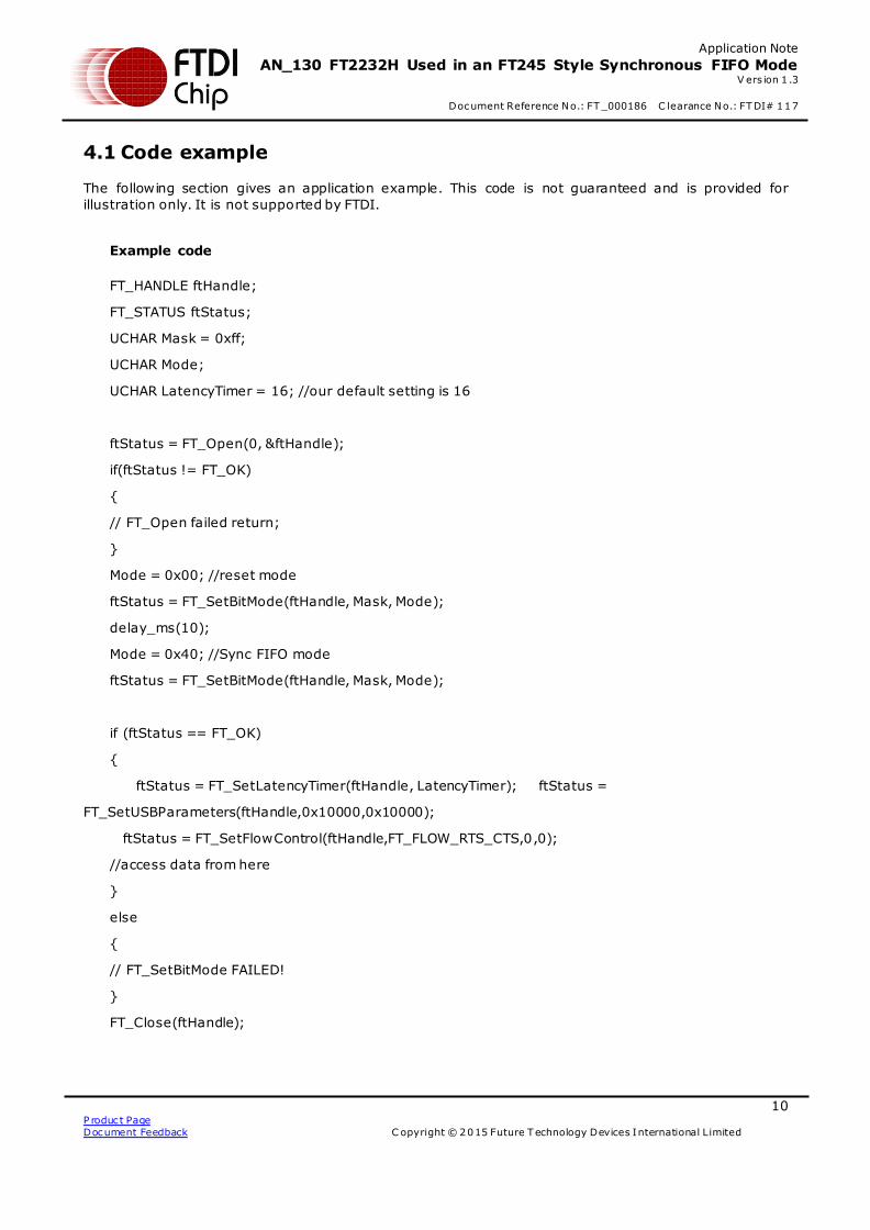
4.1 Code example
The following section gives an application example. This code is not guaranteed and is provided for
illustration only. It is not supported by FTDI.
Example code
FT_HANDLE ftHandle;
FT_STATUS ftStatus;
UCHAR Mask = 0xff;
UCHAR Mode;
UCHAR LatencyTimer = 16; //our default setting is 16
ftStatus = FT_Open(0, &ftHandle);
if(ftStatus != FT_OK)
{
// FT_Open failed return;
}
Mode = 0x00; //reset mode
ftStatus = FT_SetBitMode(ftHandle, Mask, Mode);
delay_ms(10);
Mode = 0x40; //Sync FIFO mode
ftStatus = FT_SetBitMode(ftHandle, Mask, Mode);
if (ftStatus == FT_OK)
{
ftStatus = FT_SetLatencyTimer(ftHandle, LatencyTimer); ftStatus =
FT_SetUSBParameters(ftHandle,0x10000,0x10000);
ftStatus = FT_SetFlowControl(ftHandle,FT_FLOW_RTS_CTS,0,0);
//access data from here
}
else
{
// FT_SetBitMode FAILED!
}
FT_Close(ftHandle);
11 P roduc t Page
Document Feedback C opyright © 2015 Future Technology Devices International Limited
Application Note
AN_130 FT2232H Used in an FT245 Style Synchronous FIFO Mode V ers ion 1 .3
Document Reference No.: FT_000186 C learance No.: FTDI# 117
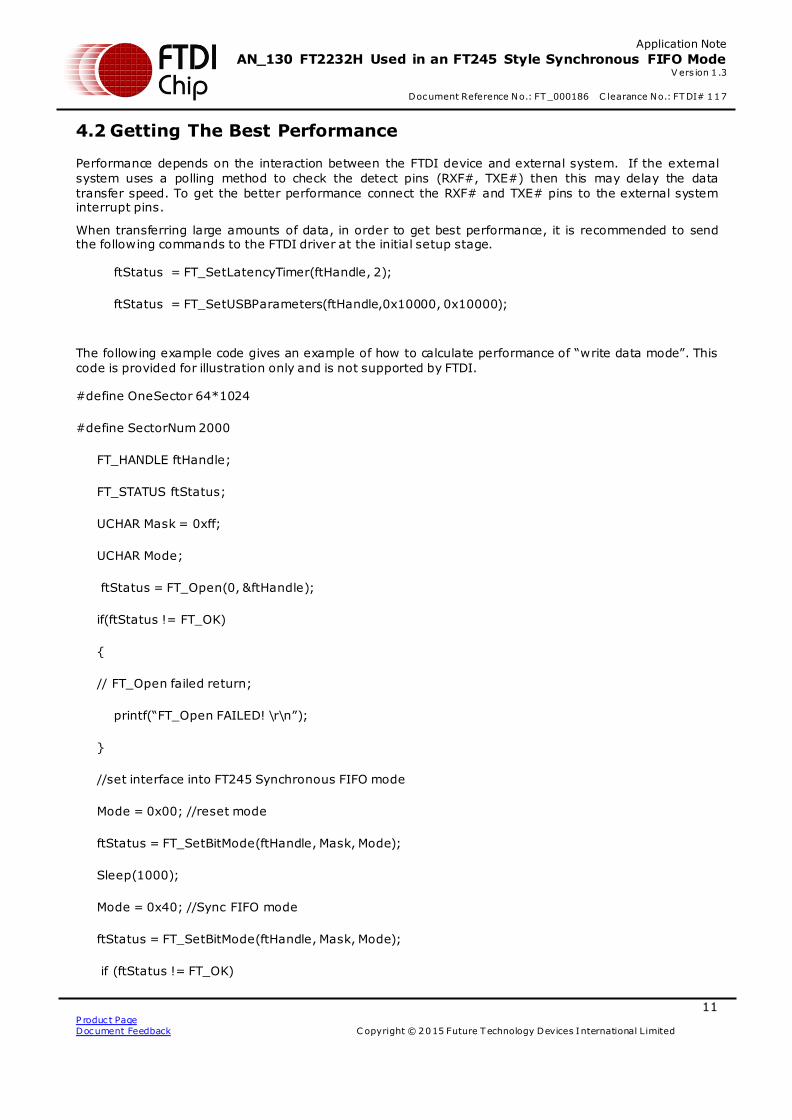
4.2 Getting The Best Performance
Performance depends on the interaction between the FTDI device and external system. If the external
system uses a polling method to check the detect pins (RXF#, TXE#) then this may delay the data
transfer speed. To get the better performance connect the RXF# and TXE# pins to the external system interrupt pins.
When transferring large amounts of data, in order to get best performance, it is recommended to send the following commands to the FTDI driver at the initial setup stage.
ftStatus = FT_SetLatencyTimer(ftHandle, 2);
ftStatus = FT_SetUSBParameters(ftHandle,0x10000, 0x10000);
The following example code gives an example of how to calculate performance of “write data mode”. This
code is provided for illustration only and is not supported by FTDI.
#define OneSector 64*1024
#define SectorNum 2000
FT_HANDLE ftHandle;
FT_STATUS ftStatus;
UCHAR Mask = 0xff;
UCHAR Mode;
ftStatus = FT_Open(0, &ftHandle);
if(ftStatus != FT_OK)
{
// FT_Open failed return;
printf(“FT_Open FAILED! \r\n”);
}
//set interface into FT245 Synchronous FIFO mode
Mode = 0x00; //reset mode
ftStatus = FT_SetBitMode(ftHandle, Mask, Mode);
Sleep(1000);
Mode = 0x40; //Sync FIFO mode
ftStatus = FT_SetBitMode(ftHandle, Mask, Mode);
if (ftStatus != FT_OK)
12 P roduc t Page
Document Feedback C opyright © 2015 Future Technology Devices International Limited
Application Note
AN_130 FT2232H Used in an FT245 Style Synchronous FIFO Mode V ers ion 1 .3
Document Reference No.: FT_000186 C learance No.: FTDI# 117
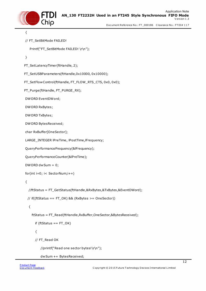
{
// FT_SetBitMode FAILED!
Printf(“FT_SetBitMode FAILED! \r\n”);
}
FT_SetLatencyTimer(ftHandle, 2);
FT_SetUSBParameters(ftHandle,0x10000, 0x10000);
FT_SetFlowControl(ftHandle, FT_FLOW_RTS_CTS, 0x0, 0x0);
FT_Purge(ftHandle, FT_PURGE_RX);
DWORD EventDWord;
DWORD RxBytes;
DWORD TxBytes;
DWORD BytesReceived;
char RxBuffer[OneSector];
LARGE_INTEGER lPreTime, lPostTime,lFrequency;
QueryPerformanceFrequency(&lFrequency);
QueryPerformanceCounter(&lPreTime);
DWORD dwSum = 0;
for(int i=0; i< SectorNum;i++)
{
//ftStatus = FT_GetStatus(ftHandle,&RxBytes,&TxBytes,&EventDWord);
// if((ftStatus == FT_OK) && (RxBytes >= OneSector))
{
ftStatus = FT_Read(ftHandle,RxBuffer,OneSector,&BytesReceived);
if (ftStatus == FT_OK)
{
// FT_Read OK
//printf(“Read one sector bytes!\r\n”);
dwSum += BytesReceived;
13 P roduc t Page
Document Feedback C opyright © 2015 Future Technology Devices International Limited
Application Note
AN_130 FT2232H Used in an FT245 Style Synchronous FIFO Mode V ers ion 1 .3
Document Reference No.: FT_000186 C learance No.: FTDI# 117
}
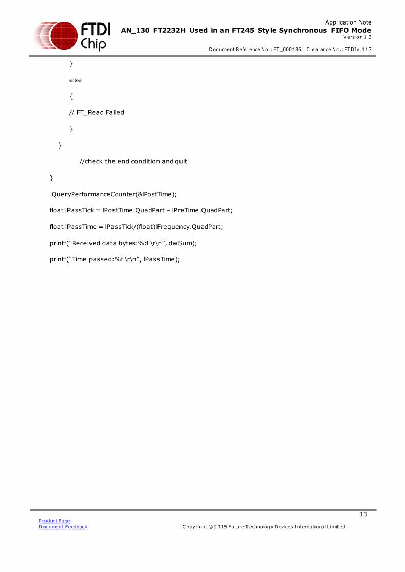
else
{
// FT_Read Failed
}
}
//check the end condition and quit
}
QueryPerformanceCounter(&lPostTime);
float lPassTick = lPostTime.QuadPart – lPreTime.QuadPart;
float lPassTime = lPassTick/(float)lFrequency.QuadPart;
printf(“Received data bytes:%d \r\n”, dwSum);
printf(“Time passed:%f \r\n”, lPassTime);
14 P roduc t Page
Document Feedback C opyright © 2015 Future Technology Devices International Limited
Application Note
AN_130 FT2232H Used in an FT245 Style Synchronous FIFO Mode V ers ion 1 .3
Document Reference No.: FT_000186 C learance No.: FTDI# 117
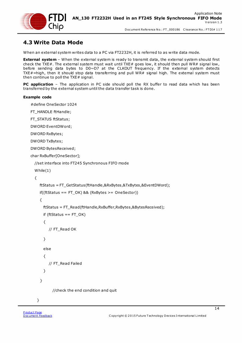
4.3 Write Data Mode
When an external system writes data to a PC via FT2232H, it is referred to as write data mode.
External system – When the external system is ready to transmit data, the external system should first
check the TXE#. The external system must wait until TXE# goes low, it should then pull WR# signal low, before sending data bytes to D0~D7 at the CLKOUT frequency. If the external system detects
TXE#=high, then it should stop data transferring and pull WR# signal high. The external system must then continue to poll the TXE# signal.
PC application – The application in PC side should poll the RX buffer to read data which has been transferred by the external system until the data transfer task is done.
Example code
#define OneSector 1024
FT_HANDLE ftHandle;
FT_STATUS ftStatus;
DWORD EventDWord;
DWORD RxBytes;
DWORD TxBytes;
DWORD BytesReceived;
char RxBuffer[OneSector];
//set interface into FT245 Synchronous FIFO mode
While(1)
{
ftStatus = FT_GetStatus(ftHandle,&RxBytes,&TxBytes,&EventDWord);
if((ftStatus == FT_OK) && (RxBytes >= OneSector))
{
ftStatus = FT_Read(ftHandle,RxBuffer,RxBytes,&BytesReceived);
if (ftStatus == FT_OK)
{
// FT_Read OK
}
else
{
// FT_Read Failed
}
}
//check the end condition and quit
}
15 P roduc t Page
Document Feedback C opyright © 2015 Future Technology Devices International Limited
Application Note
AN_130 FT2232H Used in an FT245 Style Synchronous FIFO Mode V ers ion 1 .3
Document Reference No.: FT_000186 C learance No.: FTDI# 117
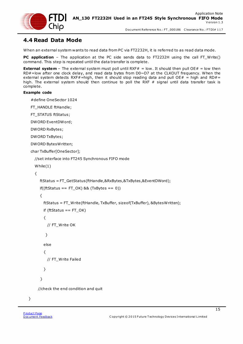
4.4 Read Data Mode
When an external system wants to read data from PC via FT2232H, it is referred to as read data mode.
PC application – The application at the PC side sends data to FT2232H using the call FT_Write()
command. This step is repeated until the data transfer is complete.
External system – The external system must poll until RXF# = low. It should then pull OE# = low then
RD#=low after one clock delay, and read data bytes from D0~D7 at the CLKOUT frequency. When the external system detects RXF#=high, then it should stop reading data and pull OE# = high and RD#=
high. The external system should then continue to poll the RXF # signal until data transfer task is complete.
Example code
#define OneSector 1024
FT_HANDLE ftHandle;
FT_STATUS ftStatus;
DWORD EventDWord;
DWORD RxBytes;
DWORD TxBytes;
DWORD BytesWritten;
char TxBuffer[OneSector];
//set interface into FT245 Synchronous FIFO mode
While(1)
{
ftStatus = FT_GetStatus(ftHandle,&RxBytes,&TxBytes,&EventDWord);
if((ftStatus == FT_OK) && (TxBytes == 0))
{
ftStatus = FT_Write(ftHandle, TxBuffer, sizeof(TxBuffer), &BytesWritten);
if (ftStatus == FT_OK)
{
// FT_Write OK
}
else
{
// FT_Write Failed
}
}
//check the end condition and quit
}
16 P roduc t Page
Document Feedback C opyright © 2015 Future Technology Devices International Limited
Application Note
AN_130 FT2232H Used in an FT245 Style Synchronous FIFO Mode V ers ion 1 .3
Document Reference No.: FT_000186 C learance No.: FTDI# 117
5 Contact Information
Head Office – Glasgow, UK Branch Office – Tigard, Oregon, USA Future Technology Devices International Limited Unit 1, 2 Seaward Place, Centurion Business Park Glasgow G41 1HH United Kingdom Tel: +44 (0) 141 429 2777
Fax: +44 (0) 141 429 2758
Future Technology Devices International Limited (USA) 7130 SW Fir Loop Tigard, OR 97223-8160 USA Tel: +1 (503) 547 0988
Fax: +1 (503) 547 0987 E-mail (Sales) [email protected] E-Mail (Sales) [email protected] E-mail (Support) [email protected] E-Mail (Support) [email protected] E-mail (General Enquiries) [email protected] E-Mail (General Enquiries) [email protected]
Branch Office – Taipei, Taiwan Branch Office – Shanghai, China Future Technology Devices International Limited (Taiwan) 2F, No. 516, Sec. 1, NeiHu Road Taipei 114 Taiwan , R.O.C. Tel: +886 (0) 2 8791 3570
Fax: +886 (0) 2 8791 3576
Future Technology Devices International Limited (China) Room 1103, No. 666 West Huaihai Road, Shanghai, 200052 China Tel: +86 21 62351596 Fax: +86 21 62351595
E-mail (Sales) [email protected] E-Mail (Sales) [email protected] E-mail (Support) [email protected] E-Mail (Support) [email protected] E-mail (General Enquiries) [email protected] E-Mail (General Enquiries) [email protected]
Web Site
http://ftdichip.com
Distributor and Sales Representatives
Please visit the Sales Network page of the FTDI Web site for the contact details of our distributor(s) and
sales representative(s) in your country.
Vinculum is part of Future Technology Devices International Ltd. Neither the whole nor any part of the information contained in, or the
produc t described in this manual, may be adapted or reproduced in any material or electronic form without the prior written consent of
the copyright holder. This produc t and its documentation are supplied on an as-is bas is and no warranty as to their suitability for any
particular purpose is either made or implied. Future Technology Devices International Ltd will not accept any claim for damages
howsoever aris ing as a result of use or failure of this produc t. Your statutory rights are not affected. This product or any variant of it is
not intended for use in any medical appliance, device or sys tem in which the failure of the product might reasonably be expec ted to
result in personal injury. This document provides preliminary information that may be subject to change without notice. No fr eedom to
use patents or other intellectual property rights is implied by the publication of this document. Future Technology Devices International
Ltd, Unit 1 , 2 Seaward P lace, C enturion Business P ark, Glasgow G41 1HH United Kingdom. Scotland Registered Number: SC 136640
17 P roduc t Page
Document Feedback C opyright © 2015 Future Technology Devices International Limited
Application Note
AN_130 FT2232H Used in an FT245 Style Synchronous FIFO Mode V ers ion 1 .3
Document Reference No.: FT_000186 C learance No.: FTDI# 117
Appendix A – References
Document References
D2XX Programmers Guide
Acronyms and Abbreviations
Terms Description
EEPROM Electrically Erasable Programmable Read-Only Memory
FIFO First-In First-Out
PC Personal Computer
USB Universal Serial Bus
18 P roduc t Page
Document Feedback C opyright © 2015 Future Technology Devices International Limited
Application Note
AN_130 FT2232H Used in an FT245 Style Synchronous FIFO Mode V ers ion 1 .3
Document Reference No.: FT_000186 C learance No.: FTDI# 117
Appendix B – List of Tables & Figures
List of Tables
Table 1 - Channel A FT245 Style Synchronous FIFO Configured Pin Descriptions ..................................... 4
Table 2 - Timing Table............................................................................................................................ 6
Table 3 - Configuration using EEPROM and Application Software ............................................................. 7
List of Figures
Figure 1 - Read Timing ........................................................................................................................... 5
Figure 2 - Write Timing........................................................................................................................... 5
Figure 3 - MProg Tool Setting ................................................................................................................. 8
19 P roduc t Page
Document Feedback C opyright © 2015 Future Technology Devices International Limited
Application Note
AN_130 FT2232H Used in an FT245 Style Synchronous FIFO Mode V ers ion 1 .3
Document Reference No.: FT_000186 C learance No.: FTDI# 117
Appendix C– Revision History
Document Title: AN_130 FT2232H Used in an FT245 Style Synchronous FIFO Mode
Document Reference No.: FT_000186
Clearance No.: FTDI# 117
Product Page: http://www.ftdichip.com/FTProducts.htm
Document Feedback: Send Feedback
Revision Changes Date
1.0 Initial release 2009-10-23
1.1 Added Chapter 4.2 Getting the Best Performance 2009-10-30
1.2 Edited Figure 3.1 MProg tool setting 2010-03-05
1.3 Updated Table 2 – Timing Table 2015-11-17