FSBB30CH60C - RS Components...
15
FSBB30CH60C Motion SPM® 3 Series January 2014 ©2008 Fairchild Semiconductor Corporation 1 www.fairchildsemi.com FSBB30CH60C Rev. C3 FSBB30CH60C Motion SPM ® 3 Series Features • UL Certified No. E209204 (UL1557) • 600 V - 30 A 3-Phase IGBT Inverter with Integral Gate Drivers and Protection • Low-Loss, Short-Circuit Rated IGBTs • Very Low Thermal Resistance Using AlN DBC Sub- strate • Built-In Bootstrap Diodes and Dedicated Vs Pins Sim- plify PCB Layout • Separate Open-Emitter Pins from Low-Side IGBTs for Three-Phase Current Sensing • Single-Grounded Power Supply • Isolation Rating: 2500 V rms / min. Applications • Motion Control - Home Appliance / Industrial Motor Related Resources • AN-9044 - Motion SPM® 3 Series Users Guide General Description FSBB30CH60C is an advanced Motion SPM ® 3 module providing a fully-featured, high-performance inverter out- put stage for AC Induction, BLDC, and PMSM motors. These modules integrate optimized gate drive of the built-in IGBTs to minimize EMI and losses, while also providing multiple on-module protection features includ- ing under-voltage lockouts, over-current shutdown, and fault reporting. The built-in, high-speed HVIC requires only a single supply voltage and translates the incoming logic-level gate inputs to the high-voltage, high-current drive signals required to properly drive the module's internal IGBTs. Separate negative IGBT terminals are available for each phase to support the widest variety of control algorithms. Package Marking and Ordering Information Figure 1. Package Overview Device Device Marking Package Packing Type Quantity FSBB30CH60C FSBB30CH60C SPMEC-027 Rail 10
Transcript of FSBB30CH60C - RS Components...

FS
BB
30CH
60C M
otio
n S
PM
® 3 S
eries
January 2014
©2008 Fairchild Semiconductor Corporation 1 www.fairchildsemi.comFSBB30CH60C Rev. C3
FSBB30CH60CMotion SPM® 3 Series
Features• UL Certified No. E209204 (UL1557)
• 600 V - 30 A 3-Phase IGBT Inverter with Integral GateDrivers and Protection
• Low-Loss, Short-Circuit Rated IGBTs
• Very Low Thermal Resistance Using AlN DBC Sub-strate
• Built-In Bootstrap Diodes and Dedicated Vs Pins Sim-plify PCB Layout
• Separate Open-Emitter Pins from Low-Side IGBTs forThree-Phase Current Sensing
• Single-Grounded Power Supply
• Isolation Rating: 2500 Vrms / min.
Applications• Motion Control - Home Appliance / Industrial Motor
Related Resources• AN-9044 - Motion SPM® 3 Series Users Guide
General DescriptionFSBB30CH60C is an advanced Motion SPM® 3 moduleproviding a fully-featured, high-performance inverter out-put stage for AC Induction, BLDC, and PMSM motors.These modules integrate optimized gate drive ofthe built-in IGBTs to minimize EMI and losses, while alsoproviding multiple on-module protection features includ-ing under-voltage lockouts, over-current shutdown, andfault reporting. The built-in, high-speed HVIC requiresonly a single supply voltage and translates the incominglogic-level gate inputs to the high-voltage, high-currentdrive signals required to properly drive the module'sinternal IGBTs. Separate negative IGBT terminals areavailable for each phase to support the widest variety ofcontrol algorithms.
Package Marking and Ordering Information
Figure 1. Package Overview
Device Device Marking Package Packing Type Quantity
FSBB30CH60C FSBB30CH60C SPMEC-027 Rail 10

FS
BB
30CH
60C M
otio
n S
PM
® 3 S
eries
©2008 Fairchild Semiconductor Corporation 2 www.fairchildsemi.comFSBB30CH60C Rev. C3
Integrated Power Functions• 600 V - 30 A IGBT inverter for three-phase DC / AC power conversion (please refer to Figure 3)
Integrated Drive, Protection, and System Control Functions• For inverter high-side IGBTs: gate drive circuit, high-voltage isolated high-speed level shifting
control circuit Under-Voltage Lock-Out Protection (UVLO) Note: Available bootstrap circuit example is given in Figures 12 and 13.
• For inverter low-side IGBTs: gate drive circuit, Short-Circuit Protection (SCP) control supply circuit Under-Voltage Lock-Out Protection (UVLO)
• Fault signaling: corresponding to UVLO (low-side supply) and SC faults
• Input interface: active-HIGH interface, works with 3.3 / 5 V logic, Schmitt-trigger input
Pin Configuration
Figure 2. Top View

FS
BB
30CH
60C M
otio
n S
PM
® 3 S
eries
©2008 Fairchild Semiconductor Corporation 3 www.fairchildsemi.comFSBB30CH60C Rev. C3
Pin Descriptions
Pin Number Pin Name Pin Description
1 VCC(L) Low-Side Common Bias Voltage for IC and IGBTs Driving
2 COM Common Supply Ground
3 IN(UL) Signal Input for Low-Side U-Phase
4 IN(VL) Signal Input for Low-Side V-Phase
5 IN(WL) Signal Input for Low-Side W-Phase
6 VFO Fault Output
7 CFOD Capacitor for Fault Output Duration Selection
8 CSC Capacitor (Low-Pass Filter) for Short-Circuit Current Detection Input
9 IN(UH) Signal Input for High-Side U-Phase
10 VCC(H) High-Side Common Bias Voltage for IC and IGBTs Driving
11 VB(U) High-Side Bias Voltage for U-Phase IGBT Driving
12 VS(U) High-Side Bias Voltage Ground for U-Phase IGBT Driving
13 IN(VH) Signal Input for High-Side V-Phase
14 VCC(H) High-Side Common Bias Voltage for IC and IGBTs Driving
15 VB(V) High-Side Bias Voltage for V-Phase IGBT Driving
16 VS(V) High-Side Bias Voltage Ground for V Phase IGBT Driving
17 IN(WH) Signal Input for High-Side W-Phase
18 VCC(H) High-Side Common Bias Voltage for IC and IGBTs Driving
19 VB(W) High-Side Bias Voltage for W-Phase IGBT Driving
20 VS(W) High-Side Bias Voltage Ground for W-Phase IGBT Driving
21 NU Negative DC-Link Input for U-Phase
22 NV Negative DC-Link Input for V-Phase
23 NW Negative DC-Link Input for W-Phase
24 U Output for U-Phase
25 V Output for V-Phase
26 W Output for W-Phase
27 P Positive DC-Link Input
FS
BB
30CH
60C M
otio
n S
PM
® 3 S
eries
©2008 Fairchild Semiconductor Corporation 4 www.fairchildsemi.comFSBB30CH60C Rev. C3
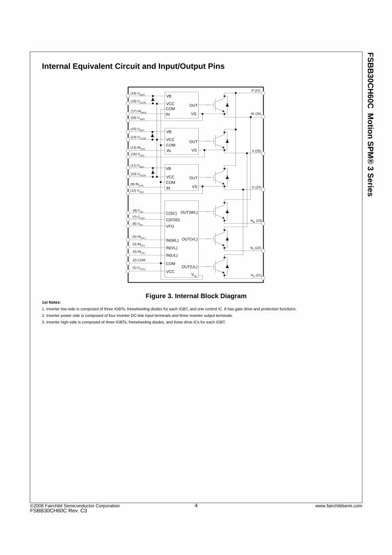
Internal Equivalent Circuit and Input/Output Pins
Figure 3. Internal Block Diagram1st Notes:
1. Inverter low-side is composed of three IGBTs, freewheeling diodes for each IGBT, and one control IC. It has gate drive and protection functions.
2. Inverter power side is composed of four inverter DC-link input terminals and three inverter output terminals.
3. Inverter high-side is composed of three IGBTs, freewheeling diodes, and three drive ICs for each IGBT.
COM
VCC
IN(UL)
IN(VL)
IN(WL)
VFO
C(FOD)
C(SC)
OUT(UL)
OUT(VL)
OUT(WL)
NU (21)
NV (22)
NW (23)
U (24)
V (25)
W (26)
P (27)
(20) VS(W)
(19) VB(W)
(16) VS(V)
(15) VB(V)
(8) CSC
(7) CFOD
(6) VFO
(5) IN(WL)
(4) IN(VL)
(3) IN(UL)
(2) COM
(1) VCC(L)
VCC
VB
OUTCOM
VSIN
VB
VS
OUT
IN
COMVCC
VCC
VB
OUTCOM
VSIN
(18) VCC(H)
(17) IN(WH)
(14) VCC(H)
(13) IN(VH)
(12) VS(U)
(11) VB(U)
(10) VCC(H)
(9) IN(UH)
VSL

FS
BB
30CH
60C M
otio
n S
PM
® 3 S
eries
©2008 Fairchild Semiconductor Corporation 5 www.fairchildsemi.comFSBB30CH60C Rev. C3
Absolute Maximum Ratings (TJ = 25°C, unless otherwise specified.)
Inverter Part
2nd Notes:
1. The maximum junction temperature rating of the power chips integrated within the Motion SPM® 3 product is 150C (at TC 125C).
Control Part
Bootstrap Diode Part
Total System
Thermal Resistance
2nd Notes:
2. For the measurement point of case temperature (TC), please refer to Figure 2.
Symbol Parameter Conditions Rating Unit
VPN Supply Voltage Applied between P - NU, NV, NW 450 V
VPN(Surge) Supply Voltage (Surge) Applied between P - NU, NV, NW 500 V
VCES Collector - Emitter Voltage 600 V
± IC Each IGBT Collector Current TC = 25°C, TJ 150°C 30 A
± ICP Each IGBT Collector Current (Peak) TC = 25°C, TJ 150°C, Under 1 ms PulseWidth
60 A
PC Collector Dissipation TC = 25°C per Chip 106 W
TJ Operating Junction Temperature (2nd Note 1) -40 ~ 150 °C
Symbol Parameter Conditions Rating Unit
VCC Control Supply Voltage Applied between VCC(H), VCC(L) - COM 20 V
VBS High-Side Control Bias Voltage Applied between VB(U) - VS(U), VB(V) - VS(V),VB(W) - VS(W)
20 V
VIN Input Signal Voltage Applied between IN(UH), IN(VH), IN(WH),IN(UL), IN(VL), IN(WL) - COM
-0.3 ~ VCC + 0.3 V
VFO Fault Output Supply Voltage Applied between VFO - COM -0.3 ~ VCC + 0.3 V
IFO Fault Output Current Sink Current at VFO pin 5 mA
VSC Current-Sensing Input Voltage Applied between CSC - COM -0.3 ~ VCC + 0.3 V
Symbol Parameter Conditions Rating Unit
VRRM Maximum Repetitive Reverse Voltage 600 V
IF Forward Current TC = 25°C, TJ 150°C 0.5 A
IFP Forward Current (Peak) TC = 25°C, TJ 150°C Under 1 ms PulseWidth
2.0 A
TJ Operating Junction Temperature -40 ~ 150 °C
Symbol Parameter Conditions Rating Unit
VPN(PROT) Self-Protection Supply Voltage Limit(Short-Circuit Protection Capability)
VCC = VBS = 13.5 ~ 16.5 VTJ = 150°C, Non-Repetitive, < 2 s
400 V
TC Module Case Operation Temperature -40CTJ 150C, See Figure 2 -40 ~ 125 °C
TSTG Storage Temperature -40 ~ 125 °C
VISO Isolation Voltage 60 Hz, Sinusoidal, AC 1 Minute, ConnectPins to Heat Sink Plate
2500 Vrms
Symbol Parameter Conditions Min. Typ. Max. Unit
Rth(j-c)Q Junction to Case Thermal Resistance Inverter IGBT Part (per 1 / 6 module) - - 1.17 °C / W
Rth(j-c)F Inverter FWDi Part (per 1 / 6 module) - - 1.87 °C / W

FS
BB
30CH
60C M
otio
n S
PM
® 3 S
eries
©2008 Fairchild Semiconductor Corporation 6 www.fairchildsemi.comFSBB30CH60C Rev. C3
Electrical Characteristics (TJ = 25°C, unless otherwise specified.)
Inverter Part
2nd Notes:
3. tON and tOFF include the propagation delay of the internal drive IC. tC(ON) and tC(OFF) are the switching time of IGBT itself under the given gate driving condition internally. Forthe detailed information, please see Figure 4.
Control Part
2nd Notes:
4. Short-circuit protection is functioning only at the low-sides.
5. The fault-out pulse width tFOD depends on the capacitance value of CFOD according to the following approximate equation: CFOD = 18.3 x 10⁻⁶ x tFOD [F]
Symbol Parameter Conditions Min. Typ. Max. Unit
VCE(SAT) Collector - Emitter SaturationVoltage
VCC = VBS = 15 VVIN = 5 V
IC = 20 A, TJ = 25°C - - 2.0 V
VF FWDi Forward Voltage VIN = 0 V IF = 20 A, TJ = 25°C - - 2.1 V
HS tON Switching Times VPN = 300 V, VCC = VBS = 15 VIC = 30 AVIN = 0 V 5 V, Inductive Load(2nd Note 3)
- 0.75 - s
tC(ON) - 0.2 - s
tOFF - 0.4 - s
tC(OFF) - 0.1 - s
trr - 0.1 - s
LS tON VPN = 300 V, VCC = VBS = 15 VIC = 30 AVIN = 0 V 5 V, Inductive Load(2nd Note 3)
- 0.55 - s
tC(ON) - 0.35 - s
tOFF - 0.4 - s
tC(OFF) - 0.1 - s
trr - 0.1 - s
ICES Collector - Emitter LeakageCurrent
VCE = VCES - - 1 mA
Symbol Parameter Conditions Min. Typ. Max. Unit
IQCCL Quiescent VCC SupplyCurrent
VCC = 15 VIN(UL, VL, WL) = 0 V
VCC(L) - COM - - 23 mA
IQCCH VCC = 15 VIN(UH, VH, WH) = 0 V
VCC(H) - COM - - 600 A
IQBS Quiescent VBS SupplyCurrent
VBS = 15 VIN(UH, VH, WH) = 0 V
VB(U) - VS(U), VB(V) - VS(V), VB(W) - VS(W)
- - 500 A
VFOH Fault Output Voltage VSC = 0 V, VFO Circuit: 4.7 k to 5 V Pull-up 4.5 - - V
VFOL VSC = 1 V, VFO Circuit: 4.7 k to 5 V Pull-up - - 0.8 V
VSC(ref) Short-Circuit Current Trip Level
VCC = 15 V (2nd Note 4) 0.45 0.50 0.55 V
TSD Over-Temperature Protection
Temperature at LVIC - 160 - °C
TSD Over-Temperature Protection Hysterisis
Temperature at LVIC - 5 - °C
UVCCD Supply Circuit Under-Voltage Protection
Detection Level 10.7 11.9 13.0 V
UVCCR Reset Level 11.2 12.4 13.4 V
UVBSD Detection Level 10 11 12 V
UVBSR Reset Level 10.5 11.5 12.5 V
tFOD Fault-Out Pulse Width CFOD = 33 nF (2nd Note 5) 1.0 1.8 - ms
VIN(ON) ON Threshold Voltage Applied between IN(UH), IN(VH), IN(WH), IN(UL),IN(VL), IN(WL) - COM
2.8 - - V
VIN(OFF) OFF Threshold Voltage - - 0.8 V
FS
BB
30CH
60C M
otio
n S
PM
® 3 S
eries
©2008 Fairchild Semiconductor Corporation 7 www.fairchildsemi.comFSBB30CH60C Rev. C3
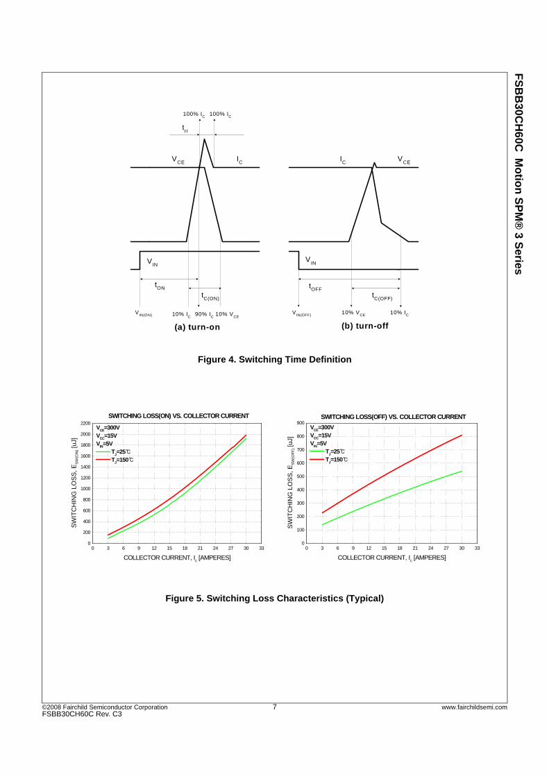
Figure 4. Switching Time Definition
Figure 5. Switching Loss Characteristics (Typical)
VCE IC
VIN
tON
tC(ON)
VIN(ON) 10% IC
10% VCE
90% IC
100% IC
trr
100% IC
0
VCEIC
VIN
tOFFtC(OFF)
VIN(OFF) 10% VCE 10% IC
(a) turn-on (b) turn-off
0 3 6 9 12 15 18 21 24 27 30 330
200
400
600
800
1000
1200
1400
1600
1800
2000
2200
SWITCHING LOSS(ON) VS. COLLECTOR CURRENT
VCE
=300VVCC=15VV
IN=5V
TJ=25
TJ=150
SW
ITC
HIN
G L
OS
S, E
SW
(ON
) [uJ
]
COLLECTOR CURRENT, Ic [AMPERES]
0 3 6 9 12 15 18 21 24 27 30 330
100
200
300
400
500
600
700
800
900SWITCHING LOSS(OFF) VS. COLLECTOR CURRENT
VCE
=300VV
CC=15V
VIN=5V
TJ=25
TJ=150
SW
ITC
HIN
G L
OS
S,
ES
W(O
FF
) [uJ
]
COLLECTOR CURRENT, Ic [AMPERES]

FS
BB
30CH
60C M
otio
n S
PM
® 3 S
eries
©2008 Fairchild Semiconductor Corporation 8 www.fairchildsemi.comFSBB30CH60C Rev. C3
Bootstrap Diode Part
Figure 6. Built-in Bootstrap Diode Characteristics2nd Notes:
6. Built-in bootstrap diode includes around 15 Ω resistance characteristic.
Recommended Operating Conditions
Symbol Parameter Conditions Min. Typ. Max. Unit
VF Forward Voltage IF = 0.1 A, TC = 25°C - 2.5 - V
trr Reverse-Recovery Time IF = 0.1 A, TC = 25°C - 80 - ns
Symbol Parameter Conditions Min. Typ. Max. Unit
VPN Supply Voltage Applied between P - NU, NV, NW - 300 400 V
VCC Control Supply Voltage Applied between VCC(H), VCC(L) - COM 13.5 15.0 16.5 V
VBS High-Side Bias Voltage Applied between VB(U) - VS(U), VB(V) - VS(V),VB(W) - VS(W)
13.0 15.0 18.5 V
dVCC / dt, dVBS / dt
Control Supply Variation -1 - 1 V / s
tdead Blanking Time for PreventingArm-Short
Each Input Signal 2 - - s
fPWM PWM Input Signal -40C TC 125°C, -40C TJ 150°C - - 20 kHz
VSEN Voltage for Current Sensing Applied between NU, NV, NW - COM(Including Surge Voltage)
-4 4 V
0 1 2 3 4 5 6 7 8 9 10 11 12 13 14 150.0
0.1
0.2
0.3
0.4
0.5
0.6
0.7
0.8
0.9
1.0Built-in Bootstrap Diode V
F-I
F Characteristic
TC=25oC
I F [
A]
VF [V]

FS
BB
30CH
60C M
otio
n S
PM
® 3 S
eries
©2008 Fairchild Semiconductor Corporation 9 www.fairchildsemi.comFSBB30CH60C Rev. C3
Mechanical Characteristics and Ratings
Figure 7. Flatness Measurement Position
Parameter Conditions Min. Typ. Max. Unit
Mounting Torque Mounting Screw: M3 Recommended 0.62 N•m 0.51 0.62 0.80 N•m
Device Flatness See Figure 7 0 - +150 m
Weight - 15.00 - g
( + )
( + )
( + )
( + )

FS
BB
30CH
60C M
otio
n S
PM
® 3 S
eries
©2008 Fairchild Semiconductor Corporation 10 www.fairchildsemi.comFSBB30CH60C Rev. C3
Time Charts of Protective Function
a1 : Control supply voltage rises: after the voltage rises UVCCR, the circuits start to operate when next input is applied.
a2 : Normal operation: IGBT ON and carrying current.
a3 : Under-voltage detection (UVCCD).
a4 : IGBT OFF in spite of control input condition.
a5 : Fault output operation starts.
a6 : Under-voltage reset (UVCCR).
a7 : Normal operation: IGBT ON and carrying current.
Figure 8. Under-Voltage Protection (Low-Side)
b1 : Control supply voltage rises: after the voltage reaches UVBSR, the circuits start to operate when next input is applied.
b2 : Normal operation: IGBT ON and carrying current.
b3 : Under-voltage detection (UVBSD).
b4 : IGBT OFF in spite of control input condition, but there is no fault output signal.
b5 : Under-voltage reset (UVBSR).
b6 : Normal operation: IGBT ON and carrying current.
Figure 9. Under-Voltage Protection (High-Side)
Input Signal
Output Current
Fault Output Signal
ControlSupply Voltage
RESET
UVCCR
ProtectionCircuit State
SET RESET
UVCCD
a1
a3
a2a4
a6
a5
a7
Input Signal
Output Current
Fault Output Signal
ControlSupply Voltage
RESET
UVBSR
ProtectionCircuit State
SET RESET
UVBSD
b1
b3
b2b4
b6
b5
High-level (no fault output)

FS
BB
30CH
60C M
otio
n S
PM
® 3 S
eries
©2008 Fairchild Semiconductor Corporation 11 www.fairchildsemi.comFSBB30CH60C Rev. C3
(with the external shunt resistance and CR connection)
c1 : Normal operation: IGBT ON and carrying current.
c2 : Short-circuit current detection (SC trigger).
c3 : Hard IGBT gate interrupt.
c4 : IGBT turns OFF.
c5 : Fault output timer operation starts: the pulse width of the fault output signal is set by the external capacitor CFO.
c6 : Input “LOW”: IGBT OFF state.
c7 : Input “HIGH”: IGBT ON state, but during the active period of fault output, the IGBT doesn’t turn ON.
c8 : IGBT OFF state.
Figure 10. Short-Circuit Protection (Low-Side Operation Only)
Internal IGBTGate - Emitter Voltage
Lower Arms Control Input
Output Current
Sensing Voltageof Shunt Resistance
Fault Output Signal
SC Reference Voltage
CR Circuit Time Constant Delay
SC
Protection Circuit State SET RESET
c6 c7
c3
c2
c1
c8
c4
c5

FS
BB
30CH
60C M
otio
n S
PM
® 3 S
eries
©2008 Fairchild Semiconductor Corporation 12 www.fairchildsemi.comFSBB30CH60C Rev. C3
Figure 11. Recommended MCU I/O Interface Circuit3rd Notes:
1. RC coupling at each input might change depending on the PWM control scheme in the application and the wiring impedance of the application’s printed circuit board. The inputsignal section of the Motion SPM® 3 product integrates a 5 k(typ.) pull-down resistor. Therefore, when using an external filtering resistor, please pay attention to the signalvoltage drop at input terminal.
2. The logic input works with standard CMOS or LSTTL outputs.
Figure 12. Recommended Bootstrap Operation Circuit and Parameters3rd Notes:
3. The ceramic capacitor placed between VCC - COM should be over 1 F and mounted as close to the pins of the Motion SPM 3 product as possible.
MCU
SPM
COM
+5 V
, ,IN(UL) IN(VL) IN(WL)
, ,IN(UH) IN(VH) IN(WH)
VFO
1 nF CPF = 1 nF
RPF = 4.7
100 Ω
100 Ω
1 nF 1 nF
100 Ω
15 V22 µF
0.1 µF
1000 µF 1 µF
One-Leg Diagram of Motion SPM 3 Product
Inverter Output
P
N
These values depend on PWM control algorithm.
Vcc
IN
COM
VB
HO
VS
Vcc
IN
COM
OUT
VSL

FS
BB
30CH
60C M
otio
n S
PM
® 3 S
eries
©2008 Fairchild Semiconductor Corporation 13 www.fairchildsemi.comFSBB30CH60C Rev. C3
Figure 13. Typical Application Circuit4th Notes:
1. To avoid malfunction, the wiring of each input should be as short as possible (less than 2 - 3cm).
2. By virtue of integrating an application-specific type of HVIC inside the Motion SPM® 3 product, direct coupling to MCU terminals without any optocoupler or transformer isola-tion is possible.
3. VFO output is open-collector type. This signal line should be pulled up to the positive side of the 5 V power supply with approximately 4.7 k resistance (please refer toFigure11).
4. CSP15 of around seven times larger than bootstrap capacitor CBS is recommended.
5. VFO output pulse width should be determined by connecting an external capacitor (CFOD) between CFOD (pin 7) and COM (pin 2). (Example: if CFOD = 33 nF, then tFO = 1.8 ms(typ.)) Please refer to the 2nd note 5 for calculation method.
6. Input signal is active-HIGH type. There is a 5 k resistor inside the IC to pull down each input signal line to GND. RC coupling circuits should be used to prevent input signaloscillation. RSCPS time constant should be selected in the range 50 ~ 150 ns. CPS should not be less than 1 nF (recommended RS = 100 Ω , CPS = 1 nF).
7. To prevent errors of the protection function, the wiring around RF and CSC should be as short as possible.
8. In the short-circuit protection circuit, please select the RFCSC time constant in the range 1.5 ~ 2.0 s.
9. Each capacitor should be mounted as close to the pins of the Motion SPM 3 product as possible.
10. To prevent surge destruction, the wiring between the smoothing capacitor and the P & GND pins should be as short as possible. The use of a high-frequency non-inductivecapacitor of around 0.1 ~ 0.22 F between the P & GND pins is recommended.
11. Relays are used in almost every systems of electrical equipment in home appliances. In these cases, there should be sufficient distance between the MCU and the relays.
12. CSPC15 should be over 1 F and mounted as close to the pins of the Motion SPM 3 product as possible.
Fault
+15 V
CBS CBSC
CBS CBSC
CBS CBSC
CSP15 CSPC15
CFOD
+5 V
RPF
CBPF
RS
M
VdcCDCS
Gating UH
Gating VH
Gating WH
Gating WL
Gating VL
Gating UL
CPF
MCU
RFU
RFV
RFW
RSU
RSV
RSW
CFUCFVCFW
W-Phase CurrentV-Phase CurrentU-Phase Current
RF
COM
VCC
IN(UL)
IN(VL)
IN(WL)
VFO
C(FOD)
C(SC)
OUT(UL)
OUT(VL)
OUT(WL)
NU (21)
NV (22)
NW (23)
U (24)
V (25)
W (26)
P (27)
(20) VS(W)
(19) VB(W)
(16) VS(V)
(15) VB(V)
(8) CSC
(7) CFOD
(6) VFO
(5) IN(WL)
(4) IN(VL)
(3) IN(UL)
(2) COM
(1) VCC(L)
VCC
VB
OUTCOM
VSIN
VB
VS
OUT
IN
COM
VCC
VCC
VB
OUTCOM
VSIN
(18) VCC(H)
(17) IN(WH)
(14) VCC(H)
(13) IN(VH)
(12) VS(U)
(11) VB(U)
(10) VCC(H)
(9) IN(UH)
Input Signal for Short-Circuit Protection
CSC
VSL
RS
RS
RS
RS
RS
RS
CPS
CPS
CPS
CPS CPS CPS

FS
BB
30CH
60C M
otio
n S
PM
® 3 S
eries
©2008 Fairchild Semiconductor Corporation 14 www.fairchildsemi.comFSBB30CH60C Rev. C3
Detailed Package Outline Drawings
Package drawings are provided as a service to customers considering Fairchild components. Drawings may change in any manner without notice. Please note the revision and/or data on the drawing and contact a FairchildSemiconductor representative to verify or obtain the most recent revision. Package specifications do not expand the terms of Fairchild’s worldwide therm and conditions, specifically the the warranty therein, which covers Fairchild products.
Always visit Fairchild Semiconductor’s online packaging area for the most recent package drawings:
http://www.fairchildsemi.com/dwg/MO/MOD27BA.pdf

©2008 Fairchild Semiconductor Corporation 15 www.fairchildsemi.comFSBB30CH60C Rev. C3