

Sapphire Applications & Market 2015 Report by Yole Developpement

From Technologies to Market
© 2017
Photonique sur silicium: Tendances et perspectives de marché
Eric MOUNIER,
YOLE DEVELOPPEMENT

2
FIELDS OF EXPERTISE
Yole Développement’s 30 analysts operate in the following areas
MEMS & Sensors
LED
Compound
Semi.
Imaging
Photonics
MedTech
Manufacturing
Advanced
Packaging
Batteries / Energy
Management
Power
Electronics
Displays
RF
Devices &
Techno.

3
A GROUP OF COMPANIES
Market,
technology and
strategy
consulting
www.yole.fr
M&A operations
Due diligences
www.yolefinance.com
Innovation and business maker
www.bmorpho.com
Manufacturing costs analysis
Teardown and reverse engineering
Cost simulation tools
www.systemplus.fr
IP analysis
Patent assessment
www.knowmade.fr

5
SILICON PHOTONICS APPLICATIONS – EXAMPLES OF PLAYERS POSITIONING
HPCTelecom
(FTTH, metropolitan)Data Centres
Commercial
productsCommercial
products
High Volumes
Aeronautics/
aerospace
A 110-channel
wavelength selector
developed for the
European Space Agency
(VTT).
Low Volumes
Sensors Autonomous cars
Commercial
products
MIT Lidar using SiPhGenalyte bio sensor.

6
SILICON PHOTONICS LANDSCAPE (NON EXHAUSTIVE)
©2017 | www.yole.fr | Silicon Photonics 2017 report
University labs, research institutes, industrial companies … a whole eco system is setting up.
7
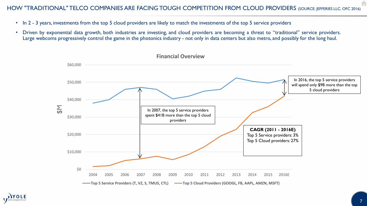
HOW "TRADITIONAL" TELCO COMPANIES ARE FACING TOUGH COMPETITION FROM CLOUD PROVIDERS (SOURCE: JEFFERIES LLC, OFC 2016)
• In 2 - 3 years, investments from the top 5 cloud providers are likely to match the investments of the top 5 service providers
• Driven by exponential data growth, both industries are investing, and cloud providers are becoming a threat to “traditional” service providers.Large webcoms progressively control the game in the photonics industry - not only in data centers but also metro, and possibly for the long haul.
$0
$10,000
$20,000
$30,000
$40,000
$50,000
$60,000
2004 2005 2006 2007 2008 2009 2010 2011 2012 2013 2014 2015 2016E
Financial Overview
Top 5 Service Providers (T, VZ, S, TMUS, CTL) Top 5 Cloud Providers (GOOGL, FB, AAPL, AMZN, MSFT)
In 2007, the top 5 service providers
spent $41B more than the top 5 cloud
providers
In 2016, the top 5 service providers
will spend only $9B more than the top
5 cloud providers
CAGR (2011 - 2016E)
Top 5 Service providers: 3%
Top 5 Cloud providers: 27%
$M
8
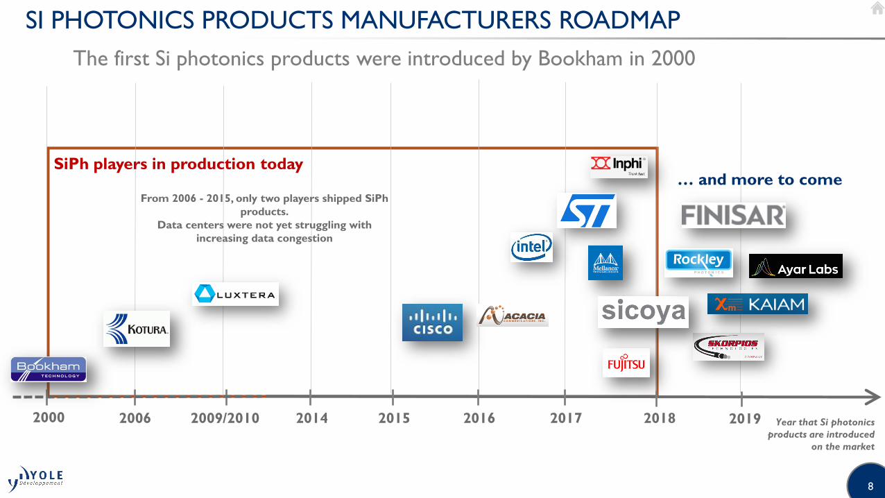
SI PHOTONICS PRODUCTS MANUFACTURERS ROADMAP
The first Si photonics products were introduced by Bookham in 2000
2006 2009/2010 2014 Year that Si photonics
products are introduced
on the market
2015 2016 2017 2018
From 2006 - 2015, only two players shipped SiPh
products.
Data centers were not yet struggling with
increasing data congestion
2000 2019
SiPh players in production today… and more to come
9
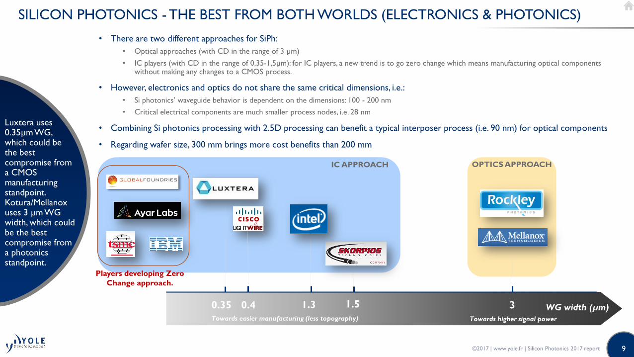
SILICON PHOTONICS - THE BEST FROM BOTH WORLDS (ELECTRONICS & PHOTONICS)
• There are two different approaches for SiPh:
• Optical approaches (with CD in the range of 3 µm)
• IC players (with CD in the range of 0,35-1,5µm): for IC players, a new trend is to go zero change which means manufacturing optical components without making any changes to a CMOS process.
• However, electronics and optics do not share the same critical dimensions, i.e.:
• Si photonics’ waveguide behavior is dependent on the dimensions: 100 - 200 nm
• Critical electrical components are much smaller process nodes, i.e. 28 nm
• Combining Si photonics processing with 2.5D processing can benefit a typical interposer process (i.e. 90 nm) for optical components
• Regarding wafer size, 300 mm brings more cost benefits than 200 mm
Luxtera uses 0.35µm WG, which could be the best compromise from a CMOS manufacturing standpoint. Kotura/Mellanoxuses 3 µm WG width, which could be the best compromise from a photonics standpoint.
©2017 | www.yole.fr | Silicon Photonics 2017 report
30.35 WG width (µm)1.3 1.50.4
Towards higher signal powerTowards easier manufacturing (less topography)
IC APPROACH OPTICS APPROACH
Players developing Zero
Change approach.

10
EXCITEMENT IS HIGH BUT IT IS STILL A MODEST MARKET
• Acacia capitalization exceeded $1.7B (Oct 2016)
• The total of private funding + acquisition total is more than $3B over past 5 years
• But the 2016 Silicon Photonics market value was less than $150M.
2017 Photonics & SiPh
transactions ~$3B
2017 SiPh revenues <
$150M

11
CONCLUSIONS
• Photonics technologies is today driven by GAFAMs.
• Today’s chip market value is still small, but more players are coming:
• After 16 years of development, Intel has successfully penetrated this application
• It shares the current market with Luxtera, leader number 1.
• New startups and more and more products reaching the market.
• Encouraging signs in terms of growing investments from the VC community.
• Si photonics is at the maturity level of the electronics industry in the 80-90s. There are still challenges
to overcome: laser source, packaging, design, supply chain, manufacturability.
• Besides Data Centres, some interesting applications could follow.