From Pencil Lead to Relativistic Quantum Physicskane/pedagogical/295lec1.pdf · From Pencil Lead to...
18
From Pencil Lead to Relativistic Quantum Physics or Electronic phenomena in mesoscopic structures • Lecture #1: Overview • Lecture #2: Quantum Transport in Solids • Lecture #3: Quantum Theory of Graphene
-
Upload
truongthien -
Category
Documents
-
view
218 -
download
1
Transcript of From Pencil Lead to Relativistic Quantum Physicskane/pedagogical/295lec1.pdf · From Pencil Lead to...

From Pencil Lead to Relativistic Quantum Physics
or Electronic phenomena in mesoscopic structures
• Lecture #1: Overview
• Lecture #2: Quantum Transport in Solids
• Lecture #3: Quantum Theory of Graphene

Why Study ElectronicMaterials and Devices?
1. The Practical

Why Study ElectronicMaterials and Devices?
2. The FundamentalA laboratory for the study of quantum manybody physics
• Collective behavior• Symmetry breaking• Role of electron electron interactions• Role of disorder• Emergent low energy behavior:
- emergent “quasiparticles”- topological order

The TransistorBardeen, Brattain, Shockley, 1947Nobel Prize 1956
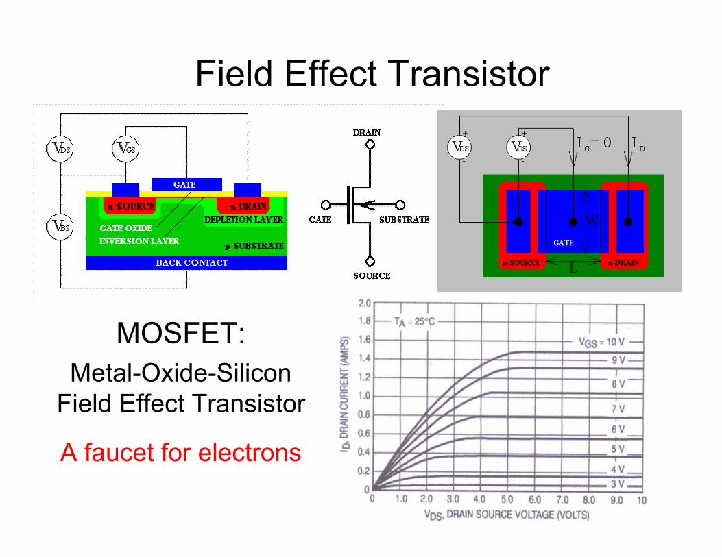
Field Effect Transistor
MOSFET:Metal-Oxide-Silicon
Field Effect Transistor
A faucet for electrons

Moore’s Law
The number of transistors on a chip doublesapproximately every two years
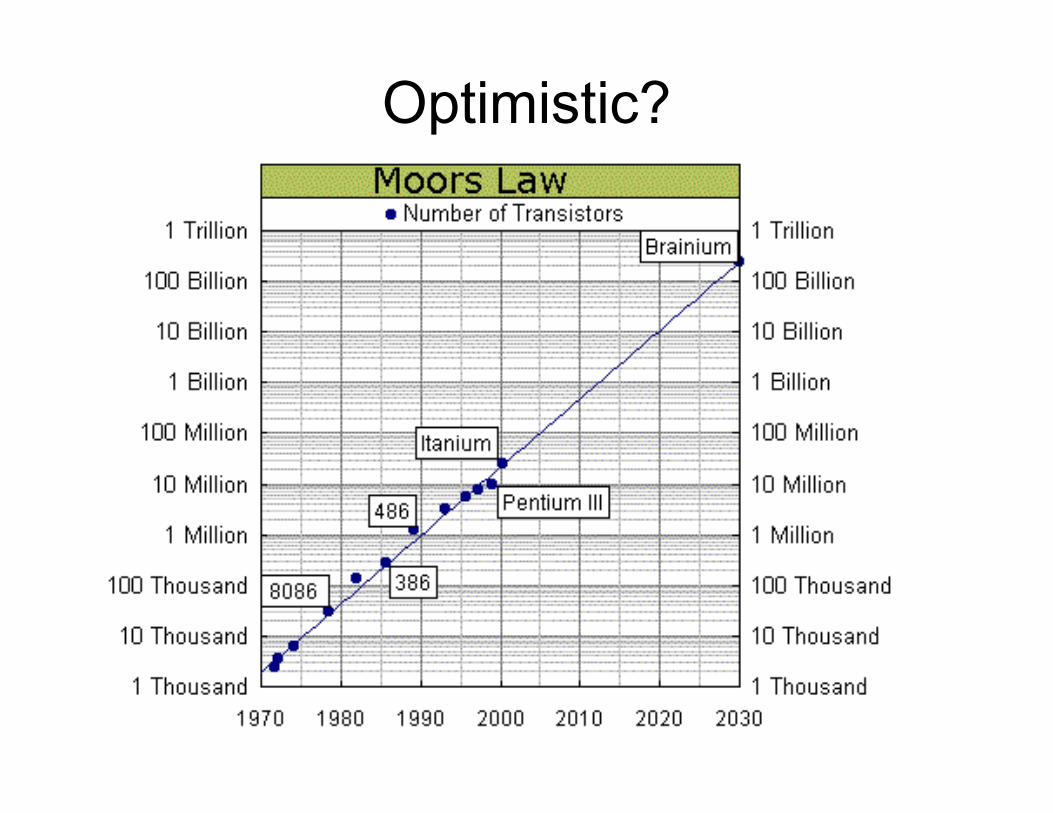
Optimistic?

Macroscopic: big things
Classical physics dominates:
V = IR ; R = ρ L/A ; Drude model: electrons ~ billiard ballsρ ~ m/(ne2τ)
~ 1 cm
Microscopic: atoms & molecules
Quantum physics dominates:
H Ψn = En Ψn
~ 1 Å = 10-8 cm

Mesoscopic
• Many atoms, but quantum physics plays a fundamental role
• Quantum effects are important for systems smaller than the thermal decoherencelength L < Lϕ(T)
• Small size OR Low temperature

Flatland ... (1980’s)Semiconductor Heterostructures : “Top down technology”→ Two dimensional electron gas (2DEG)
Ga As
AlxGa1-x As
2DEGz
V(z)
∆E ~ 20 mV ~ 250°K
2D subband
conduction bandenergy
Fabricated with atomic precision using MBE. 1980’s - 2000’s : advances in ultra high mobility samples
z

2D to 1D : Quantum Wires (1990’s):1D for E < ∆E: the 1D subband spacing
1. Split Gate Devices: (Tarucha et al. 95)
∆E ~ 5 meV
2. Cleaved Edge Overgrowth (Yacoby et al. 96)
∆E ~ 20 meV
2
2~2 *
Em L
∆

Molecular scale confinement (1990’s-2000’s)“Bottom up technology”
1. 2 Dimensions : GrapheneGraphite
• Graphene = single layer of graphite A unique 2D electronic material
• Structural Rigidity due to strong in plane bonds• Electrical Conductivity due to π electrons• Purely 2 Dimensional at room temperature

Isolating Single Planes of Graphene
Philip Kim (Columbia) Zhang et al. APL 2004
“Nanopencil” on AFM cantileverdeposits ~ 15 layer graphite films
Andre Geim (Manchester)Novoselov et al. Science 2004
Individual layers on SiO2 prepared by mechanical exfoliation.
SEM

2. 1 Dimension : Carbon Nanotubes
~ 1 µm
~ 1 nm
A Molecular Quantum Wire ∆E ~ 1 eV ~ 104 K
Graphene wrappedinto a cylinder
“rope” TEM
single tube STM AFM

The Hall EffectA tool for characterizing an electronic device
Force: ( v )e mF F F q E B= + = + ×
vy x zE B=Electric Field (Fy=0):
Current density:q = charge of carriern = carrier density
vx xJ nq=
yxy
x
E BJ nq
ρ = =Hall Conductivity
The Hall conductivity measures• The density of the mobile charge carriers• The sign of the charge carriers (e<0!)
ρxy
B

The Quantized Hall Effect
Von Klitzing,1981 (Nobel 1985)
Hall effect in 2DEG MOSFET at large magnetic field
• Quantization:
• Quantum Resistance:
• Explained by quantum mechanics of electrons in a magnetic field
/xy QR nρ =2/ 25.812 807 kQR h e= = Ω
n = integer accurate to 10-9 !

Fractional Quantized Hall EffectTsui, Stormer and Gossard 1982
Stormer, Laughlin, Tsui1998 Nobel Prize
• Higher Magnetic fields, Higher quality samples
• Quantization:
• Explained by Laughlin (1982):- Collective behavior of a “quantum fluid”- Emergent “quasiparticles” with fractional charge e/q
( / )xy Qp q Rρ =

Next Time:Quantum Transport in Solids
• Waves and particles in quantum mech.
• Quantization in atoms
• Metals vs Insulators : Energy gap
• Emergent particles in a solid
• Landau quantization in a magnetic fieldand the quantum Hall effect