From macro to micro: multi-scale study of plasmonic ...
29
From macro to micro: multi-scale study of plasmonic nanocoating self-assembled on multijunction bulk solar cells Dan Su Southeast University Xiao-Yang Zhang Southeast University Lei Lv Southeast University Huan-Li Zhou Southeast University Shan-Jiang Wang Southeast University Yi Yang Southeast University Jing-Yuan Wu Donghua University Ning Zhao Southeast University Tong Zhang ( [email protected] ) Southeast University Article Keywords: Ag@SiO2 core-shell nanostructures, Self-assembly method, Multijunction solar cell, Submicrometer-scale photoelectrical response Posted Date: November 13th, 2020 DOI: https://doi.org/10.21203/rs.3.rs-105732/v1 License: This work is licensed under a Creative Commons Attribution 4.0 International License. Read Full License
Transcript of From macro to micro: multi-scale study of plasmonic ...

From macro to micro: multi-scale study ofplasmonic nanocoating self-assembled onmultijunction bulk solar cellsDan Su
Southeast UniversityXiao-Yang Zhang
Southeast UniversityLei Lv
Southeast UniversityHuan-Li Zhou
Southeast UniversityShan-Jiang Wang
Southeast UniversityYi Yang
Southeast UniversityJing-Yuan Wu
Donghua UniversityNing Zhao
Southeast UniversityTong Zhang ( [email protected] )
Southeast University
Article
Keywords: Ag@SiO2 core-shell nanostructures, Self-assembly method, Multijunction solar cell,Submicrometer-scale photoelectrical response
Posted Date: November 13th, 2020
DOI: https://doi.org/10.21203/rs.3.rs-105732/v1
License: This work is licensed under a Creative Commons Attribution 4.0 International License. Read Full License
From macro to micro: multi-scale study of plasmonic nanocoating self-
assembled on multijunction bulk solar cells
Dan Su1,&, Xiao-Yang Zhang2,3,&, Lei Lv2,Huan-Li Zhou2, Shan-Jiang Wang2, Yi Yang2, Jing-Yuan
Wu4, Ning Zhao1,2,3, Tong Zhang1,2,3, *
1. Key Laboratory of Micro-Inertial Instrument and Advanced Navigation Technology, Ministry of
Education, School of Instrument Science and Engineering, Southeast University, Nanjing, 210096,
People's Republic of China
2. Joint International Research Laboratory of Information Display and Visualization, School of
Electronic Science and Engineering, Southeast University, Nanjing, 210096, People's Republic of
China.
3. Suzhou Key Laboratory of Metal Nano-Optoelectronic Technology, Southeast University Suzhou
Campus, Suzhou, 215123, People's Republic of China
4. Photonics Laboratory and Institute of Functional Materials, College of Science, Donghua University,
Shanghai, 201620, People's Republic of China
& These authors contributed equally to this work and should be considered co-first authors
* Corresponding author, E-mail: [email protected]
Nanophotonics pours into new opportunities to achieve ultrahigh-efficiency solar cells, attracting
tremendous interests from photovoltaic research and industry. Plasmonic nanostructures, enabling
strong light-matter interaction at the nanoscale, have been widely used for efficiency enhancement in
thin-film solar cell devices based on plasmonic near-field effects. Unlike thin-film device cases, we
found forward scattering and inter-particle coupling engineering of subwavelength plasmonic
nanostructures are the key to enhance the efficiency of bulk multijunction solar cells (MJSCs). As a
proof of concept, we studied the plasmonic enhancement of Ag@SiO2 nanocoating self-assembled on
InGaP/GaInAs/Ge MJSCs at both macro and micro scales. From the macro measurements, the
experimental enhancement of Ag@SiO2 core-shell nanostructure could be well-matched with the
simulational results, where strong forward scattering and suppressed interparticle coupling could be
simultaneously achieved by employing ~ 22 nm SiO2 shell layer. Using a double excitation method
under an infinity optical microscope, we directly observed multi-wavelength uniform photocurrent
enhancements on MJSCs at a submicrometer scale. This study will provide an effective strategy and
opening up new opportunities to explore high-efficient MJSCs using nanophotonics.

Key words: Ag@SiO2 core-shell nanostructures; Self-assembly method; Multijunction solar cell;
Submicrometer-scale photoelectrical response
Nanophotonics is believed to have great potential in realizing ultrahigh-efficiency solar cells, which
arouses attention both from academia and industry interest1. With the capability to interact with
photons strongly at the subwavelength scale, plasmonic nanostructures (such as Au, Ag nanoparticles)
have been widely applied to enhance thin-film solar cells2-5. Different physical explanations are
proposed, including localized light concentration, scattering into the active layer, scattering into guided
modes, plasmonic hot-electron effects, plasmon resonant energy transfer, or synergistic effects4,6-12.
Among other things, the primary consideration in thin-film solar cells is to make full use of the near-
field effects7,8,11,13,14. MJSCs, consisting of two or more staked junctions of semiconductors in series
connection, have been verified as a viable approach to converting wide-spectral solar energy efficiently
into electricity and hold the record for the highest solar conversion efficiency15. When integrating
plasmonic structures with the bulk MJSCs, the interaction between nanostructures and solar cells
shows some features different from thin-film solar cells. First, the active layer of MJSC is too thick to
put into the subwavelength near-field region of plasmonic nanostructures. Besides, the parasitic
absorption and directional scattering of nanostructures should be carefully considered since the bulk
solar cells already covert the photons into electrons with high efficiency16. It has been demonstrated
that Ag and Au nanostructures are difficult to enhance the efficiency of the bulk solar cell due to their
absorption losses in the visible region according to the previously reported results16-18. One potential
strategy is to reduce plasmonic absorption losses using Al nanostructures with lower absorption in the
visible range, which was demonstrated useful in specific circumstances through numerical simulation16.
Another potential strategy is to enhance the forward scattering of plasmonic nanostructures on MJSCs,
which has not been studied to the best of our knowledge.
Compared to metallic nanostructures, metal-dielectric composite nanostructures provide more
versatile control over optical, electronic, and chemical properties13,19,20. For example, a thin-layer shell
may reduce nanoparticles' recombination effects or promote carrier transportation21-23. Besides, the
stability of core-shell materials increases due to the chemical and thermal inertness of the shell
material24-26. In thin-film solar cells, shell thicknesses of less than 10 nm are usually adopted to realized
large localized electromagnetic field and controllable carrier transportation properties13,22,23. However,
the interaction mechanism between metal-dielectric core-shell nanostructures and the high-efficiency

MJSCs was still unexplored.
The difficulty partly originates from the large-scale fabrication method to organize nanometer-sized
metal-dielectric composite nanostructures into centimeter-sized macro nanocoatings for solar cells.
Top-down techniques face problems in the fabrication of three dimensions (3D) and multi-material
nanostructures, limiting the enhancement research5. While bottom-up techniques, such as self-
assembly methods, show advantages over shape control and multi-composite synthesis, benefiting
from the chemically synthesized nanoparticles27-33. Nevertheless, the nanostructures using bottom-up
approaches usually feature random particle distribution. The aggregation of nanoparticles and the
resultant coupling effect are unavoidable, resulting in a deterioration of the efficiency of the devices34.
In this account, interparticle coupling engineering in the self-assembly nanocoatings may be a solution
to this problem.
Moreover, direct visualization strategies of the photoelectrical response of MJSCs at the
submicrometer scale are still to be developed. Micro-region measurements have been demonstrated as
useful strategies for direct optical or electrical characterization of plasmonic nanostructures at the
nanoscale35-37. For example, the insight into plasmonic nanostructures' unique optical properties such
as nonlocal effects38, strong-coupling regime39, electrically driven plasmonic sources40, and
inhomogeneous plasmonic field41 have been studied at the single-particle level using the micro-region
spectroscopy. Micro-region scanning photocurrent microscopy (SPM), using a focused laser beam as
the excitation, has been used to study the response of single-junction p-n junction devices34,42-44 and
plasmonic hot-electron photodetectors 45,46. Nevertheless, when applied to MJSCs, limited by a series-
connection condition, a single laser beam could not give a net photocurrent. Different illumination and
testing strategies are needed.
Herein, we present the self-assembly of plasmonic Ag@SiO2 core-shell nanocoating for efficiency
enhancement on high-efficiency bulk InGaP/GaInAs/Ge MJSCs. We describe the device structure,
investigate the plasmonic resonance properties (both near-field and far-field) and the response of the
MJSCs with a single core-shell nanostructure with different shell thickness, demonstrate the self-
assembly strategy of Ag@SiO2 core-shell nanostructures, and make a comparison between
experimental random-distributed coating enhancement and simulational periodic array enhancement.
We also show that multi-wavelength enhancement results of the Ag@SiO2 core-shell nanocoating can
be directly observed under an infinity optical microscope with a double excitation strategy. Further,

we predict the relative enhancement could be reached with optimized structural parameters.
Results
Ag@SiO2 core-shell nanostructures for plasmon-enhanced MJSCs. The proposed device structure
of InGaP/GaInAs/Ge MJSCs is shown schematically in Fig. 1a, where the Ag@SiO2 core-shell
nanostructure is put upon the window layer of the MJSCs devices. We first simplified the model to a
single Ag@SiO2 nanostructure with different shell thickness (𝑡𝑡𝑠𝑠ℎ𝑒𝑒𝑒𝑒𝑒𝑒 ) atop InGaP-GaAs-Ge MJSCs
(details are shown in Supplementary Fig. 1), where the solar cell area 𝑊𝑊2 was set to 10-folds of the
projected area of the Ag@SiO2 nanostructure. We calculated the all-optical simulation results using
the 3D finite element method (FEM) under the assumption that internal quantum efficiency equal to
100%16, and modeling details will be introduced in the Methods section. Considering the current of
InGaP-GaAs-Ge MJSCs is constrained by the top and middle subcells16, we only studied the optical
responses of the upper two subcells.
As shown in Fig. 1b, if there is no shell (namely, 𝑡𝑡𝑠𝑠ℎ𝑒𝑒𝑒𝑒𝑒𝑒 = 0), the current density in the top cell
would not increase, which is similar to the previous results17. As 𝑡𝑡𝑠𝑠ℎ𝑒𝑒𝑒𝑒𝑒𝑒 increases from 2 nm to 90 nm,
short-circuit current density of the top cell (𝐽𝐽𝑡𝑡𝑡𝑡𝑡𝑡 𝑐𝑐𝑒𝑒𝑒𝑒𝑒𝑒) shows an increasing tendency first, followed by a
dropping tendency with a maximum current density at a shell thickness of 50 nm. While the short-
circuit current density of the middle cell (𝐽𝐽𝑚𝑚𝑚𝑚𝑚𝑚𝑚𝑚𝑒𝑒𝑒𝑒 𝑐𝑐𝑒𝑒𝑒𝑒𝑒𝑒 ) increases monotonically in this range. And 𝐽𝐽𝑚𝑚𝑚𝑚𝑚𝑚𝑚𝑚𝑒𝑒𝑒𝑒 𝑐𝑐𝑒𝑒𝑒𝑒𝑒𝑒 is larger than 𝐽𝐽𝑡𝑡𝑡𝑡𝑡𝑡 𝑐𝑐𝑒𝑒𝑒𝑒𝑒𝑒 at all conditions, so we conclude that 𝐽𝐽𝑡𝑡𝑡𝑡𝑡𝑡 𝑐𝑐𝑒𝑒𝑒𝑒𝑒𝑒 determines the short-
circuit current density (𝐽𝐽𝑠𝑠𝑐𝑐) of the series-connected MJSC with Ag@SiO2 nanostructures. To elucidate
the enhancement mechanism, we compared the scattering intensity patterns for different shell thickness
in Fig. 1c-d (3D scattering pattern at the wavelengths of 375 nm, 410 nm, and 450 nm referred to
Supplementary Movies 1, 2, and 3, respectively). As illustrated, the scattering intensity of the
Ag@SiO2 could be modulated by the shell thickness. In our case, the maximum forward scattering
(scattering into the MJSC) intensity (~1000 folds larger than the intensity of the bare Ag nanosphere)
was achieved at 𝑡𝑡𝑠𝑠ℎ𝑒𝑒𝑒𝑒𝑒𝑒 = 50 nm, while a thicker shell would lead to increased backward scattering
intensity.

Fig. 1 Plasmonic enhancement by Ag@SiO2 nanostructures on MJSCs. a Schematic structure of Ag@SiO2
atop a GaInP-GaInAs-Ge MJSC. b Calculated current density of top and middle solar cell with different 𝑡𝑡𝑠𝑠ℎ𝑒𝑒𝑒𝑒𝑒𝑒. Calculated normalized scattering intensity patterns for the scattering planes parallel (c) and perpendicular (d) to
the polarization of the incident wave (𝜆𝜆 = 410 𝑛𝑛𝑛𝑛). e Calculated Ag@SiO2 absorption under different 𝑡𝑡𝑠𝑠ℎ𝑒𝑒𝑒𝑒𝑒𝑒 . Calculated relative EQE enhancement of top (f) and middle (g) cell under different 𝑡𝑡𝑠𝑠ℎ𝑒𝑒𝑒𝑒𝑒𝑒.
Meanwhile, the absorption of Ag nanoparticle (Fig. 1e) and the relative external quantum efficiency
(EQE) enhancement (Fig. 1f-g, Supplementary Fig. 2 for EQE original data) of subcells (top cell and
middle cell) were calculated. The absorption peak of Ag@ SiO2 nanostructures redshifts from 370 nm
to 410 nm with the increasing 𝑡𝑡𝑠𝑠ℎ𝑒𝑒𝑒𝑒𝑒𝑒 , while absorption intensity slightly changes and reaches a
maximum when 𝑡𝑡𝑠𝑠ℎ𝑒𝑒𝑒𝑒𝑒𝑒 = 50 nm. Nevertheless, we notice that the EQE drop of the top cell near the
Ag absorption region is the smallest when 𝑡𝑡𝑠𝑠ℎ𝑒𝑒𝑒𝑒𝑒𝑒 = 50 nm, indicating more incident photons are
preferentially scattering into the top cell near the plasmonic resonance wavelength region with the
assistance of 50 nm SiO2 shell. We also notice when 𝑡𝑡𝑠𝑠ℎ𝑒𝑒𝑒𝑒𝑒𝑒 further increase to 90 nm, although the
absorption of Ag is gradually reduced, the EQE decreases near the plasmonic resonance region,

suggesting more photons are scattering backward into the air. Meanwhile, the EQE of the middle solar
cell is enhanced almost at all wavelengths and all thicknesses. Therefore, a single Ag@SiO2
nanostructure could improve the efficiency of the MJSC through scattering management regardless of
the existence of the plasmonic absorption.
To study the influence of aggregates on the response of MJSCs, we simulated different aggregation
types with the same surface coverage (~48 NP/μm2) of bare Ag nanospheres and Ag@SiO2 core-shell
nanostructures on the MJSCs. As shown in Fig. 2a, type Ⅰ is monodisperse, represented by a periodic
array with the same interparticle distance. Type Ⅱ, Ⅲ, and Ⅳ are dimer, tetramer, and trimer with
single nanostructure atop as featured structures. The electrical field distributions of the Ag nanospheres
and Ag@SiO2 nanostructures are also depicted in Fig. 2a. Localized electric field enhancement up to
270 is observed at the Ag nanospheres gap, indicating the strong interparticle coupling without the
shell. By stark contrast, the maximum electric intensity in Ag@SiO2 aggregates is ~11, which means
the plasmonic coupling is suppressed by ~22 nm SiO2 shell. The absorption spectra further show the
plasmonic coupling of Ag and Ag@SiO2 nanostructures, where absorption spectra of Ag aggregates
show multiple absorption peaks while Ag@SiO2 aggregates show similar absorption curves compared
to the monodisperse condition (Fig.2b and Fig. 2e). The EQE of the top and middle solar cell were
calculated to study the spectral response of different structures (Fig. 2c and Fig. 2f). Interestingly,
unlike Ag nanosphere aggregates, Ag@SiO2 nanostructures studied here yields similar normalized
EQE spectra of the top cell. To estimate the efficiency enhancement of InGaP-GaAs-Ge MJSCs under
the solar spectrum of AM1.5G, we calculated the top and middle subcells' current density in Fig. 2d
and Fig. 2g. Although the 𝐽𝐽𝑚𝑚𝑚𝑚𝑚𝑚𝑚𝑚𝑒𝑒𝑒𝑒 𝑐𝑐𝑒𝑒𝑒𝑒𝑒𝑒 increases slightly for Ag nanospheres aggregates, the 𝐽𝐽𝑡𝑡𝑡𝑡𝑡𝑡 𝑐𝑐𝑒𝑒𝑒𝑒𝑒𝑒 decreases when aggregation happens. On the contrary, both 𝐽𝐽𝑡𝑡𝑡𝑡𝑡𝑡 𝑐𝑐𝑒𝑒𝑒𝑒𝑒𝑒 and 𝐽𝐽𝑚𝑚𝑚𝑚𝑚𝑚𝑚𝑚𝑒𝑒𝑒𝑒 𝑐𝑐𝑒𝑒𝑒𝑒𝑒𝑒 of Ag@SiO2
aggregates increase. Thus, the Ag@SiO2 core-shell aggregates yield similar enhancement results as
monodispersed core-shell nanostructures, which means the self-assembly Ag@SiO2 core-shell
nanocoating will result in a robust plasmonic enhancement.

Fig. 2 3D FEM simulation of different types of aggregates atop of InGaP-GaAs-Ge MJSCs. a Illustrations
of different type aggregates and the electrical field distribution in Ag (at 640 nm) and Ag@SiO2 (at 410 nm)
nanostructures. b Calculated Ag absorption. c Calculated normalized EQE of top subcell with Ag nanostructures.
d Calculated Jsc of top subcell and middle subcell with Ag nanostructures. e Calculated Ag@SiO2 absorption. f
Calculated normalized EQE of top subcell with Ag@SiO2 nanostructures. g Calculated current densities of top
subcell and middle subcell with Ag@SiO2 nanostructures.
Nanocoating fabrication and characterization. As proof of concept, we synthesized the Ag@SiO2
experimentally, and the characteristic transmission electron microscopy (TEM) graphs in
Supplementary Fig. 3 shows both Ag cores and Ag@SiO2 core-shell nanostructures are large-scale
monodispersed and well-dispersed. The typical diameter of Ag cores is ranged from 22 nm to 34 nm,
with a mean diameter of 29 nm. Besides, the thickness of the SiO2 shell is in the range of 16 to 30 nm,

with a mean thickness of 22 nm. Ag@SiO2 core-shell nanostructures' surfaces are negative-charged
and abundant with -OH, which facilitate the bonding with poly-L-lysine through electrostatic forces
or a dehydration reaction47. The self-assembly process involves the following steps (Fig. 3a). First, the
InGaP/GaInAs/Ge MJSC were inverted floated (supported by the water's surface tension) upon the
poly-L-lysine solution for 5 minutes, enabling the absorption of the front side only. Then, excess poly-
L-lysine molecules were washed by ultra-pure water to ensure that no optical-thick layer exists. After
that, the MJSC was immersed in the ethanol solution of Ag@SiO2 core-shell nanostructures for
different times (1,5 and 15 minutes), followed by washing with ultra-pure water to remove the unbound
nanostructures. We performed an element analysis of MJSCs after the self-assembly process. Energy-
dispersive X-ray spectrometer (EDS) results of the bare MJSC and the MJSC after 15 min
nanostructure assembly are provided in Supplementary Fig. 3. We found Ag and Si elements in the
MJSC after the self-assembly process, further verifying the successful self-assembly of Ag@SiO2
core-shell nanostructures. We have already proved that poly-L-lysine treatment has a negligible effect
on the solar cells' electrical parameters in Reference 47. To verify the existence of poly-L-lysine, we
examined element N, which is a characteristic element in poly-L-lysine. A trace amount of N element
is found in the sample after the self-assembly process, while no N element was detected in the bare
MJSC.
To determine the surface coverage of Ag@SiO2 nanostructures atop InGaP/GaInAs/Ge MJSCs, we
analyzed the scanning electron microscopy (SEM) characterizations shown in Fig. 3b-d. As time
increases from 1 min to 15 min, the distribution density of Ag@SiO2 core-shell nanostructures
continually increase. However, when the assembly time further increases to 30 min, there is no
perceptible increase in distribution density (Supplementary Fig. 4). SEM graphs near the grid regions
and the large-area views provided in Supplementary Fig. 5 show the large-area consistency at the
whole surface of MJSCs. Further statistical analysis of SEM graphs supplies the surface coverage data
of Ag@SiO2 core-shell nanocoatings on MJSCs. The assembly time of 1 min, 5 min, and 15 min yields
~4, ~18, and ~47 nanoparticles per square micrometer (NP/μm2), respectively (Fig. 3e). Additionally,
single-layer dimers and multimers exist in all of the samples. Compared with monodispersed TEM
graphs, it indicates the introduction of those aggregates may result in the self-assembly process. We
determined the structural types in the self-assembly layer (Fig. 3f). Only 50%-70% of structures are
single, while the multimer ratio increased along with the increased surface coverage of nanostructures.

Fig. 3 SEM analysis of Ag@SiO2 core-shell nanocoatings. SEM image of different self-assembly time 1
min(b), 5 min(c), and 15 min(d). e Surface coverage analysis of the self-assembly nanocoating under different
times. f Structural type analysis of the Ag@SiO2 nanostructures in the self-assembly nanocoating.
Macro photoelectrical response measurement. Aimed to confirm the robust enhancement results
experimentally, we compared the enhancement between the experimental random distributed
nanostructures and the simulational periodic nanostructure arrays (Fig. 4). To fully recover the real
condition, we first let the surface coverage similar to our self-assembly samples. The simulational
period is set to be 500 nm (W1), 230 nm (W2), 145 nm (W3), corresponding to a surface coverage of
4, ~18, and ~48 NP/μm2, respectively. As shown in Fig. 4b and Fig. 4e, when the wavelength exceeds
450 nm, the EQE of the top subcell increases with the assembly time. However, at the wavelength
region near plasmonic resonance of Ag@SiO2 nanostructures, the top subcell EQE reduces along with
the increased assembly time. That is to say, near the plasmonic resonance wavelength, even though the
strong antireflection happens (Supplementary Fig. 6), strong absorption of the Ag@SiO2 nanocoating
deteriorates the EQE. So, there is a tradeoff between the photoelectrical responses at different

wavelengths, similar to the previously reported results using Au or Ag nanoparticles17. Besides, the
EQE of the middle subcell slightly increased with the adding of nanostructured layers at the entire
wavelength range. We also normalized the EQE of the MJSCs with a nanostructured layer to the Ref
device (Fig. 4c and Fig. 4f). Although the EQE curve shows some difference between experimental
and simulational results due to optical constants difference from doping, the normalized EQE curves
show an excellent consistency between experiment and simulation. As a result, the 𝐽𝐽𝑠𝑠𝑐𝑐 data derived
from EQE data also show a similar increasing trend (Fig. 4d and Fig. 4g). With the self-assembly time
increases, the experimental 𝐽𝐽𝑠𝑠𝑐𝑐 increases from 9.76 mA/cm2 to 9.79 mA/cm2 (1 min), 9.93 mA/cm2
(5 min) and 10.17 mA/cm2 (15 min), with relative enhancement of 0.31% (1 min), 1.74% (5 min) and
4.20% (15 min). The simulational 𝐽𝐽𝑠𝑠𝑐𝑐 varies from 10.49 to 10.55 mA/cm2 (W1), 10.65 mA/cm2 (W2),
10.79 mA/cm2 (W3), and the relative enhancement are 0.57% (W1), 1.53% (W2), and 2.86% (W3).
Thus, we conclude that the aggregates in self-assembly methods did not alleviate the enhancement.
We also verify that the simulational periodic arranged Ag@SiO2 nanostructures could be used to
predict the enhancement of experimental random distributed Ag@SiO2 nanostructures, with a shell
thickness of more than 20 nm.
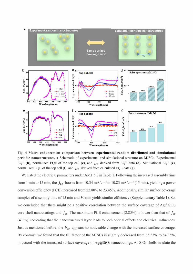
Fig. 4 Macro enhancement comparison between experimental random distributed and simulational
periodic nanostructures. a Schematic of experimental and simulational structure on MJSCs. Experimental
EQE (b), normalized EQE of the top cell (c), and 𝐽𝐽𝑠𝑠𝑐𝑐 derived from EQE data (d). Simulational EQE (e),
normalized EQE of the top cell (f), and 𝐽𝐽𝑠𝑠𝑐𝑐 derived from calculated EQE data (g).
We listed the electrical parameters under AM1.5G in Table 1. Following the increased assembly time
from 1 min to 15 min, the 𝐽𝐽𝑠𝑠𝑐𝑐 boosts from 10.34 mA/cm2 to 10.83 mA/cm2 (15 min), yielding a power
conversion efficiency (PCE) increased from 22.80% to 23.45%. Additionally, similar surface coverage
samples of assembly time of 15 min and 30 min yields similar efficiency (Supplementary Table 1). So,
we concluded that there might be a positive correlation between the surface coverage of Ag@SiO2
core-shell nanocoatings and 𝐽𝐽𝑠𝑠𝑐𝑐. The maximum PCE enhancement (2.85%) is lower than that of 𝐽𝐽𝑠𝑠𝑐𝑐 (4.7%), indicating that the nanostructured layer leads to both optical effects and electrical influences.
Just as mentioned before, the 𝑉𝑉𝑡𝑡𝑐𝑐 appears no noticeable change with the increased surface coverage.
By contrast, we found that the fill factor of the MJSCs is slightly decreased from 85.53% to 84.35%,
in accord with the increased surface coverage of Ag@SiO2 nanocoatings. As SiO2 shells insulate the

Ag nanospheres and the MJSC, recombination effects of the nanostructures almost eliminate. It
suggests the main reason of the deterioration in the fill factor may lie in the inevitable assembly of
Ag@SiO2 core-shell nanostructures on the electrodes.
Table 1 Electrical parameters of MJSCs with different self-assembly time
Description Voc(V) Jsc(mA/cm2) Fill factor(%) Efficiency(%)
Ref 2.58±0.01 10.34±0.17 85.53±0.28 22.80±0.36
1 min 2.56±0.01 10.51±0.06 84.94±0.06 22.93±0.12
5 min 2.56±0.01 10.71±0.08 84.65±0.08 23.25±0.14
15 min 2.56±0.01 10.83±0.10 84.35±0.16 23.45±0.19
Micro-region photoelectrical response measurement. To unveil the enhancement effects of
Ag@SiO2 core-shell nanocoatings directly on the micro-scale, we designed and built a micro-region
photoelectrical response measurement system (Supplementary Fig. 7). The submicrometer-scale SPM
measurement is based on an infinity optical microscope with a double excitation strategy described in
Fig. 4a. Due to the current-constrained condition in series packed MJSCs, all other subcells are
supposed to supply larger currents when one subcell is tested. The wide-spectral light from a tungsten
halogen lamp processed by a Kohler illuminating path and a designed color filter act as the biased light
for MJSCs. As an example, for the photocurrent measurement of the InGaP subcell in a triple-junction
InGaP/GaInAs/Ge solar cell, the wide-spectral light is filtered by an 800 nm long-pass filter for the
excitation of the GaInAs and Ge solar cell. Frequency-modulated wavelength-tunable laser functions
as the signal light, which power could be delicately nudged to ensure the current-limited condition. A
home-made MJSC microscopic holder and 4-wire connection are used to test the electrical signal. The
modulated photocurrent is collected and processed by a current preamplifier, a lock-in amplifier, and
a digital source-measure unit (SMU). Moreover, a biased voltage is provided from the SMU. The
focused laser and biased light can be scanned using a piezoelectric travel translation stage with X/Y
motors when SPM measurements are performed. Controlled by a home-designed Labview program,
the modules mentioned above enable efficient in-situ micro-region optical and SPM measurements of
MJSCs.
The device with a self-assembly time of 5 min was investigated for relative uniform distribution
with fewer multilayer aggregates. We set a micro-region with an area of 8 × 8 μm as the region of
interest. Before testing, we partly wiped out the Ag@SiO2 core-shell nanocoating using non-dusting

whipping paper, aiming to get a micro-region partly covered by the nanocoating and partly bare. In
this way, we enable direct observation of the enhancement induced by the core-shell nanocoating. Fig.
4b-c show the brightfield and darkfield optical images of the device's surface, and the corresponding
optical path is shown in Supplementary Fig. 8. The white frame lines define the boundary of the
nanocoating and bare surface. We can discern the region with/without nanocoating from the brightfield
image, but the negligible scattering from the monolayer nanostructured layer makes little difference in
the darkfield image.
Fig. 5 Micro-region SPM study for InGaP-GaAs-Ge MJSCs with the Ag@SiO2 core-shell nanocoating
(assembly time, 5 min). a Schematic graph of the submicrometer-scale photoelectrical response measurement
for MJSCs. The brightfield (c) and darkfield images (d) of the MJSCs with partly-removed Ag@SiO2 core-shell
nanocoating (assembly time, 5 min). The Ag@SiO2 nanostructures in the region surrounded by the white frame
lines were wiped out. d The wavelength-dependent EQE relative variation images of the same region as the
optical images shown in a-b. e EQE relative variation analysis of the background (region 1) and the Ag@SiO2
core-shell nanocoating (region 2) under the excitation of different wavelengths. The dashed line presents the
top subcell's macro normalized EQE curve with an assembly time of 5 min. The error bars show the absolute
variations in the specific region.
Using the proposed SPM for the MJSC, we attained the photocurrent (𝐼𝐼𝑡𝑡ℎ) mapping images (17 ×
17 pixels) for the MJSC under the laser excitation with different wavelengths. For comparison between
micro and macro measurements, we define micro EQE relative variation as ∆𝐸𝐸𝐸𝐸𝐸𝐸/𝐸𝐸𝐸𝐸𝐸𝐸𝑏𝑏𝑏𝑏𝑐𝑐𝑏𝑏, where ∆𝐸𝐸𝐸𝐸𝐸𝐸 is the difference between EQE of the location to be measured and the EQE of background

(EQEback, without nanostructured layer). Similarly, the photocurrent relative variation is (𝐼𝐼𝑡𝑡ℎ−𝐼𝐼𝑏𝑏𝑏𝑏𝑐𝑐𝑏𝑏)/𝐼𝐼𝑏𝑏𝑏𝑏𝑐𝑐𝑏𝑏 (∆𝐼𝐼𝑡𝑡ℎ/𝐼𝐼𝑏𝑏𝑏𝑏𝑐𝑐𝑏𝑏). And we transform the photocurrent maps into EQE relative variation maps with
the following relation, 𝐼𝐼𝑡𝑡ℎ = 𝑞𝑞𝑃𝑃𝑒𝑒𝑏𝑏𝑠𝑠𝑒𝑒𝑙𝑙 ∙ 𝜆𝜆ℎ𝑐𝑐 ∙ 𝐸𝐸𝐸𝐸𝐸𝐸 (1) ∆𝐸𝐸𝐸𝐸𝐸𝐸/𝐸𝐸𝐸𝐸𝐸𝐸𝑏𝑏𝑏𝑏𝑐𝑐𝑏𝑏 = ∆𝐼𝐼𝑡𝑡ℎ/𝐼𝐼𝑏𝑏𝑏𝑏𝑐𝑐𝑏𝑏 (2)
where 𝐼𝐼𝑡𝑡ℎ is the generated photocurrent, 𝑃𝑃𝑒𝑒𝑏𝑏𝑠𝑠𝑒𝑒𝑙𝑙 is the power of the laser just after the microscope
objective. To diminish the random error, we set mean 𝐼𝐼𝑡𝑡ℎ of region 1 (27 pixels) as 𝐼𝐼𝑏𝑏𝑏𝑏𝑐𝑐𝑏𝑏. Region 1
is defined as the equation 0.5𝑥𝑥 + 1 ≤ 𝑦𝑦 ≤ 0.5𝑥𝑥 + 2 (0 ≤ 𝑥𝑥, 𝑦𝑦 ≤ 8), where the origin was set as the
lower-left corner. As we have discussed, the Jsc of the top subcell mainly contributes to the current
enhancement of the whole device, so only the EQE relative variation of the top subcell is obtained (Fig.
5c). The EQE enhancement of the top subcell under different excitation wavelengths varies differently.
In the mapping images, the red color, blue color, and white color represent an increase, a decrease, and
no distinct change relative to 𝐸𝐸𝐸𝐸𝐸𝐸𝑏𝑏𝑏𝑏𝑐𝑐𝑏𝑏, respectively. The contrast between the double-sides of the
black line border in the EQE images directly displays the enhancement effect of the Ag@SiO2 core-
shell nanocoating. No noticeable enhancement or suppression was found at 450 nm, but definite
enhancements were achieved at the wavelengths longer than 480 nm with a maximum value of ~10%.
Statistical analysis was conducted to show the average enhancement and variation level of the
proposed method in Fig. 5d-f and Supplementary Table 2-3, where the area of region 2 was 2 × 2 μm
(25 pixels). In region 1, the absolute variation is ~2% at the wavelengths of 450 nm and 480 nm, near
1% (or smaller than 1%) at other wavelengths. Small changes in the background area may be related
to the nonuniformity of the surface, the fluctuation of laser power, the background noise in the current
extraction circuit, and the spectral response of the MJSC. The wavelength-dependent average
enhancement of region 2 follows the same trend with the macro EQE test, with the maximum relative
enhancement at 500 nm. Additionally, the absolute variation of region 2 is similar to that of region 1,
indicating the relatively uniform distribution of the Ag@SiO2 core-shell nanocoating.

Fig. 6 Simulation of closely packed Ag@SiO2 nanostructure array atop the MJSC. a Schematic of the
MJSC with closely packed Ag@SiO2 nanostructures. b Calculated Shell thickness-dependent current density of
top and middle solar cell; the dashed line shows the current density without nanostructure. c-d Calculated Ag
absorption and reflection of the MJSC with different shell thicknesses.e Relative 𝐽𝐽𝑠𝑠𝑐𝑐 enhancement of the MJSC
with closely packed Ag@SiO2 nanostructure array.
To explore the optimized parameters for MJSCs using Ag@SiO2 nanostructures, we simulated the
closely packed arrays of Ag@SiO2 nanostructures (Fig. 6 and Supplementary Fig. 9). The schematic
of closely packed nanostructures are shown in Fig. 6a, and we calculated the current density of the top
cell and middle cell in Fig. 6b. The results are different from the well-dispersed single particle
condition in Fig. 1b. Both 𝐽𝐽𝑡𝑡𝑡𝑡𝑡𝑡 𝑐𝑐𝑒𝑒𝑒𝑒𝑒𝑒 and 𝐽𝐽𝑚𝑚𝑚𝑚𝑚𝑚𝑚𝑚𝑒𝑒𝑒𝑒 𝑐𝑐𝑒𝑒𝑒𝑒𝑒𝑒 show inflection points (at 40 nm for 𝐽𝐽𝑡𝑡𝑡𝑡𝑡𝑡 𝑐𝑐𝑒𝑒𝑒𝑒𝑒𝑒 and
60 nm for 𝐽𝐽𝑚𝑚𝑚𝑚𝑚𝑚𝑚𝑚𝑒𝑒𝑒𝑒 𝑐𝑐𝑒𝑒𝑒𝑒𝑒𝑒). Besides, the absorption bandwidth of Ag nanocore gradually shrink with the
increased 𝑡𝑡𝑠𝑠ℎ𝑒𝑒𝑒𝑒𝑒𝑒, while the absorption intensity achieves the maximum value at a thickness of 40 nm
(Fig. 6c). Fig. 6d shows the reflectance spectra of Ag@SiO2 MJSCs with nanostructures, the lowest
reflectance located in the Ag absorption peak in the thickness range of 30 to 90 nm, and the smallest
reflectance is approaching 0%. At last, we calculated the shell thickness-dependent relative
enhancement in Fig. 6e, and we found a 𝐽𝐽𝑠𝑠𝑐𝑐 enhancement of 19.92% (from 10.49 mA/cm2 to 12.58
mA/cm2) when 𝑡𝑡𝑠𝑠ℎ𝑒𝑒𝑒𝑒𝑒𝑒 = 40 nm, which may be experimentally achieved by multiple assembly
processes or the Meyer rod method48.

Discussion
We have demonstrated that Ag@SiO2 self-assembly nanocoatings enable efficiency-boosting of
InGaP-GaAs-Ge MJSCs at macro and micro scale. We show a relatively thicker shell (about 20-50 nm)
is needed for bulk MJSC enhancement compared to the thin-film solar cell or plasmon-enhanced
spectroscopy applications. The enhancement mechanism mainly contributes to enhanced far-field
forward scattering while the near-field coupling needs to be suppressed. Based on our results, we
estimated a Jsc enhancement of 19.92% for the close-packaged Ag@SiO2 condition, comparable to the
enhancement of antireflection film techniques. Moreover, the relatively simple fabrication method and
thinner thickness make them more competitive for photovoltaic applications. We point out that the
dielectric shell could be replaced with semiconductor materials such as TiO2, ZnO49,50. We also predict
that metal-dielectric super-scattering nanostructures with designed electric and magnetic dipolar
resonances42,43 may further boost efficiency. Additionally, we emphasize the importance of the multi-
scale characterization for plasmon-enhanced MJSCs. With this strategy, not only can we compare the
macro performance of the MJSCs, but also directly observe and study the plasmonic enhancement with
a submicrometer resolution. We believe our findings will open a new path for developing ultrahigh
efficiency MJSCs using nanophotonics.
Methods
Materials. Silver nitrate (AgNO3, 99.9%), ascorbic acid (AA, >99.5%), Tetraethyl orthosilicate
(TEOS, 98%), and sodium hydroxide solution (NaOH, ≥98%) were purchased from Sigma-Aldrich.
Absolute ethanol (≥95%) and cetyltrimethylammonium bromide (CTAB, >99.0%) was purchased
from sinopharm chemical reagent Co. Ltd. Poly-L-lysine was bought from Xiya Regent. Milli-Q
Ultrapure water (resistivity>18.2 MΩ cm) was utilized in all experiments. All chemicals in the
experiment are used with no further purification. The Shanghai Institute of Space Power-Source
provided triple-junction InGaP-GaAs-Ge solar cells. The solar cells (area:3.14 cm2) were cut from a
single epitaxial wafer for similar original spectral response and efficiency.
Synthesis of Ag@SiO2 core-shell nanostructure. The Ag@SiO2 core-shell nanostructure was
synthesized using a one-pot method modified from the previous work51. Briefly, 3 mL freshly prepared
AgNO3 (0.1 M) was added to 60 mL CTAB (2.5 mM) under moderate stirring for 2 minutes, followed
by adding 4.2 mL AA (0.1 M) solution and stirring for another 5 minutes, 1.68 mL NaOH (0.5 M) was

further added and stirred for 15 minutes. After those steps, Ag nanoparticle was synthesized, an aliquot
of 1 mL was extracted and centrifuged one time before characterization. Immediately after the
synthesis of Ag nanospheres, 150 μL TEOS and 15 mL ethanol were added to the Ag nanosphere
solution, another 975 μL NaOH (0.5 M) was injected to adjust the PH of the solution to ~10.9 for
proper coating speed. The SiO2 coating process lasts about 3 hours. The resultant products were
centrifuged several times using ethanol and condensed to 5 mL for further use and characterization.
Ag@SiO2 core-shell nanostructures characterization. The Ag@SiO2 core-shell nanostructures'
structural parameters were characterized by TEM (Fei Tecnai G20) with an acceleration voltage of 200
kV, and ImageJ software was used to analyze the statistical results. The extinction spectra were
acquired from a fiber spectrometer (Nova, Ideaoptics Co Ltd). The Ag@SiO2 core-shell self-assembly
nanocoating was characterized by a scanning electron microscope (SEM, Zeiss Ultra Plus) operating
at 5 kV-10 kV. Elemental compositions of the self-assembly layer were also studied by an energy-
dispersive X-ray spectrometer (EDS).
Macro measurements of MJSCs. The electrical properties of solar cells are measured with a high-
precision SMU (Keithley 2651), and the illumination was simulated with a 1000 W xenon lamp
equipped with an AM1.5 filter (Crowntech Inc.). A standard reference cell (VLSI Standards Inc., SRC-
1000-TC-K-QZ-C) is used to calibrate. The reflection spectra of MJSCs were also taken from a fiber
spectrometer (Nova, Ideaoptics Co Ltd) coupled with an integrating sphere. The solar spectral power
density of AM1.5G is obtained from ASTM G173-03 reference spectra derived from SMARTS. The
external quantum efficiency of the MJSC was recorded with a solar cell quantum efficiency system
(PV Measurements, QEX10). Intending to discern the current contribution from each subcell, we
calculated Jsc of the top subcell and the middle subcell with the integral equation (3),
𝐽𝐽𝑠𝑠𝑐𝑐 = 𝑞𝑞 ∫ 𝑃𝑃𝐴𝐴𝐴𝐴1.5𝐺𝐺(𝜆𝜆) ∙𝜆𝜆2𝜆𝜆1 𝜆𝜆ℎ𝑐𝑐 ∙ 𝐸𝐸𝐸𝐸𝐸𝐸(𝜆𝜆)𝑑𝑑𝜆𝜆 (3)
where 𝑃𝑃𝐴𝐴𝐴𝐴1.5𝐺𝐺 is the solar spectral power density of AM1.5G, 𝑞𝑞 is the elementary charge, ℎ is the
Planck constant, c is the speed of light in free space, 𝜆𝜆 is the wavelength.
Micro-region imaging measurement. Brightfield and darkfield optical images are collected at the
same location using a Nikon inverted microscope (Ti-U) with a 100 W tungsten halogen lamp. A 100×
0.80 NA objective lens (Nikon Plan Fluor ELWD 100X) was used to collect both the bright and dark
filed images and spectra. The optical images are collected by a scientific color CCD (Qimaging

MicroPub1isher 3.3).
SPM measurement for MJSCs. SPM includes the custom-designed electrical measurement fixture,
which can be perfectly matched with Nikon dark-filed microscope and the piezoelectric travel
translation stage (TANGO Desktop, Märzhäuser). Monochromatic radiation was created through the
super-continuum white-light source (YSL Photonics, SC-PRO) and acousto-optic tunable filter (YSL
AOTF-PRO) was through an optical cage laser beam expander system and an aperture to reduce the
divergence angle of light and filtered by the color temperature filter (LB-165, Thorlabs). The mapping
length is 8 μm with a step of 500 nm. A chopper working at a frequency of 500Hz was used to get the
photocurrent, and a current preamplifier (Stanford SR570) and lock-in amplifier (Hengbing Instrument)
was used to suppress the dark current. A high-precision SMU (Keithley 2450) was used to record the
data and supply the biased voltage. The laser beam's power was recorded by a Newport 843-4-USB
power meter with a 918D-SL-OD1R Si photodetector. The focused laser's power is 450 nW, 560 nW,
505 nW, 665 nW, 965 nW, and 740 nW at the wavelength of 450 nm, 480 nm, 500 nm, 520 nm, 540
nm, and 600 nm, respectively. The focused laser and biased light's spot size is estimated as ~1.5 μm
and 300 μm.
3D FEM simulation. We used the periodic boundary conditions for the x- and y-axis for easier surface
coverage control in the simulation. Perfect matched layer (PML) conditions were applied along the z-
axis, which diminishes the unexpected reflection. Two ports between the PML layers and the device's
geometry were set for excitation (planar wave polarized in the x-direction). The permittivity of silver
was fitted using the Lorentz-Drude model52. The optical constants of SiO2, GaInAs, Ge are linearly
interpolated from the handbook53. The optical constants for AlInP, GaInP, AlGaInP, and AlGaAs are
adopted from Ref 54-57.
For the absorption of Ag@SiO2, the top cell and the middle cell can be expressed as
𝐴𝐴 = ∫ 𝜔𝜔2 𝐼𝐼𝑛𝑛�𝜀𝜀(𝜔𝜔)�𝜀𝜀0|𝐄𝐄(𝐫𝐫)|2𝑑𝑑3𝑟𝑟 𝑉𝑉 (4)
where E is the electric field intensity, 𝜀𝜀 is the dielectric of the material, 𝜀𝜀0 is the permittivity of
vacuum, and the 𝜔𝜔 is the angular frequency of light. The current density was also calculated from
equation (3) with the absorption of each subcell.
For far-field scattering pattern simulation, we used a scattering field formulation, triggered by the
background field calculated by replacing the dielectric constants of the Ag@SiO2 nanostructure

domain with the dielectric constants of the air. We further normalized the angle-distributed scattering
power by geometric cross-section area of the Ag@SiO2 for comparison of different shell thicknesses.
Data availability
The data that support the findings of this study are available from the corresponding author upon
reasonable request.
Reference
1 Polman, A. & Atwater, H. A. Photonic design principles for ultrahigh-efficiency photovoltaics. Nat. Mater.
11, 174-177 (2012).
2 Atwater, H. A. & Polman, A. J. N. M. Plasmonics for improved photovoltaic devices. Nat. Mater. 9, 205-213
(2010).
3 Boriskina, S. V., Ghasemi, H. & Chen, G. J. M. T. Plasmonic materials for energy: From physics to applications.
Mater. Today 16, 375-386 (2013).
4 Erwin, W. R., Zarick, H. F., Talbert, E. M., Bardhan, R. J. E. & Science, E. Light trapping in mesoporous solar
cells with plasmonic nanostructures. Energy Environ. Sci. 9, 1577-1601 (2016).
5 Karg, M. et al. Colloidal self-assembly concepts for light management in photovoltaics. Mater. Today 18,
185-205 (2015).
6 Fu, N. et al. Panchromatic thin perovskite solar cells with broadband plasmonic absorption enhancement
and efficient light scattering management by Au@Ag core-shell nanocuboids. Nano Energy 41, 654-664
(2017).
7 Kholmicheva, N. et al. Plasmonic nanocrystal solar cells utilizing strongly confined radiation. ACS Nano 8,
12549-12559 (2014).
8 Liu, D. et al. Flexible near-infrared photovoltaic devices based on plasmonic hot-electron Injection into
silicon nanowire arrays. Angew. Chem. Int. Ed. Engl. 55, 4577-4581 (2016).
9 Mubeen, S. et al. On the plasmonic photovoltaic. ACS Nano 8, 6066-6073 (2014).
10 Wang, Y. et al. In situ assembly of well-defined Au nanoparticles in TiO2 films for plasmon-enhanced
quantum dot sensitized solar cells. Nano Energy 44, 135-143 (2018).
11 Yao, K. et al. Plasmonic metal nanoparticles with core-bishell structure for high-performance organic and
perovskite solar cells. ACS Nano 13, 5397-5409 (2019).
12 Wang, S. J., Su, D. & Zhang, T. Research progress of surface plasmons mediated photothermal effects. Acta
Phys. Sin. 68 (2019).
13 Hanske, C., Sanzortiz, M. N. & Lizmarzan, L. M. J. A. M. Silica-coated plasmonic metal nanoparticles in
action. Adv. Mater. 30, 1707003 (2018).
14 Liu, S. et al. Au/Ag core–shell nanocuboids for high-efficiency organic solar cells with broadband plasmonic
enhancement. Energy Environ. Sci. 9, 898-905 (2016).
15 Geisz, J. F. et al. Six-junction III-V solar cells with 47.1% conversion efficiency under 143 Suns concentration.
Nat. Energy 5, 326 (2020).
16 Yang, L., Pillai, S. & Green, M. A. J. S. R. Can plasmonic Al nanoparticles improve absorption in triple junction
solar cells. Sci. Rep. 5, 11852-11852 (2015).
17 Hylton, N. P. et al. Loss mitigation in plasmonic solar cells: Aluminium nanoparticles for broadband
photocurrent enhancements in GaAs photodiodes. Sci. Rep. 3, 2874-2874 (2013).
18 Mellor, A., Hylton, N. P., Hauser, H., Thomas, T. & Ekins-Daukes, N. J. J. I. J. o. P. Nanoparticle scattering for
multijunction solar cells: The tradeoff between absorption enhancement and transmission loss. IEEE J.
Photovolt. 6, 1678-1687 (2016).
19 Wang, Y. et al. Plasmon-directed polymerization: Regulating polymer growth with light. Nano Res. 11,
6384-6390 (2018).
20 Shi, R. et al. Self-assembled Au/CdSe nanocrystal clusters for plasmon-mediated photocatalytic hydrogen
evolution. Adv. Mater. 29, 1700803 (2017).
21 Pazsoldan, D. et al. Jointly tuned plasmonic–excitonic photovoltaics using nanoshells. Nano Lett. 13, 1502-
1508 (2013).
22 Ye, T. et al. Performance enhancement of tri-cation and dual-anion mixed perovskite solar cells by
Au@SiO2 nanoparticles. Adv. Funct. Mater. 27, 1606545 (2017).
23 Zhang, R. et al. Influence of SiO2 shell thickness on power conversion efficiency in plasmonic polymer solar
cells with Au nanorod@SiO2 core-shell structures. Sci. Rep. 6, 25036 (2016).
24 Ding, S.-Y. et al. Nanostructure-based plasmon-enhanced Raman spectroscopy for surface analysis of
materials. Nat. Rev. Mater. 1, 16021 (2016).
25 Li, C. Y. et al. "Smart" Ag nanostructures for plasmon-enhanced spectroscopies. J. Am. Chem. Soc., 13784-
13787 (2015).
26 Yin, H. et al. Plasmon enhanced quantum dots fluorescence and energy conversion in water splitting using
shell-isolated nanoparticles. Nano Energy 42, 232-240 (2017).
27 Fan, J. A. et al. Self-assembled plasmonic nanoparticle clusters. Science 328, 1135-1138 (2010).
28 Zhang, X. Y. et al. Self-assembly of large-scale and ultrathin silver nanoplate films with tunable plasmon
resonance properties. ACS Nano 5, 9082-9092 (2011).
29 Begley, M. R., Gianola, D. S. & Ray, T. R. Bridging functional nanocomposites to robust macroscale devices.
Science 364, 1250 (2019).
30 Richardson, J. J., Bjornmalm, M. & Caruso, F. Technology-driven layer-by-layer assembly of nanofilms.
Science 348, aaa2491 (2015).
31 Montelongo, Y., Yetisen, A. K., Butt, H. & Yun, S. H. Reconfigurable optical assembly of nanostructures. Nat.
Commun. 7, 12002 (2016).
32 Li, S. et al. High-resolution patterning of solution-processable materials via externally engineered pinning
of capillary bridges. Nat. Commun. 9, 393 (2018).
33 Li, S. et al. Two-dimensional arrays self-assembled via interference of concentration modulation waves in
drying solutions. Mater. Horiz. 6, 507-514 (2019).
34 Sundararaian, S. P., Grady, N. K., Mirin, N. & Halas, N. J. Nanoparticle-induced enhancement and
suppression of photocurrent in a silicon photodiode. Nano Lett. 8, 624-630 (2008).
35 Huang, I. C. et al. 10 nm gap bowtie plasmonic apertures fabricated by modified lift-off process. Appl. Phys.
Lett. 109, 133105 (2016).
36 Quan, Q. et al. Single particle detection in CMOS compatible photonic crystal nanobeam cavities. Opt.
Express 21, 32225-32233 (2013).
37 Zhou, J., Chizhik, A. I., Chu, S. & Jin, D. Single-particle spectroscopy for functional nanomaterials. Nature
579, 41-50 (2020).
38 Ciraci, C. et al. Probing the ultimate limits of plasmonic enhancement. Science 337, 1072-1074 (2012).
39 Chikkaraddy, R. et al. Single-molecule strong coupling at room temperature in plasmonic nanocavities.
Nature 535, 127-130 (2016).
40 Wang, P., Krasavin, A. V., Nasir, M. E., Dickson, W. & Zayats, A. V. Reactive tunnel junctions in electrically
driven plasmonic nanorod metamaterials. Nat. Nanotechnol. 13, 159-164 (2018).
41 Li, C. Y. et al. Observation of inhomogeneous plasmonic field distribution in a nanocavity. Nat Nanotechnol
(2020).
42 Hyun, J. K. & Lauhon, L. J. Spatially resolved plasmonically enhanced photocurrent from Au nanoparticles
on a Si nanowire. Nano Lett. 11, 2731-2734 (2011).
43 Mann, S. A. et al. Quantifying losses and thermodynamic limits in nanophotonic solar cells. Nat.
Nanotechnol. 11, 1071-1075 (2016).
44 Reuter, C. et al. A versatile scanning photocurrent mapping system to characterize optoelectronic devices
based on 2D materials. Small Methods 1, 1700119 (2017).
45 Zheng, B. Y. et al. Distinguishing between plasmon-induced and photoexcited carriers in a device geometry.
Nat. Commun. 6, 7797-7797 (2015).
46 Tagliabue, G. et al. Quantifying the role of surface plasmon excitation and hot carrier transport in plasmonic
devices. Nat. Commun. 9, 3394 (2018).
47 Su, D., Zhao, N., Wang, S. J., Zhou, H. L. & Zhang, T. Lysine assisted self-assembly of silica microspheres on
textured polycrystalline silicon solar cells for light trapping. in 2019 PhotonIcs & Electromagnetics Research
Symposium - Spring (PIERS-Spring).
48 Ha, D. H., Gong, C., Leite, M. S. & Munday, J. N. Demonstration of resonance coupling in scalable dielectric
microresonator coatings for photovoltaics. ACS Appl. Mater. Interfaces 8, 24536-24542 (2016).
49 Wu, K., Chen, J., Mcbride, J. R. & Lian, T. J. S. Efficient hot-electron transfer by a plasmon-induced interfacial
charge-transfer transition. Science 349, 632-635 (2015).
50 Tan, S. J. et al. Plasmonic coupling at a metal/semiconductor interface. Nat. Photonics 11, 806-812 (2017).
51 Raj, S., Rai, P. & Yu, Y. T. J. M. L. Pulse electrophoresis deposition of Ag@SiO2 core–shell nanoparticles on
FTO substrate. Mater. Lett. 117, 116-119 (2014).
52 Rakic, A. D., Djurisic, A. B., Elazar, J. M. & Majewski, M. L. Optical properties of metallic films for vertical-
cavity optoelectronic devices. Appl. Opt. 37, 5271-5283 (1998).
53 Palik & Edward, D. Handbook of optical constants of solids. (Academic Press, 1985).
54 Bour, D. P., Shealy, J. R., Wicks, G. W. & Schaff, W. J. J. A. P. L. Optical properties of AlxIn1−xP grown by
organometallic vapor phase epitaxy. Appl. Phys. Lett. 50, 615-617 (1987).
55 Adachi, S. J. J. o. A. P. Optical dispersion relations for GaP, GaAs, GaSb, InP, InAs, InSb, AlxGa1−xAs, and In1−
xGaxAsyP1−y. J. Appl. Phys. 66, 6030-6040 (1989).
56 Schubert, M. et al. Optical constants of GaxIn1−xP lattice matched to GaAs. J. Appl. Phys. 77, 3416-3419
(1995).
57 Li, X. et al. Multi-dimensional modeling of solar cells with electromagnetic and carrier transport calculations.
Prog. Photovoltaics 21, 109-120 (2013).
Acknowledgments
This work is supported by MOST under Grant Number 2017YFA0205800, NSFC under grant numbers
61875241, 11734005. We thank Qian Fang for SI movie production.
Author contributions

T. Z. conceived the concepts for the research project. D.S. performed the material synthesis, simulation,
micro-region testing and data analysis. X-Y.Z. designed the experiment process and the micro-testing
system. L. L. and H-L.Z constructed the micro-region optical path. S-J.W. and Y.Y. performed SEM
and EDS tests. N. Z. participated in electronic test system construction. J.Y. W. participated in the
discussion of the experiment and the manuscript. D.S. and X-Y. Z. drafted the manuscript.
Competing interests
The authors declare no competing financial interests.
Additional information
Supplementary information is available for this paper.
Correspondence and requests for materials should be addressed to T.Z.

Figures
Figure 1
Plasmonic enhancement by Ag@SiO2 nanostructures on MJSCs. a Schematic structure of Ag@SiO2 atopa GaInP-GaInAs-Ge MJSC. b Calculated current density of top and middle solar cell with different t_shell.Calculated normalized scattering intensity patterns for the scattering planes parallel (c) andperpendicular (d) to the polarization of the incident wave (λ=410 nm). e Calculated Ag@SiO2 absorptionunder different t_shell. Calculated relative EQE enhancement of top (f) and middle (g) cell under differentt_shell.

Figure 2
3D FEM simulation of different types of aggregates atop of InGaP-GaAs-Ge MJSCs. a Illustrations ofdifferent type aggregates and the electrical �eld distribution in Ag (at 640 nm) and Ag@SiO2 (at 410 nm)nanostructures. b Calculated Ag absorption. c Calculated normalized EQE of top subcell with Agnanostructures. d Calculated Jsc of top subcell and middle subcell with Ag nanostructures. e CalculatedAg@SiO2 absorption. f Calculated normalized EQE of top subcell with Ag@SiO2 nanostructures. gCalculated current densities of top subcell and middle subcell with Ag@SiO2 nanostructures.

Figure 3
SEM analysis of Ag@SiO2 core-shell nanocoatings. SEM image of different self-assembly time 1 min(b),5 min(c), and 15 min(d). e Surface coverage analysis of the self-assembly nanocoating under differenttimes. f Structural type analysis of the Ag@SiO2 nanostructures in the self-assembly nanocoating.

Figure 4
Macro enhancement comparison between experimental random distributed and simulational periodicnanostructures. a Schematic of experimental and simulational structure on MJSCs. Experimental EQE (b),normalized EQE of the top cell (c), and J_sc derived from EQE data (d). Simulational EQE (e), normalizedEQE of the top cell (f), and J_sc derived from calculated EQE data (g).

Figure 5
Micro-region SPM study for InGaP-GaAs-Ge MJSCs with the Ag@SiO2 core-shell nanocoating (assemblytime, 5 min). a Schematic graph of the submicrometer-scale photoelectrical response measurement forMJSCs. The bright�eld (c) and dark�eld images (d) of the MJSCs with partly-removed Ag@SiO2 core-shell nanocoating (assembly time, 5 min). The Ag@SiO2 nanostructures in the region surrounded by thewhite frame lines were wiped out. d The wavelength-dependent EQE relative variation images of the sameregion as the optical images shown in a-b. e EQE relative variation analysis of the background (region 1)and the Ag@SiO2 core-shell nanocoating (region 2) under the excitation of different wavelengths. Thedashed line presents the top subcell's macro normalized EQE curve with an assembly time of 5 min. Theerror bars show the absolute variations in the speci�c region.

Figure 6
Simulation of closely packed Ag@SiO2 nanostructure array atop the MJSC. a Schematic of the MJSCwith closely packed Ag@SiO2 nanostructures. b Calculated Shell thickness-dependent current density oftop and middle solar cell; the dashed line shows the current density without nanostructure. c-d CalculatedAg absorption and re�ection of the MJSC with different shell thicknesses.e Relative J_sc enhancement ofthe MJSC with closely packed Ag@SiO2 nanostructure array.
Supplementary Files
This is a list of supplementary �les associated with this preprint. Click to download.
SupplementaryMovie1375nmscatteringpattern.mp4
SupplementaryMovie2410nmscatteringpattern.mp4
SupplementaryMovie3450nmscatteringpattern.mp4
Supplementaryinformation.docx