Frequency Selective Surface
171
THE NOTTINGHAM TRENT UNIVERSITY Department of Electrical and Electronic Engineering An Investigation into the Feasibility of designing Frequency Selective Windows employing periodic structures (Ref. AY3922) Final Report for The Radiocommunications Agency C. Mias, C. Tsakonas, C. Oswald Dept. of Electrical & Electronic Eng. The Nottingham Trent University Burton Street Nottingham NG1 4BU U.K. Tel: +44 (0) 115 848 2069 Fax: +44 (0) 115 848 6567 Email: [email protected] http://www.ntu.ac.uk
-
Upload
jayprakash -
Category
Documents
-
view
132 -
download
12
Transcript of Frequency Selective Surface

THE NOTTINGHAM TRENT UNIVERSITYDepartment of Electrical and
Electronic Engineering
An Investigation into the Feasibility of designing Frequency SelectiveWindows employing periodic structures (Ref. AY3922)
Final Reportfor
The Radiocommunications Agency
C. Mias, C. Tsakonas, C. Oswald
Dept. of Electrical & Electronic Eng.The Nottingham Trent UniversityBurton StreetNottinghamNG1 4BUU.K.Tel: +44 (0) 115 848 2069Fax: +44 (0) 115 848 6567Email: [email protected]://www.ntu.ac.uk

i
Acknowledgements
The authors would like to thank their supporting team for providing assistance with allthe measurements. In particular, Tian Hong Loh for assisting in the measurements,preparation of the final report and presentation of results; Jeff Baines for constructingthe large measurement rig; Yiannis Passas for helping with the preparation of theinterim report and the presentation of results.
They also thank Dr. Wayne Cranton and Prof. Clive Thomas, of the thin filmlaboratory, for allowing access to their clean room facilities. In particular, they wouldlike to thank Alan Liew and Demos Koutsogeorgis for assisting in the fabrication oftransparent oxides and the etching of FSS.
The authors would like to thank the following undergraduate students: DanielMonument, Minas Kanetos, Hussein Essajee, Chris Cherrington and RussellVickerman for assisting in the FSS and permittivity measurements.
The assistance of Mahesh Dudhia at the RA’s Whyteleafe Laboratory and the helpfuldiscussions with Bill Martin are also gratefully acknowledged.

ii
Summary
It is the conclusion of this feasibility study that frequency selective windows withgood shielding characteristics can be constructed. At the moment, frequency selectivesurfaces (FSS) made from silver paint (section 6), which is an opaque conductor,outperform optically transparent conductor FSS. It was observed, however, that FSSconstructed from good quality, highly transparent in-house Indium Tin Oxide canhave a satisfactory performance (section 8). These results are encouraging as theconductivity of the ITO can be reduced further (section 7).For the FSS box, a 20dB attenuation performance was observed for the hexagonalelement frequency selective windows used to construct it. We believe that theattenuation will increase further by employing a silver paint of higher silverconcentration and hence conductivity than the 60% silver paint employed in this work(section 1). The microwave oven measurements in the presence of the FSS boxdemonstrated that there is a satisfactory attenuation, around 20 dB. The performanceof the enclosure is improved by using absorbers to eliminate multipath propagationeffects (section 9).

iii
CONTENTS page
Section 1: Introduction to FSS 1History of FSS ; Review of research on optically transparentmicrowave FSS and frequency selective windows at 2.45 GHz.;Applications of transparent or opaque conductor FSS Windows;Design by example; Factors of influencing the FSS performance anddesign; Fundamental theory of spatially periodic structures.
Section 2: Description of FSS filter types 16FSS Filter types; Convoluted FSS ( Fratcal FSS).
Section 3: Investigation of band-stop FSS filters at NTU 22Introduction; Experimental procedures and measurement set up;Experimental investigations; Experimental Investigations; Appendices(A-G).
Section 4: Techniques of measuring the dielectric properties of FSSsubstrates 41Introduction; Introduction to coaxial probe; Theory and ExperimentalResults; The free space measurement method.
Section 5: Numerical techniques 56Introduction; Equivalent circuit method; Method of moments.
Section 6: Opaque Conductor FSS 66Conductive Paints; Fabrication overview; Fabrication methods.
Section 7: Review of Transparent and Conductive Oxides 75Introduction; Growth Techniques; Chemical Vapour Deposition(CVD); Vacuum Evaporation; Sputtering; In-House Deposition ofITO; Ion-Assisted Deposition Techniques; Spray Pyrolysis; Sol-GelTechnique; Laser-Assisted Deposition Techniques; Anodisation;Commercially available sources of TCOs; Electrical Properties;Optical Properties.
Section 8: Highly Conductive ITO Frequency Selective Structures 122Introduction; In-House Fabrication and Characteristics of the ITO;Experimental Procedures and Results; Conclusions.
Section 9: FSS Box and Microwave Oven Measurements 127Introduction; Enclosure Structure; Hexagonal Element FSS;Microwave Oven Measurements.

Section 1: Introduction to FSS Frequency Selective Windows
1
Section 1: Introduction to Frequency Selective Surfaces (FSS)
History of FSS
The frequency selective surfaces (FSS) are periodic structures in either one or twodimensions (i.e. singly or doubly periodic structures) which perform a filter operation.Thus, depending on their physical construction, material and geometry, they aredivided into low-pass, high-pass, band-pass and band-stop filters.
As can be seen in Figure 1 the FSS can be cascaded to form a triply-periodic structurewhich is commonly known as a photonic crystal.The FSS were intensively studied since the 1960s [12] although as early as 1919Marconi patented such periodic structures [3]. From 1969 until the end of 2000, morethan 200 papers were published containing the keyword "frequency selective surface"(INSPEC Catalogue search 12/1/2001). Early work concentrated on the use of FSS inCassegainian subreflectors in parabolic dish antennas. FSS are now employed inradomes (terrestrial and airborne), missiles and electromagnetic shieldingapplications.The analysis of FSS started with mode matching techniques which were first appliedto aperture problems. In addition, the mode matching method led to the approximatemethod of equivalent circuit analysis which gave some insight into the behaviour anddesign of FSS. With the advent of computers more accurate numerical techniqueswere developed for the analysis of FSS. The techniques used in the mode matchingmethod which initially was applied to solve aperture type FSS problems, wereemployed to solve patch problems. Other powerful numerical methods such as the thefinite difference time domain method and the finite element method were alsoemployed to solve FSS problems.Experiments are necessary to verify the performance of practical FSS structures,confirm the accuracy of theoretical/numerical predictions and provide results for FSSstructures which are difficult to simulate.
Review of research on optically transparent microwave FSS and frequencyselective windows at 2.45 GHz.
To the best of our knowledge, there are three reports on optically transparentconductor FSS and FSS windows:
Figure 1

Section 1: Introduction to FSS Frequency Selective Windows
2
1. A journal paper [4] authored by Prof. Parker and his research team at KentUniversity, UK, detailing the effect of conductivity on the performance ofoptically transparent conductor FSS situated on opaque dielectric substrates.Circular patch (band-stop FSS) and slot rings (band-pass FSS) were employed asFSS elements in a square lattice arrangement (figure 2). They were fabricatedusing 20Ω/! Indium Tin Oxide (ITO) and 4-8Ω/! Thin-film Silver (Ag). Thebandstop/bandpass regions were above 10 GHz. Test at normal and angular (45°)plane wave incidence were made for both transverse magnetic (TM) andtransverse electric (TE) polarisations. By comparing the performance of thesetransparent conductor FSS with copper FSS it was concluded that it is feasible toconstruct optically transparent FSS provided the conductivity of the conductor isbelow 4-8Ω/!.
2. A conference paper by the Kajima Technical Research Institute, Japan [5]. Theyemployed silver paint (95% Ag). The silver paint was deposited directly on glass.In the paper, the group presented two band-stop FSS structures. The first (Figure3a) had a band stop frequency centered at 1.95GHz and employed tripoles as FSSelements. The second FSS (Figure 3b) had two band-stop frequencies, at 1.9GHzand 2.4GHz and consisted of 'hybrid' elements (tripoles within triangular shapedelements).
The authors tested a variety of opaque materials. The choice of material wasinfluenced by two factors: (a) the conductivity of material which significantlyaffects FSS performance and (b) the width of the material which affects both the
Figure 2: Circular patch (a)and slot rings (b) in a square latticearrangement.
(a) (b)
Figure 3: (a) tripole element FSS; (b) tripole element within trianglularelement FSS.
(a) (b)

Section 1: Introduction to FSS Frequency Selective Windows
3
resistance of the FSS element and the optical transparency. Silver paint was thechosen material which allowed FSS elements of width diameters of 0.5mm to beused with a resulting attenuation of 35dB or more. Wedged guide horn antennaswere used in the tests. The glass size was 60cm×60cm. Test conditions allowedfor angles of incidence to be between 0° and 60° to the normal for bothpolarisations (vertical and horizontal). Antenna distance was 60cm and 200cm.The results in the paper are for the tripole structure and for normal incidence.They cover the range of 1-3GHz.. The bandstop frequency is at 1.9GHz and thefrequency region over which transmission falls below 30dB has a width of35MHz.
3. Nippon product page [6] on the World Wide Web (WWW). The company designstransparent films for windows that can shield at some desired frequencies. Either2.45GHz for wireless local area network (LAN) applications or 1.9GHz forPersonal Hand-Phone System (PHS) applications. They also indicate that theirproduct does not disturb mobile phone communication bands at 900 MHz andtelevision frequency bands.
The conclusions drawn from the above reports are:(1) Transparent conductors can be employed provided that the conductivity is less
than 4-8Ω/!.(2) Silver paint FSS glass have a lower cost of production than other types of
shielding glass and much higher conductivity than transparent conductormaterials. The disadvantage is that the silver paint is opaque but it is compensatedby the fact that the width of the elements can be made very small because of theenhanced conductivity of the paint.
(3) The problem of gaps between frames and window glass can be solved by using thesilver paint to cover them.
Applications of transparent or opaque conductor FSS Windows
1. Selective shielding of the electromagnetic interference from high powermicrowave heating machines adjacent to wireless communication base-stations.
2. Selective shielding of frequencies of communication in sensitive areas (militaryinstallations, airport, police etc.)
3. Protection from harmful electromagnetic radiation especially in the 2-3GHz band[7] arising externally (wireless communication base stations) or internally(microwave ovens) in the domestic environment, schools, hospitals etc.
4. Control of radiation at unlicensed frequency bands (eg. Bluetooth applications,2.45GHz).
5. Picocellular wireless communications in office environments such as the PersonalHandy-phone System in offices whereas to improve efficiency each room needs toprevent leakage of radio waves into another room. This implies that windows,floor and ceiling need to be shielded.
6. Isolation of unwanted radiation. FSS windows can be incorporate in trains toprevent mobile phone frequencies.
Note: that in the above applications one wishes to prevent certain frequency bands ofelectromagnetic radiation to be transmitted whereas others are required to pass

Section 1: Introduction to FSS Frequency Selective Windows
4
(frequencies related to emergency services for example). Hence the use of abroadband shielding material is not an option.
Design by example
Example 1 (the example was presented by G. Gregorwich [8] at the 1999 AerospaceConference).Problem: Design an FSS structures that can transmit data across the 2.2 to 2.4 GHzfrequency range (in S-Band) and reject data across the 5.4 to 5.9 GHz frequency range(in C-Band).Step 1: Choose a suitable element or combination of elements. The choice depends onthe desired characteristics and the designers experience. The latter is accumulated viaexperiments or numerical simulations. Table 1, presented in Wu [13], shows theperformance of some elements relative to others.
Table 1: Element shape and perfromance based on free-standing single screenperformance.Ratings: best = 1, second best = 2 etc.Type of Element Angular
insensitivityCross-Polarisation
LargerBandwidth
Small bandseparation
Loaded dipole 1 2 1 1Jerusalem cross 2 3 2 2Rings 1 2 1 1Tripole 3 3 3 2Cross dipole 3 3 3 3Square loop 1 1 1 1Dipole 4 1 4 1
In this example it was decided that a combination of a square grid and a Jerusalemcross is used. The square grid acts as a high-pass filter and the cross as a band stopfilter. One could have chosen a square patch but the choice of the cross allows thedesigner to employ more tuning parameters. Thus, maximisation of the bandpasstransmissivity and choice of bandstop frequency can be achieved simultaneously.
h
gw
D P
a
L
Figure 4: Gridded Jerusalem cross.

Section 1: Introduction to FSS Frequency Selective Windows
5
Let T be the thickness of the metal of the Jerusalem cross.
Step 2: Decide on the procedure (experimental or theoretical) to be followed to assessthe performance of the FSS structure. Let us, following Gregorwich, use the equationshe presents for the FSS. A very accurate analysis at this stage is no important. It isimportant however to see, via the analytic equivalent circuit formulae, the effect of thevarious geometric parameters on the FSS performance. His analysis assumes that
λλ <<<<<<<<<<< DgPhPWTaT ,,, (1)
The equivalent circuit of the gridded Jerusalem cross is a series LC circuit
According to the paper, for the Jerusalem cross,
≈
wPPL
πλω 2ln (2)
≈
gPDCπλ
ω 2ln4 (3)
−==
CLjjXZ
ωω 1 (4)
Thus, from transmission line theory, the power transmitted through the FSS is
2
222
4141
XXRT
+=−= (5)
In addition, at resonance
1=LCrω or LC
fr π21= (6)
Hence,
≈
gP
wPPDr ππ
λ 2ln2ln2 (7)
C
LZ0=1 Z0=1L’ C’
Figure 5: Equivalent circuit of gridded Jerusalem cross.

Section 1: Introduction to FSS Frequency Selective Windows
6
Thus, to optimise the power transmission in the passband, X must be as large aspossible which implies that ωL or 1/(ωC) must be as large as possible. But the L-Cvalues must satisfy the resonance condition. So a compromise must be reached.
Step3: Based on FSS theory, numerical analysis and experiments, rules of thumb arederived to assist in the design of the FSS structure. The guidelines for the design ofthe Jerusalem cross structure are as follows:• Bandwidth of stopband increases as W and D increase .• Bandwidth of stopband increase by reducing h and g.• The passband approaches the stopband by increasing a and/or reducing g.• To avoid grating lobes keep the period less than 0.5λ.• More multigrid FSS, the effects of dielectric separation can be canceled out by
spacing the FSS grids λ/4 apart.• To avoid coupling phenomena the FSS grids must be placed at least λ/2 from the
transmitting/receiving antenna (in the specific example it was a phased arrayantenna).
• By stacking identical layers of FSS the bandstop attenuation increases.• If the FSS grid is placed inside a dielectric then the resonance frequency becomes
lower.
Step 4: Test and modify. From the rules, a structure of suitable geometricaldimensions is constructed and tested. Since the equivalent circuit is true for normalincidence, angular incidence experiments must be carried out. If there is attenuation inthe passband region then the square grid can be modified or eliminated. Furthermore,if the equivalent circuit cannot take into account the dielectric substrate, the FSS mustbe redesigned to allow for the effect of the substrate. Novel approaches can befollowed to improve further the FSS performance. For example if the bandwidthneeds to increase one may stack two Jerusalem FSSs with different geometricalparameters.
Example 2 (the example was published by M.A.A. El-Morsy [9], E.A. Parker and R.J.Langley [9])Ideally one wishes to apply synthesis, based on a desired transmission response, toobtain the desired parameters of FSS. Assume that the following FSS response isrequired. This response can be recognised as that of a network with reactanceadmittance given by
ω1 ωe ω2 ω
Tran
smitt
ed p
ower
0
Figure 6

Section 1: Introduction to FSS Frequency Selective Windows
7
( )( )2
22
21
2
ωωωωω−
−=jH
Y (8)
At ω1 there is a zero corresponding to a transmission resonance, at ω2 there is a polecorresponding to a reflection resonance and H is a scale factor. The above equationcan be expanded in partial fractions as follows:
22
2 ωωω
ω −+= BAY (9)
where A and B are coefficients to be determined.
The equivalent circuit described by the above equation is
A and B can be expressed in terms of H. Furthermore,
( )( ) 2/1202
11
LLC +=ω (10)
( ) 2/122
21LC
=ω (11)
20
20
LLLL
H+
= (12)
and
222
2
0 11
CLCj
LjY
ωω
ω −+= (13)
By specifying one more condition, say the transmitted power at ωe, the values of L0,L2 and C2 can be uniquely determined. Once a suitable element has been identified, aset of non-linear equations, involving the circuit component values and thedimensions of the element, are solved to obtain the exact element geometry. Ingeneral L and C are expressed in terms of the FSS period, widths of the variousconductor strips, gap distances between the conductors angle of incidence andwavelength.
L2L0
Figure 7: The equivalent circuit for equation (9).
C2

Section 1: Introduction to FSS Frequency Selective Windows
8
),,,,( θλhwPLL = (14)
),,,,( θλhwPCC = (15)
Recenetly, genetic algorithms have been employed to construct FSS [14].
Example 3 (the example was published by M.A.A. El-Morsy, E.A. Parker and R.J.Langley)
The spectral response in Figure 8 response below can be obtained from theaccompanied FSS element.
It is therefore natural to suppose that by cascading two such grids of differentgeometrical sizes one can obtain more transmission resonances. As a matter of factEl-Morsy found that provided the conductors are not closely spaced this cascadedstructure is equivalent to a gridded double square (Figure 9).
Example 4: Cascaded gridsTransmission line methods provide flexibility in designing cascaded FSS structures.Consider a cascade of grids. The grids are modelled using the equivalent circuitequations of Lee and Zarrillo [15]. Despite the fact that the formulae in [15] do nottake into account the evanescent harmonics there is a good agreement betweenexperimental and numerical results. The latter is obtained by making use oftransmision line formulae [16]. Numerical and experimental results for the grid
Tran
smitt
edpo
wer
ω1 ω2 ω0
Figure 8: Response of gridded square.
ω1 ω2 ω
Tran
smitt
edpo
wer
0 ω3 ω4
Figure 9: Response of gridded double square.

Section 1: Introduction to FSS Frequency Selective Windows
9
structure shown in Figure 9 are plotted in Figure 10. Figure 10 shows transmittanceresults for three grid separation distances. The presence of the polyester substrate,which is not accounted for in the equivalent circuit model, contributes towards thediferrence between the two sets of results. Experimental results, as explained insection 3, should be ignored.
(c)
0 1 2 3 4 5 6 7 8 9 10
x 109
-40
-35
-30
-25
-20
-15
-10
-5
0
5
FREQUENCY Hz
TRA
NS
MIT
TAN
CE
dB
0 1 2 3 4 5 6 7 8 9 10
x 109
-45
-40
-35
-30
-25
-20
-15
-10
-5
0
5
FREQUENCY Hz
TRA
NS
MIT
TAN
CE
dB
0 1 2 3 4 5 6 7 8 9 10
x 109
-50
-40
-30
-20
-10
0
10
FREQUENCY Hz
TRA
NS
MIT
TAN
CE
dB
(a) (b)
Figure 10: Transmittance through a cascade of two gridsp=19.4mm, d=17.7mm. (a) d=23mm; (b) d=46mm; (c) d=69
Figure 9: A cascade of grids.
p
h
d
Normally incidentplane wave

Section 1: Introduction to FSS Frequency Selective Windows
10
Example 5: Effect of lossy conductive materialCompared with copper which might be considered as a material of infiniteconductivity, the silver paint and the transparent conductor have much lowerconductivities resulting in a finite resistance value along the conductive elements. Letthis loss be represented by a resistance in series with the conductor inductance asshown in Figure 11. The same figure also shows how by varying this resistance valuethe transmitted power through a bandstop FSS varies.
The effect of resistance is indicated in the experimental graphs in Figure 12 where thesame FSS pattern is made from copper and silver paint.
0 0.5 1 1.5 2 2.5 30
0.1
0.2
0.3
0.4
0.5
0.6
0.7
0.8
0.9
1
angular frequency
norm
alis
ed tr
ansm
itted
pow
er
Lossy FSS - parallel-LC (L=C=1) with loss R in series with L
incr
easin
g R
Z0 R
L
Z0
C
Figure 11: Effect of lossy conductive medium.
1 2 3 4 5 6 7 8 9 10 11 12
x 109
-35
-30
-25
-20
-15
-10
-5
0
Frequency(Hz)
Tran
smitt
ance
(dB
m)
Copper square loops
1 2 3 4 5 6 7 8 9 10 11 12
x 109
-35
-30
-25
-20
-15
-10
-5
0
Frequency(Hz)
Tran
smitt
ance
(dB
m)
Silver square loops
Figure 12: Comparison of the trnasmittances of copper (very goodconductor) FSS and silver paint (lossy conductor) FSS
Section 1: Introduction to FSS Frequency Selective Windows
11
Factors Influencing the FSS performance and design
The performance and behaviour of the FSS filters depends on the following factors:(1) The conductivity of the FSS conductor.(2) The geometry of the FSS element (shape, with of conductive striplines, proximity
of conductive striplines, thickness of conductor)(3) The permittivity of the FSS substrate.(4) The period of the FSS array.(5) The number of FSS arrays when these are employed in a cascade.(6) The electrical distance between the FSS arrays in cascade configurations.(7) The choice of element types in hybrid FSS configuration.(8) The finite number of periods and the metallic frames surrounding the FSS
window.
The influence of some of the above factors can be quantified theoretically leading togeneric rules. The influence of the rest of the factors must be determinednumerically/experimentally leading, in some cases, to specific (to the element) rulesof thumb. Let us therefore determined the generic rules.
Fundamental Theory of Spatially Periodic Structures
Assuming that a periodic structure has an infinite number of periods, Floquet’stheorem applies. The theorem states that:
“For a given mode of propagation at a given steady-state frequency the fields (electricor magnetic) at one cross-section differ from those a period away only by a complexconstant.”
For simplicity, let us consider a singly periodic structure that is assumed to be infiniteand uniform in the y-direction. Therefore, for modelling purposes, it is assumed to betwo dimensional. From Floquet’s theorem, the field F (E or H) satisfies the followingequation,
zDzz e)z,x()Dz,x( γ−=+ FF (1)
where γz is the Floquet constant. Consequently, the field in the periodic structure canbe described as,
zzp e)z,x()z,x( γ−=FF (2)
where Fp denotes the periodic part of the field. Since Fp can be represented by aFourier series. F is written as,
( )∑∞
−∞=
π+γ−=n
zzD/njzn e)x()z,x( 2GF (3)

Section 1: Introduction to FSS Frequency Selective Windows
12
Each of the terms of the series in equation (3) is called as spatial harmonic. For thescattering problems, provided the incident plane wave is not attenuated or amplified inthe direction of the periodicity (i.e. there is no loss or gain in region 1 of Figure13), .
zz jβγ = (4)
where βz is a real value variable.
Figure 13: An 2D singly periodic structure. The unit cells is shown with a dashedline. The structure is assumed to be infinite and uniform along the y-direction.
Therefore, each harmonic has a propagation constant, in the direction of periodicity,given by,
zzzn D
nπββ 2+= (5)
In addition, in the direction of the periodicity, the Floquet constant is equal to thepropagation constant of the incident plane wave. If the incident plane wave isassumed to be of the form,
zinczjkxinc
xjkincinc ee −= AF (6)
theninczzn k=β (7)
incxk
1k
inczk
Incident planewave
Unit cell11 ,µε
zD
Y Z
X
Region 1
Region 222 ,µε

Section 1: Introduction to FSS Frequency Selective Windows
13
The scattered field in regions 1 and 2 of Figure 13 is represented by a superposition ofpropagating and evanescent spatial harmonics, Figure 14, which are plane waves forthe 2D singly periodic structures. Thus, the total field in regions 1 and 2 of Figure 13,is,
in the upper region, 1,
z)zD/ninczk(jxxnjk
nn
zinczjkxinc
xjkincup eeee π2+−−∞
−∞=
− ∑+= RAF (8)
in the lower region, 2,
z)zD/ninczk(jxmxjk
nm
low ee π2+−∞
−∞=∑= TF (9)
Figure 14
Since the harmonics are solutions of Maxwell’s equations and hence of the waveequation, they must satisfy the dispersion relation, i.e.
<−−
≥−=
220
20
2
220
220
for
for
znrrrrzn
znrrznrrxn
kkkkj
kkkkk
εµεµ
εµεµ(10)
where
z
inczzn D
nkk π2+= (11)
It can therefore be concluded that:• An infinite sum of scattered waves, called harmonics, which are in the form of
plane waves are scattered (transmitted and reflected) from a periodic structurewhen a plane wave is incident on the structure.

Section 1: Introduction to FSS Frequency Selective Windows
14
• These harmonics are either propagating or evanescent depending on whichinequality holds. The latter depends on the frequency, permittivity andpermeability of the homogeneous medium in which the harmonic propagates andthe period of the periodic structure.
• The frequency of onset of propagation of the higher order grating harmonics |n|>1is given by
znrr kk =εµ0 (12)
• Since the angle of the incident incident plane wave is known as well as theconstitutive parameters of all regions, the tangent of the angle of propagation ofeach higher order harmonic can calculated from the ratio of kzn and kxn.
We note that the FSS is designed to operate in the frequency region over which nohigher order harmonic (|n|>1) can propagate.
The work can be extended to doubly periodic FSS structures in three dimensions. Anearly analysis by Chen is presented in section 5.
References
[1] F. O’Nians and J. Matson ''Antenna feed system utilizing polarisation independentfrequency selective intermediate reflector'', US Patent 3,231,892, January 1966.[2] B.A. Munk, ''Periodic Surface for Large Scan Angles'', US Patent 3,789,404,January 1974.[3] G. Marconi and C.S. Franklin, ''Reflector for use in wireless telegraphy andtelephony'', US Patent 1,301,473, April 1919.[4] E.A. Parker, C. Antonopoulos and N.E. Simpson, ''Microwave Band FSS inOptically Transparent Conducting Layers: Performance of ring element arrays'',Microwave and Optical Technology Letters, vol. 16, no. 2, October 1997, pp. 61-63.[5] J. Hirai and I. Yokota, ''Electro-magnetic shielding glass of frequency selectivesurfaces'', Proceedings of the International Symposium on electromagneticcompatibility, 17-21 May 1999, pp. 314-316.[6] Nippon Paint world wide web address: www.nipponpaint.co.jp[7] American Conference of Government Industrial Hygienists (ACGIH), 2000Threshold Limit Values and Biological Exposure indices, www.acgih.org[8] W. Gregorwich, ''The design and development of frequency selective surfaces forphased arrays'', AerospaceConference, 1999, Conference Proceedings IEEE, vol. 5,pp. 471-479[9] M.A.A. El-Morsy, E.A. Parker and R.J. Langley, ''Application of Foster networksynthesis to frequency selective design'', International Journal of Electronics, vol. 62,no. 2, 1987, pp. 193-198.[10] E.A. Parker and S.M.A. Hamdy, ''Rings as elements for frequency selectivesurfaces''. Electronics Letters, vol. 17, no. 17, August 1991, pp. 612-614.[11] E.A. Parker, S.M.A. Hamdy and R.J. Langley, ''Arrays of concentric rings asfrequency selective surfaces'', Electronics Letters, vol. 17, no. 23,November 1981, pp.880-881.

Section 1: Introduction to FSS Frequency Selective Windows
15
[12] R. Cahill and E.A. Parker, ''Concentric ring and Jerusalem cross arrays asfrequency selective surfaces for a 45° incidence diplexer''. Electronics Letters, vol. 18,no. 17, April 1982, pp.313-314.[13] T.K. Wu., Frequency Selective Surface and Grid Array, John Wiley & Sons Inc.,1995.[14]G. Manara., A. Monorchio and R. Mittra, “Frequency selective surface designbased on genetic algorithm”, Electronics Letters, vol. 35, no.17, 1999, pp. 1400-1401.[15]S.W. Lee, G. Zarrillo, C.L. Law, “Simple formulas for transmission throughperiodic metal grids or plates”, IEEE Transactions on Antennas and Propagation, vol30, 1982, pp. 904-909.[16]F.T. Ulaby, Fundamentals of Applied Electromagnetics, Prentice-Hall, 1999.

Section 2: Description of FSS filter types Frequency Selective Windows
16
Section 2: Description of FSS filter types
FSS filter types
Frequency selective surfaces are filters that can be designed to give the four standardspectral responses: and stop, band pass, high pass and low pass. Many such designscan be seen in Appendix 1. Providing that the structure is symmetrical Babinet’sprinciple can be employed to produce from band-stop FSS band pass FSS, from lowpass FSS high pass FSS and vice versa. This means that to transform a high pass filterinto a low pass filter, the conductive and none conductive space are reversed as shownin the Figure 2.1. Different characteristics are also obtained by cascading and/orcombining individual filters (into composite structures). For example, a band passfilter could be formed by combining a number of band-stop filters. Hence, filters ofany desirable spectral response can be created. Depending on the design criteria, levelof attenuation, band-stop frequency, bandwidth, sensitivity to electromagnetic waveincidence angle, the appropriate element is chosen. Typical examples of the four filtertypes are outlined below.
Band Stop FSS: This filter has probably been the most widely used. This reportconcentrates on this type filter too. It appears in the form of periodic planar arrays ofconductive elements of the following geometries [2]: dipoles, loop circles, loopsquares, loop hexagons, Jerusalem crosses, tripoles etc. A typical structure is shown inFigure 2.1a.
Band Pass FSS: A typical band pass filter is shown in Figure 2.1b. It is the Babinetcompliment of the band stop filter (Figure 2.1a).
Low Pass FSS: These are typically of the mesh type (Figure 2.1c). They can beconstructed by perforating a conductive sheet.
High Pass FSS: High Pass filters can be the Babinet complement of the low passfilter. Figure 21.d shows an example of an array of patches which the complement ofthe FSS in Figure 2.1c.
These four basic designs may be combined [1] to generate many other novel FSS ofunique characteristics. Despite the many years of FSS research, new designs stillappear and no doubt will continue to do so. As shown in Munk [1] FSS elements arecategorised into four basic groups, these being
(a) (b) (c) (d)
Figure 2.1 The four basic filter types.

Section 2: Description of FSS filter types Frequency Selective Windows
17
• Group 1 Centre connected or N poles such as dipoles, tripoles and jerusalemcrosses.
• Group 2 Looped types, such as circular, square and hexagonal loops.• Group 3 Solid interior or patch types of various shapes.• Group 4 Combinations of any of the above.
Each of these types has been discussed in many papers and technical journals. Asummary of some of the elements that appear in the literature follows:
Group 1: Centre ConnectedThe most popular members of this group are: (a) the Jerusalem Crosses [3],[4]; (b) tripoles [5], [6],and [7]. Some of these elements have been combinedwith other element types to produce novel single [1] and double layer FSSconfigurations [30].
Group 2: Loop TypesThis group is probably the most popular, with numerous papers written onloop squares [12], [13], [14], rings (single and concentric) [8], [9], [10], [11],[12], [16]. Looped tripoles [1], [5], [15] also fall into this category.
Group 3: Solid Interior TypesThese structures usually take the form of apertures (mesh like) and patches.They can appear in single or multi-layer configurations [18]. Single layeraperture types are used as dichroic filters [17]. Ring slot FSS have been used[19] as high pass and band reject filters. Adjustable frequency selectivesurfaces using shorted ring slots have recently been published [32].
Group 4: CombinationsCombinations of FSS element types have been employed over the years toalleviate some of the problems associated with single element FSS. Forexample, a slotted square loop and patch structure has been employed inattempt to overcome the angular sensitivity problems observed in square loopFSS [20]. Such novel structures have also been used in reducing the radome’sradar cross section (RCS) [21].
Other types of FSS, which do not specifically fall into the sections above, are:
Convoluted FSS (fractal FSS)There are advantages, particularly in FSS implementations on curved substrates inreducing the unit cell size [24]. The design of frequency selective surfaces is usuallyconstricted to that of a flat surface, a distortion in geometry occurs when transferred tocurved surfaces such as those used in radomes. In order to reduce the effect ofsubstrate curvature, keep the same element geometry throughout the substrate andmaintain the same resonant frequency as in a ‘flat’ design, the unit cell is reduced insize.Convoluted elements, such as those based on the the Hilbert Curve [24], have beenemployed. Many novel convoluted element configurations have been developed atKent University. Some of these are listed below.

Section 2: Description of FSS filter types Frequency Selective Windows
18
Figure 2.2 (a) Convoluted dipole array [22]; (b) tapered cross array [33]. This arrayallows a fully interwoven pattern structure improving the packing density. It has animproved resonant frequency stability as the angle of wave incidence changes; (c)
Crossed Convoluted Dipole.
Experiments on convoluted dipoles have been undertaken at NTU. Figure 2.3 shows atypical transmitted power response for normal wave incidence.
Figure 2.3 Transmitted power response for normal wave incidence for aconvoluted dipole array.
Convoluted elements belong to the family of fractal elements. The latter have recentlybeen used to achieve multi-band frequency operation (Sierpinski [26], [27], cross bartrees [28]).
SpiralsSeveral logarithmic and linear spiral structures on a square lattice have beendeveloped at Kent University. Some are shown in Figure 2.5.
(a) (b) (c) (d)Figure 2.5 (a) Bifilar Spiral; (b) bifilar Spiral with alternate reversed elements; (c)bifilar Spiral with rotated alternate elements; (d) a quadfilar spiral on a squarelattice.
1 2 3 4 5 6 7 8 9 10
x 109
-25
-20
-15
-10
-5
0
Frequency(Hz)
Tran
smitt
ance
(dB
m)
Convoluted Crossed dipoles on square lattice

Section 2: Description of FSS filter types Frequency Selective Windows
19
A logarithmic quadrifilar spiral on a triangular lattice has shown to have a verynarrow band response. Figure 2.6 shows one such type of spiral FSS and a typicaltransmitted power response at normal wave incidence.
Figure 2.6 A logarithmic quadfilar spiral on a triangular lattice.
A novel linear quadrifilar spiral has also been developed at NTU (Figure 2.7). Theresponse from this structure is multi-band in nature shown by equally spacedpassbands with stability at all incident angles.
Figure 2.7 Linear quadrifilar spiral.
Finally, the importance of substrate dielectric properties must be emphasised. It wasshown that single and multilayer substrates can be employed to modify thecharacteristics of FSS [29]. Hence it is necessary to know accurately the dielectricproperties of the substrate. Section 4 considers this issue.
References
[1] Munk B.A., Frequency Selective Surfaces, Theory and Design, ISBN 0-471-37047-9, John Wiley & Sons Inc., 2000.
[2] Wu T.K., Frequency Selective Surface and Grid Array, ISBN 0-471-311-8, JohnWiley & Sons Inc., 1995.
[3] Cahill R., Parker E.A., “Concentric ring and jerusalem cross arrays as frequencyselective surfaces for a 45º incidence diplexer”. Electronic Letters, Vol. 18 No. 8,April 1982, pp. 313-314.
1 2 3 4 5 6 7 8 9 10
x 109
-25
-20
-15
-10
-5
0
Frequency(Hz)
Tran
smitt
ance
(dB
m)
Logarithmic Spirals on a triangular lattice
1 2 3 4 5 6 7 8 9 10
x 109
-25
-20
-15
-10
-5
0
Frequency(Hz)
Tran
smitt
ance
(dB
m)
Logarithmic Square Spiral on square lattice

Section 2: Description of FSS filter types Frequency Selective Windows
20
[4] Parker E.A., Hamdy S.M.A., Langley R.J., “Modes of resonance of the Jerusalemcross in frequency selective surfaces”, IEE Proceedings, Pt. H, Vol. 130, No. 3,April 1983, pp. 203-208.
[5] Au P.W.B., Musa L.S., Parker E.A., Langley R.J., “Paremetric study of tripoleand tripole loop arrays as frequency selective surfaces”, IEE Proceedings Pt. H,Vol. 137, No. 5, October 1990, pp. 263-268.
[6] Mokhtar M.M., Parker E.A., “Conjugate gradient computation of the currentdistribution on a tripole FSS array element”, Electronic Letters, Vol. 26, No. 4,February 1990, pp. 227-228.
[7] Vardaxoglou J.C., Parker E.A., “ Performance of two tripole arrays as frequencyselective surfaces”, Electronics Letters, Vol. 19, No. 18, September 1983, pp. 709-710.
[8] Parker E.A., Hamdy S.M.A., Langley R.J., “Arrays of concentric rings as afrequency selective surface”, Electronics Letters, Vol. 17, No. 23, November1981, pp. 880-881.
[9] Parker E.A., Vardaxoglou J.C., “ Plane wave illumination of concentric ringfrequency selective surfaces", IEE Proceedings Pt. H, Vol. 132, No. 3, June 1985,pp. 176-180.
[10] Parker E.A., Antonopoulos C., Simpson N.E., “ Microwave band FSS in opticallytransparent conducting layers: Performance of ring element arrays.” Microwaveand Optical Technology Letters, Vol. 16, No. 2, October 1997, pp. 61-63.
[11] Huang J, Wu T.K., Lee S.W., “Tri-Band frequency selective surface with circularring elements”, IEEE Transactions on Antennas and propogation, Vol. 42, No. 2,February 1994, pp. 166-175.
[12] Lee C.K., Langley R.J., Parker E.A., “Compound Reflector Antennas”, IEEProceedings-H, Vol. 139, No. 2, April 1992, pp.135-138.
[13] Cahill R., Parker E.A., “Performance of millimetre-wave frequency selectivesurfaces in large incident angle quasioptical systems”, Electronic Letters, Vol. 28,No. 8, April 1992., pp. 788-789.
[14] Wu T.K., “ Four-Band frequency selective surface with double-square-loop patchelements”, IEEE Transactions on Antennas and Propagation, Vol. 42, No. 12,December 1994, pp. 1659-1663.
[15] Pelton E.L., Munk B.A., “A streamlined metallic radome”, IEEE Transactions onAntennas and Propogation, Vol. 22, No. 11, November 1974, pp.799-803.
[16] Wu T.K., Lee S.W., “Multi band frequency selective surface with multi ringelements”, IEEE Transactions on Antennas and Propagation, Vol. 42, No. 11,1994, pp. 1484-1490.
[17] Winnewisser C., Lewen F., Weinzierl J., Helm H., “Frequency-selective surfacesanalyzed by THz-time-domain spectroscopy”. IEEE Sixth InternationalConference on Terahertz Electronics Proceedings. THZ 98, (Cat. No.98EX171).IEEE 1998, New York, NY, USA, pp.196-198.
[18] Wakabayashi H., Kominami M., Kusaka H., Nakashima H., “Numericalsimulations for frequency selective screen with complementary elements”, IEEProceedings Microwave Antennas and Propagation, Vol. 141, No. 6, December1994, pp. 477-482.
[19] Kondo A., “Design and characteristics of ring slot type FSS”, Electronics Letters,Vol. 27, No. 3, January 1991, pp. 240-241.
[20] Shaker J., Shafai L., “Removing the angular sensitivity of FSS structures usingnovel double layer structures.” IEEE Microwave and Guided Wave Letters, Vol. 5,No.10, January 1995, pp. 324-325 (Erratum, Vol. 6, No. 1, 1996, p.58).

Section 2: Description of FSS filter types Frequency Selective Windows
21
[21] Wahid M., Morris S.B., “ Metal radomes reduced RCS performance”, GECJournal of Research, Vol. 9, No. 3, 1992, pp. 166-171.
[22] Parker E.A., El Sheikh A.N.A., “Convolted dipole array elements”, ElectronicsLetters, Vol. 27, No. 4, 1991, pp. 322-323.
[23] Parker E.A., El Sheikh A.N.A., Lima A.C. de C, “Convoluted frequency selectivearray elements derived from linear and crossed dipoles”, IEE Proceedings-H, Vol.140, No. 5, October 1993, pp. 378-380.
[24] Parker E.A., El Sheikh A.N.A., “ Convoluted array elements and reduced sizeunit cells for frequency selective surfaces”, IEE Proceedings-H, Vol. 138, No. 1,February 1991, pp. 19-22.
[25] Churpin A.D., Parker E.A., Batchelor J.C., “Convoluted double square: singlelayer fss with close band spacings”, Electronics Letters, Vol. 36, No. 22, October2000, pp. 1830-1831.
[26] Romeu J., Rahmat-Samii Y., “Dual band FSS with fractal elements”, ElectronicsLetters, Vol. 35, No. 9, April 1999, pp. 702-703.
[27] Romeu J., Rahmit-Samii Y., “Fractal FSS: A novel dual-band frequency selectivesurface”, IEEE Transactions on Antennas and Propagation, Vol. 48, No. 7, July2000, pp. 1097-1105.
[28] Werner D.H., Lee D., “Design of dual polarised multiband frequency selectivesurfaces using fractal elements”, Electronics Letters, Vol. 36, No. 6, March 2000,pp. 487-488.
[29] Parker E.A., Vardaxoglou J.C., “ Influence of single and multiple-layer dielectricsubstrates on the band spacings available from concentric ring frequency-selectivesurface”, INT. J. Electronics, Vol. 61, No. 3, 1986, pp. 291-297.
[30] Vardaxoglou J.C., Hossainzadeh A., Stylianou A., “Scattering from two-layerFSS with dissimilar lattice geometries”, IEE Proceedings H, Vol. 140, No. 1,1993, pp. 59-61.
[31] Callaghan P, Parker EA., “Experimental investigation of closely packed spiralelement FSS yields narrowband designs”, Seventh International Conference onAntennas and Propagation ICAP 91, London, UK, IEE (Conf. Publ. No.333),1991, vol. 2, pp.636-639.
[32] Martynyuk A.E., Martinez Lopez J.I., “Frequency-selective surfaces based onshorted ring slots”, Electronics Letters, Vol. 37, No. 5, March 2001, pp. 268-269.
[33] Parker E.A., El Sheikh A.N.A., de C Lima A.C., “Convoluted frequency selectivearray elements derived from linear and crossed dipoles”, IEE Proceedings-H, Vol.140, No. 5, February 1993, pp. 378-380.

Section 3: Investigation of band stop filters at NTU Frequency Selective Windows
22
Section 3: Investigation of band stop filters at NTU
Introduction
In order to obtain a feeling for the performance of band stop elements, severalexperiments were undertaken to help assess various FSS structures in order to identifya suitable one for the FSS box. There are a few parameters to consider in assessing theFSS performance: (a) the level of attenuation; (b) bandwidth; (c) band-stop frequencyand its insensitivity to angular plane wave incidence; (d) cross-polarisation; (e) opticaltransparency. The values of these parameters are affected by various factors: (a) thethickness and dielectric constant of the substrate; (b) FSS element geometry andconductivity; (c) inter-element spacing; (d) the presence of more than one FSS layers(multi-layer FSS structures).The optical transparency of the FSS, particularly when the conductor is opaque, isvery important. Hence, convoluted elements such as tapered spirals and crosseddipoles were dismissed due to their close segment packing, and thus poor opticaltransparency. In contrast, loop elements, such as squares, circles and hexagons werepreferred. In addition, since there is a need for the presence of many periods, thedielectric constant of the substrate must be large. Thus, glass was chosen as thepreferred substrate. The results of various investigations follow.All FSS structures were made by silk screen printing high conductivity ink onto a thinacetate film, and subsequently placing the acetate on glass substrates.
Experimental procedures and measurement set up
In this section, the procedures used in obtaining the transmission, reflection and crosspolarisation FSS results of this report are outlined.
EquipmentThe following microwave measurement equipment was used: An HP 8722D vectornetwork analyser operating in the range from 50 MHz to 40 GHz, an HP8566Bspectrum analyser operating in the frequency range 100 Hz-22 GHz and an HP8671Bsynthesized CW generator operating in the range 2-18 GHz. A Labview programmwas employed to control the spectrum analyser and the microwave signal generator.The FSS windows were mounted on an FSS test rig. Two different test rigs were used(figure 1). They both had an aperture window 60 cm×60 cm wide. The front side wasfully covered with absorbers. One of them (the largest) was capable of both azimuthand zenith rotation while the other one (the smaller and more flexible) of zenithrotation only.The rigs were positioned inside different rooms at NTU which were not shielded fromenviromental microwave radiation because an anechoic chamber was not available.Hence, in the results presented the FSS spectral response below 1GHz should beignored.

Section 3: Investigation of band stop filters at NTU Frequency Selective Windows
23
Three sets of wideband horn antennas from Qpar Angus Ltd operating between 1.5-18GHz (Antenna 1), 0.5-2GHz (Antenna 2) and 2-8 GHz (Antenna 3) were employed.The antennas were mounted onto tripods and were positioned at the height of thecentre of the aperture.
Measurement of the transmitted powerTo measure the transmitted power (transmittance) at any angle of incidence a freespace calibration had to be performed (with the rig in place but no FSS) to take intoaccount the antenna and cable losses. The calibration data were subsequentlysubtracted from the measured FSS data.In a lot of the measurements the transmitting antenna was located at a distance of177cm from the stand and the receiving one at 87 cm. (see Fig. 2).Both antennas had the same orientation.
Figure 1: Photos of the test rigs and figures indicating the aperture window rotation.
Small rig Large rig
Tx Rx
Angle of rotation
Side View
Tx Rx
Angle of rotation
Top View
Zenith Azimuth

Section 3: Investigation of band stop filters at NTU Frequency Selective Windows
24
Cross-polarisation MeasurementThe measurement was performed for normal plane wave incidence only. The freespace calibration was performed with the transmitting and receiving antennas havingthe same polarisation. The cross-polarisation measurement was done by placing theFSS in the rig and rotating the receiving antenna by 900.
Measurement of the reflected Power:During this measurement both antennas were place on the same side w.r.t. to the rig’sposition (see figure 3). The calibration was performed by placing a perfectly reflectingsurface at the aperture (here copper was used). In most of the measurements bothantennas were placed at a distance of approximately 177cm from the stand. Duringthe FSS measurement if both antennas have the same orientation a copolarmeasurement is obtained otherwise if they have orthogonal orientations a cross-polarmeasurement is made.
Network Analyser
TxAbsorbingMaterial
AbsorbingMaterial
Rx
45˚
45˚CopperPlate
Figure 3
177 cm 87cm
Tx Rx
AbsorbingMaterial
AbsorbingMaterial
FSS undertest
Network Analyser
Figure 2

Section 3: Investigation of band stop filters at NTU Frequency Selective Windows
25
Preliminary results relating to FSS measurements:The cross polarisation performance of the antennas was measured within and outsidetheir specified frequency range of operation. The aim was to identified which antennaset to use for cross-polarisation measurements over a given frequency band. Theresults are shown in figure 4.
If a screened room is not available to make measurements then the receiving antennawill measure unwanted background noise. This noise is particularly strong below1GHz. Figure 5 shows how this noise affects the vector network analysermeasurements. It is a plot of the S21 level after free space calibration.
In some experiments it is desirable to use a glass sheet of certain thickness. Such athickness is achieved by cascading glass sheets of smaller thickness. Figure 6 shows
Figure 5
1 2 3 4 5 6 7 8 9 10
x 109
-40
-30
-20
-10
0
10
20Background Radiation
Frequency
Ref
lect
ance
S 21
(Hz)
Figure 4
0 2 4 6 8 10 12 14 16 18
x 109
-45
-40
-35
-30
-25
-20
-15
-10
-5
0
5
Frequency Hz
Tran
smita
nce
dB
Blue: Antennas 1 Green: Antennas 3 Red: Antennas 2
Cro
ss p
olar
isat
ion
gain
(d
B)

Section 3: Investigation of band stop filters at NTU Frequency Selective Windows
26
transmission results for (i) a glass sheet of thickness of 4mm and (ii) for a glass ofthickness 4mm that consists of a stack of two sheets of glass of 2mm thickness each.In case (ii), care has to be taken to ensure there is no air gap between the two sheets.The effect of an air gap can be seen in Figure 7. The AS FSS (see Appendix, Section3) is employed. It is sandwiched between two 4mm-thick glass substrates. The FSSstructure is subsequently inserted in the measurement rig’s aperture. It is held in placeby locking clips. The latter ensure that the glass substrates are tightly stack together(minimum air gap). Figure 7 shows that when one locking clip (air gap) and fourlocking clips (minimum air gap) are employed different results are obtained.
0 1 2 3 4 5 6 7 8 9 10
x 109
-10
-8
-6
-4
-2
0
2
4
6
8
10
Frequency, (GHz)
Atte
nuat
ion,
(dB)
1 x 4mm glass2 x 2mm glass
Figure 6
Frequency (Hz)
Tran
smitt
ance
(d
B)
0 2 4 6 8 10 12
x 109
-25
-20
-15
-10
-5
0
5
10
Frequency Hz
Tran
smita
nce
dB
Blue: 1 Locking clip (Top Side) Red:4 Locking Clips (One on Each Side)
Tran
smitt
ance
(d
B)
Figure 7

Section 3: Investigation of band stop filters at NTU Frequency Selective Windows
27
Finally, calibration is done for every angle of incidence. The calibration cannotaccount for diffraction effects hence the position of the antennas is important: farenough to be in the far field (plane wave measurements) and near enough to avoiddiffraction phenomena due to the finite window aperture. Unfortunately, the“effective” aperture gets smaller as the angle of plane wave incidence increase and itseffect on the FSS measurements should be investigated in the future.
Experimental investigations
Dielectric substrateTwo types of lattice are considered, a triangular (figure 1) and a square (figure 2). Theeffect of having a single layer glass substrate of thickness 2mm on one side of thesubstrate compared to that of two glass substrates (each of 2mm thickness too) withthe FSS sandwiched in the middle, is shown in figure8.
As indicated in the introductory theory on FSS, the structure with glass on one side ofthe FSS will exhibit its band-stop behaviour at a higher frequency. This is due to thefact that the FSS elements are in a sense situated in an effective medium of lowerpermittivity than those of the FSS sandwiched between two glass substrates.
Of course a similar effect also appears when, in sandwiched FSS structures, thethickness of the glass substrate and superstrate increases. Consider again thesandwiched FSS structure in figure 8 and let the thickness of the glass layers increaseto 4mm and then to 6mm. It can be seen from figure 9 that as the thickness increasesthe bandstop frequency decreases. Furthermore, for thick substrates (4mm and 6mm)the difference in the bandstop frequency is small. This result agrees with thosepublished in the literature.
Figure 8: Structure A. Glass on one side of FSS(blue line). Glass sandwiching FSS (red line).
0 5 10 15
x 109
-25
-20
-15
-10
-5
0
5
Frequency Hz
Tran
smita
nce
dB
Glass on one side
FSS sandwitchedbetween glass sheets
2mm glass sheets, Structure A

Section 3: Investigation of band stop filters at NTU Frequency Selective Windows
28
Angular SensitivityConsider again structure A sandwiched between two 2mm-thick glass sheets. Theantennas (transmitter and receiver) are vertically polarised and the angle of the planeof the stand changes w.r.t. to the normal (from 0º to 45º in steps of 15º). Thetransmitted power results are shown in Figure 10, where a variation in the resonancefrequency of the FSS is observed. The variation is not substantial but the common (toall angles) bandstop region has a reduced attenuation. Therefore care must be taken indesigning FSS structures in cases where the incident wave is a beam or when there ismultipath propagation (as in the case of the FSS box).
0 5 10 15
x 109
-20
-15
-10
-5
0
5
Frequency Hz
Tran
smita
nce
dB
Blue:0 deg Red:15 deg Green:30 deg Yellow:45 deg
Figure 10:Variation of band-stop frequencywith angle of incidence.
Figures 9: Substrate and superstrate thickness effects
0 5 10 15
x 109
-25
-20
-15
-10
-5
0
5
10
Frequency
Tran
smita
nce
dB
2mm glass 4mm glass
6mm glass
(Hz)

Section 3: Investigation of band stop filters at NTU Frequency Selective Windows
29
Lattice typeAt normal incidence there is not difference between the bandstop frequency of thetriangular and square lattice ring FSS (see Figure 11).
Lattice spacingFigures 12 and 13 show that by changing the lattice spacing the FSS band-stopfrequency changes. Structures A and C were considered in the experiments. Bothare triangular lattice FSS structures. In A the spacing between the centres of thering elements (situated on the vertices of the equilateral triangle) is 22.24 mmwhereas in structure C the spacing is 22.7 mm.
0 2 4 6 8 10 12 14 16 18
x 109
-20
-15
-10
-5
0
5
10
Frequency, (GHz)
Atte
nuat
ion,
(dB)
Triangular LatticeSquare Lattice
Figure 11: Normal plane wave incidence. Squareand Triangular Lattice.
Figure 12: FSS structures sandwiched between two 2mm-thickglass sheets. Normal plane wave incidence.
0 5 10 15
x 109
-25
-20
-15
-10
-5
0
5
Frequency Hz
Tran
smita
nce
dB
sp=22.24mm
sp=22.7mm

Section 3: Investigation of band stop filters at NTU Frequency Selective Windows
30
Single/Double LayeredIn figure 14 the effect of cascading FSS layers is considered. A square loop elementFSS is chosen, structure AS. The plane wave is normally incident onto the FSSstructure (for both cases). The transmitting and receiving antennas are verticallypolarised. There is an increase in the bandwidth of the bandstop region. For the singlelayer FSS (single grid) the elements are sandwiched between two 4mm-thick glasssubstrates (symbolised as 4|4). Whereas, for the double grid, the two FSS areseparated by a 4mm-thick glass and on either side of the combination there is also a4mm-thick glass. The configuration is symbolised as (4|4|4).
0 5 10 15
x 109
-25
-20
-15
-10
-5
0
5
10
Frequency Hz
Tran
smita
nce
dB
sp=22.24mm sp=22.7mm
Figure 13: FSS structures sandwiched between two 4mm-thick glass sheets. Normal plane wave incidence.
Figure 9: Comparison between single and double layer square loopelement FSS.
0 2 4 6 8 10 12 x 10 9
-25
-20
-15
-10
-5
0
5
10
Frequency, (GHz)
Attenuation, (dB)
Single Grid Double Grid
Tran
smitt
ance
(d
B)
Frequency (Hz)

Section 3: Investigation of band stop filters at NTU Frequency Selective Windows
31
Cross Polarisation
The cross polarisation response for a double layer square loop FSS (structure AS) isshown in figure 15. The plane wave is incident normally. The crosspolarisation resultwhen compared with that of the antenna (without FSS) shows that there is practicallyno FSS cross-polarisation at normal incidence.
Hexagonal loop element FSS: Angular SensitivityThe sensitivity of the bandstop frequency of the hexagonal loop element FSS forvarious incident wave angles is shown for a single layer and a double layer structurein Figure 16. It can be seen that there is considerable stability in the resonantfrequency.
Hexagonal loop element FSS: Lattice spacing.The effect of changing the size of the lattice pitch is shown in figure 17. Twostructures are considered: HA and HB. It can be seen that the closer the hexagons aretogether, the deeper the attenuation at resonance.
0 2 4 6 8 10 12
x 109
-50
-45
-40
-35
-30
-25
-20
-15
-10
-5
0
Frequency, (GHz)
Atte
nuat
ion,
(dB
)
Cross PolarizedTE
Figure 15: Cross polarisation of double layer FSS.
Crosspolarisation
Copolarisation
frequency (Hz)
Tran
smitt
ance
(d
B)
frequency (Hz)
Tran
smitt
ance
(d
B)
(a) (b)
Figure 16: Single and double layer FSS performance w.r.t. to planewave angle of incidence.

Section 3: Investigation of band stop filters at NTU Frequency Selective Windows
32
Conductive ElementThe FSS elements were made from conductive silver paint (60% Ag). The finiteconductivity of the paint coupled with the width of the conductive element influencethe resistance of the element. To demonstrate the effect conductivity two FSS weremade consisting of identical elements (squares) and lattice spacings. One was madeout of the silver paint and the other out of copper. It can be seen, in figure 18 that thematerial with the highest conductivity (Copper) gives the highest attenuation.
The effect of conductor width is shown in Figure 19. The ring FSS structures A(width = 0.5mm) and B (width = 1.5mm) are considered. Structure B shows greater
Figure 17: Element Gap
3mm Gap
13 mm Gap
Frequency (Hz)
Tran
smitt
ance
(d
B)
1 2 3 4 5 6 7 8 9 10 11 12
x 109
-35
-30
-25
-20
-15
-10
-5
0
Frequency(Hz)
Tran
smitt
ance
(dB
m)
Silver and Copper square loops
Figure 18: Copper and Silver based FSS.
CopperSilver

Section 3: Investigation of band stop filters at NTU Frequency Selective Windows
33
attenuation at the resonance frequency and a wider resonant bandwidth than structureA.
0 5 10 15
x 109
-30
-25
-20
-15
-10
-5
0
5
10
15
Frequency Hz
Tran
smita
nce
dB
0.5 mm 1.5mm
Figure 19: Effect of conductor width.

Section 3: Investigation of band stop filters at NTU Frequency Selective Windows
34
Appendix 3A
Structure A: Loop circles (rings) in a triangular lattice.
Element:• Diameter (d): 20.34 mm• Conductor width (cw): 0.5 mm
Triangular lattice (rings on the vertices of an equilateral triangle):• Element gap (g): 1.9 mm• Distance centre to centre (p): 22.24 mm• DC Resistance: 2.4Ω
12 rings(column)11 rings(column)
19 rings (row)
18 rings (row)
434mm
Figure 3A(b)
d
cw
p
g
Figure 3A(b)

Section 3: Investigation of band stop filters at NTU Frequency Selective Windows
35
Appendix 3B
Structure B: Loop circles (rings) in a triangular lattice.
Element:• Diameter (d): 21.7 mm• Conductor width (cw): 1.5 mm
Triangular lattice (rings on the vertices of an equilateral triangle):• Element gap (g): 0.75 mm• Distance centre to centre (p): 22.45 mm• DC Resistance: 1.72Ω
d
cw
p
g
Figure 3B(b)
12 rings(column)11 rings(column)
19 rings (row)
18 rings (row)
434mm
Figure 3B(b)

Section 3: Investigation of band stop filters at NTU Frequency Selective Windows
36
Appendix 3C
Structure C: Loop circles (rings) in a triangular lattice.
Element:• Diameter (d): 20.34 mm• Conductor width (cw): 0.5 mm
Triangular lattice (rings on the vertices of an equilateral triangle):• Element gap (g): 2.36 mm• Distance centre to centre (p): 22.7 mm• DC Resistance: 2.4Ω
12 rings(column)11 rings(column)
19 rings (row)
18 rings (row)
434mm
Figure 3C(a)
d
cw
p
g
Figure 3C(b)

Section 3: Investigation of band stop filters at NTU Frequency Selective Windows
37
Appendix 3D
Structure D: Loop circles (rings) in a triangular lattice.
Element:• Diameter (d): 21.9 mm• Conductor width (cw): 2.44 mm
Triangular lattice (rings on the vertices of an equilateral triangle):• Element gap (g): 0.0 mm (not electrical contact)• Distance centre to centre (p): 21.9 mm• DC Resistance: 1.69Ω
d
cw
p
g
Figure 3D(b)
11 rings(column)11 rings(column)
20 rings (row)
19 rings (row)
434mm
Figure 3D(a)

Section 3: Investigation of band stop filters at NTU Frequency Selective Windows
38
Appendix 3E
Structure K: Loop circles (rings) in a square lattice.
Structure K
Element:• Diameter (d): 20.34 mm• Conductor width (cw): 0.5 mm
Triangular lattice (rings on the vertices of an equilateral triangle):• Element gap (g): 2.4 mm• Distance centre to centre (p): 22.74 mm• DC Resistance: 2.4Ω
20 rings(row)
20 rings(column)
434mm
Figure 3E(a)
d
cw
p
g
Figure 3E(b)

Section 3: Investigation of band stop filters at NTU Frequency Selective Windows
39
Appendix 3F
Structure AS: Loop squares in a square lattice.
Element:• Side length (C): 12.0 mm• Conductor width (cw): 1.0 mm
Triangular lattice (rings on the vertices of an equilateral triangle):• Element gap (g): 3.3 mm• Period (p): 15.3 mm• DC Resistance: 2.04Ω
36 squares(column)
36 squares(row)
571 mm
Figure 3F(a)
cw
g
p
cw
C
g
Figure 3F(b)

Section 3: Investigation of band stop filters at NTU Frequency Selective Windows
40
Appendix 3G
Structure AH: Hexagonal Loop elements (equilateral lattice)
Structure BH: Hexagonal Loop elements (not equilateral lattice)
Element:Side length, (C) : 8.3mm
Conductor Width (cw): 1mm
Lattice:Element Spacing, (a) : 13.2mm
Element Spacing,: 11.9mm
Period (p): 27.2mm
Element:Side length (C) : 8.3mm
Conductor Width (cw) : 1mm
Lattice:Element Spacing, (a) : 2.9mm
Element Spacing (g) : 2.9mm
Period (p) : 17 mm
g
C
a
cw
p
g
a
C
cw
p
Figure 3G(a)
Figure 3G(b)

Section 4: Techniques of measuring the dielectric properties of FSS substrates Frequency Selective Windows
41
Section 4: Techniques of measuring the dielectric propertiesof FSS substratesIntroduction
Since the substrate dielectric constant affects the FSS performance it is necessary tobe able to evaluate the permittivity of the substrate. In this work, the substrate must bean optically transparent material. The permittivities of the following materials havetherefore been evaluated: (i) glass; (ii) polycarbonate; (iii) polyester; (iv) thin filmacetate. In addtion, the permittivity of ordinary printed circuit board (PCB) substratewas measured.The choice of measurement technique and the required measurement uncertaintiesdepend on the available dimensions and the shape of the material under test, thematching tolerances if the material needs to be machined into a specific form, cost,the microwave frequency range and the anisotropy of the material.The different measurement methods can be divided into two categories: high-Qresonance methods for low loss materials and broad band free space/transmission linemethods for medium to high loss materials. In contrast to the broad band methods,resonance methods are generally limited to single frequencies or to harmonicallyrelated frequencies and they are very accurate. Sometimes, the resonant set up can bemechanically tuned to different frequencies. On the other hand, transmission linemethods are prone to measurement errors caused by the influence of air gaps,especially for high permittivity dielectrics.Resonant methods employ open or closed resonators, cavities and microstrips. Theyare used at high frequencies because their size becomes excessively large atfrequencies lower than 100MHz.The capacitance method does not belong to the above categories. In this method thematerial should be lossless and sandwiched between two conducting electrodes. Thecapacitance measured across the electrodes can give the permittivity of the material.
Introduction to coaxial probe
Open–ended coaxial lines are used by many researchers in non-destructivemeasurements of the complex permittivity and permeability of materials. Thesetechniques are especially attractive for in vivo measurements of biological materials[1]. Open-circuited air-filled coaxial lines are also used as calibration standards formicrowave measurements [2, 3]. The probe is placed in contact with the materialunder test and the reflection coefficient is measured at a desired frequency andtemperature. Knowledge of the relationship between the measured reflectioncoefficient (Γ) (and consequently of the input admittance) and the permittivity (ε) thenallows one to determine the latter. The main problem is that there is not an analyticalrelationship between the aperture admittance and the material characteristics. Ideally,a closed form expression for the permittivity as a function of the reflection coefficientis required. Some attempts have been made to this end and different models wereproposed. However, the results are based on static or quasi-static approximations andare valid for restricted frequencies. Initially, the circuit equivalent model wasintroduced. The relative permittivity of this model allows a rapid inversion from themeasured reflection coefficient to the dielectric constant. Unfortunately, this model is

Section 4: Techniques of measuring the dielectric properties of FSS substrates Frequency Selective Windows
42
not accurate in the GHz range due to fringing fields, and at even higher frequenciesdue to radiation. Several approximate, but more exact models have been developed,based on rigorous solutions of the electromagnetic field equations that relate thepermittivity to the reflection coefficient. Although accurate numerical methods existfor the calculation of Γ for a given ε, in practice one is interested in the inverseproblem. Only simplified approximate expressions are used to determine the dielectricproperties because of the complexity of the inversion process. Additionally, iterativeprocedures are time consuming and yield no information regarding the measurementuncertainty. In one of the different approaches for quickly relating the reflectioncoefficient to the permittivity of the material, nomograms are generated for SR7coaxial cable at different frequencies [4]. The complex permittivity of the material isdetermined from these nomograms for a given reflection coefficient. In the initialstages of the theoretical analysis of the probe only infinitely thick materials wereconsidered. Only lately models are developed that take into account finite thicknessmaterials or even layered materials. As to the materials that have been measured, theemphasis has always been placed on biological materials like water and human oranimal tissue. Usually, the medium at the end of the coaxial cable is linear, isotropic,homogenous and non-magnetic with complex permittivity.
Theory and experimental results
Theoretical analysisThe most widely used lumped-element model for the aperture admittance of the probeis:
5.20
40 )(),( mmmf GCjCjY εωω+εωωε+ω=
where ω is expressed in rad/sec, Cf is the capacitance inside the coaxial probe due toevanescent modes close to the aperture, C0 is the capacitance due to the fringing fieldin the material under test, and G0 is the factor accounting for the radiation loss. Asimple expression of this model, where the two capacitances were assumed to dependonly on the dimensions of the probe while the conductance was neglected, was firstpresented by Stuchly et al [1, 5, 6]. The model was further improved by consideringfrequency dependence [7] and nonlinear characteristics [8] of the various parameters.Brady [9] and Stuchly [10] included the radiation effects by including the factor G0for frequencies with wavelengths smaller than the radius of the internal conductor.Misra developed a quasi-static model by simplifying the equation for the admittanceby a series expansion of the integral equation [11] in order to determine theparameters.However, at high frequencies (where (b-α)/λm>2.5 where λm is the wavelength insidethe material) the lumped model fails due to the effect of the higher order modes at theaperture. Then, a full wave analysis [4] has to be made to determine the parameters aswas done by Otto and Chew [12].More elaborate models and expressions were subsequently developed with widerapplication to experimental measurements. Misra [13] put forward the model ofMarcuvitz [14] and the formulation of Levine and Papas [15] and approximated by aseries expansion. References [14, 15] do not take higher order modes intoconsideration. They only consider the dominant TEM mode propagating in the coaxialcable. Grant [16] used the full wave analysis of [4] with a Newton-Raphson routine to

Section 4: Techniques of measuring the dielectric properties of FSS substrates Frequency Selective Windows
43
invert the measured data. Alternatively, Sibbald [17] put forward an interpolationscheme that combines the accuracy of a full-wave solution with fast computation [18].The most recent efforts in the modeling of open-ended probes consider the finitethickness of the material to be measured. Anderson [18] investigated the influence ofthe finite thickness of the material under test by a quasi-static analysis. The materialwas either backed by a metal plate or by air. In [19] a static approximation is given fora two-layered medium. It is concluded that the thickness of the material has to belarger than the outer radius of the probe in order to be able to use the probe as if for aninfinitely thick dielectric medium. Xu [20] used an integral equation considering onlythe lowest order mode and measured thin substrates that terminated in free space. Healso measured the conductivity of thin films of ITO deposited on plastic substrates.He found that the conductivity of ITO at microwave frequencies (0.5-4GHz) is thesame as the one measured with four-probe technique for DC voltages. This resultagrees with the results of Abouzahra [21] who concluded that the resistivity ofdifferent space-cloth materials stays the same for frequencies up to 5.85 GHz.Reference [22] Li et al obtained a closed form expression of a two-layered material,and took the higher modes into account for arbitrary parameters of the coaxial cable.They express the fields in the coaxial line as the addition of the dominant mode andthe azimuthally-symmetric higher order (TM) modes reflected from the medium. Theorthogonality of the radial eigenfunctions of the modes was used to calculate theexpressions for the amplitudes of the higher order modes reflected back into thecoaxial line. Thus, an expression for the input admittance containing a sum ofintegrals involving the mode amplitudes is obtained. The summation for the highermodes converges very rapidly after the first three modes. They were thus able tomeasure the thickness of the moisture outer layer of human skin.A full wave analysis of a stratified finite medium of different permittivity materialswas also examined by Li CL et al [23]. This time an integral equation for theunknown electric field is derived, and the method of moments is applied to solve theelectric field integral equation. After the aperture electric field is accuratelydetermined, other quantities of interest such as the input impedance of the probe andthe EM field inside the material can be calculated. This theoretical analysis predictsthe existence of surface waves and radiative waves for the open circuit case i.e. whenthe stratified medium is backed by air, and radial guided waves for the short circuitcase i.e. when the stratified medium is backed by a metal plate. The radiated powersassociated with these waves are computed using the Cauchy residue theorem and thesaddle-point method.The surface waves are the evanescent waves that travel on the surface of the materialthat is in contact with the probe aperture. This effect is usually neglected in theanalysis of the flanged open-ended probe. This can be justified in the case of a finitesize material if it is sufficiently lossy so that the surface waves decay sufficientlybefore they reach the end of the material edge so when they are reflected back they donot interfere with the measurement. They also proved that at frequencies lower than 4GHz the total power carried away by the surface and radiative waves is sufficientlysmall that the total field is localized around the probe aperture. This finding justifiesthe quasi-static assumptions of the previous researchers in the case where the effectsof surface and radiative waves can be neglected.Jenkins et al [24] came to the conclusion that only lossy dielectrics can be used infinite sizes in the probe measurements. They used the method of images to analyze theexperimental results which were taken with a metal plate backing the material undertest. Their technique is not suitable for hard laminar specimens, because it is difficult

Section 4: Techniques of measuring the dielectric properties of FSS substrates Frequency Selective Windows
44
to avoid the presence of air gaps at the faces of such samples, and for low-lossmaterials because of the edge reflections. De Langhe et al [25] presented a closedform expression for the admittance of the probe on a planar stratified medium backedby a metal plate. The material of each layer is considered homogenous, nonmagneticand isotropic. The model is based on a spectral domain analysis. The advantage of thismethod is that the material parameters of each layer (thickness and dielectric constant)only appear in a kernel function in the integral equation. Changing the parameters ofthe material under test only results in changing the kernel. The dimensions of theprobe used in their experiments were bigger than the commercially availableHP85070 that has been used mostly in the previous studies. The reason being thatcoaxial probes with small dimensions cannot be used to measure materials with lowdielectric constants (smaller than 5) at low frequencies (smaller than 7 GHz). Theyused a custom made bigger probe of 1.74 cm in the diameter of the inner conductor, 4cm in diameter of the outer conductor extended by 4cm on either side in order to formthe flange. The space between the two conductors was supported by a thin teflon disk(dielectric constant 2.1). A gradual transition was made from the coaxial line to a N-type connector to reduce reflections. This transition was designed using finitedifference time-domain methods (FDTD) approach presented in [26]. The new modelcan give accuracy within 2% of 1cm sample thickness, while 15% accuracy isexpected for the model of Levine and Papas [15].
Industrial permittivity measurement providers:During the project some of the industrial permittivity measurement providers havebeen identified. These were: Damaskos Inc in USA ([email protected]), theNational Physical Laboratory (www.npl.co.uk), and the National Institute ofStandards in USA (www.nist.gov). Damaskos Inc is capable of providing free spacemeasurements of the conductivity of thin film ITO.
In house experimental results using the HP85070C:At Nottingham Trent University the HP85070C probe was used to estimate thepermittivity of four different materials:• 2 mm thick polycarbonate sheet,• 2mm thick polyethylene sheet,• 4mm thick standard glass pieces 7cm square,• multiple stack of acetate sheets ,• and PCB substrates.
According to the manual of the probe, the measurement procedure requires the use ofisotropic and nonmagnetic semi-solids with smoth flat surface in order for thepermittivity results to be reliable. Liquids can be used as well.The probe consists of astand with porcelain base and metallic support that slides up or down on a metallicarm. A coaxial cable connects the probe to the Network Analyser. A program suppliedby Hewlett Packard must be followed in a step by step fashion in order to completethe measurements. Three calibration standards are used to calibrate the NetworkAnalyser: open ended probe, short circuited probe and probe immersed in dionisedwater at 25°C.In the course of our investigations we discovered that it requires considerable care inpositioning the probe in perfect contact with the flat, rigid surface of glass in order toget meaningful results. If there is a thin layer of air between the probe and thesubstrate the results are corrupted and the estimated permittivity is lower that the real

Section 4: Techniques of measuring the dielectric properties of FSS substrates Frequency Selective Windows
45
value of the measured material. The less rigid is the material the easier is to achieve aperfect contact between its top surface and the probe.It was observed that depending on the permittivity of the material the substrate had toconsist of a certain thickness of this material. For example 8 mm thick glass wasenough in order to make meaningful measurements. To obtain the necessary thicknessof the material the latter consisted of a stack of layered pieces as it is shown in figure1. Each substrate piece of a particular material had the same thickness, a length of6cm and a width of also 6cm.The effect of thickness of the stack (i.e. number of pieces) and the effect of thesupporting substrate, which is either an absorber or a metal plate, are examined below.
Figure 1. The HP85070C coaxial probe used to measure the permittivity of 12 mmthick glass.
Permittivity vs frequency results:
Standard Window Glass:
Figure 2.Two pieces of glass rested on piece of absorber.
0 2 4 6 8 10 12 14 16 18 206
6.5
7
7.5
Rea
l( εr)
Frequency (GHz)
0 2 4 6 8 10 12 14 16 18 20-1
-0.5
0
0.5
1
Frequency (GHz)
Imag
inar
y(ε r
)

Section 4: Techniques of measuring the dielectric properties of FSS substrates Frequency Selective Windows
46
Figure 3. The same two pieces of glass rested on a piece of metal.
Figure 4. Five pieces of glass were placed on top of an absorber.
0 2 4 6 8 10 12 14 16 18 206
6.5
7
7.5
8
Rea
l( εr)
Frequency (GHz)
0 2 4 6 8 10 12 14 16 18 20-1.5
-1
-0.5
0
0.5
1
Frequency (GHz)
Imag
inar
y(ε r
)
0 2 4 6 8 10 12 14 16 18 206
6.5
7
7.5
Rea
l( εr)
Frequency (GHz)
0 2 4 6 8 10 12 14 16 18 20-1
-0.5
0
0.5
1
Frequency (GHz)
Imag
inar
y(ε r
)

Section 4: Techniques of measuring the dielectric properties of FSS substrates Frequency Selective Windows
47
Figure 5. Five pieces of glass were placed on top of a metal plate.
Figure 6. Two (blue), five (red) and eight (magenta) pieces of glass on top ofabsorber.
0 2 4 6 8 10 12 14 16 18 206
6.5
7
7.5
Rea
l( εr)
Frequency (GHz)
0 2 4 6 8 10 12 14 16 18 206
6.5
7
7.5
Rea
l( εr)
Frequency (GHz)
0 2 4 6 8 10 12 14 16 18 20-1.5
-1
-0.5
0
0.5
1
Frequency (GHz)
Imag
inar
y(ε r
)

Section 4: Techniques of measuring the dielectric properties of FSS substrates Frequency Selective Windows
48
Polycarbonate (poly):
Figure 7. Nine pieces of polycarbonate on top of absorber.
Polyester:
Figure 8. Four pieces of polyester on top of absorber. It seems that four pieces arenot enough and considerable power is absorbed by the absorber distorting the results.
0 2 4 6 8 10 12 14 16 18 202.7
2.8
2.9
3
3.1
Rea
l( εr)
Frequency (GHz)
0 2 4 6 8 10 12 14 16 18 20-1.5
-1
-0.5
0
0.5
Frequency (GHz)
Imag
inar
y(ε r
)
0 2 4 6 8 10 12 14 16 18 201.5
2
2.5
3
3.5
Rea
l( εr)
Frequency (GHz)
0 2 4 6 8 10 12 14 16 18 20-3
-2
-1
0
1
Frequency (GHz)
Imag
inar
y(ε r
)

Section 4: Techniques of measuring the dielectric properties of FSS substrates Frequency Selective Windows
49
Figure 9. Nine pieces of polyester on top of absorber. There is obvious difference withthe permittivity estimation when four pieces of polyester were used. This signifies the
importance of using the adequate thickness of material.
PCB:
Figure 10. Five pieces of PCB on top of absorber. The similarity of the permittivitygraph with those of the above four pieces of polyester shows that that themeasurement is not accurate. This can be attributed to either the form or thickness ofthe substrate. The PCB pieces used were deformed and possibly they did not havegood contact to each other.
0 2 4 6 8 10 12 14 16 18 202.8
2.9
3
3.1
3.2
3.3
Rea
l( εr)
Frequency (GHz)
0 2 4 6 8 10 12 14 16 18 20-1.5
-1
-0.5
0
0.5
Frequency (GHz)
Imag
inar
y(ε r
)
0 2 4 6 8 10 12 14 16 18 202
3
4
5
6
Rea
l( εr)
Frequency (GHz)
0 2 4 6 8 10 12 14 16 18 20-10
-5
0
5
Frequency (GHz)
Imag
inar
y(ε r
)

Section 4: Techniques of measuring the dielectric properties of FSS substrates Frequency Selective Windows
50
Figure 11. Six pieces of PCB substrate on top of absorber.
Acetate:
Figure 12. Thin sheets of acetates were packed together to form a substrate ofthickens of about 8mm.
0 2 4 6 8 10 12 14 16 18 203
3.2
3.4
3.6
3.8
Rea
l( εr)
Frequency (GHz)
0 2 4 6 8 10 12 14 16 18 20-1.5
-1
-0.5
0
0.5
Frequency (GHz)
Imag
inar
y(ε r
)
0 2 4 6 8 10 12 14 16 18 202.7
2.8
2.9
3
3.1
3.2
Rea
l( εr)
Frequency (GHz)
0 2 4 6 8 10 12 14 16 18 20-0.6
-0.4
-0.2
0
0.2
0.4
Frequency (GHz)
Imag
inar
y(ε r
)

Section 4: Techniques of measuring the dielectric properties of FSS substrates Frequency Selective Windows
51
In conclusion, when the material reached a certain thickness the permittivitymeasurements did not depend on the type of substrate support (i.e. absorber or metal).However, there is some error in calculating the imaginary part of the relativepermittivity of the materials (values opposite signs exist).
The free space measurement method
Throughout the free space measurements, two identical broadband horn antennas wereemployed. The top and front views of the experimental set up are shown in Figures 13and 14(a). The antennas are placed at an appropriate height to avoid groundreflections. The angular incidence measurements are done as shown in Figure 14(b).
Figure 13. Diagram to show position of absorbers in experiments (top view).
Figure 14(a). Diagram of structure to hold device under test (front view).
Surroundingpyramidalabsorbers
Window to hold thedevice under test
h
Receivingantenna
Material under testTransmitting
antenna
Pyramidalabsorbers
Stand to holdthe absorbersand dielectricmaterial

Section 4: Techniques of measuring the dielectric properties of FSS substrates Frequency Selective Windows
52
Figure 14(b). Experimental setup at Oblique incidence.
The measurements are done using an HP8722D Vector Network Analyser. Acalibration is performed the is identical to that of the transmission and reflectionmeasurements of Frequency Selective Surfaces.Using the standard plane wave reflection and transmission equations through adielectric slab the permittivity is obtained by matching the experimental with thetheoretical results. The latter is done with the aid of a Matlab programme. Only asingle permittivity value is obtained and thus may be considered as an ‘average’ oneover the frequency range of measurements. From the probe results we note that thereal part of the relative permittivity does not vary significantly from 1.5GHz to 6GHz.Only the real part of the relative permittivity is obtained (the glass is assumed to belossless).
For the standard window glass (substrate of FSS) a number experiments results wereperformed by varying the angle of plane wave incidence and the thickness of thematerial under test. Figure 15 shows theoretical and experimental results for normalplane wave incidence. By matching the experimental with the theoretical results an‘average’ permittivity value of εglass=6.633. for a 12mm thick window. From themeasurements at other angles and thicknesses (a TM plane wave incidence wasconsidered) the relative permittivity results varied as 6.550<εglass<6.650.Measurements of reflected power at various angles of TM polarised plane waveincidence were also done (see Figure 16). An average permittivity of 6.23 wasobtained. These values compare well with the coaxial probe permittivitymeasurements shown in Figures 2-6 where an ‘average’ permittivity of approximately7.3 was obtained over the same frequency range (1.5-6GHz.)
Angle ofincidence
h
θ

Section 4: Techniques of measuring the dielectric properties of FSS substrates Frequency Selective Windows
53
Figure 15. Plot of Transmitted power against frequency for a 1 2mm thick glass atnormal plan wave incidence.
Figure 16 A plot of Reflected power against frequency for a 12 mm glass and TEpolarisation at 15 degress.
Similar measurements for the polycarbonate material indicated an ‘average’ relativepermittivity of around 2.6 (2.1<εpolycarbonate<2.92). This value also compares well withthe average value of 3 obtained by the coaxial probe method (see Figure 7).
REFERENCES
[1] T.W. Athey, M.A.Stuchly et al, Measurement of radio frequency permittivity ofbiological tissues with open-ended coaxial line: Part 1, IEEE TRANS.MICROWAVE THEORY TECH.,1982, vol 30, pp. 82-86
[2] B. Bianco, A. Corana et al, Open-circuited coaxial lines as standards formicrowave measurements, ELECTRON. LETT., 1980, vol 16, pp.373-474
[3] J. Dibeneditto, A. Uhlir, Frequency dependence of 50-Ω coaxial open-circuitreflection standard, IEEE TRANS. INSTRUM. MEAS., 1981, vol 30, pp. 228-229
1.5 2 2.5 3 3.5 4 4.5 5 5.5 6
x 109
-7
-6
-5
-4
-3
-2
-1
0
1Transmittance against frequency(at normal incidence)
Frequency(Hz)Tr
ansm
ittan
ce(d
B)
0 1 2 3 4 5 6
x 109
-50
-40
-30
-20
-10
0
10Reflectance against frequency(angle of incidence= 15 degrees)
Frequency(Hz)
Ref
lect
ance
(dB
)

Section 4: Techniques of measuring the dielectric properties of FSS substrates Frequency Selective Windows
54
[4] J.R. Mosig, J.C.E. Besson et al, Reflection of an open-ended coaxial line andapplication to non-destructive measurement of materials, IEEE TRANS.INSTRUM. MEAS., 1981, vol 30, pp. 46-51
[5] M.A. Stuchly, S.S. Stuchly, coaxial line reflection methods for measuringdielectric properties of biological substances at radio and microwave frequencies-A review, IEEE TRANS. INSTRUM. MEAS., 1980, vol 29, pp. 176-183
[6] G. Gajda, S. Stuchly, Numerical analysis of open-ended coaxial lines, IEEETRANS. MICROWAVE THEORY TECH., 1983, vol 31, pp. 380-384
[7] A. Kraszewski, S. Stuchly, Capacitance of an open-ended coaxial line-Experimental Results, IEEE TRANS. INSTRUM. MEAS., 1983, vol 32, pp. 517-519
[8] G. Gajda, S. Stuchly, An equivalent circuit of an open-ended coaxial line, IEEETRANS. INSTRUM. MEAS., 1983, vol 32, pp. 506
[9] M. Brady, M. Symons et al, Dielectric behavior of selected animal tissues in vitroat frequencies from 2 to 4 GHz, IEEE TRANS. BIOMED. ENG., 1981, vol 28,pp. 305-307
[10] M. Stuchly, M. Brady et al, Equivqlent circuit of an open-ended coaxial line in alossy dielectric, IEEE TRANS. INSTRUM. MEAS., 1982, vol 31, pp. 116-119
[11] D.K. Misra, A quasi-static analysis of open-ended coaxial line, IEEE TRANS.MICROWAVE THEORY TECH., 1987, vol 35, pp. 925-928
[12] G. Otto, W. Chew, Improved calibration of a large open-ended coaxial probe fordielectric measurements, IEEE TRANS. INSTRUM. MEAS., 1991, vol 40, pp.742-746
[13] D.K. Misra, M. Chabbra et al, noninvasive electrical characterization of materialsst microwave frequencies using an open-ended coaxial line: Test of an improvedcalibration technique, IEEE TRANS. MICROWAVE THEORY TECH., 1990,vol 38, pp. 8-14
[14] N. Marcuvitz, Wavequide Handbook, New York: McGrawhill, 1951, p 213-216[15] H.R. Levine, C.H. Papas, Theory of circular diffraction antenna, J. APPL.
PHYS., 1951, vol 22, pp. 29-34[16] J. Grant, R. Clarke et al, A critical study of the open-ended coaxial line sensor for
medical and industrial dielectric measurements, J. PHYS. E: SCI. INSTRUM.,1989, vol 22, pp. 757-770
[17] C. Sibbald, S. Stuchly, A new aperture admittance model for open-endedwavequides, IEEE TRANS. MTT-S SYMP. DIG., 1992, pp. 1549-1552
[18] L. Anderson, G. Gajda et al, Analysis of an open-ended coaxial line terminatedby layered media, IEEE TRANS. INSTRUM. MEAS., 1986, vol 35, pp. 13-18
[19] S. Fan, K. Staebel et al, Static analysis of an open-ended coaxial line terminatedby layered media, IEEE TRANS. INSTRUM. MEAS., 1990, vol 39, pp. 435-437
[20] Y. Xu, R. Bosisio, Nondestructive measurements for the resistivity of thinconductive films and the dielectric constant of thin substrates using an open-ended coaxial line, IEE PROC. H, 1992, vol 139, pp. 500-506
[21] M.D. Abouzahra, Automated wide-band surface resistivity measurements ofresistive sheets, IEEE TRANS. INSTRUM. MEAS., 1987, vol 36, pp. 1031
[22] L. Li, L. Ismail et al, Flanged coaxial microwave probes for measuring thinmoisture levels, IEEE TRANS. BIOMED. ENG., 1992, vol 39, pp. 49-57
[23] C.L. Li, K.M. Chen, Determination of electromagnetic properties of materialsusing flanged open-eneded coaxial probe: Full-wave analyis, IEEE TRANS.INSTR. MEAS., 1995, vol 44, pp. 19-27

Section 4: Techniques of measuring the dielectric properties of FSS substrates Frequency Selective Windows
55
[24] S. Jenkins, A.G.P. Warham et al, Use of open-ended coaxial line sensor with alaminar or liquid dielectric backed by a conducting plane, IEE PROC H, 1992,vol 139, pp. 179-182
[25] De Langhe, K. Blomme et al, Measurement of low permittivity materials basedon a spectral domain analysis for the open-ended coaxial probe, IEEE TRANS.INSTRUM. MEAS., 1993, vol 42, pp. 879
[26] J. Van Hesse, D. De Zutter, Modeling of discontinuities in general coaxialwaveguide structures by the FDTD-method, IEEE TRANS. MICROWAVETHEORY TECH., 1988, vol 36, pp. 875-881

Section 5: Numerical Techniques Frequency Selective Windows
56
Section 5 Numerical Techniques
IntroductionFully vectorial numerical methods such as the method of moments (mode matchingmethod, spectral domain method), the finite element method and the finite differencetime domain method are essential in order to accurately model and design frequencyselective surfaces. They are however computationally expensive. The equivalent circuitmethod is a less accurate technique but requires very limited computational resources.The equivalent circuit expressions are analytic and allow an insight into the FSSperformance.
Equivalent circuit methodThe method represents the frequency selective surface by an equivalent circuit. Thefree space is represented by a 377Ω transmission line and transmission line equationsare solved to obtain the power reflected and transmitted from the FSS.The equivalent circuit method is a scalar technique and hence it cannot model thecross-polarisation of the FSS. Equivalent circuit simulations account for the angle ofincidence and the substrate permittivity.The standard equivalent circuit technique is an emperical extention of the equivalentcircuit modelling equations of parallel strips developed by Marcuvitz [1] and Wait [2].For example, for a frequency selective surface of square loops, assuming a plane waveincidence in either the E or H plane [3], the equivalent circuit consists of a series LCresonant circuit.The values of L and C can be found from a modification of the strip array formulaedeveloped by Marcuvitz. The strip array is shown in Figure 1.
Figure 1
When the incident electric field is polarised parallel to the strips (F = E) the arraybehaves as a shunt inductive reactance with a value given by [1],
θλ+
πλ
θ=λ= ),,,(2
coslncos),,(0
wpGpwecpwpF
ZX (1)
where λ is the free space wavelength, w is the width of the conductive strips, θ is theangle of incidence and G(p,w,λφ ) is a correction term
Front View
F
Side View
θ
w gp
F

Section 5: Numerical Techniques Frequency Selective Windows
57
−+−+
−+−+
β++
β−β+β+
β−
β++
β−β−
=θλ
116
11
422
2
112
11
222
2)(82
14
1
4)(4
1)1(5.0
),,,(AAAA
AAAAwpG (2)
1
1sin
1
2
221 −
λ−
±
λθ
=±pp
A (3)
and β = sin(0.5πw/p).
Similarly, for the magnetic field vector polarised parallel to the conductive strips (F =H), the strip array behaves as a shunt capacitive susceptance with a value given by [1],
),,(4)(
0λ= gpF
ZgB (4)
where g is the width of the gaps between the conductive strips.For the square loop array, in Figure 2, the reactance XL is
),2,(0
λ=ω= spFpdL
ZX L (5)
Figure 2
where the reactance is reduced by a factor d/p since the strip is not continuous butconsists of a series of finite strips (square loop sides) of length d. It is logical to assumethat for g<<p the width of the finite strips is w=2s.
The susceptance BC of the capacitance is given by
),,(40
λ=ω= gpFpdC
ZBC (6)
s
dp
g
LZ0=1 Z0=1
Zin
C

Section 5: Numerical Techniques Frequency Selective Windows
58
where g is the gap between the loop sides. Again the impedance is reduced by a factord/p from the value corresponding to the array of infinite strips.
From electrostatics, the presence of a thin dielectric substrate affects the capacitanceand not the inductance. Hence one can assume that the presence of a thin dielectricsubstrate will affect the value of BC only. In the equivalent circuit method, this isaccounted for as follows
),,(40
λε=ω= gpFpdC
ZB
effC (7)
where εeff is an effective dielectric constant which is related to the relative permittivityof the substrate. The value of εeff cannot be greater than the relative permittivity and iscalculated by matching the experimental with the predicted results.
Hence the equivalent impedance of the square loop array is given by
−=
cLsc B
XjZ 1 (8)
For the normalised impedance transmission line circuit in Figure 2, the inputimpedance is given by
sc
scscin Z
ZZZ
+==
1||1 (9)
The corresponding reflection coefficient R is
11
+−
=in
in
ZZ
r (10)
and the grid power transmission is therefore
2||1 rT −= (11)
The equivalent circuit formulations are valid for [1]
1/)sin1( <λθ+p (12)
and the accuracy of these approximate formulae increases as w<<p, g<<p and p<<λ.In Figure 3, equivalent circuit and experimental results are compared for a frequencyselective surface of square loops (Figure 2). For this array, p = 13.6 mm, d = 10.6 mm,s = 1.2 mm and g = 3 mm. The FSS elements were made of very thin silver paint offinite conductivity. The substrate was an acetate film of relative permittivity εr=3.1 andof thickness 0.4mm (thicker than the silver paint). For an εeff=1.8 there is a goodagreement between the equivalent circuit and the experimental results. If we assumethat the FSS elements are completely immersed in a medium of relative permittivity εr= εeff then the rule of thumb suggest that the expected FSS band-stop frequency will

Section 5: Numerical Techniques Frequency Selective Windows
59
occur at 5.9GHz. At least for these particular FSS structures, the rule of thumb fails topredict the band-stop frequency [3].
Using a similar approach to the one described above, equivalent circuits can beidentified for other FSS elements such as gridded squares (Figure 4) [4,6], doublesquares (Figure 5) [4,5,7], gridded double squares (Figure 6) [7], Jerusalem crosses[8,9] and gridded Jerusalem cross [10,11]. Reference [10] contains also a summary ofequivalent circuits of periodic structure filters and their qualitative frequencyresponses.
1 2 3 4 5 6 7 8 9 10
x 109
-40
-35
-30
-25
-20
-15
-10
-5
0
frequency (Hz)
trans
mitt
ed p
ower
(dB
)
Figure 3
Figure 4: Gridded squares
L2
L1
C1
Figure 5: Double square
L2 L1
C1C2
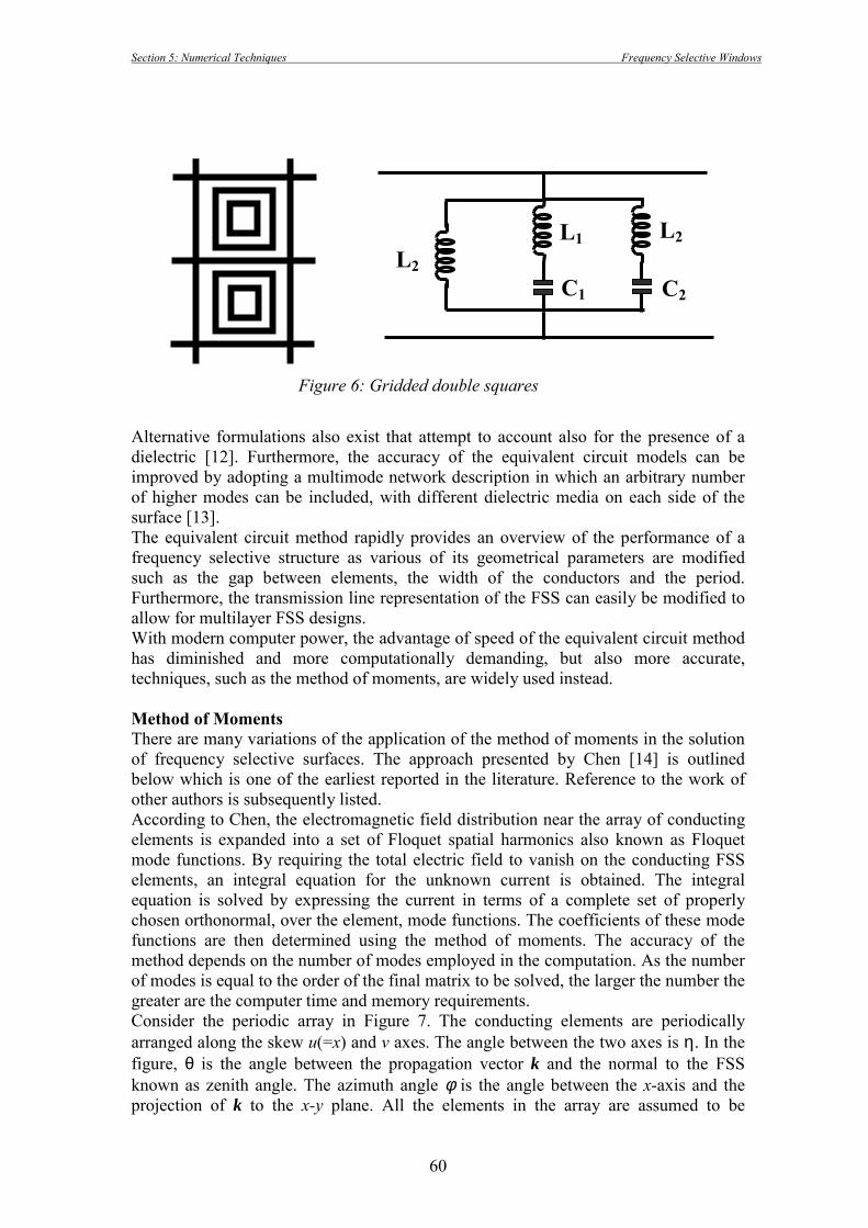
Section 5: Numerical Techniques Frequency Selective Windows
60
Alternative formulations also exist that attempt to account also for the presence of adielectric [12]. Furthermore, the accuracy of the equivalent circuit models can beimproved by adopting a multimode network description in which an arbitrary numberof higher modes can be included, with different dielectric media on each side of thesurface [13].The equivalent circuit method rapidly provides an overview of the performance of afrequency selective structure as various of its geometrical parameters are modifiedsuch as the gap between elements, the width of the conductors and the period.Furthermore, the transmission line representation of the FSS can easily be modified toallow for multilayer FSS designs.With modern computer power, the advantage of speed of the equivalent circuit methodhas diminished and more computationally demanding, but also more accurate,techniques, such as the method of moments, are widely used instead.
Method of MomentsThere are many variations of the application of the method of moments in the solutionof frequency selective surfaces. The approach presented by Chen [14] is outlinedbelow which is one of the earliest reported in the literature. Reference to the work ofother authors is subsequently listed.According to Chen, the electromagnetic field distribution near the array of conductingelements is expanded into a set of Floquet spatial harmonics also known as Floquetmode functions. By requiring the total electric field to vanish on the conducting FSSelements, an integral equation for the unknown current is obtained. The integralequation is solved by expressing the current in terms of a complete set of properlychosen orthonormal, over the element, mode functions. The coefficients of these modefunctions are then determined using the method of moments. The accuracy of themethod depends on the number of modes employed in the computation. As the numberof modes is equal to the order of the final matrix to be solved, the larger the number thegreater are the computer time and memory requirements.Consider the periodic array in Figure 7. The conducting elements are periodicallyarranged along the skew u(=x) and v axes. The angle between the two axes is η. In thefigure, θ is the angle between the propagation vector k and the normal to the FSSknown as zenith angle. The azimuth angle φ is the angle between the x-axis and theprojection of k to the x-y plane. All the elements in the array are assumed to be
L2
L1 L2
C2C1
Figure 6: Gridded double squares

Section 5: Numerical Techniques Frequency Selective Windows
61
perfectly conducting, identical and infinitecimally thin. In addition, since the field isperiodic, i.e. it satisfies the periodicity requirements imposed by Floquet’s theorem, itstangential component to the x-y plane can be expanded into transverse electric (TE)and transverse magnetic (TM) Floquet spatial harmonics.
(a) (b)
Figure 7 Plane wave incidence on a periodic structure with non-orthogonal axes ofperiodicity: (a) top view; (b) side view.
For the tangential electric field, tE , the TE and TM Floquet modes are
( )TEfor mn
yxtmn
xmynemn R
DDk
kk jiE
−=ΦΦΦΦ (1)
( )TMfor mn
yxtmn
ynxmhmn R
DDk
kk jiE
+=ΦΦΦΦ (2)
222ynxmtmn kkk += (3)
220
2tmnrrzmn kkk −µε= (4)
)zjkexp()yjkexp()xjkexp(R zmnymnxmmn −−−= (5)
where m,n indicate the order of the Floquet harmonic and 0022
0 εµω=k . The signs inequation (5) are modified appropriately to allow for propagation along the positive ornegative Cartesian axis direction. The modal propagation constant zmnk must bepositive for propagating harmonics and negative imaginary for evanescent harmonics
220 tmnrrzmn kkk −= µε for 22
0 tmnrr kk >µε (6)
Plane wave projectionon u-v plane
φ ηx, u
vy
Dx
Dy
z
θx, u
incident planewave
Section 5: Numerical Techniques Frequency Selective Windows
62
220 tmnrrzmn kkjk −−= µε for 22
0 tmnrr kk <µε (7)
Furthermore,
x
incxxm D
mkk π+= 2 (8)
ηπ−π+= cotD
mD
nkkxy
incyymn
22 (9)
where Dx and Dy are given by,ux DD = (10)
ηsinvy DD = (11)
In addition, incy
incx k,k are the propagation constants of the incident plane wave along the
axes of periodicity,φθµε= cossin0 rr
incx kk (12)
φθµε= sinsin0 rrincy kk (13)
Where εr, µr represent the relative permittivity and permeability respectively of themedium in which the FSS elements are situated. In the case of Chen the medium wasfree space εr = µr = 1.The transverse electric and magnetic fields are related by the modal impedances,
mnz
rTEmn k
hµωµ0= (14)
r
mnzTMmn
kh
εωε0= (15)
Thus, the tangential field of the incident plane wave can be decomposed into TE andTM harmonics of order m = n = 0,
∑=
=2
10000
rrr
it A EE ΦΦΦΦ (16)
( )∑=
×=2
100
00
00
rr
r
rit h
AEkH ΦΦΦΦ (17)
where k is the unit vector in the positive z-direction and A00r is a measure of themagnitude of the incident plane wave. The subscript r = 1 or 2 indicates the TE andTM Floquet harmonics respectively.The tangential reflected field is also expressed in terms of Floquet harmonics,

Section 5: Numerical Techniques Frequency Selective Windows
63
∑∑∑=
+∞
−∞=
+∞
−∞=
=2
1rrmnrmn
nm
Rt Q EE ΦΦΦΦ (18)
( )∑∑∑=
+∞
−∞=
+∞
−∞=
×−=2
1rrmn
rmn
rmn
nm
Rt h
QEkH ΦΦΦΦ (19)
From the orthonormality property of the Floquet harmonics one may obtain thereflection coefficients of each of the propagating and evanescent harmonics as follows,
∫∫ •×=
elementconductive
*rmn
Rtrmnmnr dShQ EHk ΦΦΦΦ (20)
where ∗ indicates “the complex conjugate of”.Chen subsequently specifies the following boundary conditions on the conductingplates
0EE =+ Rt
it over each plate (21)
( ) KHHk =+× Rt
it2 over each plate (22)
K being the surface electric current.
By inserting equations (16), (18) and (20) in (21) the following equation is obtained,
∫∫∑∑∑∑ •×−==
+∞
−∞=
+∞
−∞==elementconductive
*rmn
Rt
rrmnrmn
nmrrr dShA EEE Hk ΦΦΦΦΦΦΦΦΦΦΦΦ
2
1
2
10000 (23)
To solve equation (23), Chen expressed the induced current RtHk ×− in terms of
another set of modal functions, lpqΨΨΨΨ , which are appropriate for the conductive FSSelement under consideration and satisfies the element’s boundary conditions. Thesemodal functions are also orthonormal and provide a faster convergence than theFloquet harmonic expression in equation (19). The subscripts p,q indicate the modeorder and the subscript l indicates the polarisation type TE or TM ( l= 1 or 2respectively). Thus,
∑∑∑=
+∞
=
+∞
=
=×−2
100 llmnlpq
qp
Rt B ΨΨΨΨHk (24)
In order to eliminate the magnetic field in equation (16) and obtain the matrix equationto be solved, both sides of equation (16) are multiplied by the complex conjugate of

Section 5: Numerical Techniques Frequency Selective Windows
64
LPQΨΨΨΨ . Both sides of the subsequent equation are integrated over the FSS element areaS. The following equation is therefore obtained,
∫∫∑∑∑∑ •×−==
+∞
−∞=
+∞
−∞==elementconductive
*rmn
Rt
r
PQL*mnrrmn
nmr
PQL*rr dSChCA EHk ΦΦΦΦ
2
1
2
10000 (25)
where
∫∫ •=
elementconductive
*rmnLPQ
PQLmnr dSC EΦΦΦΦΨΨΨΨ (26)
From equation (25) a matrix equation can be set up with the mode coefficients Bmnl asthe unknowns,
][]][[ PQLpqlpqlPQL
DB =Z (27)
where ][ pqlPQL
Z is a square impedance matrix. Its row index is designated by P,Q,L, and
the column index is designated by p,q,l. The matrix elements are
pqlmnr
r
PQL*mnrrmn
nm
pqlPQL CChZ ∑∑∑
=
+∞
−∞=
+∞
−∞=
=2
1
(28)
and
∑=
=2
1
*0000
r
PQLrrPQL CAD (29)
Hence, by solving the matrix, the unknowns Bmnl and subsequently the reflectedFloquet harmonics amplitudes and power can be obtained.Chen also suggests that the functions l
pqΨΨΨΨ , which are also known as entire domainbasis functions [17], are the dual functions for the transverse electric field functions forthe equivalent waveguide problem. He provides an example of a set of functions forthe rectangular patch based on the rectangular waveguide modal functions.The work of Chen was subsequently extended to allow for the calculation oftransmitted fields. Montgomery [15] showed how a dielectric substrate can beincorporated in the calculations. He also indicated that the coupling coefficients C inChen’s work can be evaluated in closed form. Entire domain basis functions for otherconducting elements are presented by Mittra, Chan and Cwik [17]. Subsectional(subdomain basis) current functions were subsequently introduced. The advantage, asRubin and Bertoni [16] indicate, is the ability to model conductive elements (orapertures) of arbitrary shape. The price paid is an increase in matrix size [17] withconsequent increase in computer memory and time requirements. The memoryrequirements can be minimised by using iterative methods of matrix solution(conjugate gradient method) [17]. A summary of techniques for analysing frequencyselective structures was published by Mittra, Chan and Cwik [17]. The spectral domainmethod is also considered in Wu [18], Scott [19] and Vardaxoglou [20]. An alternativeapproach to solution of FSS is presented by Munk [21].

Section 5: Numerical Techniques Frequency Selective Windows
65
References
[1] N. Marcuvitz, Waveguide Handbook, McGraw Hill, 1951.[2] J.R. Wait, “Reflection at arbitrary incidence from a parallel wire grid”, Applied Sci.Res., 1954, vol. 4, pp. 393-400.[3] R.J. Langley and E.A. Parker, “Equivalent circuit model for arrays of squareloops”, Electronics Letters, vol. 18, no. 7, 1982, pp. 294-296.[4] C.K. Lee, R.J. Langley, “Equivalent-circuit models for frequency-selective surfacesat oblique angles of incidence”, IEE Proceedings Pt. H, vol. 132, no. 6, 1985, pp. 395-399.[5] R.J. Langley and E.A. Parker, “Double-square frequency-selective surfaces andtheir equivalent circuit”, Electronics Letters, vol. 19, no. 17, 1983, pp. 675-677.[6] C.K. Lee and R.J. Langley, “Design of single layer frequency-selective surface”,International Journal of Electronics, vol. 63, no. 3, 1987, pp. 291-296.[7] R.J. Langley and C.K. Lee, “Design of single-layer frequency selective surfaces formultiband reflector antennas”, Electromagnetics, vol. 5, no. 4, 1985, pp. 331-347.[8] I. Andersen, “On the theory of self-resonant grids”, The Bell System TechnicalJournal, vol. 54, no. 10, 1975, pp. 1725-1731.[9] R.J. Langley and A.J. Drinkwater, “Improved empirical model for the Jerusalemcross”, IEE Proceedings Part H, vol. 129, no. 1, 1982, pp. 1-6.[10] J.A. Arnaud and J.T. Ruscio, “Resonant-grid quasioptical diplexer”, ElectronicsLetters, vol. 9, no. 25, 1973, pp. 589-590.[11] J.A. Arnaud and F.A. Pelow, “Resonant-grid quasi-optical diplexers”, The BellSystem Technical Journal, vol. 54, no. 2, 1975, pp. 263-283.[12] S.W. Lee, G. Zarrillo, C.L. Law, “Simple formulas for transmission throughperiodic metal grids or plates”, IEEE Transactions on Antennas and Propagation, vol.30, no. 5, 1982, pp. 904-909.[13] A.N.A. El-Sheikh and R.J. Langley, “Multiport network analaysis f frequency-selective surfaces”, IEE Proceedings on Microwave Antennas and Propagation, vol.141, no. 3, 1994, pp. 229-231.[14] C.C. Chen, “Scattering by a two-dimensional periodic array of conducting plates”,IEEE Transactions on Antennas and Propagation, vol. 18, no.5, 1970, pp. 660-665.[15] J.P Montgomery, “Scattering by an infinite periodic array of thin conductors on adielectric sheet”, vol. 23, no. 1, 1975, pp. 70-75.[16] B.J. Rubin and H.L Bertoni, “Reflection from a periodically perforated planeusing a subsectional current approximation”, IEEE Transactions on Antennas andPropagation, vol. 31, no. 6, 1983, pp. 829-836.[17] R. Mittra, C.H. Chan and T. Cwik, “Techniques for analyzing frequency selectivesurfaces – a review”, Proceedings of the IEEE, vol. 76, no. 12, 1988, pp. 1593-1614.[18] T.K. Wu, Frequency selective surface and grid array, Wiley, 1995.[19] C. Scot, The spectral domain method, Artech House, 1989.[20] J.C. Vardaxoglou, Frequency Selective Surfaces – Analysis and Design, RSP,1997.[21] B.A. Munk, Frequency Selective Surfaces - Theory andDesign, Wiley, 2000.

Section 6: Conductive Paints and Opaque FSS fabrication Frequency Selective Windows
66
Section 6: Opaque Conductor FSS.
Conductive paintsConductive paints come under the term thick film laminates and are composed of amedium such as resin or more recently water, with a pigment of metallic particles.They have many properties such as particle size and shape, amorphous structure,porosity, layout properties in medium vehicles, percentage of conducting materialloading, particle compaction and dispersion additives. All these properties have aneffect on its electrical properties.
The electron flow from one pigment particle to another within the paint is determinedby such properties as the resistance of the particle pigment, the construction ofparticle chains within the holding medium and the inter particle gaps that form afterapplying the coating.
Typical conductive additives are made from solid spherical glass beads coated withsilver between 10 and 100 microns in size. The amount of silver coating can also beadjusted, typically between 4% and 33% by weight. Other metals such as copper andaluminum are used as well as different pigment shapes such as flakes and powders.These conductive pigments are used in a wealth of EMI/RFI shield products includingadhesives and sealants.
The effects of paint conductivity are determined by the degree of pigment loadingwithin the medium, how compact the pigment particles are within the medium, theuniformity of particle size and particle to particles contact. The typical pigmentloading levels for conductive paint are above 65%, below this conduction will notoccur and above this there is no great improvement although at higher levels theapplication can be thinner. Manufacturing processes are not the only parameters thataffect conductivity, environmental conditions such as heat and humidity stability,oxidation of the metallic particles and general wear and tear can also be important.
Substantial progress has been made in the last few years in developing resin systems,which are not only mechanically compatible with the substrate materials, but whichalso exhibit vastly improved shielding characteristics. It was not long ago that theprime complaint against makers of paint coatings was that the slightest abrasion orflexing of a plastic substrate resulted in conductive coating flaking off.
Twenty years ago conductive paints consisted mainly of nickel as the pigment, andwere dispensed by spray or brush. With the introduction EMI/RFI regulationsconsiderable interest has evolved in using other metal pigments and modern dispersaltechniques. This technology is evolving rapidly and with current developments theconductivity at lower applied thickness has continued to improve. Consequently thecost of coatings has continually reduced in cost.
With this increase in usage, the price of silver loaded paints has fallen significantly inrecent years and many products such as mobile phones are shielded using thisproduct. Hybrid blends such as silvered copper pigments will offer the highconductivity of traditional silvered paints at lower thickness. New technologies arelikely to produce water-based products that will reduce the hazardous materials thatare currently used in thinners and screen wash products. Development of short steel

Section 6: Conductive Paints and Opaque FSS fabrication Frequency Selective Windows
67
fibre paints will produce comparable conductive products without the use of preciousmetals and will consequently reduce cost.Three main metals are used in conductive coatings, with each one having a differentperformance characteristic (Table 1). Silver is a highly conductive metal impartingexcellent corrosion resistance. While cost is high, EMI/RFI shielding attenuation canrange between 50-75dB at most frequencies and surface resistivity comes down to0.01 ohms/ . Silver coatings are frequently specified for military applications whereelectromagnetic pulse protection (EMP) is required. For example, a 0.030mm dry filmthickness of silver will provide the same or better protection than a 0.225mm dry filmthickness of copper coating.
Copper has nearly the same electrical conductivity as silver, but at a lower cost. Onlyrecently has it been possible to provide a stable copper-based paint, by providing aspecial treatment to the copper flake filler to overcome its oxidation. Currentconductive acrylic paints consist of a water-based acrylic/urethane polymer and asilver plated copper filler. These offer electrical conductivity of 20 to 30 mΩ/ at athickness of 50 microns. They also offer high levels of abrasion and environmentalresistance.
Nickel has also been the subject of recent development work. Although not quite asgood a conductor as copper or silver, it absorbs more electromagnetic radiation onaccount of its magnetic permeability. The majority of nickel coated systems are air-drying and are applied with conventional spray equipment at a dry film thickness ofbetween 0.025mm and 0.05mm. This will yield greater than 40dB across a frequencyrange of between 5 MHz and 1.8 GHz and a surface resistivity of less than 10 ohms/ .Nickel conductive paints offer a most economic shielding for the majority of plastics.There is little or no surface preparation requirement and the spray application allowsfor high-speed production, resulting in low labour costs. Enclosures and cabinets withcomplex geometries can be coated without fear of incomplete coverage.
The main nickel systems for use on plastics are based on acrylic or polyurethane. Onefactor in the selection of the paint is the degree to which it can chemically attack andpermanently bond itself to the substrate, such that it cannot be readily abraded.
Silver 1.05 Nickel 0.20Copper 1.00 Iron 0.17Gold 0.70 Tin 0.15
Aluminum 0.61 Steel 0.10Magnesium 0.38 Lead 0.08
Zinc 0.29 Stainless Steel 0.02Brass 0.26
Table 1. Relative conductivity of metals
Improvements in wear and abrasion properties have made silkscreen printing ofconductive paints popular today in the manufacture of car windscreen de-foggers andprinted circuit board production particularly when surface mount technology is used.Carbon based paints are silkscreen printed directly onto printed circuit boards in theuse of membrane switch contacts.

Section 6: Conductive Paints and Opaque FSS fabrication Frequency Selective Windows
68
The manufactures of frequency selective surfaces are ideally suited towards silkscreen techniques deposited on different types of substrate etc.
The chosen material for pattern prototyping was a high performance conductive silverink (XZ250) supplied by Coates Circuit Products. This is screen printable ink usedtypically in the manufacture of membrane switches and flexible circuits and is capableof being printed on a variety of substrates. This ink is suitable for automatic andsemiautomatic printing machines and where quick drying is required. Typicalproperties are shown in the following table:
This ink is suitable for application onto a wide variety of substrates, includinguntreated and treated polyesters, which are commonly used for membrane switchassembly. Treated polyester is particularly recommended to ensure good adhesion ofsubsequent inks such as UV dielectrics and graphics inks.It can also be used on other substrates such as polymide, PVC, ABS rigid PCBsubstrates (phenolic and epoxy), glass and card etc. Compatibility tests of thesubstrate should be undertaken before print runs are carried out. Successful printingonto float glass and acetate film was undertaken for the prototype structures.
Conductivity is governed to a large extent by film weight. Therefore the mesh shouldbe selected to give the best combination of conductivity and economy.Mono-filament polyester meshes of 49 – 90T/cm. (125 – 230T/inch) can be used withmost types of photographic stencil. Thread pitch is a compromise between the filmconductivity and structure resolution, a mesh of 62T/cm provided adequate resolutionand conductivity for the prototypes. The paint is manually applied using mediumhardness squeegees.The table below shows typical surface resistivity values obtained with differentpolyester screens. In order to ensure a sufficient conductivity of the deposited paint, atechnique whereby the screen is placed slightly removed from the substrate giving animprovement in the film thickness.
All prints were dried as soon as possible after deposition in a fan convection oven,ideally at 120ºC (248ºF) for 30 minutes. Adequate drying is critical in achievingoptimum conductivity. Drying at higher temperatures or for longer times will reducesurface resistivity. The conductivity of the film can be significantly degraded if it isnot cured suitably after application.
Pigment SilverMedium Thermoplastic ResinViscosity 30 – 50 Poise 25°C (77°F)Solids 70%Specific Gravity 2.000Shelf Life 6 months sealed containerSheet Resistance <0.04Ω/ @ 15µm (0.6mil) dry film thicknessPencil Hardness 3H – 4HTheoretical Coverage 9m²/kg @ 0.015mm dry film thickness

Section 6: Conductive Paints and Opaque FSS fabrication Frequency Selective Windows
69
Mesh Count (TPC/TPI ) 49/125 62/120 77/195 90/230Surface Resistivity (mΩ/ )
As printed 32 22 39 50Normalized to 0.015mm dft 32 39 36 30
Dry film thickness (mm) 0.015 0.0027 0.014 0.009
Many applications use the ink as supplied, but where a reduction in viscosity isrequired thinners may be added to a maximum of 5% may be added. The final surfaceresistivity depends on the dry film weight, addition of thinners will increase this, andthus the use of thinners was avoided.Conductivity of pure metals may not always relate to shielding effectiveness. Thesurface of the metal, if exposed to air, may be chemically oxidised. Conductivity ofthe metal oxide would then be a better indication of shield effectiveness. For example,pure copper has excellent conductivity, but its oxide exhibits relatively poorconductivity. Therefore, any shielding system that uses copper must protect its surfaceagainst oxidation. The use of a thin coat that acts as an oxidation barrier is the mostcommon method of protection.
References:
[1] Dr. Yasin Zaka, “ Overview of Techniques for Applying Conductive Coatings toPlastics for EMI/RFI Shielding.” International Conference, Conductive Coatingsand Compounds. 21-22 June 1999. Brussels.
[2] Dr. Claudio PAGELLO, “Test Methods for EMC Coatings PerformanceAssessment.” International Conference, Conductive Coatings and Compounds.21-22 June 1999 Brussels.
[3] GE Plastics, Product Assembly Guide, Coatings/Shielding. Designing forElectromagnetic Compatibility.
[4] Coates Circuit Products. Technical Information. “ XZ250 High ConductivitySilver Touchkey Ink”, December 1996. T039/0. Coates Electrographics Ltd,Norton Hill, Modsomer Norton, Bath, Avon BA3 4RT.www.coates.com/electro/circuits/home.html
[5] T.K. Wu, “Frequency Selective Surface and Grid Array” John Wiley & Sons Inc.1995. ISBN 0-471-31189-8
[6] Chapter 6, Gregory S. Hickey, “Frequency Selective Surface Materials andFabrication”.
[7] Lt-Col. J.W. Molyneux-Child, “Comparing Metals for Conductive Coatings”Surrey Electro-Shielding Ltd.www.industrialtechnology.co.uk/surrey.html
[8] Chromerics Europe.

Section 6: Conductive Paints and Opaque FSS fabrication Frequency Selective Windows
70
Parker Hannifin PLC., Parkway, Bucks, SL7 1YB.Tel: +44(0) 1628 404000 Fax: +44(0) 1628 404890www.chromerics.com
[9] Potters BallotiniBury St. Edmunds. UK.Tel: +44(0) 1284 715400www.pottersbeads.com
Fabrication OverviewThe accurate modelling of frequency selective surfaces is a costly process in time andcomputer resources. In order to assess a structure’s full performance it is often lessexpensive and quicker to fabricate the structure and electrically measure itsparameters.The fabrication process usually initially needs a mask, which supplies the patterninformation for etching or depositing conductive materials and is usually written ingraphical language with the following prerequisites
1. Efficiently reproduce repetitive patterns at the required resolution.2. Identical output regardless of the computing platform, and output plotting device.
The interpreted Postscript ™ language or its GPL equivalent Ghostscript meet theabove requirements. This is a popular stack orientated language and has sufficientinherent mathematical functions to produce repetitive geometrical output on variouspage sizes. Dedicated Postscript printers or Ghostscript drivers for current printersenable plotting output to be easily obtained. Source files are written in ASCII formatand can be created or edited using many text editors. Commercial photographiclithography equipment supports the language, and thus professional output onphotographic film is easily obtained.
Adhesives play an important part in bonding the conductive layer to required substrateand fall into two categories, wet and dry.Dry adhesives take the form of a laminar structure, adhesive on both sides of thematerial and give a dry bond between the required layers. Such an example is Mactac,which is optically transparent.Wet adhesives, are obviously liquid in nature and are available in varying bondstrengths and viscosity. In the case of glass substrates, specialised ultra-violet curingmetal to glass adhesives such as Loctite 350. This adhesive leaves an opaqueappearance after etching.Careful attention needs to be made when bonding the conductive layer to the substratesuch that the bond is uniform and contains no deformations such as air bubbles, whichwill degrade the efficiency of the structure. Many structures are fabricated using anetching process, and the adhesive must be capable of withstanding the temperaturesand chemicals during this process.
Printing of conductive inks using the silkscreen process are common in surface mounttechnology, this can also be used to create structures of various sizes. Structures ofvarious sizes were fabricated by silk-screen printing onto acetate film and glass

Section 6: Conductive Paints and Opaque FSS fabrication Frequency Selective Windows
71
Figure 1
Figure 2
substrates. The silk screens are actually nylon and are re-useable, the printing patternis generated in similar way to pcb technology using ultra-violet sensitive materialsand techniques. Special screen washes applicable to the ink have to be used to cleanthe screens.
Fabrication MethodsThe following describes various fabrication techniques, each method was selected tomeet specific physical properties. The main objective is to produce a fss on a glasssubstrate.
Traditional Printed Circuit Board. (Figure 1)Copper laminated fibre-glass backed printed circuit board with an ultra-violetsensitive layer applied to the copper side is used. After exposure to ultra-violet lightthrough a pattern mask, It was developed and wet etched. Permitivity of the fibre-glass dielectric is not well documented for frequencies up to several GHz. Thismethod is used primarily to assess the properties of the geometric pattern within thestructure.
Copper on Glass substrate using wet adhesive. (Figure 2)Copper laminates have to be bonded individually if custom substrates are to beconsidered. This sample was made by using ‘Loctite 350’ adhesive to bond the copperlaminate to the glass, and then exposing the bond to ultra-violet light. The mainproblem is getting a uniform bond due to air bubbles forming between the layers, thismay be alleviated by using an adhesive with a lower viscosity. This technique is onlysuitable for transparent substrates. The copper is then sprayed with an ultra-violetsensitive lacquer and exposed via a mask to ultra-violet light. This is then developedand etched. The adhesive stands up well to the etching process, although there isdegradation around the edges.The adhesive also leaves an opaque appearance to the substrate after etching.

Section 6: Conductive Paints and Opaque FSS fabrication Frequency Selective Windows
72
Figure 3
Figure 4
Copper on Glass substrate using dry adhesive. (Figure 3)A dry adhesive (Mactac Permatrans) which is transparent is used to adhere the copperlaminate to the glass. Care during this process is again needed to eliminate all airbubbles, this being easier to achieve than wet adhesive. The same etching process as
Figure 3 was used, the adhesive withstood the temperature and etching process wellalthough degradation was found at the edges. The result produced a more transparentsubstrate than Figure 2 and had a more uniform laminate structure.
Copper on dry adhesive. (Figure 4)To test a particular structure on different substrates, the copper is bonded to the dryadhesive only, the protective backing on the reverse side left on. The etchingprocedure again was that of Figure 2. The resulting structure was uniform with a smalldegradation in the adhesive around the edges. The protective backing of the opposingside to the copper could be removed and applied to a substrate of choice. Thestructure could also be carefully removed from the substrate and applied to a differentone, this can be repeated many times giving a quick flexible test of substratecharacteristics upon the structure.
Silver paint on Glass/Acetate Substrate. (Figure 5)With advent of highly conductive printing inks, silk screen printing methods usingsilver inks are assessed. A silk screen mask of the required properties is producedfrom the pattern mask, traditional silk screen printing methods are used to print thepattern through the screen onto the required substrate. Due to the ‘thickness’ of thepaint shims are needed between the mask and substrate during printing in order toreduce ‘flaring’ of the pattern. To obtain maximum conductivity, the structure shouldbe heat cured. This method produces multiple structuresquickly and sizes up to 3m².

Section 6: Conductive Paints and Opaque FSS fabrication Frequency Selective Windows
73
Figure 5
Figure 6
Silver paint on Acetate with dry adhesive. (Figure 6)In an attempt to obtain maximum testability of different lattices and substrates acombination of techniques from methods 3 and 4 are used. This structure is silk screenprinted onto acetate film and then backed by the dry adhesive. This gave maximumflexibility in that the structure could be adhered to differing substrates and theindividually pattern elements could be cut away and repositioned on a different lattice.Also structures could be placed on top of one another allowing the testing of multi-layer structures.
In performance testing of the above structures, it has been assumed that the variousadhesive and acetate films have no significant effect, this needs to be investigatedfurther. All the methods produced working frequency selective surfaces, by far themost versatile being method 6. New materials are being developed rapidly, such astransparent metals on film, these still have to be investigated. The most critical factorin creating a fss is using a material with suitable conductivity, if the conductivity ispoor it will not operate at high frequencies.
Material References
1. PCB Photo-Resist copper clad FR4 board.RS Components, PO Box 99, Corby, Northants, NN17 9RSTel: 01536 201201 Fax: 01536 201501http://rswwww.com
2. Domestic Float GlassPope & Parr, 118/120 Talbot St., Nottingham, NG1 5HH.Tel: 0115 9473015, Fax: 0115 9473015.

Section 6: Conductive Paints and Opaque FSS fabrication Frequency Selective Windows
74
3. PRP 200 Positive PhotoresistElectrolube, Wentworth House, Blakes Rd., Wargrave, Berkshire. RG10 8AW.Tel: +44 (0) 1189 404031. Fax: +44(0) 1189 403084.www.electrolube.com
4. Loctite 350 (35038) UV Curing Adehesive glass/metal.Henkel Loctite Adhesives Ltd., Watchmead, Welwyn Garden City, Hertfordshire,AL7 1JB.Tel: +44(0) 1707 358800. Fax: +44(0) 1707 358900.www.loctite-europe.com
5. Mactac Permatrans 2113 film adhesiveMactac UK Ltd., 4-6 The Britannia Trade Centre, RyeHill Close, Lodge Farm,Northampton, NN5 7UA.Tel: +44(0) 1604 756521 Fax: +44(0) 1604 758150www.mactac-europe.com
6. XZ250 High Conductivity Silver InkCoates Screen., Cray Avenue, St. Mary Cray, Orpington, Kent BR5 3TT.Tel: +44(0) 1689 875201. Fax: +44(0) 1689 878262
7. Copper Clad LaminateCrossley & Bradley Ltd.Ulneswalton Lane, Leyland, Preston, Lancs. PR26 8NB.Tel: +44(0) 1772 452236. Fax: +44(0) 1772 456859.

Section 7: Review Of Transparent And Conductive Oxides Frequency Selective Windows
75
Section 7: Review Of Transparent And Conductive Oxides
Introduction
Among the aims of this feasibility study is the investigation of the possibility ofreplacing the conductive metal in the FSS structures with equally conductive buttransparent material (TCO) for aesthetic as well as practical purposes. It is moreappealing to the eye if the total transparency of the window is not disturbed by theopaque nature of the most metals. On the other hand working conditions in spacesprotected by FSS structures might necessitate visual continuity through thesestructures.
The first semitransparent and electrically conductive CdO film was reported as earlyas 1907. However substantial technological advances were only made after the 1940swhen interest on these materials was generated by their potential applications inindustry. Such films have been used as transparent electrical heaters for windscreens,as gas sensors, in solar cells, heat reflectors, protective coatings, light transparentelectrodes, laser resistant coatings, anti-static surface layers in satellites, surface layersin electroluminescent devices, and recently in horticultular glasshouses.Such transparent conductive materials are mainly oxides of indium, zinc, cadmium,tin, and combinations between these oxides.Thin films of metals (gold, silver, copper, iron ) have also been found to have similarproperties but in general are not very stable and their properties change with time.They are also inferior to the former in terms of hardness and transparency.The basic properties of these films that are most important for practical applicationsare their structure, morphology, electrical conductivity and optical transparency.These properties can be altered selectively by introducing different dopants and alsoby using different growth techniques.Ideally both optical transmission and electrical conductivity should be as large aspossible. However the simultaneous accomplishment of both high transmission andconduction is not possible since these parameters are inversely proportional. Youcannot have optimum conductivity without sacrificing transparency.In this report we will summarize the findings of different research groups according totheir electrical and optical properties after we have introduced the different growthtechniques with their corresponding merits.Immediately after the introduction of each technique a section follows with thesummary of the different experimental results that have been presented in theliterature.A number of different deposition techniques have been used to deposit TCOs. Sincethe electrical and optical properties of these films depend strongly on theirmicrostructure, stoichiometry, and the nature of the impurities present during growth,each technique yields films with different behavior. This is also particularly true whenthe same technique is used by different research groups, since identical arrangementof the growth systems in conjunction also with the growth parameters is the exceptionrather than the rule.The main TCOs that we shall discuss are tin oxide (SnO2), indium oxide (In2O3),indium tin oxide (ITO), and zinc oxide ZnO).If these semiconductors are prepared intrinsically i.e. without intrinsic or extrinsicdopants their resistivity is very high (of the order of ≥107 Ω cm). The low resistivitythat is required for their application as TCOs can be achieved in two ways:

Section 7: Review Of Transparent And Conductive Oxides Frequency Selective Windows
76
♦ Creation of intrinsic dopants by lattice defects. These can be oxygen vacancies ormetal atoms on respective lattice sites, and with
♦ Introduction of extrinsic dopants (atoms of materials foreign to the pure form ofthe original compound). These can be either metals with one additionalconduction electron on zinc lattice sites or halogens with one additional electronon oxygen lattice sites.
Among them the most popular are the ITO and the ZnO. The ZnO based TCOs arefavoured over to ITO due to the lower production cost, lower toxicity and greaterstability in atmospheric environment.
Growth techniques
The growth technique plays a significant role in controlling the properties of thesefilms because the same material deposited by two different techniques usually hasdifferent physical properties.This is due to the fact that the electrical and optical properties of these films stronglydepend on the structure and morphology of the film, and on the nature of theincorporated impurities. These properties are depended in turn on the variousdeposition parameters used which when properly chosen can produce films with thedesirable characteristics.In these section we will discuss numerous deposition techniques that have beenemployed to grow transparent conductive oxide films (TCOs).
Chemical vapour deposition (CVD).
This technique is widely used in the semiconductor industry for its capability toproduce high quality thin films without the need for high vacuum. This techniqueinvolves the reaction of one or more gaseous species on the surface of the substrate.A vapour containing the condensate material is transported to the substrate surfacewhere it is decomposed.A thin film is deposited as a result on the substrate. For TCOs usually volatileorganometallic compounds are used. A carrier gas such as oxygen, water, argon ornitrogen carries the vapours of these compounds. The decomposition process shouldbe such that the reaction occurs only at the substrate surface and not in the gaseousphase. The quality of the films depends on various parameters, such as substratetemperature, gas flow rate and system geometry. In order to obtain the best qualityfilms these parameters should be optimized.Particularly for TCOs if the substrate temperature is low, carbon occlusions are foundin the films because of the incomplete oxidation of the organic material. However, ifthe substrate temperature is too high it will result in the decomposition of theorganometallic compounds in the gas phase rather than the substrate, therebyproducing powder-like deposits instead of a smooth film.The main advantages of CVD are the simplicity, reproducibility and large-scaleproduction capability without the need for high vacuum as an essential requirementfor deposition. Moreover, due to the low cost of the equipment used, the cost ofproduction is low. Unfortunately the nature of the chemical reaction demands highdeposition temperatures, in excess of 450°C.

Section 7: Review Of Transparent And Conductive Oxides Frequency Selective Windows
77
In some variations of the main method the creation of a plasma around the substrateresults in better quality films at lower deposition temperature. This is called plasmaassisted CVD.The gasses that are generally used are very toxic to humans and extremely flammable,needing special handling requirements. Most of them are not harmful to ozone layer,though. This information was provided by EPICHEM (contact Mr Colin Overton, Tel:01513342774)
Atomic layer epitaxy
Like CVD atomic layer epitaxy (ALE) is an epitaxial chemical vapour processproducing, like all epitaxial processes, good quality films. ALE relies on the self-limiting reactions between alternately dosed gaseous precursors, and is capable ofproducing films with uniformity and excellent thickness control even on complexsurfaces. At first, the precursor of the first atomic constituent atom of the film to bedeposited, is flushed into the high vacuum chamber where it breaks down at thesurface of the substrate depositing a thin layer of a few atomic distances in thicknessof the first constituent. A rapid cycle of purging with inert gas follows to clear anyremains of the first gas, followed by the next flushing of the precursor of the secondconstituent. Again the same process leaves an atomic layer of this constituent whichnow reacts with the previous atoms to form well-ordered crystals. At the moment thismethod is used predominantly for the production of high quality electroluminescentdevices with II-VI phosphors. Due the slow growth rate it is not very cost efficient.
Experimental and comparative results
CVD has been extensively used for the production of tin oxide and with some successfor zinc oxide.For the former stannous and stannic chloride, tetramethyl tin, dimethyl tin dichlorideand dibutil tin diacetate are most commonly used. These gases are oxidised at hightemperatures by oxygen or water. When water is used lower deposition temperaturesare employed.Regarding indium oxide the cost of the relevant organometallic compounds isprohibitive, so the CVD method rarely has been used. When indium acetylacetonate isused, oxygen must be used for the oxidation. On the contrary two-ethylhexanoaate isused with inert nitrogen only.When indium and tin acetonates (In(C5H7O2)3 and Sn(C5H7O2)2) are used fordeposition of indium tin oxide low resistivities and high transparencies are achieved.For tin oxide, tetramethylin or TMT (Sn(CH3)4) is used with oxygen as reactants.Although TMT is flammable and toxic, it is stable in air and moisture and can besafely contained in a glass or quartz vessel.For zinc oxide deposition organometalic compounds are substituted by zinc vapour. Amixture of nitrogen with water or hydrogen is used to start the reaction. Whenammonia is used instead, better films are produced but at lower rate. Alternatively,Zn(C5H7O2)2 was used as a precursor for Zn and In(C5H7O2)2 was used as a precursorfor In. The carrier gas was nitrogen and the deposition temperature was 525 °C.It is reported in one very recent study that ZnO doped with Ga and In is moreconductive than when Al and In are used as dopants. In the same study it wascommented that CVD prepared ZnO is more stable in harsh atmospheric conditionsthan the sputterd ZnO.

Section 7: Review Of Transparent And Conductive Oxides Frequency Selective Windows
78
Generally there are not many publications for CVD deposited TCOs in comparisonwith sputtered and evaporated ones.Regarding ALE research have been carried on since 1994 mainly by the University ofHelsinki where the process first originated. InCl3 and SnCl3 are the precursors forIndium (In) and tin (Sn) respectively. H2O or H2O2 are used to initiate the chemicalreaction. There are many publications were the process is explained and differentdesigns are proposed.
The following table summarizes the above comments:TABLE 1TCO Substrate
Temperature°°°°C
RateA/min
ResistivityΩ cm
Transmission %
Remarks Ref.
SnO2 250-400 ------ 10-10-3 80-95 SnCl4+H2O 50
SnO2 480-680 ------ 4x10⁻²-10-3 90 ------ 2
SnO2 420 ------ 5x10⁻³ 90 O2+H2O 3
SnO2:P 400 ------ 7.5x10⁻⁴ 83 ------ 4
SnO2:F 570 3600 3.3x10⁻⁴ 90 ------ 5
In2O3 527 7980 9.3x10⁻⁴ 89 ------ 6
ZnO:Al 367-444 ------ 3x10⁻⁴ 85 ------ 7
ZnO:Ga ------ ------ 1.2x10⁻⁴ 85 Very stable 8
ZnO:In ------ ------ 1.1x10⁻⁴ 85 Very stable 9
ZnO:In 525 ------ 4.6x10⁻³ 90 ------ 10
ITO 450 ------ 1.8x10⁻⁴ 90 Sn/In=0.031
11
ITO 300-500 6.5 3.9x10⁻⁴ ------ ALE 242
Vacuum evaporation.
Vacuum evaporation is one of the oldest and most widely used methods for depositingthin films. The Joule conductive heating of metal wires which in the form, generally,of baskets or boats are used to house the source material, is employed to decomposethis material into different chemical constituents (thermal or flash evaporation). Thesethen are deposited to form thin films on the opposite situated substrate.An appropriate heater can heat the substrate if it is so required. The evaporation canbe carried out in vacuum or in the reduced environment of a selected gas. For TCOevaporation, oxygen or an argon-oxygen mixture is usually used. The importantcontrol parameters are the substrate temperature, evaporation rate, source-to-substratedistance and oxygen partial pressure. The TCOs can be evaporated in three ways: (i)by directly evaporating metal oxides, (ii) by reactive evaporation of the metal in thepresence of oxygen, or (iii) post-oxidation of metal films. It is common to heat-treatthe grown films at high temperatures in water, hydrogen or oxygen environment toimprove further the conductivity.

Section 7: Review Of Transparent And Conductive Oxides Frequency Selective Windows
79
As in CVD different versions of evaporation exist to facilitate the reaction betweenthe evaporants and the gas, such as in a plasma or in a low power laser source shiningat the substrate so chemical reactions can be promoted further.The vacuum thermal evaporation is a cost- effective method with high depositionrates (R), albeit suitable only for small substrates. The deposition temperature is alsohigh enough for this method to be prohibitive for glass substrates. The possibility ofintroducing impurities from the material of the crucible is also high.
Electron beam evaporation
This method is another form of evaporation where a beam of electrons is used tovaporize the material of the target. It is more controlled and cleaner than thermalevaporation with the result of producing higher quality films. It is also suitable formany materials. A continuous source of electrons can be used to vaporize a materiallocally. It can be used for deposition on large substrates and so, it is suitable forindustrial applications. Contrary to the sputtered or ion plated films were ionbombardment can cause damage to the growing film, e-beam evaporated films aremore crystalline (they have larger grain size and lower defect density). Usually due tothe high quality of these films, lower substrate temperature is used without thenecessity of post-deposition annealing.There are variants of this technique as well.By creating an arc between the cathode and anode the deposition rate increasesdramatically (usually it is between 6-20nm/sec).There are different types of arcs depending on the manner that are created at theelectrodes. Glow cathode, cold cathode as well as hollow cathode variations can beused.This method is very sensitive to the presence of water vapor in the system, and thefilms show poor quality when this occurs.Alternatively by introducing an ion source where the ions are bombarding thesubstrate during growth, denser and more adhesive films are created, even at roomtemperature without any post-deposition annealing. These ions can be monomeroxygen ions or clusters of oxygen ions with mean size of 3000 atoms per ion or evenargon ions. Their size of course can vary to suit different applications. Cluster ionsdue to their size interact only with the surface of the growing film resulting insmoother, cleaner and well ordered films. The deposition temperature can be low aswell. Changes in the angle of incidence of the ions to the substrate have been found tobe important in tailoring the properties of the films.We can say that ion assisted evaporation results in improved film properties, likeincreased adhesion, hardness, and packing density compared to sole e-beamevaporation. More on the subject of ion-assisted deposition will be discussed in thesection dedicated to ion deposition processes later on.Recently, a process where the deposition is achieved by e-beam evaporation at veryslow rate and a temperature gradient is present across the substrate has resulted in thelowest resistivity in ITO ever reported (4.4x10⁻⁵ Ω cm). The slow rate allowsdeposited atoms to diffuse and be positioned favourably on the substrate, where as thetemperature gradient promotes the formation of crystalline grains with similarorientations at neighbouring sites. This method is called zone-confinement.

Section 7: Review Of Transparent And Conductive Oxides Frequency Selective Windows
80
Usually the deposited ITO film is formed in a mixture of hexagonal and cubiccrystalline grains. This is an arrangement that can create scattering in the movingelectrons when crossing through neighbouring grains due to very defective boundarythat separates them. This causes reduction in mobility and thus lowers theconductivity.In any deposition process the first atoms that arrive at the clear substrate surfacesegregate at distinct places called islands of formation and form crystallites if thetemperature of deposition is high enough. Otherwise these islands are made fromamorphous material. These crystallites eventually grow and merge into each other toform a film. In non-epitaxial processes, like the ones we are discussing here, thesecrystallites contain material in different orientations called grains. When there is atemperature gradient between two crystallites the defects that have been formed, ordopant atoms that have not been integrated are pushed to the boundaries (this isespecially true for ITO). The result is that grains within a zone (i.e. crystallites thathappen to grow at almost uniform temperature) are oriented in the same direction andthe boundaries that separates them are twin boundaries that cause little scattering inthe moving electrons. So higher conductivity is achieved due to increased mobilityalong certain planes.
Experimental and comparative results
A wide range of vacuum evaporation techniques has been used to deposit tin oxidefilms. Flash evaporation [13] has been nowadays substituted by e-beam evaporation[14,15] for the reasons we stated above. Tin can be used as target in oxygenatmosphere or instead a tin oxide target can be employed in vacuum. The as-evaporated films mainly have SnO phase (which is semi-transparent), and is producedby decomposition of SnO2 molecules during evaporation. Post-deposition is generallynecessary in order to obtain transparent conducting oxides. If the films are amorphouspost deposition is carried out in the presence of oxygen. The angle of incidence ofSnO2 vapour onto the substrate significantly affects the growth behaviour of thesefilms [16,15]. Films grown at incidence angles less than 60° are highly resistive andyellowish brown in colour and rich in SnO phase. Heat treatment must follow to turnthe films that are opaque into transparent.In a recent study arc discharge vapour deposition was used for tin oxide. Parallel tothe deposition an electrical current was applied with two electrodes on the substrate.The electric field is possibly causing intensified electromigration along highresistance paths. SEM data show that the imposition of an electric field parallel to thesubstrate causes a modified microstructure to form. This growth might be aided byintensified electromigration or by a thermodynamically favoured condition by thepresence of the field.Vacuum evaporation is more commonly used for indium oxide than tin oxide [20-26].Again the same general remarks that have been stated above are true. However, it wasobserved that incorporation of metallic indium in the evaporation source not onlysignificantly enhanced the rate of evaporation, but also significantly improved theoptical and electrical properties of the films.In one study [19,20] it was found that films grown with tantalum (Ta) or tungsten (W)heater had the worst conductivity. It was suggested that a chemical might had beentaken place between the indium and these metals. As a remedy a proper combinationof crucible and a heater element or a crucible with a high lip might be used instead.

Section 7: Review Of Transparent And Conductive Oxides Frequency Selective Windows
81
A plasma can be used close to the substrate to enhance the reactivity of In vapour withoxygen so as lower temperature can be used [21,26]. A tungsten (W) emitter and avoltage supply can create the plasma.There are many reports on the deposition of ITO by evaporation as well [27-36]. Mostresearchers have deposited these films by reactively evaporating either metallic alloyor an oxide mixture. Some times two metallic sources are used. Sequential metallicevaporation of In and Sn is used as well, followed by annealing [28,41]. Theadvantage of this method is that the composition of the films can be controlledaccurately. The substrate temperature has to be more than the crystallizationtemperature of ITO which is 150°C in order to avoid deposition of amorphous films[37]. However, it has been argued that the deposition rate is more important than thesubstrate temperature in producing transparent films [38]. Although very highdeposition rate results in worse conductivity and transparency, and increase in thedeposition temperature can not offset this effect. In this study the deposition rate wasvaried from 2-120 A/min [38].The method of applying an electric field parallel to the substrate during growth hasalso been tested on ITO deposition [43]. The DC electric field was varied between 0-110 Volts. However, the resistance of the films was high, being between 100-108Ω.No other parameters were given to deduct the resistivity. The high resistance might beexplained by the poor vacuum conditions.Below follows a table that summarises the most significant results that have beenreported in the literature concerning the evaporation deposition of some of the TCOs.
TABLE 2TCO Substrate
TemperatureC°°°°
RateA/min
ResistivityΩΩΩΩcm
Transmission%
Remarks Ref.
SnO2 480 60-120 0.03-40 >85 In O2 17SnO2:Mo 480 60-120 3x10⁻³ >85 In O2 17SnO2 RT ------ 5x10⁻⁴ ------ Arc+cur 18In2O3 320-350 ------ 1.8x10⁻⁴ >95 Flush+O 19In2O3 350 or 200 ------ 3.2x10⁻⁴ >96 Flush ,Ar+O 21,26ITO 400 ------ 2x10⁻⁴ 80 Flush+O 44ITO 350 400 8.8x10⁻⁴ 88 Plasma
flush+O26
ITO ------ ------ 4x10⁻³ >90 Sequential+O
28
ITO 200 96 2.4x10⁻⁴ 90 e-beam+O 29ITO ------ 4000 1.7x10⁻⁴ 80 e-beam,large
areaapplications
45
ZnO 150-200 ------ 1.5x10⁻³ 89 Flush+O 46
Sputtering
Sputtering is one of the most versatile techniques used for the deposition oftransparent conductors when high quality films are required. It is widely used indifferent versions and modifications. Recently, a highly conductive and transparentITO was produced in the opto-electronics lab of Nottingham Trent University, whichcompetes favourably worldwide with the best reported ITO [47]. Additionally,

Section 7: Review Of Transparent And Conductive Oxides Frequency Selective Windows
82
literature survey done in order to complete the current report revealed the wide extentof the use of sputtering in research labs and industries around the world.So, there are enough reasons to cover in detail this versatile technique. However, wewill concentrate only on these variations of the main technique that have been usedsuccessfully in developing good quality TCOs.Compared with other techniques, sputtering produces films with higher purity andbetter-controlled composition. It provides films with greater adhesive strength andhomogeneity and permits better control of film thickness [48]. Many differentmethods are categorized as sputtering because they have in common the ionization ofa material by generation of a plasma, which is in close confinement and next to asubstrate where deposition subsequently occurs.The sputtering process involves the creation of a gas plasma (usually it is an inert gassuch as argon) by applying a voltage between an anode and a cathode. The cathode isused as a target holder and the anode is used as a substrate holder. The voltagepotential causes the dissociation of gas atoms into ions and free electrons. The ionsare attracted to the cathode where by momentum transfer, particles are ejected fromthe surface of the target and they diffuse away from it been deposited onto thesubstrate. When the kinetic energy of the ions exceeds the heat of sublimation (orchemical bond energy) of the target material (roughly by four times) sputteringhappens. The electrons are responsible for the sustenance of the plasma because thereare smaller and move quicker [49, 50]. By this reason they diffuse quickly and theybombard the substrate, thus increasing its temperature sometimes by a couple ofhundred of degrees Celsius. Across the plasma a negative potential forms, and overthe electrodes an even bigger negative potential drop exists due to thethermodynamics of the whole process. The difference between these two potentialsdetermines the energy of those ions, which strike the electrodes and the ejectedcharged species.The ions also diffuse and can cause problems. There can be positive and negative ionsin a plasma. Usually a source of the former is the inert gas and of the later the reactivegas. The sputtered material mostly exists in atomic form, and so it is neutral [51]. Acause of film degradation is the production usually of negative ions, also, duringsputtering of the target. This is especially true for oxide targets, where production ofnegative oxygen ions is frequent. These negative oxygen ions will suffer additionalacceleration due to their charge and re-sputter the substrate [52- 55]. Other researchdone on this topic failed to detect any negative ions, all the observed ions werepositive and existed either in elemental or compound form [56]. However, re-sputtering is a serious problem and causes degradation of the film.
The main merits of sputtering are:♦ Different materials can be sputtered at almost comparable deposition rates. This is
not true for evaporation where the same temperature can give widely ranginggrowth rates for different materials. So, with sputtering different materials can beco-deposited.
♦ One can sputter films of complicated materials, like stainless steel, pyrex,permalloy et al without composition changes between target and film.
♦ Film-thickness control becomes relatively simple.♦ Sputtering can be accomplished from large area targets.♦ In sputtering there are no difficulties with “spitting” or ejection of large
agglomerates instead of simple ions. This often occurs in vacuum evaporation.There are also no restrictions with substrate arrangement. So, often downward

Section 7: Review Of Transparent And Conductive Oxides Frequency Selective Windows
83
sputtering, where the target is positioned above the substrate is preferred. If thedischarge is operated at gas pressures lower than about 5mTorr, the sputteredatoms arrived at the substrate with high kinetic energy. This maybe beneficial tofilm structure and the adherence to the film.
The main disadvantage is the relatively low deposition rates.There are two methods of powering the sputtering system: by DC or by RF source.In a DC sputtering system a direct voltage is applied between the anode and thecathode. It takes a considerable voltage drop across the electrodes to start initially theplasma. The bombardment of the target by the gas ions not only ejects target materialspecies but also produces stray electrons, called secondary electrons [57]. Theseelectrons are responsible for sustaining the plasma, since in DC excitation electronrecombination with ions is frequent. In some cases the plasma can be excited orsustained by a hot thermionic cathod, which emits electrons to replace the lost ones, inorder to use less voltage across the electrodes.Stabilization of the plasma in DC excitation mode has been a challenging task formany years. Arching is among the factors that can destabilize the plasma. It happensmainly when insulating or compound materials are used as targets. During theprocess, thin dielectric layers grow in the non-eroding areas of the target whichsteadily charge up due to the bombardment of the positive ions. Arching then occurswhich generates particulates and contaminates the film. If arching will not terminatethe process, eventually after sputtering for a period, the walls and the anode would becovered with insulating material, which will disrupt the process [58]. So, DCsputtering is used mainly for conducting films such as metals like indium, tin or zincand leads to very high deposition rates. This is an advantage because metallic targetsare easier to manufacture with high purity, and are thermally conductive, so they donot crack easily. However, in this case higher quantities of oxygen must be present inthe system for reactive deposition to take place. This also causes reactions to takeplace at the surface of the metallic target transforming it into a compound insulatingmaterial, which sputters at lower rate [59]. This happens suddenly at some rate ofreactive gas flow because the window for allowable oxygen rate is very small. Theeffect is called target poisoning and leads to poor quality films.Because of this main problem and the interdependence of the sputtering parameters,DC sputtering is considered a very complicated process and in depth theoreticalmodeling has been investigated [59]. A lot of methods have been proposed in the past[60] to rectify these problems.A feedback control of the oxygen gas pressure has been offered as a solution. This canhappen by observing directly the spectral emission of the reactive gas ions, or bymonitoring the voltage drop at the target [61]. For constant pressure and power, thecathode voltage can be used as an indirect measure of the degree of the target oxidecoverage [62-65]. Pulsing of the oxygen gas line has also been used, to reducemomentarily the oxygen environment. Another method to overcome this problem aswell as arching is by using medium AC frequencies (AM) in the range 20-100 KHz[66-68]. They have the advantage of being as simple to handle as DC, and do notrequire load matching and tuning like the RF frequencies. Design details for a AMpower supply that has industrial applications can be found in a detailed paper byWallace [69], along with list of references.A set up of two-leveled magnetron electrodes powered by medium AC frequencieshas been evolved as a solution, also, to all the above problems, with mass productioncapabilities [58, 70]. At any time, one of the magnetrons is on negative potential and

Section 7: Review Of Transparent And Conductive Oxides Frequency Selective Windows
84
acts as a sputter cathode, while the second one acts as an anode. The momentarycathode is generating secondary electrons, which are accelerated towards the anodeand neutralize positive surface charges having built up during the negative half cycle.These charges build-up when compound materials are sputtered. These positivecharges will create eventually arching. In growing SnO2 and ITO with this system, thedeposition rate can be up to three times more than a single DC magnetron system.Recently, a variation of some of the above methods has been tried with good results:in an unbalanced magnetron electrode with pulsing of oxygen. This method has beencalled plasma anodization [71-74]. The pulsing happens at 1sec intervals. Whenoxygen is absent in the inert gas, metal is sputtered, otherwise the oxygen ions arereleased slowly to the substrate to chemically react with the thin layer of metal whichwas previously deposited.There are other methods of stabilization of the DC magnetron sputtering and a listwith comments can be found in a review paper by Safi [60]. These involve varyingthe pumping speed of the vacuum, increasing the target-to-substrate distance, feedingthe reactive gas close to the substrate and away from the target, monitoring the gaspressure by optical or electrical means and others.Generation of a highly ionised plasma, with optimised substrate ion bombardment andsubsequent decrease of deposition temperature can be achieved also with electroncyclotron resonance sputtering (ECR) [75-80]. In this case a microwave source (2.45GHz) is placed behind a DC magnetron electrode, and another DC magnetic coil isplaced behind the substrate. This configuration results in precise control of ionenergy, and thus ion bombardment of the substrate is greatly reduced. However,positive ion bombardment is not totally undesirable. In one study by using ECR it wasfound that Ar ion bombardment, with a separate ion source, with energies lower than40 eV enhances crystallization whereas bombardment with higher energies suppressescrystallization [79].The stabilisation of the plasma becomes extinct in the case of RF sputtering whereoxide targets are used, so the partial pressure of oxygen does not need to be big.However, this comes at an increased cost and complexity of the power supply.In RF sputtering, which is suitable for both conducting and insulating films, a highfrequency generator (usually 13.56MHz) is connected between the electrodes. In thiscase the cathode (target) becomes momentarily, for a cycle, the anode, and it willattract the free electrons. Otherwise it will attract the positive ions. Because of thedifference in the ion and electron currents (due to their difference in the respectivemasses) every insulator or floating electrode will be at somewhat negative voltagewith respect to the plasma. This has to be so in order to repel some of the moreabundant arriving electrons and thus keep the total current at zero since an insulator isinvolved in the circuit and current should not be flowing through the circuit. So, if aninsulator is placed at either electrode a negative potential will build up. This potentialdepends on the frequency of the plasma. For absolute value of 100 Volts or lowervoltage build up on the cathode, frequencies greater than 10 MHz should be used.This potential is usually called target potential, self-bias potential or dischargepotential. The deposition rate is proportional to this potential. Incidentally, for DCmagnetron sputtering is about –350 Volts and decreases with increasing input power.Due to this difference between the two processes, the deposition rate for the DC is1.5-2 times higher than the RF process.As we discussed earlier on, the DC excitation of a magnetron is based on the deliveryof the secondary electrons from the target. Therefore, a large discharge voltage isnecessary to sustain the plasma because the secondary electron emission increases

Section 7: Review Of Transparent And Conductive Oxides Frequency Selective Windows
85
monotonically with the required ion energy. On the other hand the RF plasma ismainly driven by the ionization of gas atoms by the oscillatory mode of the voltage,and is more stable because the electrons and ions are in continuous motion, andmutual recombination is prohibited. However in this kind of excitation the magneticconfinement of electrons is not as good as in DC magnetron sputtering.It was observed that by reducing the input power or by increasing the target potential,films with lower resistivity result [81]. This is particularly true for oxide films,because the increase in the target bias suppresses the bombardment of the film surfaceby the highly energetic negative oxygen ions. Subsequently, it follows that in RFdischarge the mean kinetic energy of electrons is higher than in DC plasma. It wascalculated that for DC plasma one gets 3.9eV where as for RF 9.6eV.The same effect can be obtained by just increasing the RF frequency. Recentlyfrequencies between 10-100MHz have been compared [82]. The target potentialbecomes higher than –60V for frequencies above 50MHz. However, with the joint useof a DC and RF magnetron system is easier to control the deposition conditions [82].The RF power was used to produce the plasma in the space in front of the target, andthe DC power was used to control the energy of the ions when they impinge on thetarget.Circular magnets at the back of the target in magnetron sputtering are used toconcentrate the plasma in a tight sphere around the cathode (target), an electrode fromwhich would normally be repelled, making it easier to sustain a plasma at a lowerpressure. The circulating electron follows a continuous path over the target and is onlystopped when collides with a gas particle causing ionization or excitation of it.Although the plasma is concentrated over a restricted region of the target with aresultant poor energy efficiency (most of the energy loss is heat loss to the target),high deposition rates, low substrate temperatures and higher quality films are themerits of magnetron sputtering.A common technique to improve the quality of the films is to apply a bias on afloating substrate to attract the ions. The bias can be positive or negative depending onwhich ions need to be more energetic when impinging onto the substrate. This usuallycan be detected experimentally.An obvious technique in order to avoid the energetic ions damaging the substrate is tohave the plasma concentrated between two electrodes carrying similar targets. Thesubstrate can then be mounted on a separate electrode that is positioned outside theimmediate boundaries of the plasma [83].Although all sputtering processes take place in low vacuum, recently a newconfiguration has been developed and is called atmospheric RF plasma depositiontechnique [84-86]. A mist of a chemical agent is carried by an inert gas in a chamberwhere is vaporized with the use of an RF supply. The deposition takes place in highsubstrate temperatures but it does not need high vacuum. It has been developed formass production of thin films.The same sputtering systems that have been used in semiconductor integrated circuitindustry has also been tried successfully in the production of ITO. The system iscalled cluster-sputtering system and is comprised of a series of sputtering chambersarranged in a circle, where deposition takes place. The substrate is circulated from oneend to another and successive depositions take place [87-89].

Section 7: Review Of Transparent And Conductive Oxides Frequency Selective Windows
86
Experimental and comparative results:
The research on the sputtering of different TCOs usually involves the study of theinfluence of the different process parameters; mainly the deposition temperature, post-deposition annealing, microwave power input and pressure. More detailed studieslook into other parameters like the target-substrate distance, surface and bulkmorphology and target preparation. Some studies have tried to correlate theobservation of the optimum electrical and optical properties to that of a certaincrystallographic orientation with equivocal results. There is not any preferredorientation that favours the electrical conductivity and/or transparency. On thecontrary different methods of preparation result in different crystallographicorientations, but otherwise not so diverse optical and electrical characteristics.Despite decades of research the mechanisms for the electrical conduction and thecrystalline growth have not been completely determined, probably because of theircomplex nature. The main obstacle in the theoretical characterization, mainly of ITO,has been its complicated molecular structure. The unit cell of the ITO contains 40atoms and this makes any detailed analysis difficult. We could not find but one recentpaper dealing with band structure calculations [90].Both reactive and non-reactive sputtering have been employed for growing TCOs.Sputtering from oxide targets is significantly different from sputtering of metaltargets. The control of the film stoichiometry is easier when oxide targets are used, atexpense of deposition rate. Generally post-deposition annealing is not required whenoxide targets are used. In the case of reactive DC sputtering of metallic targets thedeposition rate and the structural properties of TCOs are strongly depended on theoxygen partial pressure. Due to the problems of the DC process which were discussedabove, expensive control mechanisms are used to avoid the oxidation of the target ifhigh partial pressure of oxygen is necessary [91]. These extra expenses are justifiedsince DC sputtering has the highest deposition rates among the different sputteringprocesses. Recently a new type of magnetron electrode was introduced for economicalutilisation of the target material [92]. All current magnetron electrodes confine theplasma around a circular ring resulting in selective sputtering of the target (calledracetrack). The target needs replacing before all the material is been utilized. The newelectrode is comprised of a sophisticated mechanism to move the magnets around in alot of different modes, so selective sputtering is prevented.Recently, attempts also at improving the twin magnetron electrode system describedabove (called Twin Mag I by Leybold Systems), have been announced [93]. The newversion comprises the two electrodes at a slant, and has improved design of themagnets. The new magnets improve the target utilisation by 45%.In both modes of sputtering and all TCOs the rate of deposition is a strong function ofRF power and the total pressure of argon, and partial pressure of oxygen.As in evaporation, in sputtering of SnO2 adequate quantities of oxygen must bepresent to avoid formation of opaque SnO, which has a yellowish brown color [94-96]. X-ray studies have shown that polycrystaline films grow in (111) orientationwhen sputtered in reduced oxygen enviroment. With increasing oxygen concentrationthe (101) becomes predominant. Sometimes the presence of (110) orientation isobserved instead of the (101) [97-98]. The SnO2 grown by the Twin Mag systemshows a mixture of orientations that change according to pressure [99]. The samework presents data of the superior quality of these films compared with the ones byoriginal DC magnetron sputtering in terms of hardness and internal stress.Unfortunately there are no data concerning the conductivity of these films. In general

Section 7: Review Of Transparent And Conductive Oxides Frequency Selective Windows
87
there is not a lot of work on sputtered tin oxide compared with the extensive numberof publications on ITO.The most frequently used dopant in SnO2 is antimony (Sb) [100-106] at aconcentration of 10 at%. Unfortunately the conductivity of these films can only beimproved by annealing at high temperatures (400-600 C°).Indium oxide has been grown by reactive sputtering of a metallic target, or bysputtering of oxide targets [108-118]. The effect of the substrate bias on thedeposition rate and structural properties of RF sputtered films was studied in Ref 109and 110. The deposition rate initially increases with increase of substrate bias.However, as substrate bias is further increased, the deposition rate starts decreasingdue to re-sputtering of the substrate. X-ray diffraction and electron microscopestudies indicate that the effect of the substrate bias on the microstructure of the filmsis quite significant. The degree of (100) orientation increases and the density ofstructural defects decreases with the increase of the substrate bias up to –60V.In structural studies [110, 118] films grown along (222) orientation showed excellentelectrical and optical properties. It should be noted that films produced by othertechniques have a variety of preferred orientations as is expected, but the (222)orientation is normally produced by annealing the films at high temperatures (400 C°).In contrast to the two previous materials, ITO has been a very successful TCO. A lotof work has been published and is currently, along with ZnO:Al, favoured in the massproduction of electrodes in organic electroluminescent devices and solar cells [119-124, 125-128 respectively]. Due to their high conductivity they can also be used asheat reflecting coatings [129-131]. The sputtering process is preferred over the otherproduction methods because of the high reproducibility and controllability of thefilms.The main crystallographic orientations of ITO are the same as those of indium oxide:(222), (400) and (440). One of the factors that affects the structure and intensity of thepeaks is the energy of the sputtered particles arriving at the substrate. Kumar andMansingh [132] examined the properties of ITO films by varying the target-substratedistance in RF sputtering. Although this process is rarely used nowadays, is indicativeof the difference between sputtering and evaporation. The sputtered particles ormolecules undergo collisions during their passage through the plasma and theycontinuously losing their initial energy and change direction. After a certain numberof collisions their energy reduces to the thermal energy (kT) and the motion becomesrandom. This happens at a certain distance that is called thermalisation distance, afterwhich the transport of atoms occurs, by diffusion [133, 134]. At this distance a virtualsource can be considered to exist in place of the original, since the original sourceloses its characteristics after this distance. The thermalisation distance increases withincreasing RF power and decreasing total gas pressure because the ions are moreenergetic and travel further. Two orientations, (222 and 400), were significant in thestudy of Kumar and Mansingh and seemed to indicate the quality of the filmsregarding its position to the virtual source. Varying either the RF power or thepressure shifted the position of the virtual source. The (222) orientation wasprominent whenever the substrate was above the virtual source. Otherwise, the (400)orientation was dominant. These observations suggest that the energy of the arrivingspecies at the substrate influence the structural quality of the films. So, thethermalized sputtered atoms prefer to get oriented in the (222) direction and theparticles with higher energy prefer the (400) direction.Song and others [135] performed similar experiments in the same line ofinvestigation. The pressure and the target-substrate distance was varied while the

Section 7: Review Of Transparent And Conductive Oxides Frequency Selective Windows
88
crystalline structure was analyzed with XRD. For a fixed distance, as the pressure wasincreased the films became amorphous after a certain value. Otherwise, they werepolycrystalline. This value was higher for smaller target-substrate distances, as it isexpected. The polycrystalline films were oriented towards the (222) and (400). Thesepeaks were absent in the amorphous films. These results were attributed to the energyof neutral argon ions, which bombard the growing film. These are causing re-sputtering, if very energetic, or enhancing the surface migration of sputtered speciesand thus improving the crystallinity of the film, if they have average energy. Not allthe pollycrystalline films showed good conductivity. Only for certain window in thepressure values the electrical conductivity showed a maximum. The more conductivefilms had also the bigger grain size crystals. The estimated energy of the argonneutrals, calculated by the Meyer formula [136] , in order to get the optimumcrystallinity was found to be 37.8 eV. Bigger energies will result in damaging thegrowing film instead of aiding the surface migration, to obtain films with highercrystallinity. These results were corroborated by studies of the same group on theeffect of using different sputtering gas [137]. Two gases were chosen xenon andhelium. Xenon has bigger mass than argon, and helium smaller. So, the virtual sourcewas moved closer or further away from the substrate respectively compared withargon. Based on the assumption that the sputtered and gas particles suffer hard spherecollisions, a model was build to explain the results [57, 126]. According to this modelfor Xe, Ar and He gases, the sputtered ions have to suffer 5.4, 7.2 and 46 collisions inorder to be thermalised.Shigesato et al compared the XRD data for e-beam evaporation and dc magnetronsputtering and found that the first films showed (222), preferred orientation and thelater (400) [138]. This is in accordance with the results of Kumar and Mansinghwhere less energetic species crystallize along (222). The (400) is predominant insputtered films because the grains at this direction show more durability than (222) tore-sputtering [139]. Other works showed enhanced (222) direction [140, 141].Another difference between evaporated and sputtered films is the creation of sub-grains inside bigger grain regions called domains in the latter [142, 143]. It is not clearhow these sub-grains influence the electrical properties, but it seems not as much asthe domains [143].Variation of the annealing temperature and the substrate temperature were alsostudied regarding their influence on the conductivity. The general rule is that theconductivity of amorphous films is increased if subsequently are annealed at hightemperatures. Various temperatures were used at various lengths of time [144-146].When annealed, amorphous deposited ITO crystallizes along (440) orientation.Usually the conductivity deteriorates with annealing if a certain temperature isexceeded. The increase in conductivity is dramatic if the films have been grown inroom temperature rather than at an elevated temperature. All the above refer tothermal annealing treatments. If the annealing temperature is high Na and K from theglass substrate will diffuse into the thin film and will neutralize the electrons bycreating traps. If the diffusion is extensive increase in resistivity will result.Laser irradiation can produce similar results by annihilating dislocations andpromoting grain growth [183]. However, laser treatment of ITO by our research groupin the laser facilities of Appleton Rutherford Laboratory failed to produce anyimprovements. On the contrary the treated ITO was peeled off from the wafer, orvaporised after the treatment [184].The substrate temperature is another important factor that determines the conductivityof the ITO films [147, 148]. For films grown at substrate temperature of 100 °C,

Section 7: Review Of Transparent And Conductive Oxides Frequency Selective Windows
89
mainly (222) orientation is present, with little indication of the (400) plane. Atsubstrate temperatures above 200 °C, the intensity of the (400) peak increases rapidlyand at temperature greater than 300 °C, exceeds that of (222) [148]. Films grown byelectron cyclotron resonance were an exemption to the above statement. Filmsdeposited at 100°C exhibited the (400) orientation and those deposited at 400°C, the(400) was reduced and the (222) appeared [75].As already discussed, the oxygen flow-rate and deposition rate, play crucial roles indetermining the properties of reactively sputtered ITO films [149-152]. For theproduction of low resistance ITO films, one requires a low deposition rate/oxygenflow rate ratio [149] in DC magnetron sputtering. When the power to the sputteringtarget was increased in order to increase the rate of deposition, the oxygen partialpressure was observed to fall to zero. The stoichiometry of the films produced canonly be produced by balancing the oxygen input rate against the sputtering rate of themetal. For mass production of reproducible quality of ITO films, the required oxygenrate is very critical. Low sheet resistance combined with high transparency occurs fora small range of oxygen partial pressures. This is particularly true for films grown atlow substrate temperature (<100 °C).The thickness of the films is another important parameter [153, 154] that affects theconductivity. A decrease in resistivity with increasing film thickness is often observed[169-173]. However, the described behaviour of the free carrier concentration andcarrier mobility in relationship to the film thickness is not constant in the literature.The resistivity decreases as the film thickness increases sometimes due to monotonicincrease in the carrier density [154]. Jan and Lee [171] on the other hand observe adecrease in carrier concentration and an increase in mobility. Vossen and Poliniak[155] found films deposited to a thickness less than 100nm to be quite unstable.Others [152, 153] found that the films resistivity drops significantly with thickness butalmost stabilizes after 100 to 270 nm. If the deposition time is increased, there is aconsiderable reduction in transmittance ( around 20%) which can be attributed to therougher surface, small grains and micropores in the film If the deposition rate isincreased, there is a considerable reduction in transmittance ( around 20%) which canbe attributed to the rougher surface, small grains and micropores in the film [152].There is also a concomitant increase in resistivity which can be attributed to surfaceroughness and internal film stress [152]. The refractive index can be used to assess thefilm density and stoichiometry. The films showed an increase in refractive index withdeposition time and attain the highest value (2.3). Increasing the deposition stillfurther results in index reduction, owing to film degradation and internal stress. Argonpartial pressure (Arpp) has been found to play an important role in affecting theinternal stress of the film. If Arpp is small (1mTorr) the compressive stress and theresistivity are high because the structure is more densely packed. Increasing the Arpp adecrease occurs in both the stress and resistivity. Increasing further the Arpp theparticles arriving at the substrate have lower energy leading to a more porous film[156, 157]. Consequently both stress and resistivity increase and the refractive indexdecreases [152].The deposition rate is also affected by the oxygen partial pressure [158]. The decreasein effective sputtering yield due to change of plasma ions from Argon (Ar) to Oxygen(O) is the main reason for this. Oxygen has smaller mass than Argon and is inefficientwhen bombarding the target. Another result of increased O content is that thethermalisation length becomes smaller and due to the diffused nature of the sputteredspecies the film thickness is more uniform across the substrate. This does not happenwhen sputtering takes place in pure Ar [158]. However, when only argon is used as a

Section 7: Review Of Transparent And Conductive Oxides Frequency Selective Windows
90
sputtering gas the oxygen content in the films changes with thickness [159]. Thischange of oxygen composition is due to the bombardement of Ar ions duringdeposition. For a certain low target bias the oxygen composition did not change. Aswe have seen the target bias is a very important parameter in developing ITO films ofgood quality. This is particularly true for both DC and RF magnetron sputtering.Regarding the uniformity of the film thickness across the substrate, the positiondirectly opposite the target has better crystalline structure and composition than theplace at the edge [160].As will be explained in the next section on the electrical properties of TCOsamorphous films prepared by sputtering have higher resistivity than films that arepolycrystalline. For this reason Sun et al [161] applied a buffer layer of insulatingZnO that shows good crystalline quality when grown directly on glass instead of ITO.Next conductive ITO was grown on top of ITO. With this method the conductivity oftheir ITO has shown a remarkable increase of 50%. Incidentally this ITO wascrystallized in only the (222) direction. Without the buffer layer the (222) and (400)directions were observed. It is not certain if this decrease will show when the growthtakes place at room temperature. These results were obtained for growth at 300°C.Usually, better quality films result when the substrate temperature is high because thestress value decreases monotonically [162]. The reason is that the lattice constantapproaches the standard value of powder form.Another method of obtaining high quality crystalline ITO is by growing the materialon crystal substrates like yttria stabilised zirconia (YSZ) ones [163, 164]. When YSZwas used the ITO showed only a (400) orientation. The resultant films were not anybetter than those grown on standard glass, regarding conductivity.Using these gases in the mixture of sputtering gas, or even annealing in reducing gaslike hydrogen or water vapour [141, 174, 175], has also been tried in order to get filmswith lower resistivity [141, 165-168]. When ITO was deposited by introducing water or hydrogen in the gas lowerresistance was achieved when the partial pressures of the reducing gases did notexceed a certain value. These films showed an enhanced (222) preferentialorientation. Zhang et al [168] estimated also the lattice constants of these films fromXRD data. It was observed that the lattice constant is smaller when hydrogen isadded to the mixture, which is a sign of reduced stress, as was mentioned above.The lattice parameters for cubic systems as that of ITO can be calculated from thefollowing equations:
λθ nd =sin2
αη )( lkhd
++=)cos( θθ
λ∆
=r
where θ is the angle of reflection, λ is the wavelength of Cu-Ka radiation used in theXRD measurement equipment, d is the distance of the planes, n is the order ofinterference, h, k, l are the Miller indices, α is the lattice constant, ∆θ is the half-peakwidth and r is the size of crystallites.The last equation is called the Laue-Scherrer formula and is used to calculate theaverage grain size.Harding and Window [166] demonstrated that reproducible quality ITO films can bedeposited over a wide range of oxygen partial pressures in the case of metal targets, if

Section 7: Review Of Transparent And Conductive Oxides Frequency Selective Windows
91
hydrogen is added to the sputtering gas. This facilitates mass production because theprocess window is broadened.Regarding annealing in forming atmosphere whenever the films were heated inhydrogen or inert gas the resistivity kept dropping with temperature [175].One possibility for the further improvement of the conductivity of is to use the multi-layer system of ITO-metal-ITO. The transparency in the visible spectral range ofsuch multi-layers is comparable to that of ITO films of the same thickness, while thesheet resistance decreases to about a quarter of the ITO value. Silver is used as thethin metal sheet sandwiched by ITO [176-179]. Thin metal films of equal conductivityreflect light because they have to be of a certain thickness so as a continuous film isformed, instead of isolated islands. Additionally, metal films suffer from corrosion inwet atmospheric conditions.The usual thickness of silver is about 10nm in the multi-layer structures. With 30nmsilver layer the sheet resistance dropped to 1Ω/ , and the transparency was 50 %[178]. When 10nm silver was used the sheet resistance was decreased by 80% from22.6 to 4.7 Ω/ , while the transparency was around 88% [178]. Both the ITO and thesilver layers were prepared by DC magnetron sputtering.Although the ITO is produced from doping the intrinsic indium oxide by tin,additional dopant atoms can be used. These can be fluorine as oxygen substitute[180], or silver in the place of indium [181].In the case of silver a small amount of 1% lowers the conductivity by almost 30%. Ata substrate temperature of 250 °C and 0.6 at % silver resistivity of 2.0x10⁻⁴ Ωcm wasobtained. These small quantities of added silver did not affect the lattice constant.Improvements on the density of the ITO sputtering target has resulted in highconductivity when the DC magnetron sputtering process was used [182, 187]. In thefirst study [182] the resistivities of the three thin film were obtained at 0.1% O/Ar forthree targets with different densities. For a 99% target the resistivity was 1.49x10⁻⁴
Ωcm, for 97% target was 1.59x10⁻⁴ Ωcm (an improvement of 6.7%), and for 90%target was 1.61x10⁻⁴ Ωcm (an improvement of 8%). No structural differences wereobserved between the different films in spite of the resistivity change. The dominantorientation for all films was the (222) [182].
Generally, whatever has been said above for ITO holds true for the ZnO thin films.The undoped ZnO films are always unstable, irrespective of the growth process. Forthis reason ZnO is doped with impurities that take the place of Zn like, Indium (In),Gallium (Ga), Aluminium (Al), Tin (Sn), Sc, Yttrium (Y,); and of Oxygen (O) like,Florine (F), Clorine (Cl), B. This metals, when substitute Zn in the crystal lattice, actas donors, thus changing the carrier density of the material. The most successful andmost widely used is ZnO:Al. The Al content of this TCO is about 2-4% weight.Compared to ITO, doped ZnO has higher stability against temperature and hydrogenplasma. It is cheaper material to manufacture, and non-toxic. Zinc is 1300 times moreabundant on earth′s crust than In , and because of it is stability it is preferred over ITOas an electrode in solar cells.As above, reactive or non-reactive sputtering of metallic or oxide targets is used.When metallic targets are used all the afore-mentioned problems of the stability of thetarget are encountered. In order to have the largest deposition rate, suitable forindustrial uses, the flow of oxygen must be kept steady inside a small window ofvalues. However, experiments have shown that it is possible to obtain high quality offilms in metallic mode of the target if the power density is increased [188, 189]. Inthis case fine control of the partial pressure of oxygen is not necessary because of

Section 7: Review Of Transparent And Conductive Oxides Frequency Selective Windows
92
higher consumption of the gas. If the partial pressure of oxygen is less than the oneallowed by the process window, the deposited film will be rich in metallic zinc butwill have high resistivity and be semi-transparent. This is because the metallic zincwill be un-oxidised, surrounded by oxidised phases [189].. Lack of oxygen leads tolow optical transmittance, coloration, cracking and peeling. If higher oxygenconcentration is present again the films will be resistive. This is because the excessoxygen will inhibit the grain growth by segregating at the grain boundaries in theform of aluminium oxide [189-193]. Oxygen has stronger affinity to aluminium thanzinc and zinc can be re-sputter easier because of its lower melting pointIf an oxide target is used the deposition rate is more controllable, and the process canresult in lower conductivity films if the deposition is slow [194, 195]. This is becausethe surface of the growing ZnO is chemically active to the presence of oxygen, whichdiffuses more easily with higher deposition rates [194]. The process is calledchemisorption, and the oxygen atoms increase the potential barrier when absorbed atthe surfaces of the grains. As with all high rate depositions the growing film willsuffer from the bombardment of negative ions, if the target bias is high enough [196].Usually, the resistivity reaches a minimum as the deposition rate increases, and withfurther increases starts to increase [189, 193, and 197].Ellmer et al [198] used a simultaneous excitation of the plasma by using an RF andDC power supply. They varied the deposition rate by varying the ratio of DC to RF.The resistivity and the deposition rate were at their lower point when 100% RF wasused. The internal stress was at its lowest point since the lattice constant differencefrom its bulk value was the smallest as well [56].Same behaviour of resistivity is observed, as expected, as the partial pressure ofoxygen is increased [189, 199]. Usually, in thin film growth the lower the depositionrate and the higher the substrate temperature is at the start of deposition, the latticeconstant is expected to approach the value of the bulk material. As the depositioncontinues and the film increases in thickness it may introduce dislocation releasing theinternal stress. In the opposite case a lot of different grains with diverse orientationswill form a mosaic structure instead of a uniform one [194]. This happens at higherdeposition rates and lower substrate temperatures with concomitant increase inresistivity. Igasaki and Saito [194] grew ZnO:Al in a quartz crystal substrate that has asimilar lattice constant to test this and came to the same conclusions. In this occasionepitaxial growth of ZnO:Al resulted in highest resistivity reported to date of 1.4x10⁻⁴
Ω cm.The main crystal orientations that are examined in ZnO in correlation to its opticaland electrical properties are (100), (002), (001) and (110). Most frequently observedamong them are the first two. Especially the (002) is correlated to the electricalproperties of the films. In an XRD spectra the different orientations are recorded aspeaks at different angles of incidence of incoming radiation. When there is a mosaicof different grains in the film the peak corresponding to the particular orientation inthe grain has low intensity and is broad. When the film is stressed the peak is shiftedfrom the reference value of the bulk material, for the particular orientation [200, 201].Ellmer examined the variation of intensity and breadth of the (002) peak withdifferent oxygen partial pressure in DC sputtering [200]. He observed a deep at aparticular pressure in the stress and a peak in the grain size for a particular valuewhich, interestingly, corresponded to the lowest resistivity [200]. As it was statedabove, this correlation of grain size and maximum conductivity is not observed in ITOgrowth where diverse and even conflicting statements were made.

Section 7: Review Of Transparent And Conductive Oxides Frequency Selective Windows
93
The (002) is also a preferable orientation for the ZnO films used in piezoelectricdevices [202, 203]. These devices are required to have high resistivities and they areperfect insulators. Recently, the chopping effect of a rotating substrate over the targeton an axis deviated from the center of the target was reported [204].It was showedthat a certain frequency of rotation resulted in films grown in optimal crystallinity,(002). A modified RF magnetron sputtering system, a ZnO target, 0.11% Oxygenpartial pressure, and substrate temperature of 200°C were used. This method has notbeen tried in conductive films.Recently, Tominaga et al [205] examined the effect of UV irradiation, from a0.5Kwatt Hg lamp, on the conductivity of ZnO:Al during growth. Under UVirradiation the film resistivity decreased by about 30% for the films deposited below250°C but above 50°C. However when the substrate temperature was increased to300°C no difference in resistivity was observed, indicating that the influence of UVlight is considerably smaller than that of high substrate temperature. This result showsthat the effect of UV is not a thermal effect but a photochemical effect. The UV doesnot affect the resistivity at room temperature. The resitivity keeps increasingmonotonically with increase in substrate temperature up to 300°C. This trend wasassumed to happen due to re-evaporation of Zn during growth which gave rise to Zndefects. To test this hypothesis they co-sputtered a Zn target alongside the ZnO:Al.The resistivity of the resultant films was the lowest observed, 2x10⁻⁴ Ωcm, on filmsgrown on glass. We should add here that the used a special target configuration; thesubstrate was situated outside the plasma which was created by two facing targets[83]. One target was loaded with ZnO:Al and the other with Zn.The following table offers the above information in more compact form so as differentpreparations and treatments can be compared, in terms of the respective conductivityof the thin films they produce.TABLE 3TCO Substrate
TemperatureC°°°°
RateA/min
ResistivityΩΩΩΩcm
Transmission%
Remarks Ref.
SnO2 RT 1800 3x10⁻³ 75 Ar/O, Sn target 107SnO2:Sb 400 ------ 2x10⁻³ 80 Ar/10%O 104In2O3 ----- ------ 1.3x10⁻³ 77 In Ar 112In2O3 300 1200 1.4x10⁻⁴ 87 O+Ar 148In2O3 450 ------ 1.8x10⁻⁴ 90 2%O+Ar 185In2O3 RT 182 7x10⁻⁴ 90 9%O+Ar 186In2O3 200 ------ 1.49x10⁻⁴ 95 0.1%O+Ar,
99% targetdensity
182
In2O3:Ag 250 ------ 2x10⁻⁴ 82 0.5%Ag 181In2O3:Ag RT ------ 4x10⁻⁴ 82 0.5%Ag 181ITO 300 ------ 1.4x10⁻⁴ High ZnObuffer,Ar+
O,Reduction by2%
161
ITO 200 ------ 1.33x10⁻⁴ 92 Microwaveplasma
76
ITO 400-550 Big 0.1 100 AtmosphericRF
84
ITO RT 100 5x10⁻⁴ ------ 30 MHz, 98%target density
82

Section 7: Review Of Transparent And Conductive Oxides Frequency Selective Windows
94
ITO 255 1100 1.6x10⁻⁴ 89 Dual DC,oxidetarg
68
ITO 255 1100 2.3x10⁻⁴ 89 Dual MF,oxidetarg
68
ITO 300 ------ 2.7x10⁻⁴ 89 Ar+H,oxidetarget
168
ITO 400 ------ 1.46x10⁻⁴ ------ DC Mg 154ITO RT 16200 2.5x10⁻⁴ 89 Cluster
dep,25Ω/88
ITO RT ------ 5x10⁻⁴ ------ Ar+H2O,Annealin N2 at 600°C
141
ITO RT ------ 4.7 Ω/ 84 300°C anneal,10nm Agmultilayer
178
ITO 400 ------ 1.4x10⁻⁴ ------ ECR 75ITO 400 ------ 1.3x10⁻⁴ 87 Unbalanced DC
M70
In2O3:F 80 ------ 6.5x10⁻⁴ 80 Rf sputter only 180ZnO:Al 300 ------ 4.2x10⁻⁴ ------ DC Magnetron 206ZnO:Al RT ------ 7.7x10⁻⁴ ------ DC Magnetron 207ZnO:Al RT ------ 6.5x10⁻⁴ ------ RF Magnetron 208ZnO:Al 270 ------ 2.7x10⁻⁴ ------ DC Magnetron 209ZnO:Al 250 ------ 1.9x10⁻⁴ ------ DC Magnetron 210ZnO:Al 150 ------ 4.7x10⁻⁴ ------ RF magnetron 211ZnO:Al RT ------ 4.5x10⁻⁴ 85 DC Magnetron 189ZnO:Al 250 ------ 2x10⁻⁴ 85 RF +excessZn 201ZnO:Al 200 ------ 1.4x10⁻⁴ 85 Epitaxial on
quartz194
ZnO:Al RT ------ 2x10⁻⁴ 85 RFMS+Annealat 400°C
199
ZnO:Sc 200 ------ 3.1x10⁻⁴ 85 RF Magnetron 212ZnO:Ga RT ------ 5.9x10⁻⁴ ------ DC Magnetron 207ZnO:In 250 ------ 7x10⁻⁴ 85 RF Magnetron 213Zn2In2O5 ------ 3x10⁻⁴ ------ RF Magnetron 214
In-House Deposition of ITO
At the Department of Electrical Engineering in NTU we have an optoelectronics labequipped with a new clean room (grade 10) which is a controlled temperature andhumidity area and is divided into three parts. The clean room consists of a UVshielded area for photolithographic processing, an area for optical and electricalcharacterisation of devices, and working areas devoted to different growing systems.The lab is equipped with 5 working sputtering systems for growing differentmaterials. The systems are all-stainless steel made, capable of achieving very highvacuum (less than 10-7 mTorr). There are also, two more systems that can be used forsputtering and electron beam deposition, currently not in use. Three of the sputteringsystems are loaded with 4, 3 and 1magnetron electrodes, respectively. One of the resttwo systems is allocated to etching purposes and the other is an evaporation system.All magnetron electrodes are RF powered by 5 power supplies equipped withautomatic matching units. The main research in our group is concentrated inproducing new generation electroluminescent devices.

Section 7: Review Of Transparent And Conductive Oxides Frequency Selective Windows
95
The clean room is equipped with a photoresist spinner and a UV exposition machine.Two furnaces and an asher are also in use as part of a standard photolithographicprocess. Fig 1 shows the photoresist spinner, and Fig 2 the UV exposurer.The ITO development project initially started with the aim to develop transparent andconductive conductors that can be used in electroluminescent devices as topelectrodes.The ITO is grown in 100mm glass wafers using RF magnetron sputtering at 280°C for50min. The lowest conductivity we have ever achieved was 1.23 Ω/ which attransparency 90% and thickness of 8000Å, translates to 9.84x10⁻⁵ Ωcm. We have toadd that this film was stressed but it was particularly resistant to enviromental factors.In the next step photoresist is applied followed by baking and UV exposure to definethe FSS pattern. After more baking developing of the pattern follows and then etchingto define the pattern.
Figure 1, Photoresist spinner used at NTU.
Figure 2, UV exposition system used at NTU.
Ion-assisted deposition techniquesThese are similar to a sputtering process with the main difference being that theregion between the anode and the cathode is field free. As in sputtering gas ions areused to eject forcibly the atoms of the target material, which subsequently are beendeposited onto the substrate. The main difference is that the ions in sputtering are lessenergetic.

Section 7: Review Of Transparent And Conductive Oxides Frequency Selective Windows
96
It is acknowledged that the structural, electrical and optical properties of thin filmsdepend mainly on the energies of the deposition species. In thermal evaporation thesource material atoms have energies less than 1eV. Although in sputtering theseenergies reach 10eV, the structure and quality of TCOs is improved even further ifions of higher energy are used. Unlike conventional sputtering, ion beam depositioninvolves minimal intrinsic heating of the substrate due to electron bombardment. Thisis particularly convenient when the nature of substrate limits the maximum allowabledeposition temperature. The deposition energies in these processes are of a fewhundred eV. The ion-assisted deposition techniques are broadly divided into (i) ion-beamdeposition and (ii) ion plating.
Ion beam deposition
Depending on the nature of the gas ions i.e. their being reactive or non-reactive theion beam deposition can be further categorised as ion beam sputtering or ion beamevaporation.In ion beam sputtering an ion source (such as a Kaufman source) is used to generatehighly energetic ions that are directed towards a target. The energy of these ions canbe anything up to 1000-1500eV. The ions are usually incident on the target at an angleof 45deg to maximize yield.In the case of ion evaporation, while thermal energy is used to evaporate the material(electron bombardment or Joule heating) an ion beam of reactive gas ions is directedtowards the substrate and reaction of the two species takes place at the substrate.A hybrid of the two methods can be used to successfully deposit TCOs. In this casethe target material is ejected with a beam of non-reactive gas ions while at the sametime a beam of reactive gas ions is aimed at the substrate.
Ion beam plating
As before ion beam plating can be used in evaporative or sputtered mode. In bothcases the deposition species are ionized after leaving the target. For the first methodthe chamber is filled with inert gas atoms and a DC bias voltage is applied to thesubstrate in order to create a plasma between the substrate electrode and a anotherelectrode situated closely. Sometimes only the substrate is biased. The plasma isenhanced by the incorporation of a hot filament for the creation of extra electrons. Forthe evaporation of materials an electron beam is usually used.In the sputtering mode, in addition to the DC power supply connected to the cathodeand which starts up the plasma, there is an extra RF power supply connected to thesubstrate. In both cases the deposition energies are significantly enhanced bycontinuously bombarding the substrate and growing films with energetic particles.
Experimental and comparative results
There are very few studies available on ion deposition of SnO2 [215-217]. Onlyrecently [216, 217] it was possible, though to grow SnO2 because it crystallizes duringdeposition at room temperature, and does not require post-deposition treatment [215].Unfortunately the latest studies involve only crystallographic investigations and theydo not give any data regarding respective conductivities. It was found though that inorder to get pollycrystalline SnO2 it was necessary to bombard the growing film with

Section 7: Review Of Transparent And Conductive Oxides Frequency Selective Windows
97
oxygen ions from another ion source. Higher oxygen ion energies (up to 100eV)produced more ordered films.There is considerable more literature on ion beam deposition techniques on indiumoxide and ITO.Ion assisted deposition by means of a cluster ion source can be considered as a variantof evaporation since the metal species are created by a standard evaporation source.This method has been used to form transparent and conductive indium oxide [218].The deposition system consists of a low vacuum chamber where the evaporationsource and the substrate holders are situated. The evaporation source was a carboncrucible, and the substrate holder was capable of holding six silicon size substrates inhexagonal configuration. When two evaporation sources are used ITO can also bedeposited. Helium and oxygen gas were mixed and cooled by liquid nitrogen before afine spray was passed through an ionising source. Thus, cluster ions of average size of2000 were formed and accelerated to 10KeV, or to 5eV per atom. As a result, theinteractions between the cluster ions and substrate atoms occur near the surface regionat relatively low deposition rate (60 A/min). Furthermore, the irradiation of lowenergy ions at high densities in very localized regions is able to produce low damagefilms and smooth surface. The cluster ion method is a non-critical process because theproperties of the films do not depend on the deposition rate. It also produces filmswith the lowest resistivity value compared with other methods that need extra post-annealing. So, these films are suitable for opto-electronic applications such as liquidcrystal displays and solar cells [219-221]. There are not many publications on originalion sputtering [222-229]. These studies are involved mostly in explaining the physicalmechanisms behind the behaviour of indium oxide and ITO. The TCOs that have beenproduced by these groups are very good conductors showing very high transparencyand they were deposited at very low temperatures (<100°C [223, 224] or at roomtemperature [225-229]).The films deposited at room temperature are highly amorphous [225-229], as revealedby x-ray and electron diffraction studies. Although amorphous the transparency andconductivity is equivalent to these polycrystalline TCOs produced at elevatedtemperatures. More on the nature of conduction of these films will be discussed in thenext section on electrical characterization and electrical properties of TCOs.As it wasnoted in the section on evaporation technique, ion beams can be used in conjunctionwith an evaporation source. The evaporation of the target material is done by thermalmeans (in a heated crucible) or by an electron beam, in a controlled environment[230-233]. If inert Ar ions are used to bombard the growing substrate [230] reactivegas must be present to provide for the oxygen atoms. If on the other hand oxygen (O)ions are emitted from the ion source, the deposition can take place in vacuum [231-232]. Usually, the energy, angle of incidence, flux of ions,[231-232] and the pressureof the reactive gas are varied to control the properties of the film. Crystallographicshowed that the (222) orientation becomes prominent as the energy of oxygen ions isincreased [232]. (222) has the lowest intensity when the material is simply evaporatedwith no ions present. At the same time the resistivity does not show much changefrom its evaporated value for ions up to 60 eV. However, the evaporated films wereunsuitable for transparent conductors, as their transparency was only 40%. Filmsdeposited by ion assistance reached 80% with concomitant improvement of surfaceroughness and increase in (400) orientation. Arch discharge ion plating was used bySuzuki Y et al [234] to deposit very good TCOs on glass. Unfortunately we could notfind more information about this technique which was probably invented in Japan[235]. Typical ion plating deposition of ZnO:Al is presented in [236].The following

Section 7: Review Of Transparent And Conductive Oxides Frequency Selective Windows
98
table summarizes the results discussed so far for the ion assisted depositiontechniques.TABLE 4TCO Substrate
TemperatureC°°°°
RateA/min
ResistivityΩΩΩΩcm
Transmission%
Remarks Ref.
In2O3 100 60 5x10⁻⁴ 80 O cluster 218In2O3 RT 60 5x10⁻⁴ 90 Amorphous 224ITO 80 200 5.5x10⁻⁴ 80 Amorphous 222ITO RT 36 5.2x10⁻⁴ 90 Amorphous 232ITO RT 60-210 4.4x10⁻⁴ 90 Ar bombardement 231ITO 200 ------ 1.2x10⁻⁴ 85 Arc discharg ion
plat234
ZnO:Al 300 ------ 1x10⁻³ ------- Ion plating 236
Spray pyrolysisSpray pyrolysis is one of the relatively simple and cheap methods and can easily beadopted for mass production of large area coatings. It is based on the pyrolyticdecomposition of a metallic compound dissolved in a liquid mixture when it issprayed onto a preheated substrate. For the deposition of TCOs a metal chloride ishydrolised when in conduct with the heated substrate with the production of the metaloxide and hydrochloric acid. A spray nozzle is used to spray the carrier gas and thesolution onto the substrate that is held at constant temperature by a control circuit. Thepressure and the flow rate of the atomised solution are kept constant. This method canbe easily used for spraying large area substrates by scanning the nozzle over theintended area.In general substrate temperatures greater than 400°C should be used so polycrystallinefilm should be formed. As we mentioned above partial oxidation of the metals lead tothe increased conductivity of the oxides. So, it is necessary to include in the atomizedsolution a reducing agent such as propanol, ethyl alcohol or pyroganoll. Thedecomposition products of these organic materials lead to the reduction of the TCOresulting in conductivity enhancing vacancies.Although spray pyrolysis is the cheapest method for the production of TCOs and hasgiven among the lowest of conductivities, it suffers from poor reproducibility, poorhomogeneity and quick deterioration of the films.Attempts have been made to rectify these problems by making the size of the dropletsin the atomised solution more uniform, since this size is a critical parameter indeciding the homogeneity of the films.More control over the properties of the films is achieved by employing an ultrasonicvaporizer, so the variation in the diameter of the droplets is easily controlled just byvarying the ultrasonic frequency. According to a general formula the diameter isinversely proportional to the frequency.For large area coatings a complex electromechanical system for controlling the flowrate, the temperature of the substrate and the movements of the nozzle and thesubstrate. Unfortunately the low deposition efficiency of the spray pyrolysis has anadverse effect on the production costs. To enhance the deposition of the droplets anelectric field is used for electrophoretic transportation. A discharge arc is used tocharge the droplets.

Section 7: Review Of Transparent And Conductive Oxides Frequency Selective Windows
99
Electroless chemical growth technique.In this process, the substrate is immersed in an aqueous solution of metal chloride.Solid phases of metal chloride or metal hydrous oxide are formed, which on heatingyield the metal oxide. The important parameters, which control the depositionprocess, are the composition of the initial solution and its pH value. The pH value ofthe solution controls the ultimate thickness in the films, the lower the pH value, thehigher is the film thickness.
Sol-gel techniqueIn this technique the substrates are inserted into a solution containing hydrolysableorganometallic compounds and then pulled out at a constant speed into an atmospherecontaining water vapour. In this atmosphere, hydrolysis and condensation processestake place. Water and carbon groups are removed by baking at temperatures of 500°Cand TCO films are thus obtained.The conductivity of these films is generally low (1-10 Ωcm) but the production cost islow.
Laser-assisted deposition techniquesWhen high radiation energy flux is absorbed by the target material part of the surfacevaporises and a plume of particulates of the target material is formed whichpropagates towards the substrate where it gets deposited. There are three types ofabsorption: (i) below the bandgap (ii) free electron and (iii) plume absorption. Thefirst type is characteristic of dielectric materials and the second mainly occurs inmetals whwere there are more free electrons than the dielectrics. Ultraviolet laserlight is used which is pulsed to the effect that there is not forcible and incongruentevaporation of the material,or splashing, as it is generally called. The solid-lightinteraction in this enviroment is very complex and a definitive model there is not asyet developed. . The ablation can take place in reactive or inert gas enviroment oreven in vacuum.The main advantage of this method is that it can be used to grow highly oriented filmsat low substrate temperatures. Typical values of resistivity are around 10-3 ohm cmwhen the substrate is kept at room temperature. The ejected particles have energiesmore than 1000 eV that makes the structure of the film well oriented.At the moment this method is only used for experimental purposes and it has not beenapplied to industry yet. The presence of splashing which introduces particulates in thefilms has been a major problem for the large-scale introduction of pulsed laserdeposition.As in the other techniques described before there are deferent variants of laserablation that use mixed methods. For example in ion-beam assisted laser depositionthe substrate is biased to enhance the energy of the impending ions or decelerateunwanted ionic species. Additionally, a filament or an ion source can be employed asexternal sources of electrons or ions.Alternatively to a single laser beam an extra laser source can be used either toselectively separate the heavy particulates from the light ion evaporants that getdeposited, or to vaporise them when are in flight.

Section 7: Review Of Transparent And Conductive Oxides Frequency Selective Windows
100
AnodisationThis is a simple and efficient method for converting metals into their oxides. Howeverpartial success has been achieved for tin and indium oxides. The metal to be oxydisedis used as an anode dipped into an electrolyte. When a field is applied across oxygenatoms are attracted towards the anode where they react with the metal to form anoxide. The rate of film growth depends on the temperature and the kind of theelectrolyte used. It should be mentioned that it is not possible to grow films of largethickness using this technique.
Commercially Available Sources of TCOsThe following web addresses give some manufactures of transparent conductiveoxides worldwide (up to 31 Dec. 2000).
http://mfgshop.sandia.gov/1400_ext/1400_ext_Coatings.htmhttp://www.the-infoshop.com/study/ti3328_conductive_polymers.htmlhttp://www.thomasregister.com/olc/evapcoatings/trdata3.htmhttp://www.ocioptics.com/ito.htmlhttp://www.thinfilm-coating.com/English/Capabilities.htmlhttp://www.sierratherm.com/prod5500.htmhttp://www.matsci.com/SpecialtyFilm.htm
Concluding Remarks
Various deposition techniques that can be employed to grow TCOs have beendescribed above. The properties of the resultant films depend markedly on thedeposition parameters and the intrinsic characteristics of each technique. A broadcomparison of the different techniques is summarized in the following table[240]. Theparticular characteristics of the TCO films, which are produced by each technique andby different research groups, have been discussed in the presenting text in some detail.
TABLE 5depositiontechnique
substratetemperature
Growthrate
uniformity reproducibility Cost conductivity transmission
CVD High High High High moderate Moderate-Excellent
Moderate-Excellent
Spray High High Poor Moderate Low Moderate-Excellent
Moderate-Excellent
Sputtering Low Low Excellent Excellent High Excellent Excellent
Ion plating RT Low Excellent Excellent High Excellent Excellentevaporation High High Moderate Moderate Moderate Moderate-
ExcellentModerate
♦ Spray pyrolysis is used for mass production of low-cost films where uniformity isnot important
♦ The ion assisted techniques are used to deposit on plastic substrates where thedeposition temperature cannot be high
♦ CVD and sputtering have been used extensively for mass production of films indifferent variations when reproducibility is a requirement. Sputtering, althoughmore complex and more expensive, is preferred as it permits better control ofcomposition and thickness

Section 7: Review Of Transparent And Conductive Oxides Frequency Selective Windows
101
♦ The other techniques like, evaporation, laser deposition, dip coating are usedmainly by research groups for academic purposes only.
Among the different TCOs that have been described ITO has received a lot ofattention and a lot of research have been contacted in order to get the best possiblematerial. Recent trends suggest that ZnO:Al is of equal value to ITO and can be usedas alternative to ITO in the future. It can achieve equal conductivity and at bettertransparency. Recently SnO2:F is gaining a lot of attention which is considered adifficult material to produce on wide surfaces. However, it has to be added SnO2 isseverely sensitive to the crystallinity and the stoichiometry of the film, which dependshighly on deposition techniques and post-treatment.
Electrical PropertiesIn the absence of an electric field, the electrons in a semiconductor, or the electron gasas it is commonly called, are in a equilibrium state, which is established as the resultof interaction of electrons with the lattice defects. Such defects are latticeimperfections, thermal vibrations of the atoms of the lattice and impurrity atoms.When an electric field is applied the electrons flow in the direction of J according toOhms law,
Ej σ= (1)
where c is the electrical conductivity of the material. ρ is the reciprocal of c and isknown as the resistivity.For a rectangular shaped sample the resistance R is given by:
)]bt/(l[R ρ= (2)
where l is the length, b is the width and t is the thickness of the sample. For l=b wehave:
sRt/R == ρ (3)
The quantity Rs is known as the sheet resistance and it is the resistance of one squareof the film and is independent of the size of the square. It is expressed in ohms/square.The most commonly used method for measuring the sheet resistance is the four-pointprobe method. In this method, four probes are touching the material in four placesaligned next to each other. A current is made to pass through the first and last probesand the voltage drop between the two middle probes is measured with a multi-meter.When the probes are placed on a material of semi-infinite volume at equal distancesapart, the resistivity is given by:
I/)dV( πρ 2= (4)
If the material is in the form of an infinitely thin film resting on an insulating supportthis equation becomes:

Section 7: Review Of Transparent And Conductive Oxides Frequency Selective Windows
102
I/V.Rt/ s 534==ρ (5)
Under the influence of an electric field, the electrons begin to move in a specificdirection, and this movement is called drift. The average velocity of the electron gas isknown as the drift velocity (vd).If N is the number density of electrons, the current density is given by:
dNevJ = (6)where e is the electron charge.Combining eq 1 and 6 we get for the drift velocity:
ENevd )/(σ= (7)
Here the proportionality factor is called the mobility of charge carriers µ and is equalto:
Ne/σ=µ (8)
The mobility of the electrons is related to the effective mass of the charge carriers(meff) and the relaxation time (τ), which is the average time the electron is movingbefore its velocity is changed by a collision, according to:
effme /τ=µ (9)
The average distance that the electron travels, between scattering events, in time τ iscalled the mean free path (λ).It is often necessary to determine whether the sample is n-type or p-type. Theconductivity measurement does not give this information since it cannot distinguishbetween hole and electron conduction. A Hall effect study is usually required todistinguish between the two types of carriers. It also allows determination of thedensity of charge carriers.When a current is passed through a slab of material in the presence of a transversemagnetic field, a small potential difference, known as the Hall voltage, is developedin a direction perpendicular to both the current and the magnetic field. Mathematicallythis voltage is given by:
)/( tBIRV HH = (10)
Where VH is the Hall voltage, B is the magnetic field and I is the current through thesample. RH is the Hall coefficient and is related to the carrier density according to therelation:
)/1( NerR HH = (11)

Section 7: Review Of Transparent And Conductive Oxides Frequency Selective Windows
103
where rH is the Hall scattering factor. The value of rH depends on the geometry of thescattering surface and the mechanism by which the carriers are scattered. In general,though, rH does not depart much from unity.For an n-type semiconductor RH is negative, and for a p-type semiconductor ispositive. The mobility of the carries in a semiconductor can be calculated fromconductivity and Hall effect measurements.
From equations 9 and 11 we get:σ=µ HR
The value of mobility determined with the previous method is called the Hall mobility(µH).In the case of thin films, the conductivity is greatly influenced by the thickness of thefilms. The surfaceOf a thin film affects the conduction of the carriers by interrupting the transit alongtheir mean free path.After a collision, they might loose all or part of their energy so they will diffusewithout memory of their previous velocity, or they might change momentum withtheir energy been unaffected. In the first case they are diffusely scattered and in thesecond they are reflected. Any surface that can cause diffusion will result in decreasein the conductivity of the films.In addition to size effects, the different lattice impurities and the enormous number ofstructural defects in films also affect the conductivity. The mobility, relaxation time,drift velocity and the mean free path, all depend on the mechanisms by which thecarriers are scattered.These are in brief:♦ Lattice scattering
In addition to the various stationary (surface) imperfections, lattice vibrations alsodistort the perfect periodicity of the lattice. The degree of distortion is a strongfunction of temperature. There are two kinds of lattice vibrations, acoustical andoptical. Lattice scattering in general is discussed in terms of deformation potentials.When an acoustic wave propagates in a crystal lattice, the atoms oscillate about theirequilibrium position. The equilibrium position is attained at absolute zero. Theseoscillations are the cause of scattering of the charge carriers. The mobility for thistype of scattering is proportional to the density of the material, the sound velocity inthe material and inversely proportional to the temperature (T3/2).The scattering, by the lattice may also be due to the strains produced by the latticevibrations. This is more pronounced when a semiconductor crystal consists ofdissimilar atoms where the bonds are partly ionic.Th mobility in this occasion is proportional to the dielectric constant of the materialand inversely proportional to temperature (T1/2).In the vibrations, which are associated with optical phonons, the neighbouring atomsin the crystal vibrate in an opposite phase. These vibrations may produce strain calledthe optical strain, which is measured in terms of the displacement of the sub-lattice ofone type of atom with respect to the sub-lattice containing the other type of atom. Thisoptical phonon scattering will be important when the lattice temperature is higher thanthe Debye temperature (θD).♦ Neutral impurity scattering

Section 7: Review Of Transparent And Conductive Oxides Frequency Selective Windows
104
The scattering of carriers by a neutral impurity atom in the crystal lattice is similar tothe scattering of low energy electrons in a gas. In this case the mobility is inverselyproportional to the concentration of neutral impurities and the dielectric constant.♦ Ionised impurity scatteringOf all the impurities that may be present in the crystal, the ionised impurities producethe greatest effect on the scattering of the carriers. This is because the electrostaticfield due to such impurities remains effective even at great distance. In the case ofdegenerate semiconductors, as all TCOs are, the contribution of ionised scattering isgiven by:
3/23/1)3
(4 −π=µ Nhe (12)
Where N is the concentration of ionised impurities. For non-degeneratesemiconductors the mobility is given by a more complicated equation♦ Electron-electron scatteringElectron-electron scattering has little influence on mobility because in this process thetotal momentum of the electron gas is not changed. However, it is always combinedwith another scattering mechanism, which is influenced by it. Typically, for a non-degenerate semiconductor dominated by ionised impurity scattering, the mobility isreduced by 60%, whereas in the case of degenerate semiconductors, there is noreduction.In addition to the scattering mechanisms discussed above, grain boundary scattering isanother important scattering mechanism in polycrystalline semiconductors. Inpolycrystalline thin films, the conduction mechanism is dominated by the inherentinter-crystalline boundaries (grain boundaries) rather than the intra-crystallinecharacteristics. These boundaries generally contain fairly high densities of interfacestates which trap free carriers from the bulk of the grain and scatter free carriers byvirtue of defects and trapped charges. Due to this space charge region band bendingoccurs and charge barriers are created that impede the charge transport. The mostcommonly used model is that of Petritz [237]. According to his model, the currentdensity is given by the relation:
E)kTeexp(eJ bφµ −= 0
(13)
Where µ0=(M/nckT), ϕb is the height of the potential barrier, nc is the number ofcrystallites per unit length along the film, and M is a factor that is barrier dependent.The grain boundary potential barrier ϕb is related to N1 and N2, the number of carriersin the grain and grain boundary, respectively, by:
)NN(kTb
2
1=ϕ (14)

Section 7: Review Of Transparent And Conductive Oxides Frequency Selective Windows
105
The quantity in the bracket in Petritz equation is the conductivity of charge carriersdominated by grain boundaries (σg). Thus the grain boundary limited mobility can bewritten as:
)kTeexp( b
gϕµµ −= 0
(15)
Seto [238] modified the pre-exponential term in equation (15) on the assumption that(i) the current flows between the grains by thermionic emission and (ii) conduction inthe grains is much higher than through the grain boundaries. He came up with thefollowing equation:
)kTeexp()kTm(el b/eff'
gϕπµ −= 212 (16)
When an applied voltage across a grain is distributed between the neutral bulk grainand the space charge region created by the grain boundaries, the mobility is the sumof contributions from bulk as well as grain boundaries:
gbulkH µµµ111 += (17)
The grain boundary mechanism generally dominates in polycrystalline films withsmall crystallite size.In amorphous materials like the TCOs produced at room temperature, the hoppingprocess is the most dominant conduction mechanism. Conduction by hopping resultsin conductivity of the form:
])TT(exp[
Tx
/
'0
210 −= σσ (18)
where the value of x depends on the nature of the hopping process. When conductionis three dimensional, variable range hopping gives x=0.25 for a constant density ofstates and x=0.5 for a parabolic density of states. In amorphous materials variablerange hopping conduction occurs at temperatures at which the phonons do not havesufficient energy for transfer to a nearest neighbour atom. The charge carriers hopfrom a neutral atom to another neutral atom situated at the same energy level, whichcan be many interatomic distances away.
Experimental and comparative results
The principle common features of the electrical properties of the TCOs are:♦ All transparent conductive films are n-type semiconductors. Recently, a new kind
of transparent conductive oxide has been developed that behaves like a p-typesemiconductor.
♦ The substrate temperature has a significant effect on the electrical properties of alloxide films. By increasing the temperature more oxygen vacancies are created andhence increased conductivity.
♦ The electrical properties are influenced by the thickness variation of the oxidefilms as it is expected. This may be due to increased grain size, improvedcrystallinity and the presence of oxygen on the surface layer.

Section 7: Review Of Transparent And Conductive Oxides Frequency Selective Windows
106
♦ Doping of transparent conducting oxide films with suitable impurities improvesthe electrical properties of these oxide films considerably. It results, generally, inincrease in carrier density and mobility. However, the upper limit of electrondensity is determined by the solubility of the dopants. If excessive impurities areadded they tend to form clusters of oxides of the impurities and distort the lattice.In addition they produce extra scattering centers
♦ In the films that have carrier concentrations more than 1020 cm-3, both the mobilityand the carrier concentration are almost independent of temperature, indicatingthat the TCO is degenerate. In general when the carrier concentration is less than1018 cm-3, the conduction is always limited by grain boundary scattering. If thecarrier concentration is greater than 1020 cm-3, ionised impurity scattering is thedominant mechanism.
♦ The properties of the films are influenced by te process of diffusion of oxygeneither into the film or out of it.
Optical PropertiesIf the thickness of a film is t, and its reflectance R and transmittance T measured atnormal incudence are known, it is possible to derive the optical constants i.e.refractive index n and extinction coefficient k of the complex refractive index n*=n-ik.There are different formulas for absorbing, weakly absorbing and transparent films.Most of the TCOs fall into the second category.For very weakly absorbing films, the measurement of transmission of light throughthe film in the region of tgransparency is suffucient to determine the real andimaginery parts of the complex refractive index n*=n-jk. There are a nimber ofmethods developed to calculate these constatnts. Among them Manifaciers [239]method is the most simpler to use with less computations. For an incident light of unitamplitude the transmitted wave would have an amplitude of:
)/tinexp(rr
)tinexp(ttA *
*
λπλπ
412
21
21
−+−= (19)
where t1, t2, r1, and r2 are the transmission and reflection coefficients of the front andrear surfaces and are given by:
nnnt+
=0
01
2 1
2 nnn2t+
= (20)
nnnnr
+−
=0
01
1
12 nn
nnr+−= (21)
The transmission of the layer is given by:
2
0
1 Ann
T = (22)
In the case of weak absorption, k2<<(n-n0)2 and k2<<(n-n1)2 so that K is given by:
Section 7: Review Of Transparent And Conductive Oxides Frequency Selective Windows
107
)/ntcos(aCCaCCannnT
λπ4216
2122
221
210
++= (23)
where C1=(n+n0)(n1+n), C2=(n-n0)(n1-n), and
λπktexpa 4−= (24)
The maxima and minima of T in the above equation occur for:
λλπ mnt =4 (25)
where m is the order number in the appearance of the peaks or troughs. At thesepoints the extreme values are given by the following equations:
221
21016
)aCC(annnTmax
+=
2
21
21016
)aCC(annnTmin −
= (26)
From the above equations we have for n:
2/12/121
20
2 ])nnN(N[n −+= (27)
where N is given by the equation:
minmax
minmax10
21
20
TTTT
nn22
nnN
−+
+= (28)
Equation 27 shows that n is explicitly determined from Tmax, Tmin, n1 and n0, measuredat the same wavelenght. Knowing n one can find the thickness of the film from theequation, using the position of two minima or two maxima:
])(n)(n[2M
t1221
21
λλ−λλλλ
= (29)
Where M is the number of oscillations between the two extrema. α is given by theequation:
])T/T(1[C)T/T(1[C
a 2/1minmax2
2/1minmax1
+−
= (30)
Experimental and comparative results:In evaluating transparent conducting films both the transparency and conductivityshould be taken into account. Different equations have been devised that take intoaccount simultaneously the performance of the TCO as a conductor and as atransparent material. Any particular equation gives a number which is consider as afigure of merit for the particular TCO. The following equation defined by Haacke

Section 7: Review Of Transparent And Conductive Oxides Frequency Selective Windows
108
[241] is widely used for comparing different TCOs. This figure of merit is a strongfunction of thickness.
STC R
T10=φ (31)
where T is the transmission and RS is the sheet resistance.
REFERENCES[1] Muranoi T, Furukoshi M. “Properties of stannic oxide thin films produced from
the SnCl4H2O and SnCl4H2O2 reaction systems”, THIN SOLID FILMS, vol.48,no.3, pp.309-18, 1978.
[2] Grosse P, Schmitte FJ, Frank G, et al."Preparation and growth of SNO2 thin-films and their optical and electrical-properties", THIN SOLID FILMS, vol. 90,no. 3, pp. 309-315, 1982.
[3] Kane J, Schweizer HP, Kern W. “Chemical vapor deposition of transparent,electrically conductive tin oxide films formed from dibutyl tin diacetate”, J. OFTHE ELECTROCHEMICAL SOCIETY, vol.122, no.8, 1975, pp.1144-9.
[4] Upadhyay JP, Vishwakarma SR, Prasad HC, "Studies of electrical and optical-properties of SNO2-P films", THIN SOLID FILMS, vol. 169, no. 2, pp. 195-204,1989.
[5] Proscia J, Gordon RG, "Properties of fluorine-doped tin oxide-films producedby atmospheric-pressure chemical vapor-deposition from tetramethyltin,bromotrifluoromethane and oxygen", THIN SOLID FILMS, vol. 214, no. 2, pp.175-187, 1992.
[6] Mayer B, "Highly conductive and transparent films of tin and fluorine dopedindium oxide produced by APCVD", THIN SOLID FILMS, vol. 221, no. 1-2, pp.166-182, 1992.
[7] Hu JH, Gordon RG, "Textured aluminum-doped zinc-oxide thin-films fromatmospheric-pressure chemical-vapor deposition", J APPL PHYS, vol. 71, no. 2,pp. 880-890, 1992.
[8] Ataev BM, Bagamadova AM, Mamedov VV, et al, "Thermally stable, highlyconductive, and transparent ZnO layers prepared in situ by chemical vapordeposition", MAT SCI ENG B-SOLID, vol. 65, no. 3, pp. 159-163, 1999.
[9] Wenas WW, Yamada A, Takahashi K, et al. "Electrical and optical-propertiesof boron-doped ZnO thin-films for solar-cells grown by metalorganic chemicalvapor-deposition". J APPL PHYS, vol. 70, no. 11, pp. 7119-7123, 1991.
[10] Maruyama T, Fukui K, "Indium-tin oxide thin-films prepared by chemicalvapor-deposition", J APPL PHYS, vol. 70, no. 7, pp. 3848-3851, 1991.
[11] Nishino J, Kawarada T, Ohshio S, et al, "Conductive indium-doped zinc oxidefilms prepared by atmospheric-pressure chemical vapour deposition", J MATERSCI LETT vol. 16, no. 8, pp. 629-631, 1997.
[12] Gordon R, "Chemical vapor deposition of coatings on glass", J NON-CRYSTSOLIDS, vol. 218, pp. 81-91, 1997.
[13] Manifacier JC, De Murcia M, Fillard JP, Vicario E. Optical and electricalproperties of SnO2 thin films in relation to their stoichiometric deviation and theircrystalline structure”, THIN SOLID FILMS, vol.41, no.2, 1977, pp.127-35.

Section 7: Review Of Transparent And Conductive Oxides Frequency Selective Windows
109
[14] Geurts J, Rau S, Richter W, et al, "SNO films and their oxidation to SNO2raman-scattering, ir reflectivity and x-ray-diffraction studies", THIN SOLIDFILMS, vol. 121, no. 3, pp. 217-225, 1984.
[15] Qazi IA, Akhter P, Mufti A, "On angle-dependent growth of electron-beamvacuum-evaporated tin oxide-films", J PHYS D APPL PHYS. vol.24, no. 1, pp.81-82, 1991.
[16] Feng T, Ghosh AK, Fishman C. Angle-of-incidence effects in electron-beam-deposited SnO2 Si solar cells”, APPL PHYS LETT, vol.34, no.3, 1 Feb. 1979,pp.198-9.
[17] Casey V, Stephenson MI, "A study of undoped and molybdenum doped,polycrystalline, tin oxide thin-films produced by a simple reactive evaporationtechnique", J PHYS D APPL PHYS, vol. 23, no. 9, pp. 1212-1215, 1990.
[18] Parkansky N, Berman RL, Goldsmith S, et al, "Improvement of thin-filmsemiconductor conductivities using a transverse current during deposition", SURFCOAT TECH, vol. 68, pp. 320-324, 1994.
[19] Pan CA, MA TP, "Highly transparent conductive films of thermallyevaporated IN2O3", J ELECTRON MATER, vol. 10, no. 1, pp. 43-57, 1981.
[20] Pan CA, Ma TP. “High-quality transparent conductive indium oxide filmsprepared by thermal evaporation”, APPL PHYS LETT, vol.37, no.2, 15 July 1980,pp.163-5.
[21] Lau WS, Fonash SJ, "Highly conducting transparent undoped indium oxide-films deposited below 100-degrees-c by activated reactive evaporation", JELECTRON MATER, vol. 15, no. 3, pp. 117-123, 1986.
[22] Laser D, "Properties of indium oxide-films prepared by the reactiveevaporation of indium", THIN SOLID FILMS, vol. 90, no. 3, pp. 317-321, 1982.
[23] Golan A, Bregman J, Shapira Y, et al, "Novel indium oxide n-gaas diodes",APPL PHYS LETT, vol. 57, no. 21, pp. 2205-2207, 1990.
[24] Muranaka S, "Crystallization of amorphous in2o3 films during film growth",JPN J APPL PHYS, vol. 230, no. 12a, pp. L2062-L2064, 1991.
[25] Lee CH, Kuo CV, Lee CL, "Effects of heat-treatment and ion doping ofindium oxide", THIN SOLID FILMS, vol. 173, no. 1, pp. 59-66, 1989.
[26] Nath P, Bunshah RF. “Preparation of In2O3 and tin-doped In2O3 films by anovel activated reactiveevaporation technique”, THIN SOLID FILMS, vol.69,no.1, 2 June 1980, pp.63-8.
[27] Christian KDJ, Shatynski SR, "Thin-film passive solar windows produced byreactive evaporation of IN-SN", THIN SOLID FILMS, vol. 108, no. 3, pp. 319-324, 1983.
[28] Yao JL, Hao S, Wilkinson JS, "Indium tin oxide-films by sequentialevaporation", THIN SOLID FILMS, vol. 189, no. 2, pp. 227-233, 1990.
[29] Agnihotry SA, Saini KK, Saxena TK, et al, "Studies on e-beam depositedtransparent conductive films of IN2O3 - SN at moderate substrate temperatures", JPHYS D APPL PHYS, vol. 18, no. 10, pp. 2087-2096, 1985.
[30] Patel NG, Lashkari BH, "Conducting transparent indium tin oxide-films bypostdeposition annealing in different humidity environments", J MATER SCI, vol.27, no. 11, pp. 3026-3031, 1992.
[31] Habermeier HU, "Properties of indium tin oxide thin-films prepared byreactive evaporation", THIN SOLID FILMS, vol. 80, no. 1-3, pp. 157-160, 1981.
[32] Nath P, Bunshah RF, Basol BM, Staffsud OM. “Electrical and opticalproperties of In2O3:Sn films prepared byactivated reactive evaporation”, THINSOLID FILMS, vol.72, no.3, 1980, pp.463-8.

Section 7: Review Of Transparent And Conductive Oxides Frequency Selective Windows
110
[33] Krokoszinski HJ, Oesterlein R, "Postdeposition annealing effects in electron-beam-evaporated indium tin oxide thin-films", THIN SOLID FILMS, vol. 187,no. 1, pp. 179-186, 1990.
[34] Hjortsberg A, Hamberg I, Granqvist CG, "Transparent and heat-reflectingindium tin oxide-films prepared by reactive electron-beam evaporation", THINSOLID FILMS, vol. 90, no. 3, pp. 323-326, 1982.
[35] Lee WK, Machino T, Sugihara T, "Low-pressure and temperature depositionof transparent conductive indium tin oxide (ITO) films by the face targetsputtering (FTS) process", THIN SOLID FILMS, vol. 224, no. 1, pp. 105-111,1993.
[36] Shigesato Y, Hayashi Y, Haranoh T, "Doping mechanisms of tin-dopedindium oxide-films", APPL PHYS LETT, vol. 61, no.1, pp. 73-75, 1992.
[37] Paine DC, Whitson T, Janiac D, et al, "A study of low temperaturecrystallization of amorphous thin film indium-tin-oxide", J APPL PHYS, vol. 85,no. 12, pp. 8445-8450, 1999.
[38] Salehi A, "The effects of deposition rate and substrate temperature of ito thinfilms on electrical and optical properties", THIN SOLID FILMS, vol. 324, no. 1-2, pp. 214-218, 1998.
[39] Ma J, Li SY, Zhao JQ, et al, "Preparation and properties of indium tin oxidefilms deposited on polyester substrates by reactive evaporation", THIN SOLIDFILMS, vol. 307, no. 1-2, pp. 200-202, 1997.
[40] Thilakan P, Kumar J, "Investigations on the annealing effects on reactivelydeposited ito thin films", PHYS STATUS SOLIDI A, vol. 160, no. 1, pp. 97-104,1997.
[41] Penza M, Cozzi S, Tagliente MA, et al, "Characterization of transparent andconductive electrodes of indium tin oxide thin films by sequential reactiveevaporation", THIN SOLID FILMS, vol. 349, no. 1-2, pp. 71-77, 1999.
[42] Taga N, Odaka H, Shigesato Y, et al, "Electrical properties of heteroepitaxialgrown tin-doped indium oxide films", J APPL PHYS, vol. 80, no.2, pp. 978-984,1996.
[43] Alterkop B, Parkansky N, Boxman RL, et al, "Influence of a parallel electricfield on the conductivity of a growing indium oxide film", THIN SOLID FILMS,vol. 291, pp. 10-12, 1996.
[44] Mizuhashi M. "Electrical properties of vacuum-deposited indium oxide andindium tin oxide films", THIN SOLID FILMS, vol.70, no.1, 15 July 1980, pp.91-100.
[45] Oyama T, Hashimoto N, Shimizu J, et al, "Low resistance indium tin oxide-films on large-scale glass substrate", J VAC SCI TECHNOL A, vol. 10, no. 4, pp.1682-1686, 1992.
[46] Swamy HG, Reddy PJ, "Preparation of zno films by activated reactiveevaporation", SEMICOND SCI TECH, vol. 5, no. 9, pp. 980-981, 1990.
[47] Ranson R. et al to be published.[48] Bhagwat S, Howson RP, "Use of the magnetron-sputtering technique for the
control of the properties of indium tin oxide thin films", SURF COAT TECH, vol.111, no. 2-3, pp. 163-171, 1999.
[49] Thin film processes, ed. Vossen JL, Kern W, Academic Press, 1978.[50] Handbook of Thin Film technology, ed. Maissel LI, Lang RG, McGrawhill,
1970.

Section 7: Review Of Transparent And Conductive Oxides Frequency Selective Windows
111
[51] Yeom GY, Thornton JA, Kushner MJ, "Cylindrical magnetron discharges .2.the formation of dc bias in rf-driven discharge sources", J APPL PHYS, vol. 65,no. 10, pp. 3825-3832, 1989.
[52] Ishibashi K, Hirata K, Hosokawa N, "Mass-spectrometric ion analysis in thesputtering of oxide targets", J VAC SCI TECHNOL A, vol. 10, no. 4, pp. 1718-1722, 1992.
[53] Tominaga K, Yuasa T, Kume M, et al, "Influence of energetic oxygenbombardment on conductive zno films", JPN J APPL PHYS 1, vol. 24, no. 8, pp.944-949, 1985.
[54] Tominaga K, Kataoka M, Ueda T, et al, "Preparation of conductive zno-alfilms by a facing target system with a strong magnetic-field", THIN SOLIDFILMS, vol. 253, no. 1-2, pp. 9-13, 1994.
[55] Tominaga K, Kuroda K, Tada O, "Radiation effect due to energetic oxygen-atoms on conductive al-doped zno films", JPN J APPL PHYS 1, vol. 27, no 7, pp.1176-1180, 1988.
[56] Ellmer K, Cebulla R, Wendt R, "Characterization of a magnetron sputteringdischarge with simultaneous rf- and dc-excitation of the plasma for the depositionof transparent and conductive zno : al-films", SURF COAT TECH, vol. 98, no. 1-3, pp. 1251-1256, 1998.
[57] Glow discharge processes, Chapman BJ, Wiley, 1980.[58] Brauer G, Szczyrbowski J, Teschner G, "New approaches for reactive
sputtering of dielectric materials n large scale substrates", J NON-CRYSTSOLIDS, vol. 218, pp. 19-24, 1997.
[59] Tsiogas CD, Avaritsiotis JN, "Modeling reactive sputtering process insymmetrical planar direct-current magnetron systems", J APPL PHYS, vol. 71,no. 10, pp. 5173-5182, 1992.
[60] Safi I, "Recent aspects concerning dc reactive magnetron sputtering of thinfilms: a review", SURF COAT TECH, vol. 127, no. 2-3, pp. 203-219, 2000.
[61] Czternastek H, Brudnik A, Jachimowski M, et al, "Voltage-controlled dcreactive magnetron sputtering of indium-doped zinc-oxide films", J PHYS DAPPL PHYS, vol. 25, no. 5, pp. 865-870, 1992.
[62] Schiller S, Beister G, Sieber W, "Reactive high-rate dc sputtering - depositionrate, stoichiometry and features of tiox and tinx films with respect to the targetmode", THIN SOLID FILMS, vol. 111, no. 3, pp. 259-268, 1984.
[63] Maniv S, Westwood WD. "Surface oxidation kinetics of sputtering targets",Surface Science, vol.100, 1980, pp.108-18.
[64] Berg S, Blom HO, Moradi M, et al, "Process modeling of reactive sputtering",J VAC SCI TECHNOL A, vol. 7, no. 3, pp. 1225-1229, 1989.
[65] Maniv S, Westwood WD. Discharge characteristics for magnetron sputteringof Al in Ar and ArO2 mixtures”, J. OF VACUUM SCIENCE & TECHNOLOGY,vol.17, no.3, 1980, pp.743-51.
[66] Scholl RA, "Power systems for reactive sputtering of insulating films", SURFCOAT TECH, vol. 93, no. 1, pp. 7-13, 1997.
[67] Rettich T, Wiedemuth P, "High power generators for medium frequencysputtering applications", J NON-CRYST SOLIDS, vol. 218, pp. 50-53, 1997.
[68] May C, Strumpfel J, "ITO coating by reactive magnetron sputtering-comparison of properties from dc and mf processing", THIN SOLID FILMS, vol.351, no. 1-2, pp. 48-52, 1999.

Section 7: Review Of Transparent And Conductive Oxides Frequency Selective Windows
112
[69] Wallace G, "Design considerations for the ac/dc -magnetron deposition sourceand power supply system", THIN SOLID FILMS, vol. 351, no. 1-2, pp. 21-26,1999.
[70] Szczyrbowski J, Brauer G, Teschner G, et al, "Antireflective coatings on largescale substrates produced by reactive twin-magnetron sputtering", J NON-CRYSTSOLIDS, vol. 218, no.25-29, 1997.
[71] Howson RP, Danson N, Safi I, "High rate reactive sputtering using gaspulsing: a technique for the creation of films onto large, fat substrates", THINSOLID FILMS, vol. 351, no. 1-2, pp. 32-36, 1999.
[72] Danson N, Safi I, Hall GW, et al, "Techniques for the sputtering of optimumindium-tin oxide films on to room-temperature substrates", SURF COAT TECH,vol. 99, no. 1-2, pp. 147-160, 1998.
[73] Howson RP, Spencer AG, Oka K, et al, "The formation and control of direct-current magnetron discharges for the high-rate reactive processing of thin-films", JVAC SCI TECHNOL A, vol. 7, no.3, pp. 1230-1234, 1989.
[74] Shin SH, Shin JH, Park KJ, et al, "Low resistivity indium tin oxide filmsdeposited by unbalanced dc magnetron sputtering", THIN SOLID FILMS, vol.341, no. 1-2, pp. 225-229, 1999.
[75] Asmussen J, "Electron-cyclotron resonance microwave discharges for etchingand thin-film deposition", J VAC SCI TECHNOL A, vol. 7, no. 3, pp. 883-893,1989.
[76] Burke RR, Pomot C, "Microwave multipolar plasma for etching anddeposition", SOLID STATE TECHNOL, vol. 31, no. 2, pp. 67-71, 1988.
[77] Pichot M, Durandet A, Pelletier J, et al, "Microwave multipolar plasmasexcited by distributed electron-cyclotron resonance - concept and performance",REV SCI INSTRUM, vol. 59, no. 7, pp. 1072-1075, 1988.
[78] Matsuoka M, Ono K, "New high-rate sputtering-type electron-cyclotronresonance microwave plasma using an electric mirror", APPL PHYS LETT, vol.54, no. 17, pp. 1645-1647, 1989.
[79] Kubota E, Shigesato Y, Igarashi M, et al, "Effects of magnetic-field gradienton crystallographic properties in tin-doped indium oxide-films deposited byelectron-cyclotron-resonance plasma sputtering", JPN J APPL PHYS 1, vol. 33,no. 9a, pp. 4997-5004, 1994.
[80] Latz R, Daube C, Haranou T, et al, "Microwave plasma assisted sputtering", JNON-CRYST SOLIDS, vol. 218, pp. 329-334, 1997.
[81] Yang ZW, Han SH, Yang TL, et al, "Bias voltage dependence of propertiesfor depositing transparent conducting ito films on flexible substrate", THINSOLID FILMS, vol. 366, no. 1-2, pp. 4-7, 2000.
[82] Hoshi Y, Ohki R, "Low energy rf sputtering system for the deposition of itothin films", ELECTROCHIM ACTA, vol. 44, no. 21-22, pp. 3927-3932, 1999.
[83] Matsuoka M, Hoshi Y, Naoe M, "Reactive synthesis of well-oriented zinc-oxide films by means of the facing targets sputtering method", J APPL PHYS, vol.63, no. 6, pp. 2098-2103, 1988.
[84] Lee DH, Moss RW, Vuong KD, et al, "Transparent-conductive indium tinoxide films fabricated by atmospheric rf plasma deposition technique", THINSOLID FILMS, vol. 291, pp. 6-9, 1996.
[85] Williams JA, Lee DH, et al, SPIE PROC. OPT. MATER. TECHNOL., vol2531, p333, 1995.
[86] Shen CQ, Vuong KD, et al, ADV. SYNTH. PROCCES. COMP. ADV.CERAM., vol 56, p 315, 1995.

Section 7: Review Of Transparent And Conductive Oxides Frequency Selective Windows
113
[87] Hosokawa N, "Large area deposition: sputtering- and pcvd-systems andtechniques for lcd", THIN SOLID FILMS, vol. 282, no. 1-2, pp. 136-142, 1996.
[88] Ishibashi K, Watabe K, Hosokawa N, "Large area deposition of ito films bycluster type sputtering system", THIN SOLID FILMS, vol. 282, no. 1-2, pp. 198-201, 1996.
[89] Ishibashi K, Watabe K, Sakurai T, et al, "Large area deposition of ito films bycluster type sputtering system", J NON-CRYST SOLIDS, vol. 218, pp. 354-359,1997.
[90] Odaka H, Iwata S, Taga N, et al, "Study on electronic structure andoptoelectronic properties of indium oxide by first-principles calculations", JPN JAPPL PHYS 1, vol. 36, no. 9a, pp. 5551-5554, 1997.
[91] Strumpel J, Kammer M et al in: Bakish R (Ed), PROC. 11TH CONF.VACUUM WEB. COAT., p 279, 1997.
[92] De Bosscher W, Lievens H, "Advances in magnetron sputter sources", THINSOLID FILMS, vol. 351, no. 1-2, pp. 15-20, 1999.
[93] Heister U, Krempel-Hesse J, Szczyrbowski J, et al, "Twinmag (tm) ii:attempts to improve an excellent sputter tool", THIN SOLID FILMS, vol. 351, no.1-2, pp. 27-31, 1999.
[94] De A, Ray S, "A study of the structural and electronic-properties of magnetronsputtered tin oxide-films", J PHYS D APPL PHYS, vol. 24, no. 5, pp. 719-726,1991.
[95] Croitoru N, Seidman A, Yassin K. "Effect of composition and structuremodification of SnO/sub x/ films on the electron secondary emission” THINSOLID FILMS, vol.116, no.4, 1984, pp.327-39
[96] Croitoru N, Seidman A, Yassin K. "Physical properties of SnOx films" J. OFAPPL PHYS, vol.57, no.1, 1 Jan. 1985, pp.102-4.
[97] Hecq M, Portier E. "Chemical aspects of oxide film formation by reactivesputtering" THIN SOLID FILMS, vol.9, no.3, 1972, pp.341-55.
[98] Tohda T, Wasa K, Hayakawa S. "The crystallographic site of cosputtered Euin RF-sputtered SnO2 film", J. OF THE ELECTROCHEMICAL SOCIETY,vol.123, no.11, 1976, pp.1719-20.
[99] Ruske M, Brauer G, Pistner J, et al, "Properties of sno2 films prepared by dcand mf reactive sputtering", THIN SOLID FILMS, vol. 351, no. 1-2, pp. 146-150,1999.
[100] Vaynshteyn VM, SOV. J. OPT. TECHNOL., vol 34, 1967, p 45[101] Lehmann HW, Widmer R. "Preparation and properties of reactively co-
sputtered transparent conducting films" THIN SOLID FILMS, vol.27, no.2, 1975,pp.359-68.
[102] Vossen JL. "Contamination in films sputtered from hot-pressed targets" J. OFVACUUM SCIENCE & TECHNOLOGY, vol.8, no.6, 1971, pp.751-2.
[103] Sabnis AG, Moldovan AG. "Correspondence between the antimony contentsof the sputtered films and the targets", APPL PHYS LETT, vol.33, no.10, 15 Nov.1978, pp.885-6.
[104] Suzuki K, Mizuhashi M, "Structural, electrical and optical-properties of rf-magnetron-sputtered sno2-sb film", THIN SOLID FILMS, vol. 97, no. 2, pp. 119-127, 1982.
[105] Vossen JL, Poliniak ES. "The properties of very thin r.f. sputtered transparentconducting films of SnO2Sb and In2O3:Sn" THIN SOLID FILMS, vol.13, no.2, 151972, pp.281-4.

Section 7: Review Of Transparent And Conductive Oxides Frequency Selective Windows
114
[106] Sabnis AG, Kuang-Yeh Chang. "Effect of substrate temperature on DC-sputtered antimony-doped tin-dioxide films" ELECTRONICS LETTERS, vol.13,no.4, 1977, pp.113-14.
[107] Stjerna B, Granqvist CG, "Optical and electrical-properties of snox thin-filmsmade by reactive rf magnetron sputtering", THIN SOLID FILMS, vol. 193, no. 1-2, pp. 704-711, 1990.
[108] Kaganovich EB, Ovsjannikov VD, Svechnikov SV. Determination of optimalreactive sputtering conditions for the preparation of conductive transparent indiumoxide films. THIN SOLID FILMS, vol.60, no.3, 1979, pp.335-40.
[109] Wickersham CE, Greene JE. “The effect of substrate bias on the electrical andoptical properties of In2O3 films grown by RF sputtering”, PHYSICA STATUSSOLIDI A, vol.47, no.1, 1978, pp.329-37
[110] Morris JE, Bishop CA, Ridge MI, Howson RP. “Structural determination ofindium oxide thin films on polyester substrates by transmission electronmicroscopy”, THIN SOLID FILMS, vol.62, no.1, 1979, pp.19-23.
[111] Howson RP, Avaratsiotis JN, Ridge MI, Bishop CA. “Properties of conductingtransparent oxide films produced by ion plating onto room-temperaturesubstrates”, APPL PHYS LETT, vol.35, no.2, 1979, pp.161-2.
[112] Fraser DB, Cook HD. "High conductive, transparent films of sputtered In2-
xSnxO3-y", .J. OF THE ELECTROCHEMICAL SOCIETY, vol.119, no.10, 1972,pp.1368-74.
[113] Mukherjee A, "The deposition of transparent conductive oxide thin-films ontolarge sheets of glass, acrylic and polycarbonate", VACUUM, vol. 39, no. 6, pp.537-540, 1989.
[114] Bawa SS, Sharma SS, Agnihotry SA, et al, "Deposition of transparentconducting indium tin oxide-films by dc sputtering", P SOC PHOTO-OPT INST,vol. 428, pp. 22-28. 1983.
[115] Szczyrbowski J, Dietrich A, Hoffmann H, "Optical-properties of rf-sputteredindium oxide-films", PHYS STATUS SOLIDI A, vol. 69, no. 1, pp. 217-226,1982.
[116] Itoyama K. "Properties of Sn-doped indium oxide prepared by high rate andlow temperature RF sputtering", JPN J OF APPL PHYS, vol.17, no.7, 1978,pp.1191-6.
[117] Jachimowski M, Brudnik A, Czternastek H, "Modified procedure fordeposition of ito films by dc sputtering", J PHYS D APPL PHYS, vol. 18, no. 8,pp. L145-L148, 1985.
[118] Howson RP, Avaritsiotis JN, Ridge MI, Bishop CA. "Reactive plating ofmetal oxides onto insulating substrates", THIN SOLID FILMS, vol.58, no.2,1979, pp.379-84.
[119] Ganzorig C, Fujihira M, "Improved drive voltages of organicelectroluminescent devices with an efficient p-type aromatic diamine hole-injection layer", APPL PHYS LETT, vol. 77, no. 25, pp. 4211-4213, 2000.
[120] Li M, Yu J, Chen ZJ, et al, "New red electroluminescent devices using tris(2,2'-bipyridine) ruthenium (ii) hexafluorophosphate as emitter", JPN J APPL PHYS2, vol. 39, no. 11b, pp. L1171-L1173, 2000.
[121] Sheng Z, Gan LB, Huang CH, "Photoelectric response of pyrrolidinofullereneand bis-pyrrolidinofullerene lb films", CHEM PHYS LETT, vol. 331, no. 2-4, pp.143-148, 2000.

Section 7: Review Of Transparent And Conductive Oxides Frequency Selective Windows
115
[122] Feng W, Fujii A, Lee S, et al, "Broad spectral sensitization of organicphotovoltaic heterojunction device by perylene and c-60", J APPL PHYS, vol. 88,no. 12, pp. 7120-7123, 2000.
[123] Lee JH, Yu HS, Kim W, et al, "Synthesis and characterization of a new green-emitting poly(phenylenevinylene) derivative containing alkylsilylphenyl pendant",J POLYM SCI POL CHEM, vol. 38, no. 23, pp. 4185-4193, 2000.
[124] De Morais TD, Chaput F, Boilot JP, et al, "Two-layer light emitting diodesprepared by the sol-gel route", CR ACAD SCI IV-PHYS, vol. 1, no. 4, pp. 479-491, 2000.
[125] ara K, Horiguchi T, Kinoshita T, et al, "Highly efficient photon-to-electronconversion with mercurochrome-sensitized nanoporous oxide semiconductor solarcells", SOL ENERG MAT SOL C, vol. 64, no. 2, pp. 115-134, 2000.
[126] Delahoy AE, Ruppert A, Contreras M, "Charging and discharging of defectstates in cigs/zno junctions", THIN SOLID FILMS, vol. 361, pp. 140-144, 2000.
[127] Shimizu S, Komaru T, Okawa K, et al, "Fabrication of solar cells havingsih2cl2 based i-layer materials", JPN J APPL PHYS, vol. 138, no. 12a, pp. 6617-6623, 1999.
[128] Aperathitis E, Hatzopoulos Z, Androulidaki M, et al, "RF sputtered indium-tin-oxide as antireflective coating for gaas solar cells", SOL ENERG MAT SOLC, vol. 45, no. 2, pp. 161-168, 1997.
[129] Hamberg I, Hjortsberg A, Granqvist CG, "High-quality transparent heatreflectors of reactively evaporated indium tin oxide", APPL PHYS LETT, vol. 40,no. 5, pp. 362-364, 1982.
[130] Hjortsberg A, Hamberg I, Granqvist CG, "Transparent and heat-reflectingindium tin oxide-films prepared by reactive electron-beam evaporation", THINSOLID FILMS, vol. 90, no. 3, pp. 323-326, 1982.
[131] Frank G, Kauer E, Kostlin H, "Transparent heat-reflecting coatings based onhighly doped semiconductors", THIN SOLID FILMS, vol. 77, no. 1-3, pp.107-117, 1981.
[132] Kumar CVRV, Mansingh A, "Effect of target-substrate distance on the growthand properties of rf-sputtered indium tin oxide-films", J APPL PHYS, vol. 65, no.3, pp. 1270-1280, 1989.
[133] Westwood WD. “Calculation of deposition rates in diode sputtering systems”,Journal of Vacuum Science & Technology, vol.15, no.1, 1978, pp.1-9.
[134] Nyaiesh AR, "Target profile change during magnetron sputtering",VACUUM, vol. 36, no. 6, pp. 307-309, 1986.
[135] Song PK, Shigesato Y, Kamei M, et al, "Electrical and structural properties oftin-doped indium oxide films deposited by dc sputtering at room temperature",JPN J APPL PHYS, vol. 138, no. 5a, pp. 2921-2927, 1999.
[136] Meyer k, Schuller IK, Falco CM, "Thermalization of sputtered atoms", JAPPL PHYS, vol. 52, no. 9, pp. 5803-5805, 1981.
[137] Song PK, Shigesato Y, Yasui I, et al, "Study on crystallinity of tin-dopedindium oxide films deposited by dc magnetron sputtering", JPN J APPL PHYS,vol. 137, no. 4a, pp. 1870-1876, 1998.
[138] Shigesato Y, Takaki S, Haranoh T, "Electrical and structural-properties of lowresistivity tin-doped indium oxide-films", J APPL PHYS, vol. 71, no. 7, pp. 3356-3364, 1992.
[139] Kamei M, Shigesato Y, Takaki S, "origin of characteristic grain-subgrainstructure of tin-doped indium oxide-films", THIN SOLID FILMS, vol. 259, no. 1,pp. 38-45, 1995.

Section 7: Review Of Transparent And Conductive Oxides Frequency Selective Windows
116
[140] Higuchi M, Sawada M, Kuronuma Y, "Microstructure and electricalcharacteristics of sputtered indium tin oxide-films", J ELECTROCHEM SOC, vol.140, no. 6, pp. 1773-1775, 1993.
[141] Rottmann M, Heckner KH, "Electrical and structural-properties of indium tinoxide-films deposited by reactive dc sputtering", J PHYS D APPL PHYS, vol. 28,no. 7, pp. 1448-1453, 1995.
[142] Shigesato Y, Paine DC, "A microstructural study of low-resistivity tin-dopedindium oxide prepared by dc magnetron sputtering", THIN SOLID FILMS, vol.238, no. 1, pp. 44-50, 1994.
[143] Higuchi M, Uekusa S, Nakano R, et al, "Micrograin structure influence onelectrical characteristics of sputtered indium tin oxide-films", J APPL PHYS, vol.74, no. 11, pp. 6710-6713, 1993.
[144] Na JG, Cho YR, Kim YH, et al, "Effects of annealing temperature onmicrostructure and electrical and optical-properties of radio-frequency-sputteredtin-doped indium oxide-films", J AM CERAM SOC, vol. 72, no. 4, pp. 698-701,1989.
[145] Morikawa H, Fujita M, "Crystallization and electrical property change on theannealing of amorphous indium-oxide and indium-tin-oxide thin films", THINSOLID FILMS, vol. 359, no. 1, pp. 61-67, 2000.
[146] Wu WF, Chiou BS, "Effect of annealing on electrical and optical-properties ofrf magnetron-sputtered indium tin oxide-films", APPL SURF SCI, vol. 68, no. 4,pp. 497-504, 1993.
[147] Yasui H, Tsuda Y, "ITO thin-films prepared by magnetron sputtering methodusing ito target - (effects of plasma conditions and substrate-temperature on itofilm properties)", JSME INT J B-FLUID T, vol. 38, no. 1, pp. 108-113, 1995.
[148] Latz R, Michael K, Scherer M, "High conducting large area indium tin oxideelectrodes for displays prepared by dc magnetron sputtering", JPN J APPL PHYS,vol. 230, no. 2a, pp. l149-l151, 1991.
[149] Kawada A, "Indium-tin oxide deposition by dc reactive sputtering on a lowsoftening point material", THIN SOLID FILMS, vol. 191, no. 2, pp. 297-303,1990.
[150] Larsson T, Blom HO, Nender C, et al, "A physical model for eliminatinginstabilities in reactive sputtering", J VAC SCI TECHNOL, vol. a6, no. 3, pp.1832-1836, 1988.
[151] Howson RP, Ridge MI, "Deposition of transparent heat-reflecting coatings ofmetal-oxides using reactive planar magnetron sputtering of a metal and-or alloy",THIN SOLID FILMS, vol. 77, no. 1-3, pp. 119-125, 1981.
[152] Bhagwat S, Howson RP, "Use of the magnetron-sputtering technique for thecontrol of the properties of indium tin oxide thin films", SURF COAT TECH, vol.111, no. 2-3, pp. 163-171, 1999.
[153] Banerjee R, Ray S, Barua AK, "Thickness dependence of the properties ofmagnetron sputtered indium tin oxide-films", J MATER SCI LETT, vol. 6, no. 10,pp. 1203-1204, 1987.
[154] Shigesato Y, Takaki S, Haranou T, "Crystallinity and electrical-properties oftin-doped indium oxide-films deposited by dc magnetron sputtering", APPLSURF SCI, vol. 48-9, pp. 269-275, 1991.
[155] Vossen, Poliniak ES, Thin Solid Films, vol 13, p 281, 1972.[156] Ishibashi S, Higuchi Y, Ota Y, et al, "Low resistivity indium tin oxide
transparent conductive films .2. effect of sputtering voltage on electrical propertyof films", J VAC SCI TECHNOL, vol. a8, no. 3, pp. 1403-1406, 1990.

Section 7: Review Of Transparent And Conductive Oxides Frequency Selective Windows
117
[157] Huang TC, Lim G, Parmigiani F, et al, "Effect of ion-bombardment duringdeposition on the x-ray microstructure of thin silver films", J VAC SCITECHNOL, vol. a3, no. 6, pp. 2161-2166, 1985.
[158] Matsuda Y, Yamori Y, Muta M, et al, "Relation between plasma parametersand film properties in dc reactive magnetron sputtering of indium-tin-oxide", JPNJ APPL PHYS, vol.136, no. 7b, pp. 4922-4927, 1997.
[159] Honda S, Chihara K, Watamori M, et al, "Depth profiling of oxygen contentof indium tin oxide fabricated by bias sputtering", APPL SURF SCI, vol. 114, pp.408-411, 1997.
[160] Ma GH, Nathan A, "Room-temperature sputter deposition of polycrystallineindium-tin oxide", ELECTROCHEM SOLID ST, vol. 2, no. 10, pp.542-543,1999.
[161] Sun XW, Wang LD, Kwok HS, "Improved ito thin films with a thin zno bufferlayer by sputtering", THIN SOLID FILMS, vol. 360, no. 1-2, pp. 75-81, 2000.
[162] Meng L, Santos MP, THIN SOLID FILMS, vol 322, p 56, 1998.[163] Kamei M, Yagami T, Takaki S, et al, "Heteroepitaxial growth of tin-doped
indium oxide-films on single-crystalline yttria-stabilized zirconia substrates",APPL PHYS LETT, vol. 64, no. 20, pp. 2712-2714, 1994.
[164] Kamei M, Shigesato Y, Takaki S, et al, "Electron-microscopic and ion-scattering studies of heteroepitaxial tin-doped indium oxide-films", APPL PHYSLETT, vol. 65, no. 5, pp. 546-548, 1994.
[165] Ishibashi S, Higuchi Y, Ota Y, et al, "Low resistivity indium tin oxidetransparent conductive films .1. effect of introducing h2o gas of h2 gas duringdirect-current magnetron sputtering", J VAC SCI TECHNOL, vol. a8, no. 3, pp.1399-1402, 1990.
[166] Harding GL, Window B, "DC magnetron reactively sputtered indium-tin-oxide films produced using argon-oxygen-hydrogen mixtures", SOL ENERGMATER, vol. 20, no. 5-6, pp. 367-379, 1990.
[167] Rottmann M, Hennig H, Ziemer B, Kalahne R, Heckner KH. "Variations inmicrostructure and composition of indium tin oxide films with the depositiontechnique", J MATER SCI, vol.31, no.24, 1996,pp.6495-500.
[168] Zhang K, Zhu F, Huan CHA, Wee ATS. "Effect of hydrogen partial pressureon optoelectronic properties of indium tin oxide thin films deposited by radiofrequency magnetron sputtering method", J APPL PHYS,vol.86, no.2, 1999,pp.974-80
[169] Suzuki T, Yamazaki T, Oda H, "Effects of composition and thickness on theelectrical-properties of indium oxide tin oxide multilayered films", J MATER SCI,vol. 24, no. 4, pp. 1383-1388, 1989.
[170] Suzuki T, Yamazaki T, Takizawa M, et al, "Thickness dependence ofelectrical-properties in thin-films of undoped indium oxide prepared by ion-beamsputtering", J MATER SCI, vol. 24, no. 1, pp. 187-191, 1989.
[171] Jan SW, Lee SC, "Preparation and characterization of indium-tin-oxidedeposited by direct thermal evaporation of metal indium and tin", JELECTROCHEM SOC, vol. 134, no. 8a, pp. 2056-2061, 1987.
[172] Nanto H, Minami T, Orito S, et al, "Electrical and optical-properties of indiumtin oxide thin-films prepared on low-temperature substrates by rf magnetronsputtering under an applied external magnetic-field", J APPL PHYS, vol. 63, no.8, pp. 2711-2716, 1988.

Section 7: Review Of Transparent And Conductive Oxides Frequency Selective Windows
118
[173] Mukherjee A, "The deposition of transparent conductive oxide thin-films ontolarge sheets of glass, acrylic and polycarbonate", VACUUM, vol.39, no. 6, pp.537-540, 1989.
[174] Baia I, Quintela M, Mendes L, et al, "Performances exhibited by large area itolayers produced by rf magnetron sputtering", THIN SOLID FILMS. vol. 337, no.1-2, pp. 171-175, 1999.
[175] Morgan DV, Aliyu YH, Bunce RW, et al, "Annealing effects on opto-electronic properties of sputtered and thermally evaporated indium-tin-oxidefilms", THIN SOLID FILMS, vol. 312, no. 1-2, pp. 268-272, 1998.
[176] Kusano E, Kawaguchi J, Enjouji K, "Thermal-stability of heat-reflective filmsconsisting of oxide-ag-oxide deposited by dc magnetron sputtering", J VAC SCITECHNOL, vol. a4, no. 6, pp. 2907-2910, 1986.
[177] Choi KH, Kim JY, Lee YS, et al, "ito/ag/ito multilayer films for theapplication of a very low resistance transparent electrode", THIN SOLID FILMS,vol. 341, no. 1-2, pp. 152-155, 1999.
[178] Kloppel A, Kriegseis W, Meyer BK, et al, "Dependence of the electrical andoptical behaviour of ito-silver-ito multilayers on the silver properties", THINSOLID FILMS, vol. 365, no. 1, pp. 139-146, 2000.
[179] Bender M, Seelig W, Daube C, et al, "Dependence of oxygen flow on opticaland electrical properties of dc-magnetron sputtered ito films", THIN SOLIDFILMS, vol. 326, no. 1-2, pp. 72-77, 1998.
[180] Geoffroy C, Campet G, Portier J, et al, "Preparation and characterization offluorinated indium tin oxide-films prepared by rf-sputtering", THIN SOLIDFILMS, vol. 202, no. 1, pp. 77-82, 1991.
[181] Suzuki M, Maeda Y, Sawada Y, "Enhanced electrical conductivity of indiumtin oxide films by ag addition", JPN J APPL PHYS, vol. 137, no. 1, pp. 34-38,1998.
[182] Utsumi K, Matsunaga O, Takahata T, "Low resistivity ito film prepared usingthe ultra high density ito target", THIN SOLID FILMS, vol. 334, no. 1-2, pp. 30-34, 1998.
[183] Echigoya J, Kato S, Enoki H, "Optical and electrical-properties of laser-irradiated in2o3-4mol-percent sno2", J MATER SCI-MATER EL, vol. 3, no. 3,pp. 168-171, 1992.
[184] Cranton W private communication.[185] Dutta J, Ray S, "Variations in structural and electrical-properties of
magnetron-sputtered indium tin oxide-films with deposition parameters", THINSOLID FILMS, vol. 162, no. 1-2, pp. 119-127, 1988.
[186] Karasawa T, Miyata Y, "Electrical and optical-properties of indium tin oxidethin-films deposited on unheated substrates by dc reactive sputtering", THINSOLID FILMS, vol. 223, no. 1, pp. 135-139, 1993.
[187] Nadaud N, Kim DY, Boch P, "Titania as a sintering additive in indium oxideceramics", J AM CERAM SOC, vol. 80, no. 5, pp. 1208-1212, 1997.
[188] Szyszka B, Jager S, "Optical and electrical properties of doped zinc oxidefilms prepared by ac reactive magnetron sputtering", J NON-CRYST SOLIDS,vol.218, pp. 74-80, 1997.
[189] Ellmer K, Kudella F, Mientus R, et al, "Influence of discharge parameters onthe layer properties of reactive magnetron-sputtered zno-al films", THIN SOLIDFILMS, vol. 247, no. 1, pp. 15-23, 1994.

Section 7: Review Of Transparent And Conductive Oxides Frequency Selective Windows
119
[190] Hu JH, Gordon RG, "Textured fluorine-doped zno films by atmospheric-pressure chemical vapor-deposition and their use in amorphous-silicon solar-cells", SOL CELLS, vol. 30, no. 1-4, pp. 437-450 1991.
[191] Vandepol FCM, Blom FR, Popma TJA, "RF planar magnetron sputtered znofilms .1. structural-properties", THIN SOLID FILMS, vol. 204, no. 2, pp. 349-364, 1991.
[192] Polycrystalline Semiconductors, eds. Werner JH, Moller HJ, Strunk HP,Springer, 1989.
[193] Tsurumi T, Nishizawa S, Ohashi N, et al, "Electric properties of zinc oxideepitaxial films grown by ion-beam sputtering with oxygen-radical irradiation",JPN J APPL PHYS, vol. 138, no. 6a, pp 3682-3688, 1999.
[194] Igasaki Y, Saito H, "The effects of deposition rate on the structural andelectrical-properties of zno-al films deposited on (1120) oriented sapphiresubstrates", J APPL PHYS, vol. 70, no. 7, pp. 3613-3619 1991.
[195] Ellmer K, Wendt R, "dc and rf (reactive) magnetron sputtering of zno:al filmsfrom metallic and ceramic targets: a comparative study", SURF COAT TECH,vol. 93, no. 1, pp. 21-26, 1997.
[196] Tominaga K, Kuroda K, Tada O, "Radiation effect due to energetic oxygen-atoms on conductive al-doped zno films", JPN J APPL PHYS, vol.127, no. 7, pp.1176-1180, 1988.
[197] Bose S, Ray S, Barua AK, "Textured aluminium-doped zno thin filmsprepared by magnetron sputtering", J PHYS D APPL PHYS, vol. 29, no. 7, pp.1873-1877, 1996.
[198] Ellmer K Cebulla R, Wendt R, "Transparent and conducting zno(: al) filmsdeposited by simultaneous rf- and dc-excitation of a magnetron", THIN SOLIDFILMS, vol. 317, no. 1-2, pp. 413-416, 1998.
[199] Tsuji T, Hirohashi M, "Influence of oxygen partial pressure on transparencyand conductivity of rf sputtered al-doped zno thin films", APPL SURF SCI, vol.157, no. 1-2, pp. 47-51, 2000.
[200] Ellmer K, "Magnetron sputtering of transparent conductive zinc oxide: relationbetween the sputtering parameters and the electronic properties", J PHYS D APPLPHYS, vol. 33, no. 4, pp. R17-R32, 2000.
[201] Wickramanayaka S, Matsumoto A, Nakanishi Y, et al, "Remote plasma sio2deposition by tetraethoxysilane with chemically and energetically different atomicspecies", JPN J APPL PHYS, vol. 133, no. 6a, pp. 3520-3527, 1994.
[202] Yoon KH, Choi JW, Lee DH, "Characteristics of zno thin films deposited ontoal/si substrates by rf magnetron sputtering", THIN SOLID FILMS, vol. 302, no. 1-2, pp. 116-121, 1997.
[203] Sundaram KB, Khan A, "Characterization and optimization of zinc oxide filmsby rf magnetron sputtering", THIN SOLID FILMS, vol. 295, no. 1-2, pp. 87-91,1997.
[204] Han BM, Chang S, Kim SY, "Chopping effect on the crystallinity of zno filmsprepared by a r.f. planar magnetron sputtering method", THIN SOLID FILMS,vol. 338, no. 1-2, pp. 265-268, 1999.
[205] Tominaga K, Umezu N, Mori I, et al, "Effects of uv light irradiation andexcess zn addition on zno : al film properties in sputtering process", THIN SOLIDFILMS, vol. 316, no. 1-2, pp. 85-88, 1998.
[206] Jager S, Szyszka B, Szczyrbowski J, et al, "Comparison of transparentconductive oxide thin films prepared by a.c. and d.c. reactive magnetronsputtering", SURF COAT TECH, vol. 98, no. 1-3, pp. 1304-1314, 1998.
Section 7: Review Of Transparent And Conductive Oxides Frequency Selective Windows
120
[207] Menner R, Schaffler R et al, PROC. 2ND WORLD CONF. EXHIB.PHOTOVOL. SOL. ENERGY, Vienna, 1998, p 660
[208] Cebulla R, Wendt R, Ellmer K, "Al-doped zinc oxide films deposited bysimultaneous rf and dc excitation of a magnetron plasma: relationships betweenplasma parameters and structural and electrical film properties", J APPL PHYS,vol. 83, no. 2, pp. 1087-1095, 1998.
[209] Kluth O, Rech B et al, PROC. 2ND INT. CON. COAT. GLASS, Saarbrucken,Germany.
[210] Tominaga K, Umezu N, Mori I, et al, "Transparent conductive zno filmpreparation by alternating sputtering of zno : al and zn or al targets", THINSOLID FILMS, vol. 334, no. 1-2, pp. 35-39, 1998.
[211] Park KC, Ma DY, Kim KH, "The physical properties of al-doped zinc oxidefilms prepared by rf magnetron sputtering", THIN SOLID FILMS, vol. 305, no. 1-2, pp. 201-209, 1997.
[212] Minami T, Yamamoto T, Miyata T, "Highly transparent and conductive rareearth-doped zno thin films prepared by magnetron sputtering", THIN SOLIDFILMS, vol. 366, no. 1-2, pp. 63-68, 2000.
[213] Zhang K, Zhu F, Huan CHA, Wee ATS, "Osipowicz T. Indium-doped zincoxide films prepared by simultaneous r.f.and d.c. magnetron sputtering", Wiley.SURFACE & INTERFACE ANALYSIS, vol.28, no.1, 1999, pp.271-4.
[214] Minami T, Sonohara H, Kakumu T, et al, "Highly transparent and conductivezn2in2o5 thin-films prepared by rf magnetron sputtering", JPN J APPL PHYS,vol. 234, no. 8a, pp. l971-l974, 1995.
[215] Choe YS, Chung JH, Kim DS, et al, "Synthesis of tin oxide films by dual ionbeam sputtering using sn target and oxygen ion beam", SURF COAT TECH, vol.112, no. 1-3, pp. 267-270, 1999.
[216] 216.[217] Choe YS, Chung JH, Kim DS, et al, "Ion beam sputtering of sno2 with low
energy oxygen ion beams", THIN SOLID FILMS, vol. 341, no. 1-2, pp. 230-233,1999.
[218] Qin W, Howson RP, Akizuki M, et al, "Indium oxide film formation by o-2cluster ion-assisted deposition", MATER CHEM PHYS, vol. 54, no. 1-3, pp. 258-261, 1998.
[219] Akizuki M, Matsuo J, Ogasawara S, et al, "Low-temperature oxidation ofsilicon by o-2 cluster ion beams", JPN J APPL PHYS, vol. 135, no. 2b, pp. 1450-1453, 1996.
[220] Akizuki M, Matsuo J, Yamada I, et al, "SIO2 film formation at roomtemperature by gas cluster ion beam oxidation", NUCL INSTRUM METH B, vol.112, no. 1-4, pp. 83-85, 1996.
[221] Akizuki M, Matsuo J, Harada M, et al, "Gneration of O2 and metalorganiccluster ion beams and its application to low-temperature thin oxide filmformation", MAT SCI ENG A-STRUCT, vol. 217, pp. 78-81, 1996.
[222] Fan JCC. “Preparation of Sn-doped In/sub 2/O/sub 3/ (ITO) films at lowdeposition temperatures by ion-beam sputtering”, APPL PHYS LETT, vol.34,no.8, 1979, pp.515-17.
[223] Gessert TA, Williamson DL, Coutts TJ, et al, "The dependence of theelectrical-properties of ion-beam sputtered indium tin oxide on its compositionand structure", J VAC SCI TECHNOL A, vol. 5, no. 4, pp. 1314-1315, 1987.

Section 7: Review Of Transparent And Conductive Oxides Frequency Selective Windows
121
[224] Bellingham JR, Phillips WA, Adkins CJ, "Electrical and optical-properties ofamorphous indium oxide", J PHYS-CONDENS MAT, vol. 2, no. 28, pp. 6207-6221, 1990.
[225] Bellingham JR, Phillips WA, Adkins CJ, "Amorphous indium oxide", THINSOLID FILMS, vol. 195, no. 1-2, pp. 23-31, 1991.
[226] Bellingham JR, Graham M, Adkins CJ, et al, "Temperature-dependence of theresistivity of amorphous indium oxide", J NON-CRYST SOLIDS, vol. 137,pp.519-522, 1991.
[227] Bellingham JR, Mackenzie AP, Phillips WA, "Precise measurements ofoxygen-content - oxygen vacancies in transparent conducting indium oxide-films", APPL PHYS LETT, vol. 58, no. 22, pp. 2506-2508, 1991.
[228] Bellingham JR, Phillips WA, Adkins CJ, "Intrinsic performance limits intransparent conducting oxides", J MATER SCI LETT, vol. 11, no. 5, pp. 263-265,1992.
[229] Graham MR, Bellingham JR, Adkins CJ, "Hopping conduction near the metal-insulator-transition in amorphous indium oxide", PHILOS MAG B, vol. 65, no. 4,pp. 669-673, 1992.
[230] Pongratz S, Zoller A, "Plasma ion-assisted deposition - a promising techniquefor optical coatings", J VAC SCI TECHNOL, vol. a10, no. 4, pp. 1897-1904,1992.
[231] Laux S, Kaiser N, Zoller A, et al, "Room-temperature deposition of indium tinoxide thin films with plasma ion-assisted evaporation", THIN SOLID FILMS, vol.335, no. 1-2, pp. 1-5, 1998.
[232] Cho JS, Koh SK, Yoon KH, "Microstructure and electrical properties ofindium oxide thin films prepared by direct oxygen ion-assisted deposition", JELECTROCHEM SOC, vol.147, no. 3, pp. 1065-1070, 2000.
[233] Bae JW, Kim HJ, Kim JS, et al, "Effects of oxygen ion beam plasmaconditions on the properties of indium tin oxide thin films", VACUUM, vol. 56,no. 1, pp. 77-81, 2000.
[234] Suzuki Y, Niino F, Katoh K, "Low-resistivity ito films by dc arc discharge ionplating for high duty lcds", J NON-CRYST SOLIDS, vol.218, pp. 30-34, 1997.
[235] Uramoto J, Research Report Inst. Plasma Physics, Nagogya Univ., NagoyaUniv., Nagoya, Japan, IPPJ237, 1975.
[236] Kuroyanagi A, "Crystallographic characteristics and electrical-properties of al-doped zno thin-films prepared by ionized deposition", J APPL PHYS, vol. 66, no.11, pp. 5492-5497, 1989.
[237] Petritz RL, PHYS. REVIEW, vol 104, p 1508, 1956.[238] Seto JYW. “The electrical properties of polycrystalline silicon films”, J. OF
APPLIED PHYSICS, vol.46, no.12, 1975, pp.5247-54[239] Manifacier JC, Gasiot J, Fillard JP. “A simple method for the determination of
the optical constants n, k and the thickness of a weakly absorbing thin film”,Journal of Physics e - Scientific Instruments, vol.9, no.11, 1976, pp.1002-4.
[240] Semiconducting Transparent thin Films, Hartnagel HL, Dawar AL, Jain AK,Jagadish C, Institute of physics publishing, 1995.
[241] Haacke G, J. APPL. PHYS., Vol 47, p 4086, 1976.[242] Ritala M, Asikainen T, Leskela M,”Enhanced growth rate in atomic layer
epitaxy of indium oxide and indium tin oxide thin films”, ELECTROCHEMICALAND SOLID STATE LETTERS, Vol 1, pp156-157, 1998.

Section 8: Highly conductive ITO frequency selective structures Frequency Selective Windows
122
Section 8: Highly conductive ITO frequency selectivestructures
IntroductionThe ITO fabricated at NTU was employed to fabricate a frequency selective structurewith a bandstop frequency at around 28 GHz. The performance of the ITO FSS iscompared with those made of copper and transparent thin-film gold.In order for a comparison in terms of shielding performance to be possible the sameFSS pattern was replicated on each of the three different materials. A triangular latticewith ring elements was chosen as the particular type of FSS for all the materials. Thestructure is shown in Figure 1. The period, D, of the FSS is equal to 0.45 mm and themean diameter, r, of the ring element is equal to 0.15mm.The thin film gold is commercial and is obtained from CPFilms, Portsmouth, UK.Details of the etching procedure were presented in section 8. The surface resistance ofthe gold film is 1-2 Ω/. The film is about 20-35% transparent in the visual spectrum.The uniformity of the gold film across the polymer substrate was very good.For the copper FSS structure a thin sheet of copper was used which was attached to astandard glass after the FSS pattern had been etched.A number of optically transparent FSS patterns made with ITO, produced at NTU,were measured independently by the Radiocommunication Agency [1].
In-House Fabrication And Characteristics Of The ITOThe in-house ITO was grown on glass wafers 100 mm in diameter and 2 mm inthickness, by using RF magnetron sputtering at 280°C and 5 mTorr sputtering gaspressure, for 50 min. The RF power was kept at 200 Watt in order to get optimumquality ITO films. The sputtering gas consisted of 2% oxygen in argon. A 13.56 MHzRF power supply was used. More details of the growth and the development systemsare presented in Section 8. A commercially available ITO ceramic target wasemployed instead of a metallic indium and tin target.The thin film ITO employed to generate the FSS had a surface resistance of around1.6 Ω/. Its optical transparency was around 90% and its thickness was 8000 Å. Thevalue of the resistivity was calculated to be 1.28x10⁻⁴ Ωcm. This film has notundergone post-annealing treatment. It was slightly stressed but it showed excellentadherence to the glass, good stability and good performance with varyingenvironmental factors.This resistivity is among the lowest reported to date [2,3]. An elevated depositiontemperature was used because the ITO resistivity is abruptly increasing below 250°C.The reproducibility also of the films is affected adversely with the age of the ITOtarget.We are currently involved in optimising the deposition conditions, growing ITO atlower temperatures without affecting the achieved conductivity and using differenttechniques for improving further the conductivity without compromising the opticaltransparency. There are indications that the conductivity can be improved furtherwithout affecting much the high optical transparency [4,5].The sheet resistance of our films was measured with a four-point probe station. Therewas less than 10% variation of sheet resistance across the substrate with the valuesbecoming higher towards the edge. The resistivity is estimated by multiplying thesheet resistance at the centre by the thickness of the film. The thickness is measuredby a Dectak-Sloan profilometer over an edge of the etched film. The transparency in

Section 8: Highly conductive ITO frequency selective structures Frequency Selective Windows
123
the visual spectrum is measured with the aid of a spectro-photometer. It is calculatedas the ratio of the transmitted light intensity through the film to the transmitted lightintensity through the glass substrate only. A standard incandescent source is used toprovide the incident white light. The comparison in terms of transparency between thethin gold film and the ITO sample can be seen in Figure 2.
Experimental Procedure and ResultsThe FSS structures were mounted onto a square metal plate (280 × 280mm), whichwas covered with absorbers (600 × 490mm) for protection against any diffractionphenomena as seen in Fig 3. The metal plate has a hole of 100 mm in the middle inorder to accommodate the sample. The whole structure has the capability of rotationalmotion. The structures have two different interfaces, glass and air as shown in Fig.1.An open-ended KA band rectangular waveguide was used for the production of theincident plane wave, and it was positioned at 463 mm away from the structure. A hornantenna was used as the receiver, and was position 214 mm away from the back of theFSS. The transmission coefficient (S21 parameter) was obtained with the aid of a HP8722D vector network analyser. Figure 4 presents the co-polarisation transmissionresults of the triangular lattice FSS made different conducting materials. It can be seenthat the copper structure has the best performance as expected, while the ITO isvisibly superior to the gold film of comparable surface resistance. The copper FSS hasa resonant frequency at almost 32 GHz with an attenuation of 30 dB. This has beenconfirmed by independent measurements at the Radiocommunications Agency and atThe Nottingham Trent University [1]. The gold FSS has a resonance frequencygreater than the copper and an attenuation of 16 dB. In contrast to both of thesematerials the ITO FSS has a resonant frequency at 29 GHz and an attenuation of 25dB. We believe that this shift can be attributed to the finite size of our aperture andcan be eliminated if more ring elements are used. Further investigation is beingcarried out to clarify this matter. It was further established that the orientation of theFSS structures did not affect the experimental results at normal incidence. Fig. 5shows how the angle of plane wave incidence affects the performance of the co-polarisation transmission of the ITO structure. It can be seen that the resonancefrequency does not change significantly with the angle of incidence. This stablebehaviour is attributed to the particular FSS structure that has been selected for thiswork. Figure 6 shows how the performance of ITO compares with that of copper at30º plane wave incidence. The attenuation around 35 and 37 GHz is caused by theparticular orientation of the structure. This was verified by measuring the response ofa substrate of larger dimensions (270mm × 200mm) with copper based FSS.
ConclusionsWe have showed that in order to have ‘good’ screening performance (better than -20db) the transparent conducting material should be around 1-2 Ω/. We believe thatlower surface resistance is achievable and future investigation will determine how lowits value can be. Using more FSS layers is expected to improve considerably theshielding performance of the structure.
References[1] M. Dudhia, “Optically transparent RF absorbing structures”, RTCG project report
566, August 2000.

Section 8: Highly conductive ITO frequency selective structures Frequency Selective Windows
124
[2] Hamberg, C. G. Granvist, “Evaporated Sn-doped In2O3 films:Basic opticalproperties and applications to energy efficient windows”, J. Appl. Phys., vol 60,1983, pp. R123-R159
[3] A.L. Dawar, J.C. Joshi, “Review Semiconducting transparent thin films:theirproperties and applications”, J. Mater. Sci., vol 19, 1984, pp.1-23
[4] J.R. Bellingham, W.A. Phillips, C.J. Adkins. “Intrinsic performance limits intransparent conducting oxides”, J Mater. Sci. Lett., vol 11, 1992, pp. 263-265
[5] S. Ray, R. Banerjee, N. Basu, A.K. Batabyal, A.K. Barua, ”Properties of tin dopedindium oxide thin films prepared by magnetron sputtering”, J. Appl. Phys., vol 54,1983, pp. 3497-3501
Figure 1: Top and side view of the FSS structure that has been used with D = 0.45mm.
and r = 0.15 mm
450 500 550 600 650 700 7500
10
20
30
40
50
60
70
80
90
100
WAVELENGTH nm
TRA
NS
PA
RE
NC
Y
%
air
D
r
glass

Section 8: Highly conductive ITO frequency selective structures Frequency Selective Windows
125
Figure 2:The optical transparencies of the in-house ITO (o) and the commerciallyavailable gold thin film (*).
Figure 3: The dimensions of the set up used in this experiments. The width of theabsorber block is W= 600 mm.
2.6 2.8 3 3.2 3.4 3.6 3.8 4
x 1010
-35
-30
-25
-20
-15
-10
-5
0
5
FREQUENCY Hz
ATTE
NUAT
ION
dB
Topview
θ
Transmittingantenna
214mm463mm
Sideview
305mm
100mm
90mm
Rotational stand
Transmittingantenna

Section 8: Highly conductive ITO frequency selective structures Frequency Selective Windows
126
Figure 4: Co-polarisation transmission graphs graphs of Copper FSS (), ITO FSS(O) and thin Gold film FSS (∗ ).
Figure 5: Co-polarisation transmission graphs of ITO FSS at different angles of planewave incidence: θ=0º (), θ=15º (∗ ), θ=30º (◊).
Figure 6: Co-polarisation transmission graphs for Copper () and ITO (O) at θ=30ºof plane wave incidence.
2.6 2.8 3 3.2 3.4 3.6 3.8 4
x 1010
-35
-30
-25
-20
-15
-10
-5
0
5
FREQUENCY Hz
ATT
EN
UA
TIO
N
dB
2.6 2.8 3 3.2 3.4 3.6 3.8 4
x 1010
-30
-25
-20
-15
-10
-5
0
5
FREQUENCY Hz
ATT
EN
UA
TIO
N
dB

Section 9: FSS box and Microwave Oven measurements Frequency Selective Windows
127
Section 9: FSS box and Microwave Oven measurements
IntroductionThe aim is to create a frequency selective surface box (an ‘igloo’ type enlcosure)which, when a microwave oven is inserted in it, will be able to significantly attenuatemicrowave radiation centre around the operating frequency of the microwave oven(2.45 GHz). Hexagonal element frequency selective surfaces were employed to shieldthe microwave oven emissions. To avoid multipath propagation which results indeterioration of the FSS box performance, pyramidal absorbers were inserted withinthe enclosure.
Enclosure StructureThe box structure must allow flexibility in testing a variety of FSS. The box structurewas constructed using a proprietary system [1] consisting of slotted extrudedaluminium supports connected by cast aluminium knuckle joints at the corners. Theslots allowed structures of up to 10mm in thickness to be used, these being optionallyheld in place by rubber wedges. The initial structure is 600mm high, 900 mm deep,and 900mm wide as shown in Figure 1, the internal knuckle corner detail is shown inFigure 2 below. The larger the structure the more the number of periods on the FSSwindow.Solid 4mm thick aluminium sheets were used on the floor and ceiling of theenclosure.By using suitably cut glass window frames, different thickness of dielectric substratesand multiple layer FSS structures can easily be employed as walls.To accommodate for coaxial or power cables when placing an antenna (biconical) orthe microwave oven respectively within the box, a hole was drilled on the box’s floor.
Hexagonal element FSSA number of hexagonal structures were considered for the construction of the FSSbox. The FSS box must block microwave radiation at around 2.45GHz. Thedimensions of the hexagonal element of the preferred hexagonal FSS were identifiedempirically from the various experiments.In order to determine the effect of separation distance on the FSS performance (for thepreferred element), two types of element spacing were used. These are shown in
Figure 1 Figure 2
Section 9: FSS box and Microwave Oven measurements Frequency Selective Windows
128
9999Figures 3 and 4 and are termed as “close” and “distant” coupling. Thegeometrical dimensions are also shown.The array does not posses the same symmetry along the x and y axis. Therefore, theFSS performance for normal plane wave incidence with the electric field orientedalong the x and y axis is examined.Single and double FSS layers are considered. In the case of double layer FSS, both airand glass spacing are considered. The hexagons are produced using high conductivitysilver ink. They are printed on a polyester film which is subsequently sandwichedbetween glass substrates.
The effect of electric field polarisation on a single layer structure orientation is shownin figure 5. This figure shows the FSS filter response with the hexagons in a verticaland horizontal position. This position is identified in figure 5. It can be seen, that theFSS response for the two orientations of the electric field is practically identical. Theresults in Figure 5 are for the close coupled hexagons. The centre frequency of ofaround 2.5GHz is constant in both cases with a maximum attenuation of 26dB. Notehowever, that the measurements were performed using an absorbing stand and notisolated enclosures in order to accelerate the measurement process. Thus, the resultspresented may deviate from those obtained using ideal measurements conditions. Forexample, the fluctuations at low frequencies were reduced by placing absorbingmaterial around the transmitting horn antenna and by increasing the amount ofabsorbers around the measurement stand.
Figure 3. Close coupling.
x
y
y
x
t=1.44 mm
a=1.15 cm
d=1.1mm
Figure 4. Distant coupling
t=1.44 mm
a=1.15 cm
d=4.1 mm

Section 9: FSS box and Microwave Oven measurements Frequency Selective Windows
129
The response of single and double layer FSS is presented in figure 6. The single layerFSS consists of printed closed couple hexagonal elements sandwiched between two4mm glass substrates. The double layer FSS consists of two single layer FSSseparated by a 4mm-thick layer of glass and also sandwiched between two 4mm glasssubstrates. The hexagons are aligned vertically (see figure 6). We observe that thebandstop characteristic of the double layer FSS is more abrupt. The centre frequencyof the two structures is similar. There is also a slight decrease in attenuation by thedouble layer.
The effect of cascading two FSS layers with identical or orthogonal hexagonorientations is also examined (see figure 7). Significant increase in the attenuationlevel (40dB) at the centre frequency of around 2.5GHz is observed for the orthogonalorientations relative to the aligned orientations (22dB). The two FSS layers wereseparated by a 4mm-thick glass slab.
Figure 6
1 1.5 2 2.5 3 3.5 4 4.5 5 5.5 6
x 109
-30
-25
-20
-15
-10
-5
0
5Single and Double Hexagons FSS
Frequency
Tran
smitt
ance
Single
Double
(Hz)
1 1.5 2 2.5 3 3.5 4 4.5 5 5.5 6
x 109
-30
-25
-20
-15
-10
-5
0Hexagon Orientation
Frequency
Tran
smitt
ance
Horizontal
VerticalE
E
(Hz)
Figure 5.

Section 9: FSS box and Microwave Oven measurements Frequency Selective Windows
130
In two layer FSS, the effect of varying the separation distance between the layers isillustrated in figure 8. The two layers consist of vertically aligned hexagons. Threeseparation thickness were considered: 4, 6 and 8mm. It can be seen that the centrefrequency drifts slightly towards lower values and the level of attenuation increases asthe glass thickness increases.
The effect of air instead of glass between two close coupled vertically orientedhexagon FSS layers is shown in figure 9. The FSS combination was sandwichedbetween 4mm-thick glass substrates. It can be seen that the attenuation level isslightly improved bandwidth increases as the air gap thickness increases.
1 1.5 2 2.5 3 3.5 4 4.5 5 5.5 6
x 109
-45
-40
-35
-30
-25
-20
-15
-10
-5
0
5Orthogonal Hexagon Double FSS
Frequency
Tran
smitt
ance
AlignedOrthogonal
Figure 7
(Hz)
Figure 8
1 1.5 2 2.5 3 3.5 4 4.5 5 5.5 6x 10⁹
-35
-30
-25
-20
-15
-10
-5
0
5Double Hexagonal
Frequency
Transmittan
4mm glass6mm glass8mm glass
(Hz)
Figure 9
1 1.5 2 2.5 3 3.5 4 4.5 5 5.5 6
x 109
-40
-35
-30
-25
-20
-15
-10
-5
0
5Double Hexagon FSS air gap spacing
Frequency
Tran
smitt
ance
AIR GAP: 0mm 9mm 54mm
(Hz)

Section 9: FSS box and Microwave Oven measurements Frequency Selective Windows
131
The 54 mm air gap double-layer close coupled hexagons with aligned orientation arecompared with an orthogonal orientation double-layer FSS structure with also a54mm air gap. The spectral response of the two filters is almost identical (figure 10).
In figure 11, the performance of two single layer FSS with closed and distant coupledhexagonal elements respectively is investigated. In each FSS structure, the elementsare sandwiched between two 4mm-thick glass substrates. The results reconfirm anearlier observation that by changing the lattice spacing the bandstop frequency alsochanges.
The closed coupled element FSS has, at normal incidence, the required, for theproject, spectral response. Hence its performance at different angles of plane waveincidence and incident electric field polarisation (with respect to element orientation)is examined below.The following two figures (figures 12 and 13) show the co-polarisation transmittanceresponse at two different angles of plane wave incidence, at 0° (blue and red lines)and 45° (cyan, magenta, yellow and green lines), and for the two different elementorientations, vertical (blue, cyan, green), horizontal (red, magenta, yellow). Theyellow and green lines show the measurements acquired with both antennas polarisedhorizontally. The rest four coloured lines represent the measurements when bothantennas are vertically polarised.In figure 12 the transmittance response is shown of a single layer FSS sandwichedbetween two similar layers of glass of 4 mm in thickness. The common minimum isalso shown in the same figure and for the frequency at interest (2.45 GHz) has a value
1 1.5 2 2.5 3 3.5 4 4.5 5 5.5 6
x 109
-30
-25
-20
-15
-10
-5
0
5Far and near coupled hexagons
Frequency
Tran
smitt
ance
(Hz)
Close coupledDistant coupled
Figure 11
Figure 10
1 1.5 2 2.5 3 3.5 4 4.5 5 5.5 6
x 109
-40
-35
-30
-25
-20
-15
-10
-5
0
5Orthogonal Double Hexagon with air gap
Frequency
Tran
smitt
ance
AlignedOrthogonal
(Hz)

Section 9: FSS box and Microwave Oven measurements Frequency Selective Windows
132
of about 17.5 dB. This means that a wave at 2.45 GHz that is incident on the structureat any angle between 0° and 45° has at least 17.5 dB attenuation.
In figure 13 the co-polarisation transmittance response is shown for the double layerFSS. This structure is composed by two single FSS layers separated by a single layerof glass, 6 mm in thickness, and the whole structure is sandwhiched between twosimilar layers of glass 4 mm in thickness. The common minimum for 2.45 GHz isfound to be at about 22 dB.In conclusion, when designing an FSS structure the following factors (a) elementorientation between layers; (b) distance between elements; (c) substrate material andthickness in addition to (d) element geometry, affect the FSS filter parameters(bandstop frequency, bandwidth and attenuation). Hence, in finely tuning the desiredfrequency response of an FSS structure, considerable numerical and/or experimentalwork must be made. Here, through an extended series of experiments, we haveachieved the aim of designing an FSS with a bandstop frequency at around 2.5 GHz.
Microwave Oven Measurements
The following results show the investigations made at Nottingham Trent Universityon the performance of an FSS box enclosing a microwave oven. Multipathphenomena within the box suggested that absorbers should be placed within the box
1 1.5 2 2.5 3 3.5 4 4.5 5 5.5 6
x 109
-40
-35
-30
-25
-20
-15
-10
-5
0
5
FREQUENCY Hz
TRAN
SMIT
TANC
E
Common minimum
Figure 13
1 1.5 2 2.5 3 3.5 4 4.5 5 5.5 6
x 109
-40
-35
-30
-25
-20
-15
-10
-5
0
5
FREQUENCY Hz
TRAN
SMIT
TANC
E Common minimum
Figure 12

Section 9: FSS box and Microwave Oven measurements Frequency Selective Windows
133
to improve the box’s shielding effectiveness. This can also be done by removing aside of the box. During the measurements, steam was generated within the box. Theeffect of the steam was not analysed.It was also observed that by completely shielding the box and using a biconicalantenna as the transmitter, the reflection coefficient of the antenna ‘system’ (i.e.antenna + metallic box) was increased. This observation agrees with the calculationsof the input impedance of a cavity. The latter impedance is shown to increase in valueas the losses of the cavity walls reduce.The results that follow show comparisons between the ‘calibration’ results (which aredirect measurements without the presence of frequency selective structures) and FSSresults. The letters (E,W,S,N) and phrases (top plate, bottom plate) indicating theorientation of the horn antenna in respect to the box, the presence or not of absorbers,metal plates etc. are clarified in the following figure. The presence or not of absorbersis presented some times with the letter A (presence) or E (absence or empty) in frontof the letter that denotes a particular side (E,W,S,N). The horn antenna was verticallypolarised and was placed at 50 cm away from the front surface of the box (S side).In every result that follows, apart from the plots there is a figure indicating the setupemployed.The following types of FSS were employed on the south side:• 4mmFSS4mm: single layer hexagonal element FSS sandwiched between two
4mm thick glass windows.• 4mmFSS6mmFSS4mm: two layer hexagonal element FSS sandwiched between
4mm, 6mm and 4mm thick glass windows.The height (H) of the receiving antenna is either 102 cm (Figure 1 – antenna at thesame height as the microwave oven) or 117 cm (Figure 3 – antenna at the middle ofthe FSS window).In the experiments, a microwave oven, a biconical antenna and a broadband horn wereemployed.
Top view Side View
It is our conclusion that an optically transparent FSS box can block the emittedradiation from a microwave oven. However, future work is required in dealing withthe multipath reflection issue and in identifying FSS structures with an even moreimproved performance. We believe that the latter can be achieved using a moreconductive paint.
SouthSide (S)
EastSide (E)
North Side (N)
WestSide (W)
Top metal plate
Bottom metal plate

Section 9: FSS box and Microwave Oven measurements Frequency Selective Windows
134
Figure. 14.
Red= absorbers N,E,W, empty S, no top metal plate.Blue= absorbers N,E,W, 4mmFSS4mm S, no top metal plateHorn antenna at 102 cm.
H = 102cm
Top view Side view
2.35 2.4 2.45 2.5 2.55
x 109
-100
-90
-80
-70
-60
-50
-40
-30
-20
-10
0
Frequency (GHz)
Atte
nuat
ion
(dB
)

Section 9: FSS box and Microwave Oven measurements Frequency Selective Windows
135
Figure. 15.
Red= absorbers N,E,W, empty S, no top metal plate.Blue= absorbers N,E,W, 4mmfss6mmfss4mm in S, no top metal plateHorn antenna at 102 cm.
Top view
2.35 2.4 2.45 2.5 2.55
x 109
-100
-90
-80
-70
-60
-50
-40
-30
-20
-10
0
Frequency (GHz)
Atte
nuat
ion
(dB
)

Section 9: FSS box and Microwave Oven measurements Frequency Selective Windows
136
Figure. 16.
Red= absorbers N,E,W, empty S, no top metal plate, antenna at 117 cm.Blue= absorbers N,E,W, 4mmfss6mmfss4mm S, no top metal plate, Horn antenna at 117 cm
H = 117cm
Top view Side view
2.35 2.4 2.45 2.5 2.55
x 109
-100
-90
-80
-70
-60
-50
-40
-30
-20
-10
0
Frequency (GHz)
Atte
nuat
ion
(dB
)

Section 9: FSS box and Microwave Oven measurements Frequency Selective Windows
137
Figure. 17.
Red= absorbers N,E,W, empty S, no top metal plate, antenna at 102 cm.Blue= absorbers N,E,W, 4mmfss6mmfss4mm S, no top metal plate, Horn antenna at 102 cm,microwave oven at 20 degrees angle.
Top view
2.35 2.4 2.45 2.5 2.55
x 109
-100
-90
-80
-70
-60
-50
-40
-30
-20
-10
Frequency (GHz)
Atte
nuat
ion
(dB
)
20

Section 9: FSS box and Microwave Oven measurements Frequency Selective Windows
138
Figure. 18.
Red= absorbers N,E,W, empty S, no top metal plate, antenna at 102 cm.Blue= absorbers N,E,W, 4mmfss6mmfss4mm S, no top metal plate, Horn antenna at 102 cm,microwave oven at 35 degrees angle.
Top view
2.35 2.4 2.45 2.5 2.55
x 109
-100
-90
-80
-70
-60
-50
-40
-30
-20
-10
0
Frequency (GHz)
Atte
nuat
ion
(dB
)
35

Section 9: FSS box and Microwave Oven measurements Frequency Selective Windows
139
Figure. 19.
Red= metal plate E,W, empty S, top metal plate on, empty N.Blue= metal plate E,W, 4mmfss6mmfss4mm S, top metal plate on, empty NHorn antenna at 102 cm.
H = 102cm
Top view Side view
2.35 2.4 2.45 2.5 2.55
x 109
-100
-90
-80
-70
-60
-50
-40
-30
-20
-10
0
Frequency (GHz)
Atte
nuat
ion
(dB
)

Section 9: FSS box and Microwave Oven measurements Frequency Selective Windows
140
Figure. 20.
Red= metal plate E,W, empty S, top metal plate on, empty N.Blue= metal plate E,W, 4mmfss6mmfss4mm S, top metal plate on, empty N,Horn antenna 117cmheight
H = 127cm
Top view Side view
2.35 2.4 2.45 2.5 2.55
x 109
-100
-90
-80
-70
-60
-50
-40
-30
-20
-10
0
Frequency (GHz)
Atte
nuat
ion
(dB)

Section 9: FSS box and Microwave Oven measurements Frequency Selective Windows
141
Figure. 21.
Red= absorbers E,W, empty N, S, with top metal plate.Blue= absorbers E,W, empty N, 4mmfss4mm S, with top metal plateat angle 20 degrees, Horn antenna at 102 cm.
Top view
2.35 2.4 2.45 2.5 2.55
x 109
-100
-90
-80
-70
-60
-50
-40
-30
-20
-10
0
Frequency (GHz)
Atte
nuat
ion
(dB
)
20

Section 9: FSS box and Microwave Oven measurements Frequency Selective Windows
142
Figure. 22.
Red= absorbers E,W, empty N, S, with top metal plate.Blue= absorbers E,W, empty N, 4mmfss6mmfss4mm S, with top metal plateat angle 20 degrees, Horn antenna at 102 cm.
Top view
2.35 2.4 2.45 2.5 2.55
x 109
-100
-90
-80
-70
-60
-50
-40
-30
-20
-10
0
Frequency (GHz)
Atte
nuat
ion
(dB
)
20

Section 9: FSS box and Microwave Oven measurements Frequency Selective Windows
143
Figure. 23.
Red= absorbers E,W, empty N, empty S, with top metal plate.Blue= absorbers E,W, empty N, 4mmfss6mmfss4mm S, with top metal plateat angle 35 degrees, Horn antenna at 102 cm.
Top view
2.35 2.4 2.45 2.5 2.55
x 109
-100
-90
-80
-70
-60
-50
-40
-30
-20
-10
0
Frequency (GHz)
Atte
nuat
ion
(dB
)
35

Section 9: FSS box and Microwave Oven measurements Frequency Selective Windows
144
Figure. 24.
Red= absorbers E,W, empty N, empty S, with top metal plate.Blue= absorbers E,W, empty N, 4mmfss6mmfss4mm S, with top metal plateat angle 35 degrees, Horn antenna at 117 cm.
Top view
2.35 2.4 2.45 2.5 2.55
x 109
-100
-90
-80
-70
-60
-50
-40
-30
-20
-10
0
Frequency (GHz)
Atte
nuat
ion
(dB
)
35
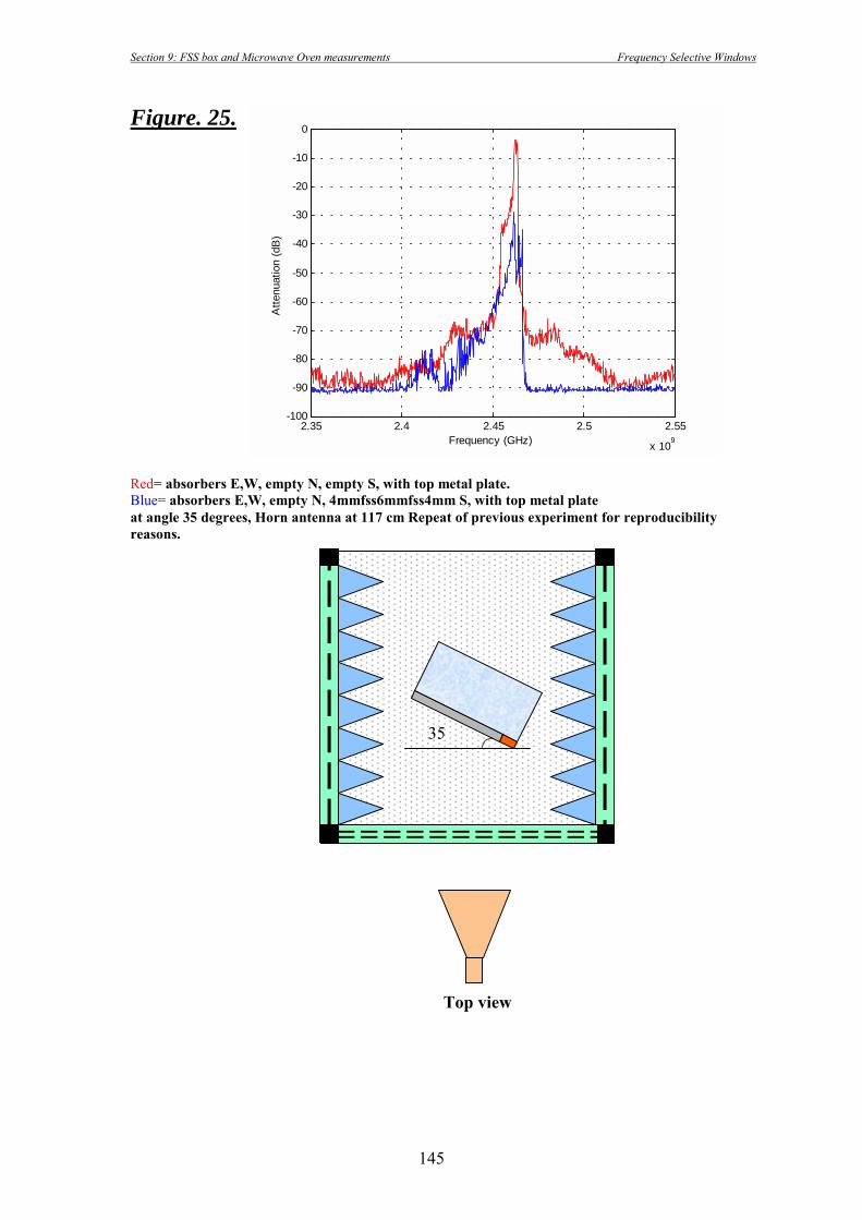
Section 9: FSS box and Microwave Oven measurements Frequency Selective Windows
145
Figure. 25.
Red= absorbers E,W, empty N, empty S, with top metal plate.Blue= absorbers E,W, empty N, 4mmfss6mmfss4mm S, with top metal plateat angle 35 degrees, Horn antenna at 117 cm Repeat of previous experiment for reproducibilityreasons.
Top view
2.35 2.4 2.45 2.5 2.55
x 109
-100
-90
-80
-70
-60
-50
-40
-30
-20
-10
0
Frequency (GHz)
Atte
nuat
ion
(dB
)
35

Section 9: FSS box and Microwave Oven measurements Frequency Selective Windows
146
Figure. 26.
Red= absorbers E,W, empty N, empty S, with top metal plate.Blue= absorbers E,W, empty N, 4mmfss4mm S, with top metal plate.Microwave oven at at angle 35 degrees. Horn antenna at 117 cm.
Top view
35
2.35 2.4 2.45 2.5 2.55
x 109
-100
-90
-80
-70
-60
-50
-40
-30
-20
-10
0
Frequency (GHz)
Atte
nuat
ion
(dB
)

Section 9: FSS box and Microwave Oven measurements Frequency Selective Windows
147
Figure. 27.
Red= absorbers E,W, empty N, empty S, with top metal plate.Blue= absorbers E,W, empty N, 4mmfss4mm S, with top metal plate Microwave oven at angle 35 degrees. Horn antenna at 102 cm.
Top view
2.35 2.4 2.45 2.5 2.55
x 109
-100
-90
-80
-70
-60
-50
-40
-30
-20
-10
0
Frequency (GHz)
Atte
nuat
ion
(dB
)
35

Section 9: FSS box and Microwave Oven measurements Frequency Selective Windows
148
Figure. 28.
Red= absorbers N,E,W, empty S, no top metal plate.Blue=4mmfss4mm N,E,W,S (all around), no top metal plate.Horn antenna at 102 cm.
Top view
2.35 2.4 2.45 2.5 2.55
x 109
-100
-90
-80
-70
-60
-50
-40
-30
-20
-10
0
Frequency (GHz)
Atte
nuat
ion
(dB
)

Section 9: FSS box and Microwave Oven measurements Frequency Selective Windows
149
Figure. 29.
Red=absorbers N,E,W, empty S, no top metal plate.Blue=4mmfss4mm N,E,W, S,(all around), no top metal plate.Horn antenna at 117 cm.
Top view
2.35 2.4 2.45 2.5 2.55
x 109
-100
-90
-80
-70
-60
-50
-40
-30
-20
-10
0
Frequency (GHz)
Atte
nuat
ion
(dB
)

Section 9: FSS box and Microwave Oven measurements Frequency Selective Windows
150
Figure. 30.
Red= absorbers N,E,W, empty S, no top metal plate.Blue=4mmfss4mm N,E,W,S (all around), no top metal plate.Horn antenna at 102 cm.
Top view
2.35 2.4 2.45 2.5 2.55
x 109
-100
-90
-80
-70
-60
-50
-40
-30
-20
-10
0
Frequency (GHz)
Atte
nuat
ion
(dB)

Section 9: FSS box and Microwave Oven measurements Frequency Selective Windows
151
Figure. 31.
Red= absorbers N,E,W, empty S, with top metal plate.Blue=4mmfss4mm N,E,W, S,(all around), with top metal plate.Horn antenna at 117 cm.
Top view
2.35 2.4 2.45 2.5 2.55
x 109
-100
-90
-80
-70
-60
-50
-40
-30
-20
-10
0
Frequency (GHz)
Atte
nuat
ion
(dB
)

Section 9: FSS box and Microwave Oven measurements Frequency Selective Windows
152
Figure. 32.
Red= absorbers N,E,W, empty S, with top metal plate.Blue=4mmfss4mm N,E,W, S,(all around), with top metal plate.Horn antenna at 102 cm.
Top view
2.35 2.4 2.45 2.5 2.55
x 109
-100
-90
-80
-70
-60
-50
-40
-30
-20
-10
0
Frequency (GHz)
Atte
nuat
ion
(dB
)

Section 9: FSS box and Microwave Oven measurements Frequency Selective Windows
153
Figure. 33.
Red= absorbers E,W, empty N, S, with top metal plate.Blue=4mmfss4mm E,W,S, empty N, with top metal plate.Horn antenna at 117 cm.
Top view
2.35 2.4 2.45 2.5 2.55
x 109
-100
-90
-80
-70
-60
-50
-40
-30
-20
-10
0
Frequency (GHz)
Atte
nuat
ion
(dB
)

Section 9: FSS box and Microwave Oven measurements Frequency Selective Windows
154
Figure. 34.
Red= absorbers E,W, empty N, S, with top metal plate.Blue=4mmfss4mm E,W,S, empty N, with top metal plate.Horn antenna at 102 cm.
Top view
2.35 2.4 2.45 2.5 2.55
x 109
-100
-90
-80
-70
-60
-50
-40
-30
-20
-10
0
Frequency (GHz)
Atte
nuat
ion
(dB
)

Section 9: FSS box and Microwave Oven measurements Frequency Selective Windows
155
Figure. 35.
Magenta= absorbers E,W, empty N, S, with top metal plateWith cup of water placed at the centreCyan= absorbers E,W, empty N, S, with top metal plate.Empty turntable, height 102 cm.
Top view
2.35 2.4 2.45 2.5 2.55
x 109
-100
-90
-80
-70
-60
-50
-40
-30
-20
-10
0
Frequency (GHz)
Atte
nuat
ion
(dB
)

Section 9: FSS box and Microwave Oven measurements Frequency Selective Windows
156
Figure. 36.
Magenta= absorbers E,W, empty N, S, with top metal plateWith cup of water placed at the centreCyan= absorbers E,W, empty N, S, with top metal plateEmpty turntable. Horn antenna at 117 cm
Top view
2.35 2.4 2.45 2.5 2.55
x 109
-100
-90
-80
-70
-60
-50
-40
-30
-20
-10
0
Frequency (GHz)
Atte
nuat
ion
(dB
)

Section 9: FSS box and Microwave Oven measurements Frequency Selective Windows
157
Figure. 37.
Repeat twice of the same experiment for reproducibility reasons. Water at the very edge.Horn antenna at height 117 cm. 4mmfss4mm E,W,S, empty N, with top metal plate.
Top view
2.35 2.4 2.45 2.5 2.55
x 109
-100
-90
-80
-70
-60
-50
-40
-30
-20
Frequency (GHz)
Atte
nuat
ion
(dB
)

Section 9: FSS box and Microwave Oven measurements Frequency Selective Windows
158
Figure. 38.
Magenta= absorbers E,W, empty N, S, with top metal plate.Black= absorbers E,W, empty N, S, with top metal plate.With cup of water placed at the edge.Horn antenna at 117 cm.
Top view
2.35 2.4 2.45 2.5 2.55
x 109
-100
-90
-80
-70
-60
-50
-40
-30
-20
-10
0
Frequency (GHz)
Atte
nuat
ion
(dB
)

Section 9: FSS box and Microwave Oven measurements Frequency Selective Windows
159
Figure 39:
Effect of 4mm glass FSS on the transmission of a biconical antenna placed inside the box.Transmitting antenna is the biconical and receiving antenna is the horn with Verticalpolarisation. Red data are the raw data which result from subtraction of calibration withabsorber-NEW empty-S and top metal plate from the ones with 4mmfss all around with topmetal plate.Blue line is the averaged red by every 10 points.
0.5m
Top view
1.5 2 2.5 3 3.5 4 4.5 5 5.5
x 109
-35
-30
-25
-20
-15
-10
-5
0
5
10
15
Frequency (GHz)
Atte
nuat
ion
(dB
)
1.5 2 2.5 3 3.5 4 4.5 5 5.5
x 109
-20
-15
-10
-5
0
5
Frequency (GHz)
Atte
nuat
ion
(dB
)

Section 9: FSS box and Microwave Oven measurements Frequency Selective Windows
160
Figure 40:
Effect of 4mm glass FSS on the transmission of a biconical antenna placed inside the box.Transmitting antenna is the horn with vertical polarisation and receiving antenna is thebiconical.Red data are the raw data which result from subtraction of calibration with absorber-NEW empty-S and top metal plate from the ones with 4mmfss all around with top metal plate.Blue line is the averaged red by every 10 points.
0.5m
Top view
1.5 2 2.5 3 3.5 4 4.5 5
x 109
-35
-30
-25
-20
-15
-10
-5
0
5
10
15
Frequency (GHz)
Atte
nuat
ion
(dB
)
1.5 2 2.5 3 3.5 4 4.5 5
x 109
-20
-15
-10
-5
0
5
Frequency (GHz)
Atte
nuat
ion
(dB
)

Section 9: FSS box and Microwave Oven measurements Frequency Selective Windows
161
Figure 41:
Effect of 4mm glass FSS on the transmission of a biconical antenna placed inside the box.Transmitting antenna is the biconical and receiving antenna is the horn with verticalpolarisation. Measurements were taken around the dip with 1MHz step.
0.5m
Top view
2.4 2.6 2.8 3 3.2 3.4 3.6
x 109
-40
-30
-20
-10
0
10
20
Frequency (GHz)
Atte
nuat
ion
(dB
)
2.4 2.6 2.8 3 3.2 3.4 3.6
x 109
-20
-15
-10
-5
0
5
10
Frequency (GHz)
Atte
nuat
ion
(dB
)

Section 9: FSS box and Microwave Oven measurements Frequency Selective Windows
162
Figure 42:
Effect of 4mm glass FSS on the transmission of a biconical antenna placed inside the box.Transmitting antenna is the biconical at the centre of box and receiving antenna is the horn withvertical polarisation placed at 2m away from the side of box. Red data are the raw data whichresult from subtraction of calibration with absorber-NEW,empty-S and top metal plate from theones with 4mmfss all around with top metal plate.Blue line is the averaged red by every 40 points.
2m
1.5 2 2.5 3 3.5 4 4.5 5
x 109
-40
-30
-20
-10
0
10
20
Frequency (GHz)
Atte
nuat
ion
(dB)
1.5 2 2.5 3 3.5 4 4.5 5
x 109
-15
-10
-5
0
5
10
15
Frequency (GHz)
Atte
nuat
ion
(dB
)

Section 9: FSS box and Microwave Oven measurements Frequency Selective Windows
163
Figure 43:
Effect of 4mm glass FSS on the transmission of a biconical antenna placed inside the box.Transmitting antenna is the biconical at the corner of the box between south and east, andreceiving antenna is the horn with vertical polarisation placed at 2m away from the side of box.Red data are the raw data which result from subtraction of calibration with absorber-NEW,empty-S and top metal plate from the ones with 4mmfss all around with top metal plate.Blue line is the averaged red by every 40 points.
2m
1.5 2 2.5 3 3.5 4 4.5 5
x 109
-40
-30
-20
-10
0
10
20
Frequency (GHz)
Atte
nuat
ion
(dB
)
1.5 2 2.5 3 3.5 4 4.5 5
x 109
-15
-10
-5
0
5
10
Frequency (GHz)
Atte
nuat
ion
(dB)

Section 9: FSS box and Microwave Oven measurements Frequency Selective Windows
164
Figure 44:
Effect of 4mm glass FSS on the transmission of a biconical antenna placed inside the box.Transmitting antenna is the biconical and receiving antenna is the horn with Verticalpolarisation. Absorbers have been placed on opposite sides of FSS windows E, absorber-N withtop metal plate. Red data are the raw data which result from subtraction of calibration withabsorber NEW, empty-S and top metal plate from the ones with 4mmfss all around , absorber-EN and with top metal plate.Blue line is the averaged red by every 10 points.
0.5m
1.5 2 2.5 3 3.5 4 4.5 5
x 109
-40
-35
-30
-25
-20
-15
-10
-5
0
Frequency (GHz)
Atte
nuat
ion
(dB
)
1.5 2 2.5 3 3.5 4 4.5 5
x 109
-30
-25
-20
-15
-10
-5
0
Frequency (GHz) A
ttenu
atio
n (d
B)

Section 9: FSS box and Microwave Oven measurements Frequency Selective Windows
165
Figure 45:-
Effect of 4mm glass FSS on the transmission of a biconical antenna placed inside the box.Transmitting antenna is the biconical in the centre and receiving antenna is the horn withhorizontal polarisation. Measurements with absorbers all around the three sides wheresubtracted from measurements of the box with FSS and horn horizontally polarised.
Top view
1.5 2 2.5 3 3.5 4 4.5 5
x 109
-45
-40
-35
-30
-25
-20
-15
-10
-5
Frequency (GHz)
Atte
nuat
ion
(dB)
1.5 2 2.5 3 3.5 4 4.5 5
x 109
-30
-28
-26
-24
-22
-20
-18
-16
-14
-12
-10
Frequency (GHz)
Atte
nuat
ion
(dB
)

Section 9: FSS box and Microwave Oven measurements Frequency Selective Windows
166
Figure 46:
Red= raw data represents subtraction of data with Tx=horn Vp outside 50 cm away and withRx=biconical inside and absorber-NEW from same configuration but with absorbers gone andreplaced with 4mm fss N,E,W,S metal top.Blue=red averaged by every 10 points
0.5m
Top view
2.4 2.6 2.8 3 3.2 3.4 3.6
x 109
-40
-30
-20
-10
0
10
20
Frequency (GHz)
Att
enua
tion
(dB
)
2.4 2.6 2.8 3 3.2 3.4 3.6
x 109
-25
-20
-15
-10
-5
0
5
10
Frequency (GHz)
Att
enua
tion
(dB
)

Section 9: FSS box and Microwave Oven measurements Frequency Selective Windows
167