FreeForm/Express - Connect Tech Inc.
35
Connect Tech Inc. | FreeForm/Express S6 - PCIe Spartan-6 FMC Carrier | User Manual CTIM-00062 Revision 0.03 1 FreeForm/Express S6 PCIe Spartan-6 FMC Carrier Connect Tech Inc. Tel: 519-836-1291 42 Arrow Road Toll: 800-426-8979 (North America only) Guelph, Ontario Fax: 519-836-4878 N1K 1S6 Email: [email protected] www.connecttech.com [email protected] CTIM-00062 Revision 0.03 2020-02-01
Transcript of FreeForm/Express - Connect Tech Inc.

Connect Tech Inc. | FreeForm/Express S6 - PCIe Spartan-6 FMC Carrier | User Manual
CTIM-00062 Revision 0.03 1
FreeForm/Express S6 PCIe Spartan-6 FMC Carrier
Connect Tech Inc. Tel: 519-836-1291
42 Arrow Road Toll: 800-426-8979 (North America only) Guelph, Ontario Fax: 519-836-4878 N1K 1S6 Email: [email protected] www.connecttech.com [email protected] CTIM-00062 Revision 0.03 2020-02-01

FreeForm/Express
Users Guide
www.connecttech.com
Document: CTIM-00062
Revision: 0.03
Page 2 of 35
Connect Tech Inc. 800-426-8979 | 519-836-1291
Date: 2020-02-01
Table of Contents Customer Support Overview .......................................................................................................................... 3
Contact Information........................................................................................................................................ 3
Limited Lifetime Warranty ............................................................................................................................. 5
Copyright Notice ............................................................................................................................................ 5
Trademark Acknowledgment ......................................................................................................................... 5
Revision History ............................................................................................................................................. 5
Introduction .................................................................................................................................................... 6
Features ................................................................................................................................................... 6
What is an FPGA Mezzanine Card (FMC)? ............................................................................................ 6
System Block Diagram ............................................................................................................................ 7
Hardware Description ..................................................................................................................................... 8
FPGA....................................................................................................................................................... 8
PCI Express Bus ...................................................................................................................................... 8
Memory & Flash ..................................................................................................................................... 8
Low Pin Count FMC Interface ................................................................................................................ 9
Configuration .........................................................................................................................................13
Ethernet ..................................................................................................................................................15
Serial ......................................................................................................................................................16
Power......................................................................................................................................................16
Hardware Installation ....................................................................................................................................17
Standard computer ..................................................................................................................................17
Software Installation ......................................................................................................................................17
Cables & Interconnect ...................................................................................................................................18
Mating Cables ........................................................................................................................................18
Mating Connectors .................................................................................................................................18
Reference Design ..........................................................................................................................................19
FPGA Design .........................................................................................................................................20
Top Level ........................................................................................................................................ 20 Memory Interface ............................................................................................................................ 21 PCI Express Interface ...................................................................................................................... 21 Ethernet MAC Interface .................................................................................................................. 22 FMC I/O .......................................................................................................................................... 23 SPI Flash Interface .......................................................................................................................... 23 Serial Interface ................................................................................................................................ 24 Address Map ................................................................................................................................... 25
Example software Applications ..............................................................................................................28
Windows Notes ............................................................................................................................... 28 Linux Notes ..................................................................................................................................... 28
FPGA Pinout .................................................................................................................................................29
Specifications ................................................................................................................................................35

FreeForm/Express
Users Guide
www.connecttech.com
Document: CTIM-00062
Revision: 0.03
Page 3 of 35
Connect Tech Inc. 800-426-8979 | 519-836-1291
Date: 2020-02-01
Preface
Disclaimer
The information contained within this user’s guide, including but not limited to any product
specification, is subject to change without notice.
Connect Tech assumes no liability for any damages incurred directly or indirectly from any
technical or typographical errors or omissions contained herein or for discrepancies between the
product and the user’s guide.
Customer Support Overview
If you experience difficulties after reading the manual and/or using the product, contact the
Connect Tech reseller from which you purchased the product. In most cases the reseller can help
you with product installation and difficulties.
In the event that the reseller is unable to resolve your problem, our highly qualified support staff
can assist you. Our support section is available 24 hours a day, 7 days a week on our website at:
www.connecttech.com/sub/support/support.asp. See the contact information section below for
more information on how to contact us directly. Our technical support is always free.
Contact Information
We offer three ways for you to contact us:
Mail/Courier
You may contact us by letter at:
Connect Tech Inc.
Technical Support
42 Arrow Road
Guelph, Ontario
Canada N1K 1S6
Email/Internet
You may contact us through the Internet. Our email and URL addresses on the Internet are:
www.connecttech.com
Note:
Please go to the Download Zone or the Knowledge Database in the Support Center on the Connect
Tech website for product manuals, installation guides, device driver software and technical tips.
Submit your technical support questions to our customer support engineers via the Support Center on the Connect Tech website.
Telephone/Facsimile
Technical Support representatives are ready to answer your call Monday through Friday, from
8:30 a.m. to 5:00 p.m. Eastern Standard Time. Our numbers for calls are:

FreeForm/Express
Users Guide
www.connecttech.com
Document: CTIM-00062
Revision: 0.03
Page 4 of 35
Connect Tech Inc. 800-426-8979 | 519-836-1291
Date: 2020-02-01
Toll Free: 800-426-8979 (North America only)
Telephone: 519-836-1291 (Live assistance available 8:30 a.m. to 5:00 p.m. EST,
Monday to Friday)
Facsimile: 519-836-4878 (on-line 24 hours)

FreeForm/Express
Users Guide
www.connecttech.com
Document: CTIM-00062
Revision: 0.03
Page 5 of 35
Connect Tech Inc. 800-426-8979 | 519-836-1291
Date: 2020-02-01
Limited Lifetime Warranty
Connect Tech Inc. provides a Lifetime Warranty for all Connect Tech Inc. products. Should this
product, in Connect Tech Inc.'s opinion, fail to be in good working order during the warranty
period, Connect Tech Inc. will, at its option, repair or replace this product at no charge, provided
that the product has not been subjected to abuse, misuse, accident, disaster or non-Connect Tech
Inc. authorized modification or repair.
You may obtain warranty service by delivering this product to an authorized Connect Tech Inc.
business partner or to Connect Tech Inc. along with proof of purchase. Product returned to
Connect Tech Inc. must be pre-authorized by Connect Tech Inc. with an RMA (Return Material
Authorization) number marked on the outside of the package and sent prepaid, insured and
packaged for safe shipment. Connect Tech Inc. will return this product by prepaid ground
shipment service.
The Connect Tech Inc. Lifetime Warranty is defined as the serviceable life of the product. This is
defined as the period during which all components are available. Should the product prove to be
irreparable, Connect Tech Inc. reserves the right to substitute an equivalent product if available or
to retract Lifetime Warranty if no replacement is available.
The above warranty is the only warranty authorized by Connect Tech Inc. Under no
circumstances will Connect Tech Inc. be liable in any way for any damages, including any lost
profits, lost savings or other incidental or consequential damages arising out of the use of, or
inability to use, such product.
Copyright Notice
The information contained in this document is subject to change without notice. Connect Tech
Inc. shall not be liable for errors contained herein or for incidental consequential damages in
connection with the furnishing, performance, or use of this material. This document contains
proprietary information that is protected by copyright. All rights are reserved. No part of this
document may be photocopied, reproduced, or translated to another language without the prior
written consent of Connect Tech Inc.
Copyright © 1997 - 2020 by Connect Tech Inc.
Trademark Acknowledgment
Connect Tech Inc. acknowledges all trademarks, registered trademarks and/or copyrights referred
to in this document as the property of their respective owners.
Not listing all possible trademarks or copyright acknowledgments does not constitute a lack of
acknowledgment to the rightful owners of the trademarks and copyrights mentioned in this
document.
Revision History
Revision 0.00 – 2011-01-26
Revision 0.01 – 2011-06-27
Revision 0.02 – 2012-03-12
Revision 0.03 – 2020-02-01

FreeForm/Express
Users Guide
www.connecttech.com
Document: CTIM-00062
Revision: 0.03
Page 6 of 35
Connect Tech Inc. 800-426-8979 | 519-836-1291
Date: 2020-02-01
Introduction
Connect Tech’s FreeForm/Express S6 is a reconfigurable computing platform that is based on the
Xilinx Spartan-6 FPGA; featuring integrated PCI Express® blocks, advanced memory support,
and 3.125 Gbps low-power transceivers. The FreeForm/Express S6 includes an industry-standard
FPGA Mezzanine Card (FMC) connector, which provides a flexible I/O interface for future
scaling and customization. The PCIe bus bandwidth ensures high speed communication between
the host system and the application’s interfaces.
A wide range of available FMC modules adds interfaces such as ADC and digital video, which
makes the FreeForm/Express S6 a highly versatile platform for system development. It is ideally
suited for applications requiring both prototyping and field deployment including real-time data
acquisition, high performance video processing, and software defined radio. The
FreeForm/Express S6 is optimized for embedded processor designs, supporting development with
Xilinx’s MicroBlaze.
Features
• Spartan-6 LX45T FPGA
• PCIe x1 form factor
• 128MB DDR3 Memory
• Low Pin Count FMC connector
o 36 LVDS pairs
o 1 Rocket I/O channel
o I2C interface
• 2x 10/100/1000 Ethernet ports
• 1x RS-232 port
• 4 MB Flash for FPGA configuration
• 2 MB Flash for embedded code storage
• 200 MHz oscillator
• JTAG debugging
• Industrial temperature (-40 to 85C)
• Lifetime warranty and free technical support.
What is an FPGA Mezzanine Card (FMC)?
An FPGA Mezzanine Card (FMC) is a standard created by VITA (VMEbus International Trade
Association). The FMC standard (VITA 57.1) defines a module size and connector interface with
generic reconfigurable I/O, making it perfect for FPGA daughter board applications. The standard
defines two pin-outs, low pin count (LPC) and high pin count (HPC); with each type using the
same connector form factor.
For more information visit http://www.vita.com/fmc.html.

FreeForm/Express
Users Guide
www.connecttech.com
Document: CTIM-00062
Revision: 0.03
Page 7 of 35
Connect Tech Inc. 800-426-8979 | 519-836-1291
Date: 2020-02-01
System Block Diagram
The following block diagram depicts component and connector interconnect, along with the appropriate
bus definitions.

FreeForm/Express
Users Guide
www.connecttech.com
Document: CTIM-00062
Revision: 0.03
Page 8 of 35
Connect Tech Inc. 800-426-8979 | 519-836-1291
Date: 2020-02-01
Hardware Description
FPGA
Description The FreeForm/Express S6 features the Xilinx Spartan-6 LX45T FPGA in a 484 pin BGA package
(Xilinx XC6SLX45T-2FGG484I). The Spartan-6 simplifies FPGA design by providing a
integrated memory controller and PCI express end point, along with high performance general I/O,
clocking, and internal memory resources comparable to be previous generation Virtex-class
FPGAs.
For more details on the Spartan-6 capabilities, visit:
http://www.xilinx.com/products/spartan6/index.htm.
Function LEDs
Locations Pin Signal
D14 Memory controller Error [*]
D15 Memory controller calibration done [*]
D8 User LED 0 [*]
D5 System reset active [*]
D6 Link training reset active [*]
D7 PCIe Linked [*]
D4 FPGA configuration done
[*] LED function is depends on loaded FPGA configuration, these represent status exhibited by the FreeForm/Express default reference design
PCI Express Bus
Description The FreeForm/Express S6 has a single x1 PCIe express lane, connected directly to the Spartan-6
FPGA. The PCIe interface is facilitated by the Spartan-6’s integrated PCI express endpoint.
Memory & Flash
Description A single 1024 Mbit x16 DDR3 component (Micron MT41J64M16JT-15E) is connected to the
Spartan-6 FPGA, providing 128 MB of high speed memory. The Spartan-6’s integrated memory
controller provides a generic high speed interface to FPGA logic.
In addition, a 16 Mbit SPI flash component (Numonyx M25P16) is connected to the FPGA’s user
I/O for storage of embedded processor code.

FreeForm/Express
Users Guide
www.connecttech.com
Document: CTIM-00062
Revision: 0.03
Page 9 of 35
Connect Tech Inc. 800-426-8979 | 519-836-1291
Date: 2020-02-01
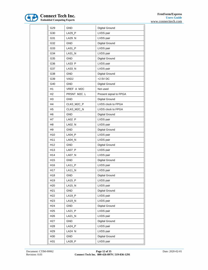
Low Pin Count FMC Interface
Description The FreeForm/Express S6 provides a single Low Pin Count FPGA Mezzanine Card (FMC) Interface.
The LPC connector provides the following features
• 36 LVDS pairs, 2 designated as global clocks (or 68 2.5V LVCMOS pairs)
• I2C interface
• 1 SERDES TX / RX channel (Rocket I/O , GTP), with clock
• Power : +12VDC, +3.3V DC, +2.5V DC
The FreeForm/Express S6 LPC implementation differs from the VITA 57.1 specification as follows:
• VADJ is fixed to +2.5 V DC
• Only LVDS or 2.5V LVCMOS I/O is supported.
Connector
Function LPC FMC
Location P7
Type Samtec ASP-134603-01
Pinout
Pin Signal Description
C1 GND Digital Ground
C2 DP0_C2M_P Serdes pair from FPGA
C3 DP0_C2M_N Serdes pair from FPGA
C4 GND Digital Ground
C5 GND Digital Ground
C6 DP0_M2C_P Serdes pair to FPGA
C7 DP0_M2C_N Serdes pair to FPGA
C8 GND Digital Ground
C9 GND Digital Ground
C10 LA06_P LVDS pair
C11 LA06_N LVDS pair
C12 GND Digital Ground
C13 GND Digital Ground
C14 LA10_P LVDS pair
C15 LA10_N LVDS pair
C16 GND Digital Ground
C17 GND Digital Ground
C18 LA14_P LVDS pair
C19 LA14_N LVDS pair
C20 GND Digital Ground
C21 GND Digital Ground
C22 LA18_P_CC LVDS clock capable pair

FreeForm/Express
Users Guide
www.connecttech.com
Document: CTIM-00062
Revision: 0.03
Page 10 of 35
Connect Tech Inc. 800-426-8979 | 519-836-1291
Date: 2020-02-01
C23 LA18_N_CC LVDS clock capable pair
C24 GND Digital Ground
C25 GND Digital Ground
C26 LA27_P LVDS pair
C27 LA27_N LVDS pair
C28 GND Digital Ground
C29 GND Digital Ground
C30 SCL I2C clock
C31 SDA I2C data
C32 GND Digital Ground
C33 GND Digital Ground
C34 GA0 I2C address
C35 12P0V +12V DC
C36 GND Digital Ground
C37 12P0V +12V DC
C38 GND Digital Ground
C39 3P3V +3.3V DC
C40 GND Digital Ground
D1 PG_C2M Power good
D2 GND Digital Ground
D3 GND Digital Ground
D4 GBTCLK0_M2C_P Serdes clock to FPGA
D5 GBTCLK0_M2C_N Serdes clock to FPGA
D6 GND Digital Ground
D7 GND Digital Ground
D8 LA01_P_CC LVDS clock capable pair
D9 LA01_N_CC LVDS clock capable pair
D10 GND Digital Ground
D11 LA05_P LVDS pair
D12 LA05_N LVDS pair
D13 GND Digital Ground
D14 LA09_P LVDS pair
D15 LA09_N LVDS pair
D16 GND Digital Ground
D17 LA13_P LVDS pair
D18 LA13_N LVDS pair
D19 GND Digital Ground
D20 LA17_P_CC LVDS clock capable pair
D21 LA17_N_CC LVDS clock capable pair
D22 GND Digital Ground
D23 LA23_P LVDS pair
D24 LA23_N LVDS pair
D25 GND Digital Ground

FreeForm/Express
Users Guide
www.connecttech.com
Document: CTIM-00062
Revision: 0.03
Page 11 of 35
Connect Tech Inc. 800-426-8979 | 519-836-1291
Date: 2020-02-01
D26 LA26_P LVDS pair
D27 LA26_N LVDS pair
D28 GND Digital Ground
D29 TCK JTAG
D30 TDI JTAG
D31 TDO JTAG
D32 3P3VAUX +3.3V DC
D33 TMS JTAG
D34 TRST_L JTAG
D35 GA1 I2C address
D36 3P3V +3.3V DC
D37 GND Digital Ground
D38 3P3V +3.3V DC
D39 GND Digital Ground
D40 3P3V +3.3V DC
G1 GND Digital Ground
G2 CLK1_M2C_P LVDS clock to FPGA
G3 CLK1_M2C_N LVDS clock to FPGA
G4 GND Digital Ground
G5 GND Digital Ground
G6 LA00_P_CC LVDS clock capable pair
G7 LA00_N_CC LVDS clock capable pair
G8 GND Digital Ground
G9 LA03_P LVDS pair
G10 LA03_N LVDS pair
G11 GND Digital Ground
G12 LA08_P LVDS pair
G13 LA08_N LVDS pair
G14 GND Digital Ground
G15 LA12_P LVDS pair
G16 LA12_N LVDS pair
G17 GND Digital Ground
G18 LA16_P LVDS pair
G19 LA16_N LVDS pair
G20 GND Digital Ground
G21 LA20_P LVDS pair
G22 LA20_N LVDS pair
G23 GND Digital Ground
G24 LA22_P LVDS pair
G25 LA22_N LVDS pair
G26 GND Digital Ground
G27 LA25_P LVDS pair
G28 LA25_N LVDS pair
FreeForm/Express
Users Guide
www.connecttech.com
Document: CTIM-00062
Revision: 0.03
Page 12 of 35
Connect Tech Inc. 800-426-8979 | 519-836-1291
Date: 2020-02-01
G29 GND Digital Ground
G30 LA29_P LVDS pair
G31 LA29_N LVDS pair
G32 GND Digital Ground
G33 LA31_P LVDS pair
G34 LA31_N LVDS pair
G35 GND Digital Ground
G36 LA33_P LVDS pair
G37 LA33_N LVDS pair
G38 GND Digital Ground
G39 VADJ +2.5V DC
G40 GND Digital Ground
H1 VREF_A_M2C Not used
H2 PRSNT_M2C_L Present signal to FPGA
H3 GND Digital Ground
H4 CLK0_M2C_P LVDS clock to FPGA
H5 CLK0_M2C_N LVDS clock to FPGA
H6 GND Digital Ground
H7 LA02_P LVDS pair
H8 LA02_N LVDS pair
H9 GND Digital Ground
H10 LA04_P LVDS pair
H11 LA04_N LVDS pair
H12 GND Digital Ground
H13 LA07_P LVDS pair
H14 LA07_N LVDS pair
H15 GND Digital Ground
H16 LA11_P LVDS pair
H17 LA11_N LVDS pair
H18 GND Digital Ground
H19 LA15_P LVDS pair
H20 LA15_N LVDS pair
H21 GND Digital Ground
H22 LA19_P LVDS pair
H23 LA19_N LVDS pair
H24 GND Digital Ground
H25 LA21_P LVDS pair
H26 LA21_N LVDS pair
H27 GND Digital Ground
H28 LA24_P LVDS pair
H29 LA24_N LVDS pair
H30 GND Digital Ground
H31 LA28_P LVDS pair

FreeForm/Express
Users Guide
www.connecttech.com
Document: CTIM-00062
Revision: 0.03
Page 13 of 35
Connect Tech Inc. 800-426-8979 | 519-836-1291
Date: 2020-02-01
H32 LA28_N LVDS pair
H33 GND Digital Ground
H34 LA30_P LVDS pair
H35 LA30_N LVDS pair
H36 GND Digital Ground
H37 LA32_P LVDS pair
H38 LA32_N LVDS pair
H39 GND Digital Ground
H40 VADJ +2.5V DC
Configuration
The FreeForm/Express S6 is designed so that the Spartan-6 configuration image is automatically loaded
from the on-board SPI flash at power- up. When a valid configuration is loaded, led D4 is illuminated.
JTAG configuration can be used at any time to program the FPGA.
The FreeForm/Express S6 is fitted with a x4 32 Mbit SPI flash (W25Q32BVSFIG or S25FL064), which
can be programmed indirectly via JTAG using Xilinx’s IMPACT.
Function JTAG programming
Location P5
Type 1x7 0.100” header
Samtec TSW-107-08-F-S-RA
Pinout
Pin Signal Description
1 TRST# Reset, not used by Xilinx products
2 TMS Select
3 TDI Data In
4 TDO Data Out
5 TCK Clock
6 GND Digital Ground
7 VCC Chain power, 3.3V
Function Manual Reset
Pulls the Spartan-6 PROG_B pin to ground, resetting and
reconfiguring the FPGA
Location J1
Type 1x2 0.100” jumper block
Pinout Position Description
1-2 +5V
off floating
Default Floating

FreeForm/Express
Users Guide
www.connecttech.com
Document: CTIM-00062
Revision: 0.03
Page 14 of 35
Connect Tech Inc. 800-426-8979 | 519-836-1291
Date: 2020-02-01
Function Hot Swap
When the is being configured, FPGA I/Os will be pulled
high with weak internal pull-ups
Location J2
Type 1x2 0.100” jumper block
Pinout Position Description
1-2 I/Os have pullups
off I/Os are floating
Default Floating
Function FMC JTAG Bypass
Selects either whether or not to include the FMC module
in the JTA chain
Location J3
Type 2x2 0.100” jumper block
Pinout Position Description
1-3 TDI to FMC
2-4 TDO from FMC
3-4 Bypass
off Not applicable
Default Bypass

FreeForm/Express
Users Guide
www.connecttech.com
Document: CTIM-00062
Revision: 0.03
Page 15 of 35
Connect Tech Inc. 800-426-8979 | 519-836-1291
Date: 2020-02-01
Ethernet
Description Two 10/100/1000 Ethernet ports are connected to the FPGA, via two separate RGMII capable Ethernet
physical layer devices (PHYs). The FPGA logic resources are used to implement the Ethernet media
access controller (MAC).
Connector & LEDs
Function Ethernet
Location P6A, P6B
Type 2x5 2mm header
MLE TSHSM-205-D-06-G-V-L (or equivalent)
Pinout
Pin Signal Description Pin Signal Description
1 MX1- Data 2 MX1+ Data
3 MX2- Data 4 MX2+ Data
5 FGND Frame Ground
6 FGND Frame Ground
7 MX3- Data 8 MX3+ Data
9 MX4- Data 10 MX4+ Data
Function Ethernet Status LEDs
Locations Pin Signal
D16A ETH0 Activity
D17A ETH0 Link
D16B ETH1 Activity
D17B ETH1 Link

FreeForm/Express
Users Guide
www.connecttech.com
Document: CTIM-00062
Revision: 0.03
Page 16 of 35
Connect Tech Inc. 800-426-8979 | 519-836-1291
Date: 2020-02-01
Serial
Description A standard RS232 serial ports is provided on P4, with UART implementation provided by FPGA logic.
Connectors
Function RS232
Locations P4
Type 2x5 0.100” header
Samtec TSW-105-07-L-D
Pinout Pin Signal Pin Signal
1 N/C 2 N/C
3 RXD1 4 RTS1
5 TXD1 6 CTS1
7 N/C 8 N/C
9 GND 10 N/C
Power
Description The FreeForm/Express S6 is designed to be powered from the PCIe bus. The board requires +3.3V DC for
all circuitry. +12VDC is required for the FMC power good signal and as the FMC module’s power source.
The FreeForm/Express S6 generates all other required power rails on-board.
In addition, a programming / desktop debugging standalone power connector P1 is provided.
WARNING: Do not plug the FreeForm/Express S6 into a PCIe slot with an external power source
connected to P1. This could lead to board damage and void the product warranty.
Connectors & Jumpers
Function Standalone power
Location P1
Type 2x3 0.100” power header, shrouded
Samtec IPL1-103-01-L-D-RA-K
Pinout Pin Signal Description
1 GND Digital Ground
2 GND Digital Ground
3 GND Digital Ground
4 +3.3V +3.3V DC, used by circuitry and power regulators
5 +3.3V +3.3V DC, used by circuitry and power regulators
6 +12V +12V DC used by FMC module, and power good circuit
FreeForm/Express
Users Guide
www.connecttech.com
Document: CTIM-00062
Revision: 0.03
Page 17 of 35
Connect Tech Inc. 800-426-8979 | 519-836-1291
Date: 2020-02-01
Hardware Installation
Standard computer
1. Ensure all computer power supplies are off and disconnected (remove AC line cord)
2. Install the FMC module, if required.
3. Verify all jumper settings from the relevant sections
4. Install the necessary cables for the application.
WARNING: Do not plug the FreeForm/Express S6 into a PCIe slot with an external power source
connected to P1. This could lead to board damage and void the product warranty.
5. Install the FreeForm/Express S6 module into x1 PCIe slot.
6. Connect the appropriate interface cables to the FMC bracket I/O.
7. Connect the computer’s AC line cord to the computer’s power supply.
8. Turn on the computer system.
Software Installation
The FreeForm/Express is fully supported by Connect Tech’s Universal FPGA Driver (UFD). The UFD is
available for download from the Connect Tech’s download zone:
http://www.connecttech.com/asp/Support/DownloadZone.asp
The UFD is available for multiple operating systems; refer to the website for availability and check back
for the latest releases.

FreeForm/Express
Users Guide
www.connecttech.com
Document: CTIM-00062
Revision: 0.03
Page 18 of 35
Connect Tech Inc. 800-426-8979 | 519-836-1291
Date: 2020-02-01
Cables & Interconnect
Mating Cables
Description Location PCB Connector Cable Part Number [Drawing Number]
PCB End Interface End
Power P1 Samtec IPL1-103-01-L-D-RA-K
Samtec MMSD-03-20-L-03.25-S-K
2x3 IPD Un-terminated
Serial P4 Samtec TSW-105-07-L-D
CAG104 [ CTIC-00048 ]
2x5 0.100” IDC DB-9
GBE P6A, P6B MLE TSHSM-205-D-06-G-V-L
CBG065 [CTIC-00181 ]
2x5 2mm socket RJ45 socket
Cable drawings are available upon request
Mating Connectors
Description Location PCB Connector Mating Connector Note
FMC P7 Samtec ASP-134603-01 Samtec ASP-134604-01
10 mm stack
Samtec ASP-134606-01
8.5 mm stack

FreeForm/Express
Users Guide
www.connecttech.com
Document: CTIM-00062
Revision: 0.03
Page 19 of 35
Connect Tech Inc. 800-426-8979 | 519-836-1291
Date: 2020-02-01
Reference Design
The FreeForm/Express S6 is shipped pre-programmed with a reference design, which facilitates the
operation and connectivity to various features to / from the FPGA.
The reference design consists of a FPGA configuration and supporting software example applications. The
sources for both are available through Connect Tech’s development center: http://devel.connecttech.com
In most cases, the FPGA’s peripheral interfaces are mapped directly in the PCI express address space and
controlled directly via software. While this not a likely use case for most application; it does provide an
example on how to design FPGA modules to interact with the memory, flash, and Ethernet peripherals.

FreeForm/Express
Users Guide
www.connecttech.com
Document: CTIM-00062
Revision: 0.03
Page 20 of 35
Connect Tech Inc. 800-426-8979 | 519-836-1291
Date: 2020-02-01
FPGA Design
The FreeForm/Express reference design is based on a combination of modified Xilinx coregent outputs and
original design files. The follow sections detail the hierarchy and description of each peripheral sub-
module.
Top Level
The top level FPGA module (ref_design.vhd) consists of the PCIe end point wrapper (u_pcie), the
input/output memory & register map (u_pio) and the peripheral top level modules. All modules are
connected to a modified version of the PIO (programmed input / output) interface provided with Xilinx
PCIe designs.
The PIO interface is manages the access to attached registers, block memories, and FIFOs; decoupling
other interfaces from the PCIe state machine.
Hierarchy
Block Diagram
Module Description Module
(instance name) Description
u_mig_top DDR3 memory controller, based on MIG 3.6
u_pcie Spartan-6 PCIe
u_pio PIO Application level Register / Memory Interface
u_fmc FMC I/O controller, based on GTP Wizard 1.7
u_mac0, u_mac1 Ethernet controller, based Tri Mode Ethernet MAC 4.4
u_spi SPI Flash controller
u_serial Simple UART

FreeForm/Express
Users Guide
www.connecttech.com
Document: CTIM-00062
Revision: 0.03
Page 21 of 35
Connect Tech Inc. 800-426-8979 | 519-836-1291
Date: 2020-02-01
Memory Interface
This module is modified version of the DDR3 MIG 1.7; connected to the PIO interface
Hierarchy
Module Description Module
(instance name) Description
u_mig_top Memory controller top level; contains necessary clocking adjustments from standard Xilinx wizard generated files
u_mig_pio State machine interface to the memory controller
u_mig_user MIG user top level
memc3_wrapper_inst DDR3 top level wrapper
memc3_infrastructure DDR3 clocking files
others As included with MIG
mig.ucf Associated constraints
PCI Express Interface
This module is a modified version of the Xilinx Spartan-6 Integrated Block for PCI Express v1.4.
Hierarchy
Module Description Module
(instance name) Description
u_pcie Module top level; connects application state machine to endpoint
app PCIe application top level
PIO_i Wrapper for PIO_EP_i
PIO_EP_i Wrapper for EP_RX, EP_TX
EP_RX endpoint receive state machine, modified for larger packets
EP_TX endpoint transmit state machine, modified for larger packets
pcie_i PCIe endpoint top level, instantiates PCIE_A1 hard IP. Modified to expose the 2nd GTP channel.
GT_i Rocket I/O (GTP) instance wrapper

FreeForm/Express
Users Guide
www.connecttech.com
Document: CTIM-00062
Revision: 0.03
Page 22 of 35
Connect Tech Inc. 800-426-8979 | 519-836-1291
Date: 2020-02-01
pcie.ucf Associated constraints
Ethernet MAC Interface
This module is modified and wrapped version of the Tri Mode Ethernet MAC 4.4; connected to the PIO
interface.
Hierarchy
Module Description Module
(instance name) Description
u_mac0, u_mac1 Module top level; connects application state machine to MAC
u_ll_pio Map local link interface to application interface
u_lltx Local transmit statemachine and FIFO
u_llrx Local link receive statemachine and FIFO
u_ll_rgmii Wrapper and clock mapping
trimac_locallink Wrapper, connects client FIFO to TEMAC. Generates resets
trimac_block Wrapper, connects rgmii interface to core
trimac_core Actual core; encrypted. Requires license from Xilinx
rgmii_interface Converts RGMII to GMII
reset_sync Reset synchronizer between clock domains
client_side_FIFO FIFO between local link interface and MAC
others As generated by coregen

FreeForm/Express
Users Guide
www.connecttech.com
Document: CTIM-00062
Revision: 0.03
Page 23 of 35
Connect Tech Inc. 800-426-8979 | 519-836-1291
Date: 2020-02-01
FMC I/O
This module is intended to mimic an actual FMC interface; exercising all the FMC LVDS and SERDES
I/O. It works in conjunction with an external loopback board, which essentially wraps the even numbered
pairs to the odd numbered pairs as well as the SERDES TX to RX.
Hierarchy
Module Description Module
(instance name) Description
u_fmc Top level module
u_fmc_lvds_tx LVDS Transmitter state machine and FIFO, sends data packet over even number pairs
u_fmc_lvds_rx LVDS receiver state machine and FIFO, receives data packets on odd number pairs
u_fmc_gtp_tx GTP transmitter state machine and FIFO. Shares the GTP tile with the PCIe link
u_fmc_gtp_rx GTP receiver state machine and FIFO
fmc.ucf Associated constraints
SPI Flash Interface
This module communicates to x1 SPI flash; for programming and read back purposes. It is based on a
Picoblaze micro-controller, implemented most of the flash commands. It is connected to the PIO interface.
Hierarchy
Module Description Module
(instance name) Description
u_spio Wrappers and instantiation of block memory
processor Picoblaze processor, Spartan-6 version
program_rom Picoblaze program ROM, generated from assembly code
u_txfifo Transmit FIFO between Picoblaze and SPI serializer
u_rxfifo Receive FIFO between Picoblaze and SPI de-serializer
u_spi_ctrl_a, u_spi_ctrl_b
SPI serializer / deserializer; based on Xilinx code
u_dpram Dual port SPI page RAM ; used by application interface and Picoblaze

FreeForm/Express
Users Guide
www.connecttech.com
Document: CTIM-00062
Revision: 0.03
Page 24 of 35
Connect Tech Inc. 800-426-8979 | 519-836-1291
Date: 2020-02-01
Serial Interface
This module implements a very basic UART / serial port; mapping simple controls into the PCI express
address space, via the PIO interface. It is not intended to be compatible with any existing 8250 drivers.
Hierarchy
Module Description
Module (instance name)
Description
u_serial Register mapping, UART instantiation, and baud generation
u_uart Stripped 16550 UART
u_tf Transmit FIFO
u_rf Receive FIFO
u_txsm Transmit State machine
u_rxsm Receive State machine

FreeForm/Express
Users Guide
www.connecttech.com
Document: CTIM-00062
Revision: 0.03
Page 25 of 35
Connect Tech Inc. 800-426-8979 | 519-836-1291
Date: 2020-02-01
Address Map
The following address map shows describes the function and location of each register and memory (Block
RAM or FIFO) used throughout the FPGA design
Offset start
Offset end
Name Type 31 …………. 24 23 …………. 16 15 …………. 08 07 …………. 00
Registers
0000 0003 REVISION R Revision Number Build Number; auto generated with every synthesis run
0007 0004 LED_CONTROL RW GIGE_STATS_SEL 0: User LED 0 1: User LED 1 2: User LED 2
0008 000B FMC_LA_OUTL RW Output Pin state for FMC LA 33-0 , only even number pairs are outputs
000C 000F FMC_LA_OUTH RW
0010 0013 FMC_LA_INL R Input pin state for FMC LA 33-0 , only odd number pairs are outputs
0014 0017 FMC_LA_INH R
0018 001B FMC_MODE_CONTROL RW TX Packet size in bytes Control flags 0: bypass transmitter and receiver state machine for direct pin control 1: internal loopback 2: LVDS TX send 3: LVDS RX ready 4: GTP TX start 5: GTP RX Enable
001C 001F FMC_STATUS R RX packet size in bytes Status flags 0: LVDS TX done 1: LVDS RX done 2: GTP TX done 3: GTP RX done 4: GTP PLL good 5: GTP reset complete
0020 0023 MCB_CONTROL RW Memory controller control flags 0: command FIFO write strobe
0024 0027 MCB_STATUS R Read FIFO Count Write FIFO Count FIFO and misc status flags 0: command FIFO empty 1: command FIFO full 2: Write FIFO full 3: Write FIFO empty 4: Write FIFO underrun 5: Write error 6: Read FIFO full 7: Read FIFO empty 8: Read FIFO overflow 9: Read error 10: Calibration done
0028 002B MCB_CMD RW Memory controller command 2-0: instruction 8-3: burst length
002C 002F MCB_ADDR RW 29-0: Linear memory address
0030 0033 GIGE0_CTRL RW GIGE0_TX_SZ Transmit packet size in bytes
GIGE0_RX_CTRL Receive Control 1: Soft Reset 0: Packet Retrieved
GIGE0_TX_CTRL Transmit Control 1: Soft reset 0: Send Packet
0034 0037 GIGE0_STATUS R GIGE0_RX_SZ Received packet size in bytes
GIGE0_RX_STAT Receive Status
GIGE0_TX_STAT Transmit Status

FreeForm/Express
Users Guide
www.connecttech.com
Document: CTIM-00062
Revision: 0.03
Page 26 of 35
Connect Tech Inc. 800-426-8979 | 519-836-1291
Date: 2020-02-01
Offset start
Offset end
Name Type 31 …………. 24 23 …………. 16 15 …………. 08 07 …………. 00
0: Packet Received 0: Packet Sent
0038 003B GIGE1_CTRL RW GIGE1_TX_SZ Transmit packet size in bytes
GIGE1_RX_CTRL Receive Control 1: Soft Reset 0: Packet Retrieved
GIGE1_TX_CTRL Transmit Control 1: Soft reset 0: Send Packet
003C 003F GIGE1_STATUS R GIGE1_RX_SZ Received packet size in bytes
GIGE1_RX_STAT Receive Status 0: Packet Received
GIGE1_TX_STAT Transmit Status 0: Packet Sent
0040 0043 HOST0_CTRL RW 19: MDIO0 chip select 17:16 MDIO0 Op Code
9:0 MDIO0 register
0044 0047 HOST0_STATUS R (unused) (unused) (unused) 0: MDIO0 data ready
0048 004B HOST0_WR_DATA RW MDIO0 Host Write Data
004C 004F HOST0_RD_DATA R MDIO0 Host Read Data
0050 0053 HOST1_CTRL RW 19: MDIO1 chip select 17:16 MDIO1 Op Code
9:0 MDIO1 register
0054 0057 HOST1_STATUS R (unused) (unused) (unused) 0: MDIO1 data ready
0058 005B HOST1_WR_DATA RW MDIO1 Host Write Data
005C 005F HOST1_RD_DATA R MDIO1 Host Read Data
0060 0063 SPI_CMD RW (Unused) (Unused) (Unused) SPI Controller Command
0064 0067 SPI_PARAM RW (unused) Command Parameter 2
Command Parameter 1
Command Parameter 0
0068 006B SPI_STATUS R (Unused) (Unused) (Unused) SPI Controller Status
006C 006F SPI_RESULT R (Unused) Command Result 2 Command Result 1 Command Result 0
0070 0073 SPI_CTRL RW (Unused) (Unused) (Unused) 0: SPI selection 0 = Config flash 1= Embedded flash
0074 0077 SERIAL_TXD_CTRL RW Divider for 16x clock; from internal 62.5MHz
Control 0: Write to TX FIFO 1: Read from RX FIFO 2: RTS setting 6-3: unused 7: Internal loopback
(Unused) Transmit Data
0078 007B SERIAL_RXD_STATUS R (Unused) Status 0: TX data present 1: TX full 2: TX half full 3: TX empty 4: RX data present 5: RX full 6: RX half full 7: CTS state
(Unused) Received Data
007C 007F GIGE_STATS RW Statistics vector; chosen by selection registers.
Block Memories
0800 0BFF SCRATCH_MEM RW Scratch pad memory for testing data transfer
0C00 0CFF SPI_PAGE_MEM RW SPI flash page memory, used for both read and write commands
0D00 0DFF SPARE_MEM1 N/A N/A
0E00 0EFF SPARE_MEM2 N/A N/A
0F00 0FFF SPARE_MEM3 N/A N/A

FreeForm/Express
Users Guide
www.connecttech.com
Document: CTIM-00062
Revision: 0.03
Page 27 of 35
Connect Tech Inc. 800-426-8979 | 519-836-1291
Date: 2020-02-01
Offset start
Offset end
Name Type 31 …………. 24 23 …………. 16 15 …………. 08 07 …………. 00
Output FIFOs
1000 10FF MIG_TX_FIFO W Transmit FIFO, for write data
1100 11FF FMC_LVDS_TX_FIFO W Transmit FIFO, for packet to send over selected LVDS pair
1200 12FF FMC_GTP_TX_FIFO W Transmit FIFO, for packet to send over GTP Link
1300 13FF SPARE_TX_FIFO3 N/A N/A
1400 15FF GIGE0_TX_FIFO W Transmit FIFO, for packet to send over Ethernet
1600 17FF GIGE1_TX_FIFO W Transmit FIFO, for packet to send over
Input FIFOs
1800 18FF MIG_RX_FIFO R Receive FIFO, for read data
1900 19FF FMC_LVDS_RX_FIFO R Receive FIFO, for packet received over selected LVDS link
1A00 1AFF FMC_GTP_RX_FIFO R Receive FIFO, for packet received over GTP Link
1B00 1BFF SPARE_RX_FIFO3 N/A N/A
1C00 1DFF GIGE0_RX_FIFO R Receive FIFO, for packet received over Ethernet
1E00 1FFF GIGE1_RX_FIFO R Receive FIFO, for packet received over Ethernet

FreeForm/Express
Users Guide
www.connecttech.com
Document: CTIM-00062
Revision: 0.03
Page 28 of 35
Connect Tech Inc. 800-426-8979 | 519-836-1291
Date: 2020-02-01
Example software Applications
The following software applications work in conjunction with the previously described FPGA modules.
Each application has a separate makefile (applicaton.mk for Linux) and Visual Studio project for Windows
Application Description External Connections Sources
ethTest Ethernet test sending ping packets back and forth between Port 0 and 1
2x CBG065; with Ethernet cable between Port 0 and Port 1
ethTest.c ethTest_app.c common.c
fmcTest Walks the FMC pair bits; then transmits data and speed on the LVDS pairs. Also transmit data over the GTP pair
FMC wrap back board fmcTest.c fmcTest_app.c common.c
memTest Performs DDR3 write and read operations; testing all address and data bits
N/A memTest.c memTest_app.c common.c
serialTest Transmits and received data over the serial port; also toggles RTS
CAG104; with TX and RX shorted as well as CTS and RTS shorted
serialTest.c serialTest_app.c common.c
slaveTest Writes and Reads from the internal scratch pad memory; useful for establish that the PCIe link is solid
N/A slaveTest.c slaveTest_app.c common.c
spiTest SPI flash test, identifies the flash the reads and writes pages
N/A common.c flashInfoTbl.c flashData.c SPIInterface.c SPIProgram.c SPITest_app.c
Windows Development
Each application has a separate Visual Studio 2010 project and solution. The Visual studio projects expect
the Windows UFD to be installed. An environment variable “UFD_API” will need to be created, point to
the directory containing the UFD API library and header files.
Linux Development
The make files expect that the Linux UFD is built, and extracted to /usr/src/ufd/linux.
Application can be made by typing “make –f test.mk” where test is the application listed above.

FreeForm/Express
Users Guide
www.connecttech.com
Document: CTIM-00062
Revision: 0.03
Page 29 of 35
Connect Tech Inc. 800-426-8979 | 519-836-1291
Date: 2020-02-01
FPGA Pinout
The following table lists the FPGA pin (ball) to signal mapping. The standard Spartan-6 pin name is listed,
along with the I/O standard used and bank number.
Pin Number Signal Name Pin Name IO Standard Bank
V20 cfg_busy IO_L74N_DOUT_BUSY_1 LVCMOS25* 1
Y20 cfg_cclk IO_L1P_CCLK_2 LVCMOS25* 2
AB20 cfg_csi_b_mosi_miso0 IO_L3N_MOSI_CSI_B_MISO0_2 LVCMOS25* 2
AA3 cfg_cso_b_csn IO_L65N_CSO_B_2 LVCMOS25* 2
AA20 cfg_d0_miso1 IO_L3P_D0_DIN_MISO_MISO1_2 LVCMOS25* 2
R13 cfg_d1_miso2 IO_L12P_D1_MISO2_2 LVCMOS25* 2
T14 cfg_d2_miso3 IO_L12N_D2_MISO3_2 LVCMOS25* 2
AA6 cfg_d3 IO_L49P_D3_2 LVCMOS25* 2
AB6 cfg_d4 IO_L49N_D4_2 LVCMOS25* 2
Y5 cfg_d5 IO_L62P_D5_2 LVCMOS25* 2
AB5 cfg_d6 IO_L62N_D6_2 LVCMOS25* 2
W9 cfg_d7 IO_L48P_D7_2 LVCMOS25* 2
C3 cfg_hswapen IO_L1P_HSWAPEN_0 LVCMOS25* 0
Y4 cfg_init_b IO_L65P_INIT_B_2 LVCMOS25* 2
AA21 cfg_m0 IO_L1N_M0_CMPMISO_2 LVCMOS25* 2
Y8 cfg_rdwr_b IO_L48N_RDWR_B_VREF_2 LVCMOS25* 2
K2 ddr3_a<0> IO_L47P_M3A0_3 SSTL15_II 3
K1 ddr3_a<1> IO_L47N_M3A1_3 SSTL15_II 3
K5 ddr3_a<2> IO_L49N_M3A2_3 SSTL15_II 3
M6 ddr3_a<3> IO_L45P_M3A3_3 SSTL15_II 3
H3 ddr3_a<4> IO_L51N_M3A4_3 SSTL15_II 3
M3 ddr3_a<5> IO_L44P_GCLK21_M3A5_3 SSTL15_II 3
L4 ddr3_a<6> IO_L44N_GCLK20_M3A6_3 SSTL15_II 3
K6 ddr3_a<7> IO_L49P_M3A7_3 SSTL15_II 3
G3 ddr3_a<8> IO_L52P_M3A8_3 SSTL15_II 3
G1 ddr3_a<9> IO_L52N_M3A9_3 SSTL15_II 3
J4 ddr3_a<10> IO_L51P_M3A10_3 SSTL15_II 3
E1 ddr3_a<11> IO_L54N_M3A11_3 SSTL15_II 3
F1 ddr3_a<12> IO_L53N_M3A12_3 SSTL15_II 3
J6 ddr3_a<13> IO_L55P_M3A13_3 SSTL15_II 3
H5 ddr3_a<14> IO_L55N_M3A14_3 SSTL15_II 3
J3 ddr3_ba<0> IO_L48P_M3BA0_3 SSTL15_II 3
J1 ddr3_ba<1> IO_L48N_M3BA1_3 SSTL15_II 3
H1 ddr3_ba<2> IO_L50N_M3BA2_3 SSTL15_II 3
M4 ddr3_cas_n IO_L43N_GCLK22_IRDY2_M3CASN_3 SSTL15_II 3

FreeForm/Express
Users Guide
www.connecttech.com
Document: CTIM-00062
Revision: 0.03
Page 30 of 35
Connect Tech Inc. 800-426-8979 | 519-836-1291
Date: 2020-02-01
Pin Number Signal Name Pin Name IO Standard Bank
K3 ddr3_ck_n IO_L46N_M3CLKN_3 DIFF_SSTL15_II 3
K4 ddr3_ck_p IO_L46P_M3CLK_3 DIFF_SSTL15_II 3
F2 ddr3_cke IO_L53P_M3CKE_3 SSTL15_II 3
N4 ddr3_dm IO_L42N_GCLK24_M3LDM_3 SSTL15_II 3
R3 ddr3_dq<0> IO_L37P_M3DQ0_3 SSTL15_II 3
R1 ddr3_dq<1> IO_L37N_M3DQ1_3 SSTL15_II 3
P2 ddr3_dq<2> IO_L38P_M3DQ2_3 SSTL15_II 3
P1 ddr3_dq<3> IO_L38N_M3DQ3_3 SSTL15_II 3
L3 ddr3_dq<4> IO_L41P_GCLK27_M3DQ4_3 SSTL15_II 3
L1 ddr3_dq<5> IO_L41N_GCLK26_M3DQ5_3 SSTL15_II 3
M2 ddr3_dq<6> IO_L40P_M3DQ6_3 SSTL15_II 3
M1 ddr3_dq<7> IO_L40N_M3DQ7_3 SSTL15_II 3
T2 ddr3_dq<8> IO_L36P_M3DQ8_3 SSTL15_II 3
T1 ddr3_dq<9> IO_L36N_M3DQ9_3 SSTL15_II 3
U3 ddr3_dq<10> IO_L35P_M3DQ10_3 SSTL15_II 3
U1 ddr3_dq<11> IO_L35N_M3DQ11_3 SSTL15_II 3
W3 ddr3_dq<12> IO_L33P_M3DQ12_3 SSTL15_II 3
W1 ddr3_dq<13> IO_L33N_M3DQ13_3 SSTL15_II 3
Y2 ddr3_dq<14> IO_L32P_M3DQ14_3 SSTL15_II 3
Y1 ddr3_dq<15> IO_L32N_M3DQ15_3 SSTL15_II 3
N1 ddr3_dqs_n IO_L39N_M3LDQSN_3 DIFF_SSTL15_II 3
N3 ddr3_dqs_p IO_L39P_M3LDQS_3 DIFF_SSTL15_II 3
L6 ddr3_odt IO_L45N_M3ODT_3 SSTL15_II 3
M5 ddr3_ras_n IO_L43P_GCLK23_M3RASN_3 SSTL15_II 3
E3 ddr3_reset_n IO_L54P_M3RESET_3 LVCMOS15 3
P3 ddr3_udm IO_L42P_GCLK25_TRDY2_M3UDM_3 SSTL15_II 3
V1 ddr3_udqs_n IO_L34N_M3UDQSN_3 DIFF_SSTL15_II 3
V2 ddr3_udqs_p IO_L34P_M3UDQS_3 DIFF_SSTL15_II 3
H2 ddr3_we_n IO_L50P_M3WE_3 SSTL15_II 3
G11 fmc_clk0_m2c_n IO_L35N_GCLK16_0 LVDS_25 0
H12 fmc_clk0_m2c_p IO_L35P_GCLK17_0 LVDS_25 0
F16 fmc_clk1_m2c_n IO_L37N_GCLK12_0 LVDS_25 0
E16 fmc_clk1_m2c_p IO_L37P_GCLK13_0 LVDS_25 0
A8 fmc_dp0_c2m_n MGTTXN1_101
B8 fmc_dp0_c2m_p MGTTXP1_101
C9 fmc_dp0_m2c_n MGTRXN1_101
D9 fmc_dp0_m2c_p MGTRXP1_101
D11 fmc_gbtclk0_m2c_n MGTREFCLK1N_101
C11 fmc_gbtclk0_m2c_p MGTREFCLK1P_101
T5 fmc_i2c_scl IO_L7N_3 LVCMOS15 3

FreeForm/Express
Users Guide
www.connecttech.com
Document: CTIM-00062
Revision: 0.03
Page 31 of 35
Connect Tech Inc. 800-426-8979 | 519-836-1291
Date: 2020-02-01
Pin Number Signal Name Pin Name IO Standard Bank
T6 fmc_i2c_sda IO_L7P_3 LVCMOS15 3
AB11 fmc_la00_cc_n IO_L32N_GCLK28_2 LVDS_25 2
Y11 fmc_la00_cc_p IO_L32P_GCLK29_2 LVDS_25 2
AB12 fmc_la01_cc_n IO_L31N_GCLK30_D15_2 LVDS_25 2
AA12 fmc_la01_cc_p IO_L31P_GCLK31_D14_2 LVDS_25 2
AB4 fmc_la02_n IO_L63N_2 LVDS_25 2
AA4 fmc_la02_p IO_L63P_2 LVDS_25 2
AB7 fmc_la03_n IO_L47N_2 LVDS_25 2
Y7 fmc_la03_p IO_L47P_2 LVDS_25 2
R8 fmc_la04_n IO_L59N_2 LVDS_25 2
R9 fmc_la04_p IO_L59P_2 LVDS_25 2
U6 fmc_la05_n IO_L64N_D9_2 LVDS_25 2
T7 fmc_la05_p IO_L64P_D8_2 LVDS_25 2
Y6 fmc_la06_n IO_L60N_2 LVDS_25 2
W6 fmc_la06_p IO_L60P_2 LVDS_25 2
AB9 fmc_la07_n IO_L43N_2 LVDS_25 2
Y9 fmc_la07_p IO_L43P_2 LVDS_25 2
AB8 fmc_la08_n IO_L45N_2 LVDS_25 2
AA8 fmc_la08_p IO_L45P_2 LVDS_25 2
U8 fmc_la09_n IO_L57N_2 LVDS_25 2
T8 fmc_la09_p IO_L57P_2 LVDS_25 2
W8 fmc_la10_n IO_L58N_2 LVDS_25 2
V7 fmc_la10_p IO_L58P_2 LVDS_25 2
AB10 fmc_la11_n IO_L41N_VREF_2 LVDS_25 2
AA10 fmc_la11_p IO_L41P_2 LVDS_25 2
V9 fmc_la12_n IO_L50N_2 LVDS_25 2
U9 fmc_la12_p IO_L50P_2 LVDS_25 2
Y10 fmc_la13_n IO_L44N_2 LVDS_25 2
W10 fmc_la13_p IO_L44P_2 LVDS_25 2
W11 fmc_la14_n IO_L42N_2 LVDS_25 2
V11 fmc_la14_p IO_L42P_2 LVDS_25 2
Y12 fmc_la15_n IO_L40N_2 LVDS_25 2
W12 fmc_la15_p IO_L40P_2 LVDS_25 2
U10 fmc_la16_n IO_L46N_2 LVDS_25 2
T10 fmc_la16_p IO_L46P_2 LVDS_25 2
U12 fmc_la17_cc_n IO_L29N_GCLK2_2 LVDS_25 2
T12 fmc_la17_cc_p IO_L29P_GCLK3_2 LVDS_25 2
AB13 fmc_la18_cc_n IO_L30N_GCLK0_USERCCLK_2 LVDS_25 2
Y13 fmc_la18_cc_p IO_L30P_GCLK1_D13_2 LVDS_25 2
U13 fmc_la19_n IO_L16N_VREF_2 LVDS_25 2

FreeForm/Express
Users Guide
www.connecttech.com
Document: CTIM-00062
Revision: 0.03
Page 32 of 35
Connect Tech Inc. 800-426-8979 | 519-836-1291
Date: 2020-02-01
Pin Number Signal Name Pin Name IO Standard Bank
U14 fmc_la19_p IO_L16P_2 LVDS_25 2
T11 fmc_la20_n IO_L22N_2 LVDS_25 2
R11 fmc_la20_p IO_L22P_2 LVDS_25 2
U15 fmc_la21_n IO_L23N_2 LVDS_25 2
T15 fmc_la21_p IO_L23P_2 LVDS_25 2
Y14 fmc_la22_n IO_L20N_2 LVDS_25 2
W14 fmc_la22_p IO_L20P_2 LVDS_25 2
W13 fmc_la23_n IO_L18N_2 LVDS_25 2
V13 fmc_la23_p IO_L18P_2 LVDS_25 2
AB15 fmc_la24_n IO_L21N_2 LVDS_25 2
Y15 fmc_la24_p IO_L21P_2 LVDS_25 2
AB14 fmc_la25_n IO_L6N_2 LVDS_25 2
AA14 fmc_la25_p IO_L6P_2 LVDS_25 2
V15 fmc_la26_n IO_L4N_VREF_2 LVDS_25 2
U16 fmc_la26_p IO_L4P_2 LVDS_25 2
W15 fmc_la27_n IO_L17N_2 LVDS_25 2
Y16 fmc_la27_p IO_L17P_2 LVDS_25 2
Y18 fmc_la28_n IO_L5N_2 LVDS_25 2
W17 fmc_la28_p IO_L5P_2 LVDS_25 2
W18 fmc_la29_n IO_L2N_CMPMOSI_2 LVDS_25 2
V17 fmc_la29_p IO_L2P_CMPCLK_2 LVDS_25 2
AB17 fmc_la30_n IO_L15N_2 LVDS_25 2
Y17 fmc_la30_p IO_L15P_2 LVDS_25 2
AB16 fmc_la31_n IO_L19N_2 LVDS_25 2
AA16 fmc_la31_p IO_L19P_2 LVDS_25 2
AB19 fmc_la32_n IO_L13N_D10_2 LVDS_25 2
Y19 fmc_la32_p IO_L13P_M1_2 LVDS_25 2
AB18 fmc_la33_n IO_L14N_D12_2 LVDS_25 2
AA18 fmc_la33_p IO_L14P_D11_2 LVDS_25 2
R16 fmc_prsnt_m2c_l IO_L70N_1 LVCMOS25* 1
F10 main_clk_n IO_L34N_GCLK18_0 LVDS_25 0
G9 main_clk_p IO_L34P_GCLK19_0 LVDS_25 0
A2 mig_calib_done_led IO_L3N_0 LVCMOS25* 0
E5 mig_error_led IO_L4P_0 LVCMOS25* 0
R7 mig_rzq IO_L1P_3 SSTL15_II 3
W4 mig_zio IO_L2P_3 SSTL15_II 3
D5 pcie_perst IO_L2N_0 LVCMOS25* 0
B10 pcie_refclk_n MGTREFCLK0N_101
A10 pcie_refclk_p MGTREFCLK0P_101
C7 pcie_rx_n MGTRXN0_101

FreeForm/Express
Users Guide
www.connecttech.com
Document: CTIM-00062
Revision: 0.03
Page 33 of 35
Connect Tech Inc. 800-426-8979 | 519-836-1291
Date: 2020-02-01
Pin Number Signal Name Pin Name IO Standard Bank
D7 pcie_rx_p MGTRXP0_101
E6 pcie_stat_led<0> IO_L4N_0 LVCMOS25* 0
B3 pcie_stat_led<1> IO_L5P_0 LVCMOS25* 0
A3 pcie_stat_led<2> IO_L5N_0 LVCMOS25* 0
A6 pcie_tx_n MGTTXN0_101
B6 pcie_tx_p MGTTXP0_101
M19 rgmii0_clk IO_L40N_GCLK10_M1A6_1 LVCMOS25* 1
K19 rgmii0_intn IO_L34P_A13_M1WE_1 LVCMOS25* 1
H20 rgmii0_mdc IO_L33N_A14_M1A4_1 LVCMOS25* 1
J19 rgmii0_mdio IO_L33P_A15_M1A10_1 LVCMOS25* 1
K17 rgmii0_resetn IO_L36P_A9_M1BA0_1 LVCMOS25* 1
H21 rgmii0_rx_ctl IO_L37P_A7_M1A0_1 LVCMOS25* 1
K22 rgmii0_rxc IO_L41N_GCLK8_M1CASN_1 LVCMOS25* 1
H22 rgmii0_rxd<0> IO_L37N_A6_M1A1_1 LVCMOS25* 1
G22 rgmii0_rxd<1> IO_L35N_A10_M1A2_1 LVCMOS25* 1
F21 rgmii0_rxd<2> IO_L31P_A19_M1CKE_1 LVCMOS25* 1
F22 rgmii0_rxd<3> IO_L31N_A18_M1A12_1 LVCMOS25* 1
E22 rgmii0_tx_ctl IO_L32N_A16_M1A9_1 LVCMOS25* 1
D22 rgmii0_txc IO_L28N_VREF_1 LVCMOS25* 1
B21 rgmii0_txd<0> IO_L10P_1 LVCMOS25* 1
B22 rgmii0_txd<1> IO_L10N_1 LVCMOS25* 1
C22 rgmii0_txd<2> IO_L20N_1 LVCMOS25* 1
D21 rgmii0_txd<3> IO_L28P_1 LVCMOS25* 1
P20 rgmii1_clk IO_L42P_GCLK7_M1UDM_1 LVCMOS25* 1
P21 rgmii1_intn IO_L46P_FCS_B_M1DQ2_1 LVCMOS25* 1
U20 rgmii1_mdc IO_L49P_M1DQ10_1 LVCMOS25* 1
T22 rgmii1_mdio IO_L48N_M1DQ9_1 LVCMOS25* 1
T21 rgmii1_resetn IO_L48P_HDC_M1DQ8_1 LVCMOS25* 1
R22 rgmii1_rx_ctl IO_L47N_LDC_M1DQ1_1 LVCMOS25* 1
L22 rgmii1_rxc IO_L43N_GCLK4_M1DQ5_1 LVCMOS25* 1
P22 rgmii1_rxd<0> IO_L46N_FOE_B_M1DQ3_1 LVCMOS25* 1
N22 rgmii1_rxd<1> IO_L45N_A0_M1LDQSN_1 LVCMOS25* 1
M22 rgmii1_rxd<2> IO_L44N_A2_M1DQ7_1 LVCMOS25* 1
M21 rgmii1_rxd<3> IO_L44P_A3_M1DQ6_1 LVCMOS25* 1
Y21 rgmii1_tx_ctl IO_L52P_M1DQ14_1 LVCMOS25* 1
Y22 rgmii1_txc IO_L52N_M1DQ15_1 LVCMOS25* 1
U22 rgmii1_txd<0> IO_L49N_M1DQ11_1 LVCMOS25* 1
V22 rgmii1_txd<1> IO_L50N_M1UDQSN_1 LVCMOS25* 1
V21 rgmii1_txd<2> IO_L50P_M1UDQS_1 LVCMOS25* 1
W22 rgmii1_txd<3> IO_L51N_M1DQ13_1 LVCMOS25* 1

FreeForm/Express
Users Guide
www.connecttech.com
Document: CTIM-00062
Revision: 0.03
Page 34 of 35
Connect Tech Inc. 800-426-8979 | 519-836-1291
Date: 2020-02-01
Pin Number Signal Name Pin Name IO Standard Bank
R17 rs232_cts IO_L72P_1 LVCMOS25* 1
P18 rs232_rts IO_L71N_1 LVCMOS25* 1
T18 rs232_rx IO_L73N_1 LVCMOS25* 1
T19 rs232_tx IO_L73P_1 LVCMOS25* 1
A4 tmp IO_L6N_0 LVCMOS25* 0
F7 user_led0 IO_L7P_0 LVCMOS25* 0
F8 user_led1 IO_L7N_0 LVCMOS25* 0
C5 user_led2 IO_L8P_0 LVCMOS25* 0
U19 X1_SPI_CLK IO_L59P_1 LVCMOS25* 1
T17 X1_SPI_CSN IO_L72N_1 LVCMOS25* 1
W20 X1_SPI_MISO IO_L51P_M1DQ12_1 LVCMOS25* 1
P19 X1_SPI_MOSI IO_L53P_1 LVCMOS25* 1

FreeForm/Express
Users Guide
www.connecttech.com
Document: CTIM-00062
Revision: 0.03
Page 35 of 35
Connect Tech Inc. 800-426-8979 | 519-836-1291
Date: 2020-02-01
Specifications
Form Factor PCIe x1, half-length
FPGA Spartan-6 LX45T or LX100T FPGA
General Purpose I/O Low Pin Count FMC connector 36 LVDS pairs 1 Rocket I/O channel I2C interface
Memory 128MB DDR3 RAM 4 MB Flash for FPGA configuration 2 MB Flash for embedded code storage
Ethernet 2x Gigabit Ethernet Ports
Serial 1x RS-232
Temperature -40 to 85C [1]
Power +3.3V DC, +12V DC required by some FMC modules
Power Consumption Depends on FPGA configuration
Dimensions 4.375” x 6.600”
Weight 100 grams
Warranty and Support Lifetime warranty and free technical support
[1] Actual operating temperature depends on the user FPGA configuration, refer to ISE reports for details