FRAM Embedded UHF Band RFID LSI For Battery-less SolutionThis operational power is internally...
57
Copyright 2019 FUJITSU SEMICONDUCTOR LIMITED 2019.01 DS411-00007-1v0-E FUJITSU SEMICONDUCTOR DATA SHEET ASSP FRAM Embedded UHF Band RFID LSI For Battery-less Solution MB97R8110 1. OVERVIEW This document provides LSI specifications for the passive RFID Tag LSI "MB97R8110" (USER bank 8kBytes) based on "EPCglobal Class 1 Generation 2 Ver.1.2.0". In this specification, the term “interrogator” used in EPCglobal standard is described as R/W (reader/writer). The term “Tag” is used as is. 1.1 FEATURES • Compliant with EPCglobal Class 1 Generation 2 (C1G2) -Carrier frequency: 860 to 960 MHz -Data rate R/W → Tag: 26.7 kbps to 128 kbps (assuming equiprobable data) Tag → R/W: 40 kbps to 640 kbps • RF Generated Power supply to external devices (3.0V 600uA output from +8dBm RF input) • Serial Interface (SPI) -Slave mode operation : USER memory area can be read/written through SPI. -Master mode operation : SPI slave device can be controlled through SPI. -Arbitration feature between RF and SPI access controlled by SPIREQ and SPIACK. • Key Matrix Scan Interface • FRAM: Non-volatile memory with High speed read and write -USER bank size: 61,440 bits -EPC length: up to 480bits -BlockPermalock: 8 Areas of USER bank to be write-protected in units of 512 words (=8,192bits). -Read/Write Endurance: 10 13 times -Memory data retention: 10 years (+85 ºC)
Transcript of FRAM Embedded UHF Band RFID LSI For Battery-less SolutionThis operational power is internally...
Copyright 2019 FUJITSU SEMICONDUCTOR LIMITED 2019.01
DS411-00007-1v0-E FUJITSU SEMICONDUCTOR DATA SHEET
ASSP FRAM Embedded UHF Band RFID LSI
For Battery-less Solution MB97R8110 1. OVERVIEW This document provides LSI specifications for the passive RFID Tag LSI "MB97R8110" (USER bank
8kBytes) based on "EPCglobal Class 1 Generation 2 Ver.1.2.0". In this specification, the term “interrogator” used in EPCglobal standard is described as R/W
(reader/writer). The term “Tag” is used as is.
1.1 FEATURES • Compliant with EPCglobal Class 1 Generation 2 (C1G2) -Carrier frequency: 860 to 960 MHz -Data rate R/W → Tag: 26.7 kbps to 128 kbps (assuming equiprobable data) Tag → R/W: 40 kbps to 640 kbps
• RF Generated Power supply to external devices (3.0V 600uA output from +8dBm RF input) • Serial Interface (SPI) -Slave mode operation : USER memory area can be read/written through SPI. -Master mode operation : SPI slave device can be controlled through SPI. -Arbitration feature between RF and SPI access controlled by SPIREQ and SPIACK.
• Key Matrix Scan Interface • FRAM: Non-volatile memory with High speed read and write -USER bank size: 61,440 bits -EPC length: up to 480bits -BlockPermalock: 8 Areas of USER bank to be write-protected in units of 512 words (=8,192bits). -Read/Write Endurance: 1013 times -Memory data retention: 10 years (+85 ºC)

2 DS411-00007-1v0-E
MB97R8110
1.2 BLOCK DIAGRAM
Figure 1.2 - BLOCK DIAGRAM
FRAM4,096word x 16bit
(64kbit)
MemoryController
Data inputSPI C
ontro
l circ
uit
Data output
Data input
Data output
Address inputAddress input
Write/ReadWrite/Read
Volta
ge, C
omm
and
Con
trol c
ircui
t
SPIREQ
XCS
SCK
DI
DO
VDDVSS
SPIACK
PWRP1
PWRM1
ClockGenerator
Voltagecontrol
Demodulator
Modulator
CommandDecoder
SPI SlaveCommandDecoder
Voltage SelectControl
GPIO Controlcircuit
COM[2:0]Data output
SPI MasterControlCircuit
IO controlInput / Output data
Key Matrix scan circuit
Scan data Scan clock
KC[15:0]
KR[7:0]
CD
INT
VDOUT3
XRST
External Power Supply circuit
Voltagecontrol PWRM3
PWRP3
VDIO
VDOUT18
VOPKEY18
VOPSPI3
VOPSPI18
VDOUT18
VDOUT12
VOPKEY12
VOPKEY12
VDOUT18
VDOUT18
Data input
Power for IO
DS411-00007-1v0-E 3
MB97R8110
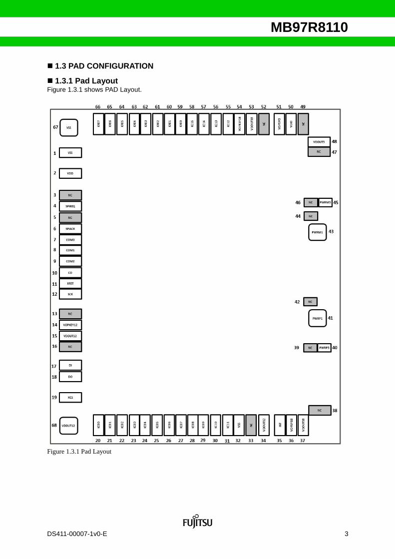
1.3 PAD CONFIGURATION
1.3.1 Pad Layout Figure 1.3.1 shows PAD Layout.
Figure 1.3.1 Pad Layout

4 DS411-00007-1v0-E
MB97R8110
1.3.2 Pad Information Table1.3.2 shows PAD configuration and Power source. Table 1.3.2 Pad configuration and Power source
Pad Name In / Out Power Source Terminal Function Description1 VSS VSS - - Ground 2 VDD In (Power) - - External power input for SPI Slave communication (3V)3 NC - - - Open4 SPIREQ In VOPSPI3 Pull Down(1MΩ) SPI Slave request input5 NC - - - Open6 SPIACK Out VOPSPI3 - Response to SPI Slave resuest (SPI Status output)7 COM0 Out VOPSPI3 - GPIO(register data output)8 COM1 Out VOPSPI3 - GPIO(register data output)9 COM2 Out VOPSPI3 - GPIO(register data output)
10 CD Out VOPSPI3 - Command/Data output11 XRST Out VOPSPI3 - Reset output12 SCK In/Out VOPSPI3 - SPI Clock13 NC - - - Open14 VOPKEY12 In (Power) - Pull Down(6MΩ) Power input for Key Matrix scan circuit (connect to pad15)15 VDOUT12 Out (Power) - - Internally generated power output(1.2V)16 NC - - - Open17 DI In VOPSPI3 - SPI Data input18 DO Out VOPSPI3 - SPI Data output19 XCS In/Out VOPSPI3 - SPI Chip select20 KC00 Out VOPKEY18 - Key Matrix scan pulse output21 KC01 Out VOPKEY18 - Key Matrix scan pulse output22 KC02 Out VOPKEY18 - Key Matrix scan pulse output23 KC03 Out VOPKEY18 - Key Matrix scan pulse output24 KC04 Out VOPKEY18 - Key Matrix scan pulse output25 KC05 Out VOPKEY18 - Key Matrix scan pulse output26 KC06 Out VOPKEY18 - Key Matrix scan pulse output27 KC07 Out VOPKEY18 - Key Matrix scan pulse output28 KC08 Out VOPKEY18 - Key Matrix scan pulse output29 KC09 Out VOPKEY18 - Key Matrix scan pulse output30 KC10 Out VOPKEY18 - Key Matrix scan pulse output31 KC11 Out VOPKEY18 - Key Matrix scan pulse output32 VSS VSS - -33 NC - - - Open34 VDOUT12 Out (Power) - - Internally generated power output (for Internal circuit)35 INT In - - GPIO(register data input)36 VOPSPI18 In (Power) - Pull Down(6MΩ) Power input for SPI and GPIO (connect to pada37)37 VDOUT18 Out (Power) - - Internally generated power output(for FRAM)38 NC - - - Open39 NC - - - Open40 PWRP3 In - - Antenna pad for external power supply41 PWRP1 In - - Antenna pad for RF communication42 NC - - - Open43 PWRM1 In - - Antenna pad for RF communication44 NC - - - Open45 PWRM3 In - - Antenna pad for external power supply46 NC - - - Open47 NC - - - Open48 VDOUT3 Out (Power) - - Power output for external devices49 NC - - - Open50 VDIO Out (Power) - - IO Power output51 VOPSPI3 In (Power) VOPSPI3 Pull Down(6MΩ) Power input for SPI and GPIO (connect to Pad50)52 NC - - - Open53 VDOUT18 Out (Power) - - Internally generated power output(for FRAM)54 VOPKEY18 In (Power) VOPKEY18 Pull Down(6MΩ) Power input for Key Matrix scan circuit (connect to pad53)55 KC12 Out VOPKEY18 - Key Matrix scan pulse output56 KC13 Out VOPKEY18 - Key Matrix scan pulse output57 KC14 Out VOPKEY18 - Key Matrix scan pulse output58 KC15 Out VOPKEY18 - Key Matrix scan pulse output59 KR00 In VOPKEY18 Pull Down(150kΩ) Key Matrix scan data input60 KR01 In VOPKEY18 Pull Down(150kΩ) Key Matrix scan data input61 KR02 In VOPKEY18 Pull Down(150kΩ) Key Matrix scan data input62 KR03 In VOPKEY18 Pull Down(150kΩ) Key Matrix scan data input63 KR04 In VOPKEY18 Pull Down(150kΩ) Key Matrix scan data input64 KR05 In VOPKEY18 Pull Down(150kΩ) Key Matrix scan data input65 KR06 In VOPKEY18 Pull Down(150kΩ) Key Matrix scan data input66 KR07 In VOPKEY18 Pull Down(150kΩ) Key Matrix scan data input67 VSS VSS - -68 VDOUT12 Out (Power) - - Internally generated power output (for Internal circuit)

DS411-00007-1v0-E 5
MB97R8110
1.4 POWER SUPPLY This operational power is internally generated from RF power. For extended feature other than RFID tag feature, such as SPI Master, SPI Slave, and Key Matrix scan, the optional power (VOPSPI3, VOPSPI18, VOPKEY18, VOPKEY12) will be provided by connecting the designated pads as shown in Table1.4. Table 1.4 Power generation
Extended Feature Internal generated Power
(Output pad)
Optional Power
(Input pad)
SPI Master 50 VDIO 51 VOPSPI3
37 VDOUT18 36 VOPSPI18
SPI Slave 50 VDIO 51 VOPSPI3
37 VDOUT18 36 VOPSPI18
Key Matrix Scan 15 VDOUT12 14 VOPKEY12
53 VDOUT18 54 VOPKEY18

6 DS411-00007-1v0-E
MB97R8110
2 RF INTERFACE RF signal interface is compliant with EPCglobal Class 1 Generation 2 Ver.1.2.0.
2.1 Modulation type, communications timing Compliant with EPCglobal Class 1 Generation 2 Ver.1.2.0
2.2 Inventory, Tag selection Compliant with EPCglobal Class 1 Generation 2 Ver.1.2.0
2.3 Tag state-transition Compliant with EPCglobal Class 1 Generation 2 Ver.1.2.0
2.4 RF communication Error code This LSI replies error code if it encounters an error when executing a handle-based command under Open state or Secured state. Error code described in EPCglobal Class 1 Generation 2 Ver.1.2.0 (AnnexI) and a proprietary error code are supported as shown in Table2.4. Table 2.4 Error code
※1. This error covers not only RF command operation but also extended application (refer to Chapter 7). If the power is insufficient to backscatter, the LSI cannot reply error code, ※2. Proprietary Error code for Key Matrix scan application
Error code Error code name Error description
00h Other errors Other errors not covered by the following errors
03h Memory overrun The specified memory location does not exist.
04h Memory locked The specified memory location is locked or permalocked
0Bh Insufficient power Insufficient power to perform the operation ※1
8Eh No detection of Keys ※2 No pressed key detected during the Key Matrix scan operation

DS411-00007-1v0-E 7
MB97R8110
3 SPI Interface
3.1 Overview This LSI has SPI (Serial Peripheral Interface) interface that enables to operate the following features. ・As SPI slave device, the memory data can be accessed through the SPI interface (External power is required for the operation). ・As SPI master device, the external SPI slave device can be controlled by RF command (RF generated power is
supplied for the external device).
3.2 SPI Mode This LSI supports SPI mode 0 (CPOL=0, CPHA=0).
Figure 3.2 – SPI mode
3.3 SPI Slave Interface
3.3.1 Connection to SPI Interface When this LSI is used as SPI slave device, the connection with SPI controller (master) shall be as shown in Figure 3.3.1. In order to start SPI slave communication, SPI controller shall set SPIREQ to “H” level to request the communication. After SPIACK outputs “H” level, XCS shall be set to “L” level. And then SPI slave communication will be enabled. SPI controller shall stay SPIREQ “H” level, and can continue to execute commands without any interruption from RF interface during when SPIACK is “H” level. Any command from RF interface is invalid during SPI slave operation. When SPIACK is “L” level, SPI slave communication cannot be enabled.
Figure 3.3.1 - SPI Slave interface connection

8 DS411-00007-1v0-E
MB97R8110
3.3.2 Power down mode This LSI implements Power down mode if SPIREQ is switched to “L” level, which enables to reduce current consumption of the battery connected between VDD-VSS. (refer to 8.4.1) When the voltage is applied on VDD, and SPIREQ=”L” level without RF carrier, the output of both SPIACK and DO becomes undefined, it is recommended for controller to deactivate the signal to SPIACK and DO. All the control pin (including XCS) excepting VDD must be “L” level in power down mode.
3.3.3 Usage Please refer to Chapter 5.2 and 5.3.regarding the usage of SPI slave interface.
3.4 SPI Master Interface
3.4.1 Connection to SPI Interface When this LSI is used as SPI master device, the connection with SPI slave device shall be as shown in Figure 3.4.1.1 and Figure 3.4.1.2. It is recommended to connect capacitor between VDOUT3 and VSS, when SPI slave device operation causes rapid current consumption. And power supply to SPI slave device is recommended to be controlled by “H” level output from any bit out of COM[2:0] of GPIO (refer to Chapter 7.2.1). VDIO output shall be connected to VOPSPI3, and VDOUT18 output shall be connected to VOPSPI18. In this case “H” level output of COM[2:0] will be the same as the voltage level input from VOPSPI3. Figure 3.4.1.1 shows an example of SPI master interface connection, in which XRST and CD pins are used for the connection. And DI and DO are connected with SPI slave device respectively. Busy signal of SPI slave device is connected to INT pin, which is assigned in GPIO interface, and busy status can be read by Reader/Writer (refer to 7.2.2). Figure 3.4.1.2 shows another example of SPI master interface connection, in which XRST, CD, and INT pins are not used for the connection. And DI and DO is used as common bus connection (Mux).
Figure 3.4.1.1 - SPI master interface connection 1 Figure 3.4.1.2 - SPI master interface connection 2
3.4.2 Usage Please refer to Chapter 7.1 regarding the usage of SPI master interface.

DS411-00007-1v0-E 9
MB97R8110
3.5 GPIO Interface
3.5.1 GPIO GPIO interface enables to output 3bits of register value to COM[2:0] pins (refer to chapter 4.2.4.2 about address allocation). The value can be updated by BlockWrite command of RF communication. The state of INT can be read by Read command of RF communication.
3.5.2 Usage GPIO can be utilized as the following use cases. ・ LED ON/OFF control ・ Power supply to SPI slave device under SPI master operation ・ Status monitoring of external connected devices For the detail, refer to Chapter 7.2.

10 DS411-00007-1v0-E
MB97R8110
3.6 Key Matrix scan interface
3.6.1 Connection method The Key Matrix scan interface enables to be connected to matrix key input device which returns key data on scan clock.
Figure 3.6.1 – Key Matrix and connection example
3.6.2 Usage Refer to Chapter 7.3 regarding the usage of Key Matrix scan interface
DS411-00007-1v0-E 11
MB97R8110
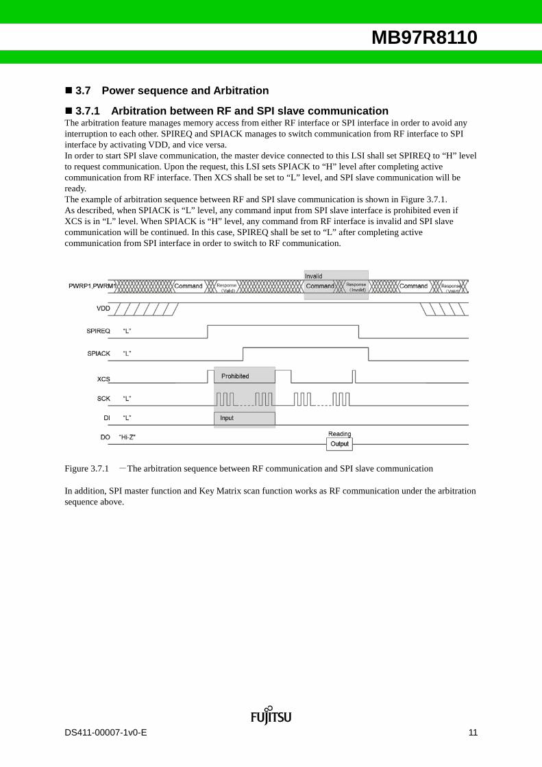
3.7 Power sequence and Arbitration
3.7.1 Arbitration between RF and SPI slave communication The arbitration feature manages memory access from either RF interface or SPI interface in order to avoid any interruption to each other. SPIREQ and SPIACK manages to switch communication from RF interface to SPI interface by activating VDD, and vice versa. In order to start SPI slave communication, the master device connected to this LSI shall set SPIREQ to “H” level to request communication. Upon the request, this LSI sets SPIACK to “H” level after completing active communication from RF interface. Then XCS shall be set to “L” level, and SPI slave communication will be ready. The example of arbitration sequence between RF and SPI slave communication is shown in Figure 3.7.1. As described, when SPIACK is “L” level, any command input from SPI slave interface is prohibited even if XCS is in “L” level. When SPIACK is “H” level, any command from RF interface is invalid and SPI slave communication will be continued. In this case, SPIREQ shall be set to “L” after completing active communication from SPI interface in order to switch to RF communication.
Figure 3.7.1 -The arbitration sequence between RF communication and SPI slave communication In addition, SPI master function and Key Matrix scan function works as RF communication under the arbitration sequence above.

12 DS411-00007-1v0-E
MB97R8110
4 Memory
4.1 Memory address
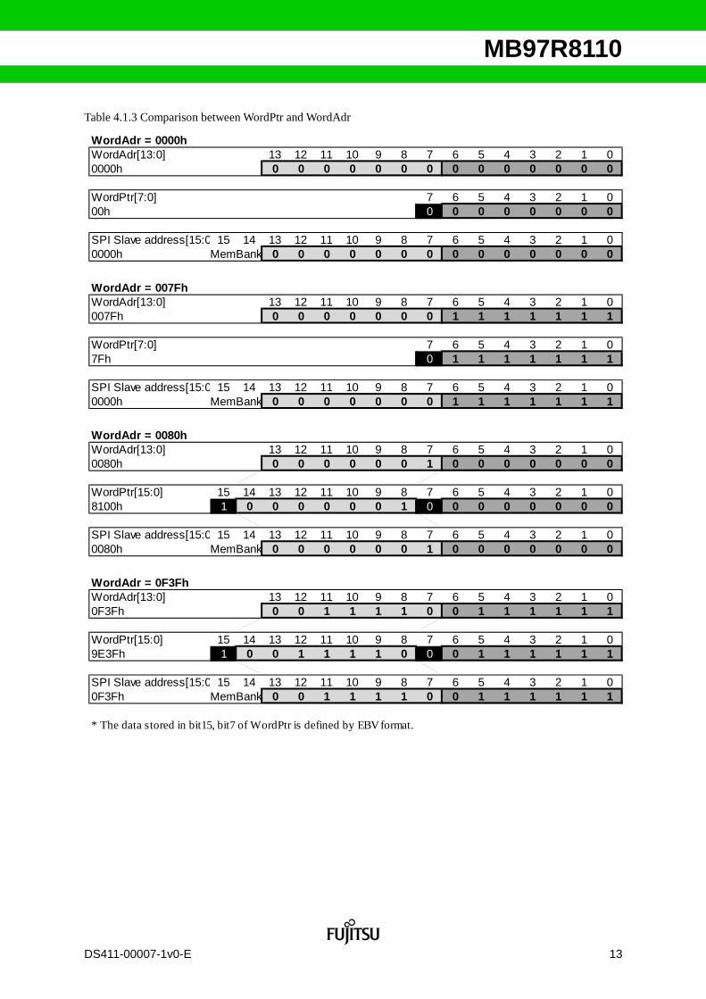
4.1.1 Address description The memory address is allocated in the units of 16bits (=1word). The logical address in each memory bank is described as WordAdr in this document. WordPtr is the address specified by RF command access, which is described in EBV(Extensible bit vectors) format conforming to EPCglobal Class 1 Generation 2 standard (AnnexA). EBV format is shown in Talbe4.1.1. The address description in this document is shown in Table4.1.2. And the practical examples of the comparison between WordPtr and WordAdr are shown in Table4.1.3. Table 4.1.1 EBV format (Excerpt from EPCglobal standard)
Table 4.1.2 Address description in this document
Address range WordAdr[13:0] *1
WordPtr[7:0] or WordPtr[15:8] (RF access)
Comparison between WordPtr and WordAdr
0000h to 007Fh 0000h to 007Fh 00h to 7Fh WordPtr={0, WordAdr[6:0]} *2
0080h to 3FFFh 0080h to 3FFFh 8100h to FF7Fh WordPtr={1,WordAdr[13:7], 0,WordAdr[6:0]} *2
*1. The address specified by SPI slave access is 2bits of MemBank and 14bits of WordAdr (16bits total). *2. Underlined 0,1 is defined by EBV format.
DS411-00007-1v0-E 13
MB97R8110
Table 4.1.3 Comparison between WordPtr and WordAdr
WordAdr = 0000hWordAdr[13:0] 13 12 11 10 9 8 7 6 5 4 3 2 1 00000h 0 0 0 0 0 0 0 0 0 0 0 0 0 0
WordPtr[7:0] 7 6 5 4 3 2 1 000h 0 0 0 0 0 0 0 0
SPI Slave address[15:0 15 14 13 12 11 10 9 8 7 6 5 4 3 2 1 00000h 0 0 0 0 0 0 0 0 0 0 0 0 0 0
WordAdr = 007FhWordAdr[13:0] 13 12 11 10 9 8 7 6 5 4 3 2 1 0007Fh 0 0 0 0 0 0 0 1 1 1 1 1 1 1
WordPtr[7:0] 7 6 5 4 3 2 1 07Fh 0 1 1 1 1 1 1 1
SPI Slave address[15:0 15 14 13 12 11 10 9 8 7 6 5 4 3 2 1 00000h 0 0 0 0 0 0 0 1 1 1 1 1 1 1
WordAdr = 0080hWordAdr[13:0] 13 12 11 10 9 8 7 6 5 4 3 2 1 00080h 0 0 0 0 0 0 1 0 0 0 0 0 0 0
WordPtr[15:0] 15 14 13 12 11 10 9 8 7 6 5 4 3 2 1 08100h 1 0 0 0 0 0 0 1 0 0 0 0 0 0 0 0
SPI Slave address[15:0 15 14 13 12 11 10 9 8 7 6 5 4 3 2 1 00080h 0 0 0 0 0 0 1 0 0 0 0 0 0 0
WordAdr = 0F3FhWordAdr[13:0] 13 12 11 10 9 8 7 6 5 4 3 2 1 00F3Fh 0 0 1 1 1 1 0 0 1 1 1 1 1 1
WordPtr[15:0] 15 14 13 12 11 10 9 8 7 6 5 4 3 2 1 09E3Fh 1 0 0 1 1 1 1 0 0 0 1 1 1 1 1 1
SPI Slave address[15:0 15 14 13 12 11 10 9 8 7 6 5 4 3 2 1 00F3Fh 0 0 1 1 1 1 0 0 1 1 1 1 1 1
* The data stored in bit15, bit7 of WordPtr is defined by EBV format.
MemBank
MemBank
MemBank
MemBank

14 DS411-00007-1v0-E
MB97R8110
4.2 Memory Map
4.2.1 Memory bank The Non-volatile memory (FRAM) of this LSI is divided into the following four banks. Table 4.2.1 Memory map
MemBank[1:0]
Definition WordAdr[13:0] WordPtr[15:8]
WordPtr[7:0]
Read
Write
BlockW
rite
BlockE
rase
BlockP
ermalock
Select
SpiR
ead
SpiW
rite
0000h to 0EFFh 00h to 9D7Fh ✔ ✔ ✔ ✔ ✔ ✔ ✔ ✔0F00h to 0F3Fh 9E00h to 9E3Fh ✔ - ✔* ✔* - ✔ ✔ -
10 TID 0000h to 000Ch 00h to 0Ch ✔ - - - - ✔ ✔ -
01 EPC 0000h to 001Fh 00h to 1Fh ✔ ✔ ✔ ✔ - ✔ ✔ -
00 RESERVED 0000h to 003Fh 00h to 3Fh ✔ ✔ - - - - - -
*. The command works for executing extended application on some specific address.
11 USER
Address
RF
Command AccessibilityBank
SPI Slave
USER, TID, EPC, and RESERVED memory banks contain the data in the format defined by EPCglobal C1G2 specification (Chapter 6.3.2.1). In each memory bank, the WordAdr and the WordPtr start from zero (00h).
4.2.2 TID bank The memory map of TID bank is shown in Table 4.2.2. TID bank can only be read, and the setting values cannot be changed. For details, please refer to EPCglobal Class 1 Generation 2 standard. Table 4.2.2 TID bank memory map
MSB LSB
WordAdr WordPtr 15 14 13 12 11 10 9 8 7 6 5 4 3 2 1 0 SettingValue
00h 00h E281h01h 01h 0081h02h 02h 3C00h03h 03h unique04h 04h unique05h 05h unique06h 06h 1DDEh07h 07h 0002h08h 08h 0310h09h 09h 0002h0Ah 0Ah 0310h0Bh 0Bh 0200h0Ch 0Ch 0F00hUser memory size
BlockWrite parameterBlockWrite parameterPermalock Block size
BlockErase parameter
Allocation ClassDesigner
DesignerProduct ID Version
BlockErase parameter
XTID headerSerial NumberSerial NumberSerial Number
optional command support

DS411-00007-1v0-E 15
MB97R8110
4.2.3 EPC bank The memory map of EPC bank is shown in Table 4.2.3. Table 4.2.3 EPC bank memory map
MSB LSB
WordAdr WordPtr 15 14 13 12 11 10 9 8 7 6 5 4 3 2 1 0 DefaultValue
00h 00h01h 01h 3400h02h 02h 0000h03h 03h unique04h 04h unique05h 05h unique06h 06h 0000h07h 07h 0000h08h 08h 0000h09h 09h 0000h0Ah 0Ah 0000h0Bh 0Bh 0000h0Ch 0Ch 0000h0Dh 0Dh 0000h0Eh 0Eh 0000h0Fh 0Fh 0000h10h 10h 0000h・・・ ・・・ 0000h1Fh 1Fh 0000h*. As default value, the same serial number is stored in WordAdr=03h to 05h of EPC bank as thenumber stored in WordAdr=03h to 05h of TID bank.
EPC data
EPC dataEPC data(Serial Number *)EPC data(Serial Number *)EPC data(Serial Number *)
EPC dataEPC data
EPC dataEPC dataEPC data
EPC data
EPC dataEPC dataEPC dataEPC dataEPC dataEPC data
Stored CRCStored PC
The length of EPC is specified by EPC length field of Stored PC. The length is preprogrammed to 6 (words) as default value, which indicates 6words of EPC (WordAdr 02h to 07h). It is possible to expand the length up to 30words (WordAdr 02h to 1Fh) by programming the data of EPC length field This LSI does not support XPC_W1 and XPC_W2. Stored CRC is not preprogrammed, because it is reflected after the response to ACK command.

16 DS411-00007-1v0-E
MB97R8110
4.2.4 USER bank USER bank of this LSI consists of 3,840words of Data field and 64words of Application field.
4.2.4.1 USER bank (Data field) Data field of USER bank is divided into 8 Area groups as shown in Table.4.2.4.1. Table 4.2.4.1 USER bank (Data field) memory map
MSB LSB
WordAdr WordPtr 15 14 13 12 11 10 9 8 7 6 5 4 3 2 1 0 DefaultValue
000h to 1FFh 00h to 837Fh 0000h200h to 3FFh 8400h to 877Fh 0000h400h to 5FFh 8800h to 8B7Fh 0000h600h to 7FFh 8C00h to 8F7Fh 0000h800h to 9FFh 9000h to 937Fh 0000hA00h to BFFh 9400h to 977Fh 0000hC00h to DFFh 9800h to 9B7Fh 0000hE00h to EFFh 9C00h to 9D7Fh 0000h
User data (Area5)User data (Area6)User data (Area7)
User data (Area0)User data (Area1)User data (Area2)User data (Area3)User data (Area4)
Each area can be protected by Area Password (refer to Chapter6.2). And the same area is allocated for PermalockBlock (refer to Chapter5.1.3). Regarding the memory access from RF communication (BlockWrite, BlockErase, and Read command), when the address reaches to WordPtr=8F7Fh (WordAdr=7FFh) among the range specified by WordCount, the address to be followed will be WordPtr=9000h (WordAdr=800h). In the same case from SPI slave communication (SpiWrite, SpiRead command), the address counter rollovers from WordAdr=7FFh to 000h.
4.2.4.2 USER bank (Application field) Application field of USER bank allocated in WordPtr=9E00h to 9E3Fh (WordAdr=F00h to F3Fh) is used for the extensive applications described in Chapter 7, and consists of 16bits of volatile registers. This field is writable only from RF interface. The stored value will be reset to “0”, if the internal voltage drops below the lower limit. Memory map of the field is shown in Table.4.2.4.2. Table 4.2.4.2 USER bank (Application field) memory map
MSB LSB
WordAdr WordPtr 15 14 13 12 11 10 9 8 7 6 5 4 3 2 1 0 ResetValue
F00h 9E00h 0000hF01h 9E01h 0000hF02h 9E02h 0000hF03h 9E03h 0000hF04h 9E04h 0000hF05h 9E05h 0000h・・・ ・・・ 0000hF0Fh 9E0Fh 0000hF10h 9E10h 0000hF11h 9E11h 0000hF12h 9E12h 0000hF13h 9E13h 0000hF14h 9E14h 0000h・・・ ・・・ 0000hF1Fh 9E1Fh 0000hF2xh 9E2xh 0000hF3xh 9E3xh 0000h
GPIO SettingKey Matrix scan setting
SPI Master setting
RFURFU
RFUVDOUT3 setting
RFU
Pressed Key data bufferKey Matrix scan command control and Pressed Key data buffer
Pressed Key data buffer
SPI Master command controlSPI Masetr command control and response buffer
ReservedReservedReserved
Pressed Key data buffer

DS411-00007-1v0-E 17
MB97R8110
4.2.5 RESERVED bank RESERVED bank is used for Password data management. 32bits Password can be set by 2steps of 16bits writing, 1st for [31:16] and 2nd for [15:0] by Req_RN and Write command as a set of sequence respectively without any other command between the steps. Table 4.2.5 RESERVED bank memory map
MSB LSB
WordAdr WordPtr 15 14 13 12 11 10 9 8 7 6 5 4 3 2 1 0 DefaultValue
00h 00h Kill password [31:16] 0000h01h 01h Kill password [15:0] 0000h02h 02h Access password [31:16] 0000h03h 03h Access password [15:0] 0000h04h 04h 0000h・・・ ・・・ 0000h1Fh 1Fh 0000h20h 20h Area password(Setting) (Area0) [31:16] 0000h21h 21h Area password(Setting) (Area0) [15:0] 0000h22h 22h Area password(Setting) (Area1) [31:16] 0000h23h 23h Area password(Setting) (Area1) [15:0] 0000h24h 24h Area password(Setting) (Area2) [31:16] 0000h25h 25h Area password(Setting) (Area2) [15:0] 0000h26h 26h Area password(Setting) (Area3) [31:16] 0000h27h 27h Area password(Setting) (Area3) [15:0] 0000h28h 28h Area password(Setting) (Area4) [31:16] 0000h29h 29h Area password(Setting) (Area4) [15:0] 0000h2Ah 2Ah Area password(Setting) (Area5) [31:16] 0000h2Bh 2Bh Area password(Setting) (Area5) [15:0] 0000h2Ch 2Ch Area password(Setting) (Area6) [31:16] 0000h2Dh 2Dh Area password(Setting) (Area6) [15:0] 0000h2Eh 2Eh Area password(Setting) (Area7) [31:16] 0000h2Fh 2Fh Area password(Setting) (Area7) [15:0] 0000h30h 30h Area password(Authentication) (Area0) [31:16] 0000h31h 31h Area password(Authentication) (Area0) [15:0] 0000h32h 32h Area password(Authentication) (Area1) [31:16] 0000h33h 33h Area password(Authentication) (Area1) [15:0] 0000h34h 34h Area password(Authentication) (Area2) [31:16] 0000h35h 35h Area password(Authentication) (Area2) [15:0] 0000h36h 36h Area password(Authentication) (Area3) [31:16] 0000h37h 37h Area password(Authentication) (Area3) [15:0] 0000h38h 38h Area password(Authentication) (Area4) [31:16] 0000h39h 39h Area password(Authentication) (Area4) [15:0] 0000h3Ah 3Ah Area password(Authentication) (Area5) [31:16] 0000h3Bh 3Bh Area password(Authentication) (Area5) [15:0] 0000h3Ch 3Ch Area password(Authentication) (Area6) [31:16] 0000h3Dh 3Dh Area password(Authentication) (Area6) [15:0] 0000h3Eh 3Eh Area password(Authentication) (Area7) [31:16] 0000h3Fh 3Fh Area password(Authentication) (Area7) [15:0] 0000h
Reserved
Reserved

18 DS411-00007-1v0-E
MB97R8110
5 Command (Battery-less operation)
5.1 RF communication command All mandatory commands and optional commands specified in EPCglobal C1G2 Ver.1.2.0. (Chapter 6.3.2.11) are supported as described in Table 5.1. However, Parts of the specification of BlockWrite, BlockErase, BlockPermalock command (Optional command), and Read command (Mandatory command) are different form EPC C1G2 standard as described in Chapter 5.1.1,5.1.2, 5.1.3, and 5.1.4. Table 5.1 – RF mode command Type Command name Command code
Mandatory QueryRep 00
ACK 01
Query 1000
QueryAdjust 1001
Select 1010
NAK 1100 0000
Req_RN 1100 0001
Read 1100 0010
Write 1100 0011
Kill 1100 0100
Lock 1100 0101
Optional Access 1100 0110
BlockWrite 1100 0111
BlockErase 1100 1000
BlockPermalock 1100 1001
※Differences from EPCglobal C1G2 Ver. 1.2.0 (1) Stored CRC-16 If Stored PC and/or EPC data stored in EPC bank are renewed, StoredCRC-16 will not be updated when the power is turned on, but it is updated on the response to ACK command without truncation. (2)UMI UMI is fixed to “1” on this LSI. According to EPCglobal C1G2 Ver. 1.2.0, UMI stored in bit[10] of StoredPC in EPC bank shall be calculated by OR of bit[12:8] of WordAdr=00h in USER bank. (3)Response to Read command when the WordCount is specified to 00h According to EPCglobal C1G2 Ver. 1.2.0, the tag shall reply the whole data from the specified WordPtr to the last address of the bank, when the WordCount is specified to 00h. USER bank of this LSI consists of 8 areas and can be protected by Area Password. Therefore, if parts of the data to be read is protected by Area Password, any data cannot be read and error code “04h” (indicating Memory locked) will be replied. (4)Commands for extended applications As described in Chapter 7, BlockWrite and BlockErase commands are used for executing extended application when the commands access to the specific address allocated in WordPtr=9E00h to 9E3Fh (WordAdr=F00h to F3Fh) of USER bank. In this case, these commands do not work as simple Write and Erase command. (5)Area Password Area Password for data protection is stored in WordPtr=20h to 3Fh (WordAdr=20h to 3Fh) of RESERVED bank. As described in Chapter 6, Write command is used for Area Password setting and authentication when the command accesses to the specific address.

DS411-00007-1v0-E 19
MB97R8110
5.1.1 BlockWrite (Optional command) BlockWrite command format is shown in Table5.1.1. Part of the function are different from what is specified in EPCglobal C1G2 Ver.1.2.0 as following. ・MemBank specifies only EPC and USER bank. If BlockWrite command is executed on RESERVED and TID bank, error code “03h” (indicating Memory overrun) is replied. In this case, the data will not be written into the specified address. ・WordCount specifies the number of words to be written. If 00h is specified, the command will be ignored. When the specified address is located in EPC bank or some address located in WordPtr=00h to 9D7Fh (WordAdr=000h to 7FFh) of USER bank, WordCount shall be 16(10h) or less. If it is 17(11h) or more, error code “03h” (indicating Memory overrun) will be replied. When the specified address is located in WordPtr=9E00h to 9E3Fh (WordAdr=800h to EFFh), WordCount shall be specified up to 255(FFh). In this case, the data up to 16words is to be written into the specified address after CRC verification, but the data over 16words is to be written continuously without CRC verification. Therefore if the communication is terminated without any response because of low power detection, some data may have been written before the termination. When the specified address is all or partially locked by the BlockPermalock command or protected by Area Password, any data will not be written and error code “04h” (indicating Memory locked) is replied. Table 5.1.1 - BlockWrite command
Command MemBank WordPtr WordCount Data RN CRC
Number of bits 8 2 EBV 8 WordCount *16 16 16
Description 1100 0111 01:EPC 11:USER
Starting Address Pointer
Number of words to
write
Data to be written
handle CRC-16
When the address reaches WordPtr=8F7Fh (WordAdr=7FFh) among the range specified by WordCount, the address to be followed will be WordPtr=9000h (WordAdr=800h). * In SPI slave communication, the address counter rollovers from WordAdr=7FFh to 000h.
5.1.2 BlockErase (Optional command) BlockErase command format is shown in Table5.1.2. Parts of the function are different from what is specified in EPCglobal C1G2 Ver.1.2.0 as described as follows. ・MemBank specifies only EPC and USER bank. If BlockErase command is executed on RESERVED and TID bank, error code “03h” (indicating Memory overrun) is replied. In this case, the data will not be erased. ・WordCount specifies the number of data to be erased. If 00h is specified, the command will be ignored. 01h to 10h shall be specified. When the specified address is all or partially locked by the BlockPermalock command or protected by Area Password, any data will not be erased and error code “04h” (indicating Memory locked) is replied. Table 5.1.2 - BlockErase Command
Command MemBank WordPtr WordCount RN CRC
Number of bits 8 2 EBV 8 16 16
Decription 1100 1000 01:EPC 11:USER
Starting Address Pointer
Number of words to
erase
handle CRC-16

20 DS411-00007-1v0-E
MB97R8110
5.1.3 BlockPermalock (Optional command) The unit of Block to be locked is defined as 512 words for this LSI. The BlockPermalock command can be executed to the 8 blocks of USER bank which is 7 areas of 8k bits and 1 area of 4k bits.
5.1.3.1 BlockPermalock (Setting) The format of the BlockPermalock command for Permalock setting is shown in Table 5.1.3.1. The Read/Lock value is set to “1”, and the specified bock will be locked permanently. Lock data field is described in Chapter 5.1.3.3. Table 5.1.3.1 – BlockPermalock command (Permalock)
Command RFU Read /Lock
Mem Bank BlockPtr Block
Range LockData RN CRC
Number of bits 8 8 1 2 8 8 16 16 16
Description 1100 1001 0000 0000
1:Perma Lock
11:USER 0000 0000
0000 0001
0:Retain current
permalock setting
1:Assert permalock
handle CRC-16
There is a limitation as follows. If any other value is set, error code “03h” (indicating Memory overrun) will be replied and permalock operation is terminated. • MemBank: Only executed for USER bank. • BlockPtr: Only 00h is supported. • BlockRange: Only 01h is supported.
5.1.3.2 BlockPermalock (Read) The format of the BlockPermaLock command for reading permalock status is shown in Table 5.1.3.2.1. The Read/Lock value is set to “0”, and the permalock status of 8blocks of USER bank can be read. The response is shown in Table 5.1.3.2.2. Table 5.1.3.2.1 – BlockPermalock command (Read)
Command RFU Read /Lock MemBank BlockPtr Block
Range RN CRC
Number of bits 8 8 1 2 8 8 16 16
Description 1100 1001 00000000
0:Read 11:USER 0000 0000
0000 0001
handle CRC-16
Table 5.1.3.2.2 – Response to BlockPermalock command (Read)
Header LockData RN CRC
Number of bits 1 16 16 16
Description 0 Permalock bits
handle CRC-16

DS411-00007-1v0-E 21
MB97R8110
There is a limitation as follows. If any other value is set, error code “03h” (indicating Memory overrun) will be replied and reading operation is terminated. • MemBank: Only executed for USER bank. • BlockPtr: Only 00h is supported. • BlockRange: Only 01h is supported.
5.1.3.3 BlockPermalock and Permalocked Block 16bits of Lock data and corresponded block is shown in Table 5.1.3.3. Table 5.1.3.3 – BlockPermalock data
Bit Area WordAdr WordPtr
15 0 000h to 1FFh 00h to 837Fh
14 1 200h to 3FFh 8400h to 877Fh
13 2 400h to 5FFh 8800h to 8B7Fh
12 3 600h to 7FFh 8C00h to 8F7Fh
11 4 800h to 9FFh 9000h to 937Fh
10 5 A00h to BFFh 9400h to 977Fh
9 6 C00h to DFFh 9800h to 9B7Fh
8 7 E00h to EFFh 9C00h to 9D7Fh
7 - - -
6 - - -
5 - - -
4 - - -
3 - - -
2 - - -
1 - - -
0 - - -
When Lock data is set by BlockPermalock command (refer to Chapter 5.1.3.1), Bit[7:0] shall be set to “0” because of no target block.

22 DS411-00007-1v0-E
MB97R8110
5.1.4 Read (Mandatory) The command format is shown in Table 5.1.4.1 Table 5.1.4.1– Read command
Command MemBank WordPtr WordCount RN CRC
Number of bits 8 2 EBV 8 16 16
Description 1100 0010 00:RESERVED 01:EPC 10:TID 11:USER
Starting Address Pointer
Number of Words to
read
handle CRC-16
When the address reaches WordPtr=8F7Fh (WordAdr=7FFh) among the range specified by WordCount, the address to be followed will be WordPtr=9000h (WordAdr=800h). * In SPI slave communication, the address counter rollovers from WordAdr=7FFh to 000h. When WordCount is set to “00h”, the response will be as shown in Table 5.1.4.2. Table 5.1.4.2– Response to Read command when WordCount is set to “00h”
MemBank Area Password Response
11:USER Zero Password (All Area)
The data from the specified WordPtr (Table 5.1.4.1) to 9D7Fh (WordAdr=EFFh) are replied as normal response.
Non zero Password (Some Area)
No data is read. Error code “04h” (indicating Memory locked) is replied. (refer to Chapter 2.4)
10:TID - The data from the specified WordPtr (Table 5.1.4.1) to 0Fh are replied as normal response.
01:EPC - The data from the specified WordPtr (Table 5.1.4.1) to the WordPtr corresponding to the length of EPC are replied as normal response.
00:RESERVED - The data from the specified WordPtr (Table 5.1.4.1) to 3Fh are replied as normal response.
DS411-00007-1v0-E 23
MB97R8110
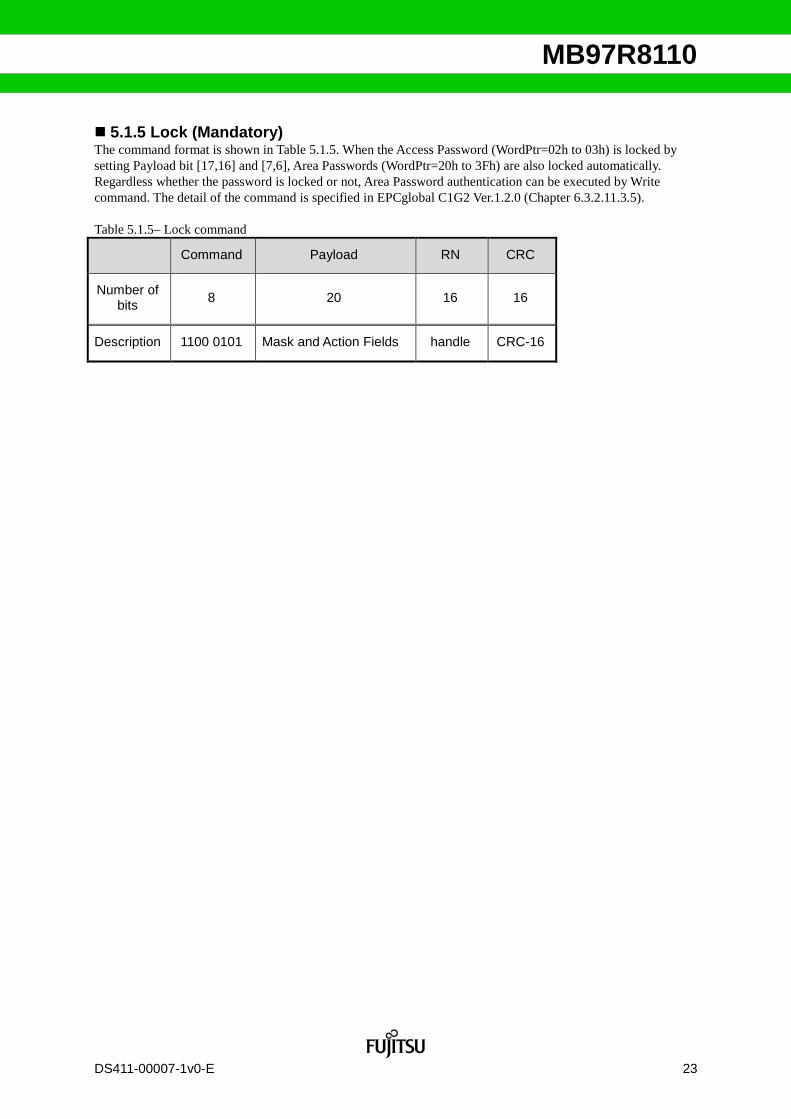
5.1.5 Lock (Mandatory) The command format is shown in Table 5.1.5. When the Access Password (WordPtr=02h to 03h) is locked by setting Payload bit [17,16] and [7,6], Area Passwords (WordPtr=20h to 3Fh) are also locked automatically. Regardless whether the password is locked or not, Area Password authentication can be executed by Write command. The detail of the command is specified in EPCglobal C1G2 Ver.1.2.0 (Chapter 6.3.2.11.3.5). Table 5.1.5– Lock command
Command Payload RN CRC
Number of bits 8 20 16 16
Description 1100 0101 Mask and Action Fields handle CRC-16

24 DS411-00007-1v0-E
MB97R8110
5.2 SPI slave communication command This LSI will support 3 types of operate-code for SPI slave interface. The operate-code is 8bits code described in Table 5.2. If other codes are used, the command is ignored. If XCS is raised during the input sequence of operate-code, the command cannot be executed. Table 5.2 - Operate-code for SPI slave interface
Code name Function Operate-code
SpiRead Read data in units of 16bits from USER memory area. 0000 0011 SpiWrite Write data in units of 16bits into USER memory area. 0000 0010 SpiRDSR Read 16bits of Error information register(SPI slave) 0000 0101
5.2.1 SpiRead SpiRead command is to read memory data in units of 16bits (1word). The address shall be specified as 2bits of MemBank followed by 14bits of WordAdr (Total 16bits). The command sequence is described in Figure 5.2.1. Through DI pin, the following data shall be input synchronously to the rising edge of SCK after XCS is fallen. SpiRead operate code (8bit:03h) MemBank (2bit) WordAdr (14bit) USER bank, TID bank and EPC bank are readable banks. The upper 2 bit of WordAdr shall be fixed to “00”. In response to the command input, the reading data will be output from DO synchronously to the falling edge of SCK. During the period of output form DO, any input from DI will be ignored. SpiRead command will be terminated when XCS is raised, and the output from DO will be “Hi-Z”. The command keeps on reading with automatically incremented address by continuous 16cycles of clock to SCK before XCS rising. If WordAdr is specified as 000h to 7FFh of USER bank and the incremented address reaches to WordAdr=7FFh, the address will roll over to WordAdr=000h and read operation is continued. If WordAdr is specified as 800h to EFFh of USER bank and the incremented address reaches to WordAdr=EFFh, the address will not roll over to WordAdr=000h nor WordAdr=800h. In this case, the DO output will be “0”. When Membank is specified as TID bank or EPC bank, the address will be automatically incremented up to the most significant WordAdr described in Chaper 4.2, and the address will not roll over after that. In this case, the DO output will be “0” until when XCS is raised. In the following cases, the memory data will not be read out and DO output will be “0”. 1) LSI is in Killed state 2) The specified address is protected by Password 3) MemBank is specified with RESERVED bank
Figure 5.2.1 – SpiRead command sequence When AccessPassword is set, the data cannot be read and the output will be “0”. Therefore AccessPassword shall be cleared before SPI slave communication. If the specified area includes the WordAdr protected by Area Password, only unprotected address will be read and “0” will be output instead from protected address.

DS411-00007-1v0-E 25
MB97R8110
5.2.2 SpiWrite SpiWrite command is to write data into memory in units of 16 bits (1 word). The address shall be specified as 2bits of MemBank followed by 14bits WordAdr (Total 16bits). The command sequence is described in Figure 5.2.2. Through DI pin, the following data shall be input synchronously to the rising edge of SCK after XCS is fallen. SpiWrite operate-code (8bit:02h) MemBank (2bit) WordAdr (14bit) Written data (N*16bit) USER bank is writable bank, and the other banks are not writable. The upper 2 bit of WordAdr shall be fixed to “00”. The command keeps on writing with automatically incremented address by continuous 16 cycles of clock to SCK and 16bits of writing data together before XCS rising. If XCS is raised on the timing before completing 16cycles of clock, the writing data will not be written into memory. If WordAdr is specified as 000h to 7FFh of USER bank and the incremented address reaches to WordAdr=7FFh, the address will roll over to WordAdr=000h and write operation is continued. If WordAdr is specified as 800h to EFFh of USER bank and the incremented address reaches to WordAdr=EFFh, the address will not roll over to WordAdr=000h nor WordAdr=800h. In this case, writing operation completes at WordAdr =EFFh. In the following cases, the writing data cannot be written, and error information will be stored into SPI error information. (refer to Chapter 5.3.1 for detail). 1) LSI is in Killed state 2) The specified address is protected by Password 3) The specified MemBank is not USER bank 4) WordAdr is over EFFh 5) The specified address is in the locked area
Figure 5.2.2 – SpiWrite command sequence When AccessPassword is set, the data cannot be written. Therefore AccessPassword shall be cleared before SPI slave communication. If the specified area includes the WordAdr protected by Area Password, only unprotected address will be written and nothing will happen on protected address. If the specified area includes the WordAdr locked by Lock command or BlockPermalock command, only writable address will be written and nothing will happen on locked address for writing.

26 DS411-00007-1v0-E
MB97R8110
5.2.3 SpiRDSR The SpiRDSR command is to read 16 bits of error information on SPI slave communication (refer to Chapter 5.3.1). The command sequence is described in Figure 5.2.3. Through DI pin, the following data shall be input synchronously to the rising edge of SCK after XCS is fallen. SpiRDSR operate-code (8bit:05h) In response to the command input, the 16 bits of error information will be output from DO synchronously to the falling edge of SCK. And SpiRDSR command will be completed when XCS is raised. If XCS is raised before the command completes 16 cycles of clock to SCK, the command will be terminated and the output from DO will be “Hi-Z”. During the period of output from DO, any input from DI will be ignored. If XCS keeps “L” level after the command complete reading, the output from DO will be “L” level. The error information will be cleared after SpiRDSR command is completed.
Figure 5.2.3 – SpiRDSR command sequence

DS411-00007-1v0-E 27
MB97R8110
5.3 Error handling to SPI slave communication On SPI slave communication, an error occurs under the following condition. If an error occurs in SPIRead command operation, the output from DO will be “0” and error information will be stored in error information register. ・Specified memory are is locked. ・Killed status The data stored in error information register can be read by SpiRDSR command.
5.3.1 Error information register (SPI slave communication) Error information during SPI slave communication will be stored in the error information as shown in Table 5.3.1. These information can be read by SpiRDSR command. The information will be cleared after the following operation. ・SpiRDSR command execution ・Power is off Writing operation to error information register is ignored. Table 5.3.1 Error information register format Bit Description 15 0 (Fixed) 14 0 (Fixed) 13 0 (Fixed) 12 0 (Fixed) 11 0 (Fixed) 10 0 (Fixed) 9 0 (Fixed) 8 0 (Fixed) 7 0 (Fixed) 6 0 (Fixed) 5 0 (Fixed) 4 0 (Fixed) 3 0 (Fixed) 2 0 (Fixed) 1 0: Normal
1: Specified address partly locked 0 0: Normal

28 DS411-00007-1v0-E
MB97R8110
6 Data protection
6.1 LOCK Command, BlockPermalock Command, and Data protection area This chapter describes the access control (hereinafter referred to as “Data protection”) for writing and reading memory. LOCK command can protect data in units of Bank except RESERVED Bank. And Kill Password and Access Password stored in RESERVED bank is protected. Area Password (refer to Chapter 6.2) stored in WordPtr=20h to 2Fh (WordAdr=20h to 2Fh) of RESERVED bank are also protected by the same payload [7:6] of Lock command as Access Password protection. Table 6.1.1 Memory bank and Lock/BlockPermalock
MemBank LOCK WordPtr BlockPermalock Remarks 00:RESERVED payload[9:8] 00h to 01h - Kill Password payload[7:6] 02h to 03h - Access Password 20h to 2Fh - Area Password 01:EPC payload[5:4] all - 10:TID payload[3:2] all - 11:USER payload[1:0] 000h to 1FFh Mask[15] Area0 200h to 3FFh Mask[14] Area1 400h to 5FFh Mask[13] Area2 600h to 7FFh Mask[12] Area3 800h to 9FFh Mask[11] Area4 A00h to BFFh Mask[10] Area5 C00h to DFFh Mask[9] Area6 E00h to EFFh Mask[8] Area7
Please refer to EPCglobal C1G2 Ver.1.2.0 6.3.2.11.3.9) for the behavior to the combination of Lock command and BlockPermalock command.
6.2 Data Protection for USER bank USER bank is divided by 8 areas and each area can control to be accessed by Password Authentication.
6.2.1 Area Password setting Area Password can be set to the WordPtr=20h to 2Fh (WordAdr=20h to 2Fh) of RESERVED bank (refer to Table 4.2.5) by Write command as described in Table 6.2.1. This command is executed only in Secured state. Table 6.2.1 Write command (Area Password setting)
Command MemBank WordPtr Data RN CRC
Number of bits 8 2 EBV 16 16 16
Description 1100 0011 00:RESERVED Starting Address Pointer
(20h-2Fh)
RN16 ○× Password to be set
handle CRC-16

DS411-00007-1v0-E 29
MB97R8110
6.2.2 Area Password Authentication Area Password authentication can be set to the WordPtr=30h to 3Fh (WordAdr=30h to 3Fh) of RESERVED bank (refer to Table 4.2.5) by Write command as described in Table 6.2.2. 16bits of Password data will be sent twice for authentication as well as Access command. This command is executed only in Secured state. Table 6.2.2 Write command (Area Password authentication)
Command MemBank WordPtr Data RN CRC
Number of bits 8 2 EBV 16 16 16
Description 1100 0011 00:RESERVED
Starting Address Pointer
(30h-3Fh)
RN16 ○× (1/2 Password) handle CRC-16
When the authentication is failed, LSI will not reply, which is the same as failure case in the authentication of Access command. When the authentication is succeeded, the state of LSI will be transferred into AreaSecured state, and the area becomes be readable and writeable. If the Password is set to 0, the state returns to Secured state regardless whether it was AreaSecured state or not. Because the authentication shall be applied to area by area, it is necessary to execute additional Area Password Authentication to the target area under Secured state.

30 DS411-00007-1v0-E
MB97R8110
7 Extended Application
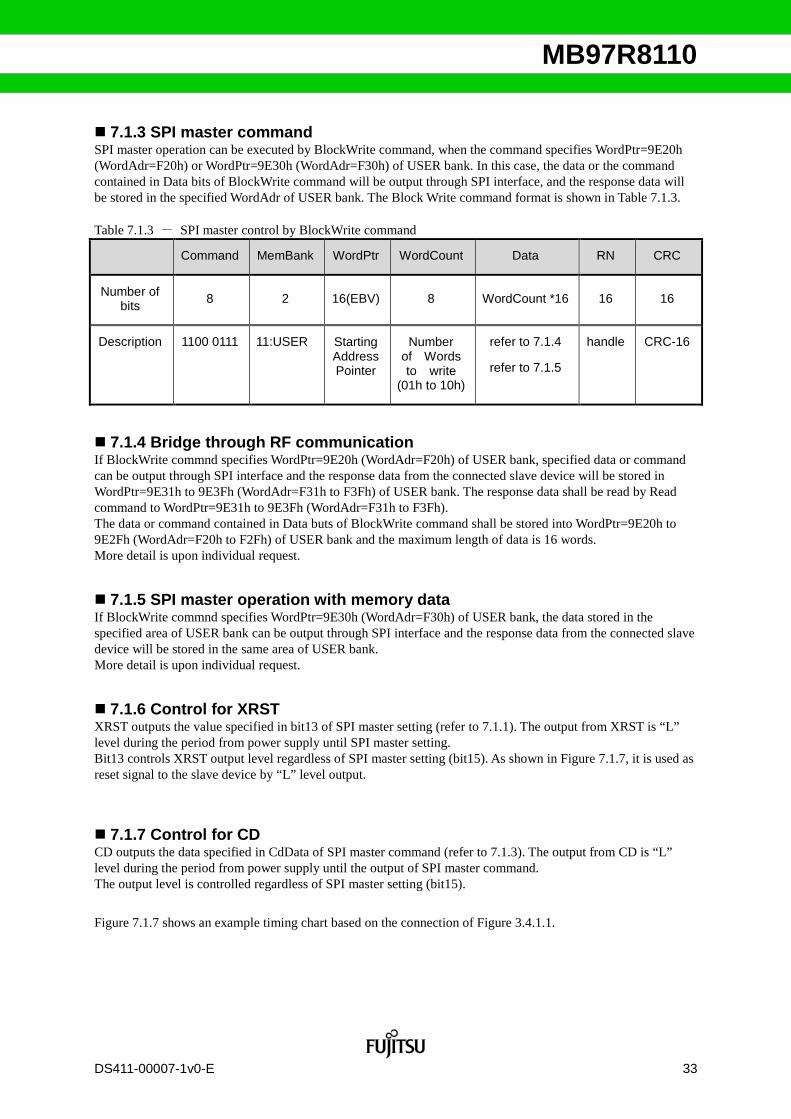
7.1 SPI master
7.1.1 SPI master setting SPI master mode is enabled by BlockWrite command to WordPtr=9E02h(WordAdr=F02h) of USER bank. It is necessary to enable setting every power on cycle. The setting value can be read by Read command, but the value will be reset to “0000h” under the following condition. • Power off after setting • Internal reset by low power detection In these cases, it is necessary to set the value again by BlockWrite command in order to enable SPI master mode. The data format of SPI master setting register is shown in Table7.1.1. Table 7.1.1 –Data format of SPI Master setting MSB LSB15 14 13 12 11 10 9 8 7 6 5 4 3 2 1 0
EnMuxDio
RstCtl
TestUse
SetupStart TestUse DivClk
En: Master operation Enable/Disable setting
bit Initial value Setting Setting description
15 0 0 SPI master operation Disable 1 SPI master operation Enable
MuxDio: Multiplex setting for DI and DO (refer to Chapter 7.1.2)
bit Initial value Setting Setting description
14 0 0 Separate for DI and DO 1 Multiplex for DI and DO
RstCtl: XRST control
bit Initial value Setting Setting description
13 0 0 XRST is "L" level output 1 XRST is "H" level output
TestUse
bit Initial value Setting Setting description
12 0 0 Set to 0 SetupStart[3:0]: setting number of clock cycles between command receiving and XCS dropping
bit Initial value Setting Setting description
11:8 0h N Setup=N*8 clock (N=1 to 15) Clock Frequency above is SCK output frequency described in DivClk. TestUse
bit Initial value Setting Setting description
7:4 - 0h Set to 0

DS411-00007-1v0-E 31
MB97R8110
DivClk[3:0] Clock division setting (SCK output frequency)
bit Initial value Setting SCK output frequency Setting description
3:0 0h M 0.5MHz/(M+1) DR=1(64/3) 0.5MHZ/(M+1) DR=0(8), TRcal<62.5us 0.5MHz/(M+1)/2 DR=0(8), 62.5us<TRcal<100us 0.5MHz/(M+1)/4 DR=0(8), 100us<TRcal<150us 0.5MHz/(M+1)/8 DR=0(8), 150us<TRcal<200us
SCK output frequency will be the result which 0.5MHz divided by the value plus 1 which is set by DivClk if the specified DR is 1(64/3)by Query command. SCK output frequency will depend on TRcal of Preamble and will be the value in the above Table if the specified DR is 0(8) by Query command.
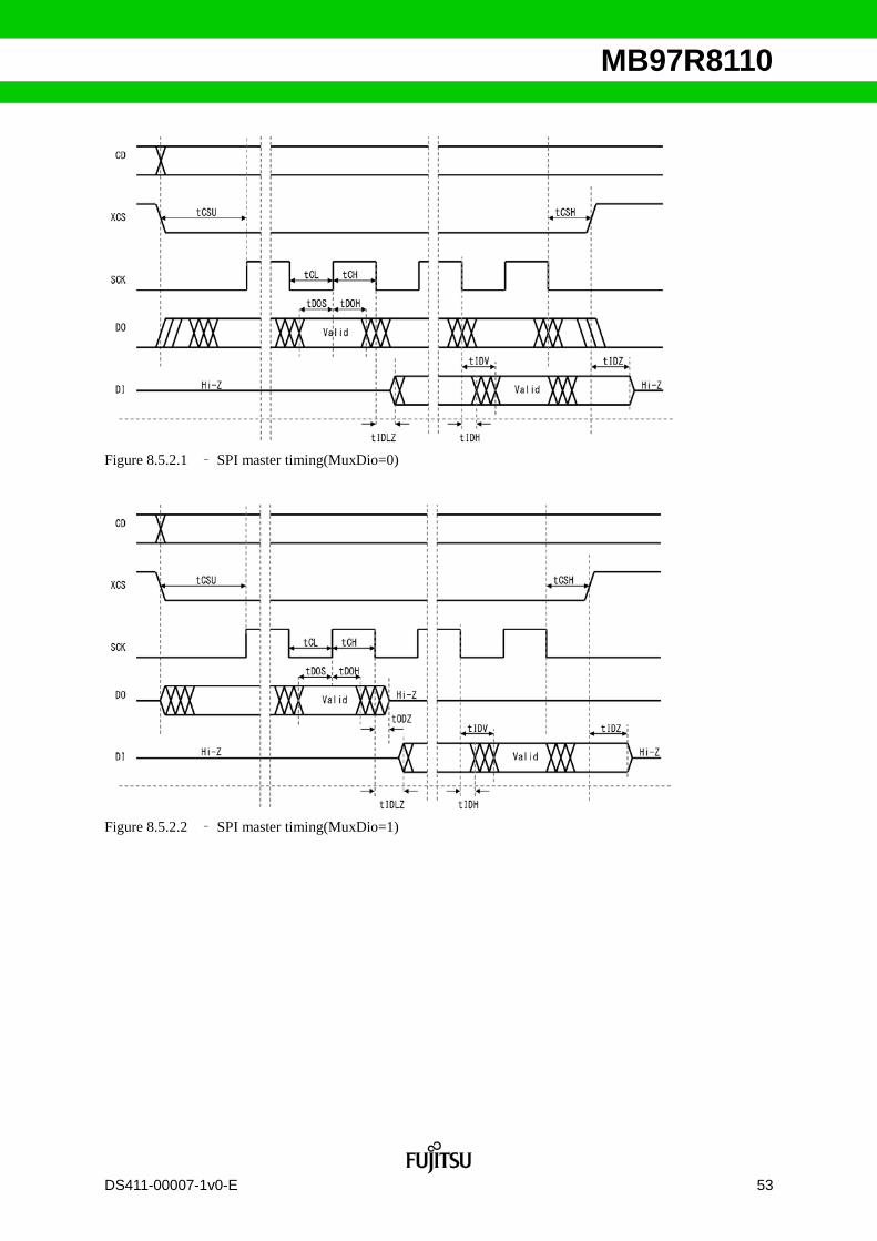
7.1.2 DI and DO Control (MuxDio)
7.1.2.1 Separate DI and DO Figure 7.1.2.1 shows the SPI master sequence with separate DI and DO, when bit14 of WordPtr=9E02h (WordAdr=F02h) of USER bank is set to “0”. During the SPI master operation, the output from DO is always “L” level or “H” level. The input to DI starts from the timing specified by DiPtr and receive data until XCS will be raised. The other period is invalid.
Figure 7.1.2.1 –Separate DI and DO (MuxDio=0)

32 DS411-00007-1v0-E
MB97R8110
7.1.2.2 Multiplex DI and DO Figure 7.1.2.2.1 and Figure 7.1.2.2.2 show the SPI master sequence with multiplex DI and DO, when bit14 of WordPtr=9E02h (WordAdr=F02h) of USER bank is set to “1”. In this condition, DI and DO is assumed to share common bus (DI/DO bus). During the period of the output from DO, the SPI slave device shall stay DI/DO bus “Hi-Z”. The input to DI starts from the timing specified by DiPtr and receive data until XCS will be raised. The other period is invalid.
Figure 7.1.2.2.1 - Multiplex DI and DO (MuxDio=1) (DiPtr<DoLength)
Figure 7.1.2.2.2 – Multiplex DI and DO /No data reception (MuxDio=1) (DiPtr>=DoLength)
DS411-00007-1v0-E 33
MB97R8110
7.1.3 SPI master command SPI master operation can be executed by BlockWrite command, when the command specifies WordPtr=9E20h (WordAdr=F20h) or WordPtr=9E30h (WordAdr=F30h) of USER bank. In this case, the data or the command contained in Data bits of BlockWrite command will be output through SPI interface, and the response data will be stored in the specified WordAdr of USER bank. The Block Write command format is shown in Table 7.1.3. Table 7.1.3 - SPI master control by BlockWrite command
Command MemBank WordPtr WordCount Data RN CRC
Number of bits 8 2 16(EBV) 8 WordCount *16 16 16
Description 1100 0111 11:USER
Starting Address Pointer
Number of Words to write
(01h to 10h)
refer to 7.1.4
refer to 7.1.5
handle CRC-16
7.1.4 Bridge through RF communication If BlockWrite commnd specifies WordPtr=9E20h (WordAdr=F20h) of USER bank, specified data or command can be output through SPI interface and the response data from the connected slave device will be stored in WordPtr=9E31h to 9E3Fh (WordAdr=F31h to F3Fh) of USER bank. The response data shall be read by Read command to WordPtr=9E31h to 9E3Fh (WordAdr=F31h to F3Fh). The data or command contained in Data buts of BlockWrite command shall be stored into WordPtr=9E20h to 9E2Fh (WordAdr=F20h to F2Fh) of USER bank and the maximum length of data is 16 words. More detail is upon individual request.
7.1.5 SPI master operation with memory data If BlockWrite commnd specifies WordPtr=9E30h (WordAdr=F30h) of USER bank, the data stored in the specified area of USER bank can be output through SPI interface and the response data from the connected slave device will be stored in the same area of USER bank. More detail is upon individual request.
7.1.6 Control for XRST XRST outputs the value specified in bit13 of SPI master setting (refer to 7.1.1). The output from XRST is “L” level during the period from power supply until SPI master setting. Bit13 controls XRST output level regardless of SPI master setting (bit15). As shown in Figure 7.1.7, it is used as reset signal to the slave device by “L” level output.
7.1.7 Control for CD CD outputs the data specified in CdData of SPI master command (refer to 7.1.3). The output from CD is “L” level during the period from power supply until the output of SPI master command. The output level is controlled regardless of SPI master setting (bit15). Figure 7.1.7 shows an example timing chart based on the connection of Figure 3.4.1.1.

34 DS411-00007-1v0-E
MB97R8110
Figure 7.1.7 control for XRST pin and CD pin
VDOUT3 is generated from RF and outputs to VDIO as IO power source. After SPI Master function is enabled by bit15 of SPI Master setting (refer to 7.1.1), XCS will be “H” level to output voltage to SPI slave device through COM0.

DS411-00007-1v0-E 35
MB97R8110
7.2 GPIO
7.2.1 GPIO Setting by Write operation GPIO function is enabled by BlockWrite command to WordPtr=9E00h (WordAdr=F00h) of USER bank in order to control the status of COM[2:0] and INT. The setting value can be read by Read command, but the value will be reset to “0000h” under the following condition. • Power off after setting • Internal reset by low power detection In these cases, it is necessary to set the value again by BlockWrite command in order to enable GPIO function. The data format of GPIO setting is shown in Table7.2.1. Table 7.2.1 GPIO control register format
MSB LSB
15 14 13 12 11 10 9 8 7 6 5 4 3 2 1 0
IntDat ComDat[2:0]FuncEn[3:0] TestUse SetEn[3:0]
FuncEn[3]:Data input setting of INT pin bit Initial
value Setting Setting Description
15 0 0 INT Input is rejected 1 INT input is accepted, and IntData will be updated by INT input
FuncEn[2:0]:Output setting of ComDat[2:0]
bit Initial value
Setting Setting Description
14 0 0 COM2 stays “Hi-Z” level 1 COM2 enables to output ComDat[2] setting
13 0 0 COM1 stays “Hi-Z” level 1 COM1 enables to output ComDat[1] setting
12 0 0 COM0 stays “Hi-Z” level 1 COM0 enables to output ComDat[0] setting
TestUse
bit Initial value
Setting Setting Description
11:8 0h 0h Set to 0 SetEn[3:0]:Update FuncEn[3:0] with [IntDat, ComDat[2:0]}
bit Initial value
Setting Setting Description
7 0 0 Nothing updated on FuncEn[3] 1 Update FuncEn[3] with IntDat
6 0 0 Nothing updated on FuncEn[2] 1 Update FuncEn[2] with ComDat[2]

36 DS411-00007-1v0-E
MB97R8110
5 0 0 Nothing updated on FuncEn[1] 1 Update FuncEn[1] with ComDat[1]
4 0 0 Nothing updated on FuncEn[0] 1 Update FuncEn[0] with ComDat[0]
IntDat:INT input data
bit Initial value
Setting Setting Description
3 0 0 IntDat Not updated by INT input 1 IntDat Updated by INT input
ComDat[2:0]:COM output data
bit Initial value
Setting Setting Description
2 0 0 “0” output from COM2 1 “1” output from COM2
1 0 0 “0” output from COM1 1 “1” output from COM1
0 0 0 “0” output from COM0 1 “1” output from COM0
7.2.2 Reading GPIO setting The GPIO status information (Table 7.2.1) can be read by Read command to WordPtr=9E00h (WordAdr=F00h). FuncEn[3]:IndtDat setting
bit Initial value
Setting Read Value
15 0 0 (Setting information) INT Input is rejected 1 (Setting information) INT input is accepted, and InDat is updated
FuncEn[2:0]:Com[2:0] setting
bit Initial value
Setting Read Value
14 0 0 (Setting information) ComDat[2]=”0”output 1 (Setting information) ComDat[2]=“1”output
13 0 0 (Setting information) ComDat[1]=”0”output 1 (Setting information) ComDat[1]= “1”output
12 0 0 (Setting information) ComDat[0]= ”0”output 1 (Setting information) ComDat[0]= “1”output

DS411-00007-1v0-E 37
MB97R8110
SetEn[3:0]:Write control bit Initial
value Setting Read Value
7:4 0h - “0h” (Write only)
7.2.3 GPIO Setting Example
7.2.3.1 INT control Truth table of INT control is shown in Table 7.2.3.1. Table 7.2.3.1 INT Truth Table
7.2.3.2 COM[2:0] control Truth table of COM[2:0] control is shown in Table 7.2.3.2. Table 7.2.3.2 COM[2:0] Truth Table
FuncEn IntDat SetEn FuncEn IntDat INT IO FuncEn IntDat0 0 0 1 1 - 0 0 Rejected0 1 0 1 0 - 0 1 Rejected1 0 0 0 1 0 1 0 Accepted1 1 0 0 0 1 1 1 Accepted0 0 1 1 1 0 1 0 Accepted0 1 1 1 0 1 1 1 Accepted1 0 1 0 1 - 0 1 Rejected1 1 1 0 0 - 0 0 Rejected
StatusBefore Setting Setting Data Status
After Setting INTINPUT
FuncEn ComDat SetEn FuncEn ComDat FuncEn ComDat0 0 0 1 1 0 0 Hi-Z0 0 0 1 0 0 0 Hi-Z1 0 0 0 1 1 0 01 1 0 0 0 1 1 10 0 1 1 1 1 1 10 0 1 1 0 1 0 01 0 1 0 1 0 0 Hi-Z1 1 1 0 0 0 0 Hi-Z
StatusBefore Setting Setting Data Status
After Setting COMOut

38 DS411-00007-1v0-E
MB97R8110
7.3 Key Matrix scan
7.3.1 Key Matrix scan setting Key Matrix scan function is enabled by BlockWrite command to WordPtr=9E01h(WordAdr=F01h) of USER bank. It is necessary to enable setting every power on cycle. The setting value can be read by Read command, but the value will be reset to “0000h” under the following condition. • Key Matrix scan Disable(bit15="0") • Power off after setting • Internal reset by low power detection In these cases, it is necessary to set the value again by BlockWrite command in order to enable Key Matrix scan function. The data format of Key Matrix scan setting register is shown in Table7.3.1. Table 7.3.1 –Data format of Key Matrix scan setting MSB LSB
15 14 13 12 11 10 9 8 7 6 5 4 3 2 1 0
En LastColumn TestUseTime
SampleTestUse
En: Key Matrix scan operation Enable/Disable
bit Initial value Setting value Setting description
15 0h 0 Key Matrix scan operation Disable 1 Key Matrix scan operation Enable
TimeSample:Activate time for Column 1(Reference value for enough power supply)
bit Initial value Setting value Setting description
14:13 0h 0h 256us 1h 512us 2h 64us 3h 128us
Test Use
bit Initial value Setting value Setting description
12:8 0h 0h Set to 0 LastColumn
bit Initial value Setting value Setting description
7:4 0h 3h* to Fh Specify “the connected Number of Column -1” *. When the number of column is less than 4, set to “3h”. Test Use
bit Initial value Setting value Setting description
3:0 0h 0h Set to 0

DS411-00007-1v0-E 39
MB97R8110
7.3.2 Block Erase Command for Key Matrix scan Key Matrix scan function is executed by BlockErase command to WordPtr=9E10h (WordAdr=F10h) of USER bank, and detects the key input status of the connected device as shown in Figure 3.6.1. Up to 4 columns of key information, which include pressed key, are stored in WordPtr=9E10h to 9E13h (WordAdr=F10h to F13h). The Command format is shown in Table.7.3.2. Table 7.3.2 - Key Matrix scan with BlockErase command
Command MemBank WordPtr WordCount RN CRC
Number of bits 8 2 16(EBV) 8 16 16
Description 1100 1000 11:USER
1001 1110 0001 0000
LastColumn+1
(refer to 7.3.1)
handle CRC-16
7.3.3 Response to Block Erase Command The error code “8Eh” will be replied if there are no pressed Keys when Key Matrix scan command is executed by BlockErase. The normal reply will be returned if the pressed keys of 1Column to 4Column are detected. The error code “0Bh” (indicating Insufficient power) will be replied if internal voltage during Key Matrix scan operation caused is dropped down.
7.3.4 Read Command for reading Key data The pressed Key data will be confirmed by Read command to WordPtr= 9E10h to 9E13h (WordAdr=F10h to F13h). The Command format is shown in Table.7.3.4. Table 7.3.4 - Key data confirmation with Read command
Command MemBank WordPtr WordCount RN CRC
Number of bits 8 2 16 (EBV) 8 16 16
Description 1100 0010 11:USER
1001 1110 0001 0000
04h Count of key data to read
handle CRC-16

40 DS411-00007-1v0-E
MB97R8110
7.3.5 Key data format The pressed key data is stored to WordPtr=9E10h to 9E13h (WordAdr=F10h to F13h) in the format as shown in Table 7.3.5 Table 7.3.5 Key Matrix scan data format
MSB LSB15 14 13 12 11 10 9 8 7 6 5 4 3 2 1 0
0h KC KR
KC: Column number (KC00 to KC15) of Key Matrix bit Initial
value
Retrieved
value
Description
11:8 0h N KC Pin Number (N= 0 to Fh)
e.g. 0111b for KC7
KR:Raw data (KR00 to KR07) of Key Matrix bit Initial
value
Retrieved
value
Description
7:0 0h xxxx
xxxxb
8bits of Key information on the detected KC[11:8]
e.g. 00110000b for the input to KR04 and KR05
(refer to Figure 7.3.8)
One command cycle updates WordPtr=9E10h to 9E13h (WordAdr=F10h to F13h), where 4 columns of data is stored. If the detected number of columns is less than 4, the same number of word will be updated and the rest will be cleared to 0000h. For example, if the detected column is only 1, the data stored in WordPtr=9E11h to 9E13h (WordAdr=F11h to F13h) will be cleared to 0000h.
7.3.6 Key Matrix scan interface input/output Once Key Matrix scan starts, “H” level of activation signal switches to select to the columns from KC00 to KC15. When the column is not selected, the output is “Hi-Z”. When the pressed key is detected, the data outputs. Figure 7.3.6 describes an example that KR05 is pressed on KC01 Column, and it takes 4ms to scan 16 Columns.
Figure 7.3.6 -Key Matrix scan signal input/output

DS411-00007-1v0-E 41
MB97R8110
7.3.7 Communication flow The communication flow among reader/writer, this LSI and Key input device is described in Figure 7.3.7 The scan operation for Key input device will be processed during T5 time (Max 20ms) of EPC starting from receipt of BlockErase command to reply
Figure 7.3.7 - Key Matrix scan operation communication flow

42 DS411-00007-1v0-E
MB97R8110
7.3.8 The pressed Key number and Key Matrix scan clock operation The number of scanned data is up to 4 columns once one BlockErase command is executed. Figure 7.3.8 describes an example of 8x16 Key Matrix scan that there are 5colums with pressed Keys. In the example, the scan column will stop at KC10 where the 4th Key data is scanned, and the data 0080h, 0102h, 0430h, 0A01h will be stored respectively into WordPtr=9E10h to 9E13h (WordAdr=F10h to F13h) of USER bank as the 1st output of scan. It is identified that KR05 and KR04 Keys are pressed simultaneously on KC04. This LSI will reply to BlockErase normally after 4 column data is stored in the memory. Upon the next BlockErase command, the scan will start from KC11 which is the next column to KC10 the last scan of the 1st output. If the Key Matrix scan operation reaches to KC15, it backs to KC00 as 2nd round and continues scanning until detecting all 4 column data or accumulated scanning column reaches 16, and then data will be stored as the 2nd output. The example shows that the data 0F40h, 0080h, 0102h, 0430h will be stored respectively into WordPtr=9E10h to 9E13h (WordAdr=F10h to F13h) of USER bank.
Figure 7.3.8 - Key Matrix scan operation communication flow
1st Round 1st Round(cont.) 2nd Round0 0 0 0 0 0 0 0 0 0 0 0 0 0 0 0 0 0 0 0 0 0 0 0 0 0 0 0 0 0 0 0 0 0 0 0 0 0 0 0 0 0 0 0 0 0 0 0
0 0 0 0 0 0 0 0 0 0 0 0 0 0 0 0 0 0 0 0 0 0 0 0 0 0 0 0 0 0 0 0 0 0 0 0 0 0 0 0 0 0 0 0 0 0 0 0
0 0 0 0 0 0 0 0 0 0 0 0 0 0 0 0 0 0 0 0 0 0 0 0 0 0 0 0 0 0 0 0 0 0 0 0 0 0 0 0 0 0 0 0 0 0 0 0
0 0 0 0 0 0 0 0 0 0 0 0 0 0 0 0 0 0 0 0 0 0 0 0 0 0 0 0 0 0 0 0 0 0 0 0 0 0 0 0 0 0 0 0 0 0 0 0
KC00
KC01
KC02
KC03
KC04
KC05
KC06
KC07
KC08
KC09
KC10
KC11
KC12
KC13
KC14
KC15
KC00
KC01
KC02
KC03
KC04
KC05
KC06
KC07
KC08
KC09
KC10
KC11
KC12
KC13
KC14
KC15
KC00
KC01
KC02
KC03
KC04
KC05
KC06
KC07
KC08
KC09
KC10
KC11
KC12
KC13
KC14
KC15
0 0 0 0 0 0 0 0 1 1 1 1 1 1 1 1 0 0 0 0 0 0 0 0 1 1 1 1 1 1 1 1 0 0 0 0 0 0 0 0 1 1 1 1 1 1 1 1
0 0 0 0 1 1 1 1 0 0 0 0 1 1 1 1 0 0 0 0 1 1 1 1 0 0 0 0 1 1 1 1 0 0 0 0 1 1 1 1 0 0 0 0 1 1 1 1
0 0 1 1 0 0 1 1 0 0 1 1 0 0 1 1 0 0 1 1 0 0 1 1 0 0 1 1 0 0 1 1 0 0 1 1 0 0 1 1 0 0 1 1 0 0 1 1
0 1 0 1 0 1 0 1 0 1 0 1 0 1 0 1 0 1 0 1 0 1 0 1 0 1 0 1 0 1 0 1 0 1 0 1 0 1 0 1 0 1 0 1 0 1 0 1
KR07 1 0 0 0 0 0 0 0 0 0 0 0 0 0 0 0 KR07 1 0 0 0 0 0 0 0 0 0 0 0 0 0 0 0 1 0 0 0 0 0 0 0 0 0 0 0 0 0 0 0
KR06 0 0 0 0 0 0 0 0 0 0 0 0 0 0 0 1 KR06 0 0 0 0 0 0 0 0 0 0 0 0 0 0 0 1 0 0 0 0 0 0 0 0 0 0 0 0 0 0 0 1
KR05 0 0 0 0 1 0 0 0 0 0 0 0 0 0 0 0 KR05 0 0 0 0 1 0 0 0 0 0 0 0 0 0 0 0 0 0 0 0 1 0 0 0 0 0 0 0 0 0 0 0
KR04 0 0 0 0 1 0 0 0 0 0 0 0 0 0 0 0 KR04 0 0 0 0 1 0 0 0 0 0 0 0 0 0 0 0 0 0 0 0 1 0 0 0 0 0 0 0 0 0 0 0
KR03 0 0 0 0 0 0 0 0 0 0 0 0 0 0 0 0 KR03 0 0 0 0 0 0 0 0 0 0 0 0 0 0 0 0 0 0 0 0 0 0 0 0 0 0 0 0 0 0 0 0
KR02 0 0 0 0 0 0 0 0 0 0 0 0 0 0 0 0 KR02 0 0 0 0 0 0 0 0 0 0 0 0 0 0 0 0 0 0 0 0 0 0 0 0 0 0 0 0 0 0 0 0
KR01 0 1 0 0 0 0 0 0 0 0 0 0 0 0 0 0 KR01 0 1 0 0 0 0 0 0 0 0 0 0 0 0 0 0 0 1 0 0 0 0 0 0 0 0 0 0 0 0 0 0
KR00 0 0 0 0 0 0 0 0 0 0 1 0 0 0 0 0 KR00 0 0 0 0 0 0 0 0 0 0 1 0 0 0 0 0 0 0 0 0 0 0 0 0 0 0 1 0 0 0 0 0
Data
00800102
043 0
0A01
0F4000800102
043 0
WordPtr
9E10h9E11h
9E12h
9E13h
9E10h9E11h9E12h
9E13h
Stop
Stop
BlockErase KeyScan Response BlockErase KeyScan ResponseTime

DS411-00007-1v0-E 43
MB97R8110
7.4 VDOUT3 Power output
7.4.1 VDOUT3 setting VDOUT3 is power output function, which generates RF power through PWRP3-PWPM3 and provide it for external devices. This function is enabled by BlockWrite command to WordPtr=9E03h(WordAdr=F03h) of USER bank in order to set the conditions of voltage detection. It is necessary to enable setting every power on cycle. The detected voltage status is stored in bit1 to 2 and can be confirmed by Read command. The data format of VDOUT3 setting is shown in Table7.4.1. Table 7.4.1 –Data format of VDOUT3 setting MSB LSB
15 14 13 12 11 10 9 8 7 6 5 4 3 2 1 0
En
Det1
En
Det2SetVolDet1 SetVolDet2 TestUse VolDet
EnDet1 “SetVolDet1” Enable/Disable setting
bit Initial value Setting value Setting description
15 0 0 Voltage detection Disabled (SetVoDet1 is invalid) 1 Voltage detection Enabled (SetVoDet1 is valid)
SetVolDet1 Lower limit setting of Output voltage(VolDet1)
bit Initial value Setting value Setting description
14:12 0 0h 3.1±0.25V 1h 3.0±0.25V 2h 2.9±0.25V 3h 2.8±0.25V 4h 2.7±0.25V 5h 2.6±0.25V 6h 2.5±0.25V 7h 2.4±0.25V
EnDet2 “SetVolDet2” Enable/Disable setting
bit Initial value Setting value Setting description
11 0 0 Voltage detection Disabled (SetVoDet2 is invalid) Only the detection voltages setting is disabled, and Output Voltage (MAX) is not Disabled. (See SetHigVol)
1 Voltage detection Enabled (SetVoDet2 is valid)

44 DS411-00007-1v0-E
MB97R8110
SetVolDet2 Upper limit setting of Output voltage(VolDet2) bit Initial value Setting value Setting description Output Voltage (Max)※
10:8 0 0h 3.3±0.25V 3.6V 1h 3.2±0.25V 3.6V 2h 3.1±0.25V 3.5V 3h 3.0±0.25V 3.5V 4h 3.0±0.25V 3.4V 5h 2.9±0.25V 3.4V 6h 2.8±0.25V 3.3V 7h 2.7±0.25V 3.3V
※ Regardless of bit11 setting of EnDet2, Maximum output voltage level is always effective by this setting. Test Use
bit Initial value Setting value Setting description
7:2 0 0h Set to 0 VolDet (Read only)
bit Initial value Setting value Setting description
1 - 0h VDOUT3<SetVolDet1 1h VDOUT3>SetVolDet1
0 - 0h VDOUT3<SetVolDet2 1h VDOUT3>SetVolDet2
7.4.2 VDOUT3 Output current on receiving power Figure 7.4.2 shows the VDOUT3 output current with 3V power supply on different receiving power level
from RF (PWRP3-PWRM3 antenna). In this figure, 600μA with 3V output requires +8dBm as receiving power from RF.
Figure 7.4.2 VDOUT3 output current with 3V power supply
DS411-00007-1v0-E 45
MB97R8110
8 ELECTRICAL CHARACTERISTICS
8.1 Absolute Maximum Rating Table 8.1 - Absolute Maximum Rating
Parameter Symbol Value
Unit Conditions/Remarks MIN TYP MAX
Maximum input voltage Vmax - - 4.0 V PWRP1-PWRM1,PWRP3-PWRM3
Power supply voltage VDD -0.5 - +4.0 V
Input voltage VIN -0.5 - VDD+0.5 V
Output voltage VOUT -0.5 - VDD+0.5 V
ESD voltage immunity VESD - - ±1200 V Human Body Model
Storage temperature Tstg -40 - +85 ℃
8.2 Recommended Operation Conditions Table 8.2 - Recommended Operation Conditions
Parameter Symbol Value
Unit Conditions/Remarks MIN TYP MAX
Operating
ambient temperature
Ta -40 - +85 ℃
Retention
guaranteed temperature
Trtn1 -40 - +85 ℃ Retention guaranteed period: 10years
RF communication
Antenna input frequency
Fclk 860 - 960 MHz
Reception
modulation depth
(A-B)/A 80 90 100 %
Receiving bit rate F_fwd 26.7 - 128 kbps PIE code: mark rate =1/2
Receiving
waveform rise time
Tr 1 - 500 µs
Receiving
waveform settling time
Ts - - 1500 µs
Receiving
waveform fall time
Tf 1 - 500 µs

46 DS411-00007-1v0-E
MB97R8110
SPI slave communication Power supply voltage VDD 1.8 - 3.6 V
“H” level input voltage VIH VDD-
0.2 - VDD +0.3 V
“L” level input voltage VIL -0.3 - +0.4 V
8.3 RF Communication Characteristics Table 8.3 – RF Communication Characteristics
Parameter Symbol Value
Unit Conditions/Remarks MIN TYP MAX
Minimum operating power when reading
PR_MIN - -12 - dBm Measured with bare die Tari=25us,RTcal=2.5Tari,TRcal=3.0RTcal, DR=8,FM0,BLF=43kbps, DSB-ASK, Modulation depth==90% memory access length≦6Word (※1)
Minimum operating power when writing
PW_MIN - -12 - dBm
Maximum operating power PMAX +20 dBm
Equivalent input capacitance
(PWRP1-PWRM1) CP
- 0.8 - pF 920MHz: Input power= -12dBm, parallel model
- 0.8 - pF 866MHz: Input power= -12dBm, parallel model
Equivalent input resistance
(PWRP1-PWRM1) RP
- 4.1 - KΩ 920MHz: Input power= -12dBm, parallel model
- 4.9 - KΩ 866MHz: Input power= -12dBm, parallel model
Equivalent input capacitance
(PWRP3-PWRM3) CP
- 2.5 - pF 920MHz: Input power= +8dBm, parallel model
- 2.3 - pF 866MHz: Input power= +8dBm, parallel model
Equivalent input resistance
(PWRP1-PWRM1) RP
- 140 - Ω 920MHz: Input power= +8dBm, parallel model
- 155 - Ω 866MHz: Input power= +8dBm, parallel model
Returning bit rate F_rtrn 40 640 kbps
※1 These characteristics are the values for the standalone LSI, and do not specify the values when the LSI is connected to other devices.

DS411-00007-1v0-E 47
MB97R8110
8.4 SPI Slave Communication
8.4.1 DC Characteristics Table 8.4.1 – DC Characteristics
Parameter Symbol Value
Unit Conditions MIN TYP MAX
Input leakage current
ILI ― ― ±5 μA VIN = VDD (SPIREQ pin)
― ― ±1 µA VIN = 0V (SPIREQ pin)
VIN = 0V to VDD (the other pins※1)
Output leakage current
ILO ― ― ±1 μA VOUT = 0V to VDD, when output is “Hi-Z” (output pin ※2)
Power supply
ICC ICC ― 70 200 μA SCK = 2MHz, Vdd=3.0V
IPD1 IPD1 ― 1 10 μA SPIREQ = 0V or open No RF reception
ISB ISB ― 20 40 μA SPIREQ = VDD XCS=VDD
“H” level Input voltage
VIH VDDx0.7 ― VDD+0.5 V ※3
“L” level Input voltage
VIL -0.5 ― VDDx0.3 V ※3
“H” level Output voltage
VOH VDD-0.5 ― VDD V IOH=-2mA ※2
“L” level Output voltage
VOL 0 ― 0.4 V IOL= 2mA ※2
SPI pin pull-down resistance
RIN 0.8 1 1.2 MΩ VIN = VDD SPIREQ Pin
※1:XCS、SCK、DI Pin ※2:DO、SPIACK Pin ※3:SPIREQ、XCS、SCK、DI Pin
48 DS411-00007-1v0-E
MB97R8110
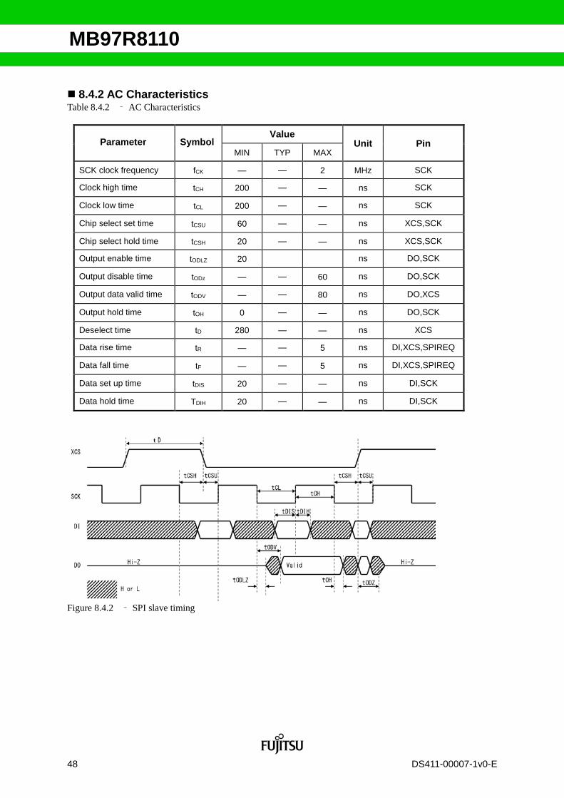
8.4.2 AC Characteristics Table 8.4.2 – AC Characteristics
Parameter Symbol Value
Unit Pin MIN TYP MAX
SCK clock frequency fCK ― ― 2 MHz SCK
Clock high time tCH 200 ― ― ns SCK
Clock low time tCL 200 ― ― ns SCK
Chip select set time tCSU 60 ― ― ns XCS,SCK
Chip select hold time tCSH 20 ― ― ns XCS,SCK
Output enable time tODLZ 20 ns DO,SCK
Output disable time tODz ― ― 60 ns DO,SCK
Output data valid time tODV ― ― 80 ns DO,XCS
Output hold time tOH 0 ― ― ns DO,SCK
Deselect time tD 280 ― ― ns XCS
Data rise time tR ― ― 5 ns DI,XCS,SPIREQ
Data fall time tF ― ― 5 ns DI,XCS,SPIREQ
Data set up time tDIS 20 ― ― ns DI,SCK
Data hold time TDIH 20 ― ― ns DI,SCK
Figure 8.4.2 – SPI slave timing
DS411-00007-1v0-E 49
MB97R8110
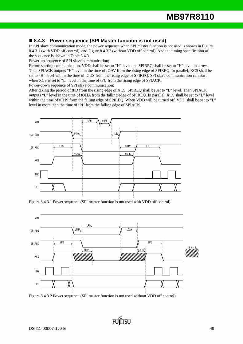
8.4.3 Power sequence (SPI Master function is not used) In SPI slave communication mode, the power sequence when SPI master function is not used is shown in Figure 8.4.3.1 (with VDD off control), and Figure 8.4.3.2 (without VDD off control). And the timing specification of the sequence is shown in Table.8.4.3. Power-up sequence of SPI slave communication; Before starting communication, VDD shall be set to “H” level and SPIREQ shall be set to “H” level in a row. Then SPIACK outputs “H” level in the time of tOAV from the rising edge of SPIREQ. In parallel, XCS shall be set to “H” level within the time of tCUS from the rising edge of SPIREQ. SPI slave communication can start when XCS is set to “L” level in the time of tPU from the rising edge of SPIACK. Power-down sequence of SPI slave communication; After taking the period of tPD from the rising edge of XCS, SPIREQ shall be set to “L” level. Then SPIACK outputs “L” level in the time of tOHA from the falling edge of SPIREQ. In parallel, XCS shall be set to “L” level within the time of tCHS from the falling edge of SPIREQ. When VDD will be turned off, VDD shall be set to “L” level in more than the time of tPH from the falling edge of SPIACK.
Figure 8.4.3.1 Power sequence (SPI master function is not used with VDD off control)
Figure 8.4.3.2 Power sequence (SPI master function is not used without VDD off control)

50 DS411-00007-1v0-E
MB97R8110
Table 8.4.3 Timing specifications during SPI slave communication
Parameter Symbol Value
Unit MIN TYP MAX
SPIREQ rising start time tSU 500 ― ― µs
SPIREQ low time tRQL 1000 ― ― µs
Power hold time tPH 0 ― ― µs
XCS level hold time at power ON tPU 10 ― ― µs
XCS level hold time at power OFF tPD 1 ― ― µs
Power off time tOFF 1000 ― ― µs
Output SPIACK definite time tOAV 1 ― 20000 µs
Output SPIACK hold time tOHA 5 ― 10000 ns
XCS setup time(start) tCUS ― ― 1 µs
XCS hold time(start) tCHS 0 ― µs
If the device does not operate within the specified conditions of cycle or power on/off sequence, memory data cannot be guaranteed.

DS411-00007-1v0-E 51
MB97R8110
8.4.4 Power Sequence (SPI Master function is used) In SPI slave communication mode, the power sequence when SPI master function is used is shown in Figure 8.4.4.1 (with VDD off control), and Figure 8.4.4.2 (without VDD off control). And the timing specification of the sequence is in common as shown in Table.8.4.3. Power-up sequence of SPI slave communication; Before starting communication, VDD shall be set to “H” level and SPIREQ shall be set to “H” level in a row. Then SPIACK outputs “H” level in the time of tOAV from the rising edge of SPIREQ. At this point, XCS and SCK shall be “Hi-Z” because SPI master operation may have been used during the period when SPI has been “L” level. XCS shall be set to “H” level within the period of tCUS from the rising edge of SPIACK, and SCK shall be set to “L” level at the same time. SPI slave communication can start when XCS is set to “L” level in the time of tPU from the rising edge of SPIACK. Power-down sequence of SPI slave communication; After taking the period of tPD from the rising edge of XCS, SPIREQ shall be set to “L” level. Then SPIACK outputs “L” level in the time of tOHA from the falling edge of SPIREQ. After taking the time of tCHS from the falling edge of SPIACK, the input to XCS and SCK will be invalid and shall be set to “Hi-Z” in order to enable XCS and SCK for SPI master communication. When VDD will bew turned off, VDD shall be set to “L” level in the period of tPH from the falling edge of SPIACK.
Figure 8.4.4.1 Power sequence (SPI master function is used with VDD off control)
Figure 8.4.4.2 Power sequence (SPI master function is used without VDD off control)

52 DS411-00007-1v0-E
MB97R8110
8.5 SPI Master Communication
8.5.1 DC Characteristics Table 8.5.1 – DC Characteristics
Parameter Symbol Value
Unit Conditions MIN TYP MAX
Input leakage current ILI ― ― ±1 µA ※1
Output leakage current ILO ― ― ±1 µA "Hi-Z” state ※3
Power output voltage VDOUT3 2.95 ― 3.6 V refer to 7.4.2 ※2
“H” level Input voltage VIH VDOUT3×0.7 ― VDOUT3+0.5 V ※1
“L” level Input voltage VIL -0.5 ― VDOUT3×0.3 V ※1
“H” level Output voltage VOH VDOUT3-0.5 ― VDOUT3 V IOH=-0.5mA ※3
“L” level Output voltage VOL 0 ― 0.4 V IOL= 0.5mA ※3 ※1:DI Pin ※2:VDOUT3, VDIO Pin ※3:XCS, SCK, DO, CD, XRST Pin
8.5.2 AC Characteristics Table 8.5.2 –AC Characteristics
Parameter Symbol Value
Unit Related Pin MIN TYP MAX
SCK clock frequency fCK 3.67 ― 500 kHz SCK
Clock high time tCH 300 ― ― ns SCK
Clock low time tCL 300 ― ― ns SCK
Chip select setup time tCSU 600 ― ― ns XCS,CD,SCK
Chip select hold time tCSH 300 ― ― ns XCS,CD,SCK
Input enable time tIDLZ 10 ― ― ns DI
Input disable time tIDZ ― ― 1200 ns DI,XCS
Output setup time tDOS 35 ― ― ns DO,SCK
Output hold time tDOH 0 ― ― ns DO,SCK
Output disable time tODZ 0 ― 10 ns DO
Data rise time tR ― ― 5 ns DI
Data fall time tF ― ― 5 ns DI
Data confirm time tIDV ― ― 100 ns DI,SCK
Data hold time tIDH 10 ― ― ns DI,SCK
DS411-00007-1v0-E 53
MB97R8110
Figure 8.5.2.1 – SPI master timing(MuxDio=0)
Figure 8.5.2.2 – SPI master timing(MuxDio=1)
54 DS411-00007-1v0-E
MB97R8110
8.6 Key Matrix scan Characteristics
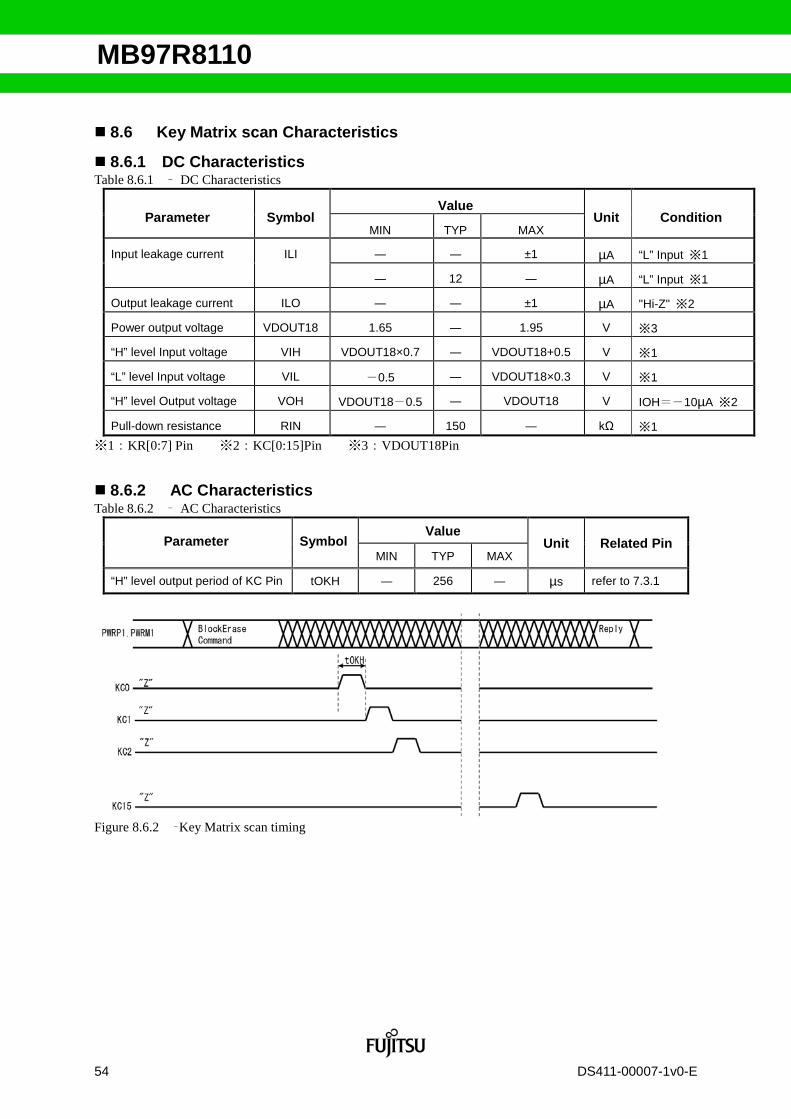
8.6.1 DC Characteristics Table 8.6.1 – DC Characteristics
Parameter Symbol Value
Unit Condition MIN TYP MAX
Input leakage current ILI ― ― ±1 µA “L” Input ※1
― 12 ― µA “L” Input ※1
Output leakage current ILO ― ― ±1 µA "Hi-Z" ※2
Power output voltage VDOUT18 1.65 ― 1.95 V ※3
“H” level Input voltage VIH VDOUT18×0.7 ― VDOUT18+0.5 V ※1
“L” level Input voltage VIL -0.5 ― VDOUT18×0.3 V ※1
“H” level Output voltage VOH VDOUT18-0.5 ― VDOUT18 V IOH=-10µA ※2
Pull-down resistance RIN ― 150 ― kΩ ※1 ※1:KR[0:7] Pin ※2:KC[0:15]Pin ※3:VDOUT18Pin
8.6.2 AC Characteristics Table 8.6.2 – AC Characteristics
Parameter Symbol Value
Unit Related Pin MIN TYP MAX
“H” level output period of KC Pin tOKH ― 256 ― µs refer to 7.3.1
Figure 8.6.2 –Key Matrix scan timing

DS411-00007-1v0-E 55
MB97R8110
8.7 GPIO Characteristics
8.7.1 DC Characteristics Table 8.7.1 – DC Characteristics
Parameter Symbol Value
Unit Conditions MIN TYP MAX
Input leakage current ILI ― ― ±1 µA ※1
Output leakage current ILO ― ― ±1 µA "Hi-Z" output ※2
“H” level Input voltage VIH VDIO×0.7 ― VDIO+0.5 V ※1, ※3
“L” level Input voltage VIL -0.5 ― VDIO×0.3 V ※1, ※3
“H” level Output voltage VOH VDIO-0.5 ― VDIO V IOH =-0.5mA ※2, ※3
“L” level Output voltage VOL 0 ― 0.4 V IOL = 0.5mA ※2 ※1:INT Pin ※2:COM[2:0] Pin ※3:VDIO voltage is selected either applied voltage from VDD or output voltage from VDOUT3
8.7.2 AC Characteristics Table 8.7.2 – AC Characteristics
Parameter Symbol Value
Unit Related Pin MIN TYP MAX
COM output update time tOCV ― ― 1 ms COM[2:0]
INT input setup time tIIS 0 ― ― INT ※1
INT input hold time tIIH ― ― T1 ms INT ※1
※1:INT information is read out at the input timing described in Table 8.7.2 and Figure 8.7.2.2. T1 is the T1 time specified in EPC standard.
Figure 8.7.2.1 – GPIO timing(COM output)
Figure 8.7.2.2 – GPIO timing(INT input)

56 DS411-00007-1v0-E
MB97R8110
9 Ordering Information Part Number Shipping Method Wafer thickness
MB97R8110-WF Wafer 725μm±20μm
10 Others
10.1 Note items Specifications are subject to change without notice. For further information please contact each office. All Rights Reserved. The contents of this document are subject to change without notice. Customers are advised to consult with sales representatives before ordering. The information, such as descriptions of function and application circuit examples, in this document are presented solely for the purpose of reference to show examples of operations and uses of FUJITSU SEMICONDUCTOR device; FUJITSU SEMICONDUCTOR does not warrant proper operation of the device with respect to use based on such information. When you develop equipment incorporating the device based on such information, you must assume any responsibility arising out of such use of the information. FUJITSU SEMICONDUCTOR assumes no liability for any damages whatsoever arising out of the use of the information. Any information in this document, including descriptions of function and schematic diagrams, shall not be construed as license of the use or exercise of any intellectual property right, such as patent right or copyright, or any other right of FUJITSU SEMICONDUCTOR or any third party or does FUJITSU SEMICONDUCTOR warrant non-infringement of any third-party's intellectual property right or other right by using such information. FUJITSU SEMICONDUCTOR assumes no liability for any infringement of the intellectual property rights or other rights of third parties which would result from the use of information contained herein. The products described in this document are designed, developed and manufactured as contemplated for general use, including without limitation, ordinary industrial use, general office use, personal use, and household use, but are not designed, developed and manufactured as contemplated (1) for use accompanying fatal risks or dangers that, unless extremely high safety is secured, could have a serious effect to the public, and could lead directly to death, personal injury, severe physical damage or other loss (i.e., nuclear reaction control in nuclear facility, aircraft flight control, air traffic control, mass transport control, medical life support system, missile launch control in weapon system), or (2) for use requiring extremely high reliability (i.e., submersible repeater and artificial satellite). Please note that FUJITSU SEMICONDUCTOR will not be liable against you and/or any third party for any claims or damages arising in connection with above-mentioned uses of the products. Any semiconductor devices have an inherent chance of failure. You must protect against injury, damage or loss from such failures by incorporating safety design measures into your facility and equipment such as redundancy, fire protection, and prevention of overcurrent levels and other abnormal operating conditions. Exportation/release of any products described in this document may require necessary procedures in accordance with the regulations of the Foreign Exchange and Foreign Trade Control Law of Japan and/or US export control laws. The company names and brand names herein are the trademarks or registered trademarks of their respective owners.
FUJITSU SEMICONDUCTOR LIMITED Shin-Yokohama Chuo Building, 2-100-45 Shin-Yokohama, Kohoku-ku, Yokohama, Kanagawa 222-0033, Japan http://jp.fujitsu.com/fsl/en/
All Rights Reserved. FUJITSU SEMICONDUCTOR LIMITED, its subsidiaries and affiliates (collectively, "FUJITSU SEMICONDUCTOR") reserves the right to make changes to the information contained in this document without notice. Please contact your FUJITSU SEMICONDUCTOR sales representatives before order of FUJITSU SEMICONDUCTOR device. Information contained in this document, such as descriptions of function and application circuit examples is presented solely for reference to examples of operations and uses of FUJITSU SEMICONDUCTOR device. FUJITSU SEMICONDUCTOR disclaims any and all warranties of any kind, whether express or implied, related to such information, including, without limitation, quality, accuracy, performance, proper operation of the device or non-infringement. If you develop equipment or product incorporating the FUJITSU SEMICONDUCTOR device based on such information, you must assume any responsibility or liability arising out of or in connection with such information or any use thereof. FUJITSU SEMICONDUCTOR assumes no responsibility or liability for any damages whatsoever arising out of or in connection with such information or any use thereof. Nothing contained in this document shall be construed as granting or conferring any right under any patents, copyrights, or any other intellectual property rights of FUJITSU SEMICONDUCTOR or any third party by license or otherwise, express or implied. FUJITSU SEMICONDUCTOR assumes no responsibility or liability for any infringement of any intellectual property rights or other rights of third parties resulting from or in connection with the information contained herein or use thereof. The products described in this document are designed, developed and manufactured as contemplated for general use including without limitation, ordinary industrial use, general office use, personal use, and household use, but are not designed, developed and manufactured as contemplated (1) for use accompanying fatal risks or dangers that, unless extremely high levels of safety is secured, could lead directly to death, personal injury, severe physical damage or other loss (including, without limitation, use in nuclear facility, aircraft flight control system, air traffic control system, mass transport control system, medical life support system and military application), or (2) for use requiring extremely high level of reliability (including, without limitation, submersible repeater and artificial satellite). FUJITSU SEMICONDUCTOR shall not be liable for you and/or any third party for any claims or damages arising out of or in connection with above-mentioned uses of the products. Any semiconductor devices fail or malfunction with some probability. You are responsible for providing adequate designs and safeguards against injury, damage or loss from such failures or malfunctions, by incorporating safety design measures into your facility, equipments and products such as redundancy, fire protection, and prevention of overcurrent levels and other abnormal operating conditions. The products and technical information described in this document are subject to the Foreign Exchange and Foreign Trade Control Law of Japan, and may be subject to export or import laws or regulations in U.S. or other countries. You are responsible for ensuring compliance with such laws and regulations relating to export or re-export of the products and technical information described herein. All company names, brand names and trademarks herein are property of their respective owners.
Edited: System Memory Company
MB97R8110